US8816487B2 - Integrated circuit packaging system with package-in-package and method of manufacture thereof - Google Patents
Integrated circuit packaging system with package-in-package and method of manufacture thereof Download PDFInfo
- Publication number
- US8816487B2 US8816487B2 US12/404,279 US40427909A US8816487B2 US 8816487 B2 US8816487 B2 US 8816487B2 US 40427909 A US40427909 A US 40427909A US 8816487 B2 US8816487 B2 US 8816487B2
- Authority
- US
- United States
- Prior art keywords
- integrated circuit
- circuit die
- internal
- package
- die
- Prior art date
- Legal status (The legal status is an assumption and is not a legal conclusion. Google has not performed a legal analysis and makes no representation as to the accuracy of the status listed.)
- Active, expires
Links
Images


Classifications
-
- H—ELECTRICITY
- H01—ELECTRIC ELEMENTS
- H01L—SEMICONDUCTOR DEVICES NOT COVERED BY CLASS H10
- H01L23/00—Details of semiconductor or other solid state devices
- H01L23/28—Encapsulations, e.g. encapsulating layers, coatings, e.g. for protection
- H01L23/31—Encapsulations, e.g. encapsulating layers, coatings, e.g. for protection characterised by the arrangement or shape
- H01L23/3107—Encapsulations, e.g. encapsulating layers, coatings, e.g. for protection characterised by the arrangement or shape the device being completely enclosed
- H01L23/3121—Encapsulations, e.g. encapsulating layers, coatings, e.g. for protection characterised by the arrangement or shape the device being completely enclosed a substrate forming part of the encapsulation
- H01L23/3128—Encapsulations, e.g. encapsulating layers, coatings, e.g. for protection characterised by the arrangement or shape the device being completely enclosed a substrate forming part of the encapsulation the substrate having spherical bumps for external connection
-
- H—ELECTRICITY
- H01—ELECTRIC ELEMENTS
- H01L—SEMICONDUCTOR DEVICES NOT COVERED BY CLASS H10
- H01L25/00—Assemblies consisting of a plurality of individual semiconductor or other solid state devices ; Multistep manufacturing processes thereof
- H01L25/03—Assemblies consisting of a plurality of individual semiconductor or other solid state devices ; Multistep manufacturing processes thereof all the devices being of a type provided for in the same subgroup of groups H01L27/00 - H01L33/00, or in a single subclass of H10K, H10N, e.g. assemblies of rectifier diodes
-
- H—ELECTRICITY
- H01—ELECTRIC ELEMENTS
- H01L—SEMICONDUCTOR DEVICES NOT COVERED BY CLASS H10
- H01L2224/00—Indexing scheme for arrangements for connecting or disconnecting semiconductor or solid-state bodies and methods related thereto as covered by H01L24/00
- H01L2224/01—Means for bonding being attached to, or being formed on, the surface to be connected, e.g. chip-to-package, die-attach, "first-level" interconnects; Manufacturing methods related thereto
- H01L2224/10—Bump connectors; Manufacturing methods related thereto
- H01L2224/15—Structure, shape, material or disposition of the bump connectors after the connecting process
- H01L2224/16—Structure, shape, material or disposition of the bump connectors after the connecting process of an individual bump connector
- H01L2224/161—Disposition
- H01L2224/16151—Disposition the bump connector connecting between a semiconductor or solid-state body and an item not being a semiconductor or solid-state body, e.g. chip-to-substrate, chip-to-passive
- H01L2224/16221—Disposition the bump connector connecting between a semiconductor or solid-state body and an item not being a semiconductor or solid-state body, e.g. chip-to-substrate, chip-to-passive the body and the item being stacked
- H01L2224/16225—Disposition the bump connector connecting between a semiconductor or solid-state body and an item not being a semiconductor or solid-state body, e.g. chip-to-substrate, chip-to-passive the body and the item being stacked the item being non-metallic, e.g. insulating substrate with or without metallisation
-
- H—ELECTRICITY
- H01—ELECTRIC ELEMENTS
- H01L—SEMICONDUCTOR DEVICES NOT COVERED BY CLASS H10
- H01L2224/00—Indexing scheme for arrangements for connecting or disconnecting semiconductor or solid-state bodies and methods related thereto as covered by H01L24/00
- H01L2224/01—Means for bonding being attached to, or being formed on, the surface to be connected, e.g. chip-to-package, die-attach, "first-level" interconnects; Manufacturing methods related thereto
- H01L2224/26—Layer connectors, e.g. plate connectors, solder or adhesive layers; Manufacturing methods related thereto
- H01L2224/31—Structure, shape, material or disposition of the layer connectors after the connecting process
- H01L2224/32—Structure, shape, material or disposition of the layer connectors after the connecting process of an individual layer connector
- H01L2224/321—Disposition
- H01L2224/32135—Disposition the layer connector connecting between different semiconductor or solid-state bodies, i.e. chip-to-chip
- H01L2224/32145—Disposition the layer connector connecting between different semiconductor or solid-state bodies, i.e. chip-to-chip the bodies being stacked
-
- H—ELECTRICITY
- H01—ELECTRIC ELEMENTS
- H01L—SEMICONDUCTOR DEVICES NOT COVERED BY CLASS H10
- H01L2224/00—Indexing scheme for arrangements for connecting or disconnecting semiconductor or solid-state bodies and methods related thereto as covered by H01L24/00
- H01L2224/01—Means for bonding being attached to, or being formed on, the surface to be connected, e.g. chip-to-package, die-attach, "first-level" interconnects; Manufacturing methods related thereto
- H01L2224/26—Layer connectors, e.g. plate connectors, solder or adhesive layers; Manufacturing methods related thereto
- H01L2224/31—Structure, shape, material or disposition of the layer connectors after the connecting process
- H01L2224/32—Structure, shape, material or disposition of the layer connectors after the connecting process of an individual layer connector
- H01L2224/321—Disposition
- H01L2224/32151—Disposition the layer connector connecting between a semiconductor or solid-state body and an item not being a semiconductor or solid-state body, e.g. chip-to-substrate, chip-to-passive
- H01L2224/32221—Disposition the layer connector connecting between a semiconductor or solid-state body and an item not being a semiconductor or solid-state body, e.g. chip-to-substrate, chip-to-passive the body and the item being stacked
- H01L2224/32225—Disposition the layer connector connecting between a semiconductor or solid-state body and an item not being a semiconductor or solid-state body, e.g. chip-to-substrate, chip-to-passive the body and the item being stacked the item being non-metallic, e.g. insulating substrate with or without metallisation
-
- H—ELECTRICITY
- H01—ELECTRIC ELEMENTS
- H01L—SEMICONDUCTOR DEVICES NOT COVERED BY CLASS H10
- H01L2224/00—Indexing scheme for arrangements for connecting or disconnecting semiconductor or solid-state bodies and methods related thereto as covered by H01L24/00
- H01L2224/01—Means for bonding being attached to, or being formed on, the surface to be connected, e.g. chip-to-package, die-attach, "first-level" interconnects; Manufacturing methods related thereto
- H01L2224/42—Wire connectors; Manufacturing methods related thereto
- H01L2224/47—Structure, shape, material or disposition of the wire connectors after the connecting process
- H01L2224/48—Structure, shape, material or disposition of the wire connectors after the connecting process of an individual wire connector
- H01L2224/4805—Shape
- H01L2224/4809—Loop shape
- H01L2224/48091—Arched
-
- H—ELECTRICITY
- H01—ELECTRIC ELEMENTS
- H01L—SEMICONDUCTOR DEVICES NOT COVERED BY CLASS H10
- H01L2224/00—Indexing scheme for arrangements for connecting or disconnecting semiconductor or solid-state bodies and methods related thereto as covered by H01L24/00
- H01L2224/01—Means for bonding being attached to, or being formed on, the surface to be connected, e.g. chip-to-package, die-attach, "first-level" interconnects; Manufacturing methods related thereto
- H01L2224/42—Wire connectors; Manufacturing methods related thereto
- H01L2224/47—Structure, shape, material or disposition of the wire connectors after the connecting process
- H01L2224/48—Structure, shape, material or disposition of the wire connectors after the connecting process of an individual wire connector
- H01L2224/481—Disposition
- H01L2224/48135—Connecting between different semiconductor or solid-state bodies, i.e. chip-to-chip
- H01L2224/48137—Connecting between different semiconductor or solid-state bodies, i.e. chip-to-chip the bodies being arranged next to each other, e.g. on a common substrate
-
- H—ELECTRICITY
- H01—ELECTRIC ELEMENTS
- H01L—SEMICONDUCTOR DEVICES NOT COVERED BY CLASS H10
- H01L2224/00—Indexing scheme for arrangements for connecting or disconnecting semiconductor or solid-state bodies and methods related thereto as covered by H01L24/00
- H01L2224/01—Means for bonding being attached to, or being formed on, the surface to be connected, e.g. chip-to-package, die-attach, "first-level" interconnects; Manufacturing methods related thereto
- H01L2224/42—Wire connectors; Manufacturing methods related thereto
- H01L2224/47—Structure, shape, material or disposition of the wire connectors after the connecting process
- H01L2224/48—Structure, shape, material or disposition of the wire connectors after the connecting process of an individual wire connector
- H01L2224/481—Disposition
- H01L2224/48151—Connecting between a semiconductor or solid-state body and an item not being a semiconductor or solid-state body, e.g. chip-to-substrate, chip-to-passive
- H01L2224/48221—Connecting between a semiconductor or solid-state body and an item not being a semiconductor or solid-state body, e.g. chip-to-substrate, chip-to-passive the body and the item being stacked
- H01L2224/48225—Connecting between a semiconductor or solid-state body and an item not being a semiconductor or solid-state body, e.g. chip-to-substrate, chip-to-passive the body and the item being stacked the item being non-metallic, e.g. insulating substrate with or without metallisation
- H01L2224/48227—Connecting between a semiconductor or solid-state body and an item not being a semiconductor or solid-state body, e.g. chip-to-substrate, chip-to-passive the body and the item being stacked the item being non-metallic, e.g. insulating substrate with or without metallisation connecting the wire to a bond pad of the item
-
- H—ELECTRICITY
- H01—ELECTRIC ELEMENTS
- H01L—SEMICONDUCTOR DEVICES NOT COVERED BY CLASS H10
- H01L2224/00—Indexing scheme for arrangements for connecting or disconnecting semiconductor or solid-state bodies and methods related thereto as covered by H01L24/00
- H01L2224/73—Means for bonding being of different types provided for in two or more of groups H01L2224/10, H01L2224/18, H01L2224/26, H01L2224/34, H01L2224/42, H01L2224/50, H01L2224/63, H01L2224/71
- H01L2224/732—Location after the connecting process
- H01L2224/73201—Location after the connecting process on the same surface
- H01L2224/73203—Bump and layer connectors
- H01L2224/73204—Bump and layer connectors the bump connector being embedded into the layer connector
-
- H—ELECTRICITY
- H01—ELECTRIC ELEMENTS
- H01L—SEMICONDUCTOR DEVICES NOT COVERED BY CLASS H10
- H01L2224/00—Indexing scheme for arrangements for connecting or disconnecting semiconductor or solid-state bodies and methods related thereto as covered by H01L24/00
- H01L2224/73—Means for bonding being of different types provided for in two or more of groups H01L2224/10, H01L2224/18, H01L2224/26, H01L2224/34, H01L2224/42, H01L2224/50, H01L2224/63, H01L2224/71
- H01L2224/732—Location after the connecting process
- H01L2224/73201—Location after the connecting process on the same surface
- H01L2224/73215—Layer and wire connectors
-
- H—ELECTRICITY
- H01—ELECTRIC ELEMENTS
- H01L—SEMICONDUCTOR DEVICES NOT COVERED BY CLASS H10
- H01L2224/00—Indexing scheme for arrangements for connecting or disconnecting semiconductor or solid-state bodies and methods related thereto as covered by H01L24/00
- H01L2224/73—Means for bonding being of different types provided for in two or more of groups H01L2224/10, H01L2224/18, H01L2224/26, H01L2224/34, H01L2224/42, H01L2224/50, H01L2224/63, H01L2224/71
- H01L2224/732—Location after the connecting process
- H01L2224/73251—Location after the connecting process on different surfaces
- H01L2224/73253—Bump and layer connectors
-
- H—ELECTRICITY
- H01—ELECTRIC ELEMENTS
- H01L—SEMICONDUCTOR DEVICES NOT COVERED BY CLASS H10
- H01L2224/00—Indexing scheme for arrangements for connecting or disconnecting semiconductor or solid-state bodies and methods related thereto as covered by H01L24/00
- H01L2224/73—Means for bonding being of different types provided for in two or more of groups H01L2224/10, H01L2224/18, H01L2224/26, H01L2224/34, H01L2224/42, H01L2224/50, H01L2224/63, H01L2224/71
- H01L2224/732—Location after the connecting process
- H01L2224/73251—Location after the connecting process on different surfaces
- H01L2224/73265—Layer and wire connectors
-
- H—ELECTRICITY
- H01—ELECTRIC ELEMENTS
- H01L—SEMICONDUCTOR DEVICES NOT COVERED BY CLASS H10
- H01L2225/00—Details relating to assemblies covered by the group H01L25/00 but not provided for in its subgroups
- H01L2225/03—All the devices being of a type provided for in the same subgroup of groups H01L27/00 - H01L33/648 and H10K99/00
- H01L2225/04—All the devices being of a type provided for in the same subgroup of groups H01L27/00 - H01L33/648 and H10K99/00 the devices not having separate containers
- H01L2225/065—All the devices being of a type provided for in the same subgroup of groups H01L27/00 - H01L33/648 and H10K99/00 the devices not having separate containers the devices being of a type provided for in group H01L27/00
- H01L2225/06503—Stacked arrangements of devices
- H01L2225/06555—Geometry of the stack, e.g. form of the devices, geometry to facilitate stacking
- H01L2225/06558—Geometry of the stack, e.g. form of the devices, geometry to facilitate stacking the devices having passive surfaces facing each other, i.e. in a back-to-back arrangement
-
- H—ELECTRICITY
- H01—ELECTRIC ELEMENTS
- H01L—SEMICONDUCTOR DEVICES NOT COVERED BY CLASS H10
- H01L24/00—Arrangements for connecting or disconnecting semiconductor or solid-state bodies; Methods or apparatus related thereto
- H01L24/01—Means for bonding being attached to, or being formed on, the surface to be connected, e.g. chip-to-package, die-attach, "first-level" interconnects; Manufacturing methods related thereto
- H01L24/10—Bump connectors ; Manufacturing methods related thereto
- H01L24/15—Structure, shape, material or disposition of the bump connectors after the connecting process
- H01L24/16—Structure, shape, material or disposition of the bump connectors after the connecting process of an individual bump connector
-
- H—ELECTRICITY
- H01—ELECTRIC ELEMENTS
- H01L—SEMICONDUCTOR DEVICES NOT COVERED BY CLASS H10
- H01L24/00—Arrangements for connecting or disconnecting semiconductor or solid-state bodies; Methods or apparatus related thereto
- H01L24/01—Means for bonding being attached to, or being formed on, the surface to be connected, e.g. chip-to-package, die-attach, "first-level" interconnects; Manufacturing methods related thereto
- H01L24/42—Wire connectors; Manufacturing methods related thereto
- H01L24/47—Structure, shape, material or disposition of the wire connectors after the connecting process
- H01L24/48—Structure, shape, material or disposition of the wire connectors after the connecting process of an individual wire connector
-
- H—ELECTRICITY
- H01—ELECTRIC ELEMENTS
- H01L—SEMICONDUCTOR DEVICES NOT COVERED BY CLASS H10
- H01L24/00—Arrangements for connecting or disconnecting semiconductor or solid-state bodies; Methods or apparatus related thereto
- H01L24/73—Means for bonding being of different types provided for in two or more of groups H01L24/10, H01L24/18, H01L24/26, H01L24/34, H01L24/42, H01L24/50, H01L24/63, H01L24/71
-
- H—ELECTRICITY
- H01—ELECTRIC ELEMENTS
- H01L—SEMICONDUCTOR DEVICES NOT COVERED BY CLASS H10
- H01L2924/00—Indexing scheme for arrangements or methods for connecting or disconnecting semiconductor or solid-state bodies as covered by H01L24/00
- H01L2924/0001—Technical content checked by a classifier
- H01L2924/00014—Technical content checked by a classifier the subject-matter covered by the group, the symbol of which is combined with the symbol of this group, being disclosed without further technical details
-
- H—ELECTRICITY
- H01—ELECTRIC ELEMENTS
- H01L—SEMICONDUCTOR DEVICES NOT COVERED BY CLASS H10
- H01L2924/00—Indexing scheme for arrangements or methods for connecting or disconnecting semiconductor or solid-state bodies as covered by H01L24/00
- H01L2924/10—Details of semiconductor or other solid state devices to be connected
- H01L2924/11—Device type
- H01L2924/14—Integrated circuits
-
- H—ELECTRICITY
- H01—ELECTRIC ELEMENTS
- H01L—SEMICONDUCTOR DEVICES NOT COVERED BY CLASS H10
- H01L2924/00—Indexing scheme for arrangements or methods for connecting or disconnecting semiconductor or solid-state bodies as covered by H01L24/00
- H01L2924/15—Details of package parts other than the semiconductor or other solid state devices to be connected
- H01L2924/151—Die mounting substrate
- H01L2924/153—Connection portion
- H01L2924/1531—Connection portion the connection portion being formed only on the surface of the substrate opposite to the die mounting surface
- H01L2924/15311—Connection portion the connection portion being formed only on the surface of the substrate opposite to the die mounting surface being a ball array, e.g. BGA
-
- H—ELECTRICITY
- H01—ELECTRIC ELEMENTS
- H01L—SEMICONDUCTOR DEVICES NOT COVERED BY CLASS H10
- H01L2924/00—Indexing scheme for arrangements or methods for connecting or disconnecting semiconductor or solid-state bodies as covered by H01L24/00
- H01L2924/15—Details of package parts other than the semiconductor or other solid state devices to be connected
- H01L2924/181—Encapsulation
-
- H—ELECTRICITY
- H01—ELECTRIC ELEMENTS
- H01L—SEMICONDUCTOR DEVICES NOT COVERED BY CLASS H10
- H01L2924/00—Indexing scheme for arrangements or methods for connecting or disconnecting semiconductor or solid-state bodies as covered by H01L24/00
- H01L2924/19—Details of hybrid assemblies other than the semiconductor or other solid state devices to be connected
- H01L2924/191—Disposition
- H01L2924/19101—Disposition of discrete passive components
- H01L2924/19107—Disposition of discrete passive components off-chip wires
Definitions
- the present invention relates generally to an integrated circuit packaging system and more particularly to a system for stacked devices.
- the integrated circuit package is the building block used in a high performance electronic system to provide applications for usage in products such as smart phones, pocket personal computers, intelligent portable military devices, aeronautical spacecraft payloads, and a vast line of other similar products that require small compact electronics supporting many complex functions.
- the integrated circuit such as a chip or die, contains circuitry that is designed to perform various functions in the high performance electronic system. Products having small dimensional requirements and many complex functions rely on limited size, limited quantity, and high input output (IO) connectivity integrated circuit packages.
- IO input output
- the integrated circuit package can consist of a package base or package substrate providing a mounting structure on which at least one chip or die is attached and an enclosure such as an epoxy applied on it to protect its contents.
- the other side of the chip or die referred to as an active surface of the chip or die, has electrically conductive areas that provide for electrical connections to its circuitry.
- Connectors consisting of electrically conductive material, attach to the conductive areas to provide electrical connection between the circuitry of the chip or die and other circuitry not of the same chip or die.
- the other circuitry can be from several possible sources.
- One possible source can be circuitry resident within the integrated circuit package, such as from another chip, indicative of a multiple chip integrated circuit package.
- Another possible source can be of circuitry residing outside the integrated circuit package such as from a printed circuit board within the electronic system.
- Yet another possible source can be circuitry from one or more separate integrated circuit packages having one or more chips or dice within it.
- the separate integrated circuit packages can be connected with the conductors and enclosed together resulting in a single sealed package structure, or can be externally connected onto the single sealed package structure.
- Integrated circuit packages with small footprints and high internal IO connectivity are sought after for products with small printed circuit board systems.
- Global market demands also require solutions that provide lower costs and higher reliability through simplified manufacturing processing and early testing of circuitry for known good die (KGD) during fabrication which result in higher yield and improved circuitry reliability.
- KGD known good die
- the leverage and flexibility provided by replacing package components as needed contribute to market leadership.
- the present invention provides a method of manufacture of an integrated circuit packaging system that includes: providing a package substrate, having a component side and a system side; mounting a first integrated circuit die on the component side of the package substrate; mounting a second integrated circuit die on the component side of the package substrate; mounting an internal package, having an internal die, over the first integrated circuit die; coupling chip interconnects between the first integrated circuit die, the second integrated circuit die, the internal die, the component side, or a combination thereof, and forming a stacked package body by encapsulating the component side, the first integrated circuit die, the second integrated circuit die, the internal package, and the chip interconnects.
- the present invention provides an integrated circuit packaging system including: a package substrate, having a component side and a system side; a first integrated circuit die mounted on the component side of the package substrate; a second integrated circuit die mounted on the component side of the package substrate; an internal package, having an internal die, mounted over the first integrated circuit die; chip interconnects between the first integrated circuit die, the second integrated circuit die, the internal die, the component side, or a combination thereof, and a stacked package body formed by encapsulant on the component side, the first integrated circuit die, the second integrated circuit die, the internal package, and the chip interconnects.
- FIG. 1 is a cross-sectional view of an integrated circuit packaging system in a first embodiment of the present invention.
- FIG. 2 is a cross-sectional view of an integrated circuit packaging system in a second embodiment of the present invention.
- FIG. 3 is a cross-sectional view of an integrated circuit packaging system in a third embodiment of the present invention.
- FIG. 4 is a cross-sectional view of an integrated circuit packaging system in a fourth embodiment of the present invention.
- FIG. 5 is a cross-sectional view of an integrated circuit packaging system in a fifth embodiment of the present invention.
- FIG. 6 is a cross-sectional view of an integrated circuit packaging system in a sixth embodiment of the present invention.
- FIG. 7 is a cross-sectional view of an integrated circuit packaging system in a seventh embodiment of the present invention.
- FIG. 8 is a cross-sectional view of an integrated circuit packaging system in an eighth embodiment of the present invention.
- FIG. 9 is a cross-sectional view of an integrated circuit packaging system in a ninth embodiment of the present invention.
- FIG. 10 is a bottom view of the integrated circuit packaging system.
- FIG. 11 is a flow chart of a method of manufacture of an integrated circuit packaging system in a further embodiment of the present invention.
- the term “horizontal” as used herein is defined as a plane parallel to the plane or surface of the package substrate, regardless of its orientation.
- the term “vertical” refers to a direction perpendicular to the horizontal as just defined. Terms, such as “above”, “below”, “bottom”, “top”, “side” (as in “sidewall”), “higher”, “lower”, “upper”, “over”, and “under”, are defined with respect to the horizontal plane, as shown in the figures.
- the term “on” means that there is direct contact among elements.
- processing includes deposition of material or photoresist, patterning, exposure, development, etching, cleaning, and/or removal of the material or photoresist as required in forming a described structure.
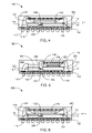
- FIG. 1 therein is shown a cross-sectional view of an integrated circuit packaging system 100 in a first embodiment of the present invention.
- the cross-sectional of the integrated circuit packaging system 100 depicts a package substrate 102 having a component side 104 and a system side 106 .
- System contacts 108 on the system side 106 may have system interconnects 110 , such as solder balls, solder bumps, solder columns, or stud bumps, provided for attaching to the next level system (not shown).
- a first integrated circuit die 112 such as a flip chip die, may be coupled to component contacts 114 , on the component side 104 of the package substrate 102 , by chip interconnects 116 .
- the chip interconnects 116 may include bond wires, solder balls, solder bumps, solder columns, or stud bumps.
- a sealant 118 such as an underfill material, may be injected around the chip interconnects 116 and between the component side 104 and the first integrated circuit die 112 .
- a second integrated circuit die 120 such as a flip chip die, may be coupled to the component contacts 114 , on the component side 104 of the package substrate 102 , by the chip interconnects 116 .
- the second integrated circuit die 120 may be positioned horizontally adjacent to and spaced from the first integrated circuit die 112 to form a gap 122 between the first integrated circuit die 112 and the second integrated circuit die 120 .
- the second integrated circuit die 120 can electrically connect to the package substrate 102 with a bond wire located on a side of the second integrated circuit die 120 facing away from the first integrated circuit die 112 .
- the sealant 118 may be injected around the chip interconnects 116 and between the component side 104 and the second integrated circuit die 120 .
- An internal package 124 such as a quad flatpack-no lead (QFN) or a ball grid array (BGA) package, may be mounted on the first integrated circuit die 112 and the second integrated circuit die 120 in an inverted position.
- An adhesive 126 may be applied between the internal package 124 , the first integrated circuit die 112 and the second integrated circuit die 120 .
- the internal package 124 may have one or more of an internal die 128 electrically connected to an internal package substrate 130 , providing internal package contacts 131 , and encapsulated by an internal package body 132 , such as formed from an epoxy molding compound.
- the internal package contacts 131 are on a side of the internal package 124 opposite of the first integrated circuit die 112 . Further, the internal package contacts 131 can be on the side of the internal package 124 exposed from the internal package body 132 . While the internal package 124 is shown with a single wire bond type of integrated circuit, this is an example only and other configurations are possible.
- the internal package substrate 130 may be electrically connected to the component side 104 of the package substrate 102 , by the chip interconnects 116 . This configuration allows a signal connection to be formed between the system interconnects 110 , the first integrated circuit die 112 , the second integrated circuit die 120 , the internal die 128 , or a combination thereof.
- a stacked package body 134 may be formed by molding the epoxy molding compound fully encapsulating the component side 104 of the package substrate 102 , the first integrated circuit die 112 , the second integrated circuit die 120 , the internal package 124 , the chip interconnects 116 , the sealant 118 , the adhesive 126 , and through the gap 122 . Further, the stacked package body 134 can fully encapsulate the internal package contacts 131 . The stacked package body 134 , while possibly formed of the same material as the internal package body 132 , remains identifiably different from the internal package body 132 because their boundary can be identified in cross-section.
- the configuration of the integrated circuit packaging system 100 may provide an extremely low profile package while supplying high functional density.
- This invention simplifies the design of the next level system by combining functions and reducing the number of interconnects required on the system printed circuit board (not shown).
- the integrated circuit packaging method and device of the present invention furnishes important and heretofore unknown and unavailable solutions, capabilities, and functional aspects for manufacturing high density and low profile package-in-package devices.
- FIG. 2 therein is shown a cross-sectional view of an integrated circuit packaging system 200 in a second embodiment of the present invention.
- the cross-sectional view of the integrated circuit packaging system 200 depicts the package substrate 102 having the first integrated circuit die 112 and the second integrated circuit die 120 mounted to the component side 104 and separated by the gap 122 .
- An internal package 202 may be mounted over the first integrated circuit die 112 and held in position by the adhesive 126 .
- the internal package 202 may have one or more of the internal die 128 electrically connected to the internal package substrate 130 and encapsulated by the internal package body 132 , such as formed from an epoxy molding compound. While the internal package 202 is shown with a single wire bond type of integrated circuit, this is an example only and other configurations are possible.
- the internal package 202 may be coupled to the component side 104 of the package substrate 102 by the chip interconnects 116 , such as bond wires. This configuration allows a signal connection to be formed between the system interconnects 110 , the first integrated circuit die 112 , the second integrated circuit die 120 , the internal die 128 , or the combination thereof.
- the stacked package body 134 may be formed by molding the epoxy molding compound on the component side 104 of the package substrate 102 , the first integrated circuit die 112 , the second integrated circuit die 120 , the internal package 202 , the chip interconnects 116 , the sealant 118 , the adhesive 126 , and through the gap 122 .
- the stacked package body 134 while possibly formed of the same material as the internal package body 132 , remains identifiably different from the internal package body 132 because their boundary can be identified in cross-section.
- FIG. 3 therein is shown a cross-sectional view of an integrated circuit packaging system 300 in a third embodiment of the present invention.
- the cross-sectional view of the integrated circuit packaging system 300 depicts the package substrate 102 having the first integrated circuit die 112 and the second integrated circuit die 120 mounted to the component side 104 and separated by the gap 122 .
- the internal package 202 may be mounted over the first integrated circuit die 112 and held in position by the adhesive 126 .
- a third integrated circuit die 302 such as a wire bond die, may be mounted over the second integrated circuit die 120 by the adhesive 126 .
- the chip interconnect 116 may couple the third integrated circuit die 302 to the component contacts 114 , on the component side 104 of the package substrate 102 .
- the internal package 202 may have one or more of the internal die 128 electrically connected to the internal package substrate 130 and encapsulated by the internal package body 132 , such as formed from an epoxy molding compound. While the internal package 124 is shown with a single wire bond type of integrated circuit, this is an example only and other configurations are possible.
- the internal package 202 may be coupled to the component side 104 of the package substrate 102 by the chip interconnect 116 , such as a bond wire. This configuration allows a signal connection to be formed between the system interconnects 110 , the first integrated circuit die 112 , the second integrated circuit die 120 , the third integrated circuit die 302 , the internal die 128 , or a combination thereof.
- the stacked package body 134 may be formed by molding the epoxy molding compound on the component side 104 of the package substrate 102 , the first integrated circuit die 112 , the second integrated circuit die 120 , the internal package 202 , the chip interconnects 116 , the sealant 118 , the adhesive 126 , and through the gap 122 .
- FIG. 4 therein is shown a cross-sectional view of an integrated circuit packaging system 400 in a fourth embodiment of the present invention.
- the cross-sectional view of the integrated circuit packaging system 400 depicts the package substrate 102 having the first integrated circuit die 112 , such as a wire bond die, and the second integrated circuit die 120 mounted to the component side 104 and separated by the gap 122 .
- the first integrated circuit die 112 may be coupled to the component contacts 114 by the chip interconnects 116 .
- the first integrated circuit die 112 may be mounted on the component side 104 by the adhesive 126 .
- the internal package 124 may be mounted over the first integrated circuit die 112 , held in position by a wire in film adhesive 402 on the first integrated circuit die 112 , and the second integrated circuit die 120 , held in position by the adhesive 126 .
- a gap contact 404 may be coupled to the first integrated circuit die 112 by the chip interconnect 116 .
- the chip interconnect 116 By coupling the first integrated circuit die 112 to the gap contact 404 an increased number of input/output interconnects is possible. This will further simplify the design of the system level substrate (not shown) by reducing the number of interconnect traces required in the system level substrate.
- the internal package 124 may have one or more of the internal die 128 electrically connected to the internal package substrate 130 and encapsulated by the internal package body 132 , such as formed from an epoxy molding compound. While the internal package 124 is shown with a single wire bond type of integrated circuit, this is an example only and other configurations are possible.
- the internal package 124 may be coupled to the component side 104 of the package substrate 102 by the chip interconnect 116 , such as a bond wire. This configuration allows a signal connection to be formed between the system interconnects 110 , the first integrated circuit die 112 , the second integrated circuit die 120 , the internal die 128 , or the combination thereof.
- the stacked package body 134 may be formed by molding the epoxy molding compound on the component side 104 of the package substrate 102 , the first integrated circuit die 112 , the second integrated circuit die 120 , the internal package 124 , the chip interconnects 116 , the sealant 118 , the adhesive 126 , the wire in film adhesive 402 , and through the gap 122 .
- the stacked package body 134 while possibly formed of the same material as the internal package body 132 , remains identifiably different from the internal package body 132 because their boundary can be identified in cross-section.
- FIG. 5 therein is shown a cross-sectional view of an integrated circuit packaging system 500 in a fifth embodiment of the present invention.
- the cross-sectional view of the integrated circuit packaging system 500 depicts the package substrate 102 having the first integrated circuit die 112 and the second integrated circuit die 120 , such as a wire bond die, mounted to the component side 104 and separated by the gap 122 .
- the internal package 202 may be mounted over the first integrated circuit die 112 and held in position by the adhesive 126 .
- the internal package 202 may have one or more of the internal die 128 electrically connected to the internal package substrate 130 and encapsulated by the internal package body 132 , such as formed from an epoxy molding compound. While the internal package 202 is shown with a single wire bond type of integrated circuit, this is an example only and other configurations are possible.
- the third integrated circuit die 302 such as a wire bond die, may be mounted over the second integrated circuit die 120 by the wire in film adhesive 402 .
- the third integrated circuit die 302 can be the same size as the second integrated circuit die 120 .
- the chip interconnects 116 may couple the third integrated circuit die 302 to the component contacts 114 , the internal package 202 , the gap contact 404 , or a combination thereof.
- the internal package 202 may be coupled to the component side 104 of the package substrate 102 by the chip interconnects 116 , such as bond wires. This configuration allows a signal connection to be formed between the system interconnects 110 , the first integrated circuit die 112 , the second integrated circuit die 120 , the third integrated circuit die 302 , the internal die 128 , or the combination thereof.
- the stacked package body 134 may be formed by molding the epoxy molding compound on the component side 104 of the package substrate 102 , the first integrated circuit die 112 , the second integrated circuit die 120 , the internal package 202 , the chip interconnects 116 , the sealant 118 , the wire in film adhesive 402 , the adhesive 126 , and through the gap 122 .
- the stacked package body 134 while possibly formed of the same material as the internal package body 132 , remains identifiably different from the internal package body 132 because their boundary can be identified in cross-section.
- FIG. 6 therein is shown a cross-sectional view of an integrated circuit packaging system 600 in a sixth embodiment of the present invention.
- the cross-sectional view of the integrated circuit packaging system 600 depicts the package substrate 102 having the first integrated circuit die 112 , such as a wire bond die, and the second integrated circuit die 120 mounted to the component side 104 and separated by the gap 122 .
- the first integrated circuit die 112 may be coupled to the component contacts 114 by the chip interconnects 116 .
- the gap contacts 404 in the gap 122 may be coupled to the first integrated circuit die 112 , the second integrated circuit die 120 , or a combination thereof.
- the first integrated circuit die 112 may be mounted on the component side 104 by the adhesive 126 .
- the internal package 124 may be mounted over the first integrated circuit die 112 and the second integrated circuit die 120 , held in position by the wire in film adhesive 402 .
- the internal package 124 may have one or more of the internal die 128 electrically connected to the internal package substrate 130 and encapsulated by the internal package body 132 , such as formed from an epoxy molding compound. While the internal package 124 is shown with a single wire bond type of integrated circuit, this is an example only and other configurations are possible.
- the internal package 124 may be coupled to the component side 104 of the package substrate 102 by the chip interconnect 116 , such as a bond wire. This configuration allows a signal connection to be formed between the system interconnects 110 , the first integrated circuit die 112 , the second integrated circuit die 120 , the internal die 128 , or the combination thereof.
- the stacked package body 134 may be formed by molding the epoxy molding compound on the component side 104 of the package substrate 102 , the first integrated circuit die 112 , the second integrated circuit die 120 , the internal package 124 , the chip interconnects 116 , the wire in film adhesive 402 , the adhesive 126 , and through the gap 122 .
- the stacked package body 134 while possibly formed of the same material as the internal package body 132 , remains identifiably different from the internal package body 132 because their boundary can be identified in cross-section.
- FIG. 7 therein is shown a cross-sectional view of an integrated circuit packaging system 700 in a seventh embodiment of the present invention.
- the cross-sectional view of the integrated circuit packaging system 700 depicts the package substrate 102 having the first integrated circuit die 112 and the second integrated circuit die 120 mounted to the component side 104 and separated by the gap 122 .
- the internal package 202 may be mounted over the first integrated circuit die 112 and held in position by the wire in film adhesive 402 .
- the internal package 202 may have one or more of the internal die 128 electrically connected to the internal package substrate 130 and encapsulated by the internal package body 132 , such as formed from an epoxy molding compound. While the internal package 202 is shown with a single wire bond type of integrated circuit, this is an example only and other configurations are possible.
- the internal package 202 may be coupled to the component contacts 114 , the second integrated circuit die 120 , the gap contacts 404 , or a combination thereof by the chip interconnects 116 , such as bond wires.
- the chip interconnects 116 are directly connected to the internal package 202 and the second integrated circuit die 120 .
- the chip interconnects 116 are also directly connected to the internal package 202 and the package substrate 102 . This configuration allows a signal connection to be formed between the system interconnects 110 , the first integrated circuit die 112 , the second integrated circuit die 120 , the internal die 128 , or the combination thereof.
- the stacked package body 134 may be formed by molding the epoxy molding compound on the component side 104 of the package substrate 102 , the first integrated circuit die 112 , the second integrated circuit die 120 , the internal package 202 , the chip interconnects 116 , the wire in film adhesive 402 , the adhesive 126 , and through the gap 122 .
- the stacked package body 134 while possibly formed of the same material as the internal package body 132 , remains identifiably different from the internal package body 132 because their boundary can be identified in cross-section.
- FIG. 8 therein is shown a cross-sectional view of an integrated circuit packaging system 800 in an eighth embodiment of the present invention.
- the cross-sectional view of the integrated circuit packaging system 800 depicts the package substrate 102 having the first integrated circuit die 112 and the second integrated circuit die 120 , such as wire bond die, mounted to the component side 104 , by the adhesive 126 , and separated by the gap 122 .
- the internal package 202 may be mounted over the first integrated circuit die 112 and held in position by the wire in film adhesive 402 .
- the internal package 202 may have one or more of the internal die 128 electrically connected to the internal package substrate 130 and encapsulated by the internal package body 132 , such as formed from an epoxy molding compound. While the internal package 202 is shown with a single wire bond type of integrated circuit, this is an example only and other configurations are possible.
- the third integrated circuit die 302 such as a wire bond die, may be mounted over the second integrated circuit die 120 by the wire in film adhesive 402 .
- the chip interconnects 116 may couple the third integrated circuit die 302 to the component contacts 114 , the internal package 202 , the gap contact 404 , or a combination thereof.
- the internal package 202 may be coupled to the component contacts 114 , the gap contacts 404 , the third integrated circuit die 302 , or a combination thereof by the chip interconnects 116 , such as bond wires.
- This configuration allows a signal connection to be formed between the system interconnects 110 , the first integrated circuit die 112 , the second integrated circuit die 120 , the third integrated circuit die 302 , the internal die 128 , or the combination thereof.
- the stacked package body 134 may be formed by molding the epoxy molding compound on the component side 104 of the package substrate 102 , the first integrated circuit die 112 , the second integrated circuit die 120 , the internal package 202 , the chip interconnects 116 , the wire in film adhesive 402 , the adhesive 126 , and through the gap 122 .
- the stacked package body 134 while possibly formed of the same material as the internal package body 132 , remains identifiably different from the internal package body 132 because their boundary can be identified in cross-section.
- FIG. 9 therein is shown a cross-sectional view of an integrated circuit packaging system 900 in a ninth embodiment of the present invention.
- the a cross-sectional view of the integrated circuit packaging system 900 depicts the package substrate 102 having the first integrated circuit die 112 and the second integrated circuit die 120 , such as wire bond die, mounted to the component side 104 , by the adhesive 126 , and separated by the gap 122 .
- the internal package 202 may be mounted over the first integrated circuit die 112 and held in position by the wire in film adhesive 402 .
- a fourth integrated circuit die 902 such as a flip chip die, may be mounted on the internal package contacts 131 of the internal package substrate 130 by the chip interconnects 116 , such as solder balls.
- the third integrated circuit die 302 such as a wire bond die, may be mounted over the second integrated circuit die 120 by the wire in film adhesive 402 .
- the chip interconnects 116 may couple the third integrated circuit die 302 to the component contacts 114 , the internal package 202 , the gap contact 404 , or a combination thereof.
- the internal package 202 may be coupled to the component contacts 114 , the gap contacts 404 , the third integrated circuit die 302 , or a combination thereof by the chip interconnects 116 , such as bond wires.
- This configuration allows a signal connection to be formed between the system interconnects 110 , the first integrated circuit die 112 , the second integrated circuit die 120 , the third integrated circuit die 302 , the fourth integrated circuit die 902 , the internal die 128 , or the combination thereof.
- the stacked package body 134 may be formed by molding the epoxy molding compound on the component side 104 of the package substrate 102 , the first integrated circuit die 112 , the second integrated circuit die 120 , the internal package 202 , the third integrated circuit die 302 , the fourth integrated circuit die 902 , the chip interconnects 116 , the sealant 118 , the adhesive 126 , and through the gap 122 .
- the stacked package body 134 while possibly formed of the same material as the internal package body 132 , remains identifiably different from the internal package body 132 because their boundary can be identified in cross-section.
- FIG. 10 therein is shown a bottom view of the integrated circuit packaging system 100 .
- the bottom view of the integrated circuit packaging system 100 depicts an array 1002 of the system interconnects 110 on the system side 106 .
- the section line 1 - 1 shows the position and direction of view for FIG. 1 . This is also substantially the same cross-section as shown in FIGS. 2-9 .
- the method 1100 includes: providing a package substrate, having a component side and a system side in a block 1102 ; mounting a first integrated circuit die on the component side of the package substrate in a block 1104 ; mounting a second integrated circuit die on the component side of the package substrate in a block 1106 ; mounting an internal package, having an internal die, over the first integrated circuit die; coupling chip interconnects between the first integrated circuit die, the second integrated circuit die, the internal die, the component side, or a combination thereof in a block 1108 ; and forming a stacked package body by encapsulating the component side, the first integrated circuit die, the second integrated circuit die, the internal package, and the chip interconnects in a block 1110 .
- the resulting method, process, apparatus, device, product, and/or system is straightforward, cost-effective, uncomplicated, highly versatile and effective, can be surprisingly and unobviously implemented by adapting known technologies, and are thus readily suited for efficiently and economically manufacturing package-in-package systems fully compatible with conventional manufacturing methods or processes and technologies.
- Another important aspect of the present invention is that it valuably supports and services the historical trend of reducing costs, simplifying systems, and increasing performance.
Abstract
Description
Claims (16)
Priority Applications (2)
| Application Number | Priority Date | Filing Date | Title |
|---|---|---|---|
| US12/404,279 US8816487B2 (en) | 2008-03-18 | 2009-03-13 | Integrated circuit packaging system with package-in-package and method of manufacture thereof |
| TW099106558A TWI541910B (en) | 2009-03-13 | 2010-03-08 | Integrated circuit packaging system with package-in-package and method of manufacture thereof |
Applications Claiming Priority (2)
| Application Number | Priority Date | Filing Date | Title |
|---|---|---|---|
| US3770208P | 2008-03-18 | 2008-03-18 | |
| US12/404,279 US8816487B2 (en) | 2008-03-18 | 2009-03-13 | Integrated circuit packaging system with package-in-package and method of manufacture thereof |
Publications (2)
| Publication Number | Publication Date |
|---|---|
| US20090236723A1 US20090236723A1 (en) | 2009-09-24 |
| US8816487B2 true US8816487B2 (en) | 2014-08-26 |
Family
ID=41088042
Family Applications (1)
| Application Number | Title | Priority Date | Filing Date |
|---|---|---|---|
| US12/404,279 Active 2029-08-27 US8816487B2 (en) | 2008-03-18 | 2009-03-13 | Integrated circuit packaging system with package-in-package and method of manufacture thereof |
Country Status (1)
| Country | Link |
|---|---|
| US (1) | US8816487B2 (en) |
Cited By (1)
| Publication number | Priority date | Publication date | Assignee | Title |
|---|---|---|---|---|
| US11309300B2 (en) | 2017-11-13 | 2022-04-19 | Samsung Electronics Co., Ltd. | Semiconductor package including processor chip and memory chip |
Families Citing this family (6)
| Publication number | Priority date | Publication date | Assignee | Title |
|---|---|---|---|---|
| US7923290B2 (en) * | 2009-03-27 | 2011-04-12 | Stats Chippac Ltd. | Integrated circuit packaging system having dual sided connection and method of manufacture thereof |
| US8409917B2 (en) * | 2011-03-22 | 2013-04-02 | Stats Chippac Ltd. | Integrated circuit packaging system with an interposer substrate and method of manufacture thereof |
| TWI548042B (en) * | 2013-04-23 | 2016-09-01 | 巨擘科技股份有限公司 | Electrical system and core module thereof |
| CN104538368A (en) * | 2014-12-30 | 2015-04-22 | 华天科技(西安)有限公司 | Three-dimensional stacking packaging structure based on secondary plastic packaging technology and preparing method thereof |
| WO2019066988A1 (en) * | 2017-09-30 | 2019-04-04 | Intel Corporation | Pcb/package embedded stack for double sided interconnect |
| CN114300446B (en) * | 2022-03-09 | 2022-07-08 | 甬矽电子(宁波)股份有限公司 | Chip stacking shielding structure and manufacturing method thereof |
Citations (14)
| Publication number | Priority date | Publication date | Assignee | Title |
|---|---|---|---|---|
| US6906416B2 (en) | 2002-10-08 | 2005-06-14 | Chippac, Inc. | Semiconductor multi-package module having inverted second package stacked over die-up flip-chip ball grid array (BGA) package |
| US6951774B2 (en) | 2001-04-06 | 2005-10-04 | Renesas Technology Corp. | Semiconductor device and method of manufacturing the same |
| US20060131719A1 (en) * | 2003-05-30 | 2006-06-22 | Seiko Epson Corporation | Semiconductor device, electronic device, electronic apparatus, and method of manufacturing semiconductor device |
| US20060186524A1 (en) * | 2005-02-18 | 2006-08-24 | Fujitsu Limited | Semiconductor device |
| US20070052082A1 (en) | 2005-09-02 | 2007-03-08 | Cheng-Yin Lee | Multi-chip package structure |
| US20070194423A1 (en) * | 2006-02-17 | 2007-08-23 | Stats Chippac Ltd. | Stacked integrated circuit package-in-package system with recessed spacer |
| US20070257377A1 (en) * | 2006-05-04 | 2007-11-08 | Da-Jung Chen | Package structure |
| US20080157331A1 (en) * | 2006-12-27 | 2008-07-03 | Masanori Onodera | Semiconductor device and method of manufacturing the same |
| US20080197470A1 (en) * | 2004-05-20 | 2008-08-21 | Kabushiki Kaisha Toshiba | Stacked electronic component and manufacturing method thereof |
| US20080203566A1 (en) * | 2007-02-27 | 2008-08-28 | Chao-Yuan Su | Stress buffer layer for packaging process |
| US20090051019A1 (en) * | 2007-08-20 | 2009-02-26 | Chih-Feng Huang | Multi-chip module package |
| US20090152701A1 (en) * | 2007-12-18 | 2009-06-18 | Heap Hoe Kuan | Integrated circuit package system with package integration |
| US20090212442A1 (en) * | 2008-02-22 | 2009-08-27 | Seng Guan Chow | Integrated circuit package system with penetrable film adhesive |
| US20090224390A1 (en) * | 2008-03-10 | 2009-09-10 | Yang Deokkyung | Integrated circuit with step molded inner stacking module package in package system |
-
2009
- 2009-03-13 US US12/404,279 patent/US8816487B2/en active Active
Patent Citations (16)
| Publication number | Priority date | Publication date | Assignee | Title |
|---|---|---|---|---|
| US6951774B2 (en) | 2001-04-06 | 2005-10-04 | Renesas Technology Corp. | Semiconductor device and method of manufacturing the same |
| US6933598B2 (en) | 2002-10-08 | 2005-08-23 | Chippac, Inc. | Semiconductor stacked multi-package module having inverted second package and electrically shielded first package |
| US7101731B2 (en) | 2002-10-08 | 2006-09-05 | Chippac, Inc. | Semiconductor multi-package module having inverted second package stacked over die-up flip-chip ball grid array (BGA) package |
| US6906416B2 (en) | 2002-10-08 | 2005-06-14 | Chippac, Inc. | Semiconductor multi-package module having inverted second package stacked over die-up flip-chip ball grid array (BGA) package |
| US20060131719A1 (en) * | 2003-05-30 | 2006-06-22 | Seiko Epson Corporation | Semiconductor device, electronic device, electronic apparatus, and method of manufacturing semiconductor device |
| US20080197470A1 (en) * | 2004-05-20 | 2008-08-21 | Kabushiki Kaisha Toshiba | Stacked electronic component and manufacturing method thereof |
| US20060186524A1 (en) * | 2005-02-18 | 2006-08-24 | Fujitsu Limited | Semiconductor device |
| US20070052082A1 (en) | 2005-09-02 | 2007-03-08 | Cheng-Yin Lee | Multi-chip package structure |
| US20070194423A1 (en) * | 2006-02-17 | 2007-08-23 | Stats Chippac Ltd. | Stacked integrated circuit package-in-package system with recessed spacer |
| US20070257377A1 (en) * | 2006-05-04 | 2007-11-08 | Da-Jung Chen | Package structure |
| US20080157331A1 (en) * | 2006-12-27 | 2008-07-03 | Masanori Onodera | Semiconductor device and method of manufacturing the same |
| US20080203566A1 (en) * | 2007-02-27 | 2008-08-28 | Chao-Yuan Su | Stress buffer layer for packaging process |
| US20090051019A1 (en) * | 2007-08-20 | 2009-02-26 | Chih-Feng Huang | Multi-chip module package |
| US20090152701A1 (en) * | 2007-12-18 | 2009-06-18 | Heap Hoe Kuan | Integrated circuit package system with package integration |
| US20090212442A1 (en) * | 2008-02-22 | 2009-08-27 | Seng Guan Chow | Integrated circuit package system with penetrable film adhesive |
| US20090224390A1 (en) * | 2008-03-10 | 2009-09-10 | Yang Deokkyung | Integrated circuit with step molded inner stacking module package in package system |
Cited By (1)
| Publication number | Priority date | Publication date | Assignee | Title |
|---|---|---|---|---|
| US11309300B2 (en) | 2017-11-13 | 2022-04-19 | Samsung Electronics Co., Ltd. | Semiconductor package including processor chip and memory chip |
Also Published As
| Publication number | Publication date |
|---|---|
| US20090236723A1 (en) | 2009-09-24 |
Similar Documents
| Publication | Publication Date | Title |
|---|---|---|
| US7919871B2 (en) | Integrated circuit package system for stackable devices | |
| US7518226B2 (en) | Integrated circuit packaging system with interposer | |
| US8541872B2 (en) | Integrated circuit package system with package stacking and method of manufacture thereof | |
| US7847382B2 (en) | Integrated circuit packaging system with package stacking and method of manufacture thereof | |
| US9236319B2 (en) | Stacked integrated circuit package system | |
| US8592973B2 (en) | Integrated circuit packaging system with package-on-package stacking and method of manufacture thereof | |
| US7859120B2 (en) | Package system incorporating a flip-chip assembly | |
| US8188586B2 (en) | Mountable integrated circuit package system with mounting interconnects | |
| US8466567B2 (en) | Integrated circuit packaging system with stack interconnect and method of manufacture thereof | |
| US8559185B2 (en) | Integrated circuit package system with stackable devices and a method of manufacture thereof | |
| US9093391B2 (en) | Integrated circuit packaging system with fan-in package and method of manufacture thereof | |
| US8106499B2 (en) | Integrated circuit packaging system with a dual substrate package and method of manufacture thereof | |
| US8749040B2 (en) | Integrated circuit packaging system with package-on-package and method of manufacture thereof | |
| US7927917B2 (en) | Integrated circuit packaging system with inward and outward interconnects and method of manufacture thereof | |
| US8723309B2 (en) | Integrated circuit packaging system with through silicon via and method of manufacture thereof | |
| US8698294B2 (en) | Integrated circuit package system including wide flange leadframe | |
| US8816487B2 (en) | Integrated circuit packaging system with package-in-package and method of manufacture thereof | |
| US9530753B2 (en) | Integrated circuit packaging system with chip stacking and method of manufacture thereof | |
| US20120319294A1 (en) | Integrated circuit packaging system with laser hole and method of manufacture thereof | |
| US20110256664A1 (en) | Integrated circuit packaging system with mountable inward and outward interconnects and method of manufacture thereof | |
| US8368199B2 (en) | Integrated circuit package system for stackable devices and method for manufacturing thereof | |
| US8981577B2 (en) | Integrated circuit packaging system with interconnect and method of manufacture thereof | |
| US7919848B2 (en) | Integrated circuit package system with multiple devices | |
| TWI541910B (en) | Integrated circuit packaging system with package-in-package and method of manufacture thereof |
Legal Events
| Date | Code | Title | Description |
|---|---|---|---|
| AS | Assignment |
Owner name: STATS CHIPPAC LTD., SINGAPORE Free format text: ASSIGNMENT OF ASSIGNORS INTEREST;ASSIGNORS:BAE, HYUNIL;KIM, YOUNGCHUL;LEE, MYUNG KIL;REEL/FRAME:022430/0762 Effective date: 20090312 |
|
| STCF | Information on status: patent grant |
Free format text: PATENTED CASE |
|
| AS | Assignment |
Owner name: CITICORP INTERNATIONAL LIMITED, AS COMMON SECURITY AGENT, HONG KONG Free format text: SECURITY INTEREST;ASSIGNORS:STATS CHIPPAC, INC.;STATS CHIPPAC LTD.;REEL/FRAME:036288/0748 Effective date: 20150806 Owner name: CITICORP INTERNATIONAL LIMITED, AS COMMON SECURITY Free format text: SECURITY INTEREST;ASSIGNORS:STATS CHIPPAC, INC.;STATS CHIPPAC LTD.;REEL/FRAME:036288/0748 Effective date: 20150806 |
|
| AS | Assignment |
Owner name: STATS CHIPPAC PTE. LTE., SINGAPORE Free format text: CHANGE OF NAME;ASSIGNOR:STATS CHIPPAC LTD.;REEL/FRAME:038378/0208 Effective date: 20160329 |
|
| MAFP | Maintenance fee payment |
Free format text: PAYMENT OF MAINTENANCE FEE, 4TH YEAR, LARGE ENTITY (ORIGINAL EVENT CODE: M1551) Year of fee payment: 4 |
|
| AS | Assignment |
Owner name: STATS CHIPPAC PTE. LTD. FORMERLY KNOWN AS STATS CHIPPAC LTD., SINGAPORE Free format text: RELEASE BY SECURED PARTY;ASSIGNOR:CITICORP INTERNATIONAL LIMITED, AS COMMON SECURITY AGENT;REEL/FRAME:052844/0491 Effective date: 20190503 Owner name: STATS CHIPPAC, INC., CALIFORNIA Free format text: RELEASE BY SECURED PARTY;ASSIGNOR:CITICORP INTERNATIONAL LIMITED, AS COMMON SECURITY AGENT;REEL/FRAME:052844/0491 Effective date: 20190503 |
|
| MAFP | Maintenance fee payment |
Free format text: PAYMENT OF MAINTENANCE FEE, 8TH YEAR, LARGE ENTITY (ORIGINAL EVENT CODE: M1552); ENTITY STATUS OF PATENT OWNER: LARGE ENTITY Year of fee payment: 8 |
|
| AS | Assignment |
Owner name: STATS CHIPPAC PTE. LTD., SINGAPORE Free format text: CORRECTIVE ASSIGNMENT TO CORRECT THE CORRECT THE SPELLING OF ASSIGNEE'S NAME FROM "STATS CHIPPAC PTE. LTE." TO "STATS CHIPPAC PTE. LTD." PREVIOUSLY RECORDED AT REEL: 038378 FRAME: 0208. ASSIGNOR(S) HEREBY CONFIRMS THE ASSIGNMENT;ASSIGNOR:STATS CHIPPAC LTD.;REEL/FRAME:064803/0387 Effective date: 20160329 |