US8846195B2 - Ultra-thin polymeric adhesion layer - Google Patents
Ultra-thin polymeric adhesion layer Download PDFInfo
- Publication number
- US8846195B2 US8846195B2 US12/326,709 US32670908A US8846195B2 US 8846195 B2 US8846195 B2 US 8846195B2 US 32670908 A US32670908 A US 32670908A US 8846195 B2 US8846195 B2 US 8846195B2
- Authority
- US
- United States
- Prior art keywords
- polymeric
- adhesion layer
- substrate
- composition
- imprint
- Prior art date
- Legal status (The legal status is an assumption and is not a legal conclusion. Google has not performed a legal analysis and makes no representation as to the accuracy of the status listed.)
- Active, expires
Links
Images


Classifications
-
- G—PHYSICS
- G03—PHOTOGRAPHY; CINEMATOGRAPHY; ANALOGOUS TECHNIQUES USING WAVES OTHER THAN OPTICAL WAVES; ELECTROGRAPHY; HOLOGRAPHY
- G03F—PHOTOMECHANICAL PRODUCTION OF TEXTURED OR PATTERNED SURFACES, e.g. FOR PRINTING, FOR PROCESSING OF SEMICONDUCTOR DEVICES; MATERIALS THEREFOR; ORIGINALS THEREFOR; APPARATUS SPECIALLY ADAPTED THEREFOR
- G03F7/00—Photomechanical, e.g. photolithographic, production of textured or patterned surfaces, e.g. printing surfaces; Materials therefor, e.g. comprising photoresists; Apparatus specially adapted therefor
- G03F7/004—Photosensitive materials
- G03F7/038—Macromolecular compounds which are rendered insoluble or differentially wettable
- G03F7/0388—Macromolecular compounds which are rendered insoluble or differentially wettable with ethylenic or acetylenic bands in the side chains of the photopolymer
-
- G—PHYSICS
- G03—PHOTOGRAPHY; CINEMATOGRAPHY; ANALOGOUS TECHNIQUES USING WAVES OTHER THAN OPTICAL WAVES; ELECTROGRAPHY; HOLOGRAPHY
- G03F—PHOTOMECHANICAL PRODUCTION OF TEXTURED OR PATTERNED SURFACES, e.g. FOR PRINTING, FOR PROCESSING OF SEMICONDUCTOR DEVICES; MATERIALS THEREFOR; ORIGINALS THEREFOR; APPARATUS SPECIALLY ADAPTED THEREFOR
- G03F7/00—Photomechanical, e.g. photolithographic, production of textured or patterned surfaces, e.g. printing surfaces; Materials therefor, e.g. comprising photoresists; Apparatus specially adapted therefor
- G03F7/0002—Lithographic processes using patterning methods other than those involving the exposure to radiation, e.g. by stamping
-
- B—PERFORMING OPERATIONS; TRANSPORTING
- B32—LAYERED PRODUCTS
- B32B—LAYERED PRODUCTS, i.e. PRODUCTS BUILT-UP OF STRATA OF FLAT OR NON-FLAT, e.g. CELLULAR OR HONEYCOMB, FORM
- B32B7/00—Layered products characterised by the relation between layers; Layered products characterised by the relative orientation of features between layers, or by the relative values of a measurable parameter between layers, i.e. products comprising layers having different physical, chemical or physicochemical properties; Layered products characterised by the interconnection of layers
- B32B7/02—Physical, chemical or physicochemical properties
-
- B—PERFORMING OPERATIONS; TRANSPORTING
- B82—NANOTECHNOLOGY
- B82Y—SPECIFIC USES OR APPLICATIONS OF NANOSTRUCTURES; MEASUREMENT OR ANALYSIS OF NANOSTRUCTURES; MANUFACTURE OR TREATMENT OF NANOSTRUCTURES
- B82Y10/00—Nanotechnology for information processing, storage or transmission, e.g. quantum computing or single electron logic
-
- B—PERFORMING OPERATIONS; TRANSPORTING
- B82—NANOTECHNOLOGY
- B82Y—SPECIFIC USES OR APPLICATIONS OF NANOSTRUCTURES; MEASUREMENT OR ANALYSIS OF NANOSTRUCTURES; MANUFACTURE OR TREATMENT OF NANOSTRUCTURES
- B82Y30/00—Nanotechnology for materials or surface science, e.g. nanocomposites
-
- B—PERFORMING OPERATIONS; TRANSPORTING
- B82—NANOTECHNOLOGY
- B82Y—SPECIFIC USES OR APPLICATIONS OF NANOSTRUCTURES; MEASUREMENT OR ANALYSIS OF NANOSTRUCTURES; MANUFACTURE OR TREATMENT OF NANOSTRUCTURES
- B82Y40/00—Manufacture or treatment of nanostructures
-
- Y—GENERAL TAGGING OF NEW TECHNOLOGICAL DEVELOPMENTS; GENERAL TAGGING OF CROSS-SECTIONAL TECHNOLOGIES SPANNING OVER SEVERAL SECTIONS OF THE IPC; TECHNICAL SUBJECTS COVERED BY FORMER USPC CROSS-REFERENCE ART COLLECTIONS [XRACs] AND DIGESTS
- Y10—TECHNICAL SUBJECTS COVERED BY FORMER USPC
- Y10T—TECHNICAL SUBJECTS COVERED BY FORMER US CLASSIFICATION
- Y10T428/00—Stock material or miscellaneous articles
- Y10T428/26—Web or sheet containing structurally defined element or component, the element or component having a specified physical dimension
- Y10T428/261—In terms of molecular thickness or light wave length
-
- Y—GENERAL TAGGING OF NEW TECHNOLOGICAL DEVELOPMENTS; GENERAL TAGGING OF CROSS-SECTIONAL TECHNOLOGIES SPANNING OVER SEVERAL SECTIONS OF THE IPC; TECHNICAL SUBJECTS COVERED BY FORMER USPC CROSS-REFERENCE ART COLLECTIONS [XRACs] AND DIGESTS
- Y10—TECHNICAL SUBJECTS COVERED BY FORMER USPC
- Y10T—TECHNICAL SUBJECTS COVERED BY FORMER US CLASSIFICATION
- Y10T428/00—Stock material or miscellaneous articles
- Y10T428/26—Web or sheet containing structurally defined element or component, the element or component having a specified physical dimension
- Y10T428/263—Coating layer not in excess of 5 mils thick or equivalent
- Y10T428/264—Up to 3 mils
- Y10T428/265—1 mil or less
-
- Y—GENERAL TAGGING OF NEW TECHNOLOGICAL DEVELOPMENTS; GENERAL TAGGING OF CROSS-SECTIONAL TECHNOLOGIES SPANNING OVER SEVERAL SECTIONS OF THE IPC; TECHNICAL SUBJECTS COVERED BY FORMER USPC CROSS-REFERENCE ART COLLECTIONS [XRACs] AND DIGESTS
- Y10—TECHNICAL SUBJECTS COVERED BY FORMER USPC
- Y10T—TECHNICAL SUBJECTS COVERED BY FORMER US CLASSIFICATION
- Y10T428/00—Stock material or miscellaneous articles
- Y10T428/26—Web or sheet containing structurally defined element or component, the element or component having a specified physical dimension
- Y10T428/269—Web or sheet containing structurally defined element or component, the element or component having a specified physical dimension including synthetic resin or polymer layer or component
-
- Y—GENERAL TAGGING OF NEW TECHNOLOGICAL DEVELOPMENTS; GENERAL TAGGING OF CROSS-SECTIONAL TECHNOLOGIES SPANNING OVER SEVERAL SECTIONS OF THE IPC; TECHNICAL SUBJECTS COVERED BY FORMER USPC CROSS-REFERENCE ART COLLECTIONS [XRACs] AND DIGESTS
- Y10—TECHNICAL SUBJECTS COVERED BY FORMER USPC
- Y10T—TECHNICAL SUBJECTS COVERED BY FORMER US CLASSIFICATION
- Y10T428/00—Stock material or miscellaneous articles
- Y10T428/28—Web or sheet containing structurally defined element or component and having an adhesive outermost layer
- Y10T428/2848—Three or more layers
-
- Y—GENERAL TAGGING OF NEW TECHNOLOGICAL DEVELOPMENTS; GENERAL TAGGING OF CROSS-SECTIONAL TECHNOLOGIES SPANNING OVER SEVERAL SECTIONS OF THE IPC; TECHNICAL SUBJECTS COVERED BY FORMER USPC CROSS-REFERENCE ART COLLECTIONS [XRACs] AND DIGESTS
- Y10—TECHNICAL SUBJECTS COVERED BY FORMER USPC
- Y10T—TECHNICAL SUBJECTS COVERED BY FORMER US CLASSIFICATION
- Y10T428/00—Stock material or miscellaneous articles
- Y10T428/28—Web or sheet containing structurally defined element or component and having an adhesive outermost layer
- Y10T428/2852—Adhesive compositions
- Y10T428/287—Adhesive compositions including epoxy group or epoxy polymer
Definitions
- the field of invention relates generally to nano-fabrication of structures. More particularly, the present invention is directed to an ultra-thin polymeric adhesion layer.
- Nano-fabrication includes the fabrication of very small structures that have features on the order of 100 nanometers or smaller.
- One application in which nano-fabrication has had a sizeable impact is in the processing of integrated circuits.
- the semiconductor processing industry continues to strive for larger production yields while increasing the circuits per unit area formed on a substrate, therefore nano-fabrication becomes increasingly important.
- Nano-fabrication provides greater process control while allowing continued reduction of the minimum feature dimensions of the structures formed.
- Other areas of development in which nano-fabrication has been employed include biotechnology, optical technology, mechanical systems, and the like.
- imprint lithography An exemplary nano-fabrication technique in use today is commonly referred to as imprint lithography.
- Exemplary imprint lithography processes are described in detail in numerous publications, such as U.S. Patent Application Publication No. 2004/0065976, U.S. Patent Application Publication No. 2004/0065252, and U.S. Pat. No. 6,936,194, all of which are hereby incorporated by reference herein.
- An imprint lithography technique disclosed in each of the aforementioned U.S. patent application publications and patent includes formation of a relief pattern in a formable (polymerizable) layer and transferring a pattern corresponding to the relief pattern into an underlying substrate.
- the substrate may be coupled to a motion stage to obtain a desired positioning to facilitate the patterning process.
- the patterning process uses a template spaced apart from the substrate and the formable liquid applied between the template and the substrate.
- the formable liquid is solidified to form a rigid layer that has a pattern conforming to a shape of the surface of the template that contacts the formable liquid.
- the template is separated from the rigid layer such that the template and the substrate are spaced apart.
- the substrate and the solidified layer are then subjected to additional processes to transfer a relief image into the substrate that corresponds to the pattern in the solidified layer.
- an imprint lithography imprinting stack includes a substrate and a polymeric adhesion layer adhered to the substrate.
- an adhesion layer is formed on an imprint lithography substrate by spin-coating a polymerizable composition onto an imprint lithography substrate, and solidifying the polymerizable composition to form a polymeric adhesion layer adhered to the imprint lithography substrate.
- a polymerizable composition is spin-coated on an imprint lithography substrate.
- the polymerizable composition includes polymeric components with an extended backbone length of at least about 2 nm. The backbones of the polymeric components are substantially aligned in a planar configuration along a surface of the imprint lithography substrate.
- the polymerizable composition is solidified to form a polymeric adhesion layer.
- a thickness of the polymeric adhesion layer is less than about 2 nm.
- a thickness of the polymeric adhesion layer is about 1 nm.
- the polymeric adhesion layer may be formed from a composition including a polymeric component with an extended backbone length of at least about 2 nm.
- the polymeric component is synthesized from a compound including an aromatic group.
- the polymeric component is synthesized from a cresol epoxy novolac.
- the polymeric component includes a carboxylic functional group capable of bonding to the substrate and an additional functional group capable of bonding with an imprint resist.
- the polymeric adhesion layer may be capable of bonding with an imprint resist during solidification of the imprint resist on the imprinting stack.
- FIG. 1 is a simplified plan view of a lithographic system in accordance with the prior art
- FIG. 2 is a simplified elevation view of a template and imprinting material disposed on a substrate in accordance with the present invention
- FIG. 3 is a simplified elevation view of the template and substrate, shown in FIG. 2 , with the imprinting material being shown as patterned and solidified upon the layer;
- FIG. 4 is a cross-sectional view of the template contacting imprinting material demonstrating the formation of the weak boundary lamella between solidified imprinting material and a template;
- FIG. 5 is a detailed view of the droplets of imprint material, shown in FIG. 2 , showing the bifurcation of the droplets into surfactant-rich regions and surfactant-depleted regions;
- FIG. 6 is a detailed view of a layer of imprinting material, deposited employing spin-on techniques, showing the bifurcation of the layer into surfactant-rich regions and surfactant-depleted regions;
- FIG. 7 is a cross-sectional view of the template contacting solidified imprinting material, deposited as shown in either FIG. 5 or 6 , formed on a substrate including a primer layer;
- FIG. 8 illustrates a chemical structure of a component of a composition that may be employed to form a primer layer
- FIG. 9 illustrates a chemical structure of a component of a composition that may be employed to form a primer layer
- FIG. 10 illustrates a chemical structure of a component of a composition that may be employed to form the primer layer
- FIG. 11 illustrates a chemical structure of a component of a composition that may be employed to form a primer layer
- FIGS. 12A and 12B illustrate measurement locations for thickness measurement of a polymeric adhesion layer
- FIG. 13 is a scanning electron micrograph image of a cross-section of silicon wafer coated with a polymeric adhesion layer.
- a mold 36 in accordance with the present invention, may be employed in system 10 , and may define a surface having a substantially smooth or planar profile (not shown).
- mold 36 may include features defined by a plurality of spaced-apart recessions 38 and protrusions 40 .
- the plurality of features defines an original pattern that forms the basis of a pattern to be formed on a substrate 42 .
- Substrate 42 may comprise a bare wafer or a wafer with one or more layers disposed thereon, one of which is shown as primer layer 45 . To that end, reduced is a distance “d” between mold 36 and substrate 42 .
- the features on mold 36 may be imprinted into a conformable region of substrate 42 , such as an imprinting material disposed on a portion of surface 44 that presents a substantially planar profile.
- the imprinting material may be deposited using any known technique, e.g., spin-coating, dip coating and the like. In the present example, however, the imprinting material is deposited as a plurality of spaced-apart discrete droplets 46 on substrate 42 .
- Imprinting material is formed from a composition that may be selectively polymerized and cross-linked to record the original pattern therein, defining a recorded pattern.
- the pattern recorded in the imprinting material is produced, in part, by interaction with mold 36 , e.g., electrical interaction, magnetic interaction, thermal interaction, mechanical interaction or the like.
- mold 36 comes into mechanical contact with the imprinting material, spreading droplets 36 , so as to generate a contiguous formation 50 of the imprinting material over surface 44 .
- distance “d” is reduced to allow sub-portions 52 of imprinting material to ingress into and fill recessions 38 .
- the atmosphere between mold 36 and droplets 46 is saturated with helium or is completely evacuated or is a partially evacuated atmosphere of helium.
- the imprinting material may fill recessions 38 while covering surface 44 with a contiguous formation of the imprinting material.
- sub-portions 54 of imprinting material in superimposition with protrusions 40 remain after the desired, usually minimum, distance “d” has been reached.
- This action provides formation 50 with sub-portions 52 having a thickness t 1 , and sub-portions 54 , having a thickness t 2 .
- Thicknesses “t 1 ” and “t 2 ” may be any thickness desired, dependent upon the application.
- formation 50 is solidified by exposing the same to the appropriate curing agent, e.g., actinic energy, such as broadband ultra violet energy, thermal energy or the like, depending upon the imprinting material.
- formation 50 is solidified to provide side 56 thereof with a shape conforming to a shape of a surface 58 of mold 36 .
- the characteristics of the imprinting material are important to efficiently pattern substrate 42 in light of the unique patterning process employed.
- the imprinting material it is desired that the imprinting material have certain characteristics to facilitate rapid and even filling of the features of mold 36 so that all thicknesses t 1 are substantially uniform and all thicknesses t 2 are substantially uniform.
- the viscosity of the imprinting material it is desirable that the viscosity of the imprinting material be established, based upon the deposition process employed, to achieve the aforementioned characteristics.
- the imprinting material may be deposited on substrate 42 employing various techniques.
- a composition from which the imprinting material is formed have relatively low viscosity, e.g., in a range of 0.5 to 20 centipoises (cP).
- cP centipoises
- the composition provides the imprinting material with certain solidified phase characteristics.
- substrate 42 may be formed from silicon, plastics, gallium arsenide, mercury telluride, and composites thereof.
- substrate 42 may include one or more layers shown as primer layer 45 , e.g., dielectric layer, metal layer, semiconductor layer, planarization layer and the like, upon which formation 50 is generated.
- primer layer 45 would be deposited upon a wafer 47 employing any suitable technique, such as chemical vapor deposition, spin-coating and the like.
- primer layer 45 may be formed from any suitable material, such as silicon, germanium and the like.
- mold 36 may be formed from several materials, e.g., fused-silica, quartz, indium tin oxide diamond-like carbon, MoSi, sol-gels and the like.
- composition from which formation 50 is generated may be fabricated from several different families of bulk materials.
- the composition may be fabricated from vinyl ethers, methacrylates, epoxies, thiol-enes and acrylates, just to name a few.
- An exemplary bulk material from which to form formation 50 is as follows:
- the acrylate component isobornyl acrylate (IBOA)
- IBOA isobornyl acrylate
- IBOA is Sartomer Company, Inc. of Exton, Pa. available under the product name SR 506.
- n-hexyl acrylate (n-HA) has the following structure:
- n-HA is employed to reduce the viscosity of the bulk material so that bulk material, in the liquid phase, has a viscosity less than about 10 cP.
- An exemplary source for the n-HA component is the Aldrich Chemical Company of Milwaukee, Wis.
- a cross-linking component ethylene glycol diacrylate, has the following structure:
- EGDA also contributes to the modulus and stiffness buildup, as well as facilitates cross-linking of n-HA and IBOA during polymerization of the bulk material.
- An initiator component 2-hydroxy-2-methyl-1-phenyl-propan-1-one is available from Ciba Specialty Chemicals of Tarrytown, N.Y. under the trade name DAROCUR® 1173, and has the following structure:
- the actinic energy to which the initiator is responsive is broad band ultra-violet energy generated by a medium-pressure mercury lamp. In this manner, the initiator facilitates cross-linking and polymerization of the components of the bulk material.
- the surfactant component rises, after a period of time, to the air liquid interface, providing droplets 146 of imprinting material with a bifurcated concentration of materials.
- droplets 146 include a higher concentration of the surfactant component, referred to as a surfactant-component-rich (SCR) sub-portion 136 , than the second portion, referred to as a surfactant-component-depleted (SCD) sub-portion 137 .
- SCR sub-rich sub-portion 136 a surfactant-component-rich
- SCD sub-portion 137 is positioned between surface 44 and SCR sub-portion 136 .
- SCR sub-portion 136 attenuates the adhesion forces between mold 36 and the imprinting material, once the imprinting material is solidified.
- the surfactant component has opposed ends.
- the imprinting material is in the liquid phase, i.e., polymerizable, one of the opposed ends has an affinity for the bulk material included in the imprinting material.
- the remaining end has a fluorine component.
- the surfactant component is orientated so that the fluorine component extends from an air-liquid interface defined by the imprinting material and the surrounding ambient.
- Lamella 60 Upon solidification of the imprinting material, a first portion of the imprinting material generates a lamella 60 and a second portion of the imprinting material is solidified, i.e., polymeric material shown as formation 50 .
- Lamella 60 is positioned between formation 50 and mold 36 .
- Lamella 60 results from the presence and location of the fluorine components in the SCR sub-portion 136 .
- Lamella 60 prevents strong adhesion forces from being developed between mold 36 and formation 50 .
- formation 50 has first and second opposed sides 62 and 64 .
- Side 62 adheres to mold 36 with a first adhesion force.
- Side 64 adheres to substrate 42 with a second adhesion force.
- Lamella 60 results in the first adhesion force being less than the second adhesion force.
- mold 36 may be easily removed from formation 50 while minimizing distortions and/or the force required to separate mold 36 therefrom.
- formation 50 is shown with side 62 being patterned, it should be understood that side
- lamella 60 so as to be disposed between formation 50 and substrate 42 .
- This may be achieved, for example, by applying imprinting material to mold 36 and subsequently contacting substrate 42 with the imprinting material on mold 36 .
- formation 50 will be disposed between lamella 60 and the body, e.g., mold 36 or substrate 42 , upon which the polymerizable material is deposited.
- the imprinting material deposited employing spin-coating techniques, similar bifurcated concentration of materials occurs, as shown in FIG. 6 with respect to SCR sub-portion 236 and second and SCD sub-portion 237 .
- the time required for the bifurcation is dependent upon several factors, including the size of molecules in the composition and the viscosity of the composition. Only a few seconds is needed to achieve the aforementioned bifurcation of composition with viscosity below 20 cP. Material with viscosity in the hundreds of cPs, however, may require a few seconds to several minutes.
- lamella 60 may not be uniform. Some regions of lamella 60 are thinner than others, and in some extreme cases, lamella 60 may be absent in an extremely small percentage of the template surface so that template 36 is in contact with formation 50 . As a result of the thinner regions of lamella 60 and in the absence of lamella 60 , distortion and/or delamination of formation 50 from substrate 42 may occur. Specifically, upon separation of mold 36 , formation 50 is subjected to a separation force FS. Separation force FS is attributable to a pulling force FP on mold 36 and adhering forces, e.g., Van der Waals forces, between formation 50 and mold 36 as reduced by lamella 60 .
- separation force FS is attributable to a pulling force FP on mold 36 and adhering forces, e.g., Van der Waals forces, between formation 50 and mold 36 as reduced by lamella 60 .
- separation force FS typically has a magnitude that is less than the magnitude of an adhering force FA between formation 50 and substrate 42 .
- local separation force FS may approach the magnitude of local adhering force FA.
- local forces what is meant are the forces present in a given region of lamella layer 60 , which in this example are the local forces proximate to a thin region of lamella layer 60 or where lamella layer 60 is substantially absent. This leads to distortion and/or delamination of formation 50 from substrate 42 .
- a more complex situation exists due to the presence of two interfaces 66 and 68 .
- a first adhering force F 1 is present between primer layer 45 and formation 50 .
- a second adhering force, F 2 is present between primer layer 45 and wafer 47 .
- the separation force FS have a magnitude that is less than either adhering forces F 1 and F 2 .
- separation force FS may be similar or approach the magnitude of one or both of adhering forces F 1 and F 2 . This may cause delamination of formation 50 from primer layer 45 , primer layer 45 from wafer 47 or both.
- primer layer 45 reduces, if not avoids, the delamination problem mentioned above by forming primer layer 45 from a material that increases the probability that first F 1 and second F 2 adhering forces of the first and second interface, respectively, are greater than the separation force FS in view of lamella layer fluctuations.
- primer layer 45 is formed from a composition that forms strong bonds at interface 66 , i.e., between primer layer 45 and formation 50 , as well as, i.e., between interface 66 , primer layer 45 and wafer 47 .
- adhesion between primer layer 45 and formation 50 at first interface 66 is the result of covalent bonding, i.e., covalent bonds between the composition from which primer layer 45 is formed and the composition from which formation 50 is formed are present.
- Adhesion between primer layer 45 and wafer 47 may be achieved through any one of various mechanisms. These mechanisms may include covalent bonds formed between the composition from which primer layer 45 is formed and the material from which wafer 47 is formed. Alternatively, or in addition to, the covalent bonds, ionic bonds may be formed between the composition from which primer layer 45 is formed and the material from which wafer 47 is formed. Alternatively, or in addition to, the covalent bonds, and/or the ionic bonds or both, adhesion between the composition from which primer layer 45 is formed and the material from which wafer 47 is formed may be achieved vis-à-vis Van der Waals forces.
- primer layer 45 from a composition that includes a multi-functional reactive compound, i.e., a compound that contained two or more functional groups generally represented as follows:
- R, R′, R′′ and R′′′ are linking groups and x, y, z are averaged repeating numbers of the groups associated therewith. These repeating units could be randomly distributed.
- the groups X and X′ denote the functional groups, with the understanding that typically, the functional group X differs from functional group X′.
- One of the functional groups X and X′, for example X′, is selected to achieve cross-reaction with the material from which substrate 42 is formed to adhere thereto by forming a covalent bond therewith, ionic bond therewith and/or Van der Waals forces.
- One of the remaining functional groups X and X′ is selected to achieve cross-reaction with the material from which formation 50 is formed to form a covalent bond therebetween.
- the functionality of the X group is established so the cross-reaction occurs during polymerization of formation 50 .
- the selection of functional group X depends upon the characteristics of the material from which formation 50 is formed, it is desired that functional group X reacts with the functional groups of the composition from which formation 50 is formed.
- X may be comprised of acrylic, vinyl ether, and or alkoxyl functional groups, and/or functional groups that can copolymerize with acrylic groups in formation 50 .
- X functional groups cross-react in response to ultraviolet actinic energy.
- Functional groups X′ may also participate in the cross-linking and polymerization reactions of primer layer 45 .
- X′ functional groups facilitate polymerization and cross-linking in response to an actinic energy that differs from the actinic energy in response to which X functional groups cross-react.
- the X′ functional groups in the present example facilitate cross-linking of molecules in primer layer 45 in response to exposure to thermal energy.
- functional groups X′ are selected to facilitate cross-reaction with substrate 42 through three mechanisms: 1) direct reaction with material from which substrate 42 is formed; 2) reaction with cross-linker molecules with a linking functional group of the cross-linker reacting with substrate 42 ; and 3) polymerization of and cross-linking of primer layer 45 so that chains of molecules of sufficient length may be developed to connected between formation 50 and substrate 42 .
- an exemplary multi-functional reactive compound that may be employed to form primer layer 45 in the presence of formation 50 being formed from BULK MATERIAL includes a ⁇ -carboxyethyl acrylate, available from UCB Chemicals in Smyrna, Ga. under the product name ⁇ -CEA.
- ⁇ -CEA is an aliphatic compound having the following structure:
- the X′ functional group 70 provides carboxylic functionality.
- the X functional group 72 provides acrylate functionality.
- Functional groups 70 and 72 are coupled to opposing ends of a backbone component 74 .
- another multi-functional reactive compound that may be employed to form primer layer 45 in the presence of formation 50 being formed from BULK MATERIAL includes an aromatic bis-phenyl compound available from UCB Chemicals in Smyrna, Ga. under the product name EBECRYL® 3605 that has the following structure:
- the X′ functional group 76 provides epoxy functionality.
- the X functional group 78 provides acrylate functionality.
- Functional groups 76 and 78 are coupled to opposing ends of a backbone component 80 .
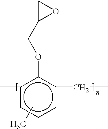
- another multi-functional reactive compound that may be employed to form primer layer 45 in the presence of formation 50 being formed from BULK MATERIAL includes an aromatic compound available from Schenectady International, Inc. in Schenectady, N.Y. under the product name ISORAD® 501.
- the X′ functional group 82 provides carboxylic functionality.
- the X functional group 84 provides acrylate functionality.
- Functional groups 82 and 84 are coupled to opposing ends of a backbone component 86 .
- ISORAD® 501 may have Structure A or B shown below, or a similar structure.
- x and y are integers indicating a number of repeating units.
- the repeating units may be randomly distributed.
- the high molecular weights of Structures A and B contributes to the mechanical strength build up of the adhesion layer.
- the polymeric backbones of Structures A and B if extended linearly, are in a range of about 2 nm to about 4 nm.
- functional group X may generate radicals that function to facilitate polymerization of the composition from which formation 50 is formed during solidification of the same.
- the functional group X would facilitate polymerization of formation 50 upon exposure to actinic energy, e.g., broad band ultraviolet energy.
- actinic energy e.g., broad band ultraviolet energy.
- An exemplary multi-functional reactive compound that includes these properties is a photo-initiator available from Ciba Specialty Chemicals in Tarrytown, N.Y. under the tradename IRGACURE® 2959 and has the following structure:
- the X′ functional group 90 provides hydroxyl functionality.
- the X functional group 92 provides initiator-type functionality. Specifically, in response to exposure to broad band ultraviolet energy the functional group X undergoes alpha-cleavage to generate benzoyl type of radicals. The radicals facilitate radical polymerization of the composition from which formation 50 is formed.
- Functional groups 90 and 92 are coupled to opposing ends of a backbone component 94 .
- compositions were formed including some of the aforementioned the multi-functional reactive compounds to determine the adhering strength of interfaces 66 and 68 .
- An exemplary composition including a multi-functional reactive compound is as follows:
- ⁇ -CEA was replaced by a cross-linking agent, a catalyst and ISORAD® 501.
- Both the cross-linking agent and catalyst is sold by Cytec Industries, Inc. of West Patterson, N.J.
- the cross-linking agent is sold under the product name CYMELTM 303ULF.
- a component of CYMELTM 303ULF is hexamethoxymethyl-melamine (HMMM).
- HMMM hexamethoxymethyl-melamine
- the methoxyl functional groups of HMMM can participate in many condensation reactions.
- the catalyst is sold under the product name CYCAT® 4040 providing the following composition:
- composition that may be employed as the multi-functional reactive compound omits DUV30J-16.
- the composition is as follows:
- Composition 3 includes approximately 77 grams of ISORAD® 501, 22 grams of CYMELTM 303ULF and one gram of CYCAT® 4040.
- ISORAD® 501, CYMELTM 303ULF and CYCAT® 4040 are combined.
- the combination of ISORAD® 501, CYMELTM 303ULF and CYCAT® 4040 are then introduced into approximately 1900 grams of PM Acetate.
- PM Acetate is a product name of a solvent consisting of 2-(1-methoxy)propyl acetate sold by Eastman Chemical Company of Kingsport, Tenn.
- COMPOSITION 4 similar to COMPOSITION 3, includes approximately 85.2 grams of ISORAD® 501, 13.8 grams of CYMELTM 303ULF and one gram of CYCAT® 4040.
- ISORAD® 501, CYMELTM 303ULF and CYCAT® 4040 are combined.
- the combination of ISORAD® 501, CYMELTM 303ULF and CYCAT® 4040 are then introduced into approximately 1900 grams of PM Acetate.
- COMPOSITION 5 similar to COMPOSITION 3, includes approximately 81 grams of ISORAD® 501, 18 grams of CYMELTM 303ULF and one gram of CYCAT® 4040.
- ISORAD® 501, CYMELTM 303ULF and CYCAT® 4040 are combined.
- the combination of ISORAD® 501, CYMELTM 303ULF and CYCAT® 4040 are then introduced into approximately 1900 grams of PM Acetate.
- compositions discussed above with respect to primer layer 45 are deposited upon substrate 42 employing spin-coating techniques wherein the substrate is rotated at a velocity between 500 and 4,000 revolutions per minute so as to provide a substantially smooth, if not planar layer with uniform thickness. This is followed by exposing the compositions to thermal actinic energy of 180° C. (Celsius) for approximately two minutes.
- compositions described above, COMPOSITIONs 1-5 were employed, along with IMPRINTING MATERIAL, to generate comparative data of the strength of the adhesion forces of interfaces 66 and 68 which was compared against baseline measuring of a primer layer 45 formed entirely from DUV30J-16, which is not known to form covalent bonds with formation 50 formed from IMPRINTING MATERIAL.
- formation 50 formed from BULK IMPRINTING MATERIAL
- primer layer 45 formed from COMPOSITIONS 1-5 and the base line COMPOSITION, were deposited and then solidified between two glass slides (not shown). Each glass slide (not shown) is approximately 1 mm thick, 75 ⁇ 25 mm in the lateral dimension.
- the glass slides (not shown) are subsequently rinsed with de-ionized water, sprayed with isopropyl alcohol, and exposed to a stream of fluid for drying, e.g., a stream of nitrogen gas. Thereafter, the glass slides (not shown) are baked at 120° C. (Celsius) for 2 hours.
- Primer layer 45 is deposited onto each of the two glass slides (not shown) employing spin-on techniques with a spin speed up to 3000 rpm. Primer layer 45 is lying on the glass slides (not shown) on hot plates at 180 C for 2 minutes.
- each of COMPOSITIONs 1-5, as well as the baseline composition are solidified, i.e., polymerized and cross-linked, by exposure to thermal energy. Formation is formed employing drop dispense techniques mentioned above. Specifically, BULK IMPRINTING MATERIAL is disposed as a plurality of droplets onto primer layer 45 on one of the two glass slides.
- the BULK IMPRINTING MATERIAL is then sandwiched between two primer layers 45 by having the primer layer on the two glass slides (not shown) facing one another and contacting BULK IMPRINTING MATERIAL.
- a longitudinal axis of one of the two glass slides (not shown) extends orthogonally to the longitudinal axis of the remaining glass slide (not shown).
- the BULK IMPRINTING MATERIAL is solidified, i.e., polymerized, and cross-linked by exposing the two glass slides (not shown) to actinic energy, such as broad band ultraviolet wavelengths, using a medium pressure mercury UV lamp for 40 seconds at 20 mW/cm 2 intensity.
- COMPOSITION 6 a low-solids composition similar to COMPOSITION 5, includes 0.81 grams of ISORAD® 501, 0.18 grams CYMELTM 303ULF, 0.01 grams CYCAT® 4040, and 1999 grams PM Acetate.
- COMPOSITION 6 may be cast onto a wafer and spun to form a film. During a spinning process, solvent evaporates, and a thin, solid film is formed on the surface. The percentage of dissolved solids in the composition and the spin coating speed may be adjusted to achieve a desired film thickness on a substrate or wafer. After spin-coating, the adhesion layer may be cured, for example, by contact baking on a hot plate at 150° C. for about 1 minute.
- FIGS. 12A and 12B illustrate measurement locations 1200 of polymeric adhesion layer thickness for COMPOSITION 6 applied as described above to an 8′′ silicon wafer with a spin rate of 1000 rpm.
- Solid film thickness measurements of the sample were performed by spectroscopic reflectometry with optical metrology systems available from Metrosol, Inc., Austin, Tex.
- the mean layer thickness was determined to be 1.09 nm, with a maximum measured thickness of 1.22 nm, a minimum measured thickness of 0.94 nm, and a standard deviation of 0.05 nm.
- the mean layer thickness was determined, using model VUV-7000, to be 1.01 nm, with a maximum measured thickness of 1.07 nm, a minimum measured thickness of 0.95 nm, and a standard deviation of 0.03 nm.
- FIG. 13 is a scanning electron micrograph (SEM) image of polymeric adhesion layer 1300 formed from COMPOSITION 6 between the silicon oxide surface on a silicon wafer 1302 and an acrylate imprint resist 1304 .
- Polymeric adhesion layer 1300 is about 1 nm thick. Testing indicated that the 1-nm-thick polymeric adhesion layer achieves adhesion strength similar to that of a polymeric adhesion layer of a similar composition with a much greater thickness (e.g., greater than about 6 nm). That is, polymeric adhesion layer 1300 does not exhibit cohesive failure under the tensile load applied during template separation.
- a polymeric adhesion layer composition including polymeric components with an extended backbone length greater than about 2 nm (e.g., in a range of about 2 nm to about 4 nm) was shown to form a polymeric adhesion layer with thickness of less than about 2 nm (e.g., about 1 nm).
- the polymeric components are thought to be aligned during spin-coating such that backbones of the polymeric components are “lying down” on (or more parallel with) the surface of the substrate rather than “standing up” on (or more perpendicular to) the surface of the substrate.
- the polymeric components, aligned with respect to the surface of the substrate in this way, are thought to be in a planar configuration on the surface of the substrate, with the longer dimensions of the polymeric components generally extended along the surface of the substrate and forming an ultra-thin layer on the substrate.
- This ultra-thin polymeric adhesion layer demonstrates adhesive strength generally thought to be associated with adhesion layers of much greater thickness, and allows reduction of the overall thickness of imprinting stacks for nano-imprint lithography.
- the solvent PM Acetate is employed primarily to dissolve the other constituent components of COMPOSITIONs 3, 4 and 5.
- many common photo-resist solvents may be employed in lieu of PM Acetate, such as diethylene glycol monoethyl ether acetate, methyl amyl ketone or the like.
- the solid contents of COMPOSITIONs 3, 4 and 5, i.e., ISORAD® 501, CYMELTM 303ULF and CYCAT® 4040 may comprise between 0.1% to 70% of the composition, weight, and more preferably in a range of 0.5% to 10% by weight, with the remaining quantity consisting of the solvent.
- the solid component of each of COMPOSITIONs 3, 4, and 5 may comprise 50% to 99%, by weight of ISORAD® 501, 1% to 50%, by weight of CYMELTM 303ULF and 0% to 10% by weight of CYCAT® 4040.
Abstract
Description
-
- isobornyl acrylate
- n-hexyl acrylate
- ethylene glycol diacrylate
- 2-hydroxy-2-methyl-1-phenyl-propan-1-one

and comprises approximately 47% of bulk material by weight, but may be present in a range of 20% to 80%, inclusive. As a result, the mechanical properties of
and comprises approximately 25% of bulk material by weight, but may be present in a range of 0% to 50%, inclusive. Also providing flexibility to

and comprises approximately 25% of bulk material by weight, and may be present in a range of 10% to 50%, inclusive. EGDA also contributes to the modulus and stiffness buildup, as well as facilitates cross-linking of n-HA and IBOA during polymerization of the bulk material.

and comprises approximately 3% of the bulk material by weight, and may be present in a range of 1% to 5%, inclusive. The actinic energy to which the initiator is responsive is broad band ultra-violet energy generated by a medium-pressure mercury lamp. In this manner, the initiator facilitates cross-linking and polymerization of the components of the bulk material.

In which R, R′, R″ and R′″ are linking groups and x, y, z are averaged repeating numbers of the groups associated therewith. These repeating units could be randomly distributed. The groups X and X′ denote the functional groups, with the understanding that typically, the functional group X differs from functional group X′. One of the functional groups X and X′, for example X′, is selected to achieve cross-reaction with the material from which

The X′

In Structures A and B, x and y are integers indicating a number of repeating units. The repeating units may be randomly distributed.
The X′
-
- β-CEA
- DUV30J-16
where DUV30J-16 comprises approximately 100 grams ofcomposition 1 and β-CEA comprises approximately 0.219 grams. DUV30J-16 is a bottom anti-reflective coating (BARC) available from Brewer Science in Rolla, Mo. containing 93% solvent, and 7% non-solvent reactive components. DUV30J-16 contains phenolic resins, and its crosslinker can react with carboxylic functional group. It is believed that DUV30J-16 will not form covalent bonds withformation 50.
-
- DUV30J-16
- ISORAD® 501
- CYMEL™ 303ULF
- CYCAT® 4040
Approximately 100 grams of COMPOSITION 2 comprises DUV30J-16, 0.611 gram of COMPOSITION 2 comprises ISORAD® 501, 0.175 gram of COMPOSITION 2 comprises CYMEL™ 303ULF and 0.008 gram of COMPOSITION 2 comprises CYCAT® 4040.
-
- ISORAD® 501
- CYMEL™ 303ULF
- CYCAT® 4040
- PM Acetate
Claims (17)
Priority Applications (5)
| Application Number | Priority Date | Filing Date | Title |
|---|---|---|---|
| US12/326,709 US8846195B2 (en) | 2005-07-22 | 2008-12-02 | Ultra-thin polymeric adhesion layer |
| KR1020107013979A KR101610185B1 (en) | 2007-12-04 | 2008-12-04 | Ultra-thin polymeric adhesion layer |
| PCT/US2008/013352 WO2009085090A1 (en) | 2007-12-04 | 2008-12-04 | Ultra-thin polymeric adhesion layer |
| EP08866379A EP2217968A4 (en) | 2007-12-04 | 2008-12-04 | Ultra-thin polymeric adhesion layer |
| JP2010536928A JP5406204B2 (en) | 2007-12-04 | 2008-12-04 | Ultra-thin polymer adhesive layer |
Applications Claiming Priority (5)
| Application Number | Priority Date | Filing Date | Title |
|---|---|---|---|
| US11/187,406 US7759407B2 (en) | 2005-07-22 | 2005-07-22 | Composition for adhering materials together |
| US11/187,407 US8557351B2 (en) | 2005-07-22 | 2005-07-22 | Method for adhering materials together |
| US11/734,542 US8808808B2 (en) | 2005-07-22 | 2007-04-12 | Method for imprint lithography utilizing an adhesion primer layer |
| US99217907P | 2007-12-04 | 2007-12-04 | |
| US12/326,709 US8846195B2 (en) | 2005-07-22 | 2008-12-02 | Ultra-thin polymeric adhesion layer |
Related Parent Applications (1)
| Application Number | Title | Priority Date | Filing Date |
|---|---|---|---|
| US11/187,406 Continuation-In-Part US7759407B2 (en) | 2005-07-22 | 2005-07-22 | Composition for adhering materials together |
Publications (2)
| Publication Number | Publication Date |
|---|---|
| US20090155583A1 US20090155583A1 (en) | 2009-06-18 |
| US8846195B2 true US8846195B2 (en) | 2014-09-30 |
Family
ID=40824588
Family Applications (1)
| Application Number | Title | Priority Date | Filing Date |
|---|---|---|---|
| US12/326,709 Active 2029-03-14 US8846195B2 (en) | 2005-07-22 | 2008-12-02 | Ultra-thin polymeric adhesion layer |
Country Status (5)
| Country | Link |
|---|---|
| US (1) | US8846195B2 (en) |
| EP (1) | EP2217968A4 (en) |
| JP (1) | JP5406204B2 (en) |
| KR (1) | KR101610185B1 (en) |
| WO (1) | WO2009085090A1 (en) |
Cited By (12)
| Publication number | Priority date | Publication date | Assignee | Title |
|---|---|---|---|---|
| EP3141956A1 (en) | 2015-09-08 | 2017-03-15 | Canon Kabushiki Kaisha | Substrate pretreatment for reducing fill time in nanoimprint lithography |
| US9773672B2 (en) | 2015-02-09 | 2017-09-26 | Samsung Electronics Co., Ltd. | Method of forming micropatterns |
| US10095106B2 (en) | 2016-03-31 | 2018-10-09 | Canon Kabushiki Kaisha | Removing substrate pretreatment compositions in nanoimprint lithography |
| US10134588B2 (en) | 2016-03-31 | 2018-11-20 | Canon Kabushiki Kaisha | Imprint resist and substrate pretreatment for reducing fill time in nanoimprint lithography |
| US10317793B2 (en) | 2017-03-03 | 2019-06-11 | Canon Kabushiki Kaisha | Substrate pretreatment compositions for nanoimprint lithography |
| US10488753B2 (en) | 2015-09-08 | 2019-11-26 | Canon Kabushiki Kaisha | Substrate pretreatment and etch uniformity in nanoimprint lithography |
| US10509313B2 (en) | 2016-06-28 | 2019-12-17 | Canon Kabushiki Kaisha | Imprint resist with fluorinated photoinitiator and substrate pretreatment for reducing fill time in nanoimprint lithography |
| US10578965B2 (en) * | 2016-03-31 | 2020-03-03 | Canon Kabushiki Kaisha | Pattern forming method |
| US10620539B2 (en) | 2016-03-31 | 2020-04-14 | Canon Kabushiki Kaisha | Curing substrate pretreatment compositions in nanoimprint lithography |
| US10754244B2 (en) | 2016-03-31 | 2020-08-25 | Canon Kabushiki Kaisha | Pattern forming method as well as production methods for processed substrate, optical component, circuit board, electronic component and imprint mold |
| US10829644B2 (en) | 2016-03-31 | 2020-11-10 | Canon Kabushiki Kaisha | Pattern forming method as well as production methods for processed substrate, optical component, circuit board, electronic component and imprint mold |
| US10883006B2 (en) | 2016-03-31 | 2021-01-05 | Canon Kabushiki Kaisha | Pattern forming method as well as production methods for processed substrate, optical component, circuit board, electronic component and imprint mold |
Families Citing this family (30)
| Publication number | Priority date | Publication date | Assignee | Title |
|---|---|---|---|---|
| US7307118B2 (en) * | 2004-11-24 | 2007-12-11 | Molecular Imprints, Inc. | Composition to reduce adhesion between a conformable region and a mold |
| US8557351B2 (en) * | 2005-07-22 | 2013-10-15 | Molecular Imprints, Inc. | Method for adhering materials together |
| US8846195B2 (en) | 2005-07-22 | 2014-09-30 | Canon Nanotechnologies, Inc. | Ultra-thin polymeric adhesion layer |
| US7759407B2 (en) | 2005-07-22 | 2010-07-20 | Molecular Imprints, Inc. | Composition for adhering materials together |
| US8808808B2 (en) * | 2005-07-22 | 2014-08-19 | Molecular Imprints, Inc. | Method for imprint lithography utilizing an adhesion primer layer |
| US8361546B2 (en) * | 2008-10-30 | 2013-01-29 | Molecular Imprints, Inc. | Facilitating adhesion between substrate and patterned layer |
| JP5583374B2 (en) * | 2009-09-07 | 2014-09-03 | 株式会社島津製作所 | Photo-curing resin characteristic testing device, holder used in the testing device, and characteristic testing method |
| US20110165412A1 (en) * | 2009-11-24 | 2011-07-07 | Molecular Imprints, Inc. | Adhesion layers in nanoimprint lithograhy |
| JP5218521B2 (en) | 2010-10-21 | 2013-06-26 | 大日本印刷株式会社 | Imprint method and transfer substrate and adhesive used therefor |
| WO2013051735A1 (en) * | 2011-10-07 | 2013-04-11 | Fujifilm Corporation | Underlay film composition for imprints and method of forming pattern and pattern formation method using the same |
| JP5767615B2 (en) * | 2011-10-07 | 2015-08-19 | 富士フイルム株式会社 | Underlayer film composition for imprint and pattern forming method using the same |
| JP5899145B2 (en) * | 2012-06-18 | 2016-04-06 | 富士フイルム株式会社 | Composition for forming underlayer film for imprint and pattern forming method |
| JP5827180B2 (en) * | 2012-06-18 | 2015-12-02 | 富士フイルム株式会社 | Imprint curable composition and substrate adhesion composition, and semiconductor device using the same |
| US20150298387A1 (en) * | 2012-12-05 | 2015-10-22 | Japan Science And Technology Agency | Resin for nanoimprinting, laminate containing resin for nanoimprinting, printed board containing resin for nanoimprinting, and method for producing nanoimprint substrate |
| JP6029506B2 (en) * | 2013-03-26 | 2016-11-24 | 富士フイルム株式会社 | Composition for forming underlayer film for imprint and pattern forming method |
| KR102056902B1 (en) * | 2013-05-29 | 2019-12-18 | 삼성전자주식회사 | Wire grid polarizer and liquid crystal display panel and liquid crystal display device having the same |
| KR102089661B1 (en) | 2013-08-27 | 2020-03-17 | 삼성전자주식회사 | Wire grid polarizer and liquid crystal display panel and liquid crystal display device having the same |
| TWI632188B (en) | 2014-08-27 | 2018-08-11 | 日商富士軟片股份有限公司 | Underlayer film forming resin composition, laminated body, pattern forming method, imprint forming kit and element manufacturing method |
| JP6141500B2 (en) * | 2015-09-08 | 2017-06-07 | キヤノン株式会社 | Substrate pretreatment to reduce filling time in nanoimprint lithography |
| US10042253B2 (en) * | 2016-01-11 | 2018-08-07 | Samsung Display Co., Ltd. | Photosensitive resin composition, film prepared by using the photosensitive resin composition, and organic light-emitting display device including the film |
| KR20170084681A (en) * | 2016-01-11 | 2017-07-20 | 삼성디스플레이 주식회사 | Photosensitive resin composition, film prepared the composition, and organic light emitting display device comprising the film |
| TW201817582A (en) * | 2016-09-16 | 2018-05-16 | 日商富士軟片股份有限公司 | Pattern forming method and method for producing semiconductor element |
| TW201825617A (en) * | 2016-09-16 | 2018-07-16 | 日商富士軟片股份有限公司 | Composition for forming primer layer for imprinting, primer layer for imprinting, and laminate |
| WO2018159575A1 (en) | 2017-02-28 | 2018-09-07 | 富士フイルム株式会社 | Composition for forming imprint adhesive film, adhesive film, laminate, method for producing cured material pattern, and method of manufacturing circuit board |
| WO2018159576A1 (en) * | 2017-02-28 | 2018-09-07 | 富士フイルム株式会社 | Primer layer-forming composition, kit, primer layer, and laminate. |
| KR102393376B1 (en) | 2017-04-10 | 2022-05-03 | 삼성디스플레이 주식회사 | Photosensitive resin composition, and electronic device comprising cured product of composition for forming pattern comprising the same |
| TW201900704A (en) | 2017-04-11 | 2019-01-01 | 日商富士軟片股份有限公司 | Composition, adhesion film, laminate, method for producing cured pattern, and method for manufacturing circuit board |
| JP6982623B2 (en) * | 2017-09-26 | 2021-12-17 | 富士フイルム株式会社 | Underlayer film forming composition for imprint, kit, curable composition for imprint, laminate, manufacturing method of laminate, manufacturing method of cured product pattern, manufacturing method of circuit board |
| EP3704197A1 (en) * | 2017-10-31 | 2020-09-09 | 3M Innovative Properties Company | Interfacial adhesion article and method |
| US10780682B2 (en) | 2018-12-20 | 2020-09-22 | Canon Kabushiki Kaisha | Liquid adhesion composition, multi-layer structure and method of making said structure |
Citations (86)
| Publication number | Priority date | Publication date | Assignee | Title |
|---|---|---|---|---|
| US3498827A (en) * | 1966-02-02 | 1970-03-03 | Exxon Research Engineering Co | Abrasion resistant metal articles |
| US4506003A (en) | 1980-06-21 | 1985-03-19 | Hoechst Aktiengesellschaft | Positive-working radiation-sensitive mixture |
| JPS6140845Y2 (en) | 1981-07-31 | 1986-11-20 | ||
| WO1991004151A1 (en) | 1989-09-14 | 1991-04-04 | Avery International Corporation | Tackified dual cure pressure-sensitive adhesive |
| JPH04330650A (en) | 1991-05-01 | 1992-11-18 | Dainippon Ink & Chem Inc | Production of substrate for optical disk |
| EP0592139A1 (en) | 1992-10-06 | 1994-04-13 | Ciba-Geigy Ag | Composition for priming and cleaning based on organosilane |
| EP0592972A2 (en) | 1992-10-13 | 1994-04-20 | INSTITUT FÜR MIKROTECHNIK MAINZ GmbH | Resist coated metal- or semiconductor-substrate having a stable resist-substrate adhesion |
| US5368942A (en) | 1993-01-15 | 1994-11-29 | The United States Of America As Represented By The Secreatary Of Commerce | Method of adhering substrates |
| US5432700A (en) | 1992-12-21 | 1995-07-11 | Ford Motor Company | Adaptive active vehicle suspension system |
| US5458953A (en) | 1991-09-12 | 1995-10-17 | Mannington Mills, Inc. | Resilient floor covering and method of making same |
| WO1996000656A1 (en) | 1994-06-30 | 1996-01-11 | Elf Atochem S.A. | Packaging material including a silica layer and a polyolefin layer |
| US5545367A (en) | 1992-04-15 | 1996-08-13 | Soane Technologies, Inc. | Rapid prototype three dimensional stereolithography |
| JPH08208781A (en) | 1994-11-09 | 1996-08-13 | Shell Internatl Res Maatschappij Bv | Low-viscosity adhesive composition containing asymmetric radial polymer |
| US5578683A (en) | 1994-06-27 | 1996-11-26 | Avery Dennison Corporation | Crosslinkable graft pressure-sensitive adhesives |
| US5750753A (en) | 1996-01-24 | 1998-05-12 | Chisso Corporation | Method for manufacturing acryloxypropysilane |
| US5942302A (en) | 1996-02-23 | 1999-08-24 | Imation Corp. | Polymer layer for optical media |
| WO2001063605A1 (en) | 2000-02-22 | 2001-08-30 | Krauss-Maffei Kunststofftechnik Gmbh | Method and device for producing a dvd |
| JP2002060529A (en) | 2000-08-22 | 2002-02-26 | Fuji Photo Film Co Ltd | High-adhesion hard coated film |
| US20020094496A1 (en) | 2000-07-17 | 2002-07-18 | Choi Byung J. | Method and system of automatic fluid dispensing for imprint lithography processes |
| US20020123592A1 (en) | 2001-03-02 | 2002-09-05 | Zenastra Photonics Inc. | Organic-inorganic hybrids surface adhesion promoter |
| JP2002285071A (en) | 2001-03-26 | 2002-10-03 | Riken Technos Corp | Anchor-coat agent, easily-adhesive base film and laminated film |
| JP2002355543A (en) | 2001-01-25 | 2002-12-10 | Sekisui Chem Co Ltd | Dispersant, heat developable photosensitive material, ceramic green sheet, primer for plastic lens, recording agent for water base ink and adhesive for metallic foil |
| US20030017368A1 (en) | 1999-05-07 | 2003-01-23 | Junhua Wu | Elastomeric lubricants for magnetic recording media |
| US6518168B1 (en) | 1995-08-18 | 2003-02-11 | President And Fellows Of Harvard College | Self-assembled monolayer directed patterning of surfaces |
| US6610458B2 (en) | 2001-07-23 | 2003-08-26 | Kodak Polychrome Graphics Llc | Method and system for direct-to-press imaging |
| WO2003087935A2 (en) | 2002-04-17 | 2003-10-23 | Clariant Gmbh | Nanoimprint resist |
| US6667082B2 (en) | 1997-01-21 | 2003-12-23 | Cryovac, Inc. | Additive transfer film suitable for cook-in end use |
| US20030235787A1 (en) | 2002-06-24 | 2003-12-25 | Watts Michael P.C. | Low viscosity high resolution patterning material |
| JP2004051706A (en) | 2002-07-17 | 2004-02-19 | Fuji Photo Film Co Ltd | Hard coat-treated article and method for producing the same |
| US20040037956A1 (en) | 2002-08-22 | 2004-02-26 | Eastman Kodak Company | Method of coating micro-electromechanical devices |
| WO2004021083A1 (en) | 2002-08-27 | 2004-03-11 | Obducat Ab | Device for transferring a pattern to an object |
| DE10237280A1 (en) | 2002-08-14 | 2004-03-11 | Micronas Holding Gmbh | Process for connecting surfaces, semiconductors with bonded surfaces as well as bio-chip and bio-sensor |
| US20040065976A1 (en) | 2002-10-04 | 2004-04-08 | Sreenivasan Sidlgata V. | Method and a mold to arrange features on a substrate to replicate features having minimal dimensional variability |
| US20040065252A1 (en) | 2002-10-04 | 2004-04-08 | Sreenivasan Sidlgata V. | Method of forming a layer on a substrate to facilitate fabrication of metrology standards |
| US6719915B2 (en) | 1999-03-11 | 2004-04-13 | Board Of Regents, The University Of Texas System | Step and flash imprint lithography |
| US6720076B2 (en) | 2002-05-31 | 2004-04-13 | Omnova Solutions Inc. | In-mold primer coating for thermoplastic substrates |
| US20040110096A1 (en) | 2001-04-10 | 2004-06-10 | Takahiro Kishioka | Composition for forming antireflection film for lithography |
| US20040116548A1 (en) | 2002-12-12 | 2004-06-17 | Molecular Imprints, Inc. | Compositions for dark-field polymerization and method of using the same for imprint lithography processes |
| US20040127613A1 (en) | 2002-12-11 | 2004-07-01 | Shin-Etsu Chemical Co., Ltd. | Radiation curing silicone rubber composition, adhesive silicone elastomer film formed from same, semiconductor device using same, and method of producing semiconductor device |
| US20040124566A1 (en) | 2002-07-11 | 2004-07-01 | Sreenivasan Sidlgata V. | Step and repeat imprint lithography processes |
| US20040157078A1 (en) | 2001-01-25 | 2004-08-12 | Takahiro Yoshida | Polyvinyl acetal, polyvinyl acetal composition, ink coating material, dispersant, heat-developable photosensitive material,ceramic green sheet, primer for plastic lens, recording agent for water-based ink and adhesive for metal foil |
| US20040168613A1 (en) | 2003-02-27 | 2004-09-02 | Molecular Imprints, Inc. | Composition and method to form a release layer |
| US20040175631A1 (en) | 2002-10-21 | 2004-09-09 | Nanoink, Inc. | Nanometer-scale engineered structures, methods and apparatus for fabrication thereof, and applications to mask repair, enhancement, and fabrications |
| US20040188381A1 (en) | 2003-03-25 | 2004-09-30 | Molecular Imprints, Inc. | Positive tone bi-layer imprint lithography method |
| US20040191429A1 (en) | 1999-08-17 | 2004-09-30 | Western Washington University | Liquid crystal imprinting |
| US20040211754A1 (en) | 2003-04-25 | 2004-10-28 | Molecular Imprints, Inc. | Method of forming stepped structures employing imprint lithography |
| US20040259992A1 (en) | 2001-01-26 | 2004-12-23 | Roland Gobel | Adhesives for metal-polymer composites |
| US6873087B1 (en) | 1999-10-29 | 2005-03-29 | Board Of Regents, The University Of Texas System | High precision orientation alignment and gap control stages for imprint lithography processes |
| US20050098534A1 (en) | 2003-11-12 | 2005-05-12 | Molecular Imprints, Inc. | Formation of conductive templates employing indium tin oxide |
| EP1533657A1 (en) | 2003-11-21 | 2005-05-25 | Obducat AB | Multilayer nano imprint lithography |
| US20050160934A1 (en) | 2004-01-23 | 2005-07-28 | Molecular Imprints, Inc. | Materials and methods for imprint lithography |
| US6932934B2 (en) | 2002-07-11 | 2005-08-23 | Molecular Imprints, Inc. | Formation of discontinuous films during an imprint lithography process |
| US20050187339A1 (en) | 2004-02-23 | 2005-08-25 | Molecular Imprints, Inc. | Materials for imprint lithography |
| US6936194B2 (en) | 2002-09-05 | 2005-08-30 | Molecular Imprints, Inc. | Functional patterning material for imprint lithography processes |
| US6957608B1 (en) | 2002-08-02 | 2005-10-25 | Kovio, Inc. | Contact print methods |
| US20060030071A1 (en) | 2004-08-05 | 2006-02-09 | Fujitsu Limited | Method for processing base |
| US20060030653A1 (en) | 2004-08-04 | 2006-02-09 | Xerox Corporation | Polycarbonates and photoconductive imaging members |
| US20060029811A1 (en) | 2004-08-06 | 2006-02-09 | Nippon Shokubai Co., Ltd. | Resin composition, method of its composition, and cured formulation |
| US20060046069A1 (en) | 2004-08-30 | 2006-03-02 | Jung Gun Y | Increasing adhesion in an imprinting procedure |
| US7011932B2 (en) | 2001-05-01 | 2006-03-14 | E. I. Du Pont De Nemours And Company | Polymer waveguide fabrication process |
| US20060062922A1 (en) | 2004-09-23 | 2006-03-23 | Molecular Imprints, Inc. | Polymerization technique to attenuate oxygen inhibition of solidification of liquids and composition therefor |
| US20060081557A1 (en) | 2004-10-18 | 2006-04-20 | Molecular Imprints, Inc. | Low-k dielectric functional imprinting materials |
| US20060108710A1 (en) | 2004-11-24 | 2006-05-25 | Molecular Imprints, Inc. | Method to reduce adhesion between a conformable region and a mold |
| US20060145398A1 (en) | 2004-12-30 | 2006-07-06 | Board Of Regents, The University Of Texas System | Release layer comprising diamond-like carbon (DLC) or doped DLC with tunable composition for imprint lithography templates and contact masks |
| US20060188751A1 (en) | 2005-02-24 | 2006-08-24 | Tdk Corporation | Magnetic recording medium and magnetic recording/reproducing device |
| US20060222897A1 (en) | 2005-03-30 | 2006-10-05 | Kabushiki Kaisha Toshiba | Discrete track media and method of manufacturing the same |
| US7141188B2 (en) | 2001-05-30 | 2006-11-28 | Honeywell International Inc. | Organic compositions |
| US20060279024A1 (en) | 2003-06-17 | 2006-12-14 | Molecular Imprints, Inc. | Method for providing desirable wetting and release characteristics between a mold and a polymerizable composition |
| US7163888B2 (en) | 2004-11-22 | 2007-01-16 | Motorola, Inc. | Direct imprinting of etch barriers using step and flash imprint lithography |
| US20070021520A1 (en) | 2005-07-22 | 2007-01-25 | Molecular Imprints, Inc. | Composition for adhering materials together |
| US20070017631A1 (en) | 2005-07-22 | 2007-01-25 | Molecular Imprints, Inc. | Method for adhering materials together |
| US20070042173A1 (en) | 2005-08-22 | 2007-02-22 | Fuji Photo Film Co., Ltd. | Antireflection film, manufacturing method thereof, and polarizing plate using the same, and image display device |
| US20070051697A1 (en) | 2005-09-02 | 2007-03-08 | Dipietro Richard A | Processes and materials for step and flash imprint lithography |
| US20070059211A1 (en) | 2005-03-11 | 2007-03-15 | The College Of Wooster | TNT sensor containing molecularly imprinted sol gel-derived films |
| US20070212494A1 (en) | 2005-07-22 | 2007-09-13 | Molecular Imprints, Inc. | Method for Imprint Lithography Utilizing an Adhesion Primer Layer |
| US20070272825A1 (en) | 2004-01-23 | 2007-11-29 | Molecular Imprints, Inc. | Composition to Reduce Adhesion Between a Conformable Region and a Mold |
| US7309225B2 (en) | 2004-08-13 | 2007-12-18 | Molecular Imprints, Inc. | Moat system for an imprint lithography template |
| US20080110557A1 (en) | 2006-11-15 | 2008-05-15 | Molecular Imprints, Inc. | Methods and Compositions for Providing Preferential Adhesion and Release of Adjacent Surfaces |
| US20080131623A1 (en) | 2006-11-28 | 2008-06-05 | Wei Zhang | Method and apparatus to apply surface release coating for imprint mold |
| US7393789B2 (en) | 2005-09-01 | 2008-07-01 | Micron Technology, Inc. | Protective coating for planarization |
| US20090136654A1 (en) | 2005-10-05 | 2009-05-28 | Molecular Imprints, Inc. | Contact Angle Attenuations on Multiple Surfaces |
| WO2009085090A1 (en) | 2007-12-04 | 2009-07-09 | Molecular Imprints, Inc. | Ultra-thin polymeric adhesion layer |
| US20090197057A1 (en) | 2008-02-05 | 2009-08-06 | Molecular Imprints, Inc. | Controlling Template Surface Composition in Nano-Imprint Lithography |
| JP4330650B2 (en) | 2005-06-03 | 2009-09-16 | 中 奥村 | Medication support program |
| WO2010051024A1 (en) | 2008-10-30 | 2010-05-06 | Molecular Imprints, Inc. | Facilitating adhesion between substrate and patterned layer |
| US20110165412A1 (en) | 2009-11-24 | 2011-07-07 | Molecular Imprints, Inc. | Adhesion layers in nanoimprint lithograhy |
Family Cites Families (19)
| Publication number | Priority date | Publication date | Assignee | Title |
|---|---|---|---|---|
| US62867A (en) * | 1867-03-12 | Donald l | ||
| US29811A (en) * | 1860-08-28 | Qtjilting-eb | ||
| US81557A (en) * | 1868-08-25 | Leonard s | ||
| US224452A (en) * | 1880-02-10 | Uterine supporter | ||
| US42173A (en) * | 1864-04-05 | Improvement in grain-cradles | ||
| US127613A (en) * | 1872-06-04 | Improvement in plows | ||
| US65252A (en) * | 1867-05-28 | Improved paddle-wheel | ||
| US175631A (en) * | 1876-04-04 | Improvement in soap | ||
| US65976A (en) * | 1867-06-18 | Thomas w | ||
| US17631A (en) * | 1857-06-23 | Thomas mitchell | ||
| US94496A (en) * | 1869-09-07 | Improved animal-trap | ||
| US123592A (en) * | 1872-02-13 | strong | ||
| US212494A (en) * | 1879-02-18 | Improvement in bottle-fillers | ||
| US21520A (en) * | 1858-09-14 | Spring-balance in combination with a knife | ||
| US59211A (en) * | 1866-10-30 | Improved gate-hinge | ||
| GB0324785D0 (en) * | 2003-10-24 | 2003-11-26 | Electronica Products Ltd | Magnetic gearing of permanent magnet brushless motors |
| US20060110557A1 (en) * | 2004-09-03 | 2006-05-25 | Zhiyong Xia | Polyester polymer and copolymer compositions containing metallic tungsten particles |
| JP2007080367A (en) * | 2005-09-13 | 2007-03-29 | Toshiba Corp | Information storage medium, information recording method and information reproducing apparatus |
| US7998651B2 (en) * | 2006-05-15 | 2011-08-16 | Asml Netherlands B.V. | Imprint lithography |
-
2008
- 2008-12-02 US US12/326,709 patent/US8846195B2/en active Active
- 2008-12-04 WO PCT/US2008/013352 patent/WO2009085090A1/en active Application Filing
- 2008-12-04 JP JP2010536928A patent/JP5406204B2/en active Active
- 2008-12-04 EP EP08866379A patent/EP2217968A4/en not_active Withdrawn
- 2008-12-04 KR KR1020107013979A patent/KR101610185B1/en active IP Right Grant
Patent Citations (106)
| Publication number | Priority date | Publication date | Assignee | Title |
|---|---|---|---|---|
| US3498827A (en) * | 1966-02-02 | 1970-03-03 | Exxon Research Engineering Co | Abrasion resistant metal articles |
| US4506003A (en) | 1980-06-21 | 1985-03-19 | Hoechst Aktiengesellschaft | Positive-working radiation-sensitive mixture |
| JPS6140845Y2 (en) | 1981-07-31 | 1986-11-20 | ||
| KR0153746B1 (en) | 1989-09-14 | 1998-11-16 | 에드윈 씨.섬머스 | Tackified duke pressure sensitive adhesive |
| WO1991004151A1 (en) | 1989-09-14 | 1991-04-04 | Avery International Corporation | Tackified dual cure pressure-sensitive adhesive |
| JPH04330650A (en) | 1991-05-01 | 1992-11-18 | Dainippon Ink & Chem Inc | Production of substrate for optical disk |
| US5458953A (en) | 1991-09-12 | 1995-10-17 | Mannington Mills, Inc. | Resilient floor covering and method of making same |
| US5545367A (en) | 1992-04-15 | 1996-08-13 | Soane Technologies, Inc. | Rapid prototype three dimensional stereolithography |
| EP0592139A1 (en) | 1992-10-06 | 1994-04-13 | Ciba-Geigy Ag | Composition for priming and cleaning based on organosilane |
| EP0592972A2 (en) | 1992-10-13 | 1994-04-20 | INSTITUT FÜR MIKROTECHNIK MAINZ GmbH | Resist coated metal- or semiconductor-substrate having a stable resist-substrate adhesion |
| US5432700A (en) | 1992-12-21 | 1995-07-11 | Ford Motor Company | Adaptive active vehicle suspension system |
| US5368942A (en) | 1993-01-15 | 1994-11-29 | The United States Of America As Represented By The Secreatary Of Commerce | Method of adhering substrates |
| US5578683A (en) | 1994-06-27 | 1996-11-26 | Avery Dennison Corporation | Crosslinkable graft pressure-sensitive adhesives |
| JPH09502406A (en) | 1994-06-30 | 1997-03-11 | エルフ アトケム ソシエテ アノニム | Packaging material having silicon oxide layer and polyolefin layer |
| US5731092A (en) | 1994-06-30 | 1998-03-24 | Elf Atochem S.A. | Packaging material comprising a silicon oxide layer and a polyolefin layer |
| WO1996000656A1 (en) | 1994-06-30 | 1996-01-11 | Elf Atochem S.A. | Packaging material including a silica layer and a polyolefin layer |
| US5550196A (en) | 1994-11-09 | 1996-08-27 | Shell Oil Company | Low viscosity adhesive compositions containing asymmetric radial polymers |
| JPH08208781A (en) | 1994-11-09 | 1996-08-13 | Shell Internatl Res Maatschappij Bv | Low-viscosity adhesive composition containing asymmetric radial polymer |
| US6518168B1 (en) | 1995-08-18 | 2003-02-11 | President And Fellows Of Harvard College | Self-assembled monolayer directed patterning of surfaces |
| US5750753A (en) | 1996-01-24 | 1998-05-12 | Chisso Corporation | Method for manufacturing acryloxypropysilane |
| US5942302A (en) | 1996-02-23 | 1999-08-24 | Imation Corp. | Polymer layer for optical media |
| US6667082B2 (en) | 1997-01-21 | 2003-12-23 | Cryovac, Inc. | Additive transfer film suitable for cook-in end use |
| US6719915B2 (en) | 1999-03-11 | 2004-04-13 | Board Of Regents, The University Of Texas System | Step and flash imprint lithography |
| US20030017368A1 (en) | 1999-05-07 | 2003-01-23 | Junhua Wu | Elastomeric lubricants for magnetic recording media |
| US20040191429A1 (en) | 1999-08-17 | 2004-09-30 | Western Washington University | Liquid crystal imprinting |
| US6873087B1 (en) | 1999-10-29 | 2005-03-29 | Board Of Regents, The University Of Texas System | High precision orientation alignment and gap control stages for imprint lithography processes |
| WO2001063605A1 (en) | 2000-02-22 | 2001-08-30 | Krauss-Maffei Kunststofftechnik Gmbh | Method and device for producing a dvd |
| US20020094496A1 (en) | 2000-07-17 | 2002-07-18 | Choi Byung J. | Method and system of automatic fluid dispensing for imprint lithography processes |
| JP2002060529A (en) | 2000-08-22 | 2002-02-26 | Fuji Photo Film Co Ltd | High-adhesion hard coated film |
| US20040157078A1 (en) | 2001-01-25 | 2004-08-12 | Takahiro Yoshida | Polyvinyl acetal, polyvinyl acetal composition, ink coating material, dispersant, heat-developable photosensitive material,ceramic green sheet, primer for plastic lens, recording agent for water-based ink and adhesive for metal foil |
| JP2002355543A (en) | 2001-01-25 | 2002-12-10 | Sekisui Chem Co Ltd | Dispersant, heat developable photosensitive material, ceramic green sheet, primer for plastic lens, recording agent for water base ink and adhesive for metallic foil |
| US20040259992A1 (en) | 2001-01-26 | 2004-12-23 | Roland Gobel | Adhesives for metal-polymer composites |
| US20020123592A1 (en) | 2001-03-02 | 2002-09-05 | Zenastra Photonics Inc. | Organic-inorganic hybrids surface adhesion promoter |
| JP2002285071A (en) | 2001-03-26 | 2002-10-03 | Riken Technos Corp | Anchor-coat agent, easily-adhesive base film and laminated film |
| US20040110096A1 (en) | 2001-04-10 | 2004-06-10 | Takahiro Kishioka | Composition for forming antireflection film for lithography |
| US7011932B2 (en) | 2001-05-01 | 2006-03-14 | E. I. Du Pont De Nemours And Company | Polymer waveguide fabrication process |
| US7141188B2 (en) | 2001-05-30 | 2006-11-28 | Honeywell International Inc. | Organic compositions |
| US6610458B2 (en) | 2001-07-23 | 2003-08-26 | Kodak Polychrome Graphics Llc | Method and system for direct-to-press imaging |
| WO2003087935A2 (en) | 2002-04-17 | 2003-10-23 | Clariant Gmbh | Nanoimprint resist |
| US7431858B2 (en) * | 2002-04-17 | 2008-10-07 | Az Electronic Materials (Germany) Gmbh | Nanoimprint resist |
| US20050224452A1 (en) | 2002-04-17 | 2005-10-13 | Walter Spiess | Nanoimprint resist |
| US6720076B2 (en) | 2002-05-31 | 2004-04-13 | Omnova Solutions Inc. | In-mold primer coating for thermoplastic substrates |
| US20030235787A1 (en) | 2002-06-24 | 2003-12-25 | Watts Michael P.C. | Low viscosity high resolution patterning material |
| US6932934B2 (en) | 2002-07-11 | 2005-08-23 | Molecular Imprints, Inc. | Formation of discontinuous films during an imprint lithography process |
| US7727453B2 (en) | 2002-07-11 | 2010-06-01 | Molecular Imprints, Inc. | Step and repeat imprint lithography processes |
| US7338275B2 (en) | 2002-07-11 | 2008-03-04 | Molecular Imprints, Inc. | Formation of discontinuous films during an imprint lithography process |
| US20040124566A1 (en) | 2002-07-11 | 2004-07-01 | Sreenivasan Sidlgata V. | Step and repeat imprint lithography processes |
| US20060062867A1 (en) | 2002-07-11 | 2006-03-23 | Molecular Imprints, Inc. | Formation of discontinuous films during an imprint lithography process |
| JP2004051706A (en) | 2002-07-17 | 2004-02-19 | Fuji Photo Film Co Ltd | Hard coat-treated article and method for producing the same |
| US6957608B1 (en) | 2002-08-02 | 2005-10-25 | Kovio, Inc. | Contact print methods |
| DE10237280A1 (en) | 2002-08-14 | 2004-03-11 | Micronas Holding Gmbh | Process for connecting surfaces, semiconductors with bonded surfaces as well as bio-chip and bio-sensor |
| US20040037956A1 (en) | 2002-08-22 | 2004-02-26 | Eastman Kodak Company | Method of coating micro-electromechanical devices |
| WO2004021083A1 (en) | 2002-08-27 | 2004-03-11 | Obducat Ab | Device for transferring a pattern to an object |
| US6936194B2 (en) | 2002-09-05 | 2005-08-30 | Molecular Imprints, Inc. | Functional patterning material for imprint lithography processes |
| US20040065252A1 (en) | 2002-10-04 | 2004-04-08 | Sreenivasan Sidlgata V. | Method of forming a layer on a substrate to facilitate fabrication of metrology standards |
| US20040065976A1 (en) | 2002-10-04 | 2004-04-08 | Sreenivasan Sidlgata V. | Method and a mold to arrange features on a substrate to replicate features having minimal dimensional variability |
| US20040175631A1 (en) | 2002-10-21 | 2004-09-09 | Nanoink, Inc. | Nanometer-scale engineered structures, methods and apparatus for fabrication thereof, and applications to mask repair, enhancement, and fabrications |
| US20040127613A1 (en) | 2002-12-11 | 2004-07-01 | Shin-Etsu Chemical Co., Ltd. | Radiation curing silicone rubber composition, adhesive silicone elastomer film formed from same, semiconductor device using same, and method of producing semiconductor device |
| US7241823B2 (en) | 2002-12-11 | 2007-07-10 | Shin-Etsu Chemical Co., Ltd. | Radiation curing silicone rubber composition, adhesive silicone elastomer film formed from same, semiconductor device using same, and method of producing semiconductor device |
| US7365103B2 (en) | 2002-12-12 | 2008-04-29 | Board Of Regents, The University Of Texas System | Compositions for dark-field polymerization and method of using the same for imprint lithography processes |
| US20040116548A1 (en) | 2002-12-12 | 2004-06-17 | Molecular Imprints, Inc. | Compositions for dark-field polymerization and method of using the same for imprint lithography processes |
| US20040168613A1 (en) | 2003-02-27 | 2004-09-02 | Molecular Imprints, Inc. | Composition and method to form a release layer |
| US20040188381A1 (en) | 2003-03-25 | 2004-09-30 | Molecular Imprints, Inc. | Positive tone bi-layer imprint lithography method |
| WO2004097518A2 (en) | 2003-04-25 | 2004-11-11 | Molecular Imprints, Inc. | A method of forming stepped structures employing imprint lithography |
| US20040211754A1 (en) | 2003-04-25 | 2004-10-28 | Molecular Imprints, Inc. | Method of forming stepped structures employing imprint lithography |
| US20060279024A1 (en) | 2003-06-17 | 2006-12-14 | Molecular Imprints, Inc. | Method for providing desirable wetting and release characteristics between a mold and a polymerizable composition |
| US7157036B2 (en) | 2003-06-17 | 2007-01-02 | Molecular Imprints, Inc | Method to reduce adhesion between a conformable region and a pattern of a mold |
| US20050098534A1 (en) | 2003-11-12 | 2005-05-12 | Molecular Imprints, Inc. | Formation of conductive templates employing indium tin oxide |
| US20080138460A1 (en) * | 2003-11-21 | 2008-06-12 | Obducat Ab | Multilayer nano imprint lithography |
| EP1533657A1 (en) | 2003-11-21 | 2005-05-25 | Obducat AB | Multilayer nano imprint lithography |
| US20060175736A1 (en) | 2004-01-23 | 2006-08-10 | Molecular Imprints, Inc. | Method of providing desirable wetting and release characterstics between a mold and a polymerizable composition |
| US7837921B2 (en) | 2004-01-23 | 2010-11-23 | Molecular Imprints, Inc. | Method of providing desirable wetting and release characteristics between a mold and a polymerizable composition |
| US20050160934A1 (en) | 2004-01-23 | 2005-07-28 | Molecular Imprints, Inc. | Materials and methods for imprint lithography |
| US20070272825A1 (en) | 2004-01-23 | 2007-11-29 | Molecular Imprints, Inc. | Composition to Reduce Adhesion Between a Conformable Region and a Mold |
| US20050187339A1 (en) | 2004-02-23 | 2005-08-25 | Molecular Imprints, Inc. | Materials for imprint lithography |
| US20060030653A1 (en) | 2004-08-04 | 2006-02-09 | Xerox Corporation | Polycarbonates and photoconductive imaging members |
| US20060030071A1 (en) | 2004-08-05 | 2006-02-09 | Fujitsu Limited | Method for processing base |
| US20060029811A1 (en) | 2004-08-06 | 2006-02-09 | Nippon Shokubai Co., Ltd. | Resin composition, method of its composition, and cured formulation |
| US7309225B2 (en) | 2004-08-13 | 2007-12-18 | Molecular Imprints, Inc. | Moat system for an imprint lithography template |
| US20060046069A1 (en) | 2004-08-30 | 2006-03-02 | Jung Gun Y | Increasing adhesion in an imprinting procedure |
| US20060062922A1 (en) | 2004-09-23 | 2006-03-23 | Molecular Imprints, Inc. | Polymerization technique to attenuate oxygen inhibition of solidification of liquids and composition therefor |
| US20060081557A1 (en) | 2004-10-18 | 2006-04-20 | Molecular Imprints, Inc. | Low-k dielectric functional imprinting materials |
| US7163888B2 (en) | 2004-11-22 | 2007-01-16 | Motorola, Inc. | Direct imprinting of etch barriers using step and flash imprint lithography |
| US20060108710A1 (en) | 2004-11-24 | 2006-05-25 | Molecular Imprints, Inc. | Method to reduce adhesion between a conformable region and a mold |
| US7307118B2 (en) | 2004-11-24 | 2007-12-11 | Molecular Imprints, Inc. | Composition to reduce adhesion between a conformable region and a mold |
| US20060145398A1 (en) | 2004-12-30 | 2006-07-06 | Board Of Regents, The University Of Texas System | Release layer comprising diamond-like carbon (DLC) or doped DLC with tunable composition for imprint lithography templates and contact masks |
| US20060188751A1 (en) | 2005-02-24 | 2006-08-24 | Tdk Corporation | Magnetic recording medium and magnetic recording/reproducing device |
| US20070059211A1 (en) | 2005-03-11 | 2007-03-15 | The College Of Wooster | TNT sensor containing molecularly imprinted sol gel-derived films |
| US20060222897A1 (en) | 2005-03-30 | 2006-10-05 | Kabushiki Kaisha Toshiba | Discrete track media and method of manufacturing the same |
| JP4330650B2 (en) | 2005-06-03 | 2009-09-16 | 中 奥村 | Medication support program |
| US20070017631A1 (en) | 2005-07-22 | 2007-01-25 | Molecular Imprints, Inc. | Method for adhering materials together |
| WO2007050133A2 (en) | 2005-07-22 | 2007-05-03 | Molecular Imprints, Inc. | Method and composition for adhering materials together |
| US20070021520A1 (en) | 2005-07-22 | 2007-01-25 | Molecular Imprints, Inc. | Composition for adhering materials together |
| US20070212494A1 (en) | 2005-07-22 | 2007-09-13 | Molecular Imprints, Inc. | Method for Imprint Lithography Utilizing an Adhesion Primer Layer |
| US20070042173A1 (en) | 2005-08-22 | 2007-02-22 | Fuji Photo Film Co., Ltd. | Antireflection film, manufacturing method thereof, and polarizing plate using the same, and image display device |
| US7393789B2 (en) | 2005-09-01 | 2008-07-01 | Micron Technology, Inc. | Protective coating for planarization |
| US20070051697A1 (en) | 2005-09-02 | 2007-03-08 | Dipietro Richard A | Processes and materials for step and flash imprint lithography |
| US20090136654A1 (en) | 2005-10-05 | 2009-05-28 | Molecular Imprints, Inc. | Contact Angle Attenuations on Multiple Surfaces |
| US20080110557A1 (en) | 2006-11-15 | 2008-05-15 | Molecular Imprints, Inc. | Methods and Compositions for Providing Preferential Adhesion and Release of Adjacent Surfaces |
| US20080131623A1 (en) | 2006-11-28 | 2008-06-05 | Wei Zhang | Method and apparatus to apply surface release coating for imprint mold |
| WO2008127835A1 (en) | 2007-04-12 | 2008-10-23 | Molecular Imprints, Inc. | Method for imprint lithography utilizing an adhesion primer layer |
| WO2009085090A1 (en) | 2007-12-04 | 2009-07-09 | Molecular Imprints, Inc. | Ultra-thin polymeric adhesion layer |
| US20090197057A1 (en) | 2008-02-05 | 2009-08-06 | Molecular Imprints, Inc. | Controlling Template Surface Composition in Nano-Imprint Lithography |
| WO2010051024A1 (en) | 2008-10-30 | 2010-05-06 | Molecular Imprints, Inc. | Facilitating adhesion between substrate and patterned layer |
| US20100112236A1 (en) | 2008-10-30 | 2010-05-06 | Molecular Imprints, Inc. | Facilitating Adhesion Between Substrate and Patterned Layer |
| US20110165412A1 (en) | 2009-11-24 | 2011-07-07 | Molecular Imprints, Inc. | Adhesion layers in nanoimprint lithograhy |
Non-Patent Citations (15)
| Title |
|---|
| Bender, M.; "Multiple imprinting UV-based nanoimprint lithography: related material issues;" Microelectronic Engineering; 2002; pp. 407-413; Elsevier Science B.V. |
| Colburn et al., Development and advantages of step-and-flash lithography, Solid State Technology, Jul. 2001, 11 pages. |
| Haisma et al. Mold-assisted Nanolithography: A Process for Reliable Pattern Replication; J. Vac. Sci. Technol. B, pp. 4124-4128 Nov. 1, 1996. |
| International Search Report for Publication No. for WO/2007/050133, dated Sep. 13, 2007, 1 page. |
| International Search Report for Publication No. for WO/2008/127835, dated Jun. 25, 2008, 2 pages. |
| International Search Report for Publication No. WO/2009/085090, dated Jun. 1, 2009, 1 page. |
| Matinlinna et al., The effect of a novel silane blend system on resin bond strength to silica-coated Ti substrate. Journal of Denistry, 34, 2005 (online print date), 436-443. |
| PCT/US2010/058089 International Search Report and Written Opinion, PCT, Aug. 29, 2011, 12 pages. |
| Peeters et al., "17O-NMR of Sol-Gel Processes of TEOS and TMOS," Journal of Sol-Gel Science and Technology 13 (1998) 71-74. |
| Schenectady International, Inc Technical Data Sheet for IsoRad(TM) 501. [online], [retrieved on Oct. 18, 2011]. Retrieved from the Internet . * |
| Schenectady International, Inc Technical Data Sheet for IsoRad™ 501. [online], [retrieved on Oct. 18, 2011]. Retrieved from the Internet <URL: www.siigroup.com/product—documents/IsoRad501.PDF>. * |
| Supplementary European Search Report, Application No. EP 08744071; Dec. 22, 2010. |
| Taniguchi et al., "Measurement of Adhesive Forces Between Mold and Photocurable Resin in Imprint Technology," Jpn. J. Appl. Phys. vol. 41 (2002) Pt. 1, No. 6B, pp. 194-197. |
| Wacker Chemie AG. Technical Brochure for Geniosil (2011) retrieved online on 4/6/08/2012]. Retrieved from URL:. * |
| Wacker Chemie AG. Technical Brochure for Geniosil (2011) retrieved online on 4/6/08/2012]. Retrieved from URL:<http://www.wacker.com/cms/media/publications/downloads/6085—EN.pdf>. * |
Cited By (13)
| Publication number | Priority date | Publication date | Assignee | Title |
|---|---|---|---|---|
| US9773672B2 (en) | 2015-02-09 | 2017-09-26 | Samsung Electronics Co., Ltd. | Method of forming micropatterns |
| US10488753B2 (en) | 2015-09-08 | 2019-11-26 | Canon Kabushiki Kaisha | Substrate pretreatment and etch uniformity in nanoimprint lithography |
| US10668677B2 (en) | 2015-09-08 | 2020-06-02 | Canon Kabushiki Kaisha | Substrate pretreatment for reducing fill time in nanoimprint lithography |
| EP3141956A1 (en) | 2015-09-08 | 2017-03-15 | Canon Kabushiki Kaisha | Substrate pretreatment for reducing fill time in nanoimprint lithography |
| US10134588B2 (en) | 2016-03-31 | 2018-11-20 | Canon Kabushiki Kaisha | Imprint resist and substrate pretreatment for reducing fill time in nanoimprint lithography |
| US10578965B2 (en) * | 2016-03-31 | 2020-03-03 | Canon Kabushiki Kaisha | Pattern forming method |
| US10620539B2 (en) | 2016-03-31 | 2020-04-14 | Canon Kabushiki Kaisha | Curing substrate pretreatment compositions in nanoimprint lithography |
| US10095106B2 (en) | 2016-03-31 | 2018-10-09 | Canon Kabushiki Kaisha | Removing substrate pretreatment compositions in nanoimprint lithography |
| US10754244B2 (en) | 2016-03-31 | 2020-08-25 | Canon Kabushiki Kaisha | Pattern forming method as well as production methods for processed substrate, optical component, circuit board, electronic component and imprint mold |
| US10829644B2 (en) | 2016-03-31 | 2020-11-10 | Canon Kabushiki Kaisha | Pattern forming method as well as production methods for processed substrate, optical component, circuit board, electronic component and imprint mold |
| US10883006B2 (en) | 2016-03-31 | 2021-01-05 | Canon Kabushiki Kaisha | Pattern forming method as well as production methods for processed substrate, optical component, circuit board, electronic component and imprint mold |
| US10509313B2 (en) | 2016-06-28 | 2019-12-17 | Canon Kabushiki Kaisha | Imprint resist with fluorinated photoinitiator and substrate pretreatment for reducing fill time in nanoimprint lithography |
| US10317793B2 (en) | 2017-03-03 | 2019-06-11 | Canon Kabushiki Kaisha | Substrate pretreatment compositions for nanoimprint lithography |
Also Published As
| Publication number | Publication date |
|---|---|
| JP2011508680A (en) | 2011-03-17 |
| US20090155583A1 (en) | 2009-06-18 |
| KR101610185B1 (en) | 2016-04-07 |
| KR20100099205A (en) | 2010-09-10 |
| EP2217968A1 (en) | 2010-08-18 |
| EP2217968A4 (en) | 2011-12-28 |
| WO2009085090A1 (en) | 2009-07-09 |
| JP5406204B2 (en) | 2014-02-05 |
Similar Documents
| Publication | Publication Date | Title |
|---|---|---|
| US8846195B2 (en) | Ultra-thin polymeric adhesion layer | |
| US8557351B2 (en) | Method for adhering materials together | |
| US7759407B2 (en) | Composition for adhering materials together | |
| US8808808B2 (en) | Method for imprint lithography utilizing an adhesion primer layer | |
| US20080110557A1 (en) | Methods and Compositions for Providing Preferential Adhesion and Release of Adjacent Surfaces | |
| US8415010B2 (en) | Nano-imprint lithography stack with enhanced adhesion between silicon-containing and non-silicon containing layers | |
| US9676123B2 (en) | Flexible nanoimprint mold, method for fabricating the same, and mold usage on planar and curved substrate | |
| US20120288686A1 (en) | Reduced residual formation in etched multi-layer stacks | |
| JP7166745B2 (en) | Nanoimprint lithography adhesion layer | |
| US20110165412A1 (en) | Adhesion layers in nanoimprint lithograhy | |
| JP5698958B2 (en) | Method for producing imprint mold | |
| TWI495951B (en) | Ultra-thin polymeric adhesion layer | |
| Watts et al. | Method to reduce adhesion between a conformable region and a pattern of a mold |
Legal Events
| Date | Code | Title | Description |
|---|---|---|---|
| AS | Assignment |
Owner name: MOLECULAR IMPRINTS, INC., TEXAS Free format text: ASSIGNMENT OF ASSIGNORS INTEREST;ASSIGNORS:XU, FRANK Y., DR.;FLETCHER, EDWARD BRIAN, MR.;REEL/FRAME:022111/0890;SIGNING DATES FROM 20090106 TO 20090115 Owner name: MOLECULAR IMPRINTS, INC., TEXAS Free format text: ASSIGNMENT OF ASSIGNORS INTEREST;ASSIGNORS:XU, FRANK Y., DR.;FLETCHER, EDWARD BRIAN, MR.;SIGNING DATES FROM 20090106 TO 20090115;REEL/FRAME:022111/0890 |
|
| AS | Assignment |
Owner name: MII NEWCO, INC., TEXAS Free format text: ASSIGNMENT OF JOINT OWNERSHIP;ASSIGNOR:MOLECULAR IMPRINTS, INC.;REEL/FRAME:033329/0280 Effective date: 20140710 |
|
| AS | Assignment |
Owner name: CANON NANOTECHNOLOGIES, INC., TEXAS Free format text: CHANGE OF NAME;ASSIGNOR:MOLECULAR IMPRINTS, INC.;REEL/FRAME:033400/0184 Effective date: 20140417 |
|
| AS | Assignment |
Owner name: MOLECULAR IMPRINTS, INC., TEXAS Free format text: CHANGE OF NAME;ASSIGNOR:MII NEWCO, INC.;REEL/FRAME:033449/0684 Effective date: 20140423 |
|
| STCF | Information on status: patent grant |
Free format text: PATENTED CASE |
|
| AS | Assignment |
Owner name: MOLECULAR IMPRINTS, INC., TEXAS Free format text: CONFIRMATORY ASSIGNMENT OF JOINT PATENT OWNERSHIP;ASSIGNOR:CANON NANOTECHNOLOGIES, INC.;REEL/FRAME:035507/0559 Effective date: 20150427 |
|
| MAFP | Maintenance fee payment |
Free format text: PAYMENT OF MAINTENANCE FEE, 4TH YEAR, LARGE ENTITY (ORIGINAL EVENT CODE: M1551) Year of fee payment: 4 |
|
| AS | Assignment |
Owner name: JP MORGAN CHASE BANK, N.A., NEW YORK Free format text: PATENT SECURITY AGREEMENT;ASSIGNORS:MAGIC LEAP, INC.;MOLECULAR IMPRINTS, INC.;MENTOR ACQUISITION ONE, LLC;REEL/FRAME:050138/0287 Effective date: 20190820 |
|
| AS | Assignment |
Owner name: CITIBANK, N.A., NEW YORK Free format text: ASSIGNMENT OF SECURITY INTEREST IN PATENTS;ASSIGNOR:JPMORGAN CHASE BANK, N.A.;REEL/FRAME:050967/0138 Effective date: 20191106 |
|
| MAFP | Maintenance fee payment |
Free format text: PAYMENT OF MAINTENANCE FEE, 8TH YEAR, LARGE ENTITY (ORIGINAL EVENT CODE: M1552); ENTITY STATUS OF PATENT OWNER: LARGE ENTITY Year of fee payment: 8 |