US8853562B2 - Electromagnetic shielding method and electromagnetic shielding film - Google Patents
Electromagnetic shielding method and electromagnetic shielding film Download PDFInfo
- Publication number
- US8853562B2 US8853562B2 US13/531,688 US201213531688A US8853562B2 US 8853562 B2 US8853562 B2 US 8853562B2 US 201213531688 A US201213531688 A US 201213531688A US 8853562 B2 US8853562 B2 US 8853562B2
- Authority
- US
- United States
- Prior art keywords
- electromagnetic shielding
- shielding film
- conductive
- printed wiring
- wiring board
- Prior art date
- Legal status (The legal status is an assumption and is not a legal conclusion. Google has not performed a legal analysis and makes no representation as to the accuracy of the status listed.)
- Expired - Fee Related
Links
Images


Classifications
-
- H—ELECTRICITY
- H05—ELECTRIC TECHNIQUES NOT OTHERWISE PROVIDED FOR
- H05K—PRINTED CIRCUITS; CASINGS OR CONSTRUCTIONAL DETAILS OF ELECTRIC APPARATUS; MANUFACTURE OF ASSEMBLAGES OF ELECTRICAL COMPONENTS
- H05K9/00—Screening of apparatus or components against electric or magnetic fields
- H05K9/0007—Casings
- H05K9/002—Casings with localised screening
- H05K9/0022—Casings with localised screening of components mounted on printed circuit boards [PCB]
- H05K9/0024—Shield cases mounted on a PCB, e.g. cans or caps or conformal shields
-
- H—ELECTRICITY
- H05—ELECTRIC TECHNIQUES NOT OTHERWISE PROVIDED FOR
- H05K—PRINTED CIRCUITS; CASINGS OR CONSTRUCTIONAL DETAILS OF ELECTRIC APPARATUS; MANUFACTURE OF ASSEMBLAGES OF ELECTRICAL COMPONENTS
- H05K9/00—Screening of apparatus or components against electric or magnetic fields
- H05K9/0073—Shielding materials
- H05K9/0081—Electromagnetic shielding materials, e.g. EMI, RFI shielding
- H05K9/0084—Electromagnetic shielding materials, e.g. EMI, RFI shielding comprising a single continuous metallic layer on an electrically insulating supporting structure, e.g. metal foil, film, plating coating, electro-deposition, vapour-deposition
-
- Y—GENERAL TAGGING OF NEW TECHNOLOGICAL DEVELOPMENTS; GENERAL TAGGING OF CROSS-SECTIONAL TECHNOLOGIES SPANNING OVER SEVERAL SECTIONS OF THE IPC; TECHNICAL SUBJECTS COVERED BY FORMER USPC CROSS-REFERENCE ART COLLECTIONS [XRACs] AND DIGESTS
- Y10—TECHNICAL SUBJECTS COVERED BY FORMER USPC
- Y10T—TECHNICAL SUBJECTS COVERED BY FORMER US CLASSIFICATION
- Y10T156/00—Adhesive bonding and miscellaneous chemical manufacture
- Y10T156/10—Methods of surface bonding and/or assembly therefor
-
- Y—GENERAL TAGGING OF NEW TECHNOLOGICAL DEVELOPMENTS; GENERAL TAGGING OF CROSS-SECTIONAL TECHNOLOGIES SPANNING OVER SEVERAL SECTIONS OF THE IPC; TECHNICAL SUBJECTS COVERED BY FORMER USPC CROSS-REFERENCE ART COLLECTIONS [XRACs] AND DIGESTS
- Y10—TECHNICAL SUBJECTS COVERED BY FORMER USPC
- Y10T—TECHNICAL SUBJECTS COVERED BY FORMER US CLASSIFICATION
- Y10T29/00—Metal working
- Y10T29/49—Method of mechanical manufacture
- Y10T29/49002—Electrical device making
- Y10T29/49117—Conductor or circuit manufacturing
- Y10T29/49124—On flat or curved insulated base, e.g., printed circuit, etc.
- Y10T29/49126—Assembling bases
-
- Y—GENERAL TAGGING OF NEW TECHNOLOGICAL DEVELOPMENTS; GENERAL TAGGING OF CROSS-SECTIONAL TECHNOLOGIES SPANNING OVER SEVERAL SECTIONS OF THE IPC; TECHNICAL SUBJECTS COVERED BY FORMER USPC CROSS-REFERENCE ART COLLECTIONS [XRACs] AND DIGESTS
- Y10—TECHNICAL SUBJECTS COVERED BY FORMER USPC
- Y10T—TECHNICAL SUBJECTS COVERED BY FORMER US CLASSIFICATION
- Y10T29/00—Metal working
- Y10T29/49—Method of mechanical manufacture
- Y10T29/49002—Electrical device making
- Y10T29/49117—Conductor or circuit manufacturing
- Y10T29/49124—On flat or curved insulated base, e.g., printed circuit, etc.
- Y10T29/49155—Manufacturing circuit on or in base
- Y10T29/49158—Manufacturing circuit on or in base with molding of insulated base
-
- Y—GENERAL TAGGING OF NEW TECHNOLOGICAL DEVELOPMENTS; GENERAL TAGGING OF CROSS-SECTIONAL TECHNOLOGIES SPANNING OVER SEVERAL SECTIONS OF THE IPC; TECHNICAL SUBJECTS COVERED BY FORMER USPC CROSS-REFERENCE ART COLLECTIONS [XRACs] AND DIGESTS
- Y10—TECHNICAL SUBJECTS COVERED BY FORMER USPC
- Y10T—TECHNICAL SUBJECTS COVERED BY FORMER US CLASSIFICATION
- Y10T29/00—Metal working
- Y10T29/49—Method of mechanical manufacture
- Y10T29/49002—Electrical device making
- Y10T29/49117—Conductor or circuit manufacturing
- Y10T29/49169—Assembling electrical component directly to terminal or elongated conductor
- Y10T29/49171—Assembling electrical component directly to terminal or elongated conductor with encapsulating
-
- Y—GENERAL TAGGING OF NEW TECHNOLOGICAL DEVELOPMENTS; GENERAL TAGGING OF CROSS-SECTIONAL TECHNOLOGIES SPANNING OVER SEVERAL SECTIONS OF THE IPC; TECHNICAL SUBJECTS COVERED BY FORMER USPC CROSS-REFERENCE ART COLLECTIONS [XRACs] AND DIGESTS
- Y10—TECHNICAL SUBJECTS COVERED BY FORMER USPC
- Y10T—TECHNICAL SUBJECTS COVERED BY FORMER US CLASSIFICATION
- Y10T29/00—Metal working
- Y10T29/49—Method of mechanical manufacture
- Y10T29/49002—Electrical device making
- Y10T29/49117—Conductor or circuit manufacturing
- Y10T29/49174—Assembling terminal to elongated conductor
- Y10T29/49179—Assembling terminal to elongated conductor by metal fusion bonding
Definitions
- the present invention relates to an electromagnetic shielding method for electronic components disposed on printed wiring boards and an electromagnetic shielding film used in the method.
- can shields using metal thin plates are used.
- An example of the can shields is as follows.
- a conductive frame member including a conductive metal thin plate is formed, using a mold, in a fence-like (wall-like) frame shape which has a constant height and surrounds a portion to be electromagnetically shielded on a printed wiring board.
- the conductive frame member is provided on the printed wiring board so as to surround the portion to be electromagnetically shielded.
- the conductive frame member is electrically grounded by soldering to a grounding conductor of the printed wiring board.
- a cover member made of a conductive metal thin plate is formed, using a mold, in a shape corresponding to the frame shape that surrounds the portion to be electromagnetically shielded on the printing wiring board so that the cover member is fitted to the conductive frame member.
- the cover member is fitted to the frame member provided on the printed wiring board.
- the can shield uses a conductive case member formed by integrating the frame member and the cover member each including a conductive metal thin plate.
- the case member having an open side and made of a metal thin plate is formed using a mold.
- the conductive case member is disposed to cover a portion to be electromagnetically shielded so that the open side faces the printed wiring board. Then, the conductive case member and a grounding conductor of the printed wiring board are bonded to each other by soldering.
- a frame member and a cover member each including a conductive metal thin plate and used for a can shield, and a case member including a metal thin plate are formed using molds.
- the molds cost, for example, about 20 millions yen, per model and are very expensive.
- the printed wiring boards used for respective electronic device models are different from each other, and the size and shape of a portion to be electromagnetically shielded change with changes of the printed wiring board. Therefore, the mold is ordered for each of the printed wiring boards, thereby causing the problem of enormous development costs.
- the thickness of a metal plate of a can shield is, for example, about 0.2 mm, and thus interferes with thinning in development of portable electronic devices such as cellular phone units and the like which are intended to be thinner.
- An electromagnetic shielding method includes the steps of disposing a flexible electromagnetic shielding film including a laminate of at least an insulating resin layer and a conductive metal layer to cover a portion to be electromagnetically shielded on a printed wiring board so that the insulating resin layer faces the printed wiring board, the conductive metal layer having a higher melting temperature than that of the insulating resin layer; and heating the electromagnetic shielding film to a temperature to melt and contract the insulating resin layer, thereby bonding the conductive metal layer to a grounding conductor of the printed wiring board and electrically connecting the conductive metal layer to the grounding conductor, the temperature being higher than the melting temperature of the insulating resin layer and lower than the melting temperature of the conductive metal layer.
- electromagnetic shielding is realized by covering the portion to be electromagnetically shielded on the printed wiring board with the flexible electromagnetic shielding film.
- a frame member, a cover member, a case member, and the like are not formed using molds, and thus electromagnetic shielding is realized at very low cost.
- the electromagnetic shielding film may be thinned to be thinner than a metal of a can shield, thereby contributing to thinning of electronic devices.
- An electromagnetic shielding method includes covering a portion to be electromagnetically shielded on a printed wiring board with a flexible electromagnetic shielding film which includes a conductive adhesive layer laminated and exposed in at least the peripheral edge of one of the surfaces of a conductive metal layer which has a shape corresponding to the portion to be electromagnetically shielded so that the electromagnetic shielding film is fixed to the printed wiring board with the conductive adhesive layer in the peripheral edge and is electrically connected to a grounding conductor of the printed wiring board.
- a frame member on a printed wiring board so that the frame member is electrically connected to a grounding conductor of the printed wiring board, the frame member being composed of a conductive material which surrounds a portion to be electromagnetically shielded on the printed wiring board; and bonding a flexible electromagnetic shielding film to the frame member with a conductive adhesive layer of the flexible electromagnetic shielding film to cover the portion to be electromagnetically shielded with the frame member and the flexible electromagnetic shielding film, the conductive adhesive layer being laminated and exposed in at least the peripheral edge of one of the surfaces of a conductive metal layer which has a shape corresponding to the portion to be electromagnetically shielded on the printed wiring board.
- electromagnetic shielding is realized by covering the portion to be electromagnetically shielded on the printed wiring board with the flexible electromagnetic shielding film.
- the conductive metal layer of the electromagnetic shielding film is electrically connected to the grounding conductor only by bonding the conductive metal layer to the printed wiring board with the exposed conductive adhesive layer, thereby realizing an electromagnetic shield. Therefore, there is the advantage of simplifying the steps for realizing an electromagnetic shield.
- the frame member composed of a conductive material such as a metal or the like
- the electromagnetic shielding film is used instead of a usual cover member made of a metal. Therefore, the frame member is formed using a mold, while a mold for forming the cover member is not used. In view of the higher cost of the mold for the cover member, there is the effect decreasing the mold cost to a half or less.
- the electromagnetic shielding film which may be thinner than metals is used instead of the metal-made cover member, the electromagnetic shielding film is made thinner than a metal of can shield, thereby contributing to thinning of electronic devices.
- electromagnetic shielding capable of thinning of electronic devices is provided at lower cost using a flexible electromagnetic shielding film.
- FIGS. 1A and 1B are cross-sectional views each illustrating an electromagnetic shielding film according to an embodiment of the present invention
- FIGS. 2A to 2C are drawings illustrating steps of an electromagnetic shielding method according to a first embodiment of the present invention
- FIGS. 3A and 3B are drawings illustrating other steps of the electromagnetic shielding method according to the first embodiment of the present invention.
- FIG. 4 is a drawing illustrating a modified example of the electromagnetic shielding method according to the first embodiment of the present invention.
- FIGS. 5A and 5B are drawings illustrating steps of an electromagnetic shielding method according to a second embodiment of the present invention.
- FIG. 6 is a drawing illustrating a step of an electromagnetic shielding method according to a third embodiment of the present invention.
- FIG. 7 is a drawing illustrating a step of an electromagnetic shielding method according to a fourth embodiment of the present invention.
- FIGS. 8A to 8D are drawings illustrating examples of a conductive frame member used in the electromagnetic shielding method according to the fourth embodiment of the present invention.
- FIGS. 9A and 9B are drawings illustrating an example of an electromagnetic shielding film used in the electromagnetic shielding method according to the fourth embodiment of the present invention.
- FIGS. 10A and 10B are drawings illustrating another example of an electromagnetic shielding film used in the electromagnetic shielding method according to the fourth embodiment of the present invention.
- FIGS. 11A and 11B are drawings illustrating a step of the electromagnetic shielding method according to the fourth embodiment of the present invention.
- FIGS. 12A and 12B are drawings illustrating a step of the electromagnetic shielding method according to the fourth embodiment of the present invention.
- FIGS. 13A and 13B are sectional views illustrating further examples of an electromagnetic shielding film used in the electromagnetic shielding method according to the fourth embodiment of the present invention.
- FIG. 14 is a sectional view illustrating a modified example of the electromagnetic shielding method according to the fourth embodiment of the present invention.
- FIGS. 15A and 15B are drawings illustrating main steps of an electromagnetic shielding method according to a fifth embodiment of the present invention.
- FIGS. 16A and 16B are drawings illustrating main steps of the electromagnetic shielding method according to the fifth embodiment of the present invention.
- Electromagnetic shielding methods according to embodiments of the present invention and electromagnetic shielding films used in the electromagnetic shielding methods are described with reference to the drawings.
- FIG. 1A is a cross-sectional view showing an electromagnetic shielding film 10 according to an embodiment of the present invention.
- the electromagnetic shielding film 10 according to this embodiment is a laminate film including a conductive metal layer 11 and an insulating layer, in this example, an insulating resin layer 13 , which are laminated with a conductive adhesive layer 12 provided therebetween.
- the conductive metal layer 11 is composed of, for example, an aluminum sheet.
- the melting temperature of the aluminum sheet is 600° C. or more.
- the conductive adhesive layer 12 is composed of an epoxy resin containing metal fine particles.
- an acrylic conductive resin is used as the conductive adhesive layer 12 .
- the melting temperature of the conductive metal layer 12 is lower than the melting temperature of the conductive metal layer 11 , for example, about 100° C.
- the insulating resin layer 13 is composed of, for example, PET (Polyethylene Terephthalate Resin) and is melted and contracted by heating.
- PET Polyethylene Terephthalate Resin
- a material of the insulating resin layer 13 a material having a melting temperature lower than that of the conductive metal layer 11 is used.
- the melting temperature of the insulating resin layer 13 is about 120° C. to 150° C., and a polyethylene resin is used as the insulating resin layer 13 .
- the insulating resin layer 13 may include a plurality of layers, not one layer.
- the electromagnetic shielding film 10 may be formed by, for example, applying the conductive adhesive layer 12 on the aluminum sheet constituting the conductive metal layer 11 and further forming the insulating resin layer 13 by, for example, evaporation or the like.
- the thickness of the electromagnetic shielding film 10 according to the embodiment is 30 ⁇ m to 100 ⁇ m. Since the thickness of a metal plate of a can shield is 0.2 mm, the thickness of the electromagnetic shielding film 10 according to the embodiment is 1 ⁇ 2 or less of the metal plate of the can shield.
- a conductive adhesive layer 14 may be further formed on the insulating resin layer 13 of the electromagnetic shielding film 10 , and a release paper 15 may be bonded to the conductive adhesive layer 14 .
- the electromagnetic shielding film 10 S according to an embodiment shown in FIG. 1B is used by peeling the release paper 15 to expose the conductive adhesive layer 14 and bonding to an object with the exposed conductive adhesive layer 14 .
- the material of the conductive metal layer 11 is not limited to aluminum, and another metal may be used.
- FIGS. 2A to 2C , 3 A, and 3 B are drawings illustrating an electromagnetic shielding method according to the first embodiment using the above-described electromagnetic shielding film 10 .
- These drawings are cross-sectional views of a printed wiring board 20 and the electromagnetic shielding film 10 .
- the electromagnetic shielding film 10 of the embodiment is disposed to cover a portion to be electromagnetically shielded on the printed wiring board 20 .
- the electromagnetic shielding film 10 is disposed so that the insulating resin layer 13 faces the printed wiring board 20 .
- an electronic component 30 is disposed on the printed wiring board 20 to be connected to a conductive wiring pattern (not shown), and a grounding conductor pattern 21 is provided around the electronic component 30 .
- the electromagnetic shielding film 10 is disposed to cover an electronic component 30 in order to prevent electromagnetic wave mutual interference with the electronic component 30 .
- thermocompression bonding bar 40 heated to a predetermined temperature is pressed on a grounding conductor pattern 21 of the printed wiring board 20 from the conductive metal layer 11 of the electromagnetic shielding film 10 .
- the heating temperature of the thermocompression bonding bar 40 is higher than the melting temperatures of the insulating resin layer 13 and the conductive adhesive layer 12 and lower than the melting temperature of the conductive metal layer 11 , for example, about 150° C. to 170° C.
- thermocompression bonding bar 40 under the above-described heating condition.
- thermocompression bonding bar 40 is provided to an arm 51 of a moving device 50 so as to be movable in the thickness direction of the printed wiring board 40 and movable in a plane parallel to a surface of the printed wiring board 40 .
- thermocompression bonding bar 40 of this example is provided with, for example, a heater portion (not shown) so that the thermocompression bonding bar 40 is heated by supplying a current to the heater portion of the thermocompression bonding bar 40 from a heating device 52 .
- the heating device 52 of this example is configured to be capable of controlling the temperature of the thermocompression bonding bar 40 by controlling the current supplied to the thermocompression bonding bar 40 .
- the moving device 50 of this example automatically moves the thermocompression bonding bar 40 provided at the end of the arm 51 on the basis of moving position setting information of an operator.
- the moving device 50 is configured to store arrangement information of the grounding conductor pattern 21 on the printed wiring board 20 so that the information is displayed on a display screen provided in the moving device 50 .
- the operator determines a moving path of the thermocompression bonding bar 40 on the grounding conductor pattern 21 around the electronic component 30 based on the arrangement information of the grounding conductor pattern 21 on the display screen.
- thermocompression bonding bar 40 moves to the starting point of the set moving path and moves the thermocompression bonding bar 40 downward so as to press the conductive metal layer 11 of the electromagnetic shielding film 10 to the grounding conductor pattern 21 of the printed wiring board 20 .
- the temperature of the thermocompression bonding bar 40 is controlled to about 150° C. to 170° C. by the heating device 52 .
- the operator instructs the moving device 50 to start movement of the thermocompression bonding bar 40 in the set moving path.
- the moving device 50 moves the thermocompression bonding bar 40 so as to trace the grounding conductor pattern 21 with the electromagnetic shielding film 10 pressed to the grounding conductor pattern 21 as shown in FIG. 2C .
- the insulating resin layer 13 is melted and contracted by heat in a portion of the electromagnetic shielding film 10 which is heated and pressed with the thermocompression bonding bar 40 . Therefore, in the portion of the electromagnetic shielding film 10 which is heated and pressed with the thermocompression bonding bar 40 , the insulating resin layer 13 is excluded by pressure of the thermocompression bonding bar 40 , and the melted conductive adhesive layer 12 is bonded to the grounding conductor pattern 21 . Consequently, the conductive metal layer 11 of the electromagnetic shielding film 10 is electrically connected to the grounding conductor pattern 21 .
- the electromagnetic shielding film 10 is bonded to the printed wiring board 20 by trace-moving the thermocompression bonding bar 40 along the grounding conductor pattern 21 , and the conductive metal layer 11 of the electromagnetic shielding film 10 is electrically connected to the grounding conductor pattern 21 .
- electromagnetic shielding for the electronic component 30 is realized.
- a cutter 60 for cutting the electromagnetic shielding film 10 is attached to the arm 51 of the moving device 50 in place of the thermocompression bonding bar 40 .
- the position of the arm 51 is finely controlled so that the edge of the cutter 60 is positioned outside a portion to be electromagnetically shielded at a bonded portion between the conductive metal layer 11 of the electromagnetic shielding film 10 and the grounding conductor pattern 21 .
- the operator instructs the moving device 50 to move the cutter 60 downward so that the edge thereof is positioned at a cutting position of the electromagnetic shielding film 10 and move the cutter 60 to trace the grounding conductor pattern 21 like in the case of the thermocompression bonding bar 40 .
- electromagnetic shielding may be realized using the electromagnetic shielding film 10 S having the configuration shown in FIG. 1B .
- the electromagnetic shielding film 10 S having the configuration shown in FIG. 1B in the first step, the conductive adhesive layer 14 is exposed by removing the release paper 15 . Then, the electromagnetic shielding film 10 S is disposed to cover a portion to be electromagnetically shielded on the printed wiring board 20 . In this case, the electromagnetic shielding film 10 S is temporarily fixed to the printed wiring board 20 by bonding with the conductive adhesive layer 14 .
- the second step is carried out by the same method as in the case of the above-described electromagnetic shielding film 10 .
- the insulating resin layer 13 is melted and contracted and is excluded by pressure of the thermocompression bonding bar 40 , and the melted conductive adhesive layer 12 is bonded to the grounding conductor pattern 21 through the conductive adhesive layer 14 .
- the conductive metal layer 11 of the electromagnetic shielding film 10 S is electrically connected to the grounding conductor pattern 21 .
- the third step is performed by the same method as described above.
- the case of the electromagnetic shielding film 10 S has the effect of facilitating treatments in the second and third steps because the electromagnetic shielding film 10 S is temporarily fixed to the printed wiring board 20 by the presence of the conductive adhesive layer 14 .
- the step (second step) of bonding the conductive metal layer 11 of the electromagnetic shielding film 10 to the grounding conductor pattern 21 of the printed wiring board 20 and the step (third step) of removing an excess portion of the electromagnetic shielding film 10 are separated from each other.
- thermocompression bonding bar 70 with a cutter permits cutting out of an excess portion of the electromagnetic shielding film 10 while performing bonding and electric connection between the conductive metal layer 11 of the electromagnetic shielding film 10 and the grounding conductor pattern 21 of the printed wiring board 20 .
- the third step of cutting off an excess portion of the electromagnetic shielding film 10 shown in FIG. 3B may be omitted.
- thermocompression bonding bar 40 is moved to trace the grounding conductor pattern 21 so that the electromagnetic shielding film 10 or 10 S is continuously bonded to the printed wiring board 20 with the conductive adhesive layer 12 of the electromagnetic shielding film 10 or 10 S.
- the thermocompression bonding bar 40 may be pressed on the electromagnetic shielding film 10 at separate positions on the grounding conductor pattern 21 so that the conductive metal layer 11 of the electromagnetic shielding film 10 is bonded and electrically connected to the grounding conductor pattern 21 of the printed wiring board 20 at the separate positions.
- the heating method for melting an insulating resin layer 13 of an electromagnetic shielding film 10 or 10 S is different from in the first embodiment.
- FIGS. 5A and 5B are drawings each illustrating a principal portion of an electromagnetic shielding method according to the second embodiment. Each of these figures is a top view of a printed wiring board 20 as viewed from a surface on which an electronic component 30 is mounted.
- the electronic component 30 is disposed on the printed wiring boar 20 , and a grounding conductor pattern 21 is formed around the electronic component 30 so as to surround the electronic component 30 .
- the electromagnetic shielding film 10 is disposed to cover a portion to be electromagnetically shielded on the printed wiring board 20 so that the insulating resin layer 13 faces the printed wiring board 20 .
- the electromagnetic shielding film 10 is disposed on the printed wiring board 20 so as to cover the electronic component 30 and the grounding conductor pattern 21 formed around the electronic component 30 .
- the electromagnetic shielding film 10 S when used, as shown in FIG. 5A , the electromagnetic shielding film 10 S may be temporarily fixed to cover the electronic component 30 and the grounding conductor pattern 21 formed around the electronic component 30 .
- a voltage is applied between both ends 21 a and 21 b of the grounding conductor pattern 21 so that a DC current or AC current flows through the grounding conductor pattern 21 .
- the supplied current value and supply time are controlled so that the heating temperature of the grounding conductor pattern 21 is, for example, about 150° C. to 170° C.
- the insulating resin layer 13 of the electromagnetic shielding film 10 is melted and contracted by the heat generated in the grounding conductor pattern 21 . Therefore, in a portion of the electromagnetic shielding film 10 (or 10 S) which is heated and pressed with the thermocompression bonding bar 40 , the insulating resin layer 13 is excluded by pressure of the thermocompression bonding bar 40 , and the melted conductive adhesive layer 12 is bonded to the grounding conductor pattern 21 . As a result, the conductive metal layer 11 of the electromagnetic shielding film 10 (or 10 S) is electrically connected to the grounding conductor pattern 21 .
- thermocompression bonding bar 40 may be attached to the arm of the moving device 50 and moved to trace the grounding conductor pattern 21 so that the electromagnetic shielding film 10 (or 10 S) is pressed on the printed wiring board 20 .
- a compression bonding bar with a cutter having the same shape as the thermocompression bonding bar 70 with a cutter in the first embodiment may be used for pressing the electromagnetic shielding film 10 (or 10 S) to trace the conductor pattern and removing an extra portion with the bonding bar.
- the grounding conductor pattern 21 may be a ring pattern as shown in FIG. 5B .
- an induced current may be passed through the ring-shaped grounding conductor pattern 21 by electromagnetic induction.
- a conductive adhesive layer 12 of an electromagnetic shielding film 10 is bonded to a grounding conductor pattern of a printed wiring board 20 by the same method as in the first or second embodiment.
- the whole conductive adhesive layer 12 of the electromagnetic shielding film 10 is bonded to the grounding conductor pattern of the printed wiring board 20 , leaving an unbonded portion 21 G.
- a suction jig 81 is attached to the unbonded portion 21 G serving as an opening in order to suck air in an electromagnetic shield portion covered with the electromagnetic shielding film 10 .
- the suction jig 81 is connected to a pressure reducing device 80 including a vacuum pump or the like, for example, through a rubber tube 82 .
- the pressure in the electromagnetic shield portion covered with the electromagnetic shielding film 10 is reduced by the pressure reducing device 80 .
- the electromagnetic shielding film 10 is closely adhered to a portion to be electromagnetically shielded.
- the unbonded portion 21 G is pressure-bonded with the thermocompression bonding bar 40 to close the opening while the pressure is reduced by the pressure reducing device 80 .
- the electromagnetic shield portion is further thinned.
- a mold is not used for an electromagnetic shield, but the electromagnetic shielding film 10 or 10 S which is easy to produce is used instead, thereby significantly decreasing the cost.
- the thickness of the electromagnetic shielding film 10 or 10 S may be 1 ⁇ 2 or less the thickness of a metal thin plate material of usual can shields, thereby permitting further thinning of electronic devices provided with printed wiring boards, such as cellular phone units and the like.
- the electromagnetic shielding film includes the three layers, i.e., the conductive metal layer, the conductive adhesive layer, and the insulating layer.
- the electromagnetic shielding film may basically include two layers, i.e., the conductive metal layer and the insulating layer.
- an adhesive composed of, for example, the same material as the conductive adhesive layer 12 may be preferably applied to the grounding conductor pattern 21 .
- the insulating layer is the insulating resin layer
- the insulating layer is not limited to the insulating resin layer, and any one of various insulating materials may be used as long as flexibility of the electromagnetic shielding film is maintained, and the above-described condition of the melting temperature is satisfied.
- the conductive adhesive layer 12 is melted together with the insulating resin layer and bonded to the conductor portion of the printed wiring board. However, when a conductive adhesive capable of bonding without being melted is used, melting is not performed.
- the fourth embodiment uses the conductive frame member but uses an electromagnetic shielding film instead of the cover member including a metal thin plate.
- FIG. 7 is a top plan view of a printed wiring board 100 of an electronic device, as viewed from a surface on which electronic components 101 , 102 , 103 , 104 , . . . , such as IC and the like, are mounted.
- FIG. 7 is a drawing before electromagnetic shielding is performed for a portion to be electromagnetically shielded, including the electronic components mounted on the printed wiring board 100 .
- the portion to be electromagnetically shielded includes two regions (hereinafter referred to as “electromagnetic shield regions”) 110 and 120 each surrounded by a dotted line.
- conductive frame members 130 and 140 each composed of a metal thin plate used for constituting a can shield are formed for the two electromagnetic shield regions 110 and 120 , respectively, using molds as shown in FIGS. 8A and 8B and FIGS. 8C and 8D .
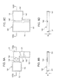
- the conductive frame member 130 shown in FIGS. 8A and 8B is adapted for the electromagnetic shield region 110 , FIG. 8A is a top view, and FIG. 8B is a sectional view taken along line VIIIB-VIIIB in FIG. 8A .
- the conductive frame member 130 includes a frame wall portion 131 which stands vertically on the surface of the printed wiring board 100 when provided on the printed wiring board 100 , and reinforcing bridging portions 132 , 133 , 134 , and 135 for reinforcing the frame wall portion 131 which surrounds the electromagnetic shield region 110 .
- the reinforcing bridging portions 132 , 133 , 134 , and 135 are formed by bridging separate positions of the frame member 131 using a metal thin plate on the upper end side opposite to the bonded portion between the frame wall portion 131 and the printed wiring board 100 .
- the height h 1 of the frame wall portion 131 of the conductive frame member 130 from the printed wiring board 100 is set to be equal to or slightly larger than the total of the height, from the printed wiring board 100 , of the highest one among the electronic components 101 , 102 , . . . in the electromagnetic shield region 110 , and the thickness of the reinforcing bridge portions 132 , 133 , 134 , and 135 .
- the height h 1 is such a height that when the conductive frame member 130 is covered with a plane in contact with the upper end of the frame wall portion 131 , the plane does not contact the electronic components 101 , 102 , . . . in the electromagnetic shield region 110 .
- the conductive frame member 140 shown in FIGS. 8C and 8D is adapted for the electromagnetic shield region 120
- FIG. 8C is a top view
- FIG. 8D is a sectional view taken along line VIIID-VIIID in FIG. 8C
- the conductive frame member 140 includes a frame wall portion 141 which stands vertically on the surface of the printed wiring board 100 when provided on the printed wiring board 100 , and a reinforcing bridging portion 142 for reinforcing the frame wall portion 141 which surrounds the electromagnetic shield region 111 .
- the reinforcing bridging portion 142 is formed by bridging separated positions of the frame wall portion 141 using a metal thin plate on the upper end side opposite to the bonded portion between the frame wall portion 141 and the printed Wiring board 100 .
- the height h 2 of the frame wall portion 141 of the conductive frame member 140 from the printed wiring board 100 is set to be equal to or slightly larger than the total of the height, from the printed wiring board 100 , of the highest one among the electronic components 103 , 104 , . . . in the electromagnetic shield region 120 , and the thickness of the reinforcing bridge portion 142 .
- the height h 2 is such a height that when the conductive frame member 140 is covered with a plane in contact with the upper end of the frame wall portion 141 , the plane does not contact the electronic components 103 , 104 , . . . in the electromagnetic shield region 120 .
- the fourth embodiment does not use a cover member made of a metal thin plate formed using a mold for each of the conductive frame members 130 and 140 . Instead, the same electromagnetic shielding film as in the above-described embodiments is used. The electromagnetic shielding film used in the fourth embodiment is described.
- FIGS. 9A and 9B show an electromagnetic shielding film 150 alternative to a cover member for the conductive frame member 130 for the electromagnetic shield region 110 , in which FIG. 9A is a plan view, and FIG. 9B is a sectional view taken along line IXB-IXB in FIG. 9A .
- FIGS. 10A and 10B show an electromagnetic shielding film 160 alternative to a cover member for the conductive frame member 140 for the electromagnetic shield region 120 , in which FIG. 10A is a plan view, and FIG. 10B is a sectional view taken along line XB-XB in FIG. 10A .
- the electromagnetic shielding film 150 is formed in a planar shape corresponding to the shape of the electromagnetic shield region 110 of the printed wiring board 100 .
- the electromagnetic shielding film 160 is formed in a planar shape corresponding to the shape of the electromagnetic shield region 120 of the printed wiring board 100 .
- each of the electromagnetic shielding films 150 and 160 is a laminate film including a conductive metal layer 151 or 161 and an insulating layer, in this example, an insulating resin layer 153 or 163 , which are laminated with a conductive adhesive layer 152 or 162 provided therebetween.
- the insulating resin layers 153 and 163 are not laminated to expose the conductive adhesive layers 152 and 162 in peripheral portions 150 e and 160 e of the electromagnetic shielding films 150 and 160 shown by dotted lines in FIGS. 9A and 10A , respectively.
- the width d of the peripheral portions 150 e and 160 e in which the conductive adhesive layers 152 and 162 are respectively exposed corresponds to or is slightly larger than the width of the upper end surfaces of the frame wall portions 131 and 141 of the conductive frame members 130 and 140 .
- the width d of the peripheral portions 150 e and 160 e in which the conductive adhesive layers 152 and 162 are respectively exposed may be smaller than the width of the upper end surfaces of the frame wall portions 131 and 141 of the conductive frame members 130 and 140 as long as the conductive frame members 130 and 140 are sufficiently bonded to the electromagnetic shielding films 150 and 160 on the upper end surfaces of the conductive frame members 130 and 140 , respectively.
- the conductive metal layers 151 and 161 are composed of, for example, an aluminum sheet.
- the conductive adhesive layers 152 and 162 are composed of an epoxy resin containing metal fine particles.
- the insulating resin layers 153 and 163 are composed of, for example, PET (Polyethylene Terephthalate Resin).
- the thickness of the electromagnetic shielding films 150 and 160 may be 30 ⁇ m to 100 ⁇ m. Since the thickness of the cover member made of a metal thin plate of a can shield is 0.2 mm, the thickness of the electromagnetic shielding films 150 and 160 according to this embodiment is 1 ⁇ 2 or less of the cover member made of the metal thin plate of the can shield.
- the conductive adhesive layers 152 and 162 are layers composed of an adhesive which is bondable at room temperature. Therefore, the electromagnetic shielding films 150 and 160 are provided in a state of being bonded to release paper with the conductive adhesive layers 152 and 162 , respectively. The electromagnetic shielding films 150 and 160 are used by peeling from the release paper.
- the conductive frame members 130 and 140 previously formed using molds as described above are mounted on the printed wiring board 100 so as to fit the shapes of the electromagnetic shield regions 110 and 120 , respectively, of the printed wiring board 100 .
- a mounting state is shown in FIGS. 11A and 11B .
- FIG. 11A is a top plan view of the printed wiring board 100 as viewed from the surface on which the electronic components 101 , 102 , 103 , 104 , . . . , such as IC and the like, are mounted.
- FIG. 11B is a sectional view taken along line XIB-XIB in FIG. 11A .
- a grounding conductor pattern is formed along each of the electromagnetic shield regions 110 and 120 on the printed wiring board 100 .
- the conductive frame members 130 and 140 are bonded and electrically grounded by soldering to the respective grounding conductor patterns of the printed wiring board 100 at the bonded end surfaces between the frame wall portions 131 and 141 and the printed wiring board 100 .
- the first step is completed.
- the electromagnetic shielding film 150 separated from the release paper is placed on the conductive frame member 130 so that the peripheral portion 150 e in which the conductive adhesive layer 152 is exposed contacts the upper end surface of the frame wall portion 131 of the conductive frame member 130 as shown in FIGS. 12A and 12B and further in an enlarged partial view of FIG. 12B .
- the peripheral portion 150 e of the electromagnetic shielding film 150 in which the conductive adhesive layer 152 is exposed in contact with the upper end surface of the frame wall portion 131 of the conductive frame member 130 is pressed on the upper end surface of the frame wall portion 131 of the conductive frame member 130 as shown by an arrow in FIG. 12B , thereby bonding the electromagnetic shielding film 150 to the upper end surface of the frame wall portion 131 of the conductive frame member 130 .
- the electromagnetic shielding film 150 is electrically connected to the conductive frame member 130 which is electrically connected to a grounding conductor of the printed wiring board 100 .
- the electromagnetic shield region 110 of the printed wiring board 100 is covered with the electromagnetic shielding film 150 and the conductive frame member 130 electrically connected to the grounding conductor of the printed wiring board 100 , thereby realizing an electromagnetic shield.
- the electromagnetic shielding film 160 separated from the release paper is placed on the conductive frame member 140 so that the peripheral portion 160 e in which the conductive adhesive layer 162 is exposed contacts the upper end surface of the frame wall portion 141 of the conductive frame member 140 as shown in FIGS. 12A and 12B and further in an enlarged partial view of FIG. 12B .
- the peripheral portion 160 e of the electromagnetic shielding film 160 in which the conductive adhesive layer 162 is exposed in contact with the upper end surface of the frame wall portion 141 of the conductive frame member 140 is pressed on the upper end surface of the frame wall portion 141 of the conductive frame member 140 , thereby bonding the electromagnetic shielding film 160 to the upper end surface of the frame wall portion 141 of the conductive frame member 140 .
- the electromagnetic shielding film 160 is electrically connected to the conductive frame member 140 which is electrically connected to a grounding conductor of the printed wiring board 100 .
- the electromagnetic shield region 120 of the printed wiring board 100 is covered with the electromagnetic shielding film 160 and the conductive frame member 140 electrically connected to the grounding conductor of the printed wiring board 100 , thereby realizing an electromagnetic shield.
- the insulating layers are laminated on the conductive adhesive layers 152 and 162 of the electromagnetic shielding films 150 and 160 , excluding the peripheral portions 150 e and 160 e , respectively. Even when conductors likely to be in contact with the electromagnetic shielding films 150 and 160 are present in the electromagnetic shield regions 110 and 120 of the printed wiring board 100 , insulation between the conductors and the conductive metal layers 151 and 161 of the electromagnetic shielding films 150 and 160 is secured by the insulating layers.
- each of the electromagnetic shielding films 150 and 160 may include two layers, not the three layers, as shown in FIGS. 13A and 13B .
- the electromagnetic shielding film 150 may include a laminate of the conductive metal layer 151 (or 161 ) and the conductive adhesive layer 152 (or 162 ).
- the conductive adhesive layer 152 may be laminated only on the peripheral portion of the conductive metal layer 151 (or 161 ).
- the electromagnetic shielding films 150 and 160 shown in FIGS. 13A and 13B are usually adhered to release paper with the conductive adhesive layers 152 and 162 , respectively, and are thus used after the release paper is separated.
- the width d of the peripheral portions 150 e and 160 e in which the conductive adhesive layers 152 and 162 of the electromagnetic shielding films 150 and 160 are respectively exposed may correspond to a width slightly larger than the width of the upper end surfaces of the frame wall portions 131 and 141 of the conductive frame members 130 and 140 .
- the shapes of the electromagnetic shielding films 150 and 160 may be slightly larger than the frame shapes of the conductive frame members 130 and 140 , not precisely coincide with the frame shapes of the conductive frame members 130 and 140 , respectively.
- the ends of the peripheral portions 150 e and 160 e in which the conductive adhesive layers 152 and 162 of the electromagnetic shielding films 150 and 160 are respectively exposed project outward from the frame wall portions 131 and 141 of the conductive frame members 130 and 140 , respectively.
- the end portions may be cut with a cutter or may be bonded to the outer side surfaces of the frame wall portions 131 and 141 of the conductive frame members 130 and 140 , respectively, as shown in FIG. 14 .
- the conductive frame members 130 and 140 are formed using molds, but the electromagnetic shielding films 150 and 160 are used in place of the cover members to be engaged with the conductive frame members 130 and 140 , respectively.
- the electromagnetic shielding films 150 and 160 are formed at low cost as compared with the cover members formed using molds.
- the cost is decreased as compared with the case of a can shield including a conductive frame member and a cover member formed using molds. Since the cost of forming the cover member made of a metal thin plate using a mold is usually higher than the cost of forming the conductive frame member using a mold, the cost in the fourth embodiment may be expected to be decreased to 1 ⁇ 2 or less of the cost of the can shield.
- the electromagnetic shielding films are bonded to the upper ends of the frame wall portions 131 and 141 of the conductive frame members 130 and 140 , respectively, not bonded directly to the respective grounding conductor pattern's of the printed wiring board 100 . Therefore, the electromagnetic shielding films are simply fixed to the printed wiring board 100 through the conductive frame members 130 and 140 without using a jig such as a thermocompression bonding bar or the like.
- electromagnetic shielding may be more securely and strongly performed than in the case in which the electromagnetic shielding films are bonded directly to the respective grounding conductor patterns of the printed wiring board 100 .
- the electromagnetic shielding films are easily separated from and again bonded to the respective electromagnetic shield regions of the printed wiring board 100 , thereby facilitating change of electronic components in the electromagnetic shield regions.
- the electromagnetic shielding film may be configured by the two layers including the conductive metal layer and the conductive adhesive layer without using the insulating resin layer, thereby realizing further thinning.
- the electromagnetic shielding films may be bonded to the respective conductive frame members at room temperature, thereby causing the effect of improving workability in comparison with the first to third embodiments.
- the shapes of the electromagnetic shielding films 150 and 160 may be slightly larger than the frame shapes of the conductive frame members 130 and 140 , respectively, not precisely agree with the frame shapes. There is thus the advantage that the shapes of the electromagnetic shielding films 150 and 160 may be roughly formed.
- the portions of the electromagnetic shielding films 150 and 160 which project from the frames of the conductive frame members 130 and 140 may be adhered to the outer side surfaces of the frame wall portions 131 and 141 of the conductive frame members 130 and 140 , respectively. There is thus the advantage of enhancing adhesion and bonding property between the electromagnetic shielding films 150 and 160 and the conductive frame members 130 and 140 , respectively.
- the electromagnetic shielding films 150 and 160 having shapes corresponding to the shapes of the electromagnetic shield regions 110 and 120 , respectively, of the printed wiring board 100 .
- the electromagnetic shielding film 10 shown in FIG. 1A of the first embodiment is used as an electromagnetic shielding film.
- the electromagnetic shielding methods according to the first and fourth embodiments are combined.
- the electromagnetic shielding method according to the fifth embodiment is described by taking, for example, the electromagnetic shielding for the printed wiring board 100 described in the fourth embodiment.
- the first step in the fifth embodiment is completely the same as in the fourth embodiment. Namely, conductive frame members 130 and 140 are disposed in electromagnetic shield regions 110 and 120 , respectively, of a printed wiring board 100 , and soldered to respective grounding conductor patterns.
- the second step and subsequent steps are different from those in the fourth embodiment.
- the electromagnetic shielding film 10 of the above-described first embodiment is disposed to cover each of the electromagnetic shield regions 110 and 120 of the printed wiring board 100 .
- the electromagnetic shielding film 10 is disposed so that the insulating resin layer 13 faces the printed wiring board 100 and the electromagnetic shielding film 10 projects outward from at least each of the frame wall portions 131 and 141 of the conductive frame members 130 and 140 .
- thermocompression bonding bar 40 heated to a predetermined temperature is pressed to the upper end surface of the frame wall portion 131 or 141 of the conductive frame member 130 or 140 on the printed wiring board 100 from the conductive metal layer 11 of the electromagnetic shielding film 10 by the same method as in the electromagnetic shielding method of the first embodiment described with reference to FIGS. 2A to 2C .
- the third step may be first performed for the conductive frame member 130 in the electromagnetic shield region 110 and then performed for the conductive frame member 140 .
- the third step may be simultaneously performed for both conductive frame members 130 and 140 .
- the heating temperature of the thermocompression bonding bar 40 is higher than the melting temperatures of the insulating resin layer 13 and the conductive adhesive layer 12 and lower than the melting temperature of the conductive metal layer 11 , for example, about 150° C. to 170° C.
- thermocompression bonding bar 40 is provided to an arm 51 of a moving device 50 .
- the thermocompression bonding bar 40 is automatically moved along the upper end surfaces of the frame wall portions 131 and 141 of the conductive frame members 130 and 140 on the basis of moving position setting information of an operator.
- the moving device 50 is configured to store arrangement information of the upper end surfaces of the frame wall portions 131 and 141 of the conductive frame members 130 and 140 on the printed wiring board 100 so that the information is displayed on a display screen provided in the moving device 50 .
- the operator determines a moving path of the thermocompression bonding bar 40 according to the arrangement information displayed on the display screen about the upper end surfaces of the frame wall portions 131 and 141 of the conductive frame members 130 and 140 .
- thermocompression bonding bar 40 moves to the starting point of the set moving path and downwardly moves the thermocompression bonding bar 40 so as to press the conductive metal layer 11 of the electromagnetic shielding film 10 to the upper end surface 131 a or 141 a ( 141 a not shown) of the frame wall portion 131 or 141 of the conductive frame member 130 or 140 .
- the temperature of the thermocompression bonding bar 40 is controlled to about 150° C. to 170° C. by the heating device 52 .
- the moving device 50 moves the thermocompression bonding bar 40 so as to trace the upper end surface 131 a or 141 a ( 141 a not shown) of the frame wall portion 131 or 141 of the conductive frame member 130 or 140 in a state in which the electromagnetic shielding film 10 is pressed to the upper end surface 131 a or 141 a ( 141 a not shown) of the frame wall portion 131 or 141 of the conductive frame member 130 or 140 .
- the insulating resin layer 13 is melted and contracted by heat in a portion of the electromagnetic shielding film 10 which is heated and pressed with the thermocompression bonding bar 40 . Therefore, in the portion of the electromagnetic shielding film 10 which is heated and pressed with the thermocompression bonding bar 40 , the insulating resin layer 13 is excluded by pressure of the thermocompression bonding bar 40 , and the melted conductive adhesive layer 12 is bonded to the upper end surface 131 a or 141 a ( 141 a not shown) of the frame wall portion 131 or 141 of the conductive frame member 130 or 140 . Consequently, the conductive metal layer 11 of the electromagnetic shielding film 10 is electrically connected to the conductive frame member 130 or 140 .
- the electromagnetic shielding film 10 is bonded to the conductive frame member 130 or 140 disposed on the printed wiring board 100 by trace-moving the thermocompression bonding bar 40 , and the conductive metal layer 11 of the electromagnetic shielding film 10 is electrically connected to the grounding conductor pattern of the printed wiring board 100 .
- electromagnetic shielding for the electromagnetic shield region 110 or 120 on the printed wiring board 100 is formed.
- a cutter 60 for cutting the electromagnetic shielding film 10 is attached to the arm 51 (refer to FIG. 3A ) of the moving device 50 in place of the thermocompression bonding bar 40 .
- the position of the arm 51 is finely controlled so that the edge of the cutter 60 is positioned outside a portion to be electromagnetically shielded, the portion being a bonded portion between the conductive metal layer 11 of the electromagnetic shielding film 10 and the frame wall portion 131 or 141 of the conductive frame member 130 or 140 .
- the operator instructs the moving device 50 to move the cutter 60 downward so that the edge thereof is positioned at a cutting position of the electromagnetic shielding film 10 and move the cutter 60 to trace the frame wall portion 131 or 141 of the conductive frame member 130 or 140 like in the case of the thermocompression bonding bar 40 .
- an excess portion of the electromagnetic shielding film 10 is cut off.
- electromagnetic shielding for the electromagnetic shield region of the printed wiring board 100 is completed.
- electromagnetic shielding may be realized using the electromagnetic shielding film 10 S having the configuration shown in FIG. 1B .
- the step (third step) of connecting the conductive metal layer 11 of the electromagnetic shielding film 10 to each of the conductive frame members and the step (fourth step) of removing an excess portion of the electromagnetic shielding film 10 are separated from each other.
- thermocompression bonding bar 70 with a cutter as shown in FIG. 4 in place of the thermocompression bonding bar 40 .
- the fourth step of cutting off an extra portion of the electromagnetic shielding film 10 may be omitted.
- thermocompression bonding bar 40 is moved to trace the upper end surface of the frame wall portion 131 or 141 of the conductive frame member 130 or 140 so that the electromagnetic shielding film 10 or 10 S is continuously bonded to the upper end surface of the frame wall portion 131 or 141 of the conductive frame member 130 or 140 with the conductive adhesive layer 12 of the electromagnetic shielding film 10 or 10 S.
- thermocompression bonding bar 40 is pressed on the electromagnetic shielding film 10 at separate positions on the upper end surface of the frame wall portion 131 or 141 of the conductive frame member 130 or 140 so that the conductive metal layer 11 of the electromagnetic shielding film 10 is bonded and electrically connected to the upper end surface of the frame wall portion 131 or 141 of the conductive frame member 130 or 140 at the separate positions.
- the electromagnetic shielding film 10 or 105 is bonded to the upper end surface of each of the frame wall portions 131 and 141 of the conductive frame members 130 and 140 .
- the electromagnetic shielding film 10 may be bonded to the peripheral side surface of each of the frame wall portions 131 and 141 . This case corresponds to the sixth embodiment.
- the first and second steps are completely the same as in the fifth embodiment.
- a state shown in FIG. 16A is produced by the same method as in the fifth embodiment shown in FIGS. 15A and 15B .
- thermocompression bonding bar 90 with a cutter is attached to the moving device 50 (refer to FIG. 4 ). Then, the electromagnetic shielding film 10 is cut with the cutter edge by pressing the thermocompression bonding bar 90 with a cutter against the peripheral side surface 131 s or 141 s ( 141 s not shown) of the frame wall portion 131 or 141 of the conductive frame member 130 or 140 under heating with the heating device 52 .
- the temperature of the thermocompression bonding bar 90 with a cutter is controlled to about 150° C. to 170° C. by the heating device 52 .
- the operator instructs the moving device 50 to start movement of the thermocompression bonding bar 90 with a cutter along the set moving path.
- the moving device 50 moves the thermocompression bonding bar 90 with a cutter along the peripheral side surface 131 s or 141 s ( 141 s not shown) of the frame wall portion 131 or 141 in a state in which the electromagnetic shielding film 10 is pressed to the peripheral side surface 131 s or 141 s ( 141 s not shown) of the frame wall portion 131 or 141 of the conductive frame member 130 or 140 .
- the insulating resin layer 13 is melted and contracted by heat in a portion of the electromagnetic shielding film 10 which is heated and pressed with the thermocompression bonding bar 90 with a cutter. Therefore, in the portion of the electromagnetic shielding film 10 which is heated and pressed with the thermocompression bonding bar 90 with a cutter, the insulating resin layer 13 is excluded by pressure of the thermocompression bonding bar 90 with a cutter, and the melted conductive adhesive layer 12 is bonded to the peripheral side surface 131 s or 141 s ( 141 s not shown) of the frame wall portion 131 or 141 of the conductive frame member 130 or 140 . Consequently, the conductive metal layer 11 of the electromagnetic shielding film 10 is electrically connected to the conductive frame member 130 or 140 .
- the electromagnetic shielding film 10 is bonded to the conductive frame member 130 or 140 mounted on the printed wiring board 100 by trace-moving the thermocompression bonding bar 90 with a cutter, and the conductive metal layer 11 of the electromagnetic shielding film 10 is electrically connected to the grounding conductor pattern of the printed wiring board 100 .
- electromagnetic shielding is formed for the electromagnetic shield region 110 or 120 of the printed wiring board 100 .
- the third step may be first performed for the conductive frame member 130 in the electromagnetic shield region 110 and then performed for the conductive frame member 140 .
- the third step may be simultaneously performed for both the conductive frame members 130 and 140 .
- the electromagnetic shielding film 10 is cut on the printed wiring board 100 .
- the edge of the cutter may be disposed in contact with the peripheral side surface of the frame wall portion 131 s or 141 s of the conductive frame member 130 or 140 so that the electromagnetic shielding film 10 is cut on the peripheral side surface of the frame wall portion 131 s or 141 s of the conductive frame member 130 or 140 .
- electromagnetic shielding film 10 having the configuration shown in FIG. 1A is described.
- electromagnetic shielding may be realized using the electromagnetic shielding film 10 having the configuration shown in FIG. 1B .
- the electromagnetic shielding film may be bonded to not only the peripheral side surface of the frame wall portion of the conductive frame member but also the upper end surface of the frame wall portion.
- the electromagnetic shielding films 150 and 160 are previously prepared to have shapes precisely coinciding with the shapes of the respective electromagnetic shield regions.
- the electromagnetic shielding films may be roughly formed by providing the cutting step of the fifth embodiment.
- the electromagnetic shielding films 150 and 160 may be formed to shapes slightly larger than the frame shapes of the conductive frame members 130 and 140 corresponding to the electromagnetic shield regions 110 and 120 , respectively.
- the electromagnetic shielding films 150 and 160 are bonded to the upper end surfaces of the frame wall portions 131 and 141 of the conductive frame members 130 and 140 , respectively, and then projecting portions of the electromagnetic shielding films 150 and 160 are cut with the cutter.
- two-layer electromagnetic shielding films each including the conductive metal layer and the conductive adhesive layer may be used.
- the electromagnetic shielding films 150 and 160 are formed to shapes slightly larger than the frame shapes of the conductive frame members 130 and 140 corresponding to the electromagnetic shield regions 110 and 120 , respectively. In this case, portions projecting from the upper end surfaces of the frame wall portions 131 and 141 of the conductive frame members 130 and 140 are adhered to the peripheral side surfaces of the frame wall portions 131 and 141 of the conductive frame members 130 and 140 .
- two-layer electromagnetic shielding films each including the conductive metal layer and the conductive adhesive layer may be used.
- thermocompression bonding step is not performed.
- the electromagnetic shielding films 150 and 160 are not precisely positioned on the conductive frame members 130 and 140 , respectively, thereby causing the effect of simplifying the work as compared with the fourth embodiment.
- each of the electromagnetic shielding films is bonded to the conductive frame member with the conductive adhesive layer exposed in at least the peripheral portion of the electromagnetic shielding film.
- grounding conductor patterns may be formed to surround the respective electromagnetic shield regions 110 and 120 so that the electromagnetic shielding films 150 and 160 are bonded to the respective grounding conductor patterns with the conductive adhesive layers in the peripheral portions.
- the insulating layer may be provided or not provided according to the conditions in the electromagnetic shield regions.
- the conductive frame members are made of a conductive metal
- the material is not limited to the conductive metal as long as the conductive frame members are composed of a conductive material.
Abstract
Description
Claims (1)
Priority Applications (1)
| Application Number | Priority Date | Filing Date | Title |
|---|---|---|---|
| US13/531,688 US8853562B2 (en) | 2009-05-22 | 2012-06-25 | Electromagnetic shielding method and electromagnetic shielding film |
Applications Claiming Priority (8)
| Application Number | Priority Date | Filing Date | Title |
|---|---|---|---|
| JP2009123715 | 2009-05-22 | ||
| JPP2009-123715 | 2009-05-22 | ||
| JPP2009-138978 | 2009-06-10 | ||
| JP2009138978 | 2009-06-10 | ||
| JP2009262700A JP2011018873A (en) | 2009-05-22 | 2009-11-18 | Electromagnetic shielding method and electromagnetic shielding film |
| JPP2009-262700 | 2009-11-18 | ||
| US12/780,030 US8495815B2 (en) | 2009-05-22 | 2010-05-14 | Electromagnetic shielding method and electromagnetic shielding film |
| US13/531,688 US8853562B2 (en) | 2009-05-22 | 2012-06-25 | Electromagnetic shielding method and electromagnetic shielding film |
Related Parent Applications (1)
| Application Number | Title | Priority Date | Filing Date |
|---|---|---|---|
| US12/780,030 Division US8495815B2 (en) | 2009-05-22 | 2010-05-14 | Electromagnetic shielding method and electromagnetic shielding film |
Publications (2)
| Publication Number | Publication Date |
|---|---|
| US20120261181A1 US20120261181A1 (en) | 2012-10-18 |
| US8853562B2 true US8853562B2 (en) | 2014-10-07 |
Family
ID=42676658
Family Applications (2)
| Application Number | Title | Priority Date | Filing Date |
|---|---|---|---|
| US12/780,030 Expired - Fee Related US8495815B2 (en) | 2009-05-22 | 2010-05-14 | Electromagnetic shielding method and electromagnetic shielding film |
| US13/531,688 Expired - Fee Related US8853562B2 (en) | 2009-05-22 | 2012-06-25 | Electromagnetic shielding method and electromagnetic shielding film |
Family Applications Before (1)
| Application Number | Title | Priority Date | Filing Date |
|---|---|---|---|
| US12/780,030 Expired - Fee Related US8495815B2 (en) | 2009-05-22 | 2010-05-14 | Electromagnetic shielding method and electromagnetic shielding film |
Country Status (4)
| Country | Link |
|---|---|
| US (2) | US8495815B2 (en) |
| EP (1) | EP2254401B1 (en) |
| JP (1) | JP2011018873A (en) |
| CN (1) | CN101896058B (en) |
Cited By (6)
| Publication number | Priority date | Publication date | Assignee | Title |
|---|---|---|---|---|
| US20160174403A1 (en) * | 2014-12-11 | 2016-06-16 | Shenzhen Futaihong Precision Industry Co., Ltd. | Housing, electronic device using same, and method for making same |
| US20190281734A1 (en) * | 2016-11-02 | 2019-09-12 | Amogreentech Co., Ltd. | Electromagnetic wave shielding sheet for shield-can |
| US10477738B2 (en) | 2017-03-06 | 2019-11-12 | Laird Technologies, Inc. | Board level shields and systems and methods of applying board level shielding |
| US10834858B2 (en) | 2018-02-01 | 2020-11-10 | Henkel IP & Holding GmbH | Method for shielding system-in-package assemblies from electromagnetic interference |
| US11056251B2 (en) * | 2018-11-02 | 2021-07-06 | Jin Young Global Co., Ltd. | Patterning formation method, manufacturing method of electrical devices using the same and vehicular electrical device |
| US11695195B2 (en) | 2016-06-21 | 2023-07-04 | 3M Innovative Properties Company | Self-supporting antenna |
Families Citing this family (41)
| Publication number | Priority date | Publication date | Assignee | Title |
|---|---|---|---|---|
| EP2469976B1 (en) * | 2009-08-20 | 2015-03-25 | Panasonic Corporation | Electromagnetic wave heating device |
| US8279625B2 (en) * | 2010-12-14 | 2012-10-02 | Apple Inc. | Printed circuit board radio-frequency shielding structures |
| TWI471086B (en) * | 2011-03-14 | 2015-01-21 | E Ink Holdings Inc | A method for forming an emi shielding layer on an electronic paper display |
| JP5743251B2 (en) * | 2011-05-06 | 2015-07-01 | ▲華▼▲為▼▲終▼端有限公司 | Composite materials and electronic devices |
| US9179538B2 (en) | 2011-06-09 | 2015-11-03 | Apple Inc. | Electromagnetic shielding structures for selectively shielding components on a substrate |
| CN102711428B (en) * | 2012-06-21 | 2015-11-18 | 广州方邦电子有限公司 | Ultra-thin shielding film of a kind of high screening effectiveness and preparation method thereof |
| US8969730B2 (en) * | 2012-08-16 | 2015-03-03 | Apple Inc. | Printed circuit solder connections |
| TW201409653A (en) * | 2012-08-24 | 2014-03-01 | Bridge Semiconductor Corp | Wiring board with embedded device and electromagnetic shielding |
| US9704613B2 (en) | 2013-02-21 | 2017-07-11 | 3M Innovative Properties Company | Polymer composites with electromagnetic interference mitigation properties |
| WO2014200035A1 (en) * | 2013-06-13 | 2014-12-18 | 住友ベークライト株式会社 | Electromagnetic wave shielding film, and electronic component mounting substrate |
| JP2017502513A (en) | 2013-12-18 | 2017-01-19 | スリーエム イノベイティブ プロパティズ カンパニー | Electromagnetic interference (EMI) shielding products using titanium monoxide (TIO) materials |
| CN103745771A (en) * | 2013-12-23 | 2014-04-23 | 杨天纬 | Wire used for signal transmission aspect |
| CN103763893B (en) * | 2014-01-14 | 2016-04-13 | 广州方邦电子股份有限公司 | Electromagnetic shielding film and comprise the manufacture method of wiring board of screened film |
| CN103747613A (en) * | 2014-01-15 | 2014-04-23 | 深圳市三惠科技有限公司 | Applicable electromagnetic wave protection film and manufacturing method thereof |
| CN105632686A (en) * | 2014-11-05 | 2016-06-01 | 武陟县电业总公司 | Fabrication method for shielding shell of transformer |
| WO2017019738A1 (en) * | 2015-07-30 | 2017-02-02 | Laird Technologies, Inc. | Soft and/or flexible emi shields and related methods |
| CN107241855B (en) * | 2015-08-24 | 2019-07-30 | 浙江展邦电子科技有限公司 | A kind of wiring board with shielding construction |
| CN105139922A (en) * | 2015-09-21 | 2015-12-09 | 杨天纬 | Shielding film used for cable, manufacturing method of shielding film, and manufacturing method of wire rod |
| CN105139923A (en) * | 2015-09-21 | 2015-12-09 | 杨天纬 | Shielding film used for cable, manufacturing method of shielding film, and manufacturing method of wire rod |
| US10652996B2 (en) * | 2015-12-21 | 2020-05-12 | 3M Innovative Properties Company | Formable shielding film |
| CN105611817A (en) * | 2015-12-23 | 2016-05-25 | 中国电子科技集团公司第三十三研究所 | Method for preparing electromagnetic protection flexible material |
| CN108601215B (en) * | 2016-02-25 | 2020-01-14 | Oppo广东移动通信有限公司 | Rigid-flex board and terminal |
| JP6623474B2 (en) * | 2016-03-28 | 2019-12-25 | 北川工業株式会社 | Heat conductive member, method for manufacturing heat conductive member, and heat conductive structure |
| DE102016206234A1 (en) * | 2016-04-14 | 2017-10-19 | Zf Friedrichshafen Ag | Power rail for an inverter, inverter and motor vehicle drive system |
| KR20170123747A (en) * | 2016-04-29 | 2017-11-09 | 삼성전자주식회사 | Shielding member and electronic device with the same |
| JP6846161B2 (en) * | 2016-10-28 | 2021-03-24 | 株式会社小糸製作所 | Manufacturing method of load drive device, vehicle lighting equipment and load drive device |
| KR102544367B1 (en) | 2016-11-08 | 2023-06-19 | 삼성전자주식회사 | Electronic device with electromagnetic shielding member |
| JP2018116983A (en) * | 2017-01-16 | 2018-07-26 | 富士通株式会社 | Electronic apparatus |
| US9901016B1 (en) * | 2017-04-14 | 2018-02-20 | Kinsus Interconnect Technology Corp. | Electromagnetic-interference shielding device |
| CN107148209A (en) * | 2017-06-30 | 2017-09-08 | 朱燕萍 | A kind of electromagnetic shielding film |
| US11197399B2 (en) * | 2018-02-28 | 2021-12-07 | Lifeline IP Holdings, LLC | Electromagnetic pulse shield |
| CN108377609B (en) * | 2018-04-25 | 2020-02-21 | 维沃移动通信有限公司 | Shielding film, flexible circuit board assembly and mobile terminal |
| JP7100559B2 (en) * | 2018-10-25 | 2022-07-13 | 株式会社ジャパンディスプレイ | Display device |
| KR102567412B1 (en) | 2018-10-31 | 2023-08-16 | 삼성전자주식회사 | Shield-film including a plurality of layers and electric device using the same |
| US10985109B2 (en) | 2018-12-27 | 2021-04-20 | STATS ChipPAC Pte. Ltd. | Shielded semiconductor packages with open terminals and methods of making via two-step process |
| TWI718540B (en) * | 2019-05-23 | 2021-02-11 | 元太科技工業股份有限公司 | Touch structure and manufacturing method thereof and touch display device |
| US11369051B2 (en) * | 2019-07-26 | 2022-06-21 | Samsung Electronics Co., Ltd. | Electromagnetic interference (EMI) shielding member and electronic device including the same |
| CN110842365A (en) * | 2019-11-26 | 2020-02-28 | 佳普电子新材料(连云港)有限公司 | Laser surface treatment process for metal base material of shielding material |
| CN111343782B (en) * | 2020-04-14 | 2021-04-27 | 京东方科技集团股份有限公司 | Flexible circuit board assembly, display assembly and display device |
| CN111710238A (en) * | 2020-07-22 | 2020-09-25 | 京东方科技集团股份有限公司 | Display device and electronic apparatus |
| CN114539584A (en) * | 2022-02-28 | 2022-05-27 | 广东派尔新材料科技有限公司 | Insulating coating of high-insulating-property electromagnetic shielding film and preparation method thereof |
Citations (67)
| Publication number | Priority date | Publication date | Assignee | Title |
|---|---|---|---|---|
| US3457070A (en) * | 1964-07-25 | 1969-07-22 | Matsuragawa Electric Co Ltd | Electrophotography |
| US3693251A (en) * | 1970-12-03 | 1972-09-26 | Bell Telephone Labor Inc | Method of forming closely spaced conductive layers |
| US4080085A (en) * | 1976-02-04 | 1978-03-21 | Minnesota Mining And Manufacturing Company | Traffic lane delineator system |
| US4517044A (en) * | 1981-11-18 | 1985-05-14 | Advanced Graphic Technology | Dry transfer decal and method of manufacture |
| US4708149A (en) * | 1985-06-14 | 1987-11-24 | Jens Axelgaard | Electrical stimulation electrode |
| US4865039A (en) * | 1985-08-21 | 1989-09-12 | Spring Creek Institute | Dry electrode system for detection of biopotentials and dry electrode for making electrical and mechanical connection to a living body |
| US4870969A (en) * | 1988-09-16 | 1989-10-03 | Somatics, Inc. | Electrode application system and method for electroconvulsive therapy |
| US4956031A (en) * | 1988-03-05 | 1990-09-11 | Stanley Electric Co., Ltd. | Method of manufacturing an elongated electroluminescence element |
| US4965408A (en) * | 1989-02-01 | 1990-10-23 | Borden, Inc. | Composite sheet material for electromagnetic radiation shielding |
| US5084124A (en) * | 1989-04-28 | 1992-01-28 | Nikkan Industries Co., Ltd. | Flexible printed circuit board and coverlay film and method of manufacturing same |
| US5153384A (en) * | 1989-08-26 | 1992-10-06 | Shinko Electric Industries, Co., Ltd. | Circuit board and process for manufacturing same |
| US5241137A (en) * | 1989-06-30 | 1993-08-31 | Sharp Kabushiki Kaisha | Flexible circuit board with an electrically insulating adhesive layer |
| JPH05304387A (en) | 1992-03-05 | 1993-11-16 | Nec Corp | Flexible shielding sheet |
| JPH06289513A (en) | 1993-03-30 | 1994-10-18 | Konica Corp | Method for dissolving photographic gelatinized matter |
| US5491301A (en) * | 1992-12-28 | 1996-02-13 | Hitachi, Ltd. | Shielding method and circuit board employing the same |
| US5554825A (en) * | 1994-11-14 | 1996-09-10 | The Whitaker Corporation | Flexible cable with a shield and a ground conductor |
| US5603158A (en) * | 1993-09-03 | 1997-02-18 | Nippon Graphite Industries Ltd. | Method for producing flexible circuit boards |
| EP0806891A1 (en) | 1996-05-08 | 1997-11-12 | W.L. GORE & ASSOCIATES, INC. | A lid assembly for shielding electronic components from EMI/RFI interferences |
| JPH1138172A (en) | 1997-07-14 | 1999-02-12 | Toshiba Corp | Offshore nuclear power plant, method for construction thereof, method for periodic inspection thereof, and offshore plant |
| WO1999057952A1 (en) | 1998-05-01 | 1999-11-11 | Minnesota Mining And Manufacturing Company | Emi shielding enclosures |
| US6238515B1 (en) * | 1998-08-18 | 2001-05-29 | Lintec Corporation | Wafer transfer apparatus |
| US20010025888A1 (en) * | 2000-02-29 | 2001-10-04 | Wataru Kakinoki | Information card and card shaped casing therefor |
| US6333466B1 (en) * | 1998-11-18 | 2001-12-25 | Nitto Denko Corporation | Flexible wiring board |
| US6353188B1 (en) * | 1997-02-05 | 2002-03-05 | Lear Corporation | Printed circuit assembly with flexible support |
| US20020029857A1 (en) * | 1999-08-09 | 2002-03-14 | Yukio Yamada | Process for mounting semiconductor device and mounting apparatus |
| US6399903B1 (en) * | 1999-03-01 | 2002-06-04 | Honeywell International Inc. | Multifunctional laminate structure and process |
| US6456000B1 (en) * | 1999-03-19 | 2002-09-24 | Samsung Sdi Co., Ltd. | Cathode ray tube with ITO layer and conductive ground strip |
| US20020189847A1 (en) * | 2000-07-12 | 2002-12-19 | Ryo Sakurai | Shielded flat cable |
| US20030006069A1 (en) * | 2001-06-19 | 2003-01-09 | Toru Takebe | Conductive bond, multilayer printed circuit board, and method for making the multilayer printed circuit board |
| WO2003015487A1 (en) | 2001-08-11 | 2003-02-20 | Ubinetics Limited | A method of providing radio frequency screening for electric components |
| US6620513B2 (en) * | 2000-07-03 | 2003-09-16 | Shin-Etsu Chemical Co., Ltd. | Base sheet for flexible printed circuit board |
| US20030180512A1 (en) * | 1998-05-14 | 2003-09-25 | Matsushita Electric Industrial Co., Ltd. | Circuit board and method of manufacturing the same |
| US20040041497A1 (en) * | 2002-06-12 | 2004-03-04 | Kazuaki Hamada | Piezoelectric sounding body and piezoelectric electroacoustic transducer using the same |
| US20040105223A1 (en) * | 2001-03-19 | 2004-06-03 | Ryoichi Okada | Method of manufacturing electronic part and electronic part obtained by the method |
| US6768654B2 (en) * | 2000-09-18 | 2004-07-27 | Wavezero, Inc. | Multi-layered structures and methods for manufacturing the multi-layered structures |
| US6768052B2 (en) * | 2002-02-08 | 2004-07-27 | Mitsumi Electric Co., Ltd. | Flexible printed circuit with EMI protection |
| US20040168824A1 (en) * | 2003-02-28 | 2004-09-02 | Olympus Corporation | Circuit board having deformation interrupting section and circuit board forming method |
| US6787915B2 (en) * | 2001-03-05 | 2004-09-07 | Oki Electric Industry Co., Ltd. | Rearrangement sheet, semiconductor device and method of manufacturing thereof |
| US6803528B1 (en) * | 1999-11-05 | 2004-10-12 | 3M Innovative Properties Company | Multi-layer double-sided wiring board and method of fabricating the same |
| US6825249B1 (en) * | 1994-12-26 | 2004-11-30 | Hitachi Chemical Co., Ltd. | Laminating method of film-shaped organic die-bonding material, die-bonding method, laminating machine and die-bonding apparatus, semiconductor device, and fabrication process of semiconductor device |
| US20040267188A1 (en) * | 2001-10-12 | 2004-12-30 | Francine Behar | Device for delivering medicines by transpalpebral electrophoresis |
| US6909615B2 (en) * | 2002-09-17 | 2005-06-21 | Wavezero, Inc. | Equipment and methods for producing continuous metallized thermoformable EMI shielding material |
| US20050150595A1 (en) * | 2003-12-10 | 2005-07-14 | Nitto Denko Corporation | Process for producing substrate for flexible circuit board |
| US6943288B1 (en) * | 2004-06-04 | 2005-09-13 | Schlegel Systems, Inc. | EMI foil laminate gasket |
| US20050211464A1 (en) * | 2003-01-08 | 2005-09-29 | Byun Jeong I | Method of microelectrode connection and connected structure of use threof |
| US20050248909A1 (en) * | 2002-08-01 | 2005-11-10 | Hideo Kikuchi | Electronic device including chip parts and a method for manufacturing the same |
| US20050276934A1 (en) * | 2002-11-29 | 2005-12-15 | Hiroji Fukui | Thermally vanishing material, transfer sheet using the same, and method for forming pattern |
| US20060084254A1 (en) * | 2004-01-06 | 2006-04-20 | Attarwala Abbas I | Method for making electronic packages |
| US20060152913A1 (en) | 2002-08-14 | 2006-07-13 | Manuel Richey | Method and apparatus for reducing electromagnetic emissions from electronic circuits |
| US20070013067A1 (en) * | 1999-01-29 | 2007-01-18 | Kazuto Nishida | Electronic component mounting method and apparatus |
| US20070046481A1 (en) * | 2005-09-01 | 2007-03-01 | Vokey David E | Moisture detection sensor tape with leak locate |
| US20070113961A1 (en) * | 2005-11-24 | 2007-05-24 | Nitto Denko Corporation | Conductor-clad laminate, wiring circuit board, and processes for producing the same |
| US20070120231A1 (en) * | 2004-06-30 | 2007-05-31 | Sony Chemical & Information Device Corporation | Transmission cable and method for manufacturing the same |
| US20070264496A1 (en) | 2006-05-12 | 2007-11-15 | Wavezero, Inc. | Solderable Plastic EMI Shielding |
| US7312400B2 (en) * | 2002-02-22 | 2007-12-25 | Fujikura Ltd. | Multilayer wiring board, base for multilayer wiring board, printed wiring board and its manufacturing method |
| US20080137020A1 (en) * | 2006-12-08 | 2008-06-12 | Epson Imaging Devices Corporation | Liquid crystal apparatus and electronic apparatus |
| US20080176359A1 (en) | 2007-01-18 | 2008-07-24 | Nokia Corporation | Method For Manufacturing Of Electronics Package |
| US20080298023A1 (en) * | 2007-05-28 | 2008-12-04 | Matsushita Electric Industrial Co., Ltd. | Electronic component-containing module and manufacturing method thereof |
| US20090145632A1 (en) * | 2005-10-25 | 2009-06-11 | Byd Company Limited | Flexible printed circuit and method for manufacturing the same |
| US20090236138A1 (en) * | 2008-03-13 | 2009-09-24 | Hiroshi Katagiri | Multilayer wiring board and method of manufacturing the same |
| US20090289341A1 (en) * | 2008-05-23 | 2009-11-26 | Semiconductor Energy Laboratory Co., Ltd. | Semiconductor device |
| US20100067235A1 (en) * | 2003-11-28 | 2010-03-18 | Semiconductor Energy Laboratory Co., Ltd. | Method of manufacturing display device |
| US20100248428A1 (en) * | 2009-03-27 | 2010-09-30 | Nitto Denko Corporation | Manufacturing method for semiconductor device |
| US20110091739A1 (en) * | 2008-06-24 | 2011-04-21 | Chikahito Sugahara | Composite material for electrical/electronic part and electrical/electronic part using the same |
| US20110308841A1 (en) * | 2009-03-06 | 2011-12-22 | Toshiyuki Kawaguchi | Coverlay film, method for manufacturing coverlay film, and flexible printed wiring board |
| US20120048603A1 (en) * | 2010-08-30 | 2012-03-01 | Foxconn Advanced Technology Inc. | Printed circuit board and method for manufacturing same |
| US8300194B2 (en) * | 2007-12-04 | 2012-10-30 | Chimei Innolux Corporation | Liquid crystal display having composite tape for preventing electrostatic discharge damage |
Family Cites Families (1)
| Publication number | Priority date | Publication date | Assignee | Title |
|---|---|---|---|---|
| DE102005001148B3 (en) * | 2005-01-10 | 2006-05-18 | Siemens Ag | Electronic unit, has metal housing coupled to MOSFET operated with high frequency, where housing is arranged to metal plate over electrically-isolated isolation layer, and heat sink electrically connected with metal plate or housing |
-
2009
- 2009-11-18 JP JP2009262700A patent/JP2011018873A/en not_active Withdrawn
-
2010
- 2010-05-14 US US12/780,030 patent/US8495815B2/en not_active Expired - Fee Related
- 2010-05-17 EP EP20100163014 patent/EP2254401B1/en not_active Not-in-force
- 2010-05-17 CN CN 201010181549 patent/CN101896058B/en not_active Expired - Fee Related
-
2012
- 2012-06-25 US US13/531,688 patent/US8853562B2/en not_active Expired - Fee Related
Patent Citations (72)
| Publication number | Priority date | Publication date | Assignee | Title |
|---|---|---|---|---|
| US3457070A (en) * | 1964-07-25 | 1969-07-22 | Matsuragawa Electric Co Ltd | Electrophotography |
| US3693251A (en) * | 1970-12-03 | 1972-09-26 | Bell Telephone Labor Inc | Method of forming closely spaced conductive layers |
| US4080085A (en) * | 1976-02-04 | 1978-03-21 | Minnesota Mining And Manufacturing Company | Traffic lane delineator system |
| US4517044A (en) * | 1981-11-18 | 1985-05-14 | Advanced Graphic Technology | Dry transfer decal and method of manufacture |
| US4708149A (en) * | 1985-06-14 | 1987-11-24 | Jens Axelgaard | Electrical stimulation electrode |
| US4865039A (en) * | 1985-08-21 | 1989-09-12 | Spring Creek Institute | Dry electrode system for detection of biopotentials and dry electrode for making electrical and mechanical connection to a living body |
| US4956031A (en) * | 1988-03-05 | 1990-09-11 | Stanley Electric Co., Ltd. | Method of manufacturing an elongated electroluminescence element |
| US4870969A (en) * | 1988-09-16 | 1989-10-03 | Somatics, Inc. | Electrode application system and method for electroconvulsive therapy |
| US4965408A (en) * | 1989-02-01 | 1990-10-23 | Borden, Inc. | Composite sheet material for electromagnetic radiation shielding |
| US5084124A (en) * | 1989-04-28 | 1992-01-28 | Nikkan Industries Co., Ltd. | Flexible printed circuit board and coverlay film and method of manufacturing same |
| US5241137A (en) * | 1989-06-30 | 1993-08-31 | Sharp Kabushiki Kaisha | Flexible circuit board with an electrically insulating adhesive layer |
| US5153384A (en) * | 1989-08-26 | 1992-10-06 | Shinko Electric Industries, Co., Ltd. | Circuit board and process for manufacturing same |
| JPH05304387A (en) | 1992-03-05 | 1993-11-16 | Nec Corp | Flexible shielding sheet |
| US5491301A (en) * | 1992-12-28 | 1996-02-13 | Hitachi, Ltd. | Shielding method and circuit board employing the same |
| JPH06289513A (en) | 1993-03-30 | 1994-10-18 | Konica Corp | Method for dissolving photographic gelatinized matter |
| US5603158A (en) * | 1993-09-03 | 1997-02-18 | Nippon Graphite Industries Ltd. | Method for producing flexible circuit boards |
| US5554825A (en) * | 1994-11-14 | 1996-09-10 | The Whitaker Corporation | Flexible cable with a shield and a ground conductor |
| US6825249B1 (en) * | 1994-12-26 | 2004-11-30 | Hitachi Chemical Co., Ltd. | Laminating method of film-shaped organic die-bonding material, die-bonding method, laminating machine and die-bonding apparatus, semiconductor device, and fabrication process of semiconductor device |
| EP0806891A1 (en) | 1996-05-08 | 1997-11-12 | W.L. GORE & ASSOCIATES, INC. | A lid assembly for shielding electronic components from EMI/RFI interferences |
| US6353188B1 (en) * | 1997-02-05 | 2002-03-05 | Lear Corporation | Printed circuit assembly with flexible support |
| JPH1138172A (en) | 1997-07-14 | 1999-02-12 | Toshiba Corp | Offshore nuclear power plant, method for construction thereof, method for periodic inspection thereof, and offshore plant |
| WO1999057952A1 (en) | 1998-05-01 | 1999-11-11 | Minnesota Mining And Manufacturing Company | Emi shielding enclosures |
| US20030180512A1 (en) * | 1998-05-14 | 2003-09-25 | Matsushita Electric Industrial Co., Ltd. | Circuit board and method of manufacturing the same |
| US6238515B1 (en) * | 1998-08-18 | 2001-05-29 | Lintec Corporation | Wafer transfer apparatus |
| US6333466B1 (en) * | 1998-11-18 | 2001-12-25 | Nitto Denko Corporation | Flexible wiring board |
| US20070013067A1 (en) * | 1999-01-29 | 2007-01-18 | Kazuto Nishida | Electronic component mounting method and apparatus |
| US6399903B1 (en) * | 1999-03-01 | 2002-06-04 | Honeywell International Inc. | Multifunctional laminate structure and process |
| US6456000B1 (en) * | 1999-03-19 | 2002-09-24 | Samsung Sdi Co., Ltd. | Cathode ray tube with ITO layer and conductive ground strip |
| US20020029857A1 (en) * | 1999-08-09 | 2002-03-14 | Yukio Yamada | Process for mounting semiconductor device and mounting apparatus |
| US6803528B1 (en) * | 1999-11-05 | 2004-10-12 | 3M Innovative Properties Company | Multi-layer double-sided wiring board and method of fabricating the same |
| US20010025888A1 (en) * | 2000-02-29 | 2001-10-04 | Wataru Kakinoki | Information card and card shaped casing therefor |
| US6620513B2 (en) * | 2000-07-03 | 2003-09-16 | Shin-Etsu Chemical Co., Ltd. | Base sheet for flexible printed circuit board |
| US6770820B2 (en) * | 2000-07-12 | 2004-08-03 | Kabushiki Kaisha Bridgestone | Shielded flat cable |
| US20020189847A1 (en) * | 2000-07-12 | 2002-12-19 | Ryo Sakurai | Shielded flat cable |
| US6768654B2 (en) * | 2000-09-18 | 2004-07-27 | Wavezero, Inc. | Multi-layered structures and methods for manufacturing the multi-layered structures |
| US6787915B2 (en) * | 2001-03-05 | 2004-09-07 | Oki Electric Industry Co., Ltd. | Rearrangement sheet, semiconductor device and method of manufacturing thereof |
| US20040105223A1 (en) * | 2001-03-19 | 2004-06-03 | Ryoichi Okada | Method of manufacturing electronic part and electronic part obtained by the method |
| US20030006069A1 (en) * | 2001-06-19 | 2003-01-09 | Toru Takebe | Conductive bond, multilayer printed circuit board, and method for making the multilayer printed circuit board |
| WO2003015487A1 (en) | 2001-08-11 | 2003-02-20 | Ubinetics Limited | A method of providing radio frequency screening for electric components |
| US20040267188A1 (en) * | 2001-10-12 | 2004-12-30 | Francine Behar | Device for delivering medicines by transpalpebral electrophoresis |
| US6768052B2 (en) * | 2002-02-08 | 2004-07-27 | Mitsumi Electric Co., Ltd. | Flexible printed circuit with EMI protection |
| US7312400B2 (en) * | 2002-02-22 | 2007-12-25 | Fujikura Ltd. | Multilayer wiring board, base for multilayer wiring board, printed wiring board and its manufacturing method |
| US20040041497A1 (en) * | 2002-06-12 | 2004-03-04 | Kazuaki Hamada | Piezoelectric sounding body and piezoelectric electroacoustic transducer using the same |
| US20050248909A1 (en) * | 2002-08-01 | 2005-11-10 | Hideo Kikuchi | Electronic device including chip parts and a method for manufacturing the same |
| US20060152913A1 (en) | 2002-08-14 | 2006-07-13 | Manuel Richey | Method and apparatus for reducing electromagnetic emissions from electronic circuits |
| US6909615B2 (en) * | 2002-09-17 | 2005-06-21 | Wavezero, Inc. | Equipment and methods for producing continuous metallized thermoformable EMI shielding material |
| US20050276934A1 (en) * | 2002-11-29 | 2005-12-15 | Hiroji Fukui | Thermally vanishing material, transfer sheet using the same, and method for forming pattern |
| US20050211464A1 (en) * | 2003-01-08 | 2005-09-29 | Byun Jeong I | Method of microelectrode connection and connected structure of use threof |
| US20070095563A1 (en) * | 2003-02-28 | 2007-05-03 | Olympus Corporation | Circuit board having deformation interrupting section and circuit board forming method |
| US20040168824A1 (en) * | 2003-02-28 | 2004-09-02 | Olympus Corporation | Circuit board having deformation interrupting section and circuit board forming method |
| US7935969B2 (en) * | 2003-11-28 | 2011-05-03 | Semiconductor Energy Laboratory Co., Ltd. | Method of manufacturing display device |
| US20100067235A1 (en) * | 2003-11-28 | 2010-03-18 | Semiconductor Energy Laboratory Co., Ltd. | Method of manufacturing display device |
| US20050150595A1 (en) * | 2003-12-10 | 2005-07-14 | Nitto Denko Corporation | Process for producing substrate for flexible circuit board |
| US20060084254A1 (en) * | 2004-01-06 | 2006-04-20 | Attarwala Abbas I | Method for making electronic packages |
| US6943288B1 (en) * | 2004-06-04 | 2005-09-13 | Schlegel Systems, Inc. | EMI foil laminate gasket |
| US20070120231A1 (en) * | 2004-06-30 | 2007-05-31 | Sony Chemical & Information Device Corporation | Transmission cable and method for manufacturing the same |
| US20080230254A1 (en) * | 2004-06-30 | 2008-09-25 | Sony Chemical & Information Device Corporation | Transmission cable |
| US20070046481A1 (en) * | 2005-09-01 | 2007-03-01 | Vokey David E | Moisture detection sensor tape with leak locate |
| US20090145632A1 (en) * | 2005-10-25 | 2009-06-11 | Byd Company Limited | Flexible printed circuit and method for manufacturing the same |
| US20070113961A1 (en) * | 2005-11-24 | 2007-05-24 | Nitto Denko Corporation | Conductor-clad laminate, wiring circuit board, and processes for producing the same |
| US20070264496A1 (en) | 2006-05-12 | 2007-11-15 | Wavezero, Inc. | Solderable Plastic EMI Shielding |
| US20080137020A1 (en) * | 2006-12-08 | 2008-06-12 | Epson Imaging Devices Corporation | Liquid crystal apparatus and electronic apparatus |
| US20080176359A1 (en) | 2007-01-18 | 2008-07-24 | Nokia Corporation | Method For Manufacturing Of Electronics Package |
| US20080298023A1 (en) * | 2007-05-28 | 2008-12-04 | Matsushita Electric Industrial Co., Ltd. | Electronic component-containing module and manufacturing method thereof |
| US8300194B2 (en) * | 2007-12-04 | 2012-10-30 | Chimei Innolux Corporation | Liquid crystal display having composite tape for preventing electrostatic discharge damage |
| US20090236138A1 (en) * | 2008-03-13 | 2009-09-24 | Hiroshi Katagiri | Multilayer wiring board and method of manufacturing the same |
| US8153909B2 (en) * | 2008-03-13 | 2012-04-10 | Ngk Spark Plug Co., Ltd. | Multilayer wiring board and method of manufacturing the same |
| US20090289341A1 (en) * | 2008-05-23 | 2009-11-26 | Semiconductor Energy Laboratory Co., Ltd. | Semiconductor device |
| US20110091739A1 (en) * | 2008-06-24 | 2011-04-21 | Chikahito Sugahara | Composite material for electrical/electronic part and electrical/electronic part using the same |
| US20110308841A1 (en) * | 2009-03-06 | 2011-12-22 | Toshiyuki Kawaguchi | Coverlay film, method for manufacturing coverlay film, and flexible printed wiring board |
| US20100248428A1 (en) * | 2009-03-27 | 2010-09-30 | Nitto Denko Corporation | Manufacturing method for semiconductor device |
| US20120048603A1 (en) * | 2010-08-30 | 2012-03-01 | Foxconn Advanced Technology Inc. | Printed circuit board and method for manufacturing same |
Cited By (9)
| Publication number | Priority date | Publication date | Assignee | Title |
|---|---|---|---|---|
| US20160174403A1 (en) * | 2014-12-11 | 2016-06-16 | Shenzhen Futaihong Precision Industry Co., Ltd. | Housing, electronic device using same, and method for making same |
| US9788431B2 (en) * | 2014-12-11 | 2017-10-10 | Shenzhen Futaihong Precision Industry Co., Ltd. | Housing, electronic device using same, and method for making same |
| US11695195B2 (en) | 2016-06-21 | 2023-07-04 | 3M Innovative Properties Company | Self-supporting antenna |
| US20190281734A1 (en) * | 2016-11-02 | 2019-09-12 | Amogreentech Co., Ltd. | Electromagnetic wave shielding sheet for shield-can |
| US10653047B2 (en) * | 2016-11-02 | 2020-05-12 | Amogreentech Co., Ltd. | Electromagnetic wave shielding sheet for shield-can |
| US10477738B2 (en) | 2017-03-06 | 2019-11-12 | Laird Technologies, Inc. | Board level shields and systems and methods of applying board level shielding |
| US10834858B2 (en) | 2018-02-01 | 2020-11-10 | Henkel IP & Holding GmbH | Method for shielding system-in-package assemblies from electromagnetic interference |
| US11304346B2 (en) | 2018-02-01 | 2022-04-12 | Henkel Ag & Co. Kgaa | Method for shielding system-in-package assemblies from electromagnetic interference |
| US11056251B2 (en) * | 2018-11-02 | 2021-07-06 | Jin Young Global Co., Ltd. | Patterning formation method, manufacturing method of electrical devices using the same and vehicular electrical device |
Also Published As
| Publication number | Publication date |
|---|---|
| CN101896058B (en) | 2012-11-28 |
| EP2254401A3 (en) | 2012-01-18 |
| EP2254401A2 (en) | 2010-11-24 |
| US20100294559A1 (en) | 2010-11-25 |
| JP2011018873A (en) | 2011-01-27 |
| CN101896058A (en) | 2010-11-24 |
| EP2254401B1 (en) | 2013-07-10 |
| US8495815B2 (en) | 2013-07-30 |
| US20120261181A1 (en) | 2012-10-18 |
Similar Documents
| Publication | Publication Date | Title |
|---|---|---|
| US8853562B2 (en) | Electromagnetic shielding method and electromagnetic shielding film | |
| CN207135434U (en) | Device, metallic shield and screened circuit including radome | |
| US9769920B2 (en) | Flexible printed circuits with bend retention structures | |
| TWI398201B (en) | Method of replacing unit wiring board of aggregate board, and aggregate board | |
| US20130130493A1 (en) | Connecting pad producing method | |
| JP2016058509A (en) | Method of manufacturing flexible printed wiring board with reinforcing plate and flexible printed wiring board intermediate | |
| JP2015176984A (en) | Printed wiring board | |
| CN212752722U (en) | Battery protection board and mobile terminal | |
| JP2014175423A (en) | Flexible substrate and mounting method thereof | |
| KR101576621B1 (en) | Antenna and method for manufacturing thereof | |
| JP6798472B2 (en) | Electronic devices and their manufacturing methods | |
| TW200841795A (en) | Flexible printed circuit, manufacture method of same and electronic device with same | |
| KR101460709B1 (en) | Laminated and integrated tape for taping the FPCB | |
| KR101363075B1 (en) | The method of manufacturing rigid-flexible printed circuit board | |
| JP5945801B2 (en) | Flexible printed wiring board and method for manufacturing flexible printed wiring board | |
| JP2003209390A (en) | Circuit board having electromagnetic shield, method for forming electromagnetic shield for circuit board, and forming equipment thereof | |
| WO2019174748A1 (en) | Assembly for electro-magnetic interference shielding and method | |
| CN107037924A (en) | The manufacturing process of circuit board module, sense of touch module and sense of touch module | |
| CN105956562B (en) | Slide fingerprint identifier and its manufacturing method | |
| CN112397669B (en) | Display module, manufacturing method thereof and display device | |
| CN214315745U (en) | Integrated flexible printed circuit board | |
| CN108401410B (en) | Printed circuit board suitable for top shielding case and lower shield cover | |
| JP5701712B2 (en) | RFID antenna sheet, RFID inlet, non-contact IC card, and non-contact IC tag | |
| TWI364872B (en) | ||
| KR102029722B1 (en) | Display device and method for the same |
Legal Events
| Date | Code | Title | Description |
|---|---|---|---|
| AS | Assignment |
Owner name: SONY ERICSSON MOBILE COMMUNICATIONS JAPAN, INC., J Free format text: ASSIGNMENT OF ASSIGNORS INTEREST;ASSIGNORS:IZAWA, KOICHI;OGURA, YUMI;REEL/FRAME:037893/0331 Effective date: 20100604 |
|
| AS | Assignment |
Owner name: SONY MOBILE COMMUNICATIONS JAPAN, INC., JAPAN Free format text: CHANGE OF NAME;ASSIGNOR:SONY ERICSSON MOBILE COMMUNICATIONS JAPAN, INC.;REEL/FRAME:038413/0811 Effective date: 20120308 Owner name: SONY MOBILE COMMUNICATIONS INC., JAPAN Free format text: CHANGE OF NAME;ASSIGNOR:SONY MOBILE COMMUNICATIONS JAPAN, INC.;REEL/FRAME:038413/0898 Effective date: 20130107 |
|
| AS | Assignment |
Owner name: SONY CORPORATION, JAPAN Free format text: ASSIGNMENT OF ASSIGNORS INTEREST;ASSIGNOR:SONY MOBILE COMMUNICATIONS INC.;REEL/FRAME:038380/0555 Effective date: 20130717 |
|
| AS | Assignment |
Owner name: SNAPTRACK, INC., CALIFORNIA Free format text: ASSIGNMENT OF ASSIGNORS INTEREST;ASSIGNORS:SONY CORPORATION;SONY MOBILE COMMUNICATIONS INC.;REEL/FRAME:039425/0093 Effective date: 20160729 |
|
| FEPP | Fee payment procedure |
Free format text: MAINTENANCE FEE REMINDER MAILED (ORIGINAL EVENT CODE: REM.) |
|
| LAPS | Lapse for failure to pay maintenance fees |
Free format text: PATENT EXPIRED FOR FAILURE TO PAY MAINTENANCE FEES (ORIGINAL EVENT CODE: EXP.); ENTITY STATUS OF PATENT OWNER: LARGE ENTITY |
|
| STCH | Information on status: patent discontinuation |
Free format text: PATENT EXPIRED DUE TO NONPAYMENT OF MAINTENANCE FEES UNDER 37 CFR 1.362 |
|
| FP | Expired due to failure to pay maintenance fee |
Effective date: 20181007 |