US8860201B1 - Stacked integrated circuit package using a window substrate - Google Patents
Stacked integrated circuit package using a window substrate Download PDFInfo
- Publication number
- US8860201B1 US8860201B1 US13/595,601 US201213595601A US8860201B1 US 8860201 B1 US8860201 B1 US 8860201B1 US 201213595601 A US201213595601 A US 201213595601A US 8860201 B1 US8860201 B1 US 8860201B1
- Authority
- US
- United States
- Prior art keywords
- substrate
- bond pads
- window
- integrated circuit
- package
- Prior art date
- Legal status (The legal status is an assumption and is not a legal conclusion. Google has not performed a legal analysis and makes no representation as to the accuracy of the status listed.)
- Expired - Fee Related, expires
Links
Images


Classifications
-
- H—ELECTRICITY
- H01—ELECTRIC ELEMENTS
- H01L—SEMICONDUCTOR DEVICES NOT COVERED BY CLASS H10
- H01L24/00—Arrangements for connecting or disconnecting semiconductor or solid-state bodies; Methods or apparatus related thereto
- H01L24/01—Means for bonding being attached to, or being formed on, the surface to be connected, e.g. chip-to-package, die-attach, "first-level" interconnects; Manufacturing methods related thereto
- H01L24/18—High density interconnect [HDI] connectors; Manufacturing methods related thereto
-
- H—ELECTRICITY
- H01—ELECTRIC ELEMENTS
- H01L—SEMICONDUCTOR DEVICES NOT COVERED BY CLASS H10
- H01L23/00—Details of semiconductor or other solid state devices
- H01L23/12—Mountings, e.g. non-detachable insulating substrates
- H01L23/13—Mountings, e.g. non-detachable insulating substrates characterised by the shape
-
- H—ELECTRICITY
- H01—ELECTRIC ELEMENTS
- H01L—SEMICONDUCTOR DEVICES NOT COVERED BY CLASS H10
- H01L25/00—Assemblies consisting of a plurality of individual semiconductor or other solid state devices ; Multistep manufacturing processes thereof
- H01L25/03—Assemblies consisting of a plurality of individual semiconductor or other solid state devices ; Multistep manufacturing processes thereof all the devices being of a type provided for in the same subgroup of groups H01L27/00 - H01L33/00, or in a single subclass of H10K, H10N, e.g. assemblies of rectifier diodes
- H01L25/04—Assemblies consisting of a plurality of individual semiconductor or other solid state devices ; Multistep manufacturing processes thereof all the devices being of a type provided for in the same subgroup of groups H01L27/00 - H01L33/00, or in a single subclass of H10K, H10N, e.g. assemblies of rectifier diodes the devices not having separate containers
- H01L25/065—Assemblies consisting of a plurality of individual semiconductor or other solid state devices ; Multistep manufacturing processes thereof all the devices being of a type provided for in the same subgroup of groups H01L27/00 - H01L33/00, or in a single subclass of H10K, H10N, e.g. assemblies of rectifier diodes the devices not having separate containers the devices being of a type provided for in group H01L27/00
- H01L25/0652—Assemblies consisting of a plurality of individual semiconductor or other solid state devices ; Multistep manufacturing processes thereof all the devices being of a type provided for in the same subgroup of groups H01L27/00 - H01L33/00, or in a single subclass of H10K, H10N, e.g. assemblies of rectifier diodes the devices not having separate containers the devices being of a type provided for in group H01L27/00 the devices being arranged next and on each other, i.e. mixed assemblies
-
- H—ELECTRICITY
- H01—ELECTRIC ELEMENTS
- H01L—SEMICONDUCTOR DEVICES NOT COVERED BY CLASS H10
- H01L25/00—Assemblies consisting of a plurality of individual semiconductor or other solid state devices ; Multistep manufacturing processes thereof
- H01L25/03—Assemblies consisting of a plurality of individual semiconductor or other solid state devices ; Multistep manufacturing processes thereof all the devices being of a type provided for in the same subgroup of groups H01L27/00 - H01L33/00, or in a single subclass of H10K, H10N, e.g. assemblies of rectifier diodes
- H01L25/04—Assemblies consisting of a plurality of individual semiconductor or other solid state devices ; Multistep manufacturing processes thereof all the devices being of a type provided for in the same subgroup of groups H01L27/00 - H01L33/00, or in a single subclass of H10K, H10N, e.g. assemblies of rectifier diodes the devices not having separate containers
- H01L25/065—Assemblies consisting of a plurality of individual semiconductor or other solid state devices ; Multistep manufacturing processes thereof all the devices being of a type provided for in the same subgroup of groups H01L27/00 - H01L33/00, or in a single subclass of H10K, H10N, e.g. assemblies of rectifier diodes the devices not having separate containers the devices being of a type provided for in group H01L27/00
- H01L25/0655—Assemblies consisting of a plurality of individual semiconductor or other solid state devices ; Multistep manufacturing processes thereof all the devices being of a type provided for in the same subgroup of groups H01L27/00 - H01L33/00, or in a single subclass of H10K, H10N, e.g. assemblies of rectifier diodes the devices not having separate containers the devices being of a type provided for in group H01L27/00 the devices being arranged next to each other
-
- H—ELECTRICITY
- H01—ELECTRIC ELEMENTS
- H01L—SEMICONDUCTOR DEVICES NOT COVERED BY CLASS H10
- H01L25/00—Assemblies consisting of a plurality of individual semiconductor or other solid state devices ; Multistep manufacturing processes thereof
- H01L25/03—Assemblies consisting of a plurality of individual semiconductor or other solid state devices ; Multistep manufacturing processes thereof all the devices being of a type provided for in the same subgroup of groups H01L27/00 - H01L33/00, or in a single subclass of H10K, H10N, e.g. assemblies of rectifier diodes
- H01L25/04—Assemblies consisting of a plurality of individual semiconductor or other solid state devices ; Multistep manufacturing processes thereof all the devices being of a type provided for in the same subgroup of groups H01L27/00 - H01L33/00, or in a single subclass of H10K, H10N, e.g. assemblies of rectifier diodes the devices not having separate containers
- H01L25/065—Assemblies consisting of a plurality of individual semiconductor or other solid state devices ; Multistep manufacturing processes thereof all the devices being of a type provided for in the same subgroup of groups H01L27/00 - H01L33/00, or in a single subclass of H10K, H10N, e.g. assemblies of rectifier diodes the devices not having separate containers the devices being of a type provided for in group H01L27/00
- H01L25/0657—Stacked arrangements of devices
-
- H—ELECTRICITY
- H01—ELECTRIC ELEMENTS
- H01L—SEMICONDUCTOR DEVICES NOT COVERED BY CLASS H10
- H01L2224/00—Indexing scheme for arrangements for connecting or disconnecting semiconductor or solid-state bodies and methods related thereto as covered by H01L24/00
- H01L2224/01—Means for bonding being attached to, or being formed on, the surface to be connected, e.g. chip-to-package, die-attach, "first-level" interconnects; Manufacturing methods related thereto
- H01L2224/02—Bonding areas; Manufacturing methods related thereto
- H01L2224/04—Structure, shape, material or disposition of the bonding areas prior to the connecting process
- H01L2224/0401—Bonding areas specifically adapted for bump connectors, e.g. under bump metallisation [UBM]
-
- H—ELECTRICITY
- H01—ELECTRIC ELEMENTS
- H01L—SEMICONDUCTOR DEVICES NOT COVERED BY CLASS H10
- H01L2224/00—Indexing scheme for arrangements for connecting or disconnecting semiconductor or solid-state bodies and methods related thereto as covered by H01L24/00
- H01L2224/01—Means for bonding being attached to, or being formed on, the surface to be connected, e.g. chip-to-package, die-attach, "first-level" interconnects; Manufacturing methods related thereto
- H01L2224/02—Bonding areas; Manufacturing methods related thereto
- H01L2224/04—Structure, shape, material or disposition of the bonding areas prior to the connecting process
- H01L2224/06—Structure, shape, material or disposition of the bonding areas prior to the connecting process of a plurality of bonding areas
- H01L2224/061—Disposition
- H01L2224/0612—Layout
- H01L2224/0613—Square or rectangular array
- H01L2224/06134—Square or rectangular array covering only portions of the surface to be connected
- H01L2224/06135—Covering only the peripheral area of the surface to be connected, i.e. peripheral arrangements
-
- H—ELECTRICITY
- H01—ELECTRIC ELEMENTS
- H01L—SEMICONDUCTOR DEVICES NOT COVERED BY CLASS H10
- H01L2224/00—Indexing scheme for arrangements for connecting or disconnecting semiconductor or solid-state bodies and methods related thereto as covered by H01L24/00
- H01L2224/01—Means for bonding being attached to, or being formed on, the surface to be connected, e.g. chip-to-package, die-attach, "first-level" interconnects; Manufacturing methods related thereto
- H01L2224/02—Bonding areas; Manufacturing methods related thereto
- H01L2224/04—Structure, shape, material or disposition of the bonding areas prior to the connecting process
- H01L2224/06—Structure, shape, material or disposition of the bonding areas prior to the connecting process of a plurality of bonding areas
- H01L2224/061—Disposition
- H01L2224/0612—Layout
- H01L2224/0613—Square or rectangular array
- H01L2224/06134—Square or rectangular array covering only portions of the surface to be connected
- H01L2224/06136—Covering only the central area of the surface to be connected, i.e. central arrangements
-
- H—ELECTRICITY
- H01—ELECTRIC ELEMENTS
- H01L—SEMICONDUCTOR DEVICES NOT COVERED BY CLASS H10
- H01L2224/00—Indexing scheme for arrangements for connecting or disconnecting semiconductor or solid-state bodies and methods related thereto as covered by H01L24/00
- H01L2224/01—Means for bonding being attached to, or being formed on, the surface to be connected, e.g. chip-to-package, die-attach, "first-level" interconnects; Manufacturing methods related thereto
- H01L2224/10—Bump connectors; Manufacturing methods related thereto
- H01L2224/15—Structure, shape, material or disposition of the bump connectors after the connecting process
- H01L2224/16—Structure, shape, material or disposition of the bump connectors after the connecting process of an individual bump connector
- H01L2224/161—Disposition
- H01L2224/16151—Disposition the bump connector connecting between a semiconductor or solid-state body and an item not being a semiconductor or solid-state body, e.g. chip-to-substrate, chip-to-passive
- H01L2224/16221—Disposition the bump connector connecting between a semiconductor or solid-state body and an item not being a semiconductor or solid-state body, e.g. chip-to-substrate, chip-to-passive the body and the item being stacked
- H01L2224/16225—Disposition the bump connector connecting between a semiconductor or solid-state body and an item not being a semiconductor or solid-state body, e.g. chip-to-substrate, chip-to-passive the body and the item being stacked the item being non-metallic, e.g. insulating substrate with or without metallisation
-
- H—ELECTRICITY
- H01—ELECTRIC ELEMENTS
- H01L—SEMICONDUCTOR DEVICES NOT COVERED BY CLASS H10
- H01L2224/00—Indexing scheme for arrangements for connecting or disconnecting semiconductor or solid-state bodies and methods related thereto as covered by H01L24/00
- H01L2224/01—Means for bonding being attached to, or being formed on, the surface to be connected, e.g. chip-to-package, die-attach, "first-level" interconnects; Manufacturing methods related thereto
- H01L2224/26—Layer connectors, e.g. plate connectors, solder or adhesive layers; Manufacturing methods related thereto
- H01L2224/31—Structure, shape, material or disposition of the layer connectors after the connecting process
- H01L2224/32—Structure, shape, material or disposition of the layer connectors after the connecting process of an individual layer connector
- H01L2224/321—Disposition
- H01L2224/32135—Disposition the layer connector connecting between different semiconductor or solid-state bodies, i.e. chip-to-chip
- H01L2224/32145—Disposition the layer connector connecting between different semiconductor or solid-state bodies, i.e. chip-to-chip the bodies being stacked
-
- H—ELECTRICITY
- H01—ELECTRIC ELEMENTS
- H01L—SEMICONDUCTOR DEVICES NOT COVERED BY CLASS H10
- H01L2224/00—Indexing scheme for arrangements for connecting or disconnecting semiconductor or solid-state bodies and methods related thereto as covered by H01L24/00
- H01L2224/01—Means for bonding being attached to, or being formed on, the surface to be connected, e.g. chip-to-package, die-attach, "first-level" interconnects; Manufacturing methods related thereto
- H01L2224/42—Wire connectors; Manufacturing methods related thereto
- H01L2224/47—Structure, shape, material or disposition of the wire connectors after the connecting process
- H01L2224/48—Structure, shape, material or disposition of the wire connectors after the connecting process of an individual wire connector
- H01L2224/4805—Shape
- H01L2224/4809—Loop shape
- H01L2224/48091—Arched
-
- H—ELECTRICITY
- H01—ELECTRIC ELEMENTS
- H01L—SEMICONDUCTOR DEVICES NOT COVERED BY CLASS H10
- H01L2224/00—Indexing scheme for arrangements for connecting or disconnecting semiconductor or solid-state bodies and methods related thereto as covered by H01L24/00
- H01L2224/01—Means for bonding being attached to, or being formed on, the surface to be connected, e.g. chip-to-package, die-attach, "first-level" interconnects; Manufacturing methods related thereto
- H01L2224/42—Wire connectors; Manufacturing methods related thereto
- H01L2224/47—Structure, shape, material or disposition of the wire connectors after the connecting process
- H01L2224/48—Structure, shape, material or disposition of the wire connectors after the connecting process of an individual wire connector
- H01L2224/481—Disposition
- H01L2224/48135—Connecting between different semiconductor or solid-state bodies, i.e. chip-to-chip
- H01L2224/48137—Connecting between different semiconductor or solid-state bodies, i.e. chip-to-chip the bodies being arranged next to each other, e.g. on a common substrate
-
- H—ELECTRICITY
- H01—ELECTRIC ELEMENTS
- H01L—SEMICONDUCTOR DEVICES NOT COVERED BY CLASS H10
- H01L2224/00—Indexing scheme for arrangements for connecting or disconnecting semiconductor or solid-state bodies and methods related thereto as covered by H01L24/00
- H01L2224/01—Means for bonding being attached to, or being formed on, the surface to be connected, e.g. chip-to-package, die-attach, "first-level" interconnects; Manufacturing methods related thereto
- H01L2224/42—Wire connectors; Manufacturing methods related thereto
- H01L2224/47—Structure, shape, material or disposition of the wire connectors after the connecting process
- H01L2224/48—Structure, shape, material or disposition of the wire connectors after the connecting process of an individual wire connector
- H01L2224/481—Disposition
- H01L2224/48135—Connecting between different semiconductor or solid-state bodies, i.e. chip-to-chip
- H01L2224/48145—Connecting between different semiconductor or solid-state bodies, i.e. chip-to-chip the bodies being stacked
-
- H—ELECTRICITY
- H01—ELECTRIC ELEMENTS
- H01L—SEMICONDUCTOR DEVICES NOT COVERED BY CLASS H10
- H01L2224/00—Indexing scheme for arrangements for connecting or disconnecting semiconductor or solid-state bodies and methods related thereto as covered by H01L24/00
- H01L2224/01—Means for bonding being attached to, or being formed on, the surface to be connected, e.g. chip-to-package, die-attach, "first-level" interconnects; Manufacturing methods related thereto
- H01L2224/42—Wire connectors; Manufacturing methods related thereto
- H01L2224/47—Structure, shape, material or disposition of the wire connectors after the connecting process
- H01L2224/48—Structure, shape, material or disposition of the wire connectors after the connecting process of an individual wire connector
- H01L2224/481—Disposition
- H01L2224/48151—Connecting between a semiconductor or solid-state body and an item not being a semiconductor or solid-state body, e.g. chip-to-substrate, chip-to-passive
- H01L2224/48221—Connecting between a semiconductor or solid-state body and an item not being a semiconductor or solid-state body, e.g. chip-to-substrate, chip-to-passive the body and the item being stacked
- H01L2224/48225—Connecting between a semiconductor or solid-state body and an item not being a semiconductor or solid-state body, e.g. chip-to-substrate, chip-to-passive the body and the item being stacked the item being non-metallic, e.g. insulating substrate with or without metallisation
- H01L2224/48227—Connecting between a semiconductor or solid-state body and an item not being a semiconductor or solid-state body, e.g. chip-to-substrate, chip-to-passive the body and the item being stacked the item being non-metallic, e.g. insulating substrate with or without metallisation connecting the wire to a bond pad of the item
-
- H—ELECTRICITY
- H01—ELECTRIC ELEMENTS
- H01L—SEMICONDUCTOR DEVICES NOT COVERED BY CLASS H10
- H01L2224/00—Indexing scheme for arrangements for connecting or disconnecting semiconductor or solid-state bodies and methods related thereto as covered by H01L24/00
- H01L2224/01—Means for bonding being attached to, or being formed on, the surface to be connected, e.g. chip-to-package, die-attach, "first-level" interconnects; Manufacturing methods related thereto
- H01L2224/42—Wire connectors; Manufacturing methods related thereto
- H01L2224/47—Structure, shape, material or disposition of the wire connectors after the connecting process
- H01L2224/48—Structure, shape, material or disposition of the wire connectors after the connecting process of an individual wire connector
- H01L2224/481—Disposition
- H01L2224/48151—Connecting between a semiconductor or solid-state body and an item not being a semiconductor or solid-state body, e.g. chip-to-substrate, chip-to-passive
- H01L2224/48221—Connecting between a semiconductor or solid-state body and an item not being a semiconductor or solid-state body, e.g. chip-to-substrate, chip-to-passive the body and the item being stacked
- H01L2224/48225—Connecting between a semiconductor or solid-state body and an item not being a semiconductor or solid-state body, e.g. chip-to-substrate, chip-to-passive the body and the item being stacked the item being non-metallic, e.g. insulating substrate with or without metallisation
- H01L2224/4824—Connecting between the body and an opposite side of the item with respect to the body
-
- H—ELECTRICITY
- H01—ELECTRIC ELEMENTS
- H01L—SEMICONDUCTOR DEVICES NOT COVERED BY CLASS H10
- H01L2225/00—Details relating to assemblies covered by the group H01L25/00 but not provided for in its subgroups
- H01L2225/03—All the devices being of a type provided for in the same subgroup of groups H01L27/00 - H01L33/648 and H10K99/00
- H01L2225/04—All the devices being of a type provided for in the same subgroup of groups H01L27/00 - H01L33/648 and H10K99/00 the devices not having separate containers
- H01L2225/065—All the devices being of a type provided for in the same subgroup of groups H01L27/00 - H01L33/648 and H10K99/00 the devices not having separate containers the devices being of a type provided for in group H01L27/00
- H01L2225/06503—Stacked arrangements of devices
- H01L2225/06506—Wire or wire-like electrical connections between devices
-
- H—ELECTRICITY
- H01—ELECTRIC ELEMENTS
- H01L—SEMICONDUCTOR DEVICES NOT COVERED BY CLASS H10
- H01L2225/00—Details relating to assemblies covered by the group H01L25/00 but not provided for in its subgroups
- H01L2225/03—All the devices being of a type provided for in the same subgroup of groups H01L27/00 - H01L33/648 and H10K99/00
- H01L2225/04—All the devices being of a type provided for in the same subgroup of groups H01L27/00 - H01L33/648 and H10K99/00 the devices not having separate containers
- H01L2225/065—All the devices being of a type provided for in the same subgroup of groups H01L27/00 - H01L33/648 and H10K99/00 the devices not having separate containers the devices being of a type provided for in group H01L27/00
- H01L2225/06503—Stacked arrangements of devices
- H01L2225/0651—Wire or wire-like electrical connections from device to substrate
-
- H—ELECTRICITY
- H01—ELECTRIC ELEMENTS
- H01L—SEMICONDUCTOR DEVICES NOT COVERED BY CLASS H10
- H01L2225/00—Details relating to assemblies covered by the group H01L25/00 but not provided for in its subgroups
- H01L2225/03—All the devices being of a type provided for in the same subgroup of groups H01L27/00 - H01L33/648 and H10K99/00
- H01L2225/04—All the devices being of a type provided for in the same subgroup of groups H01L27/00 - H01L33/648 and H10K99/00 the devices not having separate containers
- H01L2225/065—All the devices being of a type provided for in the same subgroup of groups H01L27/00 - H01L33/648 and H10K99/00 the devices not having separate containers the devices being of a type provided for in group H01L27/00
- H01L2225/06503—Stacked arrangements of devices
- H01L2225/06527—Special adaptation of electrical connections, e.g. rewiring, engineering changes, pressure contacts, layout
-
- H—ELECTRICITY
- H01—ELECTRIC ELEMENTS
- H01L—SEMICONDUCTOR DEVICES NOT COVERED BY CLASS H10
- H01L2225/00—Details relating to assemblies covered by the group H01L25/00 but not provided for in its subgroups
- H01L2225/03—All the devices being of a type provided for in the same subgroup of groups H01L27/00 - H01L33/648 and H10K99/00
- H01L2225/04—All the devices being of a type provided for in the same subgroup of groups H01L27/00 - H01L33/648 and H10K99/00 the devices not having separate containers
- H01L2225/065—All the devices being of a type provided for in the same subgroup of groups H01L27/00 - H01L33/648 and H10K99/00 the devices not having separate containers the devices being of a type provided for in group H01L27/00
- H01L2225/06503—Stacked arrangements of devices
- H01L2225/06572—Auxiliary carrier between devices, the carrier having an electrical connection structure
-
- H01L224/48091—
-
- H—ELECTRICITY
- H01—ELECTRIC ELEMENTS
- H01L—SEMICONDUCTOR DEVICES NOT COVERED BY CLASS H10
- H01L24/00—Arrangements for connecting or disconnecting semiconductor or solid-state bodies; Methods or apparatus related thereto
- H01L24/01—Means for bonding being attached to, or being formed on, the surface to be connected, e.g. chip-to-package, die-attach, "first-level" interconnects; Manufacturing methods related thereto
- H01L24/10—Bump connectors ; Manufacturing methods related thereto
- H01L24/15—Structure, shape, material or disposition of the bump connectors after the connecting process
- H01L24/16—Structure, shape, material or disposition of the bump connectors after the connecting process of an individual bump connector
-
- H—ELECTRICITY
- H01—ELECTRIC ELEMENTS
- H01L—SEMICONDUCTOR DEVICES NOT COVERED BY CLASS H10
- H01L24/00—Arrangements for connecting or disconnecting semiconductor or solid-state bodies; Methods or apparatus related thereto
- H01L24/01—Means for bonding being attached to, or being formed on, the surface to be connected, e.g. chip-to-package, die-attach, "first-level" interconnects; Manufacturing methods related thereto
- H01L24/42—Wire connectors; Manufacturing methods related thereto
- H01L24/47—Structure, shape, material or disposition of the wire connectors after the connecting process
- H01L24/48—Structure, shape, material or disposition of the wire connectors after the connecting process of an individual wire connector
-
- H—ELECTRICITY
- H01—ELECTRIC ELEMENTS
- H01L—SEMICONDUCTOR DEVICES NOT COVERED BY CLASS H10
- H01L2924/00—Indexing scheme for arrangements or methods for connecting or disconnecting semiconductor or solid-state bodies as covered by H01L24/00
- H01L2924/0001—Technical content checked by a classifier
- H01L2924/00014—Technical content checked by a classifier the subject-matter covered by the group, the symbol of which is combined with the symbol of this group, being disclosed without further technical details
-
- H—ELECTRICITY
- H01—ELECTRIC ELEMENTS
- H01L—SEMICONDUCTOR DEVICES NOT COVERED BY CLASS H10
- H01L2924/00—Indexing scheme for arrangements or methods for connecting or disconnecting semiconductor or solid-state bodies as covered by H01L24/00
- H01L2924/10—Details of semiconductor or other solid state devices to be connected
- H01L2924/11—Device type
- H01L2924/14—Integrated circuits
-
- H—ELECTRICITY
- H01—ELECTRIC ELEMENTS
- H01L—SEMICONDUCTOR DEVICES NOT COVERED BY CLASS H10
- H01L2924/00—Indexing scheme for arrangements or methods for connecting or disconnecting semiconductor or solid-state bodies as covered by H01L24/00
- H01L2924/15—Details of package parts other than the semiconductor or other solid state devices to be connected
- H01L2924/151—Die mounting substrate
- H01L2924/1517—Multilayer substrate
- H01L2924/15192—Resurf arrangement of the internal vias
-
- H—ELECTRICITY
- H01—ELECTRIC ELEMENTS
- H01L—SEMICONDUCTOR DEVICES NOT COVERED BY CLASS H10
- H01L2924/00—Indexing scheme for arrangements or methods for connecting or disconnecting semiconductor or solid-state bodies as covered by H01L24/00
- H01L2924/15—Details of package parts other than the semiconductor or other solid state devices to be connected
- H01L2924/151—Die mounting substrate
- H01L2924/153—Connection portion
- H01L2924/1531—Connection portion the connection portion being formed only on the surface of the substrate opposite to the die mounting surface
- H01L2924/15311—Connection portion the connection portion being formed only on the surface of the substrate opposite to the die mounting surface being a ball array, e.g. BGA
-
- H—ELECTRICITY
- H01—ELECTRIC ELEMENTS
- H01L—SEMICONDUCTOR DEVICES NOT COVERED BY CLASS H10
- H01L2924/00—Indexing scheme for arrangements or methods for connecting or disconnecting semiconductor or solid-state bodies as covered by H01L24/00
- H01L2924/15—Details of package parts other than the semiconductor or other solid state devices to be connected
- H01L2924/181—Encapsulation
- H01L2924/1815—Shape
-
- H—ELECTRICITY
- H01—ELECTRIC ELEMENTS
- H01L—SEMICONDUCTOR DEVICES NOT COVERED BY CLASS H10
- H01L2924/00—Indexing scheme for arrangements or methods for connecting or disconnecting semiconductor or solid-state bodies as covered by H01L24/00
- H01L2924/19—Details of hybrid assemblies other than the semiconductor or other solid state devices to be connected
- H01L2924/191—Disposition
- H01L2924/19101—Disposition of discrete passive components
- H01L2924/19107—Disposition of discrete passive components off-chip wires
-
- H—ELECTRICITY
- H01—ELECTRIC ELEMENTS
- H01L—SEMICONDUCTOR DEVICES NOT COVERED BY CLASS H10
- H01L2924/00—Indexing scheme for arrangements or methods for connecting or disconnecting semiconductor or solid-state bodies as covered by H01L24/00
- H01L2924/30—Technical effects
- H01L2924/301—Electrical effects
- H01L2924/3011—Impedance
Definitions
- the present disclosure relates to integrated circuit packages, and more particularly to integrated circuit packages including multiple integrated circuits stacked on a window substrate.
- An integrated circuit (IC) package includes an IC.
- the IC may include analog and/or digital circuits.
- Analog circuits may include, but are not limited to, operational amplifiers, sensors, and analog-to-digital converters.
- Digital circuits may include, but are not limited to, combinational logic, microprocessors, memory, and external interface circuits.
- the IC may include a system-on-chip (SoC) that includes multiple analog/digital circuits.
- SoC system-on-chip
- the SoC may include microprocessors, memory, analog-to-digital converters, and operational amplifiers.
- the IC may be attached to a substrate.
- the term “attach” refers to a bonding of two surfaces with a bonding material.
- a die attach paste may attach a surface of the IC to a surface of the substrate.
- the IC may be connected to IC package leads and may be encapsulated.
- the IC package leads typically connect the IC to a printed circuit board (PCB).
- the PCB may include other IC packages and/or discrete components that may communicate with the IC.
- an IC package 100 includes a package substrate 102 , an IC 104 , and an encapsulant 106 .
- the package substrate 102 includes a PCB bonding surface 108 , an IC bonding surface 110 , and substrate interconnects 112 .
- the PCB bonding surface 108 includes PCB bond pads 114 - 1 , 114 - 2 , . . . , and 114 - n (collectively PCB bond pads 114 ).
- the IC 104 may connect to the PCB or another IC (both not shown) through the PCB bond pads 114 .
- the PCB bond pads 114 may be connected to the PCB using solder balls 116 - 1 , 116 - 2 , . . . , and 116 - n (collectively solder balls 116 ).
- the PCB bond pads 114 and the solder balls 116 may include any bonding structure suitable for connecting the IC package 100 to the PCB or to another IC package.
- the PCB bond pads 114 and the solder balls 116 may include a ball grid array (BGA) with solder balls 116 .
- the PCB bond pads 114 and the solder balls 116 may also include a land grid array (LGA) without solder balls 116 .
- the IC bonding surface 110 includes substrate bond pads 118 - 1 , 118 - 2 , . . . , and 118 - n (collectively substrate bond pads 118 ).
- the substrate bond pads 118 are connected to the PCB bond pads 114 through the substrate interconnects 112 .
- the substrate interconnects 112 include conductive traces and conductive vias that are integral to the package substrate 102 .
- the package substrate 102 may include a single layer of conductive traces or multiple layers of conductive traces.
- the conductive traces may be located on the PCB bonding surface 108 and the IC bonding surface 110 .
- the conductive vias may connect the conductive traces of the PCB bonding surface 108 and the conductive traces of the IC bonding surface 110 .
- the IC 104 includes an IC top surface 120 and an IC bottom surface 122 .
- the IC bottom surface 122 is attached to the IC bonding surface 110 of the package substrate 102 .
- the IC 104 may be attached to the package substrate 102 using any suitable adhesive.
- the adhesive may include a die attach paste or a die bonding film.
- the IC top surface 120 includes IC bond pads 124 - 1 , 124 - 2 , . . . , and 124 - n (collectively IC bond pads 124 ).
- the IC bond pads 124 are connected to the substrate bond pads 118 using bonding wires 126 - 1 , 126 - 2 , . . .
- the IC 104 is covered with the encapsulant 106 .
- the encapsulant 106 protects the IC 104 from physical damage and corrosion.
- the encapsulant 106 may be ceramic or polymer based.
- the IC bond pads 124 may be connected to the PCB bond pads 114 in numerous ways.
- a single IC bond pad 124 may be connected to a single PCB bond pad 114 .
- a single IC bond pad 124 may be connected to a plurality of the PCB bond pads 114 .
- a plurality of the IC bond pads 124 may be connected to a single PCB bond pad 114 .
- top surface refers to a surface of an IC that includes IC bond pads 124 .
- bottom surface refers to a surface of the IC that may not include IC bond pads 124 .
- the IC top surface 120 includes IC bond pads 124 and the IC bottom surface 122 does not include IC bond pads 124 .
- a stacked IC package 150 includes the package substrate 102 , a top IC 152 , a bottom IC 154 , and a spacer 156 .
- the IC bottom surface of the bottom IC 154 is attached to the IC bonding surface 110 of the package substrate 102 .
- the spacer 156 is attached to the IC top surface of the bottom IC 154 and the IC bottom surface of the top IC 152 .
- the spacer 156 provides structural support for the top IC 152 .
- the spacer 156 may also provide clearance for the bonding wires 126 that connect the bottom IC 154 to the substrate bond pads 118 .
- the spacer 156 may include an insulating material such as oxidized silicon.
- the IC bond pads 124 of the top IC 152 , the IC bond pads 124 of the bottom IC 154 , and the PCB bond pads 114 of the package substrate 102 may be connected in numerous ways.
- the IC bond pads 124 of the top IC 152 may be connected to the IC bond pads 124 of the bottom IC 154 through the substrate interconnects 112 .
- the IC bond pads 124 of the top IC 152 may be connected to the PCB bond pads 114 through the substrate interconnects 112 .
- the IC bond pads 124 of the bottom IC 154 may be connected to the PCB bond pads 114 through the substrate interconnects 112 .
- a window IC package 200 includes a package substrate 204 having a window 208 .
- the package substrate 204 is hereinafter called a window package substrate 204 .
- the window 208 is hereinafter called a substrate window 208 .
- the window IC package 200 further includes an IC 202 that is attached to the window package substrate 204 .
- the IC 202 is hereinafter called a window IC 202 .
- the encapsulant 106 encapsulates the window package substrate 204 and the window IC 202 .
- the window package substrate 204 includes a window PCB bonding surface 206 and a package IC bonding surface 210 .
- the window PCB bonding surface 206 may include the PCB bond pads 114 and window bond pads 212 .
- the substrate window 208 is an opening defined by the window package substrate 204 .
- the substrate window 208 extends from the window PCB bonding surface 206 to the package IC bonding surface 210 .
- the substrate window 208 allows for connection of the window bond pads 212 to the window IC 202 using bonding wires 126 .
- the window IC 202 includes a window IC top surface 214 and a window IC bottom surface 216 .
- the window IC top surface 214 is attached to the package IC bonding surface 210 .
- the window IC top surface 214 includes window IC bond pads 218 .
- the window IC bond pads 218 are accessible through the substrate window 208 .
- the window IC bond pads 218 may be connected to the window bond pads 212 using bonding wires 126 that pass through the substrate window 208 .
- the window bond pads 212 may be connected to the PCB bond pads 114 through the substrate interconnects 112 .
- the window bond pads 212 , the window IC bond pads 218 , and the substrate window 208 may be covered by the encapsulant 106 .
- the encapsulant 106 may include an epoxy.
- window IC top surface refers to a surface of the window IC 202 that includes window IC bond pads 218 .
- window IC bottom surface refers to a surface of the window IC 202 that may not include window IC bond pads 218 .
- the window IC top surface 214 includes the window IC bond pads 218 and the window IC bottom surface 216 does not include the window IC bond pads 218 .
- the window bond pads 212 are located at a perimeter 220 of the substrate window 208 .
- the window bond pads 212 are connected to the window IC bond pads 218 using bonding wires 126 .
- the window bond pads 212 are connected to the PCB bond pads 114 and solder balls 116 on two sides of the perimeter 220 through the substrate interconnects 112 .
- a PoP stack 300 includes a top IC package 302 and a bottom IC package 304 .
- the bottom IC package 304 includes the package substrate 102 , the IC 104 , the spacer 156 , and a PoP substrate 306 .
- the IC bottom surface of the IC 104 is attached to the IC bonding surface 110 of the package substrate 102 .
- the spacer 156 is attached to the IC top surface of the IC 104 .
- the PoP substrate 306 is attached to the spacer 156 .
- the PoP substrate 306 includes PoP substrate bond pads 310 and the substrate interconnects 112 .
- the solder balls 116 may connect the PCB bond pads 114 of the top IC package 302 to the PoP substrate bond pads 310 .
- the bonding wires 126 may connect the PoP substrate bond pads 310 to the substrate bond pads 118 .
- An IC of the top IC package 302 may connect to the IC 104 and the PCB bond pads 114 of the package substrate 102 through the substrate interconnects 112 of the package substrate 102 .
- the IC 104 may connect to the PCB bond pads 114 of the package substrate 102 through the substrate interconnects 112 of the package substrate 102 .
- the IC package includes a first substrate having a first surface having first substrate bond pads, a second surface having second substrate bond pads, and an opening that extends from the first surface to the second surface.
- the IC package further includes a first IC having a first IC surface that includes first bond pads and that is directly attached to the second surface of the first substrate, and a second IC surface. The first bond pads are accessible through the opening.
- the IC package also includes a second IC having a third IC surface that is directly attached to the second IC surface, and a fourth IC surface that includes second bond pads. At least one of the first bond pads is connected to at least one of the first substrate bond pads using one or more bond wires. At least one of the second bond pads is connected to at least one of the second substrate bond pads using one or more bond wires.
- the opening has a first side and a second side. The first substrate bond pads are located adjacent to only the first side of the opening.
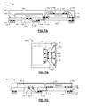
- FIG. 1A is a schematic of an integrated circuit (IC) package
- FIG. 1B is a schematic of a stacked IC package
- FIG. 2A is a schematic of a window IC package
- FIG. 2B is a schematic of a window IC package viewed from a window PCB bonding surface
- FIG. 3 is a schematic of a package-on-package stack
- FIG. 4 is a schematic of a stacked window IC package according to the present disclosure.
- FIG. 5A is a schematic of a single-sided window IC package according to the present disclosure.
- FIG. 5B is a schematic of a single-sided window IC package viewed from a window bonding surface according to the present disclosure
- FIG. 6A is a schematic of a fan-out window IC package according to the present disclosure.
- FIG. 6B is a schematic of a fan-out window IC package viewed from a window IC bonding surface according to the present disclosure
- FIG. 6C is a schematic of a fan-out window IC package viewed from a window IC bonding surface according to the present disclosure
- FIG. 7A is a schematic of a side-by-side window IC package according to the present disclosure.
- FIG. 7B is a schematic of a side-by-side window IC package viewed from a window IC bonding surface according to the present disclosure
- FIG. 7C is a schematic of a side-by-side window IC package including a flip chip IC according to the present disclosure
- FIG. 8A is a schematic of an inverted window IC package according to the present disclosure.
- FIG. 8B is a schematic of an inverted window IC package including a flip chip IC according to the present disclosure
- FIG. 8C is a schematic of an inverted window IC package including an alternative spacer according to the present disclosure.
- FIG. 9A is a schematic of an inverted window IC package including a single-sided inverted substrate according to the present disclosure.
- FIG. 9B is a schematic of an inverted window IC package including a single-sided inverted substrate and a flip chip IC according to the present disclosure
- FIG. 9C is a schematic of an inverted window IC package including a single-sided inverted substrate and an alternative spacer according to the present disclosure
- FIG. 10A is a schematic of an inverted window IC package including a flip chip IC located on top of a window IC and another IC according to the present disclosure.
- FIG. 10B is a schematic of an inverted window IC package including a flip chip IC located on top of a window IC according to the present disclosure.
- the stacked IC package 150 includes the spacer 156 between the top IC 152 and the bottom IC 154 .
- the spacer 156 provides clearance for the bonding wires 126 when the top IC 152 covers the bond pads 124 of the bottom IC 154 .
- the spacer 156 increases thickness of the stacked IC package 150 .
- a stacked window IC package according to the present disclosure eliminates the spacer 156 . Therefore, the stacked window IC package according to the present disclosure may be thinner than the stacked IC package 150 .
- the stacked window IC package includes an opening in a package substrate.
- the top surface of the bottom IC may be attached to the package substrate.
- the bottom surface of the bottom IC may be attached to the bottom surface of the top IC.
- the bottom IC may be connected to the top IC through the opening.
- the stacked window IC package of the present disclosure may reduce a length of connections between the top IC and the bottom IC.
- the bottom IC may connect to the package substrate on a single side of the opening.
- the top IC may be offset towards the single side of the opening.
- the bottom IC and the top IC may communicate through the single side of the package substrate to reduce the length of connection between the top IC and the bottom IC.
- the shorter connection between the top IC and the bottom IC may reduce an amount of termination resistance used for impedance matching between the top IC and the bottom IC.
- the reduction in termination resistance may reduce power consumption of the stacked window IC package.
- the shorter connection may reduce crosstalk and signal noise.
- the shorter connection may also provide for shorter wire bonds that have a reduced probability of mechanical failure.
- FIG. 4 shows a stacked window IC package that includes a window IC that is connected to a second IC through a substrate window.
- FIGS. 5A and 5B show a stacked window IC package that includes a window IC that is connected to a second IC through a single side of the substrate window.
- FIGS. 6A , 6 B, and 6 C show a fan-out window IC package including a fan-out substrate used to reduce bonding wire length.
- FIGS. 7A , 7 B, and 7 C show a side-by-side window IC package including a window IC and a second IC attached to a substrate having connections on a single side of the substrate window.
- the side-by-side window IC package includes a portion of bond pads between the second IC and the window IC.
- FIGS. 8A , 8 B, and 8 C show an inverted window IC package including an inverted substrate.
- FIGS. 9A , 9 B, and 9 C show an inverted window IC package including an inverted substrate having connections on a single side of the substrate window.
- FIGS. 10A and 10B show an inverted window IC package including a flip chip IC.
- a stacked window IC package 400 includes a window substrate 402 , the window IC 202 , and a second IC 404 .
- the window substrate 402 includes a window bonding surface 406 , the substrate window 208 , and a window IC bonding surface 408 .
- the window bonding surface 406 may include the PCB bond pads 114 and the window bond pads 212 .
- the window IC bonding surface 408 includes the substrate bond pads 118 .
- the substrate bond pads 118 may be located at a periphery of the window substrate 402 .
- the window IC 202 includes the window IC top surface and the window IC bottom surface.
- the window IC top surface is attached to the window IC bonding surface 408 .
- the window IC top surface includes the window IC bond pads 218 .
- the window IC bond pads 218 are accessible through the substrate window 208 .
- the window IC bond pads 218 may connect to the window bond pads 212 using bonding wires 126 that pass through the substrate window 208 .
- the window bond pads 212 may connect to the PCB bond pads 114 through the substrate interconnects 112 .
- the window bond pads 212 , the window IC bond pads 218 , and the substrate window 208 may be covered with the encapsulant 106 (e.g., epoxy).
- the IC bottom surface of the second IC 404 is attached to the window IC bottom surface.
- the IC bottom surface of the second IC 404 may be attached to the window IC bottom surface using any suitable adhesive.
- the suitable adhesive may include a die attach paste or a die bonding film.
- the stacked window IC package 400 allows for integration of multiple ICs in a package having a reduced profile.
- profile refers to the thickness or height of the package due to the stacking of the ICs, substrates, spacers, and encapsulant.
- the stacked window IC package 400 may have a reduced profile relative to the stacked IC package 150 .
- the stacked IC package 150 may include the spacer 156 that increases thickness of the stacked IC package 150
- the stacked window IC package 400 may eliminate the spacer 156 .
- the IC top surface of the second IC 404 includes second IC bond pads 410 - 1 , 410 - 2 , . . . , and 410 - n (collectively second IC bond pads 410 ).
- the second IC bond pads 410 may connect to the substrate bond pads 118 using bonding wires 126 .
- the second IC bond pads 410 , the window IC bond pads 218 , and the PCB bond pads 114 may be connected in numerous ways.
- the second IC bond pads 410 may connect to the window IC bond pads 218 and the PCB bond pads 114 through the substrate interconnects 112 .
- the window IC bond pads 218 may connect to the PCB bond pads 114 through the substrate interconnects 112 .
- the stacked window IC package 400 may include a memory IC and a system-on-chip (SoC).
- the window IC 202 may be the memory IC
- the second IC 404 may be the SoC.
- the memory IC may include a dynamic random access memory (DRAM) IC.
- the DRAM IC may be attached to the window IC bonding surface 408 .
- the bond pads of the DRAM IC may be accessible through the substrate window 208 .
- the SoC may communicate with the DRAM IC through the substrate interconnects 112 .
- the stacked window IC package 400 may be connected to a PCB that includes other IC packages and/or discrete components.
- the SoC may communicate with other IC packages and/or discrete components on the PCB.
- the other IC packages and/or discrete components on the PCB may also communicate with the DRAM IC through the substrate interconnects 112 .
- the stacked window IC package 400 may include memory ICs.
- the stacked window IC package 400 may include the DRAM IC and a non-volatile memory IC (e.g., flash memory).
- the window IC 202 may be the DRAM IC
- the second IC 404 may be the non-volatile memory IC.
- the memory ICs in the stacked window IC package 400 may have a reduced package profile.
- Other IC packages and/or discrete components on the PCB may communicate with the memory ICs.
- the single-sided window IC package 500 includes the window IC 202 , the second IC 404 , and a single-sided window substrate 502 .
- the single-sided window substrate 502 includes the window bond pads 212 along a single side of the substrate window 208 .
- a side of the single-sided window substrate 502 including the window bond pads 212 may be called a “bonding side” of the single-sided window substrate 502 .
- a side of the single-sided window substrate 502 that does not include the window bond pads 212 may be called a “non-bonding side” of the single-sided window substrate 502 .
- the bonding side and the non-bonding side are shown in detail in FIG. 5B .
- the bonding wires 126 connect the window IC bond pads 218 to the window bond pads 212 .
- the window bond pads 212 connect to the PCB bond pads 114 and the substrate bond pads 118 through the substrate interconnects 112 .
- the second IC 404 may connect to the PCB bond pads 114 and the window IC 202 through the substrate interconnects 112 .
- the window bond pads 212 are located along a single side of the perimeter 220 of the substrate window 208 (i.e., the bonding side). While the perimeter 220 shown is a rectangle, other shapes are anticipated.
- the bonding wires 126 connect the window bond pads 212 to the window IC bond pads 218 . While the window IC bond pads 218 of FIG. 5B are organized in two rows, other layouts are anticipated.
- the window bond pads 212 may connect to the PCB bond pads 114 and solder balls 116 through substrate interconnects 112 on the window bonding surface 406 .
- the window bond pads 212 may also connect to the second IC 404 through substrate interconnects 112 that pass from the window bonding surface 406 to the window IC bonding surface 408 as indicated at 504 .
- the fan-out window IC package 700 includes the single-sided window substrate 502 , the window IC 202 , the second IC 404 , and a fan-out substrate 702 .
- the fan-out window IC package 700 may include the window substrate 402 in place of the single-sided window substrate 502 .
- the fan-out substrate 702 includes fan-out bond pads 704 - 1 , 704 - 2 , . . . , and 704 - n (collectively fan-out bond pads 704 ) and the substrate interconnects 112 .
- the fan-out substrate 702 may be a single or multi-layered structure that includes conductive traces and vias that connect the fan-out bond pads 704 .
- the fan-out substrate 702 may include a single or multi-layered PCB.
- the substrate interconnects 112 may connect the fan-out bond pads 704 .
- the fan-out substrate 702 is attached to the window IC bottom surface.
- the fan-out substrate 702 is positioned adjacent to the second IC 404 .
- the bonding wires 126 connect the second IC bond pads 410 to the fan-out bond pads 704 .
- the bonding wires 126 that connect the fan-out bond pads 704 to the second IC 404 and the bonding wires 126 that connect the fan-out substrate 702 to the substrate bond pads 118 may be called “fan-out bonding wires.”
- the fan-out bond pads 704 are connected to the substrate bond pads 118 using bonding wires 126 .
- the fan-out substrate 702 may reduce the length of the bonding wires 126 that connect the second IC bond pads 410 to the substrate bond pads 118 . For example, the fan-out bonding wires may be shorter than bonding wires that would otherwise be needed to connect the second IC bond pads 410 directly with the substrate bond pads 118 .
- the fan-out substrate 702 is adjacent to the second IC 404 .
- the outline of the fan-out substrate 702 is similar to the outline of the second IC 404 .
- the second IC bond pads 410 may be connected to the substrate bond pads 118 using two fan-out bonding wires 126 and the substrate interconnects 112 of the fan-out substrate 702 .
- the second IC bond pads 410 may also be connected to the substrate bond pads 118 using the short bonding wires 602 when a distance between the second IC bond pads 410 and the substrate bond pads 118 allows.
- the fan out substrate 702 is placed adjacent to the second IC 404 .
- the outline of the second IC 404 is smaller than the outline of the fan-out substrate 702 .
- the term “outline” refers to the length and width of the IC top/bottom surfaces. In other words, the term “outline” refers to the area of the IC.
- the bonding wires of different lengths may be described as short bonding wires and long bonding wires.
- the terms “short” and “long” may describe the relative lengths of the bonding wires.
- FIG. 6B and FIG. 6C depict the second IC 404 with a similar/smaller outline than the fan-out substrate 702 , respectively, the second IC 404 may have a larger outline than the fan-out substrate 702 .
- the fan-out window IC package 700 may include the DRAM IC and the SoC.
- the DRAM IC may be attached to the single-sided window substrate 502 and the SoC may be attached to the DRAM IC.
- the DRAM IC may include rows of bond pads that are centrally located on the top surface of the DRAM IC. The rows of bond pads are accessible through the substrate window 208 .
- the bond pads of the DRAM IC may be connected to the window bond pads 212 .
- the SoC may have a smaller outline than the DRAM IC and therefore may be offset towards the bonding side of the single-sided window substrate 502 . The offset of the SoC towards the bonding side allows the SoC to be attached to the single-sided window substrate 502 using short bonding wires 602 .
- the DRAM IC may communicate with the SoC through the short bonding wires 602 .
- Connection of the SoC and the DRAM IC using short bonding wires 602 reduces an amount of termination resistance used for impedance matching between the DRAM IC and the SoC.
- the reduction in termination resistance may reduce power dissipation of the fan-out window IC package 700 .
- the shorter connection between the DRAM IC and the SoC may reduce crosstalk and signal noise.
- a side-by-side window IC package 900 includes the window IC 202 , the second IC 404 , the single-sided window substrate 502 , and the encapsulant 106 .
- the window substrate 402 may be used instead of the single-sided window substrate 502 .
- the single-sided window substrate 502 includes the window bonding surface 406 and the window IC bonding surface 408 .
- the window bonding surface 406 includes the window bond pads 212 and the PCB bond pads 114 .
- the window IC bonding surface 408 includes the substrate bond pads 118 .
- the window IC top surface is attached to the window IC bonding surface 408 so that the window IC bond pads 218 are accessible through the substrate window 208 .
- the IC bottom surface of the second IC 404 is attached to the window IC bonding surface 408 .
- the second IC 404 is attached to the window IC bonding surface 408 adjacent to the window IC 202 .
- a plurality of the substrate bond pads 118 is located between the window IC 202 and the second IC 404 .
- a substrate bond pad 118 included in the plurality of the substrate bond pads 118 is called a substrate bond pad 902 .
- the window bond pads 212 connect to the substrate bond pads 902 through the substrate interconnects 112 .
- the second IC 404 connects to the substrate bond pads 902 using short bonding wires 602 .
- the window IC bond pads 218 may be connected to the window bond pads 212 using bonding wires 126 .
- the second IC bond pads 410 may be connected to the substrate bond pads 118 using bonding wires 126 .
- FIG. 7B an exemplary layout of the substrate bond pads 902 is shown.
- the outline of the second IC 404 is smaller than the outline of the window IC 202 , other outlines are anticipated.
- the outline of the window IC 202 may be similar to or smaller than the outline of the second IC 404 .
- the window IC 202 and the second IC 404 may be connected in numerous ways.
- the window IC 202 may connect to the PCB bond pads 114 and the substrate bond pads 118 , 902 .
- the second IC 404 may connect to the PCB bond pads 114 and the substrate bond pads 118 , 902 .
- the second IC 404 and the window IC 202 may communicate through the substrate interconnects 112 and the substrate bond pads 902 .
- the second IC 404 and the window IC 202 may communicate only through the substrate bond pads 902 .
- the side-by-side window IC package 900 may include the DRAM IC and the SoC.
- the DRAM IC and the SoC may be attached to the window IC bonding surface 408 of the single-sided window substrate 502 .
- the DRAM IC may include rows of bond pads that are accessible through the substrate window 208 .
- the bond pads of the DRAM IC may be connected to the window bond pads 212 .
- the SoC may connect to the DRAM IC through the substrate bond pads 902 .
- the SoC may be proximate to the substrate bond pads 902 to reduce the length of the short bonding wires 602 .
- the bond pads on the SoC that connect to the substrate bond pads 902 may also be proximate to the substrate bond pads 902 to further reduce the length of the short bonding wires 602 .
- the side-by-side window IC package 900 reduces the length of the short bonding wires 602 used to connect the DRAM IC and the SoC.
- the side-by-side window IC package 900 also provides a package with a reduced profile.
- a side-by-side window IC package 904 includes the second IC 404 in a flip chip configuration.
- the second IC bond pads 410 may be connected to the substrate bond pads 118 in the flip chip configuration. In the flip chip configuration, the second IC bond pads 410 may be connected to the substrate bond pads 118 using solder balls 116 .
- the second IC 404 may also be attached to the single-sided window substrate 502 using any suitable adhesive. For example, the second IC 404 may be underfilled with any suitable adhesive.
- the second IC 404 may communicate with the window IC 202 through the substrate bond pads 118 that are nearest to the window bond pads 212 to provide a short connection length.
- the second IC 404 in the flip chip configuration may have a reduced outline and a reduced profile relative to the second IC 404 that is connected using short bonding wires 602 .
- the reduced outline and the reduced profile of the second IC 404 in the flip chip configuration may allow for a reduced package outline and a reduced package profile.
- an inverted window IC package 1000 includes the package substrate 102 , the second IC 404 , the spacer 156 , the window IC 202 , and an inverted window substrate 1002 .
- the IC bottom surface of the second IC 404 is attached to the IC bonding surface 110 of the package substrate 102 .
- the spacer 156 is attached to the IC top surface of the second IC 404 .
- the window IC bottom surface is attached to the spacer 156 .
- the inverted window substrate 1002 includes the window IC bonding surface 408 and the window bonding surface 406 .
- the window IC bonding surface 408 of the inverted window substrate 1002 is attached to the window IC top surface.
- the window bonding surface 406 of the inverted window substrate 1002 includes the substrate bond pads 118 and the window bond pads 212 .
- the window IC bond pads 218 are connected to the window bond pads 212 using bonding wires 126 .
- the window bond pads 212 are connected to the substrate bond pads 118 of the inverted window substrate 1002 through the substrate interconnects 112 of the inverted window substrate 1002 .
- the substrate bond pads 118 of the inverted window substrate 1002 are connected to the substrate bond pads 118 of the package substrate 102 using bonding wires 126 .
- the second IC bond pads 410 are connected to the substrate bond pads 118 of the package substrate 102 using bonding wires 126 .
- the window IC 202 may be connected to the second IC 404 and the PCB bond pads 114 of the package substrate 102 through the substrate interconnects 112 of the package substrate 102 .
- the second IC 404 may connect to the PCB bond pads 114 of the package substrate 102 through the substrate interconnects 112 of the package substrate 102 .
- the second IC 404 may be connected in the flip chip configuration.
- the IC bottom surface of the second IC 404 may be attached to the window IC bottom surface when the second IC 404 is connected to the package substrate 102 in the flip chip configuration.
- An inverted window IC package 1006 including the second IC 404 in the flip chip configuration may eliminate the spacer 156 . Accordingly, the inverted window IC package 1006 may have a reduced package profile relative to the inverted window IC package 1000 .
- an inverted window IC package 1008 includes an alternative spacer 1004 .
- the alternative spacer 1004 may support the window IC 202 when the outline of the second IC 404 is such that the spacer 156 will not support the window IC 202 .
- the alternative spacer 1004 may include two separate spacer portions to support the window IC 202 .
- the alternative spacer 1004 may also include a ring around the second IC 404 .
- the second IC 404 may be an SoC
- the window IC 202 may be a DRAM IC.
- the outline of the DRAM IC may be larger than the outline of the SoC. Accordingly, the alternative spacer 1004 may be used to support the larger DRAM IC.
- an inverted window IC package 1100 includes a single-sided inverted substrate 1102 .
- the single-sided inverted substrate 1102 includes the window bond pads 212 and the substrate bond pads 118 on the bonding side of the single-sided inverted substrate 1102 .
- the substrate bond pads 118 and the window bond pads 212 of the single-sided inverted substrate 1102 are connected through the substrate interconnects 112 .
- the substrate bond pads 118 of the single-sided inverted substrate 1102 may connect to the substrate bond pads 118 of the package substrate 102 using bonding wires 126 .
- the window IC bond pads 218 may connect to the second IC bond pads 410 and the PCB bond pads 114 through the substrate interconnects 112 of the package substrate 102 .
- the second IC bond pads 410 may connect to the PCB bond pads 114 through the bonding wires 126 and the substrate interconnects 112 of the package substrate 102 .
- the second IC 404 may be connected in the flip chip configuration.
- the IC bottom surface of the second IC 404 may be attached to the window IC bottom surface when the second IC 404 is connected in the flip chip configuration.
- the inverted window IC package 1104 including the second IC 404 in the flip chip configuration may eliminate the spacer 156 . Accordingly, the inverted window IC package 1104 may have a reduced package profile relative to the inverted window IC package 1100 .
- an inverted window IC package 1106 includes an alternative spacer 1004 .
- the alternative spacer 1004 may support the window IC 202 when the outline of the second IC 404 is such that the spacer 156 will not support the window IC 202 .
- the alternative spacer 1004 may include two separate spacer portions to support the window IC 202 .
- the alternative spacer 1004 may also include a ring around the second IC 404 , or any other suitable spacer or spacers.
- an inverted window IC package 1200 includes the window IC 202 , the window substrate 1202 , the second IC 404 , a third IC 1204 and the package substrate 102 .
- the second IC 404 and the window substrate 1202 are coupled as shown in a flip chip configuration, with the second IC 404 located on top of the window substrate 1202 .
- the window IC 202 , the third IC 1204 and the package substrate 102 are arranged in a stacked configuration as shown.
- the third IC 1204 may include a SoC or other types of integrated circuit devices.
- an inverted window IC package 1300 is shown.
- the inverted window IC package 1300 does not include the third IC 1204 .
- the second IC 404 is similarly located on top of the window substrate 1202 in a flip chip configuration.
Abstract
An integrated circuit (IC) package including a substrate, a first IC, and a second IC adjacent to the first IC. The substrate includes first and second surfaces respectively having first and second bond pads, and an opening offset relative to a center of the substrate and extending from the first surface to the second surface. The first IC includes a third surface having third bond pads accessible through the opening. The second IC includes fourth and fifth surfaces respectively having fourth and fifth bond pads. The third and fifth surfaces are attached to the second surface. At least one of the third bond pads is connected to at least one of the first bond pads using one or more bond wires extending through the opening. At least one of the fourth bond pads is connected to at least one of the second bond pads using one or more bond wires.
Description
This application is a continuation of U.S. patent application Ser. No. 12/565,430, filed Sep. 23, 2009, which claims the benefit of U.S. Provisional Application Nos. 61/099,355, filed Sep. 23, 2008 and 61/121,018, filed Dec. 9, 2008. The entire disclosures of the above applications are incorporated herein by reference.
The present disclosure relates to integrated circuit packages, and more particularly to integrated circuit packages including multiple integrated circuits stacked on a window substrate.
The background description provided herein is for the purpose of generally presenting the context of the disclosure. Work of the presently named inventors, to the extent the work is described in this background section, as well as aspects of the description that may not otherwise qualify as prior art at the time of filing, are neither expressly nor impliedly admitted as prior art against the present disclosure.
An integrated circuit (IC) package includes an IC. The IC may include analog and/or digital circuits. Analog circuits may include, but are not limited to, operational amplifiers, sensors, and analog-to-digital converters. Digital circuits may include, but are not limited to, combinational logic, microprocessors, memory, and external interface circuits. The IC may include a system-on-chip (SoC) that includes multiple analog/digital circuits. For example, the SoC may include microprocessors, memory, analog-to-digital converters, and operational amplifiers.
The IC may be attached to a substrate. Throughout the disclosure, the term “attach” refers to a bonding of two surfaces with a bonding material. For example, a die attach paste may attach a surface of the IC to a surface of the substrate. The IC may be connected to IC package leads and may be encapsulated. The IC package leads typically connect the IC to a printed circuit board (PCB). The PCB may include other IC packages and/or discrete components that may communicate with the IC.
Referring now to FIG. 1A , an IC package 100 includes a package substrate 102, an IC 104, and an encapsulant 106. The package substrate 102 includes a PCB bonding surface 108, an IC bonding surface 110, and substrate interconnects 112. The PCB bonding surface 108 includes PCB bond pads 114-1, 114-2, . . . , and 114-n (collectively PCB bond pads 114). The IC 104 may connect to the PCB or another IC (both not shown) through the PCB bond pads 114.
The PCB bond pads 114 may be connected to the PCB using solder balls 116-1, 116-2, . . . , and 116-n (collectively solder balls 116). The PCB bond pads 114 and the solder balls 116 may include any bonding structure suitable for connecting the IC package 100 to the PCB or to another IC package. For example only, the PCB bond pads 114 and the solder balls 116 may include a ball grid array (BGA) with solder balls 116. The PCB bond pads 114 and the solder balls 116 may also include a land grid array (LGA) without solder balls 116.
The IC bonding surface 110 includes substrate bond pads 118-1, 118-2, . . . , and 118-n (collectively substrate bond pads 118). The substrate bond pads 118 are connected to the PCB bond pads 114 through the substrate interconnects 112. The substrate interconnects 112 include conductive traces and conductive vias that are integral to the package substrate 102. The package substrate 102 may include a single layer of conductive traces or multiple layers of conductive traces. For example only, the conductive traces may be located on the PCB bonding surface 108 and the IC bonding surface 110. The conductive vias may connect the conductive traces of the PCB bonding surface 108 and the conductive traces of the IC bonding surface 110.
The IC 104 includes an IC top surface 120 and an IC bottom surface 122. The IC bottom surface 122 is attached to the IC bonding surface 110 of the package substrate 102. The IC 104 may be attached to the package substrate 102 using any suitable adhesive. For example only, the adhesive may include a die attach paste or a die bonding film. The IC top surface 120 includes IC bond pads 124-1, 124-2, . . . , and 124-n (collectively IC bond pads 124). The IC bond pads 124 are connected to the substrate bond pads 118 using bonding wires 126-1, 126-2, . . . , and 126-n (collectively bonding wires 126). The IC 104 is covered with the encapsulant 106. The encapsulant 106 protects the IC 104 from physical damage and corrosion. The encapsulant 106 may be ceramic or polymer based.
The IC bond pads 124 may be connected to the PCB bond pads 114 in numerous ways. A single IC bond pad 124 may be connected to a single PCB bond pad 114. A single IC bond pad 124 may be connected to a plurality of the PCB bond pads 114. A plurality of the IC bond pads 124 may be connected to a single PCB bond pad 114.
Throughout the disclosure the term “top surface” refers to a surface of an IC that includes IC bond pads 124. Throughout the disclosure the term “bottom surface” refers to a surface of the IC that may not include IC bond pads 124. For example, as shown in FIG. 1A , the IC top surface 120 includes IC bond pads 124 and the IC bottom surface 122 does not include IC bond pads 124.
Referring now to FIG. 1B , a stacked IC package 150 includes the package substrate 102, a top IC 152, a bottom IC 154, and a spacer 156. The IC bottom surface of the bottom IC 154 is attached to the IC bonding surface 110 of the package substrate 102. The spacer 156 is attached to the IC top surface of the bottom IC 154 and the IC bottom surface of the top IC 152. The spacer 156 provides structural support for the top IC 152. The spacer 156 may also provide clearance for the bonding wires 126 that connect the bottom IC 154 to the substrate bond pads 118. The spacer 156 may include an insulating material such as oxidized silicon.
The IC bond pads 124 of the top IC 152, the IC bond pads 124 of the bottom IC 154, and the PCB bond pads 114 of the package substrate 102 may be connected in numerous ways. The IC bond pads 124 of the top IC 152 may be connected to the IC bond pads 124 of the bottom IC 154 through the substrate interconnects 112. The IC bond pads 124 of the top IC 152 may be connected to the PCB bond pads 114 through the substrate interconnects 112. The IC bond pads 124 of the bottom IC 154 may be connected to the PCB bond pads 114 through the substrate interconnects 112.
Referring now to FIG. 2A , a window IC package 200 includes a package substrate 204 having a window 208. The package substrate 204 is hereinafter called a window package substrate 204. The window 208 is hereinafter called a substrate window 208. The window IC package 200 further includes an IC 202 that is attached to the window package substrate 204. The IC 202 is hereinafter called a window IC 202. The encapsulant 106 encapsulates the window package substrate 204 and the window IC 202.
The window package substrate 204 includes a window PCB bonding surface 206 and a package IC bonding surface 210. The window PCB bonding surface 206 may include the PCB bond pads 114 and window bond pads 212. The substrate window 208 is an opening defined by the window package substrate 204. The substrate window 208 extends from the window PCB bonding surface 206 to the package IC bonding surface 210. The substrate window 208 allows for connection of the window bond pads 212 to the window IC 202 using bonding wires 126.
The window IC 202 includes a window IC top surface 214 and a window IC bottom surface 216. The window IC top surface 214 is attached to the package IC bonding surface 210. The window IC top surface 214 includes window IC bond pads 218. The window IC bond pads 218 are accessible through the substrate window 208. The window IC bond pads 218 may be connected to the window bond pads 212 using bonding wires 126 that pass through the substrate window 208. The window bond pads 212 may be connected to the PCB bond pads 114 through the substrate interconnects 112. The window bond pads 212, the window IC bond pads 218, and the substrate window 208 may be covered by the encapsulant 106. For example only, the encapsulant 106 may include an epoxy.
Throughout the disclosure, the term “window IC top surface” refers to a surface of the window IC 202 that includes window IC bond pads 218. Throughout the disclosure, the term “window IC bottom surface” refers to a surface of the window IC 202 that may not include window IC bond pads 218. For example, as shown in FIG. 2A , the window IC top surface 214 includes the window IC bond pads 218 and the window IC bottom surface 216 does not include the window IC bond pads 218.
Referring now to FIG. 2B , the window bond pads 212 are located at a perimeter 220 of the substrate window 208. The window bond pads 212 are connected to the window IC bond pads 218 using bonding wires 126. The window bond pads 212 are connected to the PCB bond pads 114 and solder balls 116 on two sides of the perimeter 220 through the substrate interconnects 112.
Referring now to FIG. 3 , ICs may be stacked in a package-on-package (PoP) configuration. A PoP stack 300 includes a top IC package 302 and a bottom IC package 304. The bottom IC package 304 includes the package substrate 102, the IC 104, the spacer 156, and a PoP substrate 306. The IC bottom surface of the IC 104 is attached to the IC bonding surface 110 of the package substrate 102. The spacer 156 is attached to the IC top surface of the IC 104. The PoP substrate 306 is attached to the spacer 156.
The PoP substrate 306 includes PoP substrate bond pads 310 and the substrate interconnects 112. The solder balls 116 may connect the PCB bond pads 114 of the top IC package 302 to the PoP substrate bond pads 310. The bonding wires 126 may connect the PoP substrate bond pads 310 to the substrate bond pads 118. An IC of the top IC package 302 may connect to the IC 104 and the PCB bond pads 114 of the package substrate 102 through the substrate interconnects 112 of the package substrate 102. The IC 104 may connect to the PCB bond pads 114 of the package substrate 102 through the substrate interconnects 112 of the package substrate 102.
An integrated circuit (IC) package is disclosed. The IC package includes a first substrate having a first surface having first substrate bond pads, a second surface having second substrate bond pads, and an opening that extends from the first surface to the second surface. The IC package further includes a first IC having a first IC surface that includes first bond pads and that is directly attached to the second surface of the first substrate, and a second IC surface. The first bond pads are accessible through the opening. The IC package also includes a second IC having a third IC surface that is directly attached to the second IC surface, and a fourth IC surface that includes second bond pads. At least one of the first bond pads is connected to at least one of the first substrate bond pads using one or more bond wires. At least one of the second bond pads is connected to at least one of the second substrate bond pads using one or more bond wires. The opening has a first side and a second side. The first substrate bond pads are located adjacent to only the first side of the opening.
Further areas of applicability of the present disclosure will become apparent from the detailed description, the claims and the drawings. The detailed description and specific examples are intended for purposes of illustration only and are not intended to limit the scope of the disclosure.
The present disclosure will become more fully understood from the detailed description and the accompanying drawings, wherein:
The following description is merely exemplary in nature and is in no way intended to limit the disclosure, its application, or uses. For purposes of clarity, the same reference numbers will be used in the drawings to identify similar elements. As used herein, the phrase at least one of A, B, and C should be construed to mean a logical (A or B or C), using a non-exclusive logical or. It should be understood that steps within a method may be executed in different order without altering the principles of the present disclosure.
Typically, as shown in FIG. 1B , the stacked IC package 150 includes the spacer 156 between the top IC 152 and the bottom IC 154. The spacer 156 provides clearance for the bonding wires 126 when the top IC 152 covers the bond pads 124 of the bottom IC 154. The spacer 156 increases thickness of the stacked IC package 150. A stacked window IC package according to the present disclosure eliminates the spacer 156. Therefore, the stacked window IC package according to the present disclosure may be thinner than the stacked IC package 150.
Additionally, the stacked window IC package according to the present disclosure includes an opening in a package substrate. The top surface of the bottom IC may be attached to the package substrate. The bottom surface of the bottom IC may be attached to the bottom surface of the top IC. The bottom IC may be connected to the top IC through the opening.
The stacked window IC package of the present disclosure may reduce a length of connections between the top IC and the bottom IC. The bottom IC may connect to the package substrate on a single side of the opening. The top IC may be offset towards the single side of the opening. The bottom IC and the top IC may communicate through the single side of the package substrate to reduce the length of connection between the top IC and the bottom IC.
The shorter connection between the top IC and the bottom IC may reduce an amount of termination resistance used for impedance matching between the top IC and the bottom IC. The reduction in termination resistance may reduce power consumption of the stacked window IC package. Additionally, the shorter connection may reduce crosstalk and signal noise. The shorter connection may also provide for shorter wire bonds that have a reduced probability of mechanical failure.
Before a more detailed discussion, a brief description of the drawings is presented. FIG. 4 shows a stacked window IC package that includes a window IC that is connected to a second IC through a substrate window. FIGS. 5A and 5B show a stacked window IC package that includes a window IC that is connected to a second IC through a single side of the substrate window. FIGS. 6A , 6B, and 6C show a fan-out window IC package including a fan-out substrate used to reduce bonding wire length. FIGS. 7A , 7B, and 7C show a side-by-side window IC package including a window IC and a second IC attached to a substrate having connections on a single side of the substrate window. The side-by-side window IC package includes a portion of bond pads between the second IC and the window IC. FIGS. 8A , 8B, and 8C show an inverted window IC package including an inverted substrate. FIGS. 9A , 9B, and 9C show an inverted window IC package including an inverted substrate having connections on a single side of the substrate window. FIGS. 10A and 10B show an inverted window IC package including a flip chip IC.
Referring now to FIG. 4 , a stacked window IC package 400 includes a window substrate 402, the window IC 202, and a second IC 404. The window substrate 402 includes a window bonding surface 406, the substrate window 208, and a window IC bonding surface 408. The window bonding surface 406 may include the PCB bond pads 114 and the window bond pads 212. The window IC bonding surface 408 includes the substrate bond pads 118. The substrate bond pads 118 may be located at a periphery of the window substrate 402.
The window IC 202 includes the window IC top surface and the window IC bottom surface. The window IC top surface is attached to the window IC bonding surface 408. The window IC top surface includes the window IC bond pads 218. The window IC bond pads 218 are accessible through the substrate window 208. The window IC bond pads 218 may connect to the window bond pads 212 using bonding wires 126 that pass through the substrate window 208. The window bond pads 212 may connect to the PCB bond pads 114 through the substrate interconnects 112. The window bond pads 212, the window IC bond pads 218, and the substrate window 208 may be covered with the encapsulant 106 (e.g., epoxy).
The IC bottom surface of the second IC 404 is attached to the window IC bottom surface. The IC bottom surface of the second IC 404 may be attached to the window IC bottom surface using any suitable adhesive. For example only, the suitable adhesive may include a die attach paste or a die bonding film.
The stacked window IC package 400 allows for integration of multiple ICs in a package having a reduced profile. The term “profile” refers to the thickness or height of the package due to the stacking of the ICs, substrates, spacers, and encapsulant. The stacked window IC package 400 may have a reduced profile relative to the stacked IC package 150. For example, while the stacked IC package 150 may include the spacer 156 that increases thickness of the stacked IC package 150, the stacked window IC package 400 may eliminate the spacer 156.
The IC top surface of the second IC 404 includes second IC bond pads 410-1, 410-2, . . . , and 410-n (collectively second IC bond pads 410). The second IC bond pads 410 may connect to the substrate bond pads 118 using bonding wires 126. The second IC bond pads 410, the window IC bond pads 218, and the PCB bond pads 114 may be connected in numerous ways. The second IC bond pads 410 may connect to the window IC bond pads 218 and the PCB bond pads 114 through the substrate interconnects 112. The window IC bond pads 218 may connect to the PCB bond pads 114 through the substrate interconnects 112.
The stacked window IC package 400 may include a memory IC and a system-on-chip (SoC). The window IC 202 may be the memory IC, and the second IC 404 may be the SoC. For example only, the memory IC may include a dynamic random access memory (DRAM) IC. The DRAM IC may be attached to the window IC bonding surface 408. The bond pads of the DRAM IC may be accessible through the substrate window 208. The SoC may communicate with the DRAM IC through the substrate interconnects 112. The stacked window IC package 400 may be connected to a PCB that includes other IC packages and/or discrete components. The SoC may communicate with other IC packages and/or discrete components on the PCB. The other IC packages and/or discrete components on the PCB may also communicate with the DRAM IC through the substrate interconnects 112.
Alternatively, the stacked window IC package 400 may include memory ICs. For example only, the stacked window IC package 400 may include the DRAM IC and a non-volatile memory IC (e.g., flash memory). The window IC 202 may be the DRAM IC, and the second IC 404 may be the non-volatile memory IC. The memory ICs in the stacked window IC package 400 may have a reduced package profile. Other IC packages and/or discrete components on the PCB may communicate with the memory ICs.
Referring now to FIGS. 5A and 5B , a single-sided window IC package 500 is shown. In FIGS. 5A and 5B , the single-sided window IC package 500 includes the window IC 202, the second IC 404, and a single-sided window substrate 502. The single-sided window substrate 502 includes the window bond pads 212 along a single side of the substrate window 208. A side of the single-sided window substrate 502 including the window bond pads 212 may be called a “bonding side” of the single-sided window substrate 502. A side of the single-sided window substrate 502 that does not include the window bond pads 212 may be called a “non-bonding side” of the single-sided window substrate 502. The bonding side and the non-bonding side are shown in detail in FIG. 5B . The bonding wires 126 connect the window IC bond pads 218 to the window bond pads 212. The window bond pads 212 connect to the PCB bond pads 114 and the substrate bond pads 118 through the substrate interconnects 112. The second IC 404 may connect to the PCB bond pads 114 and the window IC 202 through the substrate interconnects 112.
In FIG. 5B , the window bond pads 212 are located along a single side of the perimeter 220 of the substrate window 208 (i.e., the bonding side). While the perimeter 220 shown is a rectangle, other shapes are anticipated. The bonding wires 126 connect the window bond pads 212 to the window IC bond pads 218. While the window IC bond pads 218 of FIG. 5B are organized in two rows, other layouts are anticipated.
As shown in FIG. 5B , the window bond pads 212 may connect to the PCB bond pads 114 and solder balls 116 through substrate interconnects 112 on the window bonding surface 406. The window bond pads 212 may also connect to the second IC 404 through substrate interconnects 112 that pass from the window bonding surface 406 to the window IC bonding surface 408 as indicated at 504.
Referring now to FIGS. 6A-6C , a fan-out window IC package 700 is shown. In FIG. 6A , the fan-out window IC package 700 includes the single-sided window substrate 502, the window IC 202, the second IC 404, and a fan-out substrate 702. Alternatively, the fan-out window IC package 700 may include the window substrate 402 in place of the single-sided window substrate 502. The fan-out substrate 702 includes fan-out bond pads 704-1, 704-2, . . . , and 704-n (collectively fan-out bond pads 704) and the substrate interconnects 112. The fan-out substrate 702 may be a single or multi-layered structure that includes conductive traces and vias that connect the fan-out bond pads 704. For example, the fan-out substrate 702 may include a single or multi-layered PCB. The substrate interconnects 112 may connect the fan-out bond pads 704. The fan-out substrate 702 is attached to the window IC bottom surface. The fan-out substrate 702 is positioned adjacent to the second IC 404.
The bonding wires 126 connect the second IC bond pads 410 to the fan-out bond pads 704. The bonding wires 126 that connect the fan-out bond pads 704 to the second IC 404 and the bonding wires 126 that connect the fan-out substrate 702 to the substrate bond pads 118 may be called “fan-out bonding wires.” The fan-out bond pads 704 are connected to the substrate bond pads 118 using bonding wires 126. The fan-out substrate 702 may reduce the length of the bonding wires 126 that connect the second IC bond pads 410 to the substrate bond pads 118. For example, the fan-out bonding wires may be shorter than bonding wires that would otherwise be needed to connect the second IC bond pads 410 directly with the substrate bond pads 118.
In FIG. 6B , the fan-out substrate 702 is adjacent to the second IC 404. The outline of the fan-out substrate 702 is similar to the outline of the second IC 404. The second IC bond pads 410 may be connected to the substrate bond pads 118 using two fan-out bonding wires 126 and the substrate interconnects 112 of the fan-out substrate 702. The second IC bond pads 410 may also be connected to the substrate bond pads 118 using the short bonding wires 602 when a distance between the second IC bond pads 410 and the substrate bond pads 118 allows.
In FIG. 6C , the fan out substrate 702 is placed adjacent to the second IC 404. The outline of the second IC 404 is smaller than the outline of the fan-out substrate 702. The term “outline” refers to the length and width of the IC top/bottom surfaces. In other words, the term “outline” refers to the area of the IC. The bonding wires of different lengths may be described as short bonding wires and long bonding wires. The terms “short” and “long” may describe the relative lengths of the bonding wires.
Although FIG. 6B and FIG. 6C depict the second IC 404 with a similar/smaller outline than the fan-out substrate 702, respectively, the second IC 404 may have a larger outline than the fan-out substrate 702.
The fan-out window IC package 700 may include the DRAM IC and the SoC. The DRAM IC may be attached to the single-sided window substrate 502 and the SoC may be attached to the DRAM IC. The DRAM IC may include rows of bond pads that are centrally located on the top surface of the DRAM IC. The rows of bond pads are accessible through the substrate window 208. The bond pads of the DRAM IC may be connected to the window bond pads 212. The SoC may have a smaller outline than the DRAM IC and therefore may be offset towards the bonding side of the single-sided window substrate 502. The offset of the SoC towards the bonding side allows the SoC to be attached to the single-sided window substrate 502 using short bonding wires 602.
The DRAM IC may communicate with the SoC through the short bonding wires 602. Connection of the SoC and the DRAM IC using short bonding wires 602 reduces an amount of termination resistance used for impedance matching between the DRAM IC and the SoC. The reduction in termination resistance may reduce power dissipation of the fan-out window IC package 700. Additionally, the shorter connection between the DRAM IC and the SoC may reduce crosstalk and signal noise.
Referring now to FIG. 7A , a side-by-side window IC package 900 includes the window IC 202, the second IC 404, the single-sided window substrate 502, and the encapsulant 106. Although not shown, the window substrate 402 may be used instead of the single-sided window substrate 502. The single-sided window substrate 502 includes the window bonding surface 406 and the window IC bonding surface 408. The window bonding surface 406 includes the window bond pads 212 and the PCB bond pads 114.
The window IC bonding surface 408 includes the substrate bond pads 118. The window IC top surface is attached to the window IC bonding surface 408 so that the window IC bond pads 218 are accessible through the substrate window 208. The IC bottom surface of the second IC 404 is attached to the window IC bonding surface 408. The second IC 404 is attached to the window IC bonding surface 408 adjacent to the window IC 202.
A plurality of the substrate bond pads 118 is located between the window IC 202 and the second IC 404. Hereinafter, a substrate bond pad 118 included in the plurality of the substrate bond pads 118 is called a substrate bond pad 902. The window bond pads 212 connect to the substrate bond pads 902 through the substrate interconnects 112. The second IC 404 connects to the substrate bond pads 902 using short bonding wires 602. The window IC bond pads 218 may be connected to the window bond pads 212 using bonding wires 126. The second IC bond pads 410 may be connected to the substrate bond pads 118 using bonding wires 126.
Referring now to FIG. 7B , an exemplary layout of the substrate bond pads 902 is shown. Although the outline of the second IC 404 is smaller than the outline of the window IC 202, other outlines are anticipated. For example, the outline of the window IC 202 may be similar to or smaller than the outline of the second IC 404.
The window IC 202 and the second IC 404 may be connected in numerous ways. The window IC 202 may connect to the PCB bond pads 114 and the substrate bond pads 118, 902. The second IC 404 may connect to the PCB bond pads 114 and the substrate bond pads 118, 902. The second IC 404 and the window IC 202 may communicate through the substrate interconnects 112 and the substrate bond pads 902. For example only, the second IC 404 and the window IC 202 may communicate only through the substrate bond pads 902.
The side-by-side window IC package 900 may include the DRAM IC and the SoC. The DRAM IC and the SoC may be attached to the window IC bonding surface 408 of the single-sided window substrate 502. The DRAM IC may include rows of bond pads that are accessible through the substrate window 208. The bond pads of the DRAM IC may be connected to the window bond pads 212. The SoC may connect to the DRAM IC through the substrate bond pads 902. The SoC may be proximate to the substrate bond pads 902 to reduce the length of the short bonding wires 602. The bond pads on the SoC that connect to the substrate bond pads 902 may also be proximate to the substrate bond pads 902 to further reduce the length of the short bonding wires 602. Thus, the side-by-side window IC package 900 reduces the length of the short bonding wires 602 used to connect the DRAM IC and the SoC. The side-by-side window IC package 900 also provides a package with a reduced profile.
Referring now to FIG. 7C , a side-by-side window IC package 904 includes the second IC 404 in a flip chip configuration. The second IC bond pads 410 may be connected to the substrate bond pads 118 in the flip chip configuration. In the flip chip configuration, the second IC bond pads 410 may be connected to the substrate bond pads 118 using solder balls 116. The second IC 404 may also be attached to the single-sided window substrate 502 using any suitable adhesive. For example, the second IC 404 may be underfilled with any suitable adhesive.
The second IC 404 may communicate with the window IC 202 through the substrate bond pads 118 that are nearest to the window bond pads 212 to provide a short connection length. The second IC 404 in the flip chip configuration may have a reduced outline and a reduced profile relative to the second IC 404 that is connected using short bonding wires 602. The reduced outline and the reduced profile of the second IC 404 in the flip chip configuration may allow for a reduced package outline and a reduced package profile.
Referring now to FIG. 8A , an inverted window IC package 1000 includes the package substrate 102, the second IC 404, the spacer 156, the window IC 202, and an inverted window substrate 1002. The IC bottom surface of the second IC 404 is attached to the IC bonding surface 110 of the package substrate 102. The spacer 156 is attached to the IC top surface of the second IC 404. The window IC bottom surface is attached to the spacer 156.
The inverted window substrate 1002 includes the window IC bonding surface 408 and the window bonding surface 406. The window IC bonding surface 408 of the inverted window substrate 1002 is attached to the window IC top surface. The window bonding surface 406 of the inverted window substrate 1002 includes the substrate bond pads 118 and the window bond pads 212. The window IC bond pads 218 are connected to the window bond pads 212 using bonding wires 126. The window bond pads 212 are connected to the substrate bond pads 118 of the inverted window substrate 1002 through the substrate interconnects 112 of the inverted window substrate 1002. The substrate bond pads 118 of the inverted window substrate 1002 are connected to the substrate bond pads 118 of the package substrate 102 using bonding wires 126.
The second IC bond pads 410 are connected to the substrate bond pads 118 of the package substrate 102 using bonding wires 126. The window IC 202 may be connected to the second IC 404 and the PCB bond pads 114 of the package substrate 102 through the substrate interconnects 112 of the package substrate 102. The second IC 404 may connect to the PCB bond pads 114 of the package substrate 102 through the substrate interconnects 112 of the package substrate 102.
Referring now to FIG. 8B , the second IC 404 may be connected in the flip chip configuration. The IC bottom surface of the second IC 404 may be attached to the window IC bottom surface when the second IC 404 is connected to the package substrate 102 in the flip chip configuration. An inverted window IC package 1006 including the second IC 404 in the flip chip configuration may eliminate the spacer 156. Accordingly, the inverted window IC package 1006 may have a reduced package profile relative to the inverted window IC package 1000.
Referring now to FIG. 8C , an inverted window IC package 1008 includes an alternative spacer 1004. The alternative spacer 1004 may support the window IC 202 when the outline of the second IC 404 is such that the spacer 156 will not support the window IC 202. The alternative spacer 1004 may include two separate spacer portions to support the window IC 202. The alternative spacer 1004 may also include a ring around the second IC 404. For example only, the second IC 404 may be an SoC, and the window IC 202 may be a DRAM IC. The outline of the DRAM IC may be larger than the outline of the SoC. Accordingly, the alternative spacer 1004 may be used to support the larger DRAM IC.
Referring now to FIG. 9A , an inverted window IC package 1100 includes a single-sided inverted substrate 1102. The single-sided inverted substrate 1102 includes the window bond pads 212 and the substrate bond pads 118 on the bonding side of the single-sided inverted substrate 1102. The substrate bond pads 118 and the window bond pads 212 of the single-sided inverted substrate 1102 are connected through the substrate interconnects 112. The substrate bond pads 118 of the single-sided inverted substrate 1102 may connect to the substrate bond pads 118 of the package substrate 102 using bonding wires 126. The window IC bond pads 218 may connect to the second IC bond pads 410 and the PCB bond pads 114 through the substrate interconnects 112 of the package substrate 102. The second IC bond pads 410 may connect to the PCB bond pads 114 through the bonding wires 126 and the substrate interconnects 112 of the package substrate 102.
Referring now to FIG. 9B , the second IC 404 may be connected in the flip chip configuration. The IC bottom surface of the second IC 404 may be attached to the window IC bottom surface when the second IC 404 is connected in the flip chip configuration. The inverted window IC package 1104 including the second IC 404 in the flip chip configuration may eliminate the spacer 156. Accordingly, the inverted window IC package 1104 may have a reduced package profile relative to the inverted window IC package 1100.
Referring now to FIG. 9C , an inverted window IC package 1106 includes an alternative spacer 1004. The alternative spacer 1004 may support the window IC 202 when the outline of the second IC 404 is such that the spacer 156 will not support the window IC 202. The alternative spacer 1004 may include two separate spacer portions to support the window IC 202. The alternative spacer 1004 may also include a ring around the second IC 404, or any other suitable spacer or spacers.
Referring now to FIG. 10A , an inverted window IC package 1200 includes the window IC 202, the window substrate 1202, the second IC 404, a third IC 1204 and the package substrate 102. The second IC 404 and the window substrate 1202 are coupled as shown in a flip chip configuration, with the second IC 404 located on top of the window substrate 1202. The window IC 202, the third IC 1204 and the package substrate 102 are arranged in a stacked configuration as shown. The third IC 1204 may include a SoC or other types of integrated circuit devices.
Referring now to FIG. 10B , an inverted window IC package 1300 is shown. In contrast to FIG. 10A , the inverted window IC package 1300 does not include the third IC 1204. The second IC 404 is similarly located on top of the window substrate 1202 in a flip chip configuration.
The broad teachings of the disclosure can be implemented in a variety of forms. Therefore, while this disclosure includes particular examples, the true scope of the disclosure should not be so limited since other modifications will become apparent upon a study of the drawings, the specification, and the following claims.
Claims (17)
1. An integrated circuit package comprising:
a substrate including (i) a first surface having first bond pads, (ii) a second surface having second bond pads, and (iii) a single opening extending from the first surface to the second surface, wherein the opening is offset relative to a center of the substrate;
a first integrated circuit including a third surface having third bond pads, wherein the third surface of the first integrated circuit is attached to the second surface of the substrate, and wherein the third bond pads are accessible through the opening; and
a second integrated circuit including (i) a fourth surface having fourth bond pads and (ii) a fifth surface attached to the second surface of the substrate, wherein the second integrated circuit is adjacent to the first integrated circuit,
wherein at least one of the third bond pads on the third surface of the first integrated circuit is connected to at least one of the first bond pads on the first surface of the substrate using one or more bond wires extending through the opening, and
wherein at least one of the fourth bond pads on the fourth surface of the second integrated circuit is connected to at least one of the second bond pads on the second surface of the substrate using one or more bond wires.
2. The integrated circuit package of claim 1 , wherein:
the opening includes (i) a first side and (ii) a second side;
the second integrated circuit is adjacent to the second side of the opening; and
the first bond pads on the first surface of the substrate are located adjacent to only the second side of the opening.
3. The integrated circuit package of claim 1 , wherein at least one of the fourth bond pads on the fourth surface of the second integrated circuit is connected to at least one of the third bond pads on the third surface of the first integrated circuit through the substrate.
4. The integrated circuit package of claim 1 , wherein at least one of the first bond pads on the first surface of the substrate is connected to at least one of the second bond pads on the second surface of the substrate through the substrate.
5. The integrated circuit package of claim 1 , wherein a plurality of the second bond pads is located between the first integrated circuit and the second integrated circuit.
6. The integrated circuit package of claim 1 , wherein the fifth surface of the second integrated circuit is attached to the second surface of the substrate using a flip chip connection.
7. The integrated circuit package of claim 1 , wherein:
a perimeter of the opening is rectangular, and
the first bond pads are located adjacent to less than four sides of the perimeter.
8. An integrated circuit package comprising:
a first substrate including (i) a first surface having first bond pads, (ii) a second surface having second bond pads, and (iii) a single opening extending from the first surface to the second surface, wherein the single opening is located around a center portion of the first substrate;
a first integrated circuit including (i) a third surface having third bond pads and (ii) a fourth surface, wherein the third surface of the first integrated circuit is attached to the second surface of the first substrate, and wherein the third bond pads on the third surface of the first integrated circuit are accessible through the opening; and
a second integrated circuit having (i) a fifth surface and (ii) a sixth surface having fourth bond pads, wherein the fifth surface of the second integrated circuit is attached to the fourth surface of the first integrated circuit,
wherein at least one of the third bond pads on the third surface of the first integrated circuit is connected to at least one of the first bond pads on the first surface of the first substrate using one or more bond wires extending through the opening, and
wherein at least one of the fourth bond pads on the sixth surface of the second integrated circuit is connected to at least one of the second bond pads on the second surface of the first substrate using one or more bond wires.
9. The integrated circuit package of claim 8 , wherein:
the opening includes (i) a first side and (ii) a second side; and
the first bond pads on the first surface of the first substrate are located adjacent to only the first side of the opening.
10. The integrated circuit package of claim 8 , wherein at least one of the fourth bond pads on the sixth surface of the second integrated circuit is connected to at least one of the third bond pads on the third surface of the first integrated circuit through the first substrate.
11. The integrated circuit package of claim 8 , wherein at least one of the first bond pads on the first surface of the first substrate is connected to at least one of the second bond pads on the second surface of the first substrate through the first substrate.
12. The integrated circuit package of claim 8 , wherein:
the second integrated circuit has a smaller area than the first integrated circuit, and
the second integrated circuit is offset relative to a center of the opening.
13. The integrated circuit package of claim 12 , further comprising:
a second substrate,
wherein the second substrate is attached to the fourth surface of the first integrated circuit, and
wherein the second substrate is adjacent to the second integrated circuit.
14. The integrated circuit package of claim 13 , wherein:
the second substrate includes conductive traces, and
at least one of the fourth bond pads on the sixth surface of the second integrated circuit is connected to at least one of the second bond pads on the second surface of the first substrate via at least one of the conductive traces.
15. The integrated circuit package of claim 8 , wherein:
the first integrated circuit includes a memory integrated circuit, and
the second integrated circuit includes a system-on-chip.
16. The integrated circuit package of claim 15 , wherein the memory integrated circuit includes a dynamic random access memory integrated circuit.
17. The integrated circuit package of claim 8 , wherein:
the opening has a rectangular perimeter; and
the first bond pads on the first surface of the first substrate are located adjacent to less than four sides of the rectangular perimeter.
Priority Applications (1)
| Application Number | Priority Date | Filing Date | Title |
|---|---|---|---|
| US13/595,601 US8860201B1 (en) | 2008-09-23 | 2012-08-27 | Stacked integrated circuit package using a window substrate |
Applications Claiming Priority (4)
| Application Number | Priority Date | Filing Date | Title |
|---|---|---|---|
| US9935508P | 2008-09-23 | 2008-09-23 | |
| US12101808P | 2008-12-09 | 2008-12-09 | |
| US12/565,430 US8253231B2 (en) | 2008-09-23 | 2009-09-23 | Stacked integrated circuit package using a window substrate |
| US13/595,601 US8860201B1 (en) | 2008-09-23 | 2012-08-27 | Stacked integrated circuit package using a window substrate |
Related Parent Applications (1)
| Application Number | Title | Priority Date | Filing Date |
|---|---|---|---|
| US12/565,430 Continuation US8253231B2 (en) | 2008-09-23 | 2009-09-23 | Stacked integrated circuit package using a window substrate |
Publications (1)
| Publication Number | Publication Date |
|---|---|
| US8860201B1 true US8860201B1 (en) | 2014-10-14 |
Family
ID=42036792
Family Applications (2)
| Application Number | Title | Priority Date | Filing Date |
|---|---|---|---|
| US12/565,430 Expired - Fee Related US8253231B2 (en) | 2008-09-23 | 2009-09-23 | Stacked integrated circuit package using a window substrate |
| US13/595,601 Expired - Fee Related US8860201B1 (en) | 2008-09-23 | 2012-08-27 | Stacked integrated circuit package using a window substrate |
Family Applications Before (1)
| Application Number | Title | Priority Date | Filing Date |
|---|---|---|---|
| US12/565,430 Expired - Fee Related US8253231B2 (en) | 2008-09-23 | 2009-09-23 | Stacked integrated circuit package using a window substrate |
Country Status (1)
| Country | Link |
|---|---|
| US (2) | US8253231B2 (en) |
Cited By (1)
| Publication number | Priority date | Publication date | Assignee | Title |
|---|---|---|---|---|
| US9009393B1 (en) | 2008-09-23 | 2015-04-14 | Marvell International Ltd. | Hybrid solid-state disk (SSD)/hard disk drive (HDD) architectures |
Families Citing this family (20)
| Publication number | Priority date | Publication date | Assignee | Title |
|---|---|---|---|---|
| US8896126B2 (en) | 2011-08-23 | 2014-11-25 | Marvell World Trade Ltd. | Packaging DRAM and SOC in an IC package |
| US8553420B2 (en) | 2010-10-19 | 2013-10-08 | Tessera, Inc. | Enhanced stacked microelectronic assemblies with central contacts and improved thermal characteristics |
| US8338963B2 (en) | 2011-04-21 | 2012-12-25 | Tessera, Inc. | Multiple die face-down stacking for two or more die |
| US8970028B2 (en) | 2011-12-29 | 2015-03-03 | Invensas Corporation | Embedded heat spreader for package with multiple microelectronic elements and face-down connection |
| US8928153B2 (en) | 2011-04-21 | 2015-01-06 | Tessera, Inc. | Flip-chip, face-up and face-down centerbond memory wirebond assemblies |
| US8304881B1 (en) * | 2011-04-21 | 2012-11-06 | Tessera, Inc. | Flip-chip, face-up and face-down wirebond combination package |
| US8633576B2 (en) | 2011-04-21 | 2014-01-21 | Tessera, Inc. | Stacked chip-on-board module with edge connector |
| US9013033B2 (en) | 2011-04-21 | 2015-04-21 | Tessera, Inc. | Multiple die face-down stacking for two or more die |
| US8952516B2 (en) | 2011-04-21 | 2015-02-10 | Tessera, Inc. | Multiple die stacking for two or more die |
| US9202551B2 (en) | 2012-06-28 | 2015-12-01 | Intel Corporation | Flexible command addressing for memory |
| US9343449B2 (en) | 2012-07-06 | 2016-05-17 | Nvidia Corporation | Alternative 3D stacking scheme for DRAMs atop GPUs |
| US9177903B2 (en) * | 2013-03-29 | 2015-11-03 | Stmicroelectronics, Inc. | Enhanced flip-chip die architecture |
| US10103128B2 (en) | 2013-10-04 | 2018-10-16 | Mediatek Inc. | Semiconductor package incorporating redistribution layer interposer |
| US10074628B2 (en) | 2013-10-04 | 2018-09-11 | Mediatek Inc. | System-in-package and fabrication method thereof |
| TWI608564B (en) * | 2013-12-10 | 2017-12-11 | 艾馬克科技公司 | Semiconductor device |
| US9666730B2 (en) * | 2014-08-18 | 2017-05-30 | Optiz, Inc. | Wire bond sensor package |
| US9537199B2 (en) * | 2015-03-19 | 2017-01-03 | International Business Machines Corporation | Package structure having an integrated waveguide configured to communicate between first and second integrated circuit chips |
| EP3258486A1 (en) * | 2016-06-15 | 2017-12-20 | MediaTek Inc. | Semiconductor package incorporating redistribution layer interposer |
| TWI622937B (en) * | 2016-06-22 | 2018-05-01 | 致伸科技股份有限公司 | Capacitive fingerprint recognition module |
| KR20190052957A (en) * | 2017-11-09 | 2019-05-17 | 에스케이하이닉스 주식회사 | Semiconductor package including die over-shift indicating pattern |
Citations (12)
| Publication number | Priority date | Publication date | Assignee | Title |
|---|---|---|---|---|
| US5854507A (en) * | 1998-07-21 | 1998-12-29 | Hewlett-Packard Company | Multiple chip assembly |
| US6049129A (en) | 1997-12-19 | 2000-04-11 | Texas Instruments Incorporated | Chip size integrated circuit package |
| US6445594B1 (en) * | 2000-02-10 | 2002-09-03 | Mitsubishi Denki Kabushiki Kaisha | Semiconductor device having stacked semiconductor elements |
| US6642610B2 (en) * | 1999-12-20 | 2003-11-04 | Amkor Technology, Inc. | Wire bonding method and semiconductor package manufactured using the same |
| US6917107B2 (en) * | 1999-09-02 | 2005-07-12 | Micron Technology, Inc. | Board-on-chip packages |
| US20070246840A1 (en) | 2006-04-19 | 2007-10-25 | Micron Technology, Inc. | Integrated circuit devices with stacked package interposers |
| US20080006948A1 (en) | 2006-06-15 | 2008-01-10 | Albert Wu | Stack die packages |
| US7368319B2 (en) * | 2006-03-17 | 2008-05-06 | Stats Chippac Ltd. | Stacked integrated circuit package-in-package system |
| US7432599B2 (en) * | 2002-02-19 | 2008-10-07 | Sandisk 3D Llc | Memory module having interconnected and stacked integrated circuits |
| US7518226B2 (en) * | 2007-02-06 | 2009-04-14 | Stats Chippac Ltd. | Integrated circuit packaging system with interposer |
| US20090108425A1 (en) * | 2007-10-30 | 2009-04-30 | Samsung Electronics Co. Ltd. | Stacked package and method of manufacturing the same |
| US7851899B2 (en) * | 2004-04-02 | 2010-12-14 | Utac - United Test And Assembly Test Center Ltd. | Multi-chip ball grid array package and method of manufacture |
-
2009
- 2009-09-23 US US12/565,430 patent/US8253231B2/en not_active Expired - Fee Related
-
2012
- 2012-08-27 US US13/595,601 patent/US8860201B1/en not_active Expired - Fee Related
Patent Citations (12)
| Publication number | Priority date | Publication date | Assignee | Title |
|---|---|---|---|---|
| US6049129A (en) | 1997-12-19 | 2000-04-11 | Texas Instruments Incorporated | Chip size integrated circuit package |
| US5854507A (en) * | 1998-07-21 | 1998-12-29 | Hewlett-Packard Company | Multiple chip assembly |
| US6917107B2 (en) * | 1999-09-02 | 2005-07-12 | Micron Technology, Inc. | Board-on-chip packages |
| US6642610B2 (en) * | 1999-12-20 | 2003-11-04 | Amkor Technology, Inc. | Wire bonding method and semiconductor package manufactured using the same |
| US6445594B1 (en) * | 2000-02-10 | 2002-09-03 | Mitsubishi Denki Kabushiki Kaisha | Semiconductor device having stacked semiconductor elements |
| US7432599B2 (en) * | 2002-02-19 | 2008-10-07 | Sandisk 3D Llc | Memory module having interconnected and stacked integrated circuits |
| US7851899B2 (en) * | 2004-04-02 | 2010-12-14 | Utac - United Test And Assembly Test Center Ltd. | Multi-chip ball grid array package and method of manufacture |
| US7368319B2 (en) * | 2006-03-17 | 2008-05-06 | Stats Chippac Ltd. | Stacked integrated circuit package-in-package system |
| US20070246840A1 (en) | 2006-04-19 | 2007-10-25 | Micron Technology, Inc. | Integrated circuit devices with stacked package interposers |
| US20080006948A1 (en) | 2006-06-15 | 2008-01-10 | Albert Wu | Stack die packages |
| US7518226B2 (en) * | 2007-02-06 | 2009-04-14 | Stats Chippac Ltd. | Integrated circuit packaging system with interposer |
| US20090108425A1 (en) * | 2007-10-30 | 2009-04-30 | Samsung Electronics Co. Ltd. | Stacked package and method of manufacturing the same |
Non-Patent Citations (2)
| Title |
|---|
| Package-on-Package Variations on the Horizon; Flynn Carson, STATS ChipPAC Inc., Fremont, CA-Semiconductor International, May 1, 2008; 6 pages. |
| Package-on-Package Variations on the Horizon; Flynn Carson, STATS ChipPAC Inc., Fremont, CA—Semiconductor International, May 1, 2008; 6 pages. |
Cited By (1)
| Publication number | Priority date | Publication date | Assignee | Title |
|---|---|---|---|---|
| US9009393B1 (en) | 2008-09-23 | 2015-04-14 | Marvell International Ltd. | Hybrid solid-state disk (SSD)/hard disk drive (HDD) architectures |
Also Published As
| Publication number | Publication date |
|---|---|
| US20100072602A1 (en) | 2010-03-25 |
| US8253231B2 (en) | 2012-08-28 |
Similar Documents
| Publication | Publication Date | Title |
|---|---|---|
| US8860201B1 (en) | Stacked integrated circuit package using a window substrate | |
| KR101070913B1 (en) | Stacked die package | |
| US7298033B2 (en) | Stack type ball grid array package and method for manufacturing the same | |
| US7598617B2 (en) | Stack package utilizing through vias and re-distribution lines | |
| US7944038B2 (en) | Semiconductor package having an antenna on the molding compound thereof | |
| US6388313B1 (en) | Multi-chip module | |
| US6369448B1 (en) | Vertically integrated flip chip semiconductor package | |
| US7554185B2 (en) | Flip chip and wire bond semiconductor package | |
| KR100564585B1 (en) | Double stacked BGA package and multi-stacked BGA package | |
| US7446420B1 (en) | Through silicon via chip stack package capable of facilitating chip selection during device operation | |
| US7655503B2 (en) | Method for fabricating semiconductor package with stacked chips | |
| US20020024146A1 (en) | Semiconductor device | |
| US7875965B2 (en) | Semiconductor chip package | |
| US20050104209A1 (en) | Semiconductor chip package having decoupling capacitor and manufacturing method thereof | |
| JP2006093189A5 (en) | ||
| US20060284298A1 (en) | Chip stack package having same length bonding leads | |
| JP2007053121A (en) | Semiconductor device, stacked semiconductor device and wiring board | |
| US7652361B1 (en) | Land patterns for a semiconductor stacking structure and method therefor | |
| US20070052082A1 (en) | Multi-chip package structure | |
| US7235870B2 (en) | Microelectronic multi-chip module | |
| US20080023816A1 (en) | Semiconductor package | |
| JP2003264260A (en) | Semiconductor chip mounting substrate, semiconductor device, semiconductor module, and semiconductor device mounting substrate | |
| US6891275B2 (en) | Method for accommodating small minimum die in wire bonded area array packages | |
| US20080164620A1 (en) | Multi-chip package and method of fabricating the same | |
| US8519522B2 (en) | Semiconductor package |
Legal Events
| Date | Code | Title | Description |
|---|---|---|---|
| FEPP | Fee payment procedure |
Free format text: MAINTENANCE FEE REMINDER MAILED (ORIGINAL EVENT CODE: REM.) |
|
| LAPS | Lapse for failure to pay maintenance fees |
Free format text: PATENT EXPIRED FOR FAILURE TO PAY MAINTENANCE FEES (ORIGINAL EVENT CODE: EXP.); ENTITY STATUS OF PATENT OWNER: LARGE ENTITY |
|
| STCH | Information on status: patent discontinuation |
Free format text: PATENT EXPIRED DUE TO NONPAYMENT OF MAINTENANCE FEES UNDER 37 CFR 1.362 |
|
| FP | Lapsed due to failure to pay maintenance fee |
Effective date: 20181014 |