US8860924B2 - Lithographic apparatus and device manufacturing method - Google Patents
Lithographic apparatus and device manufacturing method Download PDFInfo
- Publication number
- US8860924B2 US8860924B2 US13/589,841 US201213589841A US8860924B2 US 8860924 B2 US8860924 B2 US 8860924B2 US 201213589841 A US201213589841 A US 201213589841A US 8860924 B2 US8860924 B2 US 8860924B2
- Authority
- US
- United States
- Prior art keywords
- substrate
- shape
- target portion
- projection system
- confinement structure
- Prior art date
- Legal status (The legal status is an assumption and is not a legal conclusion. Google has not performed a legal analysis and makes no representation as to the accuracy of the status listed.)
- Expired - Fee Related
Links
Images


Classifications
-
- G—PHYSICS
- G03—PHOTOGRAPHY; CINEMATOGRAPHY; ANALOGOUS TECHNIQUES USING WAVES OTHER THAN OPTICAL WAVES; ELECTROGRAPHY; HOLOGRAPHY
- G03F—PHOTOMECHANICAL PRODUCTION OF TEXTURED OR PATTERNED SURFACES, e.g. FOR PRINTING, FOR PROCESSING OF SEMICONDUCTOR DEVICES; MATERIALS THEREFOR; ORIGINALS THEREFOR; APPARATUS SPECIALLY ADAPTED THEREFOR
- G03F7/00—Photomechanical, e.g. photolithographic, production of textured or patterned surfaces, e.g. printing surfaces; Materials therefor, e.g. comprising photoresists; Apparatus specially adapted therefor
- G03F7/70—Microphotolithographic exposure; Apparatus therefor
- G03F7/70216—Mask projection systems
- G03F7/70341—Details of immersion lithography aspects, e.g. exposure media or control of immersion liquid supply
-
- G—PHYSICS
- G03—PHOTOGRAPHY; CINEMATOGRAPHY; ANALOGOUS TECHNIQUES USING WAVES OTHER THAN OPTICAL WAVES; ELECTROGRAPHY; HOLOGRAPHY
- G03F—PHOTOMECHANICAL PRODUCTION OF TEXTURED OR PATTERNED SURFACES, e.g. FOR PRINTING, FOR PROCESSING OF SEMICONDUCTOR DEVICES; MATERIALS THEREFOR; ORIGINALS THEREFOR; APPARATUS SPECIALLY ADAPTED THEREFOR
- G03F7/00—Photomechanical, e.g. photolithographic, production of textured or patterned surfaces, e.g. printing surfaces; Materials therefor, e.g. comprising photoresists; Apparatus specially adapted therefor
- G03F7/20—Exposure; Apparatus therefor
- G03F7/2041—Exposure; Apparatus therefor in the presence of a fluid, e.g. immersion; using fluid cooling means
-
- G—PHYSICS
- G03—PHOTOGRAPHY; CINEMATOGRAPHY; ANALOGOUS TECHNIQUES USING WAVES OTHER THAN OPTICAL WAVES; ELECTROGRAPHY; HOLOGRAPHY
- G03F—PHOTOMECHANICAL PRODUCTION OF TEXTURED OR PATTERNED SURFACES, e.g. FOR PRINTING, FOR PROCESSING OF SEMICONDUCTOR DEVICES; MATERIALS THEREFOR; ORIGINALS THEREFOR; APPARATUS SPECIALLY ADAPTED THEREFOR
- G03F7/00—Photomechanical, e.g. photolithographic, production of textured or patterned surfaces, e.g. printing surfaces; Materials therefor, e.g. comprising photoresists; Apparatus specially adapted therefor
- G03F7/26—Processing photosensitive materials; Apparatus therefor
- G03F7/30—Imagewise removal using liquid means
- G03F7/3085—Imagewise removal using liquid means from plates or webs transported vertically; from plates suspended or immersed vertically in the processing unit
-
- G—PHYSICS
- G03—PHOTOGRAPHY; CINEMATOGRAPHY; ANALOGOUS TECHNIQUES USING WAVES OTHER THAN OPTICAL WAVES; ELECTROGRAPHY; HOLOGRAPHY
- G03F—PHOTOMECHANICAL PRODUCTION OF TEXTURED OR PATTERNED SURFACES, e.g. FOR PRINTING, FOR PROCESSING OF SEMICONDUCTOR DEVICES; MATERIALS THEREFOR; ORIGINALS THEREFOR; APPARATUS SPECIALLY ADAPTED THEREFOR
- G03F7/00—Photomechanical, e.g. photolithographic, production of textured or patterned surfaces, e.g. printing surfaces; Materials therefor, e.g. comprising photoresists; Apparatus specially adapted therefor
- G03F7/70—Microphotolithographic exposure; Apparatus therefor
- G03F7/70058—Mask illumination systems
-
- G—PHYSICS
- G03—PHOTOGRAPHY; CINEMATOGRAPHY; ANALOGOUS TECHNIQUES USING WAVES OTHER THAN OPTICAL WAVES; ELECTROGRAPHY; HOLOGRAPHY
- G03F—PHOTOMECHANICAL PRODUCTION OF TEXTURED OR PATTERNED SURFACES, e.g. FOR PRINTING, FOR PROCESSING OF SEMICONDUCTOR DEVICES; MATERIALS THEREFOR; ORIGINALS THEREFOR; APPARATUS SPECIALLY ADAPTED THEREFOR
- G03F7/00—Photomechanical, e.g. photolithographic, production of textured or patterned surfaces, e.g. printing surfaces; Materials therefor, e.g. comprising photoresists; Apparatus specially adapted therefor
- G03F7/70—Microphotolithographic exposure; Apparatus therefor
- G03F7/708—Construction of apparatus, e.g. environment aspects, hygiene aspects or materials
- G03F7/70808—Construction details, e.g. housing, load-lock, seals or windows for passing light in or out of apparatus
- G03F7/70825—Mounting of individual elements, e.g. mounts, holders or supports
-
- G—PHYSICS
- G03—PHOTOGRAPHY; CINEMATOGRAPHY; ANALOGOUS TECHNIQUES USING WAVES OTHER THAN OPTICAL WAVES; ELECTROGRAPHY; HOLOGRAPHY
- G03F—PHOTOMECHANICAL PRODUCTION OF TEXTURED OR PATTERNED SURFACES, e.g. FOR PRINTING, FOR PROCESSING OF SEMICONDUCTOR DEVICES; MATERIALS THEREFOR; ORIGINALS THEREFOR; APPARATUS SPECIALLY ADAPTED THEREFOR
- G03F7/00—Photomechanical, e.g. photolithographic, production of textured or patterned surfaces, e.g. printing surfaces; Materials therefor, e.g. comprising photoresists; Apparatus specially adapted therefor
- G03F7/70—Microphotolithographic exposure; Apparatus therefor
- G03F7/708—Construction of apparatus, e.g. environment aspects, hygiene aspects or materials
- G03F7/70858—Environment aspects, e.g. pressure of beam-path gas, temperature
- G03F7/70866—Environment aspects, e.g. pressure of beam-path gas, temperature of mask or workpiece
- G03F7/70875—Temperature, e.g. temperature control of masks or workpieces via control of stage temperature
-
- G—PHYSICS
- G03—PHOTOGRAPHY; CINEMATOGRAPHY; ANALOGOUS TECHNIQUES USING WAVES OTHER THAN OPTICAL WAVES; ELECTROGRAPHY; HOLOGRAPHY
- G03F—PHOTOMECHANICAL PRODUCTION OF TEXTURED OR PATTERNED SURFACES, e.g. FOR PRINTING, FOR PROCESSING OF SEMICONDUCTOR DEVICES; MATERIALS THEREFOR; ORIGINALS THEREFOR; APPARATUS SPECIALLY ADAPTED THEREFOR
- G03F7/00—Photomechanical, e.g. photolithographic, production of textured or patterned surfaces, e.g. printing surfaces; Materials therefor, e.g. comprising photoresists; Apparatus specially adapted therefor
- G03F7/70—Microphotolithographic exposure; Apparatus therefor
- G03F7/708—Construction of apparatus, e.g. environment aspects, hygiene aspects or materials
- G03F7/70908—Hygiene, e.g. preventing apparatus pollution, mitigating effect of pollution or removing pollutants from apparatus
- G03F7/70916—Pollution mitigation, i.e. mitigating effect of contamination or debris, e.g. foil traps
-
- H—ELECTRICITY
- H01—ELECTRIC ELEMENTS
- H01L—SEMICONDUCTOR DEVICES NOT COVERED BY CLASS H10
- H01L21/00—Processes or apparatus adapted for the manufacture or treatment of semiconductor or solid state devices or of parts thereof
- H01L21/02—Manufacture or treatment of semiconductor devices or of parts thereof
- H01L21/027—Making masks on semiconductor bodies for further photolithographic processing not provided for in group H01L21/18 or H01L21/34
- H01L21/0271—Making masks on semiconductor bodies for further photolithographic processing not provided for in group H01L21/18 or H01L21/34 comprising organic layers
- H01L21/0273—Making masks on semiconductor bodies for further photolithographic processing not provided for in group H01L21/18 or H01L21/34 comprising organic layers characterised by the treatment of photoresist layers
- H01L21/0274—Photolithographic processes
-
- H—ELECTRICITY
- H01—ELECTRIC ELEMENTS
- H01L—SEMICONDUCTOR DEVICES NOT COVERED BY CLASS H10
- H01L21/00—Processes or apparatus adapted for the manufacture or treatment of semiconductor or solid state devices or of parts thereof
- H01L21/67—Apparatus specially adapted for handling semiconductor or electric solid state devices during manufacture or treatment thereof; Apparatus specially adapted for handling wafers during manufacture or treatment of semiconductor or electric solid state devices or components ; Apparatus not specifically provided for elsewhere
- H01L21/67005—Apparatus not specifically provided for elsewhere
- H01L21/67011—Apparatus for manufacture or treatment
- H01L21/67098—Apparatus for thermal treatment
-
- G—PHYSICS
- G03—PHOTOGRAPHY; CINEMATOGRAPHY; ANALOGOUS TECHNIQUES USING WAVES OTHER THAN OPTICAL WAVES; ELECTROGRAPHY; HOLOGRAPHY
- G03F—PHOTOMECHANICAL PRODUCTION OF TEXTURED OR PATTERNED SURFACES, e.g. FOR PRINTING, FOR PROCESSING OF SEMICONDUCTOR DEVICES; MATERIALS THEREFOR; ORIGINALS THEREFOR; APPARATUS SPECIALLY ADAPTED THEREFOR
- G03F7/00—Photomechanical, e.g. photolithographic, production of textured or patterned surfaces, e.g. printing surfaces; Materials therefor, e.g. comprising photoresists; Apparatus specially adapted therefor
- G03F7/70—Microphotolithographic exposure; Apparatus therefor
Definitions
- the invention relates to a lithographic apparatus and a method for manufacturing a device.
- a lithographic apparatus is a machine that applies a desired pattern onto a substrate, usually onto a target portion of the substrate.
- a lithographic apparatus can be used, for example, in the manufacture of integrated circuits (ICs).
- a patterning device which is alternatively referred to as a mask or a reticle, may be used to generate a circuit pattern to be formed on an individual layer of the IC.
- This pattern can be transferred onto a target portion (e.g. comprising part of, one, or several dies) on a substrate (e.g. a silicon wafer). Transfer of the pattern is typically via imaging onto a layer of radiation-sensitive material (resist) provided on the substrate.
- resist radiation-sensitive material
- a single substrate will contain a network of adjacent target portions that are successively patterned.
- lithographic apparatus include so-called steppers, in which each target portion is irradiated by exposing an entire pattern onto the target portion at one time, and so-called scanners, in which each target portion is irradiated by scanning the pattern through a radiation beam in a given direction (the “scanning”-direction) while synchronously scanning the substrate parallel or anti-parallel to this direction. It is also possible to transfer the pattern from the patterning device to the substrate by imprinting the pattern onto the substrate
- a liquid having a relatively high refractive index e.g. water
- a liquid having a relatively high refractive index e.g. water
- the final element e.g., a lens, another optical element, or other structure
- the point of this is to enable imaging of smaller features since the exposure radiation will have a shorter wavelength in the liquid.
- the effect of the liquid may also be regarded as increasing the effective NA of the system and also increasing the depth of focus.
- Other immersion liquids have been proposed, including water with solid particles (e.g. quartz) suspended therein.
- liquid supply system to provide liquid on only a localized area of the substrate and in between the final element of the projection system and the substrate using a liquid confinement system (the substrate generally has a larger surface area than the final element of the projection system).
- a liquid confinement system the substrate generally has a larger surface area than the final element of the projection system.
- FIG. 2 shows the arrangement schematically in which liquid is supplied via inlet IN and is taken up on the other side of the element by outlet OUT which is connected to a low pressure source.
- the liquid is supplied along the direction of movement of the substrate relative to the final element, though this does not need to be the case.
- FIG. 3 Various orientations and numbers of in- and out-lets positioned around the final element are possible, one example is illustrated in FIG. 3 in which four sets of an inlet with an outlet on either side are provided in a regular pattern around the final element.
- the presence of bubbles in the immersion liquid of an immersion lithography apparatus may deleteriously affect the imaging quality and evaporation of immersion liquid from the substrate which can lead to overlay errors, problems with focus control and drying stains.
- a lithographic apparatus comprising:
- a substrate table constructed to hold a substrate
- a projection system configured to project a patterned radiation beam onto a target portion of the substrate and having an element immediately adjacent the substrate, the element having a cross-sectional shape in a plane substantially parallel to the substrate which is rectilinear.
- a lithographic apparatus comprising:
- a substrate table constructed to hold a substrate
- a projection system configured to project a patterned radiation beam onto a target portion of the substrate
- a liquid confinement structure having a surface defining at least in part a space configured to contain liquid between the projection system and the substrate, wherein in a plane substantially parallel to the substrate, at a position closest to the substrate, the space has a cross-section which substantially conforms in shape, area, or both to that of the target portion.
- a lithographic apparatus comprising:
- a substrate table constructed to hold a substrate
- a projection system configured to project a patterned radiation beam onto a target portion of the substrate
- a liquid confinement structure having a surface defining at least in part a space configured to contain liquid between the substrate and an element of the projection system immediately adjacent the substrate, wherein in a plane substantially parallel to the substrate an area, a shape, or both of the cross-section of the element, of the space, or both, substantially conform(s) to that of the target portion.
- a device manufacturing method comprising using a projection system to project on a target portion of a substrate a patterned beam of radiation, wherein an element of the projection system immediately adjacent the substrate has a cross-sectional shape in a plane substantially parallel to the substrate which is rectilinear.
- a device manufacturing method comprising using a projection system to project on a target portion of a substrate a patterned beam of radiation, wherein a space configured to be filled with liquid between the projection system and the substrate is defined at least in part by a surface of a liquid confinement structure and wherein in a plane substantially parallel to the substrate at a position closest to the substrate the space has a cross-section which substantially conforms in shape, area, or both to that of the target portion.
- a device manufacturing method comprising using a projection system to project on a target portion of a substrate a patterned beam of radiation, wherein a liquid is provided in a space between the projection system and the substrate and which space is defined at least in part by a surface of a liquid confinement structure and the space, an element of the projection system immediately adjacent the substrate, or both, has a cross-section in a plane substantially parallel to the substrate which conforms closely in size, shape, or both to that of the target portion.
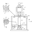
- FIG. 1 depicts a lithographic apparatus according to an embodiment of the invention
- FIGS. 2 and 3 depict a liquid supply system for use in a lithographic projection apparatus
- FIG. 4 depicts another liquid supply system for use in a lithographic projection apparatus
- FIG. 5 depicts a further liquid supply system for use in a lithographic projection apparatus
- FIG. 6 depicts schematically in plan a space of a liquid confinement structure in accordance with an embodiment of the invention.
- FIG. 7 depicts schematically in plan a space of another liquid confinement structure in accordance with an embodiment of the invention.
- FIG. 8 depicts in cross-section a liquid confinement structure and a final element of the projection system according to the invention.
- FIG. 9 depicts in cross-section a final element of the projection system.
- FIG. 10 depicts schematically the final element of FIG. 9 .
- FIG. 1 schematically depicts a lithographic apparatus according to one embodiment of the invention.
- the apparatus comprises:
- the illumination system may include various types of optical components, such as refractive, reflective, magnetic, electromagnetic, electrostatic or other types of optical components, or any combination thereof, for directing, shaping, or controlling radiation.
- optical components such as refractive, reflective, magnetic, electromagnetic, electrostatic or other types of optical components, or any combination thereof, for directing, shaping, or controlling radiation.
- the support structure holds the patterning device in a manner that depends on the orientation of the patterning device, the design of the lithographic apparatus, and other conditions, such as for example whether or not the patterning device is held in a vacuum environment.
- the support structure can use mechanical, vacuum, electrostatic or other clamping techniques to hold the patterning device.
- the support structure may be a frame or a table, for example, which may be fixed or movable as required.
- the support structure may ensure that the patterning device is at a desired position, for example with respect to the projection system. Any use of the terms “reticle” or “mask” herein may be considered synonymous with the more general term “patterning device.”
- patterning device used herein should be broadly interpreted as referring to any device that can be used to impart a radiation beam with a pattern in its cross-section such as to create a pattern in a target portion of the substrate. It should be noted that the pattern imparted to the radiation beam may not exactly correspond to the desired pattern in the target portion of the substrate, for example if the pattern includes phase-shifting features or so called assist features. Generally, the pattern imparted to the radiation beam will correspond to a particular functional layer in a device being created in the target portion, such as an integrated circuit.
- the patterning device may be transmissive or reflective.
- Examples of patterning devices include masks, programmable mirror arrays, and programmable LCD panels.
- Masks are well known in lithography, and include mask types such as binary, alternating phase-shift, and attenuated phase-shift, as well as various hybrid mask types.
- An example of a programmable mirror array employs a matrix arrangement of small mirrors, each of which can be individually tilted so as to reflect an incoming radiation beam in different directions. The tilted mirrors impart a pattern in a radiation beam which is reflected by the mirror matrix.
- projection system used herein should be broadly interpreted as encompassing any type of projection system, including refractive, reflective, catadioptric, magnetic, electromagnetic and electrostatic optical systems, or any combination thereof, as appropriate for the exposure radiation being used, or for other factors such as the use of an immersion liquid or the use of a vacuum. Any use of the term “projection lens” herein may be considered as synonymous with the more general term “projection system”.
- the apparatus is of a transmissive type (e.g. employing a transmissive mask).
- the apparatus may be of a reflective type (e.g. employing a programmable mirror array of a type as referred to above, or employing a reflective mask).
- the lithographic apparatus may be of a type having two (dual stage) or more substrate tables (and/or two or more mask tables). In such “multiple stage” machines the additional tables may be used in parallel, or preparatory steps may be carried out on one or more tables while one or more other tables are being used for exposure.
- the illuminator IL receives a radiation beam from a radiation source SO.
- the source and the lithographic apparatus may be separate entities, for example when the source is an excimer laser. In such cases, the source is not considered to form part of the lithographic apparatus and the radiation beam is passed from the source SO to the illuminator IL with the aid of a beam delivery system BD comprising, for example, suitable directing mirrors and/or a beam expander. In other cases the source may be an integral part of the lithographic apparatus, for example when the source is a mercury lamp.
- the source SO and the illuminator IL, together with the beam delivery system BD if required, may be referred to as a radiation system.
- the illuminator IL may comprise an adjuster AD for adjusting the angular intensity distribution of the radiation beam.
- an adjuster AD for adjusting the angular intensity distribution of the radiation beam.
- the illuminator IL may comprise various other components, such as an integrator IN and a condenser CO.
- the illuminator may be used to condition the radiation beam, to have a desired uniformity and intensity distribution in its cross-section.
- the radiation beam B is incident on the patterning device (e.g., mask MA), which is held on the support structure (e.g., mask table MT), and is patterned by the patterning device. Having traversed the mask MA, the radiation beam B passes through the projection system PS, which focuses the beam onto a target portion C of the substrate W.
- the substrate table WT can be moved accurately, e.g. so as to position different target portions C in the path of the radiation beam B.
- the first positioner PM and another position sensor (which is not explicitly depicted in FIG.
- the mask table MT can be used to accurately position the mask MA with respect to the path of the radiation beam B, e.g. after mechanical retrieval from a mask library, or during a scan.
- movement of the mask table MT may be realized with the aid of a long-stroke module (coarse positioning) and a short-stroke module (fine positioning), which form part of the first positioner PM.
- movement of the substrate table WT may be realized using a long-stroke module and a short-stroke module, which form part of the second positioner PW.
- the mask table MT may be connected to a short-stroke actuator only, or may be fixed.
- Mask MA and substrate W may be aligned using mask alignment marks M 1 , M 2 and substrate alignment marks P 1 , P 2 .
- the substrate alignment marks as illustrated occupy dedicated target portions, they may be located in spaces between target portions (these are known as scribe-lane alignment marks).
- the mask alignment marks may be located between the dies.
- the depicted apparatus could be used in at least one of the following modes:
- step mode the mask table MT and the substrate table WT are kept essentially stationary, while an entire pattern imparted to the radiation beam is projected onto a target portion C at one time (i.e. a single static exposure).
- the substrate table WT is then shifted in the X and/or Y direction so that a different target portion C can be exposed.
- step mode the maximum size of the exposure field limits the size of the target portion C imaged in a single static exposure.
- the mask table MT and the substrate table WT are scanned synchronously while a pattern imparted to the radiation beam is projected onto a target portion C (i.e. a single dynamic exposure).
- the velocity and direction of the substrate table WT relative to the mask table MT may be determined by the (de-)magnification and image reversal characteristics of the projection system PS.
- the maximum size of the exposure field limits the width (in the non-scanning direction) of the target portion in a single dynamic exposure, whereas the length of the scanning motion determines the height (in the scanning direction) of the target portion.
- the mask table MT is kept essentially stationary holding a programmable patterning device, and the substrate table WT is moved or scanned while a pattern imparted to the radiation beam is projected onto a target portion C.
- a pulsed radiation source is employed and the programmable patterning device is updated as required after each movement of the substrate table WT or in between successive radiation pulses during a scan.
- This mode of operation can be readily applied to maskless lithography that utilizes programmable patterning device, such as a programmable mirror array of a type as referred to above.
- FIG. 4 A further immersion lithography solution with a localized liquid supply system is shown in FIG. 4 .
- Liquid is supplied by two groove inlets IN on either side of the projection system PL and is removed by a plurality of discrete outlets OUT arranged radially outwardly of the inlets IN.
- the inlets IN and OUT can be arranged in a plate with a hole in its center and through which the projection beam is projected.
- Liquid is supplied by one groove inlet IN on one side of the projection system PL and removed by a plurality of discrete outlets OUT on the other side of the projection system PL, causing a flow of a thin film of liquid between the projection system PL and the substrate W.
- the choice of which combination of inlet IN and outlets OUT to use can depend on the direction of movement of the substrate W (the other combination of inlet IN and outlets OUT being inactive).
- FIG. 5 Another immersion lithography solution with a localized liquid supply system solution which has been proposed is to provide the liquid supply system with a liquid confinement structure which extends along at least a part of a boundary of the space between the final element of the projection system and the substrate table.
- the liquid confinement structure is substantially stationary relative to the projection system in the XY plane though there may be some relative movement in the Z direction (in the direction of the optical axis).
- a seal is formed between the liquid confinement structure and the surface of the substrate.
- the seal is a contactless seal such as a gas seal.
- the size and shape of the target portion C (which is sometimes referred to as the slit size) can be determined by the illumination optics, such as a quartz rod which is a light mixer and/or a masking unit which is positioned near to the exit of this rod
- Bubbles may be formed in the immersion liquid due to movement of the substrate W and substrate table WT beneath the projection system PL and the substantially stationary liquid confinement system such as that illustrated in FIG. 4 or FIG. 5 .
- Bubbles may be formed in the immersion liquid and thereby reduce the imaging quality of the apparatus
- Liquid confinement systems have been typically designed for use with conventional projection systems PL.
- the last element tends to have a circular cross-section in a plane substantially perpendicular to the optical axis of the projection system (which is the same as a plane substantially parallel to the substrate W).
- the cross-sectional area of the space filled with liquid closely conforms to the shape of the final element of the projection system in one and the same plane. This is designed to be the case to maximize the available space for the liquid supply system which requires many components in a small volume.
- Several different designs of liquid confinement system have been proposed. One or more embodiments of the invention are applicable to all of those different designs including but not limited to those disclosed in U.S. patent publication no.
- FIG. 5 shows a liquid reservoir or space 10 between the projection system and the substrate stage.
- the space 10 is filled with a liquid 11 having a relatively high refractive index, e.g. water, provided via inlet/outlet ducts 13 .
- the liquid has the effect that the radiation of the projection beam has a shorter wavelength in the liquid than in air or a vacuum, allowing smaller features to be resolved.
- the resolution limit of a projection system is determined, inter alia, by the wavelength of the projection beam and the numerical aperture of the system.
- the presence of the liquid may also be regarded as increasing the effective numerical aperture.
- the liquid is effective to increase the depth of field
- a contactless seal to the substrate around the image field of the projection system is formal so that liquid is confined in the space 10 between the substrate surface and the final element of the projection system.
- the space is formed or defined by a liquid confinement structure 12 positioned below and surrounding the final element of the projection system PL. Liquid is brought into the space 10 below the projection system and within the liquid confinement structure 12 .
- the liquid confinement structure 12 extends a little above the final element of the projection system and the liquid level rises above the final element so that a buffer of liquid is provided.
- the liquid confinement structure 12 has an inner periphery that at the upper end, in an embodiment, closely conforms to the step of the projection system or the final element thereof and may, e.g., be round
- the liquid is confined in the space 10 by a gas seal 16 between the bottom of the liquid confinement structure 12 and the surface of the substrate W.
- the gas seal is formed by gas, e.g. air, synthetic air, N 2 or an inert gas, provided under pressure via inlet 15 to the gap between liquid confinement structure 12 and substrate and extracted via first outlet 14 .
- gas e.g. air, synthetic air, N 2 or an inert gas
- the overpressure on the gas inlet 15 , vacuum level on the first outlet 14 and geometry of the gap are arranged so that there is a high-velocity gas flow inwards that confines the liquid
- liquid confinement structure 12 may be used.
- the gas seal may be replaced by a combination of a single phase extractor, a recess and a gas knife as is described in U.S. patent application Ser. No. 11/098,615, filed 5 Apr. 2005, hereby incorporated in its entirety by reference herein.
- a gas seal may be replaced by a hydrostatic or hydrodynamic bearing as is described in U.S. patent application publication no. US 2005-018155, each of which are hereby incorporated in their entirety by reference
- the cross-section of the space 10 in a plane parallel to the top surface of the substrate W at a position closest to the substrate is fashioned to conform closely to the shape of the target portion TP (sometimes referred to as the illumination slit area).
- the target portion TP sometimes referred to as the illumination slit area.
- FIG. 6 which is an illustration of the liquid confinement structure 12 in plan, the space 10 is defined by walls 20 extending between a lower opening 40 of the space 10 in the lower surface of the liquid confinement structure 12 and an upper opening 60 in the upper surface of the liquid confinement structure 12 .
- the upper opening 60 is circular such that the liquid confinement structure 12 may be used with a conventional projection system PL in which the final element of the projection system is radially symmetric and the bottom opening 40 which is closest to the substrate W is rectangular and conforms in shape closely to the shape of the target portion TP. Furthermore, the lower opening 40 also closely conforms in size to that of the target portion TP though of course it cannot be smaller than the target portion TP.
- the area of the lower opening 40 or of the cross-section of the space in a plane substantially parallel to the substrate W at a position closest to the substrate W is less than 1.5 times the area of the target portion TP, in an embodiment less than 1.4, 1.3, 1.2 or 1.1 times the area of the target portion TP. This difference is to account for relative movement of the liquid supply system to the final element either in the case of ‘play’ or so that the movement can be deliberately carried out
- the surface 20 of the liquid confinement structure 12 which defines the space 10 in which the liquid is confined is shaped to transfer smoothly from the shape of the upper opening 60 to the lower opening 40 and accommodates the shape of the final element of the projection system and allows some relative movement of the confinement system as is described in European patent application publication no. EP 1477856, the contents of which is hereby incorporated in its entirety by reference.
- EP 1477856 the contents of which is hereby incorporated in its entirety by reference.
- the shapes of the upper and lower openings, 40 , 60 are similar, at least both rectilinear. This is particularly easy to arrange for if the projection system is close to the substrate.
- FIG. 7 A rectilinear situation is illustrated in which the upper opening 60 is square and the lower opening 40 is rectangular. In this arrangement, it should be easy to achieve parallel flow of immersion liquid across the target portion TP without re-circulation of immersion liquid. Re-circulation of immersion liquid is to be avoided because re-circulated immersion liquid may be heated up by the projection beam PB more than non-re-circulated immersion liquid and the variation in temperature can lead to variations in refractive index of the immersion liquid in the space
- the size of the lower opening 40 of the space in the liquid confinement structure 12 is reduced or minimized as is illustrated in FIGS. 6 and 7 by making its cross-sectional shape and/or size conform closely or be similar to that of the target portion TP, during scanning of a whole substrate W the number of scans in which the opening 40 passes over an edge of the substrate is greatly reduced.
- the opportunity for bubble formation in the immersion liquid in the space 10 due to passing over of the edge of the substrate is reduced and so is the area from which immersion liquid can evaporate
- FIGS. 8-10 illustrate an embodiment of the invention in which both the final element of the projection system and the liquid confinement structure 12 are optimized in shape and geometry so that the size of the lower opening 40 can be made to closely conform to the shape and/or size of the target portion TP without deleteriously affecting other operating conditions such as the ability to generate parallel flow of immersion liquid across the target portion TP or reducing the available volume for the liquid supply system.
- this embodiment may increase available volume for the liquid supply system over prior systems
- a liquid confinement structure 12 similar to that illustrated in FIG. 7 is used.
- the lower opening 40 of the space is of a similar shape and dimension to the target portion TP in a plane PL 2 which is substantially parallel to the substrate W and adjacent the substrate W, e.g., at a position closest to the substrate W.
- the liquid confinement structure 12 partly surrounds the final element of the projection system PL.
- a plane PL 1 exists which is substantially parallel to the plane of the top surface of the substrate W and also intersects both the space 10 defined by the liquid confinement structure 12 and the lower end of the final element of the projection system PL.
- the cross-sectional shape and size of the space is similar to that of the cross-sectional shape and size of the final element of the projection system PL.
- the final element of the projection system PL is shaped such that it also has a rectangular or square cross-section in that plane so that it is possible for the inner surface of the liquid confinement structure 12 which defines the space to transfer in shape from the lower opening 40 to the upper opening 60 without needing to convert straight lines to curved lines. This helps in the establishment of parallel flow of immersion liquid across the target portion TP and simplifies the shaping of walls 20 .
- the walls 20 are all substantially flat.
- the shape of the lower opening and upper opening, and thereby the shape of the cross-section of the final element of the projection system PL are similar to the shape of the target portion
- a space 10 is illustrated which has a cross-section in a plane substantially parallel to the substrate W which decreases as the substrate W is approached. This need not necessarily be the case and it may be that the upper and lower openings 40 , 60 are the same or substantially the same size so that the side walls of the space defined by the liquid confinement structure 12 are parallel in cross-section.
- the rate of increase/decrease in cross-sectional area as the substrate W is left/approached is not necessarily constant and a space 10 with two gradients of inner side wall 20 is provided, a steep gradient between the substrate 20 and substantially the bottom of the projection system and another shallower gradient above that
- FIG. 9 illustrates a final element of the projection system.
- the dotted lines show the shape of a typical final element of a projection system and it can be seen that those parts of the final element can be removed without affecting the optical properties of the final element in use. Machining away the areas shown in dotted lines is one way of manufacturing such an element.
- the bottom surface of the final element is a shape to which the space of the liquid confinement structure 12 can be closely formed without the need to use a curved upper opening 60 .
- the very bottom of the final element is illustrated as having a coating 100 applied to it (or a quartz plate or so-called abslussplatte 100 ).
- the coating or quartz plate 100 is shown as being flat. However, this need not be the case and the very bottom surface of the final element may be curved and may or may not have a coating or quartz plate applied to it
- FIG. 10 is a three dimensional illustration of the final element of the projection system in which the transition from a curved upper surface to a non-curved lower surface is clearly seen.
- the top half of the element is normally shaped and it is the bottom half of the element which has flat sides joined by straight edges 70 i.e. has a rectilinear cross-sectional shape in a plane substantially parallel to the substrate W
- a lithographic apparatus comprising: a substrate table constructed to hold a substrate; and a projection system configured to project a patterned radiation beam onto a target portion of the substrate and having an element immediately adjacent the substrate, the element having a cross-sectional shape in a plane substantially parallel to the substrate which is rectilinear.
- the cross-sectional shape is similar to the shape of the target portion.
- a bottom surface closest to the substrate of the element is curved.
- the target portion is substantially rectangular.
- the cross-sectional shape of the element in a plane substantially parallel to the substrate has an area which is less than 1.5 times the area of the target portion.
- the apparatus further comprises a liquid confinement structure having a surface at least in part defining a space configured to contain a liquid between the projection system and the substrate, wherein in a plane substantially parallel to the substrate the space has a cross-section which substantially conforms in shape to the shape of the target portion.
- the cross-section of the space has an area which is less than 1.5 times the area of the target portion.
- the surface of the liquid confinement structure extends beyond a bottom surface closest to the substrate of the element, and, in a plane which intersects both the space and the element and which is substantially parallel to the substrate, the cross-sectional shapes and areas of the space and element closely conform.
- a lithographic apparatus comprising: a substrate table constructed to hold a substrate; a projection system configured to project a patterned radiation beam onto a target portion of the substrate; and a liquid confinement structure having a surface at least in part defining a space configured to contain liquid between the projection system and the substrate, wherein in a plane substantially parallel to the substrate, at a position closest to the substrate, the space has a cross-section which substantially conforms in shape, area, or both to that of the target portion.
- the space is tapered such that the cross-sectional area of the space in a plane substantially parallel to the substrate reduces as the substrate is approached.
- the cross-sectional shape of the space in a plane substantially parallel to the substrate changes from a position furthest from the substrate to a position closest to the substrate, wherein at the position closest to the substrate the cross-sectional shape is substantially the same as the shape of the target portion.
- a device manufacturing method comprising using a projection system to project on a target portion of a substrate a patterned beam of radiation, wherein an element of the projection system immediately adjacent the substrate has a cross-sectional shape in a plane substantially parallel to the substrate which is rectilinear.
- a device manufacturing method comprising using a projection system to project on a target portion of a substrate a patterned beam of radiation, wherein a liquid is provided in a space between the projection system and the substrate and which space is defined at least in part by a surface of a liquid confinement structure and the space, an element of the projection system immediately adjacent the substrate, or both, has a cross-section in a plane substantially parallel to the substrate which conforms closely in size, shape, or both to that of the target portion.
- lithographic apparatus in the manufacture of ICs
- the lithographic apparatus described herein may have other applications, such as the manufacture of integrated optical systems, guidance and detection patterns for magnetic domain memories, flat-panel displays, liquid-crystal displays (LCDs), thin-film magnetic heads, etc.
- LCDs liquid-crystal displays
- any use of the terms “wafer” or “die” herein may be considered as synonymous with the more general terms “substrate” or “target portion”, respectively.
- the substrate referred to herein may be processed, before or after exposure, in for example a track (a tool that typically applies a layer of resist to a substrate and develops the exposed resist), a metrology tool and/or an inspection tool. Where applicable, the disclosure herein may be applied to such and other substrate processing tools. Further, the substrate may be processed more than once, for example in order to create a multi-layer IC, so that the term substrate used herein may also refer to a substrate that already contains multiple processed layers.
- imprint lithography a topography in a patterning device defines the pattern created on a substrate.
- the topography of the patterning device may be pressed into a layer of resist supplied to the substrate whereupon the resist is cured by applying electromagnetic radiation, heat, pressure or a combination thereof.
- the patterning device is moved out of the resist leaving a pattern in it after the resist is cured.
- a liquid supply system as contemplated herein should be broadly construed. In certain embodiments, it may be a mechanism or combination of structures that provides a liquid to a space between the projection system and the substrate and/or substrate table. It may comprise a combination of one or more structures, one or more liquid inlets, one or more gas inlets, one or more gas outlets, and/or one or more liquid outlets that provide liquid to the space.
- a surface of the space may be a portion of the substrate and/or substrate table, or a surface of the space may completely cover a surface of the substrate and/or substrate table, or the space may envelop the substrate and/or substrate table.
- the liquid supply system may optionally further include one or more elements to control the position, quantity, quality, shape, flow rate or any other features of the liquid.
Abstract
Description
-
- an illumination system (illuminator) IL configured to condition a radiation beam B (e.g. UV radiation or DUV radiation).
- a support structure (e.g. a mask table) MT constructed to support a patterning device (e.g. a mask) MA and connected to a first positioner PM configured to accurately position the patterning device in accordance with certain parameters;
- a substrate table (e.g. a wafer table) WT constructed to hold a substrate (e.g. a resist-coated wafer) W and connected to a second positioner PW configured to accurately position the substrate in accordance with certain parameters; and
- a projection system (e.g. a refractive projection lens system) PS configured to project a pattern imparted to the radiation beam B by patterning device MA onto a target portion C (e.g. comprising one or more dies) of the substrate W.
Claims (20)
Priority Applications (4)
| Application Number | Priority Date | Filing Date | Title |
|---|---|---|---|
| US13/589,841 US8860924B2 (en) | 2005-05-03 | 2012-08-20 | Lithographic apparatus and device manufacturing method |
| US14/484,076 US9477153B2 (en) | 2005-05-03 | 2014-09-11 | Lithographic apparatus and device manufacturing method |
| US14/871,795 US10451973B2 (en) | 2005-05-03 | 2015-09-30 | Lithographic apparatus and device manufacturing method |
| US15/482,587 US10488759B2 (en) | 2005-05-03 | 2017-04-07 | Lithographic apparatus and device manufacturing method |
Applications Claiming Priority (2)
| Application Number | Priority Date | Filing Date | Title |
|---|---|---|---|
| US11/120,186 US8248577B2 (en) | 2005-05-03 | 2005-05-03 | Lithographic apparatus and device manufacturing method |
| US13/589,841 US8860924B2 (en) | 2005-05-03 | 2012-08-20 | Lithographic apparatus and device manufacturing method |
Related Parent Applications (1)
| Application Number | Title | Priority Date | Filing Date |
|---|---|---|---|
| US11/120,186 Continuation US8248577B2 (en) | 2005-05-03 | 2005-05-03 | Lithographic apparatus and device manufacturing method |
Related Child Applications (1)
| Application Number | Title | Priority Date | Filing Date |
|---|---|---|---|
| US14/484,076 Continuation US9477153B2 (en) | 2005-05-03 | 2014-09-11 | Lithographic apparatus and device manufacturing method |
Publications (2)
| Publication Number | Publication Date |
|---|---|
| US20130070219A1 US20130070219A1 (en) | 2013-03-21 |
| US8860924B2 true US8860924B2 (en) | 2014-10-14 |
Family
ID=36754253
Family Applications (5)
| Application Number | Title | Priority Date | Filing Date |
|---|---|---|---|
| US11/120,186 Active 2026-03-03 US8248577B2 (en) | 2005-05-03 | 2005-05-03 | Lithographic apparatus and device manufacturing method |
| US13/589,841 Expired - Fee Related US8860924B2 (en) | 2005-05-03 | 2012-08-20 | Lithographic apparatus and device manufacturing method |
| US14/484,076 Active US9477153B2 (en) | 2005-05-03 | 2014-09-11 | Lithographic apparatus and device manufacturing method |
| US14/871,795 Expired - Fee Related US10451973B2 (en) | 2005-05-03 | 2015-09-30 | Lithographic apparatus and device manufacturing method |
| US15/482,587 Expired - Fee Related US10488759B2 (en) | 2005-05-03 | 2017-04-07 | Lithographic apparatus and device manufacturing method |
Family Applications Before (1)
| Application Number | Title | Priority Date | Filing Date |
|---|---|---|---|
| US11/120,186 Active 2026-03-03 US8248577B2 (en) | 2005-05-03 | 2005-05-03 | Lithographic apparatus and device manufacturing method |
Family Applications After (3)
| Application Number | Title | Priority Date | Filing Date |
|---|---|---|---|
| US14/484,076 Active US9477153B2 (en) | 2005-05-03 | 2014-09-11 | Lithographic apparatus and device manufacturing method |
| US14/871,795 Expired - Fee Related US10451973B2 (en) | 2005-05-03 | 2015-09-30 | Lithographic apparatus and device manufacturing method |
| US15/482,587 Expired - Fee Related US10488759B2 (en) | 2005-05-03 | 2017-04-07 | Lithographic apparatus and device manufacturing method |
Country Status (8)
| Country | Link |
|---|---|
| US (5) | US8248577B2 (en) |
| EP (2) | EP1837705A3 (en) |
| JP (2) | JP4749933B2 (en) |
| KR (1) | KR100768945B1 (en) |
| CN (2) | CN1858657B (en) |
| DE (1) | DE602006009174D1 (en) |
| SG (2) | SG126922A1 (en) |
| TW (2) | TW201104371A (en) |
Cited By (1)
| Publication number | Priority date | Publication date | Assignee | Title |
|---|---|---|---|---|
| US10488759B2 (en) | 2005-05-03 | 2019-11-26 | Asml Netherlands B.V. | Lithographic apparatus and device manufacturing method |
Families Citing this family (6)
| Publication number | Priority date | Publication date | Assignee | Title |
|---|---|---|---|---|
| US7324185B2 (en) | 2005-03-04 | 2008-01-29 | Asml Netherlands B.V. | Lithographic apparatus and device manufacturing method |
| KR101524964B1 (en) | 2005-05-12 | 2015-06-01 | 가부시키가이샤 니콘 | Projection optical system, exposure apparatus and exposure method |
| EP2131241B1 (en) * | 2008-05-08 | 2019-07-31 | ASML Netherlands B.V. | Fluid handling structure, lithographic apparatus and device manufacturing method |
| US9385089B2 (en) | 2013-01-30 | 2016-07-05 | Seagate Technology Llc | Alignment mark recovery with reduced topography |
| US9343089B2 (en) * | 2013-03-08 | 2016-05-17 | Seagate Technology Llc | Nanoimprint lithography for thin film heads |
| CN104950586B (en) * | 2014-03-25 | 2017-06-06 | 上海微电子装备有限公司 | A kind of immersion liquid limiting mechanism |
Citations (110)
| Publication number | Priority date | Publication date | Assignee | Title |
|---|---|---|---|---|
| US3573975A (en) | 1968-07-10 | 1971-04-06 | Ibm | Photochemical fabrication process |
| US3648587A (en) | 1967-10-20 | 1972-03-14 | Eastman Kodak Co | Focus control for optical instruments |
| EP0023231A1 (en) | 1979-07-27 | 1981-02-04 | Tabarelli, Werner, Dr. | Optical lithographic method and apparatus for copying a pattern onto a semiconductor wafer |
| FR2474708A1 (en) | 1980-01-24 | 1981-07-31 | Dme | Micro:photo:lithographic process giving high line resolution - with application of immersion oil between mask and photosensitive layer before exposure |
| US4346164A (en) | 1980-10-06 | 1982-08-24 | Werner Tabarelli | Photolithographic method for the manufacture of integrated circuits |
| US4390273A (en) | 1981-02-17 | 1983-06-28 | Censor Patent-Und Versuchsanstalt | Projection mask as well as a method and apparatus for the embedding thereof and projection printing system |
| US4396705A (en) | 1980-09-19 | 1983-08-02 | Hitachi, Ltd. | Pattern forming method and pattern forming apparatus using exposures in a liquid |
| US4405701A (en) | 1981-07-29 | 1983-09-20 | Western Electric Co. | Methods of fabricating a photomask |
| JPS58202448A (en) | 1982-05-21 | 1983-11-25 | Hitachi Ltd | Exposing device |
| DD206607A1 (en) | 1982-06-16 | 1984-02-01 | Mikroelektronik Zt Forsch Tech | METHOD AND DEVICE FOR ELIMINATING INTERFERENCE EFFECTS |
| US4480910A (en) | 1981-03-18 | 1984-11-06 | Hitachi, Ltd. | Pattern forming apparatus |
| US4509852A (en) | 1980-10-06 | 1985-04-09 | Werner Tabarelli | Apparatus for the photolithographic manufacture of integrated circuit elements |
| DD221563A1 (en) | 1983-09-14 | 1985-04-24 | Mikroelektronik Zt Forsch Tech | IMMERSIONS OBJECTIVE FOR THE STEP-BY-STEP PROJECTION IMAGING OF A MASK STRUCTURE |
| DD224448A1 (en) | 1984-03-01 | 1985-07-03 | Zeiss Jena Veb Carl | DEVICE FOR PHOTOLITHOGRAPHIC STRUCTURAL TRANSMISSION |
| DD242880A1 (en) | 1983-01-31 | 1987-02-11 | Kuch Karl Heinz | DEVICE FOR PHOTOLITHOGRAPHIC STRUCTURAL TRANSMISSION |
| JPS6265326A (en) | 1985-09-18 | 1987-03-24 | Hitachi Ltd | Exposure device |
| JPS62121417A (en) | 1985-11-22 | 1987-06-02 | Hitachi Ltd | Liquid-immersion objective lens device |
| JPS63157419A (en) | 1986-12-22 | 1988-06-30 | Toshiba Corp | Fine pattern transfer apparatus |
| EP0418427A2 (en) | 1989-09-06 | 1991-03-27 | Eiichi Miyake | Exposure process |
| US5040020A (en) | 1988-03-31 | 1991-08-13 | Cornell Research Foundation, Inc. | Self-aligned, high resolution resonant dielectric lithography |
| JPH04305917A (en) | 1991-04-02 | 1992-10-28 | Nikon Corp | Adhesion type exposure device |
| JPH04305915A (en) | 1991-04-02 | 1992-10-28 | Nikon Corp | Adhesion type exposure device |
| US5298939A (en) | 1991-11-04 | 1994-03-29 | Swanson Paul A | Method and apparatus for transfer of a reticle pattern onto a substrate by scanning |
| JPH06124873A (en) | 1992-10-09 | 1994-05-06 | Canon Inc | Liquid-soaking type projection exposure apparatus |
| JPH07132262A (en) | 1992-12-21 | 1995-05-23 | Tokyo Electron Ltd | Liquid treating device of immersion type |
| JPH07220990A (en) | 1994-01-28 | 1995-08-18 | Hitachi Ltd | Pattern forming method and exposure apparatus therefor |
| US5610683A (en) | 1992-11-27 | 1997-03-11 | Canon Kabushiki Kaisha | Immersion type projection exposure apparatus |
| JPH10228661A (en) | 1997-02-14 | 1998-08-25 | Sony Corp | Master disk manufacturing aligner for optical recording medium |
| JPH10255319A (en) | 1997-03-12 | 1998-09-25 | Hitachi Maxell Ltd | Master disk exposure device and method therefor |
| US5825043A (en) | 1996-10-07 | 1998-10-20 | Nikon Precision Inc. | Focusing and tilting adjustment system for lithography aligner, manufacturing apparatus or inspection apparatus |
| JPH10303114A (en) | 1997-04-23 | 1998-11-13 | Nikon Corp | Immersion aligner |
| JPH10340846A (en) | 1997-06-10 | 1998-12-22 | Nikon Corp | Aligner, its manufacture, exposing method and device manufacturing method |
| US5900354A (en) | 1997-07-03 | 1999-05-04 | Batchelder; John Samuel | Method for optical inspection and lithography |
| JPH11176727A (en) | 1997-12-11 | 1999-07-02 | Nikon Corp | Projection aligner |
| WO1999049504A1 (en) | 1998-03-26 | 1999-09-30 | Nikon Corporation | Projection exposure method and system |
| JP2000058436A (en) | 1998-08-11 | 2000-02-25 | Nikon Corp | Projection aligner and exposure method |
| EP1039511A1 (en) | 1997-12-12 | 2000-09-27 | Nikon Corporation | Projection exposure method and projection aligner |
| JP2001091849A (en) | 1999-09-21 | 2001-04-06 | Olympus Optical Co Ltd | Liquid immersion objective lens for microscope |
| US6236634B1 (en) | 1996-08-26 | 2001-05-22 | Digital Papyrus Corporation | Method and apparatus for coupling an optical lens to a disk through a coupling medium having a relatively high index of refraction |
| US20020020821A1 (en) | 2000-08-08 | 2002-02-21 | Koninklijke Philips Electronics N.V. | Method of manufacturing an optically scannable information carrier |
| US20020163629A1 (en) | 2001-05-07 | 2002-11-07 | Michael Switkes | Methods and apparatus employing an index matching medium |
| US20030123040A1 (en) | 2001-11-07 | 2003-07-03 | Gilad Almogy | Optical spot grid array printer |
| US6600547B2 (en) | 2001-09-24 | 2003-07-29 | Nikon Corporation | Sliding seal |
| US6603130B1 (en) | 1999-04-19 | 2003-08-05 | Asml Netherlands B.V. | Gas bearings for use with vacuum chambers and their application in lithographic projection apparatuses |
| US20040000627A1 (en) | 2002-06-28 | 2004-01-01 | Carl Zeiss Semiconductor Manufacturing Technologies Ag | Method for focus detection and an imaging system with a focus-detection system |
| US20040075895A1 (en) | 2002-10-22 | 2004-04-22 | Taiwan Semiconductor Manufacturing Co., Ltd. | Apparatus for method for immersion lithography |
| US20040114117A1 (en) | 2002-11-18 | 2004-06-17 | Asml Netherlands B.V. | Lithographic apparatus and device manufacturing method |
| WO2004053957A1 (en) | 2002-12-10 | 2004-06-24 | Nikon Corporation | Surface position detection apparatus, exposure method, and device porducing method |
| WO2004053959A1 (en) | 2002-12-10 | 2004-06-24 | Nikon Corporation | Optical device and projection exposure apparatus using such optical device |
| WO2004053952A1 (en) | 2002-12-10 | 2004-06-24 | Nikon Corporation | Exposure apparatus and method for manufacturing device |
| WO2004053955A1 (en) | 2002-12-10 | 2004-06-24 | Nikon Corporation | Exposure system and device producing method |
| WO2004053958A1 (en) | 2002-12-10 | 2004-06-24 | Nikon Corporation | Exposure apparatus and method for manufacturing device |
| WO2004053951A1 (en) | 2002-12-10 | 2004-06-24 | Nikon Corporation | Exposure method, exposure apparatus and method for manufacturing device |
| WO2004053954A1 (en) | 2002-12-10 | 2004-06-24 | Nikon Corporation | Exposure apparatus and method for manufacturing device |
| WO2004053950A1 (en) | 2002-12-10 | 2004-06-24 | Nikon Corporation | Exposure apparatus and method for manufacturing device |
| WO2004053953A1 (en) | 2002-12-10 | 2004-06-24 | Nikon Corporation | Exposure apparatus and method for manufacturing device |
| WO2004053596A2 (en) | 2002-12-10 | 2004-06-24 | Carl Zeiss Smt Ag | Method for adjusting a desired optical property of a positioning lens and microlithographic projection exposure system |
| WO2004053956A1 (en) | 2002-12-10 | 2004-06-24 | Nikon Corporation | Exposure apparatus, exposure method and method for manufacturing device |
| US20040125351A1 (en) | 2002-12-30 | 2004-07-01 | Krautschik Christof Gabriel | Immersion lithography |
| WO2004055803A1 (en) | 2002-12-13 | 2004-07-01 | Koninklijke Philips Electronics N.V. | Liquid removal in a method and device for irradiating spots on a layer |
| WO2004057589A1 (en) | 2002-12-19 | 2004-07-08 | Koninklijke Philips Electronics N.V. | Method and device for irradiating spots on a layer |
| WO2004057590A1 (en) | 2002-12-19 | 2004-07-08 | Koninklijke Philips Electronics N.V. | Method and device for irradiating spots on a layer |
| JP2004193252A (en) | 2002-12-10 | 2004-07-08 | Nikon Corp | Exposing method and device manufacturing method |
| US20040136494A1 (en) | 2002-11-12 | 2004-07-15 | Asml Netherlands B.V. | Lithographic apparatus and device manufacturing method |
| US20040160582A1 (en) | 2002-11-12 | 2004-08-19 | Asml Netherlands B.V. | Lithographic apparatus and device manufacturing method |
| US20040165159A1 (en) | 2002-11-12 | 2004-08-26 | Asml Netherlands B.V. | Lithographic apparatus and device manufacturing method |
| US20040207824A1 (en) | 2002-11-12 | 2004-10-21 | Asml Netherlands B.V. | Lithographic apparatus and device manufacturing method |
| US20040211920A1 (en) | 2002-11-12 | 2004-10-28 | Asml Netherlands B.V. | Lithographic apparatus and device manufacturing method |
| US20040239954A1 (en) | 2003-05-28 | 2004-12-02 | Joerg Bischoff | Resolution enhanced optical metrology |
| WO2004095135A3 (en) | 2003-04-17 | 2004-12-09 | Nippon Kogaku Kk | Optical arrangement of autofocus elements for use with immersion lithography |
| US20040263809A1 (en) | 2003-06-27 | 2004-12-30 | Canon Kabushiki Kaisha | Immersion exposure technique |
| US20050007569A1 (en) | 2003-05-13 | 2005-01-13 | Asml Netherlands B.V. | Lithographic apparatus and device manufacturing method |
| US20050018155A1 (en) | 2003-06-27 | 2005-01-27 | Asml Netherlands B. V. | Lithographic apparatus and device manufacturing method |
| US20050024609A1 (en) | 2003-06-11 | 2005-02-03 | Asml Netherlands B.V. | Lithographic apparatus and device manufacturing method |
| US20050030497A1 (en) | 2003-06-25 | 2005-02-10 | Takashi Nakamura | Liquid immersion type exposure apparatus |
| WO2004093160A3 (en) | 2003-04-10 | 2005-02-24 | Nippon Kogaku Kk | Run-off path to collect liquid for an immersion lithography apparatus |
| US20050046813A1 (en) | 2003-07-16 | 2005-03-03 | Asmil Netherlands B.V. | Lithographic apparatus and device manufacturing method |
| WO2005020298A1 (en) | 2003-08-26 | 2005-03-03 | Nikon Corporation | Optical element and exposure device |
| US20050046934A1 (en) | 2003-08-29 | 2005-03-03 | Tokyo Electron Limited | Method and system for drying a substrate |
| US20050052632A1 (en) | 2003-09-09 | 2005-03-10 | Canon Kabushiki Kaisha | Exposure technique |
| WO2004093159A3 (en) | 2003-04-09 | 2005-03-17 | Nippon Kogaku Kk | Immersion lithography fluid control system |
| EP1519230A1 (en) | 2003-09-29 | 2005-03-30 | ASML Netherlands B.V. | Lithographic apparatus and device manufacturing method |
| US20050068639A1 (en) | 2003-09-26 | 2005-03-31 | Fortis Systems Inc. | Contact printing using a magnified mask image |
| JP2005093997A (en) | 2003-08-29 | 2005-04-07 | Asml Netherlands Bv | Lithographic apparatus and manufacturing method of device |
| EP1524558A1 (en) | 2003-10-15 | 2005-04-20 | ASML Netherlands B.V. | Lithographic apparatus and device manufacturing method |
| WO2004090577A3 (en) | 2003-04-11 | 2005-04-21 | Nippon Kogaku Kk | Maintaining immersion fluid under a lithographic projection lens |
| US20050094125A1 (en) | 2003-10-31 | 2005-05-05 | Nikon Corporation | Supporting plate, stage device, exposure apparatus, and exposure method |
| WO2004090633A3 (en) | 2003-04-10 | 2005-05-12 | Nippon Kogaku Kk | An electro-osmotic element for an immersion lithography apparatus |
| WO2005034174A3 (en) | 2003-10-03 | 2005-06-09 | Micronic Laser Systems Ab | Method and device for immersion lithography |
| US20050122505A1 (en) | 2003-12-08 | 2005-06-09 | Canon Kabushiki Kaisha | Substrate-holding technique |
| WO2004092830A3 (en) | 2003-04-11 | 2005-06-16 | Nippon Kogaku Kk | Liquid jet and recovery system for immersion lithography |
| US20050132914A1 (en) | 2003-12-23 | 2005-06-23 | Asml Netherlands B.V. | Lithographic apparatus, alignment apparatus, device manufacturing method, and a method of converting an apparatus |
| US20050134817A1 (en) | 2003-06-25 | 2005-06-23 | Takashi Nakamura | Liquid immersion type exposure apparatus |
| US20050140948A1 (en) | 2003-12-26 | 2005-06-30 | Canon Kabushiki Kaisha | Exposure apparatus and method |
| US20050146694A1 (en) | 2004-01-07 | 2005-07-07 | Toshinobu Tokita | Exposure apparatus and device manufacturing method |
| US20050146693A1 (en) | 2003-12-09 | 2005-07-07 | Yoshinori Ohsaki | Exposure apparatus |
| US20050151942A1 (en) | 2003-12-26 | 2005-07-14 | Canon Kabushiki Kaisha | Exposure method and apparatus |
| US20050200815A1 (en) | 2004-02-09 | 2005-09-15 | Canon Kabushiki Kaisha | Projection exposure apparatus, device manufacturing method, and sensor unit |
| WO2005010611A3 (en) | 2003-07-08 | 2005-09-15 | Nippon Kogaku Kk | Wafer table for immersion lithography |
| WO2005024517A3 (en) | 2003-09-03 | 2005-09-29 | Nikon Res Corp Of America | Apparatus and method for providing fluid for immersion lithography |
| US20050213066A1 (en) * | 2004-03-29 | 2005-09-29 | Yuhei Sumiyoshi | Exposure apparatus |
| US20050213065A1 (en) | 2004-03-29 | 2005-09-29 | Atsushi Kitaoka | Exposure apparatus and method |
| US20050219489A1 (en) | 2002-12-10 | 2005-10-06 | Nikon Corporation | Exposure apparatus and method for producing device |
| US20050233081A1 (en) | 2003-09-04 | 2005-10-20 | Toshinobu Tokita | Liquid immersion type exposure apparatus |
| WO2004093130A3 (en) | 2003-04-11 | 2005-11-03 | Nippon Kogaku Kk | Cleanup method for optics in immersion lithography |
| WO2004092833A3 (en) | 2003-04-10 | 2005-12-01 | Nippon Kogaku Kk | Environmental system including a transport region for an immersion lithography apparatus |
| US20060244938A1 (en) | 2004-05-04 | 2006-11-02 | Karl-Heinz Schuster | Microlitographic projection exposure apparatus and immersion liquid therefore |
| WO2004090634A3 (en) | 2003-04-10 | 2007-03-01 | Nippon Kogaku Kk | Environmental system including vaccum scavange for an immersion lithography apparatus |
| US7411653B2 (en) * | 2003-10-28 | 2008-08-12 | Asml Netherlands B.V. | Lithographic apparatus |
| US8248577B2 (en) * | 2005-05-03 | 2012-08-21 | Asml Netherlands B.V. | Lithographic apparatus and device manufacturing method |
Family Cites Families (160)
| Publication number | Priority date | Publication date | Assignee | Title |
|---|---|---|---|---|
| DE242880C (en) | ||||
| DE206607C (en) | ||||
| DE221563C (en) | ||||
| DE224448C (en) | ||||
| US1954755A (en) | 1931-12-05 | 1934-04-10 | Firm Ernst Leitz | Microscope |
| GB669921A (en) | 1949-05-26 | 1952-04-09 | D & P Studios Ltd | Improvements in and relating to optical projection apparatus |
| JPS5919912A (en) | 1982-07-26 | 1984-02-01 | Hitachi Ltd | Immersion distance holding device |
| JPS6187125A (en) | 1984-09-20 | 1986-05-02 | Canon Inc | Projecting device for exposing slit |
| JPS62121417U (en) | 1986-01-24 | 1987-08-01 | ||
| US4747678A (en) | 1986-12-17 | 1988-05-31 | The Perkin-Elmer Corporation | Optical relay system with magnification |
| JPS63157419U (en) | 1987-03-31 | 1988-10-14 | ||
| US4953960A (en) | 1988-07-15 | 1990-09-04 | Williamson David M | Optical reduction system |
| JPH04130710A (en) | 1990-09-21 | 1992-05-01 | Hitachi Ltd | Apparatus for exposure of light |
| JPH04133414A (en) | 1990-09-26 | 1992-05-07 | Nec Yamaguchi Ltd | Reduced projection and aligner |
| JP3084760B2 (en) | 1991-02-28 | 2000-09-04 | 株式会社ニコン | Exposure method and exposure apparatus |
| US5121256A (en) | 1991-03-14 | 1992-06-09 | The Board Of Trustees Of The Leland Stanford Junior University | Lithography system employing a solid immersion lens |
| JPH04211110A (en) | 1991-03-20 | 1992-08-03 | Hitachi Ltd | Projection aligner and aligning method |
| JPH0545886A (en) | 1991-08-12 | 1993-02-26 | Nikon Corp | Exposure device for square substrate |
| US5212593A (en) | 1992-02-06 | 1993-05-18 | Svg Lithography Systems, Inc. | Broad band optical reduction system using matched multiple refractive element materials |
| DE4344908A1 (en) | 1993-01-08 | 1994-07-14 | Nikon Corp | Condensing lens system for specimen examination by reflex microscope |
| US5537260A (en) | 1993-01-26 | 1996-07-16 | Svg Lithography Systems, Inc. | Catadioptric optical reduction system with high numerical aperture |
| JP3747958B2 (en) | 1995-04-07 | 2006-02-22 | 株式会社ニコン | Catadioptric optics |
| JPH07122469A (en) | 1993-10-20 | 1995-05-12 | Nikon Corp | Projection aligner |
| JP3339144B2 (en) | 1993-11-11 | 2002-10-28 | 株式会社ニコン | Scanning exposure apparatus and exposure method |
| JPH0982626A (en) | 1995-09-12 | 1997-03-28 | Nikon Corp | Projection exposure device |
| DE19535392A1 (en) | 1995-09-23 | 1997-03-27 | Zeiss Carl Fa | Radial polarization-rotating optical arrangement and microlithography projection exposure system with it |
| US6270696B1 (en) | 1996-06-03 | 2001-08-07 | Terastor Corporation | Method of fabricating and integrating an optical assembly into a flying head |
| JPH103039A (en) | 1996-06-14 | 1998-01-06 | Nikon Corp | Reflective/refractive optical system |
| JPH1020195A (en) | 1996-06-28 | 1998-01-23 | Nikon Corp | Cata-dioptric system |
| JPH1055713A (en) | 1996-08-08 | 1998-02-24 | Ushio Inc | Ultraviolet irradiation device |
| JPH1092735A (en) | 1996-09-13 | 1998-04-10 | Nikon Corp | Aligner |
| JP2914315B2 (en) | 1996-09-20 | 1999-06-28 | 日本電気株式会社 | Scanning reduction projection exposure apparatus and distortion measuring method |
| JP3991166B2 (en) | 1996-10-25 | 2007-10-17 | 株式会社ニコン | Illumination optical apparatus and exposure apparatus provided with the illumination optical apparatus |
| JPH11283903A (en) | 1998-03-30 | 1999-10-15 | Nikon Corp | Projection optical system inspection device and projection aligner provided with the device |
| JPH11162831A (en) | 1997-11-21 | 1999-06-18 | Nikon Corp | Projection aligner and projection aligning method |
| WO1999027568A1 (en) | 1997-11-21 | 1999-06-03 | Nikon Corporation | Projection aligner and projection exposure method |
| US6407884B1 (en) | 1998-04-28 | 2002-06-18 | Terastor Corporation | Optical head with solid immersion lens and varying cross section coil |
| JP2000012453A (en) | 1998-06-18 | 2000-01-14 | Nikon Corp | Aligner and its using method, exposure method, and manufacturing method of mask |
| JP2000065929A (en) | 1998-08-21 | 2000-03-03 | Olympus Optical Co Ltd | Method for measuring distance and distance-measuring apparatus |
| JP4065923B2 (en) | 1998-09-29 | 2008-03-26 | 株式会社ニコン | Illumination apparatus, projection exposure apparatus including the illumination apparatus, projection exposure method using the illumination apparatus, and adjustment method of the projection exposure apparatus |
| WO2000039623A1 (en) | 1998-12-25 | 2000-07-06 | Nikon Corporation | Reflection refraction image-forming optical system and projection exposure apparatus comprising the optical system |
| JP2000276805A (en) | 1999-03-19 | 2000-10-06 | Fujitsu Ltd | Optical head and coil assembly using the same |
| US6671246B1 (en) | 1999-04-28 | 2003-12-30 | Olympus Optical Co., Ltd. | Optical pickup |
| JP2000003874A (en) | 1999-06-15 | 2000-01-07 | Nikon Corp | Exposure method and aligner |
| JP2001110707A (en) | 1999-10-08 | 2001-04-20 | Orc Mfg Co Ltd | Optical system of peripheral aligner |
| US6600608B1 (en) | 1999-11-05 | 2003-07-29 | Carl-Zeiss-Stiftung | Catadioptric objective comprising two intermediate images |
| JP2002118058A (en) | 2000-01-13 | 2002-04-19 | Nikon Corp | Projection aligner and projection exposure method |
| TWI283798B (en) | 2000-01-20 | 2007-07-11 | Asml Netherlands Bv | A microlithography projection apparatus |
| JP2005233979A (en) | 2000-02-09 | 2005-09-02 | Nikon Corp | Catadioptric system |
| JP2001228401A (en) | 2000-02-16 | 2001-08-24 | Canon Inc | Projection optical system, projection aligner by this projection optical system and method for manufacturing device |
| JP2002100561A (en) | 2000-07-19 | 2002-04-05 | Nikon Corp | Aligning method and aligner and method for fabricating device |
| US7301605B2 (en) | 2000-03-03 | 2007-11-27 | Nikon Corporation | Projection exposure apparatus and method, catadioptric optical system and manufacturing method of devices |
| JP3514439B2 (en) | 2000-04-20 | 2004-03-31 | キヤノン株式会社 | Support structure for optical element, exposure apparatus configured using the support structure, and method for manufacturing devices and the like using the apparatus |
| KR100783669B1 (en) | 2000-04-25 | 2007-12-07 | 에이에스엠엘 유에스, 인크. | Optical Reduction System With Elimination of Reticle Diffraction Induced Bias |
| AU2001253783A1 (en) | 2000-04-25 | 2001-11-07 | Silicon Valley Group Inc | Apparatus, system, and method for precision positioning and alignment of a lens in an optical system |
| KR100894303B1 (en) | 2000-04-25 | 2009-04-24 | 에이에스엠엘 유에스, 인크. | Optical reduction system with control of illumination polarization |
| US6411426B1 (en) | 2000-04-25 | 2002-06-25 | Asml, Us, Inc. | Apparatus, system, and method for active compensation of aberrations in an optical system |
| JP4258596B2 (en) | 2000-05-30 | 2009-04-30 | 株式会社 畠中醤油 | Liquor production method using seawater |
| JP2002057097A (en) | 2000-05-31 | 2002-02-22 | Nikon Corp | Aligner, and microdevice and its manufacturing method |
| JP2001356263A (en) | 2000-06-12 | 2001-12-26 | Pioneer Electronic Corp | Combined objective lens, optical pickup device, optical recording and reproducing device and method for manufacturing combined objective lens |
| US6486940B1 (en) | 2000-07-21 | 2002-11-26 | Svg Lithography Systems, Inc. | High numerical aperture catadioptric lens |
| US7097111B2 (en) | 2000-07-21 | 2006-08-29 | Gun Valley Temperature Controls Llc | Environmental control system and method for storage buildings |
| JP2002093690A (en) | 2000-09-19 | 2002-03-29 | Hitachi Ltd | Method for manufacturing semiconductor device |
| JP4245286B2 (en) | 2000-10-23 | 2009-03-25 | 株式会社ニコン | Catadioptric optical system and exposure apparatus provided with the optical system |
| US20020089758A1 (en) | 2001-01-05 | 2002-07-11 | Nikon Corporation | Optical component thickness adjustment method, optical component, and position adjustment method for optical component |
| JP2002236242A (en) | 2001-02-09 | 2002-08-23 | Nikon Corp | Optical element holding apparatus, lens barrel, exposure device, and method for manufacturing micro device |
| DE10113612A1 (en) | 2001-02-23 | 2002-09-05 | Zeiss Carl | Sub-objective for illumination system has two lens groups, second lens group with at least first lens with negative refractive index and at least second lens with positive refractive index |
| EP1303035B1 (en) | 2001-04-24 | 2016-08-17 | Mitsubishi Denki Kabushiki Kaisha | System for controlling synchronous motor |
| DE10124566A1 (en) | 2001-05-15 | 2002-11-21 | Zeiss Carl | Optical imaging system with polarizing agents and quartz crystal plate therefor |
| DE10128272A1 (en) | 2001-06-12 | 2002-12-19 | Perkin Elmer Bodenseewerk Zwei | Oven for electrothermal atomizing device of atomic absorption spectrometer comprises dish-shaped sample platform arranged in heating tube and having geometric structure-stabilizing device |
| JP2002373849A (en) | 2001-06-15 | 2002-12-26 | Canon Inc | Aligner |
| EP1280007B1 (en) | 2001-07-24 | 2008-06-18 | ASML Netherlands B.V. | Imaging apparatus |
| JP2003059803A (en) | 2001-08-14 | 2003-02-28 | Canon Inc | Aligner |
| JP2003114387A (en) | 2001-10-04 | 2003-04-18 | Nikon Corp | Cata-dioptic system and projection exposure device equipped with the same system |
| DE10210899A1 (en) | 2002-03-08 | 2003-09-18 | Zeiss Carl Smt Ag | Refractive projection lens for immersion lithography |
| JP2003303751A (en) | 2002-04-05 | 2003-10-24 | Canon Inc | Projection-type optical system, exposure apparatus having projection-type optical system and exposure method |
| EP1494267A4 (en) | 2002-04-09 | 2008-01-30 | Nikon Corp | Exposure method, exposure device, and device manufacturing method |
| JP4292497B2 (en) | 2002-04-17 | 2009-07-08 | 株式会社ニコン | Projection optical system, exposure apparatus, and exposure method |
| WO2004010611A1 (en) | 2002-07-19 | 2004-01-29 | Matsushita Electric Industrial Co., Ltd. | Burst signal extinction ratio control circuit, integrated circuit thereof, burst signal extinction ratio control method, computer program, and laser diode drive circuit |
| KR20050035890A (en) | 2002-08-23 | 2005-04-19 | 가부시키가이샤 니콘 | Projection optical system and method for photolithography and exposure apparatus and method using same |
| JP2004145269A (en) | 2002-08-30 | 2004-05-20 | Nikon Corp | Projection optical system, reflective and refractive projection optical system, scanning exposure apparatus and exposure method |
| EP1420300B1 (en) | 2002-11-12 | 2015-07-29 | ASML Netherlands B.V. | Lithographic apparatus and device manufacturing method |
| EP1420298B1 (en) | 2002-11-12 | 2013-02-20 | ASML Netherlands B.V. | Lithographic apparatus |
| US7372541B2 (en) | 2002-11-12 | 2008-05-13 | Asml Netherlands B.V. | Lithographic apparatus and device manufacturing method |
| US7450300B2 (en) | 2002-12-06 | 2008-11-11 | Newport Corporation | High resolution objective lens assembly |
| JP4595320B2 (en) | 2002-12-10 | 2010-12-08 | 株式会社ニコン | Exposure apparatus and device manufacturing method |
| JP2004205698A (en) | 2002-12-24 | 2004-07-22 | Nikon Corp | Projection optical system, exposure device and exposing method |
| JP2004228497A (en) | 2003-01-27 | 2004-08-12 | Nikon Corp | Exposure device and manufacturing method of electronic device |
| EP3301511A1 (en) | 2003-02-26 | 2018-04-04 | Nikon Corporation | Exposure apparatus, exposure method, and method for producing device |
| JP4604452B2 (en) | 2003-02-26 | 2011-01-05 | 株式会社ニコン | Exposure apparatus, exposure method, and device manufacturing method |
| KR20050110033A (en) | 2003-03-25 | 2005-11-22 | 가부시키가이샤 니콘 | Exposure system and device production method |
| JP4265257B2 (en) | 2003-03-28 | 2009-05-20 | 株式会社ニコン | Exposure apparatus, exposure method, and film structure |
| CN1689092A (en) | 2003-03-28 | 2005-10-26 | 富士通株式会社 | Light irradiation head and information storage device |
| KR101176817B1 (en) | 2003-04-07 | 2012-08-24 | 가부시키가이샤 니콘 | Exposure apparatus and method for manufacturing device |
| TWI237307B (en) | 2003-05-01 | 2005-08-01 | Nikon Corp | Optical projection system, light exposing apparatus and light exposing method |
| JP2004333761A (en) | 2003-05-06 | 2004-11-25 | Nikon Corp | Catadioptric projection optical system, projection aligner, and exposure method |
| KR101790914B1 (en) | 2003-05-06 | 2017-10-26 | 가부시키가이샤 니콘 | Projection optical system, and exposure apparatus and exposure method |
| JP2005115127A (en) | 2003-10-09 | 2005-04-28 | Nikon Corp | Catadioptric projection optical system, exposure device and exposing method |
| EP1477856A1 (en) | 2003-05-13 | 2004-11-17 | ASML Netherlands B.V. | Lithographic apparatus and device manufacturing method |
| CN1307456C (en) | 2003-05-23 | 2007-03-28 | 佳能株式会社 | Projection optical system, exposure apparatus, and device manufacturing method |
| TW201806001A (en) | 2003-05-23 | 2018-02-16 | 尼康股份有限公司 | Exposure device and device manufacturing method |
| TWI463533B (en) | 2003-05-23 | 2014-12-01 | 尼康股份有限公司 | An exposure method, an exposure apparatus, and an element manufacturing method |
| JP2004356205A (en) | 2003-05-27 | 2004-12-16 | Tadahiro Omi | Scanning exposure system and method for exposure |
| KR20150036794A (en) | 2003-05-28 | 2015-04-07 | 가부시키가이샤 니콘 | Exposure method, exposure device, and device manufacturing method |
| DE10324477A1 (en) | 2003-05-30 | 2004-12-30 | Carl Zeiss Smt Ag | Microlithographic projection exposure system |
| KR101475634B1 (en) | 2003-06-19 | 2014-12-22 | 가부시키가이샤 니콘 | Exposure device and device producing method |
| US6867844B2 (en) | 2003-06-19 | 2005-03-15 | Asml Holding N.V. | Immersion photolithography system and method using microchannel nozzles |
| EP1494079B1 (en) | 2003-06-27 | 2008-01-02 | ASML Netherlands B.V. | Lithographic Apparatus |
| US6809794B1 (en) * | 2003-06-27 | 2004-10-26 | Asml Holding N.V. | Immersion photolithography system and method using inverted wafer-projection optics interface |
| ATE513309T1 (en) | 2003-07-09 | 2011-07-15 | Nikon Corp | EXPOSURE DEVICE AND METHOD FOR PRODUCING COMPONENTS |
| KR101209539B1 (en) | 2003-07-09 | 2012-12-07 | 가부시키가이샤 니콘 | Exposure apparatus and method for manufacturing device |
| WO2005006418A1 (en) | 2003-07-09 | 2005-01-20 | Nikon Corporation | Exposure apparatus and method for manufacturing device |
| EP1500982A1 (en) | 2003-07-24 | 2005-01-26 | ASML Netherlands B.V. | Lithographic apparatus and device manufacturing method |
| JP4492600B2 (en) | 2003-07-28 | 2010-06-30 | 株式会社ニコン | Exposure apparatus, exposure method, and device manufacturing method |
| US8149381B2 (en) | 2003-08-26 | 2012-04-03 | Nikon Corporation | Optical element and exposure apparatus |
| EP2261740B1 (en) | 2003-08-29 | 2014-07-09 | ASML Netherlands BV | Lithographic apparatus |
| KR101477850B1 (en) | 2003-08-29 | 2014-12-30 | 가부시키가이샤 니콘 | Liquid recovery apparatus, exposure apparatus, exposure method, and device production method |
| TWI263859B (en) | 2003-08-29 | 2006-10-11 | Asml Netherlands Bv | Lithographic apparatus and device manufacturing method |
| TWI245163B (en) | 2003-08-29 | 2005-12-11 | Asml Netherlands Bv | Lithographic apparatus and device manufacturing method |
| JP4218475B2 (en) | 2003-09-11 | 2009-02-04 | 株式会社ニコン | Extreme ultraviolet optical system and exposure apparatus |
| WO2005029559A1 (en) | 2003-09-19 | 2005-03-31 | Nikon Corporation | Exposure apparatus and device producing method |
| JP4470433B2 (en) | 2003-10-02 | 2010-06-02 | 株式会社ニコン | Exposure apparatus, exposure method, and device manufacturing method |
| WO2005041276A1 (en) | 2003-10-28 | 2005-05-06 | Nikon Corporation | Exposure apparatus, exposure method, and device producing method |
| JP3984950B2 (en) * | 2003-11-12 | 2007-10-03 | キヤノン株式会社 | Illumination optical system and exposure apparatus having the same |
| US7528929B2 (en) | 2003-11-14 | 2009-05-05 | Asml Netherlands B.V. | Lithographic apparatus and device manufacturing method |
| JP2005175176A (en) | 2003-12-11 | 2005-06-30 | Nikon Corp | Exposure method and method for manufacturing device |
| US7088422B2 (en) | 2003-12-31 | 2006-08-08 | International Business Machines Corporation | Moving lens for immersion optical lithography |
| WO2005067013A1 (en) | 2004-01-05 | 2005-07-21 | Nikon Corporation | Exposure apparatus, exposure method, and device producing method |
| JP2005209769A (en) | 2004-01-21 | 2005-08-04 | Canon Inc | Aligner |
| CN100592210C (en) | 2004-02-13 | 2010-02-24 | 卡尔蔡司Smt股份公司 | Projection objective for a microlithographic projection exposure apparatus |
| JP4370992B2 (en) | 2004-02-18 | 2009-11-25 | 株式会社ニコン | Optical element and exposure apparatus |
| JP2005257740A (en) | 2004-03-09 | 2005-09-22 | Nikon Corp | Projection optical system, exposing device, and exposure method |
| JP4577023B2 (en) | 2004-03-15 | 2010-11-10 | ソニー株式会社 | Solid immersion lens, condensing lens, optical pickup device, optical recording / reproducing device, and method for forming solid immersion lens |
| JP2005268700A (en) | 2004-03-22 | 2005-09-29 | Nikon Corp | Staging device and aligner |
| DE102004018659A1 (en) | 2004-04-13 | 2005-11-03 | Carl Zeiss Smt Ag | Termination module for an optical arrangement |
| JP4474979B2 (en) | 2004-04-15 | 2010-06-09 | 株式会社ニコン | Stage apparatus and exposure apparatus |
| WO2005104195A1 (en) | 2004-04-19 | 2005-11-03 | Nikon Corporation | Exposure apparatus and device producing method |
| JP4444743B2 (en) | 2004-07-07 | 2010-03-31 | キヤノン株式会社 | Exposure apparatus and device manufacturing method |
| JP2006024819A (en) | 2004-07-09 | 2006-01-26 | Renesas Technology Corp | Immersion exposure apparatus and manufacturing method for electronic device |
| JP2006032750A (en) | 2004-07-20 | 2006-02-02 | Canon Inc | Immersed projection aligner and device manufacturing method |
| JP4599936B2 (en) | 2004-08-17 | 2010-12-15 | 株式会社ニコン | Illumination optical apparatus, adjustment method of illumination optical apparatus, exposure apparatus, and exposure method |
| EP1796143B1 (en) | 2004-09-01 | 2011-11-23 | Nikon Corporation | Substrate holder, stage apparatus, and exposure apparatus |
| JP2006114196A (en) | 2004-09-14 | 2006-04-27 | Sony Corp | Solid immersion lens, focusing lens using the same, optical pickup apparatus, optical recording and reproducing apparatus and method of manufacturing solid immersion lens |
| JP2006114195A (en) | 2004-09-14 | 2006-04-27 | Sony Corp | Lens holding member, focusing lens using the same, optical pickup apparatus and optical recording and reproducing apparatus |
| WO2006041083A1 (en) | 2004-10-13 | 2006-04-20 | Nikon Corporation | Exposure apparatus, exposure method and device manufacturing method |
| JP4961709B2 (en) | 2004-10-13 | 2012-06-27 | 株式会社ニコン | Exposure apparatus, exposure method, and device manufacturing method |
| JP2006114839A (en) | 2004-10-18 | 2006-04-27 | Nikon Corp | Projection optical system, aligner and exposure method |
| JP2006128192A (en) | 2004-10-26 | 2006-05-18 | Nikon Corp | Holding apparatus, barrel, exposure apparatus, and device manufacturing method |
| US7423720B2 (en) | 2004-11-12 | 2008-09-09 | Asml Netherlands B.V. | Lithographic apparatus and device manufacturing method |
| US7623218B2 (en) | 2004-11-24 | 2009-11-24 | Carl Zeiss Smt Ag | Method of manufacturing a miniaturized device |
| JP2006222222A (en) | 2005-02-09 | 2006-08-24 | Canon Inc | Projection optical system and exposure apparatus having the same |
| US7324185B2 (en) | 2005-03-04 | 2008-01-29 | Asml Netherlands B.V. | Lithographic apparatus and device manufacturing method |
| JP2007019463A (en) | 2005-03-31 | 2007-01-25 | Nikon Corp | Exposure device, exposure method, and method of manufacturing device |
| US7411654B2 (en) | 2005-04-05 | 2008-08-12 | Asml Netherlands B.V. | Lithographic apparatus and device manufacturing method |
| KR101524964B1 (en) | 2005-05-12 | 2015-06-01 | 가부시키가이샤 니콘 | Projection optical system, exposure apparatus and exposure method |
| JPWO2007055373A1 (en) | 2005-11-14 | 2009-04-30 | 株式会社ニコン | Liquid recovery member, exposure apparatus, exposure method, and device manufacturing method |
| JPWO2007132862A1 (en) | 2006-05-16 | 2009-09-24 | 株式会社ニコン | Projection optical system, exposure method, exposure apparatus, and device manufacturing method |
| KR101240775B1 (en) | 2006-09-12 | 2013-03-07 | 칼 짜이스 에스엠테 게엠베하 | Optical arrangement for immersion lithography with a hydrophobic coating, and projection exposure apparatus comprising the same |
| KR100968459B1 (en) | 2008-11-10 | 2010-07-07 | 주식회사 하이닉스반도체 | Semiconductor Memory Apparatus |
| US8864601B1 (en) | 2013-03-08 | 2014-10-21 | Callaway Golf Company | Golf club head with improved aerodynamic characteristics |
-
2005
- 2005-05-03 US US11/120,186 patent/US8248577B2/en active Active
-
2006
- 2006-04-20 TW TW099129747A patent/TW201104371A/en unknown
- 2006-04-20 TW TW095114176A patent/TWI349839B/en not_active IP Right Cessation
- 2006-04-26 EP EP07013766A patent/EP1837705A3/en not_active Ceased
- 2006-04-26 DE DE602006009174T patent/DE602006009174D1/en active Active
- 2006-04-26 EP EP06252237A patent/EP1720071B1/en not_active Expired - Fee Related
- 2006-04-27 JP JP2006123549A patent/JP4749933B2/en not_active Expired - Fee Related
- 2006-05-02 KR KR1020060039683A patent/KR100768945B1/en active IP Right Grant
- 2006-05-02 SG SG200602941A patent/SG126922A1/en unknown
- 2006-05-02 SG SG200807525-1A patent/SG147422A1/en unknown
- 2006-05-08 CN CN2006100778494A patent/CN1858657B/en active Active
- 2006-05-08 CN CN2008100956151A patent/CN101281377B/en active Active
-
2009
- 2009-10-22 JP JP2009243837A patent/JP5155277B2/en not_active Expired - Fee Related
-
2012
- 2012-08-20 US US13/589,841 patent/US8860924B2/en not_active Expired - Fee Related
-
2014
- 2014-09-11 US US14/484,076 patent/US9477153B2/en active Active
-
2015
- 2015-09-30 US US14/871,795 patent/US10451973B2/en not_active Expired - Fee Related
-
2017
- 2017-04-07 US US15/482,587 patent/US10488759B2/en not_active Expired - Fee Related
Patent Citations (115)
| Publication number | Priority date | Publication date | Assignee | Title |
|---|---|---|---|---|
| US3648587A (en) | 1967-10-20 | 1972-03-14 | Eastman Kodak Co | Focus control for optical instruments |
| US3573975A (en) | 1968-07-10 | 1971-04-06 | Ibm | Photochemical fabrication process |
| EP0023231A1 (en) | 1979-07-27 | 1981-02-04 | Tabarelli, Werner, Dr. | Optical lithographic method and apparatus for copying a pattern onto a semiconductor wafer |
| FR2474708A1 (en) | 1980-01-24 | 1981-07-31 | Dme | Micro:photo:lithographic process giving high line resolution - with application of immersion oil between mask and photosensitive layer before exposure |
| US4396705A (en) | 1980-09-19 | 1983-08-02 | Hitachi, Ltd. | Pattern forming method and pattern forming apparatus using exposures in a liquid |
| US4509852A (en) | 1980-10-06 | 1985-04-09 | Werner Tabarelli | Apparatus for the photolithographic manufacture of integrated circuit elements |
| US4346164A (en) | 1980-10-06 | 1982-08-24 | Werner Tabarelli | Photolithographic method for the manufacture of integrated circuits |
| US4390273A (en) | 1981-02-17 | 1983-06-28 | Censor Patent-Und Versuchsanstalt | Projection mask as well as a method and apparatus for the embedding thereof and projection printing system |
| US4480910A (en) | 1981-03-18 | 1984-11-06 | Hitachi, Ltd. | Pattern forming apparatus |
| US4405701A (en) | 1981-07-29 | 1983-09-20 | Western Electric Co. | Methods of fabricating a photomask |
| JPS58202448A (en) | 1982-05-21 | 1983-11-25 | Hitachi Ltd | Exposing device |
| DD206607A1 (en) | 1982-06-16 | 1984-02-01 | Mikroelektronik Zt Forsch Tech | METHOD AND DEVICE FOR ELIMINATING INTERFERENCE EFFECTS |
| DD242880A1 (en) | 1983-01-31 | 1987-02-11 | Kuch Karl Heinz | DEVICE FOR PHOTOLITHOGRAPHIC STRUCTURAL TRANSMISSION |
| DD221563A1 (en) | 1983-09-14 | 1985-04-24 | Mikroelektronik Zt Forsch Tech | IMMERSIONS OBJECTIVE FOR THE STEP-BY-STEP PROJECTION IMAGING OF A MASK STRUCTURE |
| DD224448A1 (en) | 1984-03-01 | 1985-07-03 | Zeiss Jena Veb Carl | DEVICE FOR PHOTOLITHOGRAPHIC STRUCTURAL TRANSMISSION |
| JPS6265326A (en) | 1985-09-18 | 1987-03-24 | Hitachi Ltd | Exposure device |
| JPS62121417A (en) | 1985-11-22 | 1987-06-02 | Hitachi Ltd | Liquid-immersion objective lens device |
| JPS63157419A (en) | 1986-12-22 | 1988-06-30 | Toshiba Corp | Fine pattern transfer apparatus |
| US5040020A (en) | 1988-03-31 | 1991-08-13 | Cornell Research Foundation, Inc. | Self-aligned, high resolution resonant dielectric lithography |
| EP0418427A2 (en) | 1989-09-06 | 1991-03-27 | Eiichi Miyake | Exposure process |
| JPH04305917A (en) | 1991-04-02 | 1992-10-28 | Nikon Corp | Adhesion type exposure device |
| JPH04305915A (en) | 1991-04-02 | 1992-10-28 | Nikon Corp | Adhesion type exposure device |
| US5298939A (en) | 1991-11-04 | 1994-03-29 | Swanson Paul A | Method and apparatus for transfer of a reticle pattern onto a substrate by scanning |
| JPH06124873A (en) | 1992-10-09 | 1994-05-06 | Canon Inc | Liquid-soaking type projection exposure apparatus |
| US5610683A (en) | 1992-11-27 | 1997-03-11 | Canon Kabushiki Kaisha | Immersion type projection exposure apparatus |
| JPH07132262A (en) | 1992-12-21 | 1995-05-23 | Tokyo Electron Ltd | Liquid treating device of immersion type |
| JPH07220990A (en) | 1994-01-28 | 1995-08-18 | Hitachi Ltd | Pattern forming method and exposure apparatus therefor |
| US6236634B1 (en) | 1996-08-26 | 2001-05-22 | Digital Papyrus Corporation | Method and apparatus for coupling an optical lens to a disk through a coupling medium having a relatively high index of refraction |
| US6191429B1 (en) | 1996-10-07 | 2001-02-20 | Nikon Precision Inc. | Projection exposure apparatus and method with workpiece area detection |
| US5825043A (en) | 1996-10-07 | 1998-10-20 | Nikon Precision Inc. | Focusing and tilting adjustment system for lithography aligner, manufacturing apparatus or inspection apparatus |
| JPH10228661A (en) | 1997-02-14 | 1998-08-25 | Sony Corp | Master disk manufacturing aligner for optical recording medium |
| JPH10255319A (en) | 1997-03-12 | 1998-09-25 | Hitachi Maxell Ltd | Master disk exposure device and method therefor |
| JPH10303114A (en) | 1997-04-23 | 1998-11-13 | Nikon Corp | Immersion aligner |
| JPH10340846A (en) | 1997-06-10 | 1998-12-22 | Nikon Corp | Aligner, its manufacture, exposing method and device manufacturing method |
| US5900354A (en) | 1997-07-03 | 1999-05-04 | Batchelder; John Samuel | Method for optical inspection and lithography |
| JPH11176727A (en) | 1997-12-11 | 1999-07-02 | Nikon Corp | Projection aligner |
| EP1039511A1 (en) | 1997-12-12 | 2000-09-27 | Nikon Corporation | Projection exposure method and projection aligner |
| WO1999049504A1 (en) | 1998-03-26 | 1999-09-30 | Nikon Corporation | Projection exposure method and system |
| JP2000058436A (en) | 1998-08-11 | 2000-02-25 | Nikon Corp | Projection aligner and exposure method |
| US6603130B1 (en) | 1999-04-19 | 2003-08-05 | Asml Netherlands B.V. | Gas bearings for use with vacuum chambers and their application in lithographic projection apparatuses |
| JP2001091849A (en) | 1999-09-21 | 2001-04-06 | Olympus Optical Co Ltd | Liquid immersion objective lens for microscope |
| US20020020821A1 (en) | 2000-08-08 | 2002-02-21 | Koninklijke Philips Electronics N.V. | Method of manufacturing an optically scannable information carrier |
| US20020163629A1 (en) | 2001-05-07 | 2002-11-07 | Michael Switkes | Methods and apparatus employing an index matching medium |
| US6600547B2 (en) | 2001-09-24 | 2003-07-29 | Nikon Corporation | Sliding seal |
| US20030123040A1 (en) | 2001-11-07 | 2003-07-03 | Gilad Almogy | Optical spot grid array printer |
| US20040000627A1 (en) | 2002-06-28 | 2004-01-01 | Carl Zeiss Semiconductor Manufacturing Technologies Ag | Method for focus detection and an imaging system with a focus-detection system |
| US20040075895A1 (en) | 2002-10-22 | 2004-04-22 | Taiwan Semiconductor Manufacturing Co., Ltd. | Apparatus for method for immersion lithography |
| US20040211920A1 (en) | 2002-11-12 | 2004-10-28 | Asml Netherlands B.V. | Lithographic apparatus and device manufacturing method |
| US20040207824A1 (en) | 2002-11-12 | 2004-10-21 | Asml Netherlands B.V. | Lithographic apparatus and device manufacturing method |
| US20040165159A1 (en) | 2002-11-12 | 2004-08-26 | Asml Netherlands B.V. | Lithographic apparatus and device manufacturing method |
| US20040160582A1 (en) | 2002-11-12 | 2004-08-19 | Asml Netherlands B.V. | Lithographic apparatus and device manufacturing method |
| US20040136494A1 (en) | 2002-11-12 | 2004-07-15 | Asml Netherlands B.V. | Lithographic apparatus and device manufacturing method |
| US20040114117A1 (en) | 2002-11-18 | 2004-06-17 | Asml Netherlands B.V. | Lithographic apparatus and device manufacturing method |
| WO2004053953A1 (en) | 2002-12-10 | 2004-06-24 | Nikon Corporation | Exposure apparatus and method for manufacturing device |
| WO2004053952A1 (en) | 2002-12-10 | 2004-06-24 | Nikon Corporation | Exposure apparatus and method for manufacturing device |
| WO2004053950A1 (en) | 2002-12-10 | 2004-06-24 | Nikon Corporation | Exposure apparatus and method for manufacturing device |
| WO2004053951A1 (en) | 2002-12-10 | 2004-06-24 | Nikon Corporation | Exposure method, exposure apparatus and method for manufacturing device |
| WO2004053596A2 (en) | 2002-12-10 | 2004-06-24 | Carl Zeiss Smt Ag | Method for adjusting a desired optical property of a positioning lens and microlithographic projection exposure system |
| WO2004053956A1 (en) | 2002-12-10 | 2004-06-24 | Nikon Corporation | Exposure apparatus, exposure method and method for manufacturing device |
| WO2004053954A1 (en) | 2002-12-10 | 2004-06-24 | Nikon Corporation | Exposure apparatus and method for manufacturing device |
| US20050219489A1 (en) | 2002-12-10 | 2005-10-06 | Nikon Corporation | Exposure apparatus and method for producing device |
| WO2004053957A1 (en) | 2002-12-10 | 2004-06-24 | Nikon Corporation | Surface position detection apparatus, exposure method, and device porducing method |
| WO2004053959A1 (en) | 2002-12-10 | 2004-06-24 | Nikon Corporation | Optical device and projection exposure apparatus using such optical device |
| JP2004193252A (en) | 2002-12-10 | 2004-07-08 | Nikon Corp | Exposing method and device manufacturing method |
| WO2004053958A1 (en) | 2002-12-10 | 2004-06-24 | Nikon Corporation | Exposure apparatus and method for manufacturing device |
| WO2004053955A1 (en) | 2002-12-10 | 2004-06-24 | Nikon Corporation | Exposure system and device producing method |
| WO2004055803A1 (en) | 2002-12-13 | 2004-07-01 | Koninklijke Philips Electronics N.V. | Liquid removal in a method and device for irradiating spots on a layer |
| WO2004057589A1 (en) | 2002-12-19 | 2004-07-08 | Koninklijke Philips Electronics N.V. | Method and device for irradiating spots on a layer |
| WO2004057590A1 (en) | 2002-12-19 | 2004-07-08 | Koninklijke Philips Electronics N.V. | Method and device for irradiating spots on a layer |
| US20040125351A1 (en) | 2002-12-30 | 2004-07-01 | Krautschik Christof Gabriel | Immersion lithography |
| WO2004093159A3 (en) | 2003-04-09 | 2005-03-17 | Nippon Kogaku Kk | Immersion lithography fluid control system |
| WO2004093160A3 (en) | 2003-04-10 | 2005-02-24 | Nippon Kogaku Kk | Run-off path to collect liquid for an immersion lithography apparatus |
| WO2004090633A3 (en) | 2003-04-10 | 2005-05-12 | Nippon Kogaku Kk | An electro-osmotic element for an immersion lithography apparatus |
| WO2004092833A3 (en) | 2003-04-10 | 2005-12-01 | Nippon Kogaku Kk | Environmental system including a transport region for an immersion lithography apparatus |
| WO2004090634A3 (en) | 2003-04-10 | 2007-03-01 | Nippon Kogaku Kk | Environmental system including vaccum scavange for an immersion lithography apparatus |
| WO2004092830A3 (en) | 2003-04-11 | 2005-06-16 | Nippon Kogaku Kk | Liquid jet and recovery system for immersion lithography |
| WO2004093130A3 (en) | 2003-04-11 | 2005-11-03 | Nippon Kogaku Kk | Cleanup method for optics in immersion lithography |
| WO2004090577A3 (en) | 2003-04-11 | 2005-04-21 | Nippon Kogaku Kk | Maintaining immersion fluid under a lithographic projection lens |
| WO2004095135A3 (en) | 2003-04-17 | 2004-12-09 | Nippon Kogaku Kk | Optical arrangement of autofocus elements for use with immersion lithography |
| US20050007569A1 (en) | 2003-05-13 | 2005-01-13 | Asml Netherlands B.V. | Lithographic apparatus and device manufacturing method |
| US20040239954A1 (en) | 2003-05-28 | 2004-12-02 | Joerg Bischoff | Resolution enhanced optical metrology |
| US20050024609A1 (en) | 2003-06-11 | 2005-02-03 | Asml Netherlands B.V. | Lithographic apparatus and device manufacturing method |
| US20050030497A1 (en) | 2003-06-25 | 2005-02-10 | Takashi Nakamura | Liquid immersion type exposure apparatus |
| US20050134817A1 (en) | 2003-06-25 | 2005-06-23 | Takashi Nakamura | Liquid immersion type exposure apparatus |
| US20040263809A1 (en) | 2003-06-27 | 2004-12-30 | Canon Kabushiki Kaisha | Immersion exposure technique |
| US20050018155A1 (en) | 2003-06-27 | 2005-01-27 | Asml Netherlands B. V. | Lithographic apparatus and device manufacturing method |
| WO2005010611A3 (en) | 2003-07-08 | 2005-09-15 | Nippon Kogaku Kk | Wafer table for immersion lithography |
| US20050046813A1 (en) | 2003-07-16 | 2005-03-03 | Asmil Netherlands B.V. | Lithographic apparatus and device manufacturing method |
| EP1670038A1 (en) | 2003-08-26 | 2006-06-14 | Nikon Corporation | Optical element and exposure device |
| WO2005020298A1 (en) | 2003-08-26 | 2005-03-03 | Nikon Corporation | Optical element and exposure device |
| US20050094116A1 (en) | 2003-08-29 | 2005-05-05 | Asml Netherlands B.V. | Gradient immersion lithography |
| JP2005093997A (en) | 2003-08-29 | 2005-04-07 | Asml Netherlands Bv | Lithographic apparatus and manufacturing method of device |
| US20050046934A1 (en) | 2003-08-29 | 2005-03-03 | Tokyo Electron Limited | Method and system for drying a substrate |
| WO2005024517A3 (en) | 2003-09-03 | 2005-09-29 | Nikon Res Corp Of America | Apparatus and method for providing fluid for immersion lithography |
| US20050233081A1 (en) | 2003-09-04 | 2005-10-20 | Toshinobu Tokita | Liquid immersion type exposure apparatus |
| US20050052632A1 (en) | 2003-09-09 | 2005-03-10 | Canon Kabushiki Kaisha | Exposure technique |
| US20050068639A1 (en) | 2003-09-26 | 2005-03-31 | Fortis Systems Inc. | Contact printing using a magnified mask image |
| EP1519230A1 (en) | 2003-09-29 | 2005-03-30 | ASML Netherlands B.V. | Lithographic apparatus and device manufacturing method |
| US20050088635A1 (en) | 2003-09-29 | 2005-04-28 | Asml Netherlands B.V. | Lithographic apparatus and device manufacturing method |
| WO2005034174A3 (en) | 2003-10-03 | 2005-06-09 | Micronic Laser Systems Ab | Method and device for immersion lithography |
| EP1524558A1 (en) | 2003-10-15 | 2005-04-20 | ASML Netherlands B.V. | Lithographic apparatus and device manufacturing method |
| US7411653B2 (en) * | 2003-10-28 | 2008-08-12 | Asml Netherlands B.V. | Lithographic apparatus |
| US20050094125A1 (en) | 2003-10-31 | 2005-05-05 | Nikon Corporation | Supporting plate, stage device, exposure apparatus, and exposure method |
| US20050122505A1 (en) | 2003-12-08 | 2005-06-09 | Canon Kabushiki Kaisha | Substrate-holding technique |
| US20050146693A1 (en) | 2003-12-09 | 2005-07-07 | Yoshinori Ohsaki | Exposure apparatus |
| US20050132914A1 (en) | 2003-12-23 | 2005-06-23 | Asml Netherlands B.V. | Lithographic apparatus, alignment apparatus, device manufacturing method, and a method of converting an apparatus |
| US20050140948A1 (en) | 2003-12-26 | 2005-06-30 | Canon Kabushiki Kaisha | Exposure apparatus and method |
| US20050151942A1 (en) | 2003-12-26 | 2005-07-14 | Canon Kabushiki Kaisha | Exposure method and apparatus |
| US20050146694A1 (en) | 2004-01-07 | 2005-07-07 | Toshinobu Tokita | Exposure apparatus and device manufacturing method |
| US20050200815A1 (en) | 2004-02-09 | 2005-09-15 | Canon Kabushiki Kaisha | Projection exposure apparatus, device manufacturing method, and sensor unit |
| US7256868B2 (en) | 2004-02-09 | 2007-08-14 | Canon Kabushiki Kaisha | Projection exposure apparatus, device manufacturing method, and sensor unit |
| US20050213065A1 (en) | 2004-03-29 | 2005-09-29 | Atsushi Kitaoka | Exposure apparatus and method |
| US20050213066A1 (en) * | 2004-03-29 | 2005-09-29 | Yuhei Sumiyoshi | Exposure apparatus |
| US20060244938A1 (en) | 2004-05-04 | 2006-11-02 | Karl-Heinz Schuster | Microlitographic projection exposure apparatus and immersion liquid therefore |
| US8248577B2 (en) * | 2005-05-03 | 2012-08-21 | Asml Netherlands B.V. | Lithographic apparatus and device manufacturing method |
Non-Patent Citations (33)
| Title |
|---|
| "Depth-of-Focus Enhancement Using High Refractive Index Layer on the Imaging Layer", IBM Technical Disclosure Bulletin, vol. 27, No. 11, Apr. 1985, p. 6521. |
| A. Suzuki, "Lithography Advances on Multiple Fronts", EEdesign, EE Times, Jan. 5, 2004. |
| B. Lin, The k3 coefficient in nonparaxial lambda/NA scaling equations for resolution, depth of focus, and immersion lithography, J. Microlith., Microfab., Microsyst. 1(1):7-12 (2002). |
| B. Lin, The k3 coefficient in nonparaxial λ/NA scaling equations for resolution, depth of focus, and immersion lithography, J. Microlith., Microfab., Microsyst. 1(1):7-12 (2002). |
| B.J. Lin, "Drivers, Prospects and Challenges for Immersion Lithography", TSMC, Inc., Sep. 2002. |
| B.J. Lin, "Proximity Printing Through Liquid", IBM Technical Disclosure Bulletin, vol. 20, No. 11B, Apr. 1978, p. 4997. |
| B.J. Lin, "The Paths to Subhalf-Micrometer Optical Lithography", SPIE vol. 922, Optical/Laser Microlithography (1988), pp. 256-269. |
| B.W. Smith et al., "Immersion Optical Lithography at 193nm", Future Fab International, vol. 15, Jul. 11, 2003. |
| Chinese Office Action for Chinese Application No. 200810095615.1 dated Aug. 28, 2009. |
| European Office Action dated Mar. 15, 2013 in corresponding European Patent Application No. 07 013 766.6. |
| European Office Action for European Applicatin No. 07 013 766.6 dated Apr. 23, 2009. |
| European Search Report issued for European Patent Application No. 06252237.0-2222, dated Apr. 17, 2007. |
| G. Owen et al., "⅛ μm Optical Lithography", J. Vac. Sci. Technol. B., vol. 10, No. 6, Nov./Dec. 1992, pp. 3032-3036. |
| G. Owen et al., "1/8 mum Optical Lithography", J. Vac. Sci. Technol. B., vol. 10, No. 6, Nov./Dec. 1992, pp. 3032-3036. |
| G.W.W. Stevens, "Reduction of Waste Resulting from Mask Defects", Solid State Technology, Aug. 1978, vol. 21 008, pp. 68-72. |
| H. Hata, "The Development of Immersion Exposure Tools", Litho Forum, International SEMATECH, Los Angeles, Jan. 27-29, 2004, Slide Nos. 1-22. |
| H. Hogan, "New Semiconductor Lithography Makes a Splash", Photonics Spectra, Photonics TechnologyWorld, Oct. 2003 Edition, pp. 1-3. |
| H. Kawata et al., "Fabrication of 0.2 mum Fine Patterns Using Optical Projection Lithography with an Oil Immersion Lens", Jpn. J. Appl. Phys. vol. 31 (1992), pp. 4174-4177. |
| H. Kawata et al., "Fabrication of 0.2 μm Fine Patterns Using Optical Projection Lithography with an Oil Immersion Lens", Jpn. J. Appl. Phys. vol. 31 (1992), pp. 4174-4177. |
| H. Kawata et al., "Optical Projection Lithography using Lenses with Numerical Apertures Greater than Unity", Microelectronic Engineering 9 (1989), pp. 31-36. |
| J.A. Hoffnagle et al., "Liquid Immersion Deep-Ultraviolet Interferometric Lithography", J. Vac. Sci. Technol. B., vol. 17, No. 6, Nov./Dec. 1999, pp. 3306-3309. |
| Japanese Office Action mailed Apr. 6, 2012 in corresponding Japanese Patent Application No. 2009-243837. |
| M. Switkes et al., "Immersion Lithography at 157 nm", J. Vac. Sci. Technol. B., vol. 19, No. 6, Nov./Dec. 2001, pp. 2353-2356. |
| M. Switkes et al., "Immersion Lithography at 157 nm", MIT Lincoln Lab, Orlando 2001-1, Dec. 17, 2001. |
| M. Switkes et al., "Immersion Lithography: Optics for the 50 nm Node", 157 Anvers-1, Sep. 4, 2002. |
| Nikon Precision Europe GmbH, "Investor Relations-Nikon's Real Solutions", May 15, 2003. |
| Notice of Reasons for Rejection for Japanese Patent Application No. 2006-123549 dated Jul. 22, 2009. |
| S. Owa and N. Nagasaka, "Potential Performance and Feasibility of Immersion Lithography", NGL Workshop 2003, Jul. 10, 2003. |
| S. Owa et al., "Advantage and Feasibility of Immersion Lithography", Proc. SPIE 5040 (2003). |
| S. Owa et al., "Immersion Lithography; its potential performance and issues", SPIE Microlithography 2003, 5040-186, Feb. 27, 2003. |
| S. Owa et al., "Update on 193nm immersion exposure tool", Litho Forum, International SEMATECH, Los Angeles, Jan. 27-29, 2004. |
| T. Matsuyama et al., "Nikon Projection Lens Update", SPIE Microlithography 2004, 5377-65, Mar. 2004. |
| Taiwan Office Action dated Jun. 25, 2013 in corresponding Taiwan Patent Application No. 099129747. |
Cited By (1)
| Publication number | Priority date | Publication date | Assignee | Title |
|---|---|---|---|---|
| US10488759B2 (en) | 2005-05-03 | 2019-11-26 | Asml Netherlands B.V. | Lithographic apparatus and device manufacturing method |
Also Published As
| Publication number | Publication date |
|---|---|
| US10488759B2 (en) | 2019-11-26 |
| EP1837705A2 (en) | 2007-09-26 |
| CN101281377A (en) | 2008-10-08 |
| JP2006313904A (en) | 2006-11-16 |
| CN101281377B (en) | 2011-02-09 |
| JP4749933B2 (en) | 2011-08-17 |
| TWI349839B (en) | 2011-10-01 |
| KR100768945B1 (en) | 2007-10-19 |
| JP2010050478A (en) | 2010-03-04 |
| KR20060115343A (en) | 2006-11-08 |
| DE602006009174D1 (en) | 2009-10-29 |
| JP5155277B2 (en) | 2013-03-06 |
| US10451973B2 (en) | 2019-10-22 |
| TW201104371A (en) | 2011-02-01 |
| US20170212422A1 (en) | 2017-07-27 |
| US8248577B2 (en) | 2012-08-21 |
| US20160026085A1 (en) | 2016-01-28 |
| CN1858657B (en) | 2010-08-11 |
| EP1720071A3 (en) | 2007-05-16 |
| US9477153B2 (en) | 2016-10-25 |
| EP1837705A3 (en) | 2007-12-19 |
| SG126922A1 (en) | 2006-11-29 |
| EP1720071A2 (en) | 2006-11-08 |
| US20130070219A1 (en) | 2013-03-21 |
| US20140375973A1 (en) | 2014-12-25 |
| CN1858657A (en) | 2006-11-08 |
| EP1720071B1 (en) | 2009-09-16 |
| US20060250601A1 (en) | 2006-11-09 |
| SG147422A1 (en) | 2008-11-28 |
| TW200702938A (en) | 2007-01-16 |
Similar Documents
| Publication | Publication Date | Title |
|---|---|---|
| US8400615B2 (en) | Lithographic apparatus and device manufacturing method | |
| US8004654B2 (en) | Lithographic apparatus and device manufacturing method | |
| US7924403B2 (en) | Lithographic apparatus and device and device manufacturing method | |
| US10488759B2 (en) | Lithographic apparatus and device manufacturing method | |
| US20120013869A1 (en) | Lithographic apparatus and device manufacturing method | |
| US7701551B2 (en) | Lithographic apparatus and device manufacturing method | |
| US20070109512A1 (en) | Lithographic apparatus | |
| US9477159B2 (en) | Lithographic apparatus and device manufacturing method | |
| US10802410B2 (en) | Lithographic apparatus and device manufacturing method involving a barrier structure to handle liquid | |
| US8054445B2 (en) | Lithographic apparatus and device manufacturing method |
Legal Events
| Date | Code | Title | Description |
|---|---|---|---|
| AS | Assignment |
Owner name: ASML NETHERLANDS B.V., NETHERLANDS Free format text: ASSIGNMENT OF ASSIGNORS INTEREST;ASSIGNORS:STREEFKERK, BOB;DONDERS, SJOERD NICOLAAS LAMBERTUS;DE GRAAF, ROELOF FREDERIK;AND OTHERS;REEL/FRAME:029375/0534 Effective date: 20050811 |
|
| FEPP | Fee payment procedure |
Free format text: PAYOR NUMBER ASSIGNED (ORIGINAL EVENT CODE: ASPN); ENTITY STATUS OF PATENT OWNER: LARGE ENTITY |
|
| STCF | Information on status: patent grant |
Free format text: PATENTED CASE |
|
| MAFP | Maintenance fee payment |
Free format text: PAYMENT OF MAINTENANCE FEE, 4TH YEAR, LARGE ENTITY (ORIGINAL EVENT CODE: M1551) Year of fee payment: 4 |
|
| FEPP | Fee payment procedure |
Free format text: MAINTENANCE FEE REMINDER MAILED (ORIGINAL EVENT CODE: REM.); ENTITY STATUS OF PATENT OWNER: LARGE ENTITY |
|
| LAPS | Lapse for failure to pay maintenance fees |
Free format text: PATENT EXPIRED FOR FAILURE TO PAY MAINTENANCE FEES (ORIGINAL EVENT CODE: EXP.); ENTITY STATUS OF PATENT OWNER: LARGE ENTITY |
|
| STCH | Information on status: patent discontinuation |
Free format text: PATENT EXPIRED DUE TO NONPAYMENT OF MAINTENANCE FEES UNDER 37 CFR 1.362 |
|
| FP | Lapsed due to failure to pay maintenance fee |
Effective date: 20221014 |