US8871109B2 - Method for preparing a donor surface for reuse - Google Patents
Method for preparing a donor surface for reuse Download PDFInfo
- Publication number
- US8871109B2 US8871109B2 US12/557,379 US55737909A US8871109B2 US 8871109 B2 US8871109 B2 US 8871109B2 US 55737909 A US55737909 A US 55737909A US 8871109 B2 US8871109 B2 US 8871109B2
- Authority
- US
- United States
- Prior art keywords
- lamina
- donor
- wafer
- donor wafer
- silicon
- Prior art date
- Legal status (The legal status is an assumption and is not a legal conclusion. Google has not performed a legal analysis and makes no representation as to the accuracy of the status listed.)
- Expired - Fee Related, expires
Links
- 238000000034 method Methods 0.000 title claims description 51
- 238000000227 grinding Methods 0.000 claims abstract description 32
- 229910052710 silicon Inorganic materials 0.000 claims abstract description 28
- 239000010703 silicon Substances 0.000 claims abstract description 28
- 239000001257 hydrogen Substances 0.000 claims abstract description 7
- 229910052739 hydrogen Inorganic materials 0.000 claims abstract description 7
- -1 helium ions Chemical class 0.000 claims abstract description 5
- XUIMIQQOPSSXEZ-UHFFFAOYSA-N Silicon Chemical compound [Si] XUIMIQQOPSSXEZ-UHFFFAOYSA-N 0.000 claims description 27
- 238000005530 etching Methods 0.000 claims description 18
- 150000002500 ions Chemical class 0.000 claims description 17
- KRHYYFGTRYWZRS-UHFFFAOYSA-N Fluorane Chemical compound F KRHYYFGTRYWZRS-UHFFFAOYSA-N 0.000 claims description 8
- 229910021421 monocrystalline silicon Inorganic materials 0.000 claims description 7
- 229910052751 metal Inorganic materials 0.000 claims description 5
- 239000002184 metal Substances 0.000 claims description 5
- 238000005498 polishing Methods 0.000 claims description 4
- 239000000126 substance Substances 0.000 claims description 3
- 238000004299 exfoliation Methods 0.000 abstract description 12
- 238000004140 cleaning Methods 0.000 abstract description 6
- UFHFLCQGNIYNRP-UHFFFAOYSA-N Hydrogen Chemical compound [H][H] UFHFLCQGNIYNRP-UHFFFAOYSA-N 0.000 abstract description 5
- 239000001307 helium Substances 0.000 abstract description 5
- 229910052734 helium Inorganic materials 0.000 abstract description 5
- 239000007943 implant Substances 0.000 abstract description 5
- 230000001788 irregular Effects 0.000 abstract description 2
- 235000012431 wafers Nutrition 0.000 description 61
- 239000000463 material Substances 0.000 description 13
- 238000004519 manufacturing process Methods 0.000 description 11
- VYPSYNLAJGMNEJ-UHFFFAOYSA-N Silicium dioxide Chemical compound O=[Si]=O VYPSYNLAJGMNEJ-UHFFFAOYSA-N 0.000 description 10
- 239000004065 semiconductor Substances 0.000 description 10
- 230000004888 barrier function Effects 0.000 description 7
- RTAQQCXQSZGOHL-UHFFFAOYSA-N Titanium Chemical compound [Ti] RTAQQCXQSZGOHL-UHFFFAOYSA-N 0.000 description 6
- 239000010936 titanium Substances 0.000 description 6
- 229910052719 titanium Inorganic materials 0.000 description 6
- BQCADISMDOOEFD-UHFFFAOYSA-N Silver Chemical compound [Ag] BQCADISMDOOEFD-UHFFFAOYSA-N 0.000 description 5
- 235000012239 silicon dioxide Nutrition 0.000 description 5
- 239000000377 silicon dioxide Substances 0.000 description 5
- 229910052709 silver Inorganic materials 0.000 description 5
- 239000004332 silver Substances 0.000 description 5
- 229910045601 alloy Inorganic materials 0.000 description 2
- 239000000956 alloy Substances 0.000 description 2
- 229910021417 amorphous silicon Inorganic materials 0.000 description 2
- 239000000356 contaminant Substances 0.000 description 2
- 239000002019 doping agent Substances 0.000 description 2
- 230000000694 effects Effects 0.000 description 2
- 230000005684 electric field Effects 0.000 description 2
- SWQJXJOGLNCZEY-UHFFFAOYSA-N helium atom Chemical compound [He] SWQJXJOGLNCZEY-UHFFFAOYSA-N 0.000 description 2
- 229910021420 polycrystalline silicon Inorganic materials 0.000 description 2
- 229910052721 tungsten Inorganic materials 0.000 description 2
- 229910004166 TaN Inorganic materials 0.000 description 1
- 229910004200 TaSiN Inorganic materials 0.000 description 1
- 229910008599 TiW Inorganic materials 0.000 description 1
- ATJFFYVFTNAWJD-UHFFFAOYSA-N Tin Chemical compound [Sn] ATJFFYVFTNAWJD-UHFFFAOYSA-N 0.000 description 1
- 229910052782 aluminium Inorganic materials 0.000 description 1
- XAGFODPZIPBFFR-UHFFFAOYSA-N aluminium Chemical compound [Al] XAGFODPZIPBFFR-UHFFFAOYSA-N 0.000 description 1
- 238000013459 approach Methods 0.000 description 1
- QZPSXPBJTPJTSZ-UHFFFAOYSA-N aqua regia Chemical compound Cl.O[N+]([O-])=O QZPSXPBJTPJTSZ-UHFFFAOYSA-N 0.000 description 1
- 230000003190 augmentative effect Effects 0.000 description 1
- 239000005388 borosilicate glass Substances 0.000 description 1
- 239000000969 carrier Substances 0.000 description 1
- 229910017052 cobalt Inorganic materials 0.000 description 1
- 239000010941 cobalt Substances 0.000 description 1
- GUTLYIVDDKVIGB-UHFFFAOYSA-N cobalt atom Chemical compound [Co] GUTLYIVDDKVIGB-UHFFFAOYSA-N 0.000 description 1
- 150000001875 compounds Chemical class 0.000 description 1
- 238000007796 conventional method Methods 0.000 description 1
- 238000001816 cooling Methods 0.000 description 1
- 238000005520 cutting process Methods 0.000 description 1
- 229910003460 diamond Inorganic materials 0.000 description 1
- 239000010432 diamond Substances 0.000 description 1
- 238000009792 diffusion process Methods 0.000 description 1
- 239000012530 fluid Substances 0.000 description 1
- 239000007789 gas Substances 0.000 description 1
- 239000011521 glass Substances 0.000 description 1
- 150000002431 hydrogen Chemical class 0.000 description 1
- 239000012535 impurity Substances 0.000 description 1
- 238000005468 ion implantation Methods 0.000 description 1
- 229910001092 metal group alloy Inorganic materials 0.000 description 1
- 229910021424 microcrystalline silicon Inorganic materials 0.000 description 1
- 230000003647 oxidation Effects 0.000 description 1
- 238000007254 oxidation reaction Methods 0.000 description 1
- 239000002245 particle Substances 0.000 description 1
- 238000009832 plasma treatment Methods 0.000 description 1
- 229920000642 polymer Polymers 0.000 description 1
- 238000002360 preparation method Methods 0.000 description 1
- 238000007788 roughening Methods 0.000 description 1
- 238000007650 screen-printing Methods 0.000 description 1
- HBMJWWWQQXIZIP-UHFFFAOYSA-N silicon carbide Chemical compound [Si+]#[C-] HBMJWWWQQXIZIP-UHFFFAOYSA-N 0.000 description 1
- 229910010271 silicon carbide Inorganic materials 0.000 description 1
- 239000005361 soda-lime glass Substances 0.000 description 1
- 238000004544 sputter deposition Methods 0.000 description 1
- 239000010935 stainless steel Substances 0.000 description 1
- 229910001220 stainless steel Inorganic materials 0.000 description 1
- 230000003746 surface roughness Effects 0.000 description 1
- 229910052715 tantalum Inorganic materials 0.000 description 1
- 238000002207 thermal evaporation Methods 0.000 description 1
- 229910052718 tin Inorganic materials 0.000 description 1
- 238000012876 topography Methods 0.000 description 1
- WFKWXMTUELFFGS-UHFFFAOYSA-N tungsten Chemical compound [W] WFKWXMTUELFFGS-UHFFFAOYSA-N 0.000 description 1
- 239000010937 tungsten Substances 0.000 description 1
- 239000002699 waste material Substances 0.000 description 1
Images


Classifications
-
- H04L31/1896—
-
- H—ELECTRICITY
- H01—ELECTRIC ELEMENTS
- H01L—SEMICONDUCTOR DEVICES NOT COVERED BY CLASS H10
- H01L31/00—Semiconductor devices sensitive to infrared radiation, light, electromagnetic radiation of shorter wavelength or corpuscular radiation and specially adapted either for the conversion of the energy of such radiation into electrical energy or for the control of electrical energy by such radiation; Processes or apparatus specially adapted for the manufacture or treatment thereof or of parts thereof; Details thereof
- H01L31/18—Processes or apparatus specially adapted for the manufacture or treatment of these devices or of parts thereof
- H01L31/1892—Processes or apparatus specially adapted for the manufacture or treatment of these devices or of parts thereof methods involving the use of temporary, removable substrates
- H01L31/1896—Processes or apparatus specially adapted for the manufacture or treatment of these devices or of parts thereof methods involving the use of temporary, removable substrates for thin-film semiconductors
-
- Y—GENERAL TAGGING OF NEW TECHNOLOGICAL DEVELOPMENTS; GENERAL TAGGING OF CROSS-SECTIONAL TECHNOLOGIES SPANNING OVER SEVERAL SECTIONS OF THE IPC; TECHNICAL SUBJECTS COVERED BY FORMER USPC CROSS-REFERENCE ART COLLECTIONS [XRACs] AND DIGESTS
- Y02—TECHNOLOGIES OR APPLICATIONS FOR MITIGATION OR ADAPTATION AGAINST CLIMATE CHANGE
- Y02E—REDUCTION OF GREENHOUSE GAS [GHG] EMISSIONS, RELATED TO ENERGY GENERATION, TRANSMISSION OR DISTRIBUTION
- Y02E10/00—Energy generation through renewable energy sources
- Y02E10/50—Photovoltaic [PV] energy
Definitions
- the invention relates to a method to prepare a donor surface for reuse.
- CMP chemical-mechanical polishing
- the present invention is defined by the following claims, and nothing in this section should be taken as a limitation on those claims.
- the invention is directed to a method to prepare the surface of a donor body for reuse.
- a first aspect of the invention provides for a method for treating a surface of a silicon donor body, the method comprising the steps of providing the donor body, the surface of the donor body including silicon asperities having relief of at least two microns; mechanically grinding the surface to remove or reduce the asperities; after the grinding step, growing an oxide at the surface; etching to remove the oxide; and after the etching step, implanting ions through the surface to define a cleave plane within the donor body, wherein between the step of providing the donor body and the step of implanting ions, no more than about ten microns of thickness of silicon is removed from the donor body, including the relief of the asperities.
- Another aspect of the invention provides for a method for treating a surface of a donor wafer, the method comprising the steps of: thermally cleaving a first lamina from the donor wafer, creating an exfoliated surface of the donor wafer; mechanically grinding the exfoliated surface to remove or reduce asperities; growing oxide on the exfoliated surface; etching to remove the oxide; implanting ions through the exfoliated surface to define a cleave plane within the donor wafer; and thermally cleaving a second lamina from the donor wafer at the cleave plane, wherein the second lamina is suitable for use in a photovoltaic cell.
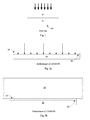
- FIG. 1 is a cross-sectional drawing of a prior art photovoltaic cell.
- FIGS. 2 a - 2 d are cross-sectional drawings of stages of fabrication of a photovoltaic cell formed according to an embodiment of U.S. patent application Ser. No. 12/026,530.
- FIGS. 3 a and 3 b are cross-sectional views illustrating inadvertent fabrication of a pinhole in a lamina and a corresponding column asperity in a donor wafer.
- FIGS. 4 a and 4 b are cross-sectional views illustrating inadvertent fabrication of an edge asperity during cleaving of a lamina from a donor wafer.
- FIGS. 5 a through 5 e are cross-sectional views illustrating preparation of a surface of a donor body for reuse following cleaving, according to an embodiment of the present invention.
- FIGS. 5 f and 5 g are cross-sectional views illustrating changes in the surface following growth and removal of oxide.
- FIGS. 6 a through 6 c are cross-sectional views showing stages in fabrication of a photovoltaic cell formed from a lamina cleaved from a silicon donor body.
- the donor body may be prepared for reuse before and after cleaving of the lamina according to embodiments of the present invention.
- FIG. 7 is a flowchart illustrating an embodiment of the present invention.
- a conventional prior art photovoltaic cell includes a p-n diode; an example is shown in FIG. 1 .
- a depletion zone forms at the p-n junction, creating an electric field.
- Incident photons incident light is indicated by arrows
- electrons tend to migrate toward the n region of the diode, while holes migrate toward the p region, resulting in current, called photocurrent.
- the dopant concentration of one region will be higher than that of the other, so the junction is either a n ⁇ /p+ junction (as shown in FIG. 1 ) or a p ⁇ /n+ junction.
- the more lightly doped region is known as the base of the photovoltaic cell, while the more heavily doped region is known as the emitter. Most carriers are generated within the base, and it is typically the thickest portion of the cell. The base and emitter together form the active region of the cell.
- the cell also frequently includes a heavily doped contact region in electrical contact with the base, and of the same conductivity type, to improve current flow. In the example shown in FIG. 1 , the heavily doped contact region is n-type.
- Sivaram et al. U.S. patent application Ser. No. 12/026,530, “Method to Form a Photovoltaic Cell Comprising a Thin Lamina,” filed Feb. 5, 2008, owned by the assignee of the present invention and hereby incorporated by reference, describes fabrication of a photovoltaic cell comprising a thin semiconductor lamina formed of non-deposited semiconductor material.
- a semiconductor donor wafer 20 is implanted through first surface 10 with one or more species of gas ions, for example hydrogen and/or helium ions.
- the implanted ions define a cleave plane 30 within the semiconductor donor wafer.
- gas ions for example hydrogen and/or helium ions
- donor wafer 20 is affixed at first surface 10 to receiver 60 .
- an anneal causes lamina 40 to cleave from donor wafer 20 at cleave plane 30 , creating second surface 62 .
- additional processing before and after the cleaving step forms a photovoltaic cell comprising semiconductor lamina 40 , which is between about 0.2 and about 100 microns thick, for example between about 0.2 and about 50 microns, for example between about 1 and about 20 microns thick, in some embodiments between about 1 and about 10 microns thick, though any thickness within the named range is possible.
- Receiver 60 may be a discrete receiver element having a maximum width no more than 50 percent greater than that of donor wafer 10 , and preferably about the same width, as described in Herner, U.S. patent application Ser. No. 12/057,265, “Method to Form a Photovoltaic Cell Comprising a Thin Lamina Bonded to a Discrete Receiver Element,” filed on Mar. 27, 2008, owned by the assignee of the present application and hereby incorporated by reference.
- a plurality of donor wafers may be affixed to a single, larger receiver, and a lamina cleaved from each donor wafer.
- the original donor wafer may be 200, 300, or more microns thick, and thus multiple laminae may be cleaved from it. Following exfoliation, however, the new surface of the donor wafer 20 typically is not sufficiently planar for immediate reuse. There are several causes for such nonplanarity. Referring to FIGS. 3 a and 3 b , if bonding is imperfect in any location, for example if a particle 102 was present between the bonding surfaces of donor wafer 20 and receiver element 60 , a pinhole 104 may form in lamina 40 during exfoliation at cleave plane 30 . The material left behind remains on the donor wafer as a column asperity 106 .
- the column asperity 106 in the shape of a pillar, usually has a height equal to the thickness of lamina 40 , and also typically includes any layers formed on first surface 10 before bonding. For example, the layers of stack 112 will remain at the top of column asperity 106 .
- FIG. 4 a shows the edge of donor wafer 20 and receiver element 60 when they are bonded, before cleaving.
- the edges of donor wafer 20 are typically beveled.
- the bevel distributes stress during routine handling and helps prevent breakage.
- exfoliation may occur successfully along cleave plane 30 only where the surfaces of donor wafer 20 (including any deposited layers on this surface, not shown) and receiver element 60 are bonded.
- An edge asperity 108 of material that failed to cleave at cleave plane 30 may remain where the beveled edge of donor wafer 20 did not meet the surface of receiver element 60 .
- FIG. 5 a shows a donor wafer 20 from which a lamina has been cleaved, leaving behind a column asperity 106 and an edge asperity 108 at new surface 45 .
- a stack 112 remains at the top of column asperity 106 and on edge asperity 108 .
- the stack 112 shown in FIG. 5 a is removed by etching.
- This stack typically includes conductive layers, and may also include one or more dielectric layers.
- the column and edge asperities are removed by mechanical grinding.
- FIG. 5 c shows this irregularity greatly exaggerated for visibility.
- an oxide 47 is grown on surface 45 , as shown in FIG. 5 d , then the oxide is chemically stripped, as in FIG. 5 e .
- the process of growing and removing oxide consumes silicon, removing grinding damage and any remaining exfoliation damage.
- the oxide growth and removal also tends to round the sharp points at surface 45 ; FIGS.
- 5 f and 5 g illustrate this effect, showing enlarged segments of surface 45 before and after oxide growth and removal, respectively.
- Rounding points creates very little difference in the actual peak-to-valley height of surface irregularity, but it has been found to provide unexpected improvement in bonding and exfoliation.
- Surface grinding, and growth and removal of oxide, are both relatively inexpensive processes.
- the surface of the donor body includes silicon asperities having relief of at least two microns, sometimes four, five or more microns.
- the surface is subjected to mechanical grinding to remove or reduce the asperities, then an oxide is grown and removed at the surface.
- ions are implanted through the surface to define a cleave plane within the donor body.
- no more than about ten microns of thickness of silicon is removed from the donor body, including the relief of the asperities.
- no more than about eight microns of thickness of silicon is removed from the donor body, including the relief of the asperities.
- No chemical-mechanical polishing is performed at the surface, and the grinding step does not include the use of a chemical etchant.
- An appropriate donor body may be a monocrystalline silicon wafer of any practical thickness, for example from about 200 to about 1000 microns thick. In alternative embodiments, the donor wafer may be thicker; maximum thickness is limited only by practicalities of wafer handling. Alternatively, polycrystalline or multicrystalline silicon may be used, as may microcrystalline silicon, or wafers or ingots of other semiconductor materials. It will be appreciated by those skilled in the art that the term “monocrystalline silicon” as it is customarily used will not exclude silicon with occasional flaws or impurities such as conductivity-enhancing dopants.
- the process of forming monocrystalline silicon generally results in circular wafers, but the donor body can have other shapes as well.
- cylindrical monocrystalline ingots are often machined to an octagonal cross section prior to cutting wafers.
- Wafers may also be other shapes, such as square.
- Square wafers have the advantage that, unlike circular or hexagonal wafers, they can be aligned edge-to-edge on a photovoltaic module with minimal unused gaps between them.
- the diameter or width of the wafer may be any standard or custom size. For simplicity this discussion will describe the use of a monocrystalline silicon wafer as the semiconductor donor body, but it will be understood that donor bodies of other types and materials can be used.
- donor wafer 20 is a monocrystalline silicon wafer which is lightly to moderately doped to a first conductivity type, for example an n-type wafer.
- Donor wafer 20 may be, for example, solar- or semiconductor-grade silicon.
- First surface 10 of donor wafer 20 may be substantially planar, or may have some preexisting texture. If desired, some texturing or roughening of first surface 10 may be performed, for example by wet etch or plasma treatment. Methods to create surface roughness are described in further detail in Petti, U.S. patent application Ser. No. 12/130,241, “Asymmetric Surface Texturing For Use in a Photovoltaic Cell and Method of Making,” filed May 30, 2008; and in Herner, U.S. patent application Ser. No. 12/343,420, “Method to Texture a Lamina Surface Within a Photovoltaic Cell,” filed Dec. 23, 2008, both owned by the assignee of the present application and both hereby incorporated by reference.
- First surface 10 may be heavily doped to the same conductivity type as wafer 20 , forming heavily doped region 14 ; in this example, heavily doped region 14 is n-type.
- This doping step can be performed by any conventional method, including diffusion doping. Doping and texturing can be performed in any order, but since most texturing methods remove some thickness of silicon, it may be preferred to form heavily doped n-type region 14 following texturing.
- dielectric layer 28 is formed on first surface 10 .
- dielectric layer 28 is silicon dioxide, for example, it may be between about 1000 and about 1500 angstroms thick. This layer may be grown or deposited by any suitable method.
- ions preferably hydrogen or a combination of hydrogen and helium
- dielectric layer 28 is implanted through dielectric layer 28 into wafer 20 to define cleave plane 30 , as described earlier.
- the cost of this hydrogen or helium implant may reduced by methods described in Parrill et al., U.S. patent application Ser. No. 12/122,108, “Ion Implanter for Photovoltaic Cell Fabrication,” filed May 16, 2008; or those of Ryding et al., U.S. patent application Ser. No. 12/494,268, “Ion Implantation Apparatus and a Method for Fluid Cooling,” filed Jun. 30, 2009, both owned by the assignee of the present invention and hereby incorporated by reference.
- the overall depth of cleave plane 30 is determined by several factors, including implant energy.
- the depth of cleave plane 30 can be between about 0.2 and about 100 microns from first surface 10 , for example between about 0.5 and about 20 or about 50 microns, for example between about 1 and about 10 microns or between about 1 or 2 microns and about 5 or 6 microns.
- openings 33 are formed in dielectric layer 28 by any appropriate method, for example by laser scribing or screen printing.
- a titanium layer 24 is formed on dielectric layer 28 by any suitable method, for example by sputtering or thermal evaporation. This layer may have any desired thickness, for example about 100 angstroms.
- Non-reactive barrier layer 26 is formed on and in immediate contact with titanium layer 24 .
- Suitable materials for non-reactive barrier layer include TiW, TiN, W, Ta, TaN, TaSiN, or alloys thereof.
- the thickness of non-reactive barrier layer 26 may be about 1000 angstroms thick.
- Low-resistance layer 22 is formed on non-reactive barrier layer 26 . This layer may be, for example, silver, cobalt, or tungsten or alloys thereof. In this example low-resistance layer 22 is silver. Silver layer 22 may be about 20,000 angstroms (2 microns) thick.
- an adhesion layer 32 is formed on low-resistance layer 22 .
- Adhesion layer 32 is a material that will adhere to receiver element 60 , for example titanium. In some embodiments, adhesion layer 32 is about 400 angstroms.
- receiver element 60 may be any suitable material, including glass, such as soda-lime glass or borosilicate glass; a metal or metal alloy such as stainless steel or aluminum; a polymer; or a semiconductor, such as metallurgical grade silicon.
- glass such as soda-lime glass or borosilicate glass
- metal or metal alloy such as stainless steel or aluminum
- polymer such as polyethylene
- semiconductor such as metallurgical grade silicon.
- a thermal step causes lamina 40 to cleave from donor wafer 20 at the cleave plane.
- this cleaving step may be combined with a bonding step.
- Cleaving is achieved in this example by exfoliation, which may be achieved at temperatures between, for example, about 350 and about 650 degrees C.
- the thickness of lamina 40 is determined by the depth of cleave plane 30 . In many embodiments, the thickness of lamina 40 is between about 1 and about 10 microns, for example between about 2 and about 5 microns, for example at least three microns. Following exfoliation, processing continues to fabricate a photovoltaic cell including lamina 40 , as will be described.
- FIG. 5 a shows new surface 45 of donor wafer 20 , which was created by exfoliation. Note this surface cannot practically be drawn to scale.
- Surface 45 includes column asperities 106 and edge asperity 108 .
- the relief of column asperities 106 and edge asperity 108 will typically be the thickness of the exfoliated lamina and the thickness of the grown and deposited stack 112 formed on the original surface of donor wafer 20 before bonding.
- deposited stack 112 includes (referring to FIG. 6 b ) dielectric layer 28 , titanium layer 24 , non-reactive barrier layer 26 , silver layer 22 , and adhesion layer 32 .
- the layers disposed between the lamina and the receiver element will vary, and thus the materials in deposited layers 112 at the top of column asperities 106 and edge asperity 108 immediately following exfoliation will vary as well.
- deposited layers 112 are removed, for example, by a simple wet etch. Etching may be performed with hydrofluoric acid, or a compound including hydrofluoric acid, until only silicon remains. Depending on the materials used for deposited layers 112 , other etchants, or combination of etchants, may be used. Aqua regia or an electro-chemical etch may be employed. Little or no silicon is removed by this etching process.
- column asperities 106 and edge asperity 108 are removed by mechanical grinding. Grinding is done by any appropriate method. In one example, grinding may be done using an abrasive wheel with between 4000 and 6000 grit. The grinding process may be rotational, through-feed, or a combined process. For rotational grinding, typical grinding wheel speeds are between 1000 and 6500 rpm, while wafer rotational speeds range between 40 and 600 rpm. Either the grinding wheel, the wafer, or both may rotate. For through-feed grinding, the rotational speeds of the grinding wheel are similar to those used in rotational grinding. The linear travel speed of the grinding wheel and/or the wafer may be, for example, between 50 and 2000 mm/min. These different approaches achieve different surface finish. Diamond, silicon carbide, or any other suitable abrasive may be used.
- the grinding step may itself leave contaminants at surface 45 .
- a cleaning step is performed at surface 45 to remove these contaminants.
- This cleaning step may include an etch step. This cleaning etch removes minimal thickness, for example no more than 1000 angstroms, and generally far less.
- silicon dioxide layer 47 is grown at surface 45 . Any suitable oxidation method may be used. In some embodiments, a wet oxide is performed at between 1000 and 1100 degrees C. Between about 0.5 and about 2 microns of silicon dioxide is grown, for example about 1 micron. Growing one micron of silicon dioxide consumes about 4000 angstroms of silicon. In alternative embodiments, silicon dioxide layer 47 could be replaced with a grown layer of some other suitable material, for example silicon oxynitride.
- oxide layer 47 is then removed, for example by a hydrofluoric acid dip.
- FIG. 5 f shows surface 45 immediately after grinding
- FIG. 5 g shows the surface following oxide removal.
- the process of growing and removing oxide layer 47 at surface 45 has very little effect on the peak-to-valley relief of surface 45 , but tends to round the sharp peaks.
- the peak-to-valley relief of surface 45 will typically be about 250 angstroms or less, for example between about 50 and about 250 angstroms.
- the donor wafer can be reused to form an additional lamina, for example in the fabrication steps described earlier and illustrated in FIGS. 6 a through 6 c .
- FIG. 6 c recall that dielectric layer 28 , titanium layer 24 , non-reactive barrier layer 26 , silver layer 22 , and adhesion layer 32 were formed on treated surface 45 , and, following bonding to receiver element 60 , lamina 40 was cleaved from the donor wafer.
- additional processing completes a photovoltaic cell comprising lamina 40 .
- intrinsic amorphous silicon layer 72 may be deposited on second surface 62 , which was created by exfoliation, and heavily doped amorphous silicon layer 74 follows, serving as the emitter of the cell.
- a transparent conductive oxide layer 110 is formed next, and electrical contacts 57 complete the cell. Fabrication of this cell is described in detail in Herner, U.S. patent application Ser. No. 12/540,463, “Intermetal Stack For Use in a Photovoltaic Device,” filed Aug. 13, 2009, owned by the assignee of the present application, and hereby incorporated by reference. It has been found that rounding the peaks of topography at the treated surface aids in bonding of the donor wafer to the receiver element and cleaving of the lamina from the donor wafer.
- the methods of the present invention can be used to treat the surface of a donor wafer both after cleaving of a first lamina and before cleaving of a second lamina.
- thermally cleaving a first lamina from the donor wafer creating an exfoliated surface of the donor wafer; mechanically grinding the exfoliated surface to remove or reduce asperities; growing oxide on the exfoliated surface; etching to remove the oxide; implanting ions through the exfoliated surface to define a cleave plane within the donor wafer; thermally cleaving a second lamina from the donor wafer at the cleave plane, wherein the second lamina is suitable for use in a photovoltaic cell.
- a photovoltaic cell may be fabricated, for example using the methods of Sivaram et al., wherein the photovoltaic cell comprises the second lamina.
- FIG. 7 summarizes these process steps.
Abstract
Description
Claims (14)
Priority Applications (1)
| Application Number | Priority Date | Filing Date | Title |
|---|---|---|---|
| US12/557,379 US8871109B2 (en) | 2009-04-28 | 2009-09-10 | Method for preparing a donor surface for reuse |
Applications Claiming Priority (2)
| Application Number | Priority Date | Filing Date | Title |
|---|---|---|---|
| US17358409P | 2009-04-28 | 2009-04-28 | |
| US12/557,379 US8871109B2 (en) | 2009-04-28 | 2009-09-10 | Method for preparing a donor surface for reuse |
Publications (2)
| Publication Number | Publication Date |
|---|---|
| US20100273329A1 US20100273329A1 (en) | 2010-10-28 |
| US8871109B2 true US8871109B2 (en) | 2014-10-28 |
Family
ID=42992522
Family Applications (1)
| Application Number | Title | Priority Date | Filing Date |
|---|---|---|---|
| US12/557,379 Expired - Fee Related US8871109B2 (en) | 2009-04-28 | 2009-09-10 | Method for preparing a donor surface for reuse |
Country Status (1)
| Country | Link |
|---|---|
| US (1) | US8871109B2 (en) |
Cited By (3)
| Publication number | Priority date | Publication date | Assignee | Title |
|---|---|---|---|---|
| US11235389B2 (en) | 2018-09-19 | 2022-02-01 | Molyworks Materials Corp. | Deployable manufacturing center (DMC) system and process for manufacturing metal parts |
| US11590574B2 (en) | 2018-12-18 | 2023-02-28 | Molyworks Materials Corp. | Method for manufacturing metal components using recycled feedstock and additive manufacturing |
| US11623278B2 (en) | 2019-07-10 | 2023-04-11 | MolyWorks Materials Corporation | Expeditionary additive manufacturing (ExAM) system and method |
Families Citing this family (10)
| Publication number | Priority date | Publication date | Assignee | Title |
|---|---|---|---|---|
| US8178419B2 (en) | 2008-02-05 | 2012-05-15 | Twin Creeks Technologies, Inc. | Method to texture a lamina surface within a photovoltaic cell |
| US8916954B2 (en) | 2012-02-05 | 2014-12-23 | Gtat Corporation | Multi-layer metal support |
| US8841161B2 (en) | 2012-02-05 | 2014-09-23 | GTAT.Corporation | Method for forming flexible solar cells |
| US20130330871A1 (en) * | 2012-06-12 | 2013-12-12 | Twin Creeks Technologies, Inc. | Methods for texturing a semiconductor material |
| US8785294B2 (en) | 2012-07-26 | 2014-07-22 | Gtat Corporation | Silicon carbide lamina |
| US11721547B2 (en) * | 2013-03-14 | 2023-08-08 | Infineon Technologies Ag | Method for manufacturing a silicon carbide substrate for an electrical silicon carbide device, a silicon carbide substrate and an electrical silicon carbide device |
| CN105518861B (en) | 2013-06-20 | 2018-10-02 | 斯坦舍有限公司 | Gate controlled charge modulation device for cmos sensor |
| KR20160094416A (en) * | 2013-12-02 | 2016-08-09 | 주식회사 스트라티오코리아 | Layer transfer technology for silicon carbide |
| US20180033609A1 (en) * | 2016-07-28 | 2018-02-01 | QMAT, Inc. | Removal of non-cleaved/non-transferred material from donor substrate |
| US20180019169A1 (en) * | 2016-07-12 | 2018-01-18 | QMAT, Inc. | Backing substrate stabilizing donor substrate for implant or reclamation |
Citations (11)
| Publication number | Priority date | Publication date | Assignee | Title |
|---|---|---|---|---|
| US6010579A (en) | 1997-05-12 | 2000-01-04 | Silicon Genesis Corporation | Reusable substrate for thin film separation |
| US6103599A (en) | 1997-07-25 | 2000-08-15 | Silicon Genesis Corporation | Planarizing technique for multilayered substrates |
| US6153014A (en) * | 1997-08-26 | 2000-11-28 | Samsung Electronics Co., Ltd. | Method of cleaning a silicon wafer using a standard cleaning solution |
| US20050164471A1 (en) * | 2003-08-12 | 2005-07-28 | Christophe Maleville | Method for producing thin layers of semiconductor material from a donor wafer |
| US20060115986A1 (en) * | 2004-11-26 | 2006-06-01 | Applied Materials, Inc. | Edge removal of silicon-on-insulator transfer wafer |
| US20060118935A1 (en) * | 2003-04-02 | 2006-06-08 | Eiji Kamiyama | Laminated semiconductor substrate process for producing the same |
| US20080124929A1 (en) * | 2005-11-28 | 2008-05-29 | Hidehiko Okuda | Process for Regenerating Layer Transferred Wafer and Layer Transferred Wafer Regenerated by the Process |
| WO2008107029A1 (en) * | 2007-02-16 | 2008-09-12 | S.O.I.Tec Silicon On Insulator Technologies | Method of bonding two substrates |
| EP2015354A1 (en) | 2007-07-11 | 2009-01-14 | S.O.I.Tec Silicon on Insulator Technologies | Method for recycling a substrate, laminated wafer fabricating method and suitable recycled donor substrate |
| US7531428B2 (en) | 2004-11-09 | 2009-05-12 | S.O.I.Tec Silicon On Insulator Technologies | Recycling the reconditioned substrates for fabricating compound material wafers |
| US20090194162A1 (en) | 2008-02-05 | 2009-08-06 | Twin Creeks Technologies, Inc. | Method to form a photovoltaic cell comprising a thin lamina |
-
2009
- 2009-09-10 US US12/557,379 patent/US8871109B2/en not_active Expired - Fee Related
Patent Citations (15)
| Publication number | Priority date | Publication date | Assignee | Title |
|---|---|---|---|---|
| US6146979A (en) * | 1997-05-12 | 2000-11-14 | Silicon Genesis Corporation | Pressurized microbubble thin film separation process using a reusable substrate |
| US6159825A (en) | 1997-05-12 | 2000-12-12 | Silicon Genesis Corporation | Controlled cleavage thin film separation process using a reusable substrate |
| US6335264B1 (en) | 1997-05-12 | 2002-01-01 | Silicon Genesis Corporation | Controlled cleavage thin film separation process using a reusable substrate |
| US6010579A (en) | 1997-05-12 | 2000-01-04 | Silicon Genesis Corporation | Reusable substrate for thin film separation |
| US6103599A (en) | 1997-07-25 | 2000-08-15 | Silicon Genesis Corporation | Planarizing technique for multilayered substrates |
| US6153014A (en) * | 1997-08-26 | 2000-11-28 | Samsung Electronics Co., Ltd. | Method of cleaning a silicon wafer using a standard cleaning solution |
| US20060118935A1 (en) * | 2003-04-02 | 2006-06-08 | Eiji Kamiyama | Laminated semiconductor substrate process for producing the same |
| US20050164471A1 (en) * | 2003-08-12 | 2005-07-28 | Christophe Maleville | Method for producing thin layers of semiconductor material from a donor wafer |
| US7531428B2 (en) | 2004-11-09 | 2009-05-12 | S.O.I.Tec Silicon On Insulator Technologies | Recycling the reconditioned substrates for fabricating compound material wafers |
| US20060115986A1 (en) * | 2004-11-26 | 2006-06-01 | Applied Materials, Inc. | Edge removal of silicon-on-insulator transfer wafer |
| US20080124929A1 (en) * | 2005-11-28 | 2008-05-29 | Hidehiko Okuda | Process for Regenerating Layer Transferred Wafer and Layer Transferred Wafer Regenerated by the Process |
| WO2008107029A1 (en) * | 2007-02-16 | 2008-09-12 | S.O.I.Tec Silicon On Insulator Technologies | Method of bonding two substrates |
| US20100093152A1 (en) * | 2007-02-16 | 2010-04-15 | Kerdiles Sebastien | Method of bonding two substrates |
| EP2015354A1 (en) | 2007-07-11 | 2009-01-14 | S.O.I.Tec Silicon on Insulator Technologies | Method for recycling a substrate, laminated wafer fabricating method and suitable recycled donor substrate |
| US20090194162A1 (en) | 2008-02-05 | 2009-08-06 | Twin Creeks Technologies, Inc. | Method to form a photovoltaic cell comprising a thin lamina |
Non-Patent Citations (9)
| Title |
|---|
| Chao, Choung-Li et al., "A Study on the Surface Integrity of Single Crystal Silicon Ground by CIFB-Diamond Wheels (ELID) and Resin-Bonded Diamond Wheels", Proceedings of Tamkang University, Tamsui, Taipei, Taiwan, 2005 International Nano and MEMS Workshop, Nov. 23-24, 2005, pp. 75-78. |
| Chao, Choung-Li et al., "A Study on the Surface Integrity of Single Crystal Silicon Ground by CIFB—Diamond Wheels (ELID) and Resin-Bonded Diamond Wheels", Proceedings of Tamkang University, Tamsui, Taipei, Taiwan, 2005 International Nano and MEMS Workshop, Nov. 23-24, 2005, pp. 75-78. |
| Chidambaram, Somasundaram et al., "A Study of Grinding Marks in Semiconductor Wafer Grinding," American Society for Precision Engineering, Proceedings ASPE 2001 Annual Meeting. |
| GSI Westwind, Wafer Grinding, Air Bearings, tool specification. |
| Haapalinna, Atte et al., "Rotational grinding of silicon wafers-sub-surface damage inspection," Materials Science and Engineering B107 (2004), pp. 321-331. |
| Haapalinna, Atte et al., "Rotational grinding of silicon wafers—sub-surface damage inspection," Materials Science and Engineering B107 (2004), pp. 321-331. |
| Sun, Wangping, Grinding of Silicon Wafers: Wafer Shape Model and Its Applications, PhD Dissertation, Department of Industrial and Manufacturing Systems Engineering, College of Engineering, Kansas State University, 2005. |
| Yang, Yu et al., "Process induced sub-surface damage in mechanically ground silicon wafers," Semicond. Sci. Technolo. 23 (2008), 075038, pp. 1-10. |
| Young, H-T et al., "Precision wafer thinning and its surface conditioning technique," Int. J. Materials and Product Technology, vol. 31, No. 1, 2008, pp. 36-45. |
Cited By (5)
| Publication number | Priority date | Publication date | Assignee | Title |
|---|---|---|---|---|
| US11235389B2 (en) | 2018-09-19 | 2022-02-01 | Molyworks Materials Corp. | Deployable manufacturing center (DMC) system and process for manufacturing metal parts |
| US11679438B2 (en) | 2018-09-19 | 2023-06-20 | MolyWorks Materials Corporation | Process for manufacturing metal parts using deployable manufacturing center (DMC) system |
| US11590574B2 (en) | 2018-12-18 | 2023-02-28 | Molyworks Materials Corp. | Method for manufacturing metal components using recycled feedstock and additive manufacturing |
| US11623278B2 (en) | 2019-07-10 | 2023-04-11 | MolyWorks Materials Corporation | Expeditionary additive manufacturing (ExAM) system and method |
| US11872634B2 (en) | 2019-07-10 | 2024-01-16 | MolyWorks Material Corporation | Expeditionary additive manufacturing (ExAM) method |
Also Published As
| Publication number | Publication date |
|---|---|
| US20100273329A1 (en) | 2010-10-28 |
Similar Documents
| Publication | Publication Date | Title |
|---|---|---|
| US8871109B2 (en) | Method for preparing a donor surface for reuse | |
| US20110073175A1 (en) | Photovoltaic cell comprising a thin lamina having emitter formed at light-facing and back surfaces | |
| TWI440201B (en) | Method to form a photovoltaic cell comprising a thin lamina | |
| WO2002061851A1 (en) | Solar cell and method for producing the same | |
| EP1059663A2 (en) | Process for producing a semiconductor thin film with a bonding and separating steps, solar cell fabrication and anodizing apparatus | |
| US20100229928A1 (en) | Back-contact photovoltaic cell comprising a thin lamina having a superstrate receiver element | |
| US7858430B2 (en) | Method for making a photovoltaic cell comprising contact regions doped through a lamina | |
| TWI474489B (en) | Photovoltaic cell comprising a thin lamina having a rear junction and method of making | |
| EP4128329B1 (en) | Method for manufacturing a composite structure comprising a thin layer made of monocrystalline sic on a carrier substrate made of sic | |
| TW202141582A (en) | PROCESS FOR MANUFACTURING A COMPOSITE STRUCTURE COMPRISING A THIN LAYER MADE OF MONOCRYSTALLINESiC ON A CARRIER SUBSTRATE MADE OF SiC | |
| US10559471B2 (en) | Method of manufacturing bonded wafer | |
| US20100224238A1 (en) | Photovoltaic cell comprising an mis-type tunnel diode | |
| US20130330871A1 (en) | Methods for texturing a semiconductor material | |
| US8501522B2 (en) | Intermetal stack for use in a photovoltaic cell | |
| JP3602323B2 (en) | Solar cell manufacturing method | |
| KR20110059366A (en) | Single crystalline semiconductor substrate having isolation region, solar cell using the same and manufacturing method thereof | |
| US8049104B2 (en) | Intermetal stack for use in a photovoltaic cell | |
| US7994064B2 (en) | Selective etch for damage at exfoliated surface | |
| US8633374B2 (en) | Photovoltaic cell comprising contact regions doped through a lamina | |
| US8349626B2 (en) | Creation of low-relief texture for a photovoltaic cell | |
| JP2011066213A (en) | Photoelectric converter and method of manufacturing the same | |
| EP2088633A2 (en) | Method to form a photovoltaic cell comprising a thin lamina | |
| JP5434806B2 (en) | Manufacturing method of semiconductor device | |
| JP2002305313A (en) | Solar battery |
Legal Events
| Date | Code | Title | Description |
|---|---|---|---|
| AS | Assignment |
Owner name: TWIN CREEKS TECHNOLOGIES, INC., CALIFORNIA Free format text: ASSIGNMENT OF ASSIGNORS INTEREST;ASSIGNORS:PRABHU, GOPAL;JACKSON, KATHY J.;LELAND, ORION;AND OTHERS;REEL/FRAME:023256/0259 Effective date: 20090909 |
|
| AS | Assignment |
Owner name: SILICON VALLEY BANK, CALIFORNIA Free format text: SECURITY INTEREST;ASSIGNOR:TWIN CREEKS TECHNOLOGIES, INC.;REEL/FRAME:029124/0057 Effective date: 20120914 |
|
| AS | Assignment |
Owner name: GTAT CORPORATION, NEW HAMPSHIRE Free format text: ASSIGNMENT OF ASSIGNORS INTEREST;ASSIGNORS:SILICON VALLEY BANK;TWIN CREEKS TECHNOLOGIES, INC.;REEL/FRAME:029275/0076 Effective date: 20121108 |
|
| AS | Assignment |
Owner name: NEUTRON THERAPEUTICS INC., MASSACHUSETTS Free format text: ASSIGNMENT OF ASSIGNORS INTEREST;ASSIGNOR:GTAT CORPORATION D/B/A GT ADVANCED TECHNOLOGIES;REEL/FRAME:037047/0004 Effective date: 20151103 |
|
| FEPP | Fee payment procedure |
Free format text: MAINTENANCE FEE REMINDER MAILED (ORIGINAL EVENT CODE: REM.) |
|
| LAPS | Lapse for failure to pay maintenance fees |
Free format text: PATENT EXPIRED FOR FAILURE TO PAY MAINTENANCE FEES (ORIGINAL EVENT CODE: EXP.); ENTITY STATUS OF PATENT OWNER: LARGE ENTITY |
|
| STCH | Information on status: patent discontinuation |
Free format text: PATENT EXPIRED DUE TO NONPAYMENT OF MAINTENANCE FEES UNDER 37 CFR 1.362 |
|
| FP | Lapsed due to failure to pay maintenance fee |
Effective date: 20181028 |
|
| AS | Assignment |
Owner name: NEUTRON THERAPEUTICS LLC, MASSACHUSETTS Free format text: CHANGE OF NAME;ASSIGNOR:NEUTRON THERAPEUTICS, INC.;REEL/FRAME:063662/0362 Effective date: 20230227 |