US8874050B1 - Saturation correction without using saturation detection and saturation prevention for a power amplifier - Google Patents
Saturation correction without using saturation detection and saturation prevention for a power amplifier Download PDFInfo
- Publication number
- US8874050B1 US8874050B1 US12/774,155 US77415510A US8874050B1 US 8874050 B1 US8874050 B1 US 8874050B1 US 77415510 A US77415510 A US 77415510A US 8874050 B1 US8874050 B1 US 8874050B1
- Authority
- US
- United States
- Prior art keywords
- signal
- power
- voltage
- amplifier circuitry
- output
- Prior art date
- Legal status (The legal status is an assumption and is not a legal conclusion. Google has not performed a legal analysis and makes no representation as to the accuracy of the status listed.)
- Active, expires
Links
Images


Classifications
-
- H—ELECTRICITY
- H01—ELECTRIC ELEMENTS
- H01P—WAVEGUIDES; RESONATORS, LINES, OR OTHER DEVICES OF THE WAVEGUIDE TYPE
- H01P5/00—Coupling devices of the waveguide type
- H01P5/12—Coupling devices having more than two ports
- H01P5/16—Conjugate devices, i.e. devices having at least one port decoupled from one other port
- H01P5/18—Conjugate devices, i.e. devices having at least one port decoupled from one other port consisting of two coupled guides, e.g. directional couplers
- H01P5/184—Conjugate devices, i.e. devices having at least one port decoupled from one other port consisting of two coupled guides, e.g. directional couplers the guides being strip lines or microstrips
-
- H—ELECTRICITY
- H03—ELECTRONIC CIRCUITRY
- H03F—AMPLIFIERS
- H03F1/00—Details of amplifiers with only discharge tubes, only semiconductor devices or only unspecified devices as amplifying elements
- H03F1/02—Modifications of amplifiers to raise the efficiency, e.g. gliding Class A stages, use of an auxiliary oscillation
- H03F1/0205—Modifications of amplifiers to raise the efficiency, e.g. gliding Class A stages, use of an auxiliary oscillation in transistor amplifiers
- H03F1/0211—Modifications of amplifiers to raise the efficiency, e.g. gliding Class A stages, use of an auxiliary oscillation in transistor amplifiers with control of the supply voltage or current
-
- H—ELECTRICITY
- H03—ELECTRONIC CIRCUITRY
- H03F—AMPLIFIERS
- H03F3/00—Amplifiers with only discharge tubes or only semiconductor devices as amplifying elements
- H03F3/189—High frequency amplifiers, e.g. radio frequency amplifiers
- H03F3/19—High frequency amplifiers, e.g. radio frequency amplifiers with semiconductor devices only
- H03F3/195—High frequency amplifiers, e.g. radio frequency amplifiers with semiconductor devices only in integrated circuits
-
- H—ELECTRICITY
- H03—ELECTRONIC CIRCUITRY
- H03F—AMPLIFIERS
- H03F3/00—Amplifiers with only discharge tubes or only semiconductor devices as amplifying elements
- H03F3/20—Power amplifiers, e.g. Class B amplifiers, Class C amplifiers
- H03F3/24—Power amplifiers, e.g. Class B amplifiers, Class C amplifiers of transmitter output stages
-
- H—ELECTRICITY
- H03—ELECTRONIC CIRCUITRY
- H03F—AMPLIFIERS
- H03F3/00—Amplifiers with only discharge tubes or only semiconductor devices as amplifying elements
- H03F3/68—Combinations of amplifiers, e.g. multi-channel amplifiers for stereophonics
-
- H—ELECTRICITY
- H03—ELECTRONIC CIRCUITRY
- H03H—IMPEDANCE NETWORKS, e.g. RESONANT CIRCUITS; RESONATORS
- H03H7/00—Multiple-port networks comprising only passive electrical elements as network components
- H03H7/38—Impedance-matching networks
-
- H—ELECTRICITY
- H03—ELECTRONIC CIRCUITRY
- H03F—AMPLIFIERS
- H03F2200/00—Indexing scheme relating to amplifiers
- H03F2200/541—Transformer coupled at the output of an amplifier
Definitions
- the present disclosure relates to power amplifiers, and particularly to controlling the saturation levels of power amplifiers to maintain desirable switching spectrums for the power amplifiers' outputs.
- GSM Global System for Mobile Communications
- DCS Digital Cellular System
- PCS Personal Communications Services
- a key component common to all radiotelephones is a radio frequency (RF) power amplifier (PA).
- PAs receive as input a modulated RF carrier.
- the radio frequency carrier is what “carries” digital information such as digitized voice or data to a cellular base station.
- the RF carrier Before reaching the PA, the RF carrier is too weak to be received by a cellular base station. Therefore, it is the function of the PA to boost the power of the RF carrier to a level sufficient for reception by a cellular base station.
- the adjustable power control signal In GSM radiotelephones, the adjustable power control signal must comply with a specification known as a “burst mask.”
- the burst mask specifies the rise time, fall time, duration, and power levels associated with the adjustable power control signal.
- the GSM signal consists of eight equal time slots. Each time slot must conform to the burst mask specification.
- the output of an integrator circuit may be used to control the ramp-up time and ramp-down time of a PA control signal that is responsive to a dynamic baseband signal known as V RAMP .
- V RAMP dynamic baseband signal
- the amplitude of V RAMP dictates that the output power of the PA must conform to the shape of the burst mask.
- V RAMP When the burst is completed, V RAMP needs to ramp down. However, the integrator circuit output voltage will have to first fall from the maximum possible voltage level, as shown in FIG. 2 . During the time it takes for the integrator circuit output voltage to begin to fall, the PA output power will not immediately follow V RAMP down. However, once V RAMP decreases to a voltage level in which the PA is once again controllable, the integrator circuit output voltage must “catch up” with V RAMP . As a result, there will be a sharp drop in the PA's output power, as shown in FIG. 3 . As illustrated in FIG. 4 , this sharp drop in the PA's output power typically results in failure of the European Telecommunications Standards Institute (ETSI) switching spectrum specification. Notice that both the ⁇ 400 kHz signal and the +400 kHz signal exceed the ETSI limit as V RAMP descends.
- ETSI European Telecommunications Standards Institute
- the present disclosure provides for control of a power amplifier (PA).
- PA power amplifier
- the present disclosure provides a power control circuit and method that provide a saturation correction for a PA in order to maintain a desirable switching spectrum.
- the power control circuit includes a closed loop system that is responsive to a dynamic baseband signal known as V RAMP .
- V RAMP dynamic baseband signal
- the dynamic baseband signal (V RAMP ) has an amplitude that dictates the amount of output power delivered by the PA.
- the method samples a feedback signal from the PA in order to capture a sample value, such as a detector voltage, that represents the output of the PA when V RAMP is at or near a maximum level.
- a fixed dc signal has a magnitude that is derived from the sample value by subtracting a predetermined value from the sample value.
- the fixed dc signal is applied as a new PA control signal in place of the dynamic baseband signal (V RAMP ).
- the predetermined value is selected to decrease the output power of the PA by a fraction of a decibel (dB).
- an integrator circuit comprising the closed loop system will force the feedback signal from the PA to equal the fixed dc signal.
- the saturation of the PA will be compensated without using a circuit or method for detecting PA saturation.
- the amplitude of the dynamic baseband signal (V RAMP ) decreases, the dynamic baseband signal (V RAMP ) is reapplied as a dynamic PA control signal in place of the fixed dc signal. In this way, the PA will not experience an abrupt control input that would generate an undesirable switching spectrum.
- a saturation prevention method is disclosed that can cooperate with the above disclosed power control circuit and method in order to eliminate the possibility of undesirable power reductions for abnormal operating conditions, such as a low battery voltage supply to the PA being controlled.
- the power control circuit may be selectably enabled by a baseband control system to automatically reduce a fixed output power of the PA by a predetermined amount of offset power for power levels above a given power level during transmission of an RF signal.
- the fixed output power is maintained, not reduced, for power levels below the given power level.
- the power levels available to the PA that are above the given power level are calibrated to include the predetermined amount of offset power. In this way, PA output power at power levels above the given power level will be reduced to a desirable magnitude, whereas PA output power at levels below the given power level will be maintained at a desirable magnitude even in abnormal operating conditions such as a low battery voltage supply for the PA, etc.
- FIG. 1 depicts power amplifier (PA) control signal waveforms associated with the beginning of a GSM burst.
- PA power amplifier
- FIG. 2 depicts PA control signal waveforms associated with the end of a GSM burst.
- FIG. 3 depicts an undesirable effect of saturation on a PA output power at the end of the GSM burst as the voltage of the PA control signal drops steeply.
- FIG. 4 illustrates a severe degradation of the output switching spectrum due to a steep change in PA power output.
- FIG. 5 depicts a mobile terminal having PA control circuitry according to an embodiment of the present disclosure.
- FIG. 6 is a flowchart that illustrates a method according to the present disclosure for correcting a saturation of a PA.
- FIG. 7 depicts the response of the PA control signal waveforms to the method of FIG. 6 at the beginning of a GSM burst.
- FIG. 8 depicts the response of the PA control signal waveforms to the method of FIG. 6 at the end of a GSM burst.
- FIG. 9 illustrates the improved output switching spectrum resulting from the implementation of the method of FIG. 6 .
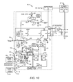
- FIG. 10 is a detailed schematic of the power control circuitry of FIG. 5 that is in accordance with the present disclosure.
- FIG. 11 is a graph of PA output power versus battery voltage illustrating the results of the saturation prevention method combined with the saturation correction method.
- FIG. 12 is a graph of PA output power versus battery voltage illustrating the results of the saturation correction method without the saturation prevention method.
- FIG. 13 is a graph of +/ ⁇ 400 kHz switching spectrum versus battery voltage.
- an embodiment of the present disclosure is preferably incorporated in a mobile terminal 20 , such as a mobile telephone, personal digital assistant (PDA), or the like.
- the basic architecture of the mobile terminal 20 may include a receiver front end 22 , a radio frequency (RF) transmitter section 24 , an antenna 26 , a duplexer or switch 28 , a baseband processor 30 , a control system 32 , a frequency synthesizer 34 , and an interface 36 .
- the receiver front end 22 receives information bearing RF signals from one or more remote transmitters provided by a base station.
- a low noise amplifier (LNA) 37 amplifies the signal.
- LNA low noise amplifier
- a filter circuit 38 minimizes broadband interference in the received signal, while a downconverter 40 downconverts the filtered received signal to an intermediate or baseband frequency signal, which is then digitized into one or more digital streams.
- the receiver front end 22 typically uses one or more mixing frequencies generated by the frequency synthesizer 34 .
- the baseband processor 30 processes the digitized received signal to extract the information or data bits conveyed in the received signal. This processing typically comprises demodulation, decoding, and error correction operations. As such, the baseband processor 30 is generally implemented in one or more digital signal processors (DSPs).
- DSPs digital signal processors
- the baseband processor 30 receives digitized data from the control system 32 , which it encodes for transmission.
- the encoded data is output to the RF transmitter section 24 , where it is used by a modulator 42 to modulate a carrier signal that is at a desired transmit frequency.
- Power amplifier circuitry 44 amplifies the modulated carrier signal to a level appropriate for transmission from the antenna 26 .
- the power amplifier circuitry 44 provides gain for the signal to be transmitted under control of power control circuitry 46 , which is preferably controlled by the control system 32 using the V RAMP signal.
- a detector circuit 47 provides a feedback signal (V DET ) from the output of the power amplifier circuitry 44 to the power control circuitry 46 .
- V DET feedback signal
- the bias for the power amplifier circuitry 44 is relatively stable regardless of power, and varying the voltage supplied to the power amplifier circuitry 44 controls actual power levels.
- the control system 32 may also provide a transmit enable (TX ENABLE) signal to effectively turn the power amplifier circuitry 44 and power control circuitry 46 on during periods of transmission.
- the control system 32 may also include a general purpose input/output (GPIO) signal line for sending commands and data to the power control circuitry 44 .
- GPIO general purpose input/output
- a user may interact with the mobile terminal 20 via the interface 36 , which may include interface circuitry 48 associated with a microphone 50 , a speaker 52 , a keypad 54 , and a display 56 .
- the interface circuitry 48 typically includes analog-to-digital converters, digital-to-analog converters, amplifiers, and the like. Additionally, it may include a voice encoder/decoder, in which case it may communicate directly with the baseband processor 30 .
- the microphone 50 will typically convert audio input, such as the user's voice, into an electrical signal, which is then digitized and passed directly or indirectly to the baseband processor 30 . Audio information encoded in the received signal is recovered by the baseband processor 30 , and is converted into an analog signal suitable for driving speaker 52 by the input/output and interface circuitry 48 .
- the keypad 54 and display 56 enable the user to interact with the mobile terminal 20 by inputting numbers to be dialed, address book information, or the like, and monitoring call progress information.
- the disclosed saturation correction method begins with a dynamic baseband signal (V RAMP ) that linearly increases from an initial voltage such as a pedestal of a few tenths of a volt (step 120 ).
- V RAMP dynamic baseband signal
- the control system 32 FIG. 5
- the power control circuitry 46 receives the V RAMP signal as input, and in turn integrates the V RAMP signal with the feedback signal (V DET ) to produce an output to the power amplifier circuitry 44 (step 122 ).
- the detector circuit 47 ( FIG. 5 ) provides the feedback signal V DET , which in this case is not used to detect PA saturation.
- An inherent delay is maintained until the V RAMP signal increases to a voltage level that is above a predetermined voltage level (step 124 ).
- the predetermined voltage level corresponds to a PA output power that is slightly greater than 20 dBm.
- a predetermined delay is initiated (step 126 ).
- the predetermined delay is preferably around 120 microseconds ( ⁇ S). Other values of delay can be used depending on a user's particular baseband application.
- a sample voltage of the feedback signal V DET is captured once the predetermined delay has expired (step 128 ).
- the control of the output from the power amplifier circuitry 44 via the dynamic V RAMP signal is removed while a constant voltage equal to the V RAMP sample voltage is maintained as output to the power amplifier circuitry 44 (step 130 ).
- a value of voltage equal to the V DET sample voltage minus a predetermined offset voltage is applied to the power amplifier circuitry 44 (step 132 ).
- the predetermined offset voltage is selected such that the PA of the power amplifier circuitry 44 is slightly below the saturated power level at the time the dynamic V RAMP signal is removed from controlling the output of the power control circuitry 46 .
- a preferred offset voltage value is selectable to decrease the amount output power delivered by the power amplifier circuitry 44 during saturation by a fraction of a dBm.
- the V RAMP signal reaches a maximum voltage level and begins a voltage decrease.
- An output voltage of the power control circuitry 46 is maintained with the level of the V DET sample voltage minus the offset voltage until the V RAMP signal voltage decreases (step 134 ).
- the dynamic V RAMP signal is reapplied within the power amplifier circuitry 44 such that the dynamic V RAMP signal is integrated with the feedback signal (V DET ) to provide output for controlling the power of the PA of the power amplifier circuitry 44 (step 136 ).
- the dynamic V RAMP signal continues to dictate the PA output until the completion of the ramp down of the dynamic V RAMP signal (step 138 ). As another GSM burst approaches, the V RAMP signal begins again (step 120 ).
- FIG. 7 depicts an example of a typical response of the PA control signal waveforms to the method of FIG. 5 at the beginning of a GSM burst.
- the ramp waveform is provided by the dynamic V RAMP signal.
- the dynamic V RAMP signal is replaced by the sample and hold voltage of the V DET minus an offset voltage of a few tenths of a volt.
- the integrator output voltage level falls away from a maximum voltage level that is typically the voltage of a supply rail that provides power to the power control circuitry 46 ( FIG. 5 ), and thus is no longer saturated.
- FIG. 8 depicts the response of the PA control signal waveforms to the method of FIG. 5 at the end of a GSM burst. Notice that by about 657 qs, the dynamic V RAMP signal once again provides the ramp waveform. However, in contrast to the typical integrator output voltage level shown in FIG. 2 , the integrator output voltage level shown in FIG. 8 is not at a maximum voltage level. Instead, the integrator output voltage level is well below the maximum voltage level and corresponds to an output power level that is not saturated. Thus, the feedback loop of the integrator is active and can respond correctly to changes in the dynamic V RAMP signal.
- FIG. 9 illustrates the improved output switching spectrum that results from the disclosed method that eliminates a need for the integrator output voltage to follow the dynamic V RAMP signal with a steep descent. Notice that in FIG. 9 both the +400 kHz spectrum and the ⁇ 400 kHz spectrum fall well below the ETSI spectrum limit. In fact, at the critical time around 657 qs when the V RAMP signal's voltage begins to transition from near maximum PA power, the +400 kHz spectrum and the ⁇ 400 kHz spectrum improves on the order of ⁇ 15 db in comparison with the same time period depicted in FIG. 4 .
- a first terminal of a capacitor C 1 is coupled to a non-inverting input 58 of an op amp U 1 and a second terminal of the capacitor C 1 is coupled to a fixed voltage reference and, in this case, ground.
- the non-inverting input 58 selectably receives a V RAMP signal through a switch S 1 and a V RAMP input 59 .
- the op amp U 1 has an output terminal 60 coupled to a gate 62 of a transistor Q 1 .
- a drain 64 of the transistor Q 1 is coupled to the inverting input 66 of op amp U 1 such that the voltage on the non-inverting input 58 will be reproduced on the drain 64 of the transistor Q 1 .
- the V RAMP signal is coupled to the drain 64 of the transistor Q 1 through a resistor R 1 .
- the V RAMP signal is also coupled to a drain 68 of a transistor Q 2 through a resistor R 2 .
- a gate 70 of the transistor Q 2 is selectably coupled through a switch S 2 to the gate 62 of the transistor Q 1 .
- the gate 70 of the transistor Q 2 is also selectably coupled through a resistor R 3 and a switch S 3 to the gate 62 of the transistor Q 1 .
- a capacitor C 2 has a first terminal coupled to the gate 70 of the transistor Q 2 and a second terminal coupled to ground.
- the capacitor C 2 is usable to maintain a voltage on the gate 70 of the transistor Q 2 when the switch S 3 is open.
- the resistor R 3 along with the capacitor C 2 , sets a smooth transition of the voltage on the gate 70 when the switch S 3 closes. After this transition is essentially complete, the switch S 2 closes to insure the voltage is fully settled.
- the drain 68 of the transistor Q 2 is also coupled to a non-inverting input 72 of an op amp U 2 .
- An output 74 provides a PA control signal for the power amplifier circuitry 44 .
- the output 74 is also coupled to a first terminal of a capacitor C 3 .
- the capacitor C 3 has a second terminal coupled to ground.
- the output 74 is also coupled to a resistor-capacitor filter made up of a resistor R 11 that is in series with a capacitor C 4 that has a terminal coupled to ground.
- An inverting input 76 of the op amp U 2 is coupled to the detector circuit 47 , which is coupled to an output of the power amplifier circuitry 44 .
- the op amp U 2 is a transconductance amplifier. As configured in FIG. 10 , the op amp U 2 and capacitor C 3 form an integrator that integrates signals that are applied to the non-inverting input 72 and the inverting input 76 . In this case, the V RAMP signal is periodically applied to the non-inverting input 72 , whereas the feedback signal V DET provided by the detector circuit 47 is continuously applied to the inverting input 76 .
- the feedback signal V DET is also selectably applied to a non-inverting input 78 of an op amp U 12 through a switch S 4 .
- a capacitor C 5 is coupled to the non-inverting input 78 and ground.
- An inverting input 80 of the op amp U 12 is coupled through a variable resistor R 12 to an output terminal 82 of the op amp U 12 .
- This particular configuration of U 12 forms a sample-and-hold-type circuit.
- a current source 84 is tapped into the variable resistor R 12 to provide a correction offset voltage signal (COR_OFS) that is summed with a V DET sample voltage held by the capacitor C 5 .
- the output terminal 82 is selectably coupled through a resistor R 5 and the switch S 5 to the non-inverting input 58 of the op amp U 1 .
- the resistor R 5 forms an RC time constant with the capacitor C 1 such that when the switch S 1 opens and the switch S 5 closes there will be a smooth transition between what may be two different voltage levels.
- the resistance value of R 5 preferably provides an RC time constant of one or two microseconds.
- An AND gate U 13 receives four inputs.
- One input signal is a baseband signal (i.e., SATURATION PREVENTION) that is usable for a saturation prevention mode.
- Yet another input signal signifies whether or not the V RAMP signal will yield a PA output power (P OUT ) that is greater than a 20 dBm power reference.
- Other power level references could be selected, but 20 dBm is a convenient choice because the PA of power amplifier circuitry 44 will typically not saturate at power levels of less than 20 dBm.
- One more input signal is a delay signal from a DELAY 86 . The delay signal from the DELAY 86 is inverted by an inverter gate 88 before the delay signal reaches the input of the AND gate U 13 .
- the DELAY 86 is triggered from an output terminal 90 of an op amp U 5 .
- the op amp U 5 has a non-inverting input 92 coupled to the V RAMP input 59 and an inverting input 94 coupled to a voltage reference 96 .
- the voltage reference 96 is equal to a voltage of V RAMP that yields a P out of 20 dBm.
- the delay signal from the DELAY 86 also is inputted into an AND gate U 7 that also receives input from a Q output of a set/reset (SR) flip-flop U 9 .
- the AND gate U 7 has an output terminal 98 that controls the opening and closing of switches S 1 , S 4 and S 5 .
- the output terminal 98 of the AND gate U 7 is also coupled to a DELAY 100 that is triggered when the logic state of the AND gate U 7 transitions from a logic low to a logic high.
- An output terminal 102 of the DELAY 100 is coupled to the S input of an SR flip-flop U 10 and to the S input of an SR flip-flop U 11 .
- a Q output of the SR flip-flop U 10 controls the opening and closing of the switch S 3
- a Q output of the SR flip-flop U 11 controls the opening and closing of the switch S 2 .
- the Q output of the SR flip-flop U 10 feeds an input terminal 104 of an OR gate U 8 , which in turn has an output terminal 106 that feeds an R input of the SR flip-flop U 9 .
- the OR gate U 8 has another input terminal 107 that is coupled to an output terminal 108 of an op amp U 6 .
- the op amp U 6 has an inverting input 110 coupled to the V RAMP input 59 and a non-inverting input 112 coupled to a voltage reference 114 that has a voltage equal to a voltage of V RAMP that yields a P out of 10 dBm.
- the output terminal 108 of the op amp U 6 is also coupled to a DELAY 116 that feeds a delay signal to an R input to SR flip-flop U 11 .
- V RAMP rises to a level that urges the PA of power amplifier circuitry 44 to deliver a power level greater than 20 dBm, and while at the same time the SATURATION PREVENTION signal is at a logic high, and the GMSK(0) signal is at a logic low, and the output of the DELAY 86 is at a logic low, the AND gate U 13 will output a logic high.
- the logic high output of the AND gate U 13 will set the Q output of a flip-flop U 9 to a logic high level.
- a timing function of the DELAY 86 will begin.
- the AND gate U 7 receives the Q output of flip-flop U 9 and the logic output of the DELAY 86 .
- the output of the DELAY 86 is low.
- the output of the DELAY 86 will transition to a logic high as soon as the delay time has expired.
- the delay time expiration should insure that the V RAMP signal is at a maximum.
- the delay time for the DELAY 86 may be preset to be as short as 20 microseconds or as great as 125 microseconds depending on the specific needs of the baseband system. Note also that when the output of delay goes high, the output of an inverter gate 88 coupled to an input of the AND gate U 13 goes low. Nevertheless, the Q output of the SR flip-flop U 9 will remain unchanged.
- the output of the AND gate U 7 will go to a logic high, which in turn will open the switches S 1 and S 4 and close the switch S 5 .
- the capacitor C 5 which is coupled to the non-inverting input 78 of op amp U 12 , is by now charged with a sample of the feedback signal V DET , which is provided by the detector circuit 47 .
- the saturation correction offset signal (COR_OFS) is subtracted from the voltage of C 5 , which is the sample and hold voltage captured from the feedback signal V DET .
- the sample and hold voltage held by the capacitor C 5 minus the COR_OFS is outputted from the output terminal 82 of op amp U 12 . Since switch S 5 is closed at this time, the capacitor C 1 is charged to the sampled detector voltage that is present at the non-inverting input 78 of U 12 minus the COR_OFS signal voltage.
- an output voltage at the output terminal 60 of the op amp U 1 is applied to the gate 62 of the transistor Q 1 such that the voltage impressed upon the non-inverting input 58 from the charged capacitor C 1 appears at the drain 64 of the transistor Q 1 .
- the output of the op amp U 1 is applied to the gate 70 of the transistor Q 2 through the closed switch S 2 such that the voltage impressed upon the non-inverting input 58 of the op amp U 1 from the charged capacitor C 1 appears at the drain 68 of the transistor Q 2 .
- the output of the op amp U 2 will be equal to the sampled V DET detector voltage of capacitor C 5 minus the saturation correction offset voltage COR_OFS.
- the output of the op amp U 2 is applied to the power amplifier circuitry 44 for the duration of the burst.
- the DELAY 100 starts a 5 microsecond delay.
- the SR flip-flop U 10 is set, which forces the Q output of the SR flip-flop U 10 to transition from a logic low to a logic high, thereby opening the switch S 3 .
- the SR flip-flop U 11 is also set at the end of the 5 microsecond delay, which results in the opening of the switch S 2 when the Q output of the SR flip-flop U 10 is forced high.
- the capacitor C 2 remains charged and applies a voltage to the gate 70 of the transistor Q 2 such that the sampled detector voltage of capacitor C 5 minus the saturation correction offset voltage COR_OFS will remain on the drain 68 of the transistor Q 2 .
- the sampled detector voltage of capacitor C 5 minus the saturation correction offset voltage COR_OFS will remain on the non-inverting input 72 of the op amp U 2 .
- V RAMP voltage on the non-inverting input 72 of the op amp U 2 will follow the V RAMP signal. This is because the V RAMP signal is applied directly to a common node 118 of the resistor R 1 and the resistor R 2 .
- the output of op amp U 6 will transition from a logic low to a logic high.
- the outputted logic high from op amp U 6 will force the output of the OR gate U 8 to transition from a logic low to a logic high, which in turn will reset the SR flip-flop U 9 .
- the output of the AND gate U 7 will transition from a logic high to a logic low, causing the switch S 1 and the switch S 4 to close. Simultaneously, the switch S 5 will be opened.
- the high output of the op amp U 6 will also reset the SR flip-flop U 10 , which will close the switch S 3 and will initiate the DELAY 116 to start a 3 microsecond delay. After the 3-microsecond delay expires, the SR flip-flop U 11 is reset, and the Q output of the SR flip-flop U 11 transitions from a logic high to a logic low, thereby closing switch S 2 . At this point, the power control circuitry 46 is ready for another V RAMP cycle.
- a saturation prevention method is also disclosed to cooperate with the power control circuit 46 and method of FIG. 6 in order to eliminate the possibility of undesirable power reductions for abnormal operating conditions, such as a low battery voltage supply to the power amplifier circuitry 44 .
- the power control circuit 46 may be selectably enabled by the control system 32 ( FIG. 5 ) to automatically reduce a fixed output power of the PA by a predetermined amount of offset power for power levels above a given power level during transmission of an RF signal. However, the fixed output power is maintained, not reduced, for power levels below the given power level.
- the power levels available to the PA that are above a given power level are calibrated to include the predetermined amount of offset power, such as an additional 0.3 db.
- the PA output power at power levels above the given power level will be reduced to a desirable magnitude, whereas PA output power at levels below the given power level will be maintained at a desirable magnitude.
- the control system 32 can use the GPIO signal line ( FIG. 5 ) to transmit a baseband data signal having a value (e.g., COR_OFS) that is indicative of the predetermined amount of offset power.
- a typical value for the predetermined amount of offset power is 0.3 dB.
- a power level known as a power control level (PCL) for the ETSI standard is 24 dBm.
- the 24 dBm is the given power level for which higher power levels have the power offset added during calibration of the power amplifier circuitry 46 .
- the next highest ETSI PCL of 26.0 dBm would be calibrated to equal 26.3 dBm.
- an ETSI PCL of 28.3 dBm would be calibrated to 28.6 dBm and an ETSI PCL of 30 dBm would be calibrated to equal 30.3 dBm.
- FIG. 11 is a graph that depicts a customer's desire to have an output power of 31.1 dBm with no saturation correction, and an output power of 30.8 dBm with saturation prevention. Notice that at points on the graph wherein the battery voltage begins to droop, the saturation correction power output will follow a saturation power limit, whereas the saturation prevention output will always be below the saturation prevention output by the amount of the power offset. In this case, the power offset is 0.3 dBm.
- FIG. 12 is a graph showing a saturation detection and correction type method that dictates PA output power until the battery voltage drops below about 3.7V, at which point the saturation correction method takes over. However, in this case, saturation correction by itself reduces output power by too much. Turning back to FIG. 11 , notice that the saturation correction method would not reduce the PA output power by too much because the saturation prevention method provides the additional offset power amount of 0.3 dB.
- FIG. 13 is a graph of a +/ ⁇ 400 kHz switching spectrum versus battery voltage. This graph illustrates the value of the disclosed saturation correction and saturation prevention methods. Notice that when a battery supply voltage drops below a certain point, and in this case to around 3.5V, the +/ ⁇ 400 kHz switching spectrum increases to an undesirable level that is greater than ⁇ 20 dBm. In contrast, both the saturation correction method and the saturation prevention method maintain a desirable +/ ⁇ 400 kHz switching spectrum that is below ⁇ 30 dBm for all battery voltage levels.
Abstract
Description
Claims (20)
Priority Applications (1)
| Application Number | Priority Date | Filing Date | Title |
|---|---|---|---|
| US12/774,155 US8874050B1 (en) | 2009-05-05 | 2010-05-05 | Saturation correction without using saturation detection and saturation prevention for a power amplifier |
Applications Claiming Priority (3)
| Application Number | Priority Date | Filing Date | Title |
|---|---|---|---|
| US17564109P | 2009-05-05 | 2009-05-05 | |
| US24917009P | 2009-10-06 | 2009-10-06 | |
| US12/774,155 US8874050B1 (en) | 2009-05-05 | 2010-05-05 | Saturation correction without using saturation detection and saturation prevention for a power amplifier |
Publications (1)
| Publication Number | Publication Date |
|---|---|
| US8874050B1 true US8874050B1 (en) | 2014-10-28 |
Family
ID=43729917
Family Applications (2)
| Application Number | Title | Priority Date | Filing Date |
|---|---|---|---|
| US12/773,292 Expired - Fee Related US8315576B2 (en) | 2009-05-05 | 2010-05-04 | Capacitive compensation of cascaded directional couplers |
| US12/774,155 Active 2031-06-21 US8874050B1 (en) | 2009-05-05 | 2010-05-05 | Saturation correction without using saturation detection and saturation prevention for a power amplifier |
Family Applications Before (1)
| Application Number | Title | Priority Date | Filing Date |
|---|---|---|---|
| US12/773,292 Expired - Fee Related US8315576B2 (en) | 2009-05-05 | 2010-05-04 | Capacitive compensation of cascaded directional couplers |
Country Status (1)
| Country | Link |
|---|---|
| US (2) | US8315576B2 (en) |
Cited By (3)
| Publication number | Priority date | Publication date | Assignee | Title |
|---|---|---|---|---|
| US9577590B2 (en) | 2010-04-20 | 2017-02-21 | Qorvo Us, Inc. | Dual inductive element charge pump buck and buck power supplies |
| US9722492B2 (en) | 2010-04-20 | 2017-08-01 | Qorvo Us, Inc. | Direct current (DC)-DC converter having a multi-stage output filter |
| US11177564B2 (en) * | 2017-09-22 | 2021-11-16 | Telefonaktiebolaget Lm Ericsson (Publ) | Antenna connection circuits |
Families Citing this family (29)
| Publication number | Priority date | Publication date | Assignee | Title |
|---|---|---|---|---|
| US9331720B2 (en) * | 2012-01-30 | 2016-05-03 | Qualcomm Incorporated | Combined directional coupler and impedance matching circuit |
| US8699975B1 (en) | 2012-02-01 | 2014-04-15 | Triquint Semiconductor, Inc. | Directional coupler architecture for radio frequency power amplifier |
| US20130207741A1 (en) * | 2012-02-13 | 2013-08-15 | Qualcomm Incorporated | Programmable directional coupler |
| CN103378393B (en) * | 2012-04-17 | 2016-04-27 | 北京大学 | A kind of integrated directional coupler based on printed circuit board (PCB) |
| US8606198B1 (en) | 2012-07-20 | 2013-12-10 | Triquint Semiconductor, Inc. | Directional coupler architecture for radio frequency power amplifier with complex load |
| US9214967B2 (en) * | 2012-10-29 | 2015-12-15 | Skyworks Solutions, Inc. | Circuits and methods for reducing insertion loss effects associated with radio-frequency power couplers |
| JP6230248B2 (en) * | 2013-03-29 | 2017-11-15 | 三菱電機株式会社 | Directional coupler |
| WO2014169247A1 (en) * | 2013-04-12 | 2014-10-16 | Rfaxis, Inc. | Miniature radio frequency directional coupler for cellular applications |
| US9276552B2 (en) * | 2013-09-26 | 2016-03-01 | Rf Micro Devices, Inc. | Output match directional coupler |
| WO2015184076A1 (en) * | 2014-05-29 | 2015-12-03 | Skyworks Solutions, Inc. | Adaptive load for coupler in broadband multimode multi-band front end module |
| US9755670B2 (en) * | 2014-05-29 | 2017-09-05 | Skyworks Solutions, Inc. | Adaptive load for coupler in broadband multimode multiband front end module |
| JP6660892B2 (en) | 2014-06-12 | 2020-03-11 | スカイワークス ソリューションズ,インコーポレイテッドSkyworks Solutions,Inc. | Devices and methods related to directional couplers |
| US9496902B2 (en) | 2014-07-24 | 2016-11-15 | Skyworks Solutions, Inc. | Apparatus and methods for reconfigurable directional couplers in an RF transceiver with selectable phase shifters |
| US9685687B2 (en) * | 2014-09-15 | 2017-06-20 | Infineon Technologies Ag | System and method for a directional coupler |
| US9614269B2 (en) | 2014-12-10 | 2017-04-04 | Skyworks Solutions, Inc. | RF coupler with adjustable termination impedance |
| US9806394B2 (en) * | 2015-05-20 | 2017-10-31 | Mediatek Inc. | 0/90 degree coupler with complex termination |
| CN108292793B (en) | 2015-09-10 | 2021-03-09 | 天工方案公司 | Electromagnetic coupler for multi-frequency power detection |
| TWI716539B (en) | 2016-02-05 | 2021-01-21 | 美商天工方案公司 | Electromagnetic couplers with multi-band filtering |
| TWI720128B (en) | 2016-02-29 | 2021-03-01 | 美商天工方案公司 | Integrated filter and directional coupler assemblies |
| US10171112B2 (en) * | 2016-03-24 | 2019-01-01 | Qualcomm Incorporated | RF multiplexer with integrated directional couplers |
| US9953938B2 (en) | 2016-03-30 | 2018-04-24 | Skyworks Solutions, Inc. | Tunable active silicon for coupler linearity improvement and reconfiguration |
| TWI735568B (en) | 2016-04-29 | 2021-08-11 | 美商天工方案公司 | Compensated electromagnetic coupler |
| KR20180132932A (en) | 2016-04-29 | 2018-12-12 | 스카이워크스 솔루션즈, 인코포레이티드 | Tunable electromagnetic couplers and modules and devices using them |
| KR20180135080A (en) | 2016-05-09 | 2018-12-19 | 스카이워크스 솔루션즈, 인코포레이티드 | Self-regulating electromagnetic coupler for automatic frequency detection |
| US10164681B2 (en) | 2016-06-06 | 2018-12-25 | Skyworks Solutions, Inc. | Isolating noise sources and coupling fields in RF chips |
| KR102291940B1 (en) | 2016-06-22 | 2021-08-23 | 스카이워크스 솔루션즈, 인코포레이티드 | Electromagnetic coupler arrangements for multi-frequency power detection and devices comprising same |
| US10056988B2 (en) * | 2016-06-28 | 2018-08-21 | Intel IP Corporation | Wireless device with a multi-turn directional coupler |
| US10742189B2 (en) | 2017-06-06 | 2020-08-11 | Skyworks Solutions, Inc. | Switched multi-coupler apparatus and modules and devices using same |
| CN109357728B (en) * | 2018-10-19 | 2021-06-04 | 北京古大仪表有限公司 | Microstrip double-branch directional coupler and radar level measurement system |
Citations (251)
| Publication number | Priority date | Publication date | Assignee | Title |
|---|---|---|---|---|
| US3735289A (en) | 1971-11-26 | 1973-05-22 | Collins Radio Comp | Transmitter combiner having coupled tuned circuits |
| US4523155A (en) | 1983-05-04 | 1985-06-11 | Motorola, Inc. | Temperature compensated automatic output control circuitry for RF signal power amplifiers with wide dynamic range |
| US4638255A (en) | 1983-09-30 | 1987-01-20 | Tektronix, Inc. | Rectangular wave pulse generators |
| US5212459A (en) | 1991-11-12 | 1993-05-18 | Silicon Systems, Inc. | Linearized and delay compensated all CMOS VCO |
| US5278994A (en) | 1991-06-03 | 1994-01-11 | Motorola, Inc. | Power amplifier saturation detection and correction method and apparatus |
| US5307512A (en) | 1991-06-03 | 1994-04-26 | Motorola, Inc. | Power control circuitry for achieving wide dynamic range in a transmitter |
| US5343307A (en) | 1991-06-28 | 1994-08-30 | Sanyo Electric Co., Ltd. | On-screen display apparatus |
| US5404547A (en) | 1991-04-30 | 1995-04-04 | Motorola, Inc. | System for storing different categories of routines in internal and external memories respectively and executing the routines based upon impact by generated noise |
| US5432473A (en) | 1993-07-14 | 1995-07-11 | Nokia Mobile Phones, Limited | Dual mode amplifier with bias control |
| US5603106A (en) | 1989-09-06 | 1997-02-11 | Fujitsu Limited | Adjustable transmission power control circuit |
| US5642075A (en) * | 1995-12-21 | 1997-06-24 | Itt Corporation | Sampled data automatic gain control |
| US5652547A (en) | 1995-06-20 | 1997-07-29 | Motorola, Inc. | Current comparator automatic output control |
| US5724004A (en) | 1996-06-13 | 1998-03-03 | Motorola, Inc. | Voltage bias and temperature compensation circuit for radio frequency power amplifier |
| US5832373A (en) | 1995-04-03 | 1998-11-03 | Oki Electric Industry Co., Ltd. | Output power control device |
| US5841319A (en) * | 1996-01-24 | 1998-11-24 | Sony Corporation | Method and apparatus for controlling gain of an amplifier by comparing a detected output envelope and a reference signal |
| US5852632A (en) | 1995-10-31 | 1998-12-22 | Consorzio Per La Ricerca Sulla Microelectronica Nel Mezzorgiorno | Recovery of the propagation delay in a PWM circuit |
| US5860080A (en) | 1996-03-19 | 1999-01-12 | Apple Computer, Inc. | Multicasting system for selecting a group of memory devices for operation |
| US5872481A (en) | 1995-12-27 | 1999-02-16 | Qualcomm Incorporated | Efficient parallel-stage power amplifier |
| US5874841A (en) | 1997-07-28 | 1999-02-23 | Philips Electronics North America Corporation | Sample-and-hold circuit for a switched-mode power supply |
| US5920808A (en) | 1996-12-12 | 1999-07-06 | Glenayre Electronics, Inc. | Method and apparatus for reducing key-up distortion by pre-heating transistors |
| US5923761A (en) | 1996-05-24 | 1999-07-13 | Lsi Logic Corporation | Single chip solution for multimedia GSM mobile station systems |
| US5956246A (en) | 1995-11-14 | 1999-09-21 | Coulter International Corp. | Low-noise switching power supply |
| US6064272A (en) | 1998-07-01 | 2000-05-16 | Conexant Systems, Inc. | Phase interpolated fractional-N frequency synthesizer with on-chip tuning |
| US6194968B1 (en) | 1999-05-10 | 2001-02-27 | Tyco Electronics Logistics Ag | Temperature and process compensating circuit and controller for an RF power amplifier |
| US6229366B1 (en) | 1998-05-18 | 2001-05-08 | Power Integrations, Inc. | Off-line converter with integrated softstart and frequency jitter |
| US6259901B1 (en) | 1998-07-03 | 2001-07-10 | Mobile Communications Tokyo Inc. | Radio-frequency power amplifier of mobile communication equipment |
| US20020055378A1 (en) | 2000-02-14 | 2002-05-09 | Imel Clint J. | Support structure for a concave assembly for a rotary combine |
| US20020055376A1 (en) | 1998-04-27 | 2002-05-09 | Hidehiko Norimatsu | Power amplifier |
| US6425107B1 (en) | 1997-01-30 | 2002-07-23 | Fujitsu Network Communications, Inc. | Data encoder/decoder for a high speed serial link |
| US20030006845A1 (en) | 1999-08-10 | 2003-01-09 | Lopez Osvaldo Jorge | Low bias current/temperature compensation current mirror for linear power amplifier |
| US20030042885A1 (en) | 2001-06-14 | 2003-03-06 | Jianjun Zhou | Integrated power detector with temperature compensation |
| US20030073418A1 (en) | 2001-10-11 | 2003-04-17 | David Dening | Single output stage power amplification for multimode applications |
| US6559492B1 (en) | 2001-11-07 | 2003-05-06 | Intel Corporation | On-die switching power converter with stepped switch drivers and method |
| US20030087626A1 (en) | 2001-10-16 | 2003-05-08 | Prikhodko Dmitry Pavlovich | RF power amplifier circuit |
| US6606483B1 (en) | 2000-10-10 | 2003-08-12 | Motorola, Inc. | Dual open and closed loop linear transmitter |
| US20030201834A1 (en) | 2002-02-21 | 2003-10-30 | Pehlke David R, | Dynamic bias controller for power amplifier circuits |
| US20030201674A1 (en) | 2000-07-28 | 2003-10-30 | International Power System, Inc. | DC to DC converter and power management system |
| US20030227280A1 (en) | 2002-01-31 | 2003-12-11 | Patrizio Vinciarelli | Factorized power architecture with point of load sine amplitude converters |
| US6670849B1 (en) | 2000-08-30 | 2003-12-30 | Skyworks Solutions, Inc. | System for closed loop power control using a linear or a non-linear power amplifier |
| US6674789B1 (en) | 1999-09-17 | 2004-01-06 | Delphi Technologies, Inc. | Reduction of EMI through switching frequency dithering |
| US20040068673A1 (en) | 2002-08-12 | 2004-04-08 | Ricardo Espinoza-Ibarra | System and method for managing the operating frequency of processors or blades |
| US6724252B2 (en) | 2002-02-21 | 2004-04-20 | Rf Micro Devices, Inc. | Switched gain amplifier circuit |
| US20040095118A1 (en) | 2002-11-14 | 2004-05-20 | Fyre Storm, Inc. | Power converter circuitry and method |
| US20040127173A1 (en) | 2002-12-30 | 2004-07-01 | Motorola, Inc. | Multiple mode transmitter |
| US6774508B2 (en) | 2001-07-03 | 2004-08-10 | Qualcomm Incorporated | Dual mode power supply |
| US20040183507A1 (en) | 2003-03-18 | 2004-09-23 | Smk Corporation | Constant voltage output control method and constant voltage output control device for switching power supply circuit |
| US20040185805A1 (en) | 2003-02-21 | 2004-09-23 | Postech Foundation | LINC power transmitter |
| US20040192369A1 (en) | 2002-08-08 | 2004-09-30 | Magnus Nilsson | Method and apparatus for reducing dynamic range of a power amplifier |
| US6806768B2 (en) | 2001-10-31 | 2004-10-19 | Qualcomm Incorporated | Balanced power amplifier with a bypass structure |
| US20040222848A1 (en) | 2003-05-08 | 2004-11-11 | Shih Chuming David | Balanced radio frequency power amplifier with temperature compensation |
| US20040235438A1 (en) | 2003-05-19 | 2004-11-25 | Hakan Quilisch | Radio transmitters with temperature compensated power control profiles and methods of operating same |
| US20050017787A1 (en) | 2003-07-25 | 2005-01-27 | Kabushiki Kaisha Toshiba | Gate driving circuit and semiconductor device |
| US6853244B2 (en) | 2003-06-24 | 2005-02-08 | Northrop Grumman Corproation | Multi-mode multi-amplifier architecture |
| US20050046507A1 (en) | 2003-08-11 | 2005-03-03 | Dent Paul W. | Pseudo-polar modulation for radio transmitters |
| US20050064830A1 (en) | 2003-09-16 | 2005-03-24 | Nokia Corporation | Hybrid switched mode/linear power amplifier power supply for use in polar transmitter |
| US20050088237A1 (en) | 2003-10-22 | 2005-04-28 | Rf Micro Devices, Inc. | Temperature compensated power amplifier power control |
| US6888482B1 (en) | 2004-01-19 | 2005-05-03 | Realtek Semiconductor Corp. | Folding analog to digital converter capable of calibration and method thereof |
| US20050110559A1 (en) | 2003-11-25 | 2005-05-26 | Synqor, Inc. | Charge pump with reduced noise |
| US6900697B1 (en) | 2002-05-31 | 2005-05-31 | National Semiconductor Corporation | Method and system for providing power management in a radio frequency power amplifier by dynamically adjusting supply and bias conditions |
| US6906590B2 (en) | 2002-01-29 | 2005-06-14 | Nec Corporation | FET amplifier with temperature-compensating circuit |
| US20050134388A1 (en) | 2003-12-23 | 2005-06-23 | M/A-Com, Inc. | Apparatus, methods and articles of manufacture for a dual mode amplifier |
| US20050136866A1 (en) | 2003-12-22 | 2005-06-23 | Dupuis Timothy J. | Power amplifier with serial interface and associated methods |
| US20050136854A1 (en) | 2003-12-04 | 2005-06-23 | Matsushita Electric Industrial Co., Ltd. | Transmitter |
| US20050168281A1 (en) | 2002-11-07 | 2005-08-04 | Renesas Technology Corp | High-frequency power amplification electronic part and wireless communication system |
| US6937487B1 (en) | 2003-04-29 | 2005-08-30 | National Semiconductor Corporation | Apparatus and method for a voltage booster with improved voltage regulator efficiency |
| US20050200407A1 (en) | 2001-12-12 | 2005-09-15 | Renesas Technology Corp. | High frequency power amplifier and wireless communication module |
| US6954623B2 (en) | 2003-03-18 | 2005-10-11 | Skyworks Solutions, Inc. | Load variation tolerant radio frequency (RF) amplifier |
| US20050227644A1 (en) | 2004-04-09 | 2005-10-13 | Nikolai Maslennikov | Constant gain nonlinear envelope tracking high efficiency linear amplifier |
| US20050245214A1 (en) | 2004-03-09 | 2005-11-03 | Matsushita Electric Industrial Co., Ltd. | Transmitting apparatus and radio communication apparatus |
| US6969978B2 (en) | 2003-03-17 | 2005-11-29 | Rf Micro Devices, Inc. | DC-DC converter with reduced electromagnetic interference |
| US20050280471A1 (en) | 2004-06-22 | 2005-12-22 | Kouichi Matsushita | Electric component for high frequency power amplifier |
| US20050288052A1 (en) | 2004-06-28 | 2005-12-29 | Broadcom Corporation, A California Corporation | Temperature compensation of transmit power of a wireless communication device |
| US20050289375A1 (en) | 2004-06-29 | 2005-12-29 | Sumant Ranganathan | Multi-voltage multi-battery power management unit |
| US20060006943A1 (en) | 2004-07-08 | 2006-01-12 | Clifton John C | Power control of a power amplifier |
| US20060017426A1 (en) | 2004-07-23 | 2006-01-26 | Ta-Yung Yang | Switching controller having frequency hopping for power supplies |
| US6998914B2 (en) | 2003-11-21 | 2006-02-14 | Northrop Grumman Corporation | Multiple polar amplifier architecture |
| US20060038710A1 (en) | 2004-08-12 | 2006-02-23 | Texas Instruments Incorporated | Hybrid polar/cartesian digital modulator |
| US20060046668A1 (en) | 2004-08-31 | 2006-03-02 | Sharp Kabushiki Kaisha | Power consumption controlling apparatus for high frequency amplifier |
| US20060046666A1 (en) | 2003-10-07 | 2006-03-02 | Matsushita Electric Industrial Co., Ltd. | Transmission device, transmission output control method, and radio communication device |
| US20060052065A1 (en) | 2002-06-14 | 2006-03-09 | Gideon Argaman | Transmit diversity fo base stations |
| US20060067425A1 (en) | 2004-09-24 | 2006-03-30 | Alcatel | Transmitter and transmission method |
| US20060067426A1 (en) | 2004-09-28 | 2006-03-30 | Maltsev Alexander A | Multicarrier transmitter and methods for generating multicarrier communication signals with power amplifier predistortion and linearization |
| US20060084398A1 (en) | 2004-10-15 | 2006-04-20 | Maciej Chmiel | Method and apparatus for predictively optimizing efficiency of a radio frequency (RF) power amplifier |
| US7035069B2 (en) | 2000-02-21 | 2006-04-25 | Renesas Technology Corp. | Semiconductor integrated circuit device |
| US7043213B2 (en) | 2003-06-24 | 2006-05-09 | Northrop Grumman Corporation | Multi-mode amplifier system |
| US7058374B2 (en) | 2002-10-15 | 2006-06-06 | Skyworks Solutions, Inc. | Low noise switching voltage regulator |
| US20060119331A1 (en) | 2004-08-02 | 2006-06-08 | Jacobs James K | Current prediction in a switching power supply |
| US7072626B2 (en) | 2003-04-30 | 2006-07-04 | Telefonaktiebolaget Lm Ericsson (Publ) | Polar modulation transmitter |
| US20060146956A1 (en) | 2005-01-04 | 2006-07-06 | Jae-Wan Kim | RF transmitter for efficiently compensating output power variation due to temperature and process |
| US7075346B1 (en) | 2004-11-12 | 2006-07-11 | National Semiconductor Corporation | Synchronized frequency multiplier for multiple phase PWM control switching regulator without using a phase locked loop |
| US7098728B1 (en) | 2004-08-11 | 2006-08-29 | National Semiconductor Corporation | Output voltage correction circuit for multiplexed multi-phase hysteretic voltage regulator |
| US7116949B2 (en) | 2002-11-08 | 2006-10-03 | Renesas Technology Corp. | Semiconductor integrated circuit device and wireless communication system |
| US20060221646A1 (en) | 2005-03-30 | 2006-10-05 | On-Bright Electronics (Shanghai) Co., Ltd. | System and method for controlling variations of switching frequency |
| US20060226909A1 (en) | 2003-02-03 | 2006-10-12 | Siamak Abedinpour | Monolithic supply-modulated rf power amplifier and dc-dc power converter ic |
| US7145385B2 (en) | 2003-12-05 | 2006-12-05 | Telefonaktiebolaget Lm Ericsson (Publ) | Single chip power amplifier and envelope modulator |
| US7148749B2 (en) * | 2005-01-31 | 2006-12-12 | Freescale Semiconductor, Inc. | Closed loop power control with high dynamic range |
| US7154336B2 (en) | 2003-10-14 | 2006-12-26 | Matsushita Electric Industrial Co., Ltd. | High-frequency power amplifier |
| US20060293005A1 (en) | 2005-04-27 | 2006-12-28 | Matsushita Electric Industrial Co., Ltd. | Wireless transmission apparatus, polar modulation transmission apparatus, and wireless communication apparatus |
| US20060290444A1 (en) | 2005-06-23 | 2006-12-28 | Chen Pin-Fan | Power amplifier utilizing quadrature hybrid for power dividing, combining and impedance matching |
| US20070024360A1 (en) | 2005-07-27 | 2007-02-01 | Artesyn Technologies, Inc. | Power supply providing ultrafast modulation of output voltage |
| US20070026824A1 (en) | 2002-09-05 | 2007-02-01 | Renesas Technology Corp. | Electronic component for amplifying high frequency and radio communication system |
| US20070032201A1 (en) | 2004-05-28 | 2007-02-08 | Broadcom Corporation, A California Corporation | Temperature sensor insensitive to device offsets with independent adjustment of slope and reference temperature |
| US7177607B2 (en) * | 2004-06-01 | 2007-02-13 | Nokia Corporation | Controlling transmission mode on basis of power in preceding time slot |
| US7184731B2 (en) | 2002-11-12 | 2007-02-27 | Gi Mun Kim | Variable attenuator system and method |
| US7187910B2 (en) | 2004-04-22 | 2007-03-06 | Samsung Electro-Mechanics Co., Ltd. | Directional coupler and dual-band transmitter using the same |
| US20070069820A1 (en) | 2005-09-28 | 2007-03-29 | Kanji Hayata | Electronic parts for high frequency power amplifier |
| US7202734B1 (en) | 1999-07-06 | 2007-04-10 | Frederick Herbert Raab | Electronically tuned power amplifier |
| US20070096810A1 (en) | 2005-10-25 | 2007-05-03 | Skyworks Solutions, Inc. | Dual mode power amplifier |
| US20070096806A1 (en) | 2004-10-22 | 2007-05-03 | Parkervision, Inc. | RF power transmission, modulation, and amplification embodiments |
| US20070129025A1 (en) | 2005-12-01 | 2007-06-07 | Vasa John E | Open loop polar transmitter having on-chip calibration |
| US20070146090A1 (en) | 2005-12-22 | 2007-06-28 | M/A-Com Eurotec Bv | Apparatus, system, and method for digital base modulation of power amplifier in polar transmitter |
| US7248111B1 (en) | 2005-04-14 | 2007-07-24 | Anadigics, Inc | Multi-mode digital bias control for enhancing power amplifier efficiency |
| US20070182490A1 (en) | 2006-02-08 | 2007-08-09 | Gary Hau | Power amplifier with close-loop adaptive voltage supply |
| US7263337B2 (en) | 2003-05-16 | 2007-08-28 | Triquint Semiconductor, Inc. | Circuit for boosting DC voltage |
| US20070210776A1 (en) | 2006-02-09 | 2007-09-13 | Seiko Instruments Inc. | Switching power source apparatus |
| US20070222520A1 (en) | 2006-03-22 | 2007-09-27 | Masahiko Inamori | High-frequency power amplifier |
| US20070249300A1 (en) | 2006-04-24 | 2007-10-25 | Sorrells David F | Systems and methods of RF tower transmission, modulation, and amplification, including embodiments for compensating for waveform distortion |
| US20070249304A1 (en) | 2005-03-25 | 2007-10-25 | Pulsewave Rf, Inc. | Radio frequency power amplifier and method using a controlled supply |
| US7299015B2 (en) | 2004-05-27 | 2007-11-20 | Matsushita Electric Industrial Co., Ltd. | Transmission output control circuit, and wireless device using the same |
| US20070281635A1 (en) | 2006-06-02 | 2007-12-06 | Crestcom, Inc. | RF transmitter with variably biased RF power amplifier and method therefor |
| US20070291873A1 (en) | 2004-01-27 | 2007-12-20 | Matsushita Electric Industrial Co., Ltd. | Transmitter Apparatus and Wireless Communication Apparatus |
| US20080003950A1 (en) | 2006-06-30 | 2008-01-03 | Nokia Corporation | Controlling switching mode power supply of power amplifier |
| US20080009248A1 (en) | 2006-07-10 | 2008-01-10 | Dmitriy Rozenblit | Polar transmitter having a dynamically controlled voltage regulator and method for operating same |
| US20080008273A1 (en) | 2006-07-07 | 2008-01-10 | Samsung Electronics Co., Ltd. | Power amplifier circuit and method for envelope modulation of high frequency signal |
| US7324787B2 (en) | 2003-07-31 | 2008-01-29 | Renesas Technology Corporation | Method of ramping up output level of power amplifier of radio communication system, communication semiconductor integrated circuit, and radio communication system |
| US20080023825A1 (en) | 2006-07-28 | 2008-01-31 | Francois Hebert | Multi-die DC-DC Boost Power Converter with Efficient Packaging |
| US20080036532A1 (en) | 2006-08-11 | 2008-02-14 | Broadcom Corporation, A California Corporation | Transmitter power amplifier working at different power supplies |
| US7333778B2 (en) | 2001-03-21 | 2008-02-19 | Ericsson Inc. | System and method for current-mode amplitude modulation |
| US7333564B2 (en) | 2004-01-05 | 2008-02-19 | Renesas Technology Corp. | High frequency power amplifier circuit |
| US20080051044A1 (en) | 2006-07-19 | 2008-02-28 | Hiroyasu Takehara | Transmission power amplifier apparatus for combining power-amplified constant amplitude signals each having controlled constant amplitude value and phase |
| US20080057883A1 (en) | 2006-08-29 | 2008-03-06 | Meng-An Pan | Power control for a dual mode transmitter |
| US20080081572A1 (en) | 2006-09-29 | 2008-04-03 | Ahmadreza Rofougaran | Method and System for Minimizing Power Consumption in a Communication System |
| US7358807B2 (en) | 2005-02-25 | 2008-04-15 | Stmicroelectronics S.R.L. | Protection of output stage transistor of an RF power amplifier |
| US7368985B2 (en) | 2004-09-17 | 2008-05-06 | Sony Ericsson Mobile Communications Japan, Inc. | High frequency power amplifier and transmitter |
| US20080136559A1 (en) | 2006-12-08 | 2008-06-12 | Wataru Takahashi | Electronic device and rf module |
| GB2444984A (en) | 2006-12-22 | 2008-06-25 | Wolfson Microelectronics Plc | Charge pump circuit with dual rail output |
| US20080157732A1 (en) | 2006-12-30 | 2008-07-03 | Advanced Analogic Technologies, Inc. | High-efficiency DC/DC voltage converter including capacitive switching pre-converter and up inductive switching post-regulator |
| US7408330B2 (en) | 2006-06-06 | 2008-08-05 | Skyworks Solutions, Inc. | Voltage up-conversion circuit using low voltage transistors |
| US20080205547A1 (en) | 2006-12-29 | 2008-08-28 | Ahmadreza Rofougaran | Method and system for software defined power amplifier for multi-band applications |
| US20080233913A1 (en) | 2007-03-23 | 2008-09-25 | Janakan Sivasubramaniam | High linearity, low noise figure, front end circuit with fine step gain control |
| US20080278236A1 (en) | 2006-05-05 | 2008-11-13 | Astrium Limited | Rf Power Amplifiers |
| US20080278136A1 (en) | 2007-05-07 | 2008-11-13 | Simo Murtojarvi | Power supplies for RF power amplifier |
| US20090004981A1 (en) | 2007-06-27 | 2009-01-01 | Texas Instruments Incorporated | High efficiency digital transmitter incorporating switching power supply and linear power amplifier |
| US20090011787A1 (en) | 2007-07-04 | 2009-01-08 | Tomohiro Kikuma | Transmitter and transmission method |
| US7477106B2 (en) | 2002-12-19 | 2009-01-13 | Nxp B.V. | Power amplifier with bias control |
| US20090021302A1 (en) | 2005-11-28 | 2009-01-22 | Paragon Communications Ltd. | Method and apparatus for reducing current consumption of mimo systems |
| US7483678B2 (en) | 2005-09-27 | 2009-01-27 | Skyworks Solutions, Inc. | Single chip GSM/EDGE transceiver architecture with closed loop power control |
| US20090059630A1 (en) | 2006-12-30 | 2009-03-05 | Advanced Analogic Technologies, Inc. | High-efficiency DC/DC voltage converter including capacitive switching pre-converter and down inductive switching post-regulator |
| US20090068966A1 (en) | 2007-05-18 | 2009-03-12 | Quantance, Inc. | Error Driven RF Power Amplifier Control with Increased Efficiency |
| US7518448B1 (en) | 2006-09-27 | 2009-04-14 | Nortel Networks Limited | Amplifier mode switch |
| US20090104900A1 (en) | 2007-10-22 | 2009-04-23 | Matsushita Electric Industrial Co., Ltd. | Methods and apparatus for controlling the operation of wireless communications systems |
| US7529523B1 (en) | 2004-08-23 | 2009-05-05 | Rf Micro Devices, Inc. | N-th order curve fit for power calibration in a mobile terminal |
| US20090115520A1 (en) | 2006-12-04 | 2009-05-07 | Ripley David S | Temperature compensation of collector-voltage control RF amplifiers |
| US7539462B2 (en) | 2005-08-09 | 2009-05-26 | Freescale Semiconductor, Inc. | Configurable multi-mode modulation system and transmitter |
| US20090153250A1 (en) | 2007-12-12 | 2009-06-18 | Ahmadreza Rofougaran | Method and system for scaling supply, device size, and load of a power amplifier |
| US7551688B2 (en) | 2002-04-18 | 2009-06-23 | Nokia Corporation | Waveforms for envelope tracking transmitter |
| US20090163157A1 (en) | 2006-06-23 | 2009-06-25 | Broadcom Corporation | Configurable transmitter |
| US7554407B2 (en) | 2007-03-07 | 2009-06-30 | Fairchild Semiconductor Corporation | Multi-mode power amplifier with low gain variation over temperature |
| US7558539B2 (en) | 2005-09-30 | 2009-07-07 | Freescale Semiconductor, Inc. | Power control feedback loop for adjusting a magnitude of an output signal |
| US20090176464A1 (en) | 2008-01-08 | 2009-07-09 | Matsushita Electric Industrial Co., Ltd. | Multiple-mode modulator to process baseband signals |
| US20090191826A1 (en) | 2008-01-29 | 2009-07-30 | Matsushita Electric Industrial Co., Ltd. | High-Efficiency Envelope Tracking Systems and Methods for Radio Frequency Power Amplifiers |
| US7580443B2 (en) | 2005-01-14 | 2009-08-25 | Renesas Technology Corp. | Clock generating method and clock generating circuit |
| US20090258611A1 (en) | 2008-04-10 | 2009-10-15 | Panasonic Corporation | Polar modulation transmission apparatus and polar modulation transmission method |
| US20090264091A1 (en) * | 2008-04-17 | 2009-10-22 | Henrik Jensen | Method and system for closed loop power control in wireless systems |
| US20090274207A1 (en) | 2004-09-07 | 2009-11-05 | Freescale Semiconductor, Inc. | Apparatus and control interface therefor |
| US20090285331A1 (en) | 2002-03-21 | 2009-11-19 | Ipr Licensing, Inc. | Control of power amplifiers in devices using transmit beamforming |
| US7622900B2 (en) | 2006-07-27 | 2009-11-24 | Rohm Co., Ltd. | Semiconductor integrated circuit supplying voltage to a load using a charge pump and electronic device including the same |
| US20090289719A1 (en) | 2002-09-17 | 2009-11-26 | Adrianus Van Bezooijen | Preserving Linearity of a RF Power Amplifier |
| US20090311980A1 (en) | 2008-06-16 | 2009-12-17 | Henrik Sjoland | Double-LINC Switched-Mode Transmitter |
| US20090322304A1 (en) | 2008-06-30 | 2009-12-31 | Oraw Bradley S | Series and parallel hybrid switched capacitor networks for ic power delivery |
| US20100007433A1 (en) | 2008-07-10 | 2010-01-14 | Anaren, Inc. | Power Splitter/Combiner |
| US20100007414A1 (en) | 2008-07-08 | 2010-01-14 | Sige Semiconductor Inc. | Gain Control for Linear Radio Freqency Power Amplifiers |
| US20100007412A1 (en) | 2006-10-18 | 2010-01-14 | The Regents Of The University Of California | Pulsed load modulation amplifier and method |
| US20100013548A1 (en) | 2008-07-18 | 2010-01-21 | Analog Devices, Inc. | Power efficient charge pump with controlled peak currents |
| US20100020899A1 (en) | 2008-07-24 | 2010-01-28 | Motorola, Inc. | Method and apparatus for improving digital predistortion correction with amplifier device biasing |
| US20100027596A1 (en) * | 2006-12-21 | 2010-02-04 | Abdellatif Bellaouar | Closed-loop digital power control for a wireless transmitter |
| US20100029224A1 (en) | 2008-08-04 | 2010-02-04 | Panasonic Corporation | Polar modulation transmission apparatus |
| US7664520B2 (en) | 2004-06-24 | 2010-02-16 | Nokia Corporation | Low current direct conversion transmitter architecture |
| US7667987B2 (en) | 2007-04-23 | 2010-02-23 | Active-Semi, Inc. | Adjusting inductor switching frequency to compensate for inductance that deviates from a stated magnitude in order to maintain constant output current from a primary-side power converter |
| US7684220B2 (en) | 2005-08-26 | 2010-03-23 | On-Bright Electronics (Shanghai) Co., Ltd. | System and method providing over current and over power protection for power converter |
| US7689182B1 (en) | 2006-10-12 | 2010-03-30 | Rf Micro Devices, Inc. | Temperature compensated bias for AM/PM improvement |
| US7702300B1 (en) | 2007-07-12 | 2010-04-20 | Panasonic Corporation | Envelope modulator saturation detection using a DC-DC converter |
| US7701290B2 (en) | 2007-12-27 | 2010-04-20 | Airoha Technology Corp. | Amplifier gain control circuit for the wireless transceiver |
| US20100097104A1 (en) | 2008-10-21 | 2010-04-22 | System General Corp. | Control circuit having off-time modulation to operate power converter at quasi-resonance and in continuous current mode |
| US20100102789A1 (en) | 2008-10-27 | 2010-04-29 | Wildcharge, Inc. | Switch-mode power supply method and apparatus using switch-node feedback |
| US20100109561A1 (en) | 2008-10-30 | 2010-05-06 | Wen-Sheng Chen | Power supply apparatus |
| US7714546B2 (en) | 2006-03-08 | 2010-05-11 | Panasonic Corporation | Step-up regulator with multiple power sources for the controller |
| US20100120384A1 (en) | 2008-11-13 | 2010-05-13 | Matsushita Electric Industrial Co., Ltd. | Methods and apparatus for dynamically compensating for dc offset drift and other pvt-related signal variations in polar transmitters |
| US20100120475A1 (en) | 2008-11-10 | 2010-05-13 | Hirotada Taniuchi | Wireless communication apparatus and power-supply apparatus |
| US20100123447A1 (en) | 2008-11-20 | 2010-05-20 | Ivo Vecera | Over power compensation in switched mode power supplies |
| US7724097B2 (en) | 2008-08-28 | 2010-05-25 | Resonance Semiconductor Corporation | Direct digital synthesizer for reference frequency generation |
| US20100127781A1 (en) | 2008-11-21 | 2010-05-27 | Masahiko Inamori | Radio frequency power amplifier |
| US20100128689A1 (en) | 2008-11-27 | 2010-05-27 | Samsung Electronics Co. Ltd. | Apparatus and method for controlling interference in a wireless communication system |
| US20100164579A1 (en) | 2008-11-14 | 2010-07-01 | Beniamin Acatrinei | Low cost ultra versatile mixed signal controller circuit |
| US20100176869A1 (en) | 2009-01-15 | 2010-07-15 | Kabushiki Kaisha Toshiba | Temperature compensation circuit |
| US20100181980A1 (en) | 2009-01-21 | 2010-07-22 | Analog Devices, Inc. | Switching power supply controller with selective feedback sampling and waveform approximation |
| US20100189042A1 (en) | 2004-11-30 | 2010-07-29 | Broadcom Corporation | Method and system for transmitter output power compensation |
| US7768354B2 (en) | 2008-04-08 | 2010-08-03 | Panasonic Corporation | Radio-frequency power amplifier |
| US7783272B2 (en) | 2006-06-29 | 2010-08-24 | Microtune (Texas), L.P. | Dynamic performance control of broadband tuner |
| US7782141B2 (en) | 2008-12-29 | 2010-08-24 | Texas Instruments Incorporated | Adaptive signal-feed-forward circuit and method for reducing amplifier power without signal distortion |
| US7787570B2 (en) * | 2005-07-13 | 2010-08-31 | Skyworks Solutions, Inc. | Polar loop radio frequency (RF) transmitter having increased dynamic range amplitude control |
| US20100222015A1 (en) | 2005-12-27 | 2010-09-02 | Matsushita Electric Industrial Co., Ltd. | Polar modulation transmitter, adaptive distortion compensation processing system, polar modulation transmission method, and adaptive distortion compensation processing method |
| US7796410B2 (en) | 2006-10-31 | 2010-09-14 | Tdk Corporation | Switching power supply unit |
| US20100233977A1 (en) | 2006-03-30 | 2010-09-16 | Nxp B.V. | Multi-mode radio transmitters and a method of their operation |
| US20100237944A1 (en) | 2009-03-20 | 2010-09-23 | Analog Devices, Inc. | Amplifier System With Digital Adaptive Power Boost |
| US20100291888A1 (en) | 2009-05-12 | 2010-11-18 | Qualcomm Incorporated | Multi-mode multi-band power amplifier module |
| US20100295599A1 (en) | 2009-05-19 | 2010-11-25 | Gregory Uehara | Transmit Architecture for Wireless Multi-Mode Applications |
| US20100311362A1 (en) | 2009-06-05 | 2010-12-09 | Yi-Bin Lee | Gain compensation device over temperature and method thereof |
| US7860466B2 (en) | 2006-06-04 | 2010-12-28 | Samsung Electro-Mechanics Company, Ltd. | Systems, methods, and apparatuses for linear polar transmitters |
| US7859511B2 (en) | 2007-06-12 | 2010-12-28 | Vastview Technology, Inc. | DC-DC converter with temperature compensation circuit |
| US7876159B2 (en) | 2007-08-16 | 2011-01-25 | Industrial Technology Research Institute | Power amplifier circuit for multi-frequencies and multi-modes and method for operating the same |
| US20110018632A1 (en) | 2009-07-24 | 2011-01-27 | Qualcomm Incorporated | Power amplifier with switched output matching for multi-mode operation |
| US20110018516A1 (en) | 2009-07-22 | 2011-01-27 | Andrew Notman | Dc-dc converters |
| US20110018640A1 (en) | 2009-07-23 | 2011-01-27 | Paul Cheng-Po Liang | Transmitter utilizing a duty cycle envelope reduction and restoration modulator |
| US20110032030A1 (en) | 2007-07-05 | 2011-02-10 | Skyworks Solutions, Inc. | Systems and methods for saturation detection and corection in a power control loop |
| US20110051842A1 (en) | 2008-05-05 | 2011-03-03 | Nxp B.V. | Efficient linear linc power amplifier |
| US7907430B2 (en) | 2008-12-18 | 2011-03-15 | WaikotoLink Limited | High current voltage regulator |
| US20110068873A1 (en) | 2008-05-27 | 2011-03-24 | Rayspan Corporation | RF Power Amplifiers with Linearization |
| US20110068768A1 (en) | 2009-09-18 | 2011-03-24 | Chen ren-yi | Switching power supply and related control method |
| US20110075772A1 (en) | 2009-09-30 | 2011-03-31 | Hughes Network Systems, Llc | System and method for dynamic output back-off |
| US20110080205A1 (en) | 2009-10-06 | 2011-04-07 | Young Sik Lee | Switch Driving Circuit And Driving Method Thereof |
| US20110095735A1 (en) | 2006-11-24 | 2011-04-28 | Richtek Technology Corp. | Circuit and method for predicting a valley timing for a voltage across a switching device |
| US7941110B2 (en) | 2007-07-23 | 2011-05-10 | Freescale Semiconductor, Inc. | RF circuit with control unit to reduce signal power under appropriate conditions |
| US20110123048A1 (en) | 2009-10-20 | 2011-05-26 | Haishi Wang | Class g audio amplifiers and associated methods of operation |
| US20110136452A1 (en) | 2008-08-20 | 2011-06-09 | Freescale Semiconductor, Inc. | Wireless communication unit, integrated circuit and method of power control of a power amplifier therefor |
| US20110181115A1 (en) | 2010-01-28 | 2011-07-28 | Texas Instruments Incorporated | Power management DC-DC converter and method for induction energy harvester |
| US8000117B2 (en) | 2008-08-13 | 2011-08-16 | Intersil Americas Inc. | Buck boost function based on a capacitor bootstrap input buck converter |
| US7999484B2 (en) | 2005-12-20 | 2011-08-16 | Koninklijke Philips Electronics N.V. | Method and apparatus for controlling current supplied to electronic devices |
| US8031003B2 (en) | 2006-05-17 | 2011-10-04 | Dishop Steven M | Solid-state RF power amplifier for radio transmitters |
| US20110298538A1 (en) | 2010-06-03 | 2011-12-08 | Skyworks Solutions, Inc. | Apparatus and method for current sensing using a wire bond |
| US8085106B2 (en) | 2008-10-09 | 2011-12-27 | Muzahid Bin Huda | Method and apparatus for dynamic modulation |
| US8089323B2 (en) | 2006-08-05 | 2012-01-03 | Min Ming Tarng | Green technology: green circuit and device designs of green chip |
| US8098093B1 (en) | 2010-01-15 | 2012-01-17 | National Semiconductor Corporation | Efficient envelope tracking power supply for radio frequency or other power amplifiers |
| US20120044022A1 (en) | 2010-04-20 | 2012-02-23 | Rf Micro Devices, Inc. | Dynamic device switching (dds) of an in-phase rf pa stage and a quadrature-phase rf pa stage |
| US8134410B1 (en) | 2009-06-22 | 2012-03-13 | Pmc-Sierra, Inc. | Transceiver gain calibration |
| US20120064953A1 (en) | 2007-03-09 | 2012-03-15 | Skyworks Solutions, Inc. | Controller and method for using a dc-dc converter in a mobile handset |
| US8149061B2 (en) | 2009-07-06 | 2012-04-03 | Nxp B.V. | Class H amplifier |
| US8149050B2 (en) | 2009-11-13 | 2012-04-03 | Qualcomm, Incorporated | Cascaded amplifiers with transformer-based bypass mode |
| US8213888B2 (en) * | 2004-11-22 | 2012-07-03 | Renesas Electronics Corporation | Power control circuit, semiconductor device and transceiver circuit using the same |
| US8228122B1 (en) | 2009-06-05 | 2012-07-24 | EpicCom, Inc. | Regulator and temperature compensation bias circuit for linearized power amplifier |
| US8258875B1 (en) | 2009-09-29 | 2012-09-04 | Amalfi Semiconductor, Inc. | DC-DC conversion for a power amplifier using the RF input |
| US20120223773A1 (en) | 2010-04-20 | 2012-09-06 | Rf Micro Devices, Inc. | Linear mode and non-linear mode quadrature pa circuitry |
| US20120229210A1 (en) | 2010-04-20 | 2012-09-13 | Rf Micro Devices, Inc. | Overlay class f choke |
| US20120236958A1 (en) | 2008-05-30 | 2012-09-20 | Qualcomm Incorporated | Reduced power-consumption transmitters |
| US20120235736A1 (en) | 2010-04-20 | 2012-09-20 | Rf Micro Devices, Inc. | Charge pump based power amplifier envelope power supply and bias power supply |
| US20120242413A1 (en) | 2007-08-03 | 2012-09-27 | John Paul Lesso | Amplifier circuit and method of amplifying a signal in an amplifier circuit |
| US20120252382A1 (en) | 2007-07-31 | 2012-10-04 | Texas Instruments Incorporated | Predistortion calibration and built in self testing of a radio frequency power amplifier using subharmonic mixing |
| US20130005286A1 (en) | 2006-06-14 | 2013-01-03 | Research In Motion Limited | Input drive control for switcher regulated power amplifier modules |
| US8461921B2 (en) | 2009-08-04 | 2013-06-11 | Qualcomm, Incorporated | Amplifier module with multiple operating modes |
| US20130307616A1 (en) | 2010-04-20 | 2013-11-21 | Rf Micro Devices, Inc. | Snubber for a direct current (dc)-dc converter |
| US20130344833A1 (en) | 2010-02-01 | 2013-12-26 | Rf Micro Devices, Inc | Envelope power supply calibration of a multi-mode radio frequency power amplifier |
-
2010
- 2010-05-04 US US12/773,292 patent/US8315576B2/en not_active Expired - Fee Related
- 2010-05-05 US US12/774,155 patent/US8874050B1/en active Active
Patent Citations (260)
| Publication number | Priority date | Publication date | Assignee | Title |
|---|---|---|---|---|
| US3735289A (en) | 1971-11-26 | 1973-05-22 | Collins Radio Comp | Transmitter combiner having coupled tuned circuits |
| US4523155A (en) | 1983-05-04 | 1985-06-11 | Motorola, Inc. | Temperature compensated automatic output control circuitry for RF signal power amplifiers with wide dynamic range |
| US4638255A (en) | 1983-09-30 | 1987-01-20 | Tektronix, Inc. | Rectangular wave pulse generators |
| US5603106A (en) | 1989-09-06 | 1997-02-11 | Fujitsu Limited | Adjustable transmission power control circuit |
| US5404547A (en) | 1991-04-30 | 1995-04-04 | Motorola, Inc. | System for storing different categories of routines in internal and external memories respectively and executing the routines based upon impact by generated noise |
| US5278994A (en) | 1991-06-03 | 1994-01-11 | Motorola, Inc. | Power amplifier saturation detection and correction method and apparatus |
| US5307512A (en) | 1991-06-03 | 1994-04-26 | Motorola, Inc. | Power control circuitry for achieving wide dynamic range in a transmitter |
| US5343307A (en) | 1991-06-28 | 1994-08-30 | Sanyo Electric Co., Ltd. | On-screen display apparatus |
| US5212459A (en) | 1991-11-12 | 1993-05-18 | Silicon Systems, Inc. | Linearized and delay compensated all CMOS VCO |
| US5432473A (en) | 1993-07-14 | 1995-07-11 | Nokia Mobile Phones, Limited | Dual mode amplifier with bias control |
| US5832373A (en) | 1995-04-03 | 1998-11-03 | Oki Electric Industry Co., Ltd. | Output power control device |
| US5652547A (en) | 1995-06-20 | 1997-07-29 | Motorola, Inc. | Current comparator automatic output control |
| US5852632A (en) | 1995-10-31 | 1998-12-22 | Consorzio Per La Ricerca Sulla Microelectronica Nel Mezzorgiorno | Recovery of the propagation delay in a PWM circuit |
| US5956246A (en) | 1995-11-14 | 1999-09-21 | Coulter International Corp. | Low-noise switching power supply |
| US5642075A (en) * | 1995-12-21 | 1997-06-24 | Itt Corporation | Sampled data automatic gain control |
| US5872481A (en) | 1995-12-27 | 1999-02-16 | Qualcomm Incorporated | Efficient parallel-stage power amplifier |
| US5841319A (en) * | 1996-01-24 | 1998-11-24 | Sony Corporation | Method and apparatus for controlling gain of an amplifier by comparing a detected output envelope and a reference signal |
| US5860080A (en) | 1996-03-19 | 1999-01-12 | Apple Computer, Inc. | Multicasting system for selecting a group of memory devices for operation |
| US5923761A (en) | 1996-05-24 | 1999-07-13 | Lsi Logic Corporation | Single chip solution for multimedia GSM mobile station systems |
| US5724004A (en) | 1996-06-13 | 1998-03-03 | Motorola, Inc. | Voltage bias and temperature compensation circuit for radio frequency power amplifier |
| US5920808A (en) | 1996-12-12 | 1999-07-06 | Glenayre Electronics, Inc. | Method and apparatus for reducing key-up distortion by pre-heating transistors |
| US6425107B1 (en) | 1997-01-30 | 2002-07-23 | Fujitsu Network Communications, Inc. | Data encoder/decoder for a high speed serial link |
| US5874841A (en) | 1997-07-28 | 1999-02-23 | Philips Electronics North America Corporation | Sample-and-hold circuit for a switched-mode power supply |
| US20020055376A1 (en) | 1998-04-27 | 2002-05-09 | Hidehiko Norimatsu | Power amplifier |
| US6229366B1 (en) | 1998-05-18 | 2001-05-08 | Power Integrations, Inc. | Off-line converter with integrated softstart and frequency jitter |
| US6064272A (en) | 1998-07-01 | 2000-05-16 | Conexant Systems, Inc. | Phase interpolated fractional-N frequency synthesizer with on-chip tuning |
| US6259901B1 (en) | 1998-07-03 | 2001-07-10 | Mobile Communications Tokyo Inc. | Radio-frequency power amplifier of mobile communication equipment |
| US6194968B1 (en) | 1999-05-10 | 2001-02-27 | Tyco Electronics Logistics Ag | Temperature and process compensating circuit and controller for an RF power amplifier |
| US7202734B1 (en) | 1999-07-06 | 2007-04-10 | Frederick Herbert Raab | Electronically tuned power amplifier |
| US20030006845A1 (en) | 1999-08-10 | 2003-01-09 | Lopez Osvaldo Jorge | Low bias current/temperature compensation current mirror for linear power amplifier |
| US6674789B1 (en) | 1999-09-17 | 2004-01-06 | Delphi Technologies, Inc. | Reduction of EMI through switching frequency dithering |
| US20020055378A1 (en) | 2000-02-14 | 2002-05-09 | Imel Clint J. | Support structure for a concave assembly for a rotary combine |
| US7298600B2 (en) | 2000-02-21 | 2007-11-20 | Renesas Technology Corp. | Semiconductor integrated circuit device |
| US7035069B2 (en) | 2000-02-21 | 2006-04-25 | Renesas Technology Corp. | Semiconductor integrated circuit device |
| US20030201674A1 (en) | 2000-07-28 | 2003-10-30 | International Power System, Inc. | DC to DC converter and power management system |
| US6670849B1 (en) | 2000-08-30 | 2003-12-30 | Skyworks Solutions, Inc. | System for closed loop power control using a linear or a non-linear power amplifier |
| US6606483B1 (en) | 2000-10-10 | 2003-08-12 | Motorola, Inc. | Dual open and closed loop linear transmitter |
| US7333778B2 (en) | 2001-03-21 | 2008-02-19 | Ericsson Inc. | System and method for current-mode amplitude modulation |
| US20030042885A1 (en) | 2001-06-14 | 2003-03-06 | Jianjun Zhou | Integrated power detector with temperature compensation |
| US6774508B2 (en) | 2001-07-03 | 2004-08-10 | Qualcomm Incorporated | Dual mode power supply |
| US20030073418A1 (en) | 2001-10-11 | 2003-04-17 | David Dening | Single output stage power amplification for multimode applications |
| US20030087626A1 (en) | 2001-10-16 | 2003-05-08 | Prikhodko Dmitry Pavlovich | RF power amplifier circuit |
| US6806768B2 (en) | 2001-10-31 | 2004-10-19 | Qualcomm Incorporated | Balanced power amplifier with a bypass structure |
| US6559492B1 (en) | 2001-11-07 | 2003-05-06 | Intel Corporation | On-die switching power converter with stepped switch drivers and method |
| US20050200407A1 (en) | 2001-12-12 | 2005-09-15 | Renesas Technology Corp. | High frequency power amplifier and wireless communication module |
| US6906590B2 (en) | 2002-01-29 | 2005-06-14 | Nec Corporation | FET amplifier with temperature-compensating circuit |
| US20030227280A1 (en) | 2002-01-31 | 2003-12-11 | Patrizio Vinciarelli | Factorized power architecture with point of load sine amplitude converters |
| US20030201834A1 (en) | 2002-02-21 | 2003-10-30 | Pehlke David R, | Dynamic bias controller for power amplifier circuits |
| US6724252B2 (en) | 2002-02-21 | 2004-04-20 | Rf Micro Devices, Inc. | Switched gain amplifier circuit |
| US20090285331A1 (en) | 2002-03-21 | 2009-11-19 | Ipr Licensing, Inc. | Control of power amplifiers in devices using transmit beamforming |
| US7551688B2 (en) | 2002-04-18 | 2009-06-23 | Nokia Corporation | Waveforms for envelope tracking transmitter |
| US6900697B1 (en) | 2002-05-31 | 2005-05-31 | National Semiconductor Corporation | Method and system for providing power management in a radio frequency power amplifier by dynamically adjusting supply and bias conditions |
| US20060052065A1 (en) | 2002-06-14 | 2006-03-09 | Gideon Argaman | Transmit diversity fo base stations |
| US20040192369A1 (en) | 2002-08-08 | 2004-09-30 | Magnus Nilsson | Method and apparatus for reducing dynamic range of a power amplifier |
| US20040068673A1 (en) | 2002-08-12 | 2004-04-08 | Ricardo Espinoza-Ibarra | System and method for managing the operating frequency of processors or blades |
| US20070026824A1 (en) | 2002-09-05 | 2007-02-01 | Renesas Technology Corp. | Electronic component for amplifying high frequency and radio communication system |
| US20090289719A1 (en) | 2002-09-17 | 2009-11-26 | Adrianus Van Bezooijen | Preserving Linearity of a RF Power Amplifier |
| US7058374B2 (en) | 2002-10-15 | 2006-06-06 | Skyworks Solutions, Inc. | Low noise switching voltage regulator |
| US20050168281A1 (en) | 2002-11-07 | 2005-08-04 | Renesas Technology Corp | High-frequency power amplification electronic part and wireless communication system |
| US7116949B2 (en) | 2002-11-08 | 2006-10-03 | Renesas Technology Corp. | Semiconductor integrated circuit device and wireless communication system |
| US7184731B2 (en) | 2002-11-12 | 2007-02-27 | Gi Mun Kim | Variable attenuator system and method |
| US20040095118A1 (en) | 2002-11-14 | 2004-05-20 | Fyre Storm, Inc. | Power converter circuitry and method |
| US6917188B2 (en) | 2002-11-14 | 2005-07-12 | Fyre Storm, Inc. | Power converter circuitry and method |
| US7477106B2 (en) | 2002-12-19 | 2009-01-13 | Nxp B.V. | Power amplifier with bias control |
| US20040127173A1 (en) | 2002-12-30 | 2004-07-01 | Motorola, Inc. | Multiple mode transmitter |
| US20060226909A1 (en) | 2003-02-03 | 2006-10-12 | Siamak Abedinpour | Monolithic supply-modulated rf power amplifier and dc-dc power converter ic |
| US7372333B2 (en) | 2003-02-03 | 2008-05-13 | Arizona Board Of Regents, Acting For And On Behalf Of Arizona State University | Monolithic supply-modulated RF power amplifier and DC-DC power converter IC |
| US20040185805A1 (en) | 2003-02-21 | 2004-09-23 | Postech Foundation | LINC power transmitter |
| US6969978B2 (en) | 2003-03-17 | 2005-11-29 | Rf Micro Devices, Inc. | DC-DC converter with reduced electromagnetic interference |
| US6954623B2 (en) | 2003-03-18 | 2005-10-11 | Skyworks Solutions, Inc. | Load variation tolerant radio frequency (RF) amplifier |
| US20040183507A1 (en) | 2003-03-18 | 2004-09-23 | Smk Corporation | Constant voltage output control method and constant voltage output control device for switching power supply circuit |
| US6937487B1 (en) | 2003-04-29 | 2005-08-30 | National Semiconductor Corporation | Apparatus and method for a voltage booster with improved voltage regulator efficiency |
| US7072626B2 (en) | 2003-04-30 | 2006-07-04 | Telefonaktiebolaget Lm Ericsson (Publ) | Polar modulation transmitter |
| US20040222848A1 (en) | 2003-05-08 | 2004-11-11 | Shih Chuming David | Balanced radio frequency power amplifier with temperature compensation |
| US7263337B2 (en) | 2003-05-16 | 2007-08-28 | Triquint Semiconductor, Inc. | Circuit for boosting DC voltage |
| US20040235438A1 (en) | 2003-05-19 | 2004-11-25 | Hakan Quilisch | Radio transmitters with temperature compensated power control profiles and methods of operating same |
| US6853244B2 (en) | 2003-06-24 | 2005-02-08 | Northrop Grumman Corproation | Multi-mode multi-amplifier architecture |
| US7043213B2 (en) | 2003-06-24 | 2006-05-09 | Northrop Grumman Corporation | Multi-mode amplifier system |
| US20050017787A1 (en) | 2003-07-25 | 2005-01-27 | Kabushiki Kaisha Toshiba | Gate driving circuit and semiconductor device |
| US7324787B2 (en) | 2003-07-31 | 2008-01-29 | Renesas Technology Corporation | Method of ramping up output level of power amplifier of radio communication system, communication semiconductor integrated circuit, and radio communication system |
| US20050046507A1 (en) | 2003-08-11 | 2005-03-03 | Dent Paul W. | Pseudo-polar modulation for radio transmitters |
| US20050064830A1 (en) | 2003-09-16 | 2005-03-24 | Nokia Corporation | Hybrid switched mode/linear power amplifier power supply for use in polar transmitter |
| US20060046666A1 (en) | 2003-10-07 | 2006-03-02 | Matsushita Electric Industrial Co., Ltd. | Transmission device, transmission output control method, and radio communication device |
| US7154336B2 (en) | 2003-10-14 | 2006-12-26 | Matsushita Electric Industrial Co., Ltd. | High-frequency power amplifier |
| US20050088237A1 (en) | 2003-10-22 | 2005-04-28 | Rf Micro Devices, Inc. | Temperature compensated power amplifier power control |
| US6998914B2 (en) | 2003-11-21 | 2006-02-14 | Northrop Grumman Corporation | Multiple polar amplifier architecture |
| US20050110559A1 (en) | 2003-11-25 | 2005-05-26 | Synqor, Inc. | Charge pump with reduced noise |
| US20050136854A1 (en) | 2003-12-04 | 2005-06-23 | Matsushita Electric Industrial Co., Ltd. | Transmitter |
| US7145385B2 (en) | 2003-12-05 | 2006-12-05 | Telefonaktiebolaget Lm Ericsson (Publ) | Single chip power amplifier and envelope modulator |
| US20050136866A1 (en) | 2003-12-22 | 2005-06-23 | Dupuis Timothy J. | Power amplifier with serial interface and associated methods |
| US20050134388A1 (en) | 2003-12-23 | 2005-06-23 | M/A-Com, Inc. | Apparatus, methods and articles of manufacture for a dual mode amplifier |
| US7333564B2 (en) | 2004-01-05 | 2008-02-19 | Renesas Technology Corp. | High frequency power amplifier circuit |
| US6888482B1 (en) | 2004-01-19 | 2005-05-03 | Realtek Semiconductor Corp. | Folding analog to digital converter capable of calibration and method thereof |
| US20070291873A1 (en) | 2004-01-27 | 2007-12-20 | Matsushita Electric Industrial Co., Ltd. | Transmitter Apparatus and Wireless Communication Apparatus |
| US20050245214A1 (en) | 2004-03-09 | 2005-11-03 | Matsushita Electric Industrial Co., Ltd. | Transmitting apparatus and radio communication apparatus |
| US20050227644A1 (en) | 2004-04-09 | 2005-10-13 | Nikolai Maslennikov | Constant gain nonlinear envelope tracking high efficiency linear amplifier |
| US7187910B2 (en) | 2004-04-22 | 2007-03-06 | Samsung Electro-Mechanics Co., Ltd. | Directional coupler and dual-band transmitter using the same |
| US7299015B2 (en) | 2004-05-27 | 2007-11-20 | Matsushita Electric Industrial Co., Ltd. | Transmission output control circuit, and wireless device using the same |
| US7342455B2 (en) | 2004-05-28 | 2008-03-11 | Broadcom Corporation | Temperature sensor insensitive to device offsets with independent adjustment of slope and reference temperature |
| US20070032201A1 (en) | 2004-05-28 | 2007-02-08 | Broadcom Corporation, A California Corporation | Temperature sensor insensitive to device offsets with independent adjustment of slope and reference temperature |
| US7177607B2 (en) * | 2004-06-01 | 2007-02-13 | Nokia Corporation | Controlling transmission mode on basis of power in preceding time slot |
| US20050280471A1 (en) | 2004-06-22 | 2005-12-22 | Kouichi Matsushita | Electric component for high frequency power amplifier |
| US7664520B2 (en) | 2004-06-24 | 2010-02-16 | Nokia Corporation | Low current direct conversion transmitter architecture |
| US20050288052A1 (en) | 2004-06-28 | 2005-12-29 | Broadcom Corporation, A California Corporation | Temperature compensation of transmit power of a wireless communication device |
| US20050289375A1 (en) | 2004-06-29 | 2005-12-29 | Sumant Ranganathan | Multi-voltage multi-battery power management unit |
| US20060006943A1 (en) | 2004-07-08 | 2006-01-12 | Clifton John C | Power control of a power amplifier |
| US20060017426A1 (en) | 2004-07-23 | 2006-01-26 | Ta-Yung Yang | Switching controller having frequency hopping for power supplies |
| US20060119331A1 (en) | 2004-08-02 | 2006-06-08 | Jacobs James K | Current prediction in a switching power supply |
| US7098728B1 (en) | 2004-08-11 | 2006-08-29 | National Semiconductor Corporation | Output voltage correction circuit for multiplexed multi-phase hysteretic voltage regulator |
| US20060038710A1 (en) | 2004-08-12 | 2006-02-23 | Texas Instruments Incorporated | Hybrid polar/cartesian digital modulator |
| US7529523B1 (en) | 2004-08-23 | 2009-05-05 | Rf Micro Devices, Inc. | N-th order curve fit for power calibration in a mobile terminal |
| US20060046668A1 (en) | 2004-08-31 | 2006-03-02 | Sharp Kabushiki Kaisha | Power consumption controlling apparatus for high frequency amplifier |
| US20090274207A1 (en) | 2004-09-07 | 2009-11-05 | Freescale Semiconductor, Inc. | Apparatus and control interface therefor |
| US7368985B2 (en) | 2004-09-17 | 2008-05-06 | Sony Ericsson Mobile Communications Japan, Inc. | High frequency power amplifier and transmitter |
| US20060067425A1 (en) | 2004-09-24 | 2006-03-30 | Alcatel | Transmitter and transmission method |
| US20060067426A1 (en) | 2004-09-28 | 2006-03-30 | Maltsev Alexander A | Multicarrier transmitter and methods for generating multicarrier communication signals with power amplifier predistortion and linearization |
| US20060084398A1 (en) | 2004-10-15 | 2006-04-20 | Maciej Chmiel | Method and apparatus for predictively optimizing efficiency of a radio frequency (RF) power amplifier |
| US20070096806A1 (en) | 2004-10-22 | 2007-05-03 | Parkervision, Inc. | RF power transmission, modulation, and amplification embodiments |
| US7075346B1 (en) | 2004-11-12 | 2006-07-11 | National Semiconductor Corporation | Synchronized frequency multiplier for multiple phase PWM control switching regulator without using a phase locked loop |
| US8213888B2 (en) * | 2004-11-22 | 2012-07-03 | Renesas Electronics Corporation | Power control circuit, semiconductor device and transceiver circuit using the same |
| US20100189042A1 (en) | 2004-11-30 | 2010-07-29 | Broadcom Corporation | Method and system for transmitter output power compensation |
| US20060146956A1 (en) | 2005-01-04 | 2006-07-06 | Jae-Wan Kim | RF transmitter for efficiently compensating output power variation due to temperature and process |
| US7580443B2 (en) | 2005-01-14 | 2009-08-25 | Renesas Technology Corp. | Clock generating method and clock generating circuit |
| US7148749B2 (en) * | 2005-01-31 | 2006-12-12 | Freescale Semiconductor, Inc. | Closed loop power control with high dynamic range |
| US7358807B2 (en) | 2005-02-25 | 2008-04-15 | Stmicroelectronics S.R.L. | Protection of output stage transistor of an RF power amplifier |
| US20070249304A1 (en) | 2005-03-25 | 2007-10-25 | Pulsewave Rf, Inc. | Radio frequency power amplifier and method using a controlled supply |
| US20060221646A1 (en) | 2005-03-30 | 2006-10-05 | On-Bright Electronics (Shanghai) Co., Ltd. | System and method for controlling variations of switching frequency |
| US7248111B1 (en) | 2005-04-14 | 2007-07-24 | Anadigics, Inc | Multi-mode digital bias control for enhancing power amplifier efficiency |
| US20060293005A1 (en) | 2005-04-27 | 2006-12-28 | Matsushita Electric Industrial Co., Ltd. | Wireless transmission apparatus, polar modulation transmission apparatus, and wireless communication apparatus |
| US20060290444A1 (en) | 2005-06-23 | 2006-12-28 | Chen Pin-Fan | Power amplifier utilizing quadrature hybrid for power dividing, combining and impedance matching |
| US7787570B2 (en) * | 2005-07-13 | 2010-08-31 | Skyworks Solutions, Inc. | Polar loop radio frequency (RF) transmitter having increased dynamic range amplitude control |
| US20070024360A1 (en) | 2005-07-27 | 2007-02-01 | Artesyn Technologies, Inc. | Power supply providing ultrafast modulation of output voltage |
| US7539462B2 (en) | 2005-08-09 | 2009-05-26 | Freescale Semiconductor, Inc. | Configurable multi-mode modulation system and transmitter |
| US7684220B2 (en) | 2005-08-26 | 2010-03-23 | On-Bright Electronics (Shanghai) Co., Ltd. | System and method providing over current and over power protection for power converter |
| US7483678B2 (en) | 2005-09-27 | 2009-01-27 | Skyworks Solutions, Inc. | Single chip GSM/EDGE transceiver architecture with closed loop power control |
| US20070069820A1 (en) | 2005-09-28 | 2007-03-29 | Kanji Hayata | Electronic parts for high frequency power amplifier |
| US7558539B2 (en) | 2005-09-30 | 2009-07-07 | Freescale Semiconductor, Inc. | Power control feedback loop for adjusting a magnitude of an output signal |
| US20070096810A1 (en) | 2005-10-25 | 2007-05-03 | Skyworks Solutions, Inc. | Dual mode power amplifier |
| US20090021302A1 (en) | 2005-11-28 | 2009-01-22 | Paragon Communications Ltd. | Method and apparatus for reducing current consumption of mimo systems |
| US20070129025A1 (en) | 2005-12-01 | 2007-06-07 | Vasa John E | Open loop polar transmitter having on-chip calibration |
| US7999484B2 (en) | 2005-12-20 | 2011-08-16 | Koninklijke Philips Electronics N.V. | Method and apparatus for controlling current supplied to electronic devices |
| US20070146090A1 (en) | 2005-12-22 | 2007-06-28 | M/A-Com Eurotec Bv | Apparatus, system, and method for digital base modulation of power amplifier in polar transmitter |
| US20100222015A1 (en) | 2005-12-27 | 2010-09-02 | Matsushita Electric Industrial Co., Ltd. | Polar modulation transmitter, adaptive distortion compensation processing system, polar modulation transmission method, and adaptive distortion compensation processing method |
| US20070182490A1 (en) | 2006-02-08 | 2007-08-09 | Gary Hau | Power amplifier with close-loop adaptive voltage supply |
| US20070210776A1 (en) | 2006-02-09 | 2007-09-13 | Seiko Instruments Inc. | Switching power source apparatus |
| US7714546B2 (en) | 2006-03-08 | 2010-05-11 | Panasonic Corporation | Step-up regulator with multiple power sources for the controller |
| US20070222520A1 (en) | 2006-03-22 | 2007-09-27 | Masahiko Inamori | High-frequency power amplifier |
| US20100233977A1 (en) | 2006-03-30 | 2010-09-16 | Nxp B.V. | Multi-mode radio transmitters and a method of their operation |
| US20070249300A1 (en) | 2006-04-24 | 2007-10-25 | Sorrells David F | Systems and methods of RF tower transmission, modulation, and amplification, including embodiments for compensating for waveform distortion |
| US20080278236A1 (en) | 2006-05-05 | 2008-11-13 | Astrium Limited | Rf Power Amplifiers |
| US8031003B2 (en) | 2006-05-17 | 2011-10-04 | Dishop Steven M | Solid-state RF power amplifier for radio transmitters |
| US20110309884A1 (en) | 2006-05-17 | 2011-12-22 | Dishop Steven M | Solid-state rf power amplifier for radio transmitters |
| US20070281635A1 (en) | 2006-06-02 | 2007-12-06 | Crestcom, Inc. | RF transmitter with variably biased RF power amplifier and method therefor |
| US7860466B2 (en) | 2006-06-04 | 2010-12-28 | Samsung Electro-Mechanics Company, Ltd. | Systems, methods, and apparatuses for linear polar transmitters |
| US7408330B2 (en) | 2006-06-06 | 2008-08-05 | Skyworks Solutions, Inc. | Voltage up-conversion circuit using low voltage transistors |
| US20130005286A1 (en) | 2006-06-14 | 2013-01-03 | Research In Motion Limited | Input drive control for switcher regulated power amplifier modules |
| US20090163157A1 (en) | 2006-06-23 | 2009-06-25 | Broadcom Corporation | Configurable transmitter |
| US7783272B2 (en) | 2006-06-29 | 2010-08-24 | Microtune (Texas), L.P. | Dynamic performance control of broadband tuner |
| US20080003950A1 (en) | 2006-06-30 | 2008-01-03 | Nokia Corporation | Controlling switching mode power supply of power amplifier |
| US20080008273A1 (en) | 2006-07-07 | 2008-01-10 | Samsung Electronics Co., Ltd. | Power amplifier circuit and method for envelope modulation of high frequency signal |
| US20080009248A1 (en) | 2006-07-10 | 2008-01-10 | Dmitriy Rozenblit | Polar transmitter having a dynamically controlled voltage regulator and method for operating same |
| US20080051044A1 (en) | 2006-07-19 | 2008-02-28 | Hiroyasu Takehara | Transmission power amplifier apparatus for combining power-amplified constant amplitude signals each having controlled constant amplitude value and phase |
| US7622900B2 (en) | 2006-07-27 | 2009-11-24 | Rohm Co., Ltd. | Semiconductor integrated circuit supplying voltage to a load using a charge pump and electronic device including the same |
| US20080023825A1 (en) | 2006-07-28 | 2008-01-31 | Francois Hebert | Multi-die DC-DC Boost Power Converter with Efficient Packaging |
| US8089323B2 (en) | 2006-08-05 | 2012-01-03 | Min Ming Tarng | Green technology: green circuit and device designs of green chip |
| US20080036532A1 (en) | 2006-08-11 | 2008-02-14 | Broadcom Corporation, A California Corporation | Transmitter power amplifier working at different power supplies |
| US20080057883A1 (en) | 2006-08-29 | 2008-03-06 | Meng-An Pan | Power control for a dual mode transmitter |
| US7518448B1 (en) | 2006-09-27 | 2009-04-14 | Nortel Networks Limited | Amplifier mode switch |
| US20080081572A1 (en) | 2006-09-29 | 2008-04-03 | Ahmadreza Rofougaran | Method and System for Minimizing Power Consumption in a Communication System |
| US7689182B1 (en) | 2006-10-12 | 2010-03-30 | Rf Micro Devices, Inc. | Temperature compensated bias for AM/PM improvement |
| US20100007412A1 (en) | 2006-10-18 | 2010-01-14 | The Regents Of The University Of California | Pulsed load modulation amplifier and method |
| US7796410B2 (en) | 2006-10-31 | 2010-09-14 | Tdk Corporation | Switching power supply unit |
| US20110095735A1 (en) | 2006-11-24 | 2011-04-28 | Richtek Technology Corp. | Circuit and method for predicting a valley timing for a voltage across a switching device |
| US20090115520A1 (en) | 2006-12-04 | 2009-05-07 | Ripley David S | Temperature compensation of collector-voltage control RF amplifiers |
| US20080136559A1 (en) | 2006-12-08 | 2008-06-12 | Wataru Takahashi | Electronic device and rf module |
| US20100027596A1 (en) * | 2006-12-21 | 2010-02-04 | Abdellatif Bellaouar | Closed-loop digital power control for a wireless transmitter |
| GB2444984A (en) | 2006-12-22 | 2008-06-25 | Wolfson Microelectronics Plc | Charge pump circuit with dual rail output |
| US20080205547A1 (en) | 2006-12-29 | 2008-08-28 | Ahmadreza Rofougaran | Method and system for software defined power amplifier for multi-band applications |
| US20090059630A1 (en) | 2006-12-30 | 2009-03-05 | Advanced Analogic Technologies, Inc. | High-efficiency DC/DC voltage converter including capacitive switching pre-converter and down inductive switching post-regulator |
| US20080157732A1 (en) | 2006-12-30 | 2008-07-03 | Advanced Analogic Technologies, Inc. | High-efficiency DC/DC voltage converter including capacitive switching pre-converter and up inductive switching post-regulator |
| US7554407B2 (en) | 2007-03-07 | 2009-06-30 | Fairchild Semiconductor Corporation | Multi-mode power amplifier with low gain variation over temperature |
| US20120064953A1 (en) | 2007-03-09 | 2012-03-15 | Skyworks Solutions, Inc. | Controller and method for using a dc-dc converter in a mobile handset |
| US20080233913A1 (en) | 2007-03-23 | 2008-09-25 | Janakan Sivasubramaniam | High linearity, low noise figure, front end circuit with fine step gain control |
| US7667987B2 (en) | 2007-04-23 | 2010-02-23 | Active-Semi, Inc. | Adjusting inductor switching frequency to compensate for inductance that deviates from a stated magnitude in order to maintain constant output current from a primary-side power converter |
| US20080278136A1 (en) | 2007-05-07 | 2008-11-13 | Simo Murtojarvi | Power supplies for RF power amplifier |
| US20090068966A1 (en) | 2007-05-18 | 2009-03-12 | Quantance, Inc. | Error Driven RF Power Amplifier Control with Increased Efficiency |
| US7859511B2 (en) | 2007-06-12 | 2010-12-28 | Vastview Technology, Inc. | DC-DC converter with temperature compensation circuit |
| US20090004981A1 (en) | 2007-06-27 | 2009-01-01 | Texas Instruments Incorporated | High efficiency digital transmitter incorporating switching power supply and linear power amplifier |
| US20090011787A1 (en) | 2007-07-04 | 2009-01-08 | Tomohiro Kikuma | Transmitter and transmission method |
| US20110032030A1 (en) | 2007-07-05 | 2011-02-10 | Skyworks Solutions, Inc. | Systems and methods for saturation detection and corection in a power control loop |
| US7702300B1 (en) | 2007-07-12 | 2010-04-20 | Panasonic Corporation | Envelope modulator saturation detection using a DC-DC converter |
| US7941110B2 (en) | 2007-07-23 | 2011-05-10 | Freescale Semiconductor, Inc. | RF circuit with control unit to reduce signal power under appropriate conditions |
| US20120252382A1 (en) | 2007-07-31 | 2012-10-04 | Texas Instruments Incorporated | Predistortion calibration and built in self testing of a radio frequency power amplifier using subharmonic mixing |
| US20120242413A1 (en) | 2007-08-03 | 2012-09-27 | John Paul Lesso | Amplifier circuit and method of amplifying a signal in an amplifier circuit |
| US8514025B2 (en) | 2007-08-03 | 2013-08-20 | Wolfson Microelectronics Plc | Amplifier circuit and method of amplifying a signal in an amplifier circuit |
| US7876159B2 (en) | 2007-08-16 | 2011-01-25 | Industrial Technology Research Institute | Power amplifier circuit for multi-frequencies and multi-modes and method for operating the same |
| US20090104900A1 (en) | 2007-10-22 | 2009-04-23 | Matsushita Electric Industrial Co., Ltd. | Methods and apparatus for controlling the operation of wireless communications systems |
| US20090153250A1 (en) | 2007-12-12 | 2009-06-18 | Ahmadreza Rofougaran | Method and system for scaling supply, device size, and load of a power amplifier |
| US7701290B2 (en) | 2007-12-27 | 2010-04-20 | Airoha Technology Corp. | Amplifier gain control circuit for the wireless transceiver |
| US20090176464A1 (en) | 2008-01-08 | 2009-07-09 | Matsushita Electric Industrial Co., Ltd. | Multiple-mode modulator to process baseband signals |
| US20090191826A1 (en) | 2008-01-29 | 2009-07-30 | Matsushita Electric Industrial Co., Ltd. | High-Efficiency Envelope Tracking Systems and Methods for Radio Frequency Power Amplifiers |
| US7768354B2 (en) | 2008-04-08 | 2010-08-03 | Panasonic Corporation | Radio-frequency power amplifier |
| US20090258611A1 (en) | 2008-04-10 | 2009-10-15 | Panasonic Corporation | Polar modulation transmission apparatus and polar modulation transmission method |
| US20090264091A1 (en) * | 2008-04-17 | 2009-10-22 | Henrik Jensen | Method and system for closed loop power control in wireless systems |
| US20110051842A1 (en) | 2008-05-05 | 2011-03-03 | Nxp B.V. | Efficient linear linc power amplifier |
| US20110068873A1 (en) | 2008-05-27 | 2011-03-24 | Rayspan Corporation | RF Power Amplifiers with Linearization |
| US20120236958A1 (en) | 2008-05-30 | 2012-09-20 | Qualcomm Incorporated | Reduced power-consumption transmitters |
| US20090311980A1 (en) | 2008-06-16 | 2009-12-17 | Henrik Sjoland | Double-LINC Switched-Mode Transmitter |
| US20090322304A1 (en) | 2008-06-30 | 2009-12-31 | Oraw Bradley S | Series and parallel hybrid switched capacitor networks for ic power delivery |
| US20100007414A1 (en) | 2008-07-08 | 2010-01-14 | Sige Semiconductor Inc. | Gain Control for Linear Radio Freqency Power Amplifiers |
| US20100007433A1 (en) | 2008-07-10 | 2010-01-14 | Anaren, Inc. | Power Splitter/Combiner |
| US20100013548A1 (en) | 2008-07-18 | 2010-01-21 | Analog Devices, Inc. | Power efficient charge pump with controlled peak currents |
| US20100020899A1 (en) | 2008-07-24 | 2010-01-28 | Motorola, Inc. | Method and apparatus for improving digital predistortion correction with amplifier device biasing |
| US20100029224A1 (en) | 2008-08-04 | 2010-02-04 | Panasonic Corporation | Polar modulation transmission apparatus |
| US8000117B2 (en) | 2008-08-13 | 2011-08-16 | Intersil Americas Inc. | Buck boost function based on a capacitor bootstrap input buck converter |
| US20110136452A1 (en) | 2008-08-20 | 2011-06-09 | Freescale Semiconductor, Inc. | Wireless communication unit, integrated circuit and method of power control of a power amplifier therefor |
| US7724097B2 (en) | 2008-08-28 | 2010-05-25 | Resonance Semiconductor Corporation | Direct digital synthesizer for reference frequency generation |
| US8085106B2 (en) | 2008-10-09 | 2011-12-27 | Muzahid Bin Huda | Method and apparatus for dynamic modulation |
| US20100097104A1 (en) | 2008-10-21 | 2010-04-22 | System General Corp. | Control circuit having off-time modulation to operate power converter at quasi-resonance and in continuous current mode |
| US20100102789A1 (en) | 2008-10-27 | 2010-04-29 | Wildcharge, Inc. | Switch-mode power supply method and apparatus using switch-node feedback |
| US20100109561A1 (en) | 2008-10-30 | 2010-05-06 | Wen-Sheng Chen | Power supply apparatus |
| US20100120475A1 (en) | 2008-11-10 | 2010-05-13 | Hirotada Taniuchi | Wireless communication apparatus and power-supply apparatus |
| US20100120384A1 (en) | 2008-11-13 | 2010-05-13 | Matsushita Electric Industrial Co., Ltd. | Methods and apparatus for dynamically compensating for dc offset drift and other pvt-related signal variations in polar transmitters |
| US20100164579A1 (en) | 2008-11-14 | 2010-07-01 | Beniamin Acatrinei | Low cost ultra versatile mixed signal controller circuit |
| US20100123447A1 (en) | 2008-11-20 | 2010-05-20 | Ivo Vecera | Over power compensation in switched mode power supplies |
| US20100127781A1 (en) | 2008-11-21 | 2010-05-27 | Masahiko Inamori | Radio frequency power amplifier |
| US20100128689A1 (en) | 2008-11-27 | 2010-05-27 | Samsung Electronics Co. Ltd. | Apparatus and method for controlling interference in a wireless communication system |
| US7907430B2 (en) | 2008-12-18 | 2011-03-15 | WaikotoLink Limited | High current voltage regulator |
| US7782141B2 (en) | 2008-12-29 | 2010-08-24 | Texas Instruments Incorporated | Adaptive signal-feed-forward circuit and method for reducing amplifier power without signal distortion |
| US20100176869A1 (en) | 2009-01-15 | 2010-07-15 | Kabushiki Kaisha Toshiba | Temperature compensation circuit |
| US20100181980A1 (en) | 2009-01-21 | 2010-07-22 | Analog Devices, Inc. | Switching power supply controller with selective feedback sampling and waveform approximation |
| US20100237944A1 (en) | 2009-03-20 | 2010-09-23 | Analog Devices, Inc. | Amplifier System With Digital Adaptive Power Boost |
| US20100291888A1 (en) | 2009-05-12 | 2010-11-18 | Qualcomm Incorporated | Multi-mode multi-band power amplifier module |
| US20100295599A1 (en) | 2009-05-19 | 2010-11-25 | Gregory Uehara | Transmit Architecture for Wireless Multi-Mode Applications |
| US20100311362A1 (en) | 2009-06-05 | 2010-12-09 | Yi-Bin Lee | Gain compensation device over temperature and method thereof |
| US8228122B1 (en) | 2009-06-05 | 2012-07-24 | EpicCom, Inc. | Regulator and temperature compensation bias circuit for linearized power amplifier |
| US8134410B1 (en) | 2009-06-22 | 2012-03-13 | Pmc-Sierra, Inc. | Transceiver gain calibration |
| US8149061B2 (en) | 2009-07-06 | 2012-04-03 | Nxp B.V. | Class H amplifier |
| US20110018516A1 (en) | 2009-07-22 | 2011-01-27 | Andrew Notman | Dc-dc converters |
| US8131234B2 (en) | 2009-07-23 | 2012-03-06 | Panasonic Corporation | Transmitter utilizing a duty cycle envelope reduction and restoration modulator |
| US20110018640A1 (en) | 2009-07-23 | 2011-01-27 | Paul Cheng-Po Liang | Transmitter utilizing a duty cycle envelope reduction and restoration modulator |
| US20110018632A1 (en) | 2009-07-24 | 2011-01-27 | Qualcomm Incorporated | Power amplifier with switched output matching for multi-mode operation |
| US8461921B2 (en) | 2009-08-04 | 2013-06-11 | Qualcomm, Incorporated | Amplifier module with multiple operating modes |
| US20110068768A1 (en) | 2009-09-18 | 2011-03-24 | Chen ren-yi | Switching power supply and related control method |
| US8258875B1 (en) | 2009-09-29 | 2012-09-04 | Amalfi Semiconductor, Inc. | DC-DC conversion for a power amplifier using the RF input |
| US20110075772A1 (en) | 2009-09-30 | 2011-03-31 | Hughes Network Systems, Llc | System and method for dynamic output back-off |
| US20110080205A1 (en) | 2009-10-06 | 2011-04-07 | Young Sik Lee | Switch Driving Circuit And Driving Method Thereof |
| US20110123048A1 (en) | 2009-10-20 | 2011-05-26 | Haishi Wang | Class g audio amplifiers and associated methods of operation |
| US8149050B2 (en) | 2009-11-13 | 2012-04-03 | Qualcomm, Incorporated | Cascaded amplifiers with transformer-based bypass mode |
| US8098093B1 (en) | 2010-01-15 | 2012-01-17 | National Semiconductor Corporation | Efficient envelope tracking power supply for radio frequency or other power amplifiers |
| US20110181115A1 (en) | 2010-01-28 | 2011-07-28 | Texas Instruments Incorporated | Power management DC-DC converter and method for induction energy harvester |
| US20130342270A1 (en) | 2010-02-01 | 2013-12-26 | Rf Micro Devices, Inc. | Envelope power supply calibration of a multi-mode radio frequency power amplifier |
| US20130344828A1 (en) | 2010-02-01 | 2013-12-26 | Rf Micro Devices, Inc. | Envelope power supply calibration of a multi-mode radio frequency power amplifier |
| US20130344833A1 (en) | 2010-02-01 | 2013-12-26 | Rf Micro Devices, Inc | Envelope power supply calibration of a multi-mode radio frequency power amplifier |
| US20120229210A1 (en) | 2010-04-20 | 2012-09-13 | Rf Micro Devices, Inc. | Overlay class f choke |
| US20130307616A1 (en) | 2010-04-20 | 2013-11-21 | Rf Micro Devices, Inc. | Snubber for a direct current (dc)-dc converter |
| US20120235736A1 (en) | 2010-04-20 | 2012-09-20 | Rf Micro Devices, Inc. | Charge pump based power amplifier envelope power supply and bias power supply |
| US20120223773A1 (en) | 2010-04-20 | 2012-09-06 | Rf Micro Devices, Inc. | Linear mode and non-linear mode quadrature pa circuitry |
| US20120044022A1 (en) | 2010-04-20 | 2012-02-23 | Rf Micro Devices, Inc. | Dynamic device switching (dds) of an in-phase rf pa stage and a quadrature-phase rf pa stage |
| US20110298538A1 (en) | 2010-06-03 | 2011-12-08 | Skyworks Solutions, Inc. | Apparatus and method for current sensing using a wire bond |
Non-Patent Citations (124)
| Title |
|---|
| Advisory Action for U.S. Appl. No. 12/567,318, mailed Aug. 27, 2013, 3 pages. |
| Advisory Action for U.S. Appl. No. 13/226,814, mailed Dec. 31, 2013, 3 pages. |
| Advisory Action for U.S. Appl. No. 13/226,843, mailed Sep. 17, 2013, 3 pages. |
| Advisory Action for U.S. Appl. No. 13/287,713, mailed Feb. 20, 2014, 4 pages. |
| Advisory Action for U.S. Appl. No. 13/288,373, mailed Oct. 15, 2013, 3 pages. |
| Advisory Action for U.S. Appl. No. 13/304,744, mailed Aug. 2, 2013, 3 pages. |
| Advisory Action for U.S. Appl. No. 13/304,744, mailed Sep. 13, 2013, 3 pages. |
| Advisory Action for U.S. Appl. No. 13/479,816, mailed Jan. 7, 2014, 3 pages. |
| Author Unknown, "60mA, 5.0V, Buck/Boost Charge Pump in ThinSOT-23 and ThinQFN", Texas Instruments Incorporated, REG710, SBAS221 F, Dec. 2001, revised Mar. 2008, 23 pages. |
| Author Unknown, "DC-to-DC Converter Combats EMI," Maxim Integrated Products, Application Note 1077, May 28, 2002, 4 pages, http://www.maxim-ic.com/an1077/. |
| Author Unknown, "MIPI Alliance Specification for RF Front-End Control Interface", Mobile Industry Processor Interface (MIPI) Alliance, Version 1.00.00, May 3, 2010, approved Jul. 16, 2010, 88 pages. |
| Author Unknown, "SKY77344-21 Power Amplifier Module-Evaluation Information," Skyworks Solutions, Inc., Version-21, Feb. 16, 2010, 21 pages. |
| Bastida, E.M. et al., "Cascadable Monolithic Balanced Amplifiers at Microwave Frequencies," 10th European Microwave Conference, Sep. 8-12, 1980, pp. 603-607. |
| Berretta, G. et al., "A Balanced CDMA2000 SiGe HBT Load Insensitive Power Amplifier," 2006 IEEE Radio and Wireless Symposium, Jan. 17-19, 2006, pp. 523-526. |
| Final Office Action for U.S. Appl. No. 11/756,909, mailed Nov. 18, 2009, 14 pages. |
| Final Office Action for U.S. Appl. No. 12/567,318, mailed Jul. 19, 2013, 7 pages. |
| Final Office Action for U.S. Appl. No. 12/567,318, mailed Oct. 22, 2012, 7 pages. |
| Final Office Action for U.S. Appl. No. 12/723,738, mailed Aug. 11, 2014, 10 pages. |
| Final Office Action for U.S. Appl. No. 13/226,777, mailed Mar. 21, 2014, 13 pages. |
| Final Office Action for U.S. Appl. No. 13/226,814, mailed Oct. 23, 2013, 21 pages. |
| Final Office Action for U.S. Appl. No. 13/226,843, mailed Jul. 10, 2013, 7 pages. |
| Final Office Action for U.S. Appl. No. 13/287,713, mailed Dec. 6, 2013, 9 pages. |
| Final Office Action for U.S. Appl. No. 13/288,373, mailed Aug. 2, 2013, 7 pages. |
| Final Office Action for U.S. Appl. No. 13/304,744, mailed May 30, 2013, 12 pages. |
| Final Office Action for U.S. Appl. No. 13/305,763, mailed Jun. 24, 2013, 13 pages. |
| Final Office Action for U.S. Appl. No. 13/479,816, mailed Nov. 1, 2013, 15 pages. |
| Grebennikov, A. et al., "High-Efficiency Balanced Switched-Path Monolithic SiGe HBT Power Amplifiers for Wireless Applications," Proceedings of the 2nd European Microwave Integrated Circuits Conference, Oct. 8-10, 2007, pp. 391-394. |
| Grebennikov, A., "Circuit Design Technique for High Efficiency Class F Amplifiers," 2000 IEEE International Microwave Symposium Digest, vol. 2, Jun. 11-16, 2000, pp. 771-774. |
| International Preliminary Report on Patentability for PCT/US2011/050633, mailed Mar. 28, 2013, 17 pages. |
| International Search Report and Written Opinion for PCT/US2011/050633, mailed Mar. 8, 2013, 23 pages. |
| Invitation to Pay Additional Fees and, Where Applicable, Protest Fee for PCT/US2011/050633, mailed Aug. 22, 2012, 5 pages. |
| Kurokawa, K., "Design Theory of Balanced Transistor Amplifiers," Bell System Technical Journal, vol. 44, Oct. 1965, pp. 1675-1698, Bell Labs. |
| Li, Y. et al., "LTE Power Amplifier Module Design: Challenges and Trends," IEEE International Conference on Solid-State and Integrated Circuit Technology, Nov. 2010, pp. 192-195. |
| Mandeep, J.S. et al., "A Compact, Balanced Low Noise Amplifier for WiMAX Base Station Applications", Microwave Journal, vol. 53, No. 11, Nov. 2010, p. 84-92. |
| Non-Final Office Action for U.S. Appl. No. 11/756,909, mailed May 15, 2009, 11 pages. |
| Non-Final Office Action for U.S. Appl. No. 12/433,377, mailed Jun. 16, 2011, 7 pages. |
| Non-Final Office Action for U.S. Appl. No. 12/567,318, mailed Apr. 2, 2013, 5 pages. |
| Non-Final Office Action for U.S. Appl. No. 12/567,318, mailed May 29, 2012, 7 pages. |
| Non-Final Office Action for U.S. Appl. No. 12/567,318, mailed Oct. 24, 2013, 6 pages. |
| Non-Final Office Action for U.S. Appl. No. 12/723,738, mailed Apr. 28, 2014, 14 pages. |
| Non-Final Office Action for U.S. Appl. No. 12/723,738, mailed Dec. 20, 2012, 7 pages. |
| Non-Final Office Action for U.S. Appl. No. 12/749,091, mailed Mar. 25, 2013, 9 pages. |
| Non-Final Office Action for U.S. Appl. No. 13/019,777, mailed Feb. 19, 2013, 9 pages. |
| Non-Final Office Action for U.S. Appl. No. 13/172,371, mailed Jun. 16, 2014, 7 pages. |
| Non-Final Office Action for U.S. Appl. No. 13/226,777, mailed Oct. 18, 2013, 10 pages. |
| Non-Final Office Action for U.S. Appl. No. 13/226,814, mailed Jun. 13, 2013, 13 pages. |
| Non-Final Office Action for U.S. Appl. No. 13/226,843, mailed Mar. 31, 2014, 7 pages. |
| Non-Final Office Action for U.S. Appl. No. 13/226,843, mailed Mar. 4, 2013, 6 pages. |
| Non-Final Office Action for U.S. Appl. No. 13/226,843, mailed Oct. 29, 2013, 7 pages. |
| Non-Final Office Action for U.S. Appl. No. 13/287,672, mailed Jul. 28, 2014, 12 pages. |
| Non-Final Office Action for U.S. Appl. No. 13/287,713, mailed Aug. 5, 2013, 7 pages. |
| Non-Final Office Action for U.S. Appl. No. 13/287,726, mailed Jan. 25, 2013, 11 pages. |
| Non-Final Office Action for U.S. Appl. No. 13/287,726, mailed May 16, 2013, 9 pages. |
| Non-Final Office Action for U.S. Appl. No. 13/287,735, mailed Jan. 25, 2013, 11 pages. |
| Non-Final Office Action for U.S. Appl. No. 13/288,273, mailed Feb. 5, 2013, 8 pages. |
| Non-Final Office Action for U.S. Appl. No. 13/288,273, mailed May 30, 2013, 11 pages. |
| Non-Final Office Action for U.S. Appl. No. 13/288,318, mailed Feb. 5, 2013, 12 pages. |
| Non-Final Office Action for U.S. Appl. No. 13/288,318, mailed Jun. 3, 2013, 14 pages. |
| Non-Final Office Action for U.S. Appl. No. 13/288,373, mailed Feb. 25, 2013, 6 pages. |
| Non-Final Office Action for U.S. Appl. No. 13/288,373, mailed Nov. 19, 2013, 5 pages. |
| Non-Final Office Action for U.S. Appl. No. 13/288,478, mailed Dec. 26, 2012, 8 pages. |
| Non-Final Office Action for U.S. Appl. No. 13/288,478, mailed Jun. 3, 2013, 9 pages. |
| Non-Final Office Action for U.S. Appl. No. 13/288,517, mailed Apr. 28, 2014, 10 pages. |
| Non-Final Office Action for U.S. Appl. No. 13/288,517, mailed Dec. 11, 2012, 9 pages. |
| Non-Final Office Action for U.S. Appl. No. 13/288,517, mailed May 16, 2013, 9 pages. |
| Non-Final Office Action for U.S. Appl. No. 13/288,517, mailed Oct. 31, 2013, 10 pages. |
| Non-Final Office Action for U.S. Appl. No. 13/288,590, mailed Dec. 5, 2013, 8 pages. |
| Non-Final Office Action for U.S. Appl. No. 13/288,590, mailed May 8, 2014, 11 pages. |
| Non-Final Office Action for U.S. Appl. No. 13/289,134, mailed Feb. 6, 2013, 13 pages. |
| Non-Final Office Action for U.S. Appl. No. 13/289,302, mailed Jun. 16, 2014, 7 pages. |
| Non-Final Office Action for U.S. Appl. No. 13/289,379, mailed Feb. 25, 2013, 9 pages. |
| Non-Final Office Action for U.S. Appl. No. 13/304,735, mailed Jul. 11, 2013, 8 pages. |
| Non-Final Office Action for U.S. Appl. No. 13/304,744, mailed Jan. 24, 2013, 10 pages. |
| Non-Final Office Action for U.S. Appl. No. 13/304,744, mailed Oct. 21, 2013, 12 pages. |
| Non-Final Office Action for U.S. Appl. No. 13/304,796, mailed Jul. 17, 2013, 8 pages. |
| Non-Final Office Action for U.S. Appl. No. 13/304,943, mailed Jul. 23, 2013, 8 pages. |
| Non-Final Office Action for U.S. Appl. No. 13/305,763, mailed Mar. 8, 2013, 10 pages. |
| Non-Final Office Action for U.S. Appl. No. 13/479,816, mailed Jul. 5, 2013, 13 pages. |
| Non-Final Office Action for U.S. Appl. No. 13/656,997, mailed Apr. 30, 2014, 8 pages. |
| Non-Final Office Action for U.S. Appl. No. 13/656,997, mailed Jan. 13, 2014, 6 pages. |
| Non-Final Office Action for U.S. Appl. No. 13/773,888, mailed Jun. 10, 2014, 15 pages. |
| Non-Final Office Action for U.S. Appl. No. 14/010,617, mailed Jul. 16, 2014, 6 pages. |
| Non-Final Office Action for U.S. Appl. No. 14/010,630, mailed Aug. 6, 2014, 7 pages. |
| Non-Final Office Action for U.S. Appl. No. 14/010,643, mailed Jul. 18, 2014, 6 pages. |
| Noriega, Fernando et al., "Designing LC Wilkinson power splitters," RF interconnects/interfaces, Aug. 2002, pp. 18-24, www.rfdesign.com. |
| Notice of Allowance for U.S. Appl. No. 11/756,909, mailed Dec. 23, 2010, 7 pages. |
| Notice of Allowance for U.S. Appl. No. 12/433,377, mailed Oct. 31, 2011, 8 pages. |
| Notice of Allowance for U.S. Appl. No. 12/567,318, mailed Feb. 18, 2014, 8 pages. |
| Notice of Allowance for U.S. Appl. No. 12/749,091, mailed May 20, 2013, 9 pages. |
| Notice of Allowance for U.S. Appl. No. 12/773,292 mailed Feb. 22, 2012, 12 pages. |
| Notice of Allowance for U.S. Appl. No. 12/773,292 mailed Jul. 16, 2012, 12 pages. |
| Notice of Allowance for U.S. Appl. No. 13/019,077, mailed May 24, 2013, 9 pages. |
| Notice of Allowance for U.S. Appl. No. 13/090,663, mailed Nov. 28, 2012, 8 pages. |
| Notice of Allowance for U.S. Appl. No. 13/198,074, mailed Apr. 12, 2013, 8 pages. |
| Notice of Allowance for U.S. Appl. No. 13/226,777, mailed May 28, 2013, 8 pages. |
| Notice of Allowance for U.S. Appl. No. 13/226,797, mailed Apr. 26, 2013, 8 pages. |
| Notice of Allowance for U.S. Appl. No. 13/287,726, mailed Aug. 4, 2014, 7 pages. |
| Notice of Allowance for U.S. Appl. No. 13/287,726, mailed Oct. 7, 2013, 9 pages. |
| Notice of Allowance for U.S. Appl. No. 13/287,735, mailed May 28, 2013, 8 pages. |
| Notice of Allowance for U.S. Appl. No. 13/288,273 mailed Oct. 24, 2013 9 pages. |
| Notice of Allowance for U.S. Appl. No. 13/288,273, mailed Apr. 25, 2014, 7 pages. |
| Notice of Allowance for U.S. Appl. No. 13/288,318, mailed Oct. 24, 2013, 9 pages. |
| Notice of Allowance for U.S. Appl. No. 13/288,373, mailed May 7, 2014, 7 pages. |
| Notice of Allowance for U.S. Appl. No. 13/288,478, mailed Nov. 18, 2013, 9 pages. |
| Notice of Allowance for U.S. Appl. No. 13/288,517, mailed Aug. 15, 2014, 7 pages. |
| Notice of Allowance for U.S. Appl. No. 13/289,134, mailed Jun. 6, 2013, 8 pages. |
| Notice of Allowance for U.S. Appl. No. 13/289,379, mailed Jun. 6, 2013, 9 pages. |
| Notice of Allowance for U.S. Appl. No. 13/304,735, mailed Jan. 2, 2014, 8 pages. |
| Notice of Allowance for U.S. Appl. No. 13/304,762, mailed Apr. 16, 2014, 7 pages. |
| Notice of Allowance for U.S. Appl. No. 13/304,762, mailed Mar. 5, 2013, 7 pages. |
| Notice of Allowance for U.S. Appl. No. 13/304,762, mailed May 29, 2014, 7 pages. |
| Notice of Allowance for U.S. Appl. No. 13/304,762, mailed Nov. 27, 2012, 7 pages. |
| Notice of Allowance for U.S. Appl. No. 13/304,796, mailed Dec. 5, 2013, 9 pages. |
| Notice of Allowance for U.S. Appl. No. 13/304,943, mailed Dec. 5, 2013, 9 pages. |
| Notice of Allowance for U.S. Appl. No. 13/305,763, mailed Sep. 16, 2013, 6 pages. |
| Notice of Allowance for U.S. Appl. No. 13/656,997, mailed Sep. 2, 2014, 7 pages. |
| Pampichai, Samphan et al., "A 3-dB Lumped-Distributed Miniaturized Wilkinson Divider," Electrical Engineering Conference (EECON-23), Nov. 2000, pp. 329-332. |
| Podcameni, A.B. et al., "An Amplifier Linearization Method Based on a Quadrature Balanced Structure," IEEE Transactions on Broadcasting, vol. 48, No. 2, Jun. 2002, p. 158-162. |
| Quayle Action for U.S. Appl. No. 13/198,074, mailed Jan. 22, 2013, 5 pages. |
| Scuderi, A. et al., "Balanced SiGe PA Module for Multi-Band and Multi-Mode Cellular-Phone Applications," Digest of Technical Papers, 2008 IEEE International Solid-State Circuits Conference, Feb. 3-7, 2008, pp. 572-573, 637. |
| Unknown Author, "SKY77344-21 Power Amplifier Module-Evaluation Information," Skyworks, Version-21 Feb. 16, 2010, 21 pages. |
| Wang, P. et al., "A 2.4-GHz +25dBm P-1dB Linear Power Amplifier with Dynamic Bias Control in a 65-nm CMOS Process," 2008 European Solid-State Circuits Conference, Sep. 15-19, 2008, pp. 490-493. |
| Zhang, G. et al., "A High Performance Balanced Power Amplifier and Its Integration into a Front-end Module at PCS Band," 2007 IEEE Radio Frequency Integrated Circuits Symposium, Jun. 3-5, 2007, p. 251-254. |
| Zhang, G. et al., "Dual Mode Efficiency Enhanced Linear Power Amplifiers Using a New Balanced Structure," 2009 IEEE Radio Frequency Integrated Circuits Symposium, Jun. 7-9, 2009, pp. 245-248. |
Cited By (3)
| Publication number | Priority date | Publication date | Assignee | Title |
|---|---|---|---|---|
| US9577590B2 (en) | 2010-04-20 | 2017-02-21 | Qorvo Us, Inc. | Dual inductive element charge pump buck and buck power supplies |
| US9722492B2 (en) | 2010-04-20 | 2017-08-01 | Qorvo Us, Inc. | Direct current (DC)-DC converter having a multi-stage output filter |
| US11177564B2 (en) * | 2017-09-22 | 2021-11-16 | Telefonaktiebolaget Lm Ericsson (Publ) | Antenna connection circuits |
Also Published As
| Publication number | Publication date |
|---|---|
| US20110063044A1 (en) | 2011-03-17 |
| US8315576B2 (en) | 2012-11-20 |
Similar Documents
| Publication | Publication Date | Title |
|---|---|---|
| US8874050B1 (en) | Saturation correction without using saturation detection and saturation prevention for a power amplifier | |
| US7193459B1 (en) | Power amplifier control technique for enhanced efficiency | |
| US6166598A (en) | Power amplifying circuit with supply adjust to control adjacent and alternate channel power | |
| US6160449A (en) | Power amplifying circuit with load adjust for control of adjacent and alternate channel power | |
| KR101312877B1 (en) | A method for controlling an amplitude modulated signal supplied to a power control loop, a closed loop power control system for a radio frequency(rf) transmitter, and a portable transceiver having the same | |
| KR101124914B1 (en) | System and method for current-mode amplitude modulation | |
| EP1878184B1 (en) | Power control system for a continuous time mobile transmitter | |
| US6701138B2 (en) | Power amplifier control | |
| US7899431B2 (en) | DC offset correction system for a receiver with baseband gain control | |
| US8233857B2 (en) | Detector with bandwidth compensation | |
| US8611836B2 (en) | Amplifier gain adjustment in response to reduced supply voltage | |
| US8884703B2 (en) | VRAMP limiting using resistors | |
| US7340235B1 (en) | System for limiting current in an output stage of a power amplifier | |
| US8791760B2 (en) | Closed loop bias control | |
| US8653891B2 (en) | Collector boost | |
| US7315152B1 (en) | System for detecting current in an output stage of a power amplifier | |
| US8351880B1 (en) | Saturation corrected power amplifier integration loop | |
| US20050206447A1 (en) | Method to prevent saturation in power amplifier control loop | |
| US10171043B2 (en) | Amplification device incorporating limiting | |
| US7110724B1 (en) | System and method for detecting compression of a power amplifier circuit | |
| US8219050B1 (en) | Radio transmission apparatus and radio transmission method |
Legal Events
| Date | Code | Title | Description |
|---|---|---|---|
| AS | Assignment |
Owner name: RF MICRO DEVICES, NORTH CAROLINA Free format text: ASSIGNMENT OF ASSIGNORS INTEREST;ASSIGNORS:HIETALA, ALEXANDER WAYNE;ORTIZ, JEFFERY PETER;COFFMAN, TIMOTHY KEITH;REEL/FRAME:024338/0158 Effective date: 20100505 |
|
| AS | Assignment |
Owner name: BANK OF AMERICA, N.A., AS ADMINISTRATIVE AGENT, TE Free format text: NOTICE OF GRANT OF SECURITY INTEREST IN PATENTS;ASSIGNOR:RF MICRO DEVICES, INC.;REEL/FRAME:030045/0831 Effective date: 20130319 |
|
| AS | Assignment |
Owner name: RF MICRO DEVICES, INC., NORTH CAROLINA Free format text: CORRECTIVE ASSIGNMENT TO CORRECT THE ASSIGNEE NAME/STREET ADDRESS PREVIOUSLY RECORDED AT REEL: 024338 FRAME: 0158. ASSIGNOR(S) HEREBY CONFIRMS THE ASSIGNMENT;ASSIGNORS:HIETALA, ALEXANDER WAYNE;ORTIZ, JEFFERY PETER;COFFMAN, TIMOTHY KEITH;REEL/FRAME:033763/0085 Effective date: 20100505 |
|
| STCF | Information on status: patent grant |
Free format text: PATENTED CASE |
|
| AS | Assignment |
Owner name: RF MICRO DEVICES, INC., NORTH CAROLINA Free format text: TERMINATION AND RELEASE OF SECURITY INTEREST IN PATENTS (RECORDED 3/19/13 AT REEL/FRAME 030045/0831);ASSIGNOR:BANK OF AMERICA, N.A., AS ADMINISTRATIVE AGENT;REEL/FRAME:035334/0363 Effective date: 20150326 |
|
| AS | Assignment |
Owner name: QORVO US, INC., NORTH CAROLINA Free format text: MERGER;ASSIGNOR:RF MICRO DEVICES, INC.;REEL/FRAME:039196/0941 Effective date: 20160330 |
|
| FEPP | Fee payment procedure |
Free format text: MAINTENANCE FEE REMINDER MAILED (ORIGINAL EVENT CODE: REM.) |
|
| FEPP | Fee payment procedure |
Free format text: SURCHARGE FOR LATE PAYMENT, LARGE ENTITY (ORIGINAL EVENT CODE: M1554); ENTITY STATUS OF PATENT OWNER: LARGE ENTITY |
|
| MAFP | Maintenance fee payment |
Free format text: PAYMENT OF MAINTENANCE FEE, 4TH YEAR, LARGE ENTITY (ORIGINAL EVENT CODE: M1551); ENTITY STATUS OF PATENT OWNER: LARGE ENTITY Year of fee payment: 4 |
|
| MAFP | Maintenance fee payment |
Free format text: PAYMENT OF MAINTENANCE FEE, 8TH YEAR, LARGE ENTITY (ORIGINAL EVENT CODE: M1552); ENTITY STATUS OF PATENT OWNER: LARGE ENTITY Year of fee payment: 8 |