US8884297B2 - Microcrystalline silicon film, manufacturing method thereof, semiconductor device, and manufacturing method thereof - Google Patents

Microcrystalline silicon film, manufacturing method thereof, semiconductor device, and manufacturing method thereof Download PDF

Info

Publication number
US8884297B2
US8884297B2 US13/696,865 US201113696865A US8884297B2 US 8884297 B2 US8884297 B2 US 8884297B2 US 201113696865 A US201113696865 A US 201113696865A US 8884297 B2 US8884297 B2 US 8884297B2
Authority
US
United States
Prior art keywords
silicon film
microcrystalline silicon
condition
equal
hydrogen
Prior art date
Legal status (The legal status is an assumption and is not a legal conclusion. Google has not performed a legal analysis and makes no representation as to the accuracy of the status listed.)
Expired - Fee Related, expires
Application number
US13/696,865
Other versions
US20130056742A1 (en
Inventor
Sachiaki TEZUKA
Yasuhiro Jinbo
Toshinari Sasaki
Hidekazu Miyairi
Yosuke Kanzaki
Masao Moriguchi
Current Assignee (The listed assignees may be inaccurate. Google has not performed a legal analysis and makes no representation or warranty as to the accuracy of the list.)
Semiconductor Energy Laboratory Co Ltd
Sharp Corp
Original Assignee
Semiconductor Energy Laboratory Co Ltd
Sharp Corp
Priority date (The priority date is an assumption and is not a legal conclusion. Google has not performed a legal analysis and makes no representation as to the accuracy of the date listed.)
Filing date
Publication date
Application filed by Semiconductor Energy Laboratory Co Ltd, Sharp Corp filed Critical Semiconductor Energy Laboratory Co Ltd
Assigned to SHARP KABUSHIKI KAISHA, SEMICONDUCTOR ENERGY LABORATORY CO., LTD. reassignment SHARP KABUSHIKI KAISHA ASSIGNMENT OF ASSIGNORS INTEREST (SEE DOCUMENT FOR DETAILS). Assignors: MORIGUCHI, MASAO, KANZAKI, YOSUKE, JINBO, YASUHIRO, SASAKI, TOSHINARI, MIYAIRI, HIDEKAZU, TEZUKA, SACHIAKI
Publication of US20130056742A1 publication Critical patent/US20130056742A1/en
Application granted granted Critical
Publication of US8884297B2 publication Critical patent/US8884297B2/en
Expired - Fee Related legal-status Critical Current
Adjusted expiration legal-status Critical

Links

Images

Classifications

    • HELECTRICITY
    • H01ELECTRIC ELEMENTS
    • H01LSEMICONDUCTOR DEVICES NOT COVERED BY CLASS H10
    • H01L21/00Processes or apparatus adapted for the manufacture or treatment of semiconductor or solid state devices or of parts thereof
    • H01L21/02Manufacture or treatment of semiconductor devices or of parts thereof
    • H01L21/02104Forming layers
    • H01L21/02365Forming inorganic semiconducting materials on a substrate
    • H01L21/02436Intermediate layers between substrates and deposited layers
    • H01L21/02494Structure
    • H01L21/02513Microstructure
    • CCHEMISTRY; METALLURGY
    • C23COATING METALLIC MATERIAL; COATING MATERIAL WITH METALLIC MATERIAL; CHEMICAL SURFACE TREATMENT; DIFFUSION TREATMENT OF METALLIC MATERIAL; COATING BY VACUUM EVAPORATION, BY SPUTTERING, BY ION IMPLANTATION OR BY CHEMICAL VAPOUR DEPOSITION, IN GENERAL; INHIBITING CORROSION OF METALLIC MATERIAL OR INCRUSTATION IN GENERAL
    • C23CCOATING METALLIC MATERIAL; COATING MATERIAL WITH METALLIC MATERIAL; SURFACE TREATMENT OF METALLIC MATERIAL BY DIFFUSION INTO THE SURFACE, BY CHEMICAL CONVERSION OR SUBSTITUTION; COATING BY VACUUM EVAPORATION, BY SPUTTERING, BY ION IMPLANTATION OR BY CHEMICAL VAPOUR DEPOSITION, IN GENERAL
    • C23C16/00Chemical coating by decomposition of gaseous compounds, without leaving reaction products of surface material in the coating, i.e. chemical vapour deposition [CVD] processes
    • C23C16/22Chemical coating by decomposition of gaseous compounds, without leaving reaction products of surface material in the coating, i.e. chemical vapour deposition [CVD] processes characterised by the deposition of inorganic material, other than metallic material
    • C23C16/24Deposition of silicon only
    • CCHEMISTRY; METALLURGY
    • C23COATING METALLIC MATERIAL; COATING MATERIAL WITH METALLIC MATERIAL; CHEMICAL SURFACE TREATMENT; DIFFUSION TREATMENT OF METALLIC MATERIAL; COATING BY VACUUM EVAPORATION, BY SPUTTERING, BY ION IMPLANTATION OR BY CHEMICAL VAPOUR DEPOSITION, IN GENERAL; INHIBITING CORROSION OF METALLIC MATERIAL OR INCRUSTATION IN GENERAL
    • C23CCOATING METALLIC MATERIAL; COATING MATERIAL WITH METALLIC MATERIAL; SURFACE TREATMENT OF METALLIC MATERIAL BY DIFFUSION INTO THE SURFACE, BY CHEMICAL CONVERSION OR SUBSTITUTION; COATING BY VACUUM EVAPORATION, BY SPUTTERING, BY ION IMPLANTATION OR BY CHEMICAL VAPOUR DEPOSITION, IN GENERAL
    • C23C16/00Chemical coating by decomposition of gaseous compounds, without leaving reaction products of surface material in the coating, i.e. chemical vapour deposition [CVD] processes
    • C23C16/44Chemical coating by decomposition of gaseous compounds, without leaving reaction products of surface material in the coating, i.e. chemical vapour deposition [CVD] processes characterised by the method of coating
    • C23C16/455Chemical coating by decomposition of gaseous compounds, without leaving reaction products of surface material in the coating, i.e. chemical vapour deposition [CVD] processes characterised by the method of coating characterised by the method used for introducing gases into reaction chamber or for modifying gas flows in reaction chamber
    • C23C16/45523Pulsed gas flow or change of composition over time
    • CCHEMISTRY; METALLURGY
    • C23COATING METALLIC MATERIAL; COATING MATERIAL WITH METALLIC MATERIAL; CHEMICAL SURFACE TREATMENT; DIFFUSION TREATMENT OF METALLIC MATERIAL; COATING BY VACUUM EVAPORATION, BY SPUTTERING, BY ION IMPLANTATION OR BY CHEMICAL VAPOUR DEPOSITION, IN GENERAL; INHIBITING CORROSION OF METALLIC MATERIAL OR INCRUSTATION IN GENERAL
    • C23CCOATING METALLIC MATERIAL; COATING MATERIAL WITH METALLIC MATERIAL; SURFACE TREATMENT OF METALLIC MATERIAL BY DIFFUSION INTO THE SURFACE, BY CHEMICAL CONVERSION OR SUBSTITUTION; COATING BY VACUUM EVAPORATION, BY SPUTTERING, BY ION IMPLANTATION OR BY CHEMICAL VAPOUR DEPOSITION, IN GENERAL
    • C23C16/00Chemical coating by decomposition of gaseous compounds, without leaving reaction products of surface material in the coating, i.e. chemical vapour deposition [CVD] processes
    • C23C16/44Chemical coating by decomposition of gaseous compounds, without leaving reaction products of surface material in the coating, i.e. chemical vapour deposition [CVD] processes characterised by the method of coating
    • C23C16/50Chemical coating by decomposition of gaseous compounds, without leaving reaction products of surface material in the coating, i.e. chemical vapour deposition [CVD] processes characterised by the method of coating using electric discharges
    • HELECTRICITY
    • H01ELECTRIC ELEMENTS
    • H01LSEMICONDUCTOR DEVICES NOT COVERED BY CLASS H10
    • H01L21/00Processes or apparatus adapted for the manufacture or treatment of semiconductor or solid state devices or of parts thereof
    • H01L21/02Manufacture or treatment of semiconductor devices or of parts thereof
    • H01L21/02104Forming layers
    • H01L21/02365Forming inorganic semiconducting materials on a substrate
    • H01L21/02367Substrates
    • H01L21/0237Materials
    • H01L21/02422Non-crystalline insulating materials, e.g. glass, polymers
    • HELECTRICITY
    • H01ELECTRIC ELEMENTS
    • H01LSEMICONDUCTOR DEVICES NOT COVERED BY CLASS H10
    • H01L21/00Processes or apparatus adapted for the manufacture or treatment of semiconductor or solid state devices or of parts thereof
    • H01L21/02Manufacture or treatment of semiconductor devices or of parts thereof
    • H01L21/02104Forming layers
    • H01L21/02365Forming inorganic semiconducting materials on a substrate
    • H01L21/02436Intermediate layers between substrates and deposited layers
    • H01L21/02439Materials
    • H01L21/02441Group 14 semiconducting materials
    • H01L21/0245Silicon, silicon germanium, germanium
    • HELECTRICITY
    • H01ELECTRIC ELEMENTS
    • H01LSEMICONDUCTOR DEVICES NOT COVERED BY CLASS H10
    • H01L21/00Processes or apparatus adapted for the manufacture or treatment of semiconductor or solid state devices or of parts thereof
    • H01L21/02Manufacture or treatment of semiconductor devices or of parts thereof
    • H01L21/02104Forming layers
    • H01L21/02365Forming inorganic semiconducting materials on a substrate
    • H01L21/02436Intermediate layers between substrates and deposited layers
    • H01L21/02439Materials
    • H01L21/02488Insulating materials
    • HELECTRICITY
    • H01ELECTRIC ELEMENTS
    • H01LSEMICONDUCTOR DEVICES NOT COVERED BY CLASS H10
    • H01L21/00Processes or apparatus adapted for the manufacture or treatment of semiconductor or solid state devices or of parts thereof
    • H01L21/02Manufacture or treatment of semiconductor devices or of parts thereof
    • H01L21/02104Forming layers
    • H01L21/02365Forming inorganic semiconducting materials on a substrate
    • H01L21/02436Intermediate layers between substrates and deposited layers
    • H01L21/02494Structure
    • H01L21/02496Layer structure
    • H01L21/02502Layer structure consisting of two layers
    • HELECTRICITY
    • H01ELECTRIC ELEMENTS
    • H01LSEMICONDUCTOR DEVICES NOT COVERED BY CLASS H10
    • H01L21/00Processes or apparatus adapted for the manufacture or treatment of semiconductor or solid state devices or of parts thereof
    • H01L21/02Manufacture or treatment of semiconductor devices or of parts thereof
    • H01L21/02104Forming layers
    • H01L21/02365Forming inorganic semiconducting materials on a substrate
    • H01L21/02518Deposited layers
    • H01L21/02521Materials
    • H01L21/02524Group 14 semiconducting materials
    • H01L21/02532Silicon, silicon germanium, germanium
    • HELECTRICITY
    • H01ELECTRIC ELEMENTS
    • H01LSEMICONDUCTOR DEVICES NOT COVERED BY CLASS H10
    • H01L21/00Processes or apparatus adapted for the manufacture or treatment of semiconductor or solid state devices or of parts thereof
    • H01L21/02Manufacture or treatment of semiconductor devices or of parts thereof
    • H01L21/02104Forming layers
    • H01L21/02365Forming inorganic semiconducting materials on a substrate
    • H01L21/02518Deposited layers
    • H01L21/02587Structure
    • H01L21/0259Microstructure
    • H01L21/02595Microstructure polycrystalline
    • HELECTRICITY
    • H01ELECTRIC ELEMENTS
    • H01LSEMICONDUCTOR DEVICES NOT COVERED BY CLASS H10
    • H01L21/00Processes or apparatus adapted for the manufacture or treatment of semiconductor or solid state devices or of parts thereof
    • H01L21/02Manufacture or treatment of semiconductor devices or of parts thereof
    • H01L21/02104Forming layers
    • H01L21/02365Forming inorganic semiconducting materials on a substrate
    • H01L21/02612Formation types
    • H01L21/02617Deposition types
    • H01L21/0262Reduction or decomposition of gaseous compounds, e.g. CVD
    • HELECTRICITY
    • H01ELECTRIC ELEMENTS
    • H01LSEMICONDUCTOR DEVICES NOT COVERED BY CLASS H10
    • H01L29/00Semiconductor devices adapted for rectifying, amplifying, oscillating or switching, or capacitors or resistors with at least one potential-jump barrier or surface barrier, e.g. PN junction depletion layer or carrier concentration layer; Details of semiconductor bodies or of electrodes thereof  ; Multistep manufacturing processes therefor
    • H01L29/02Semiconductor bodies ; Multistep manufacturing processes therefor
    • H01L29/04Semiconductor bodies ; Multistep manufacturing processes therefor characterised by their crystalline structure, e.g. polycrystalline, cubic or particular orientation of crystalline planes
    • HELECTRICITY
    • H01ELECTRIC ELEMENTS
    • H01LSEMICONDUCTOR DEVICES NOT COVERED BY CLASS H10
    • H01L29/00Semiconductor devices adapted for rectifying, amplifying, oscillating or switching, or capacitors or resistors with at least one potential-jump barrier or surface barrier, e.g. PN junction depletion layer or carrier concentration layer; Details of semiconductor bodies or of electrodes thereof  ; Multistep manufacturing processes therefor
    • H01L29/66Types of semiconductor device ; Multistep manufacturing processes therefor
    • H01L29/66007Multistep manufacturing processes
    • H01L29/66075Multistep manufacturing processes of devices having semiconductor bodies comprising group 14 or group 13/15 materials
    • H01L29/66227Multistep manufacturing processes of devices having semiconductor bodies comprising group 14 or group 13/15 materials the devices being controllable only by the electric current supplied or the electric potential applied, to an electrode which does not carry the current to be rectified, amplified or switched, e.g. three-terminal devices
    • H01L29/66409Unipolar field-effect transistors
    • H01L29/66477Unipolar field-effect transistors with an insulated gate, i.e. MISFET
    • H01L29/66742Thin film unipolar transistors
    • H01L29/6675Amorphous silicon or polysilicon transistors
    • H01L29/66765Lateral single gate single channel transistors with inverted structure, i.e. the channel layer is formed after the gate
    • HELECTRICITY
    • H01ELECTRIC ELEMENTS
    • H01LSEMICONDUCTOR DEVICES NOT COVERED BY CLASS H10
    • H01L29/00Semiconductor devices adapted for rectifying, amplifying, oscillating or switching, or capacitors or resistors with at least one potential-jump barrier or surface barrier, e.g. PN junction depletion layer or carrier concentration layer; Details of semiconductor bodies or of electrodes thereof  ; Multistep manufacturing processes therefor
    • H01L29/66Types of semiconductor device ; Multistep manufacturing processes therefor
    • H01L29/68Types of semiconductor device ; Multistep manufacturing processes therefor controllable by only the electric current supplied, or only the electric potential applied, to an electrode which does not carry the current to be rectified, amplified or switched
    • H01L29/76Unipolar devices, e.g. field effect transistors
    • H01L29/772Field effect transistors
    • H01L29/78Field effect transistors with field effect produced by an insulated gate
    • H01L29/786Thin film transistors, i.e. transistors with a channel being at least partly a thin film
    • H01L29/78696Thin film transistors, i.e. transistors with a channel being at least partly a thin film characterised by the structure of the channel, e.g. multichannel, transverse or longitudinal shape, length or width, doping structure, or the overlap or alignment between the channel and the gate, the source or the drain, or the contacting structure of the channel

Definitions

  • the present invention relates to a microcrystalline silicon film, a manufacturing method thereof, a semiconductor device including the microcrystalline silicon film, and a manufacturing method thereof.
  • a thin film transistor whose channel region is formed using a silicon film which is formed over a substrate having an insulating surface is known.
  • Techniques in which amorphous silicon, microcrystalline silicon, or polycrystalline silicon is used for the silicon film which is used for the channel region of the thin film transistor have been disclosed (see Patent Documents 1 to 5).
  • a typical application of the thin film transistor is a liquid crystal television device, in which the thin film transistor is practically used as a switching transistor in each pixel in a display screen.
  • a thin film transistor whose channel region is formed using an amorphous silicon film has problems of low field-effect mobility and low on-state current.
  • a thin film transistor whose channel region is formed using a microcrystalline silicon film has a problem in that, though the field-effect mobility is improved, the off-state current is higher as compared to that of the thin film transistor whose channel region is formed using an amorphous silicon film and thus sufficient switching characteristics cannot be obtained.
  • a thin film transistor whose channel region is formed using a polycrystalline silicon film features in that the field-effect mobility is far higher and the on-state current is higher than those of the above-described two kinds of thin film transistors. These features enable this kind of thin film transistor to be used not only as a switching transistor in a pixel but also as an element of a driver circuit that needs to drive at high speed.
  • a manufacturing process of the thin film transistor whose channel region is formed using a polycrystalline silicon film involves a crystallization step for a silicon film and has a problem of higher manufacturing costs, as compared to a manufacturing process of the thin film transistor whose channel region is formed using an amorphous silicon film.
  • a laser annealing technique necessary in the process for forming a polycrystalline silicon film has a problem in that large-screen liquid crystal panels cannot be produced efficiently because the area capable of being irradiated with a laser beam is small.
  • the size of a glass substrate for manufacturing display panels has grown in the following ascending order: the 3rd generation (550 mm ⁇ 650 mm), the 3.5th generation (600 mm ⁇ 720 mm or 620 mm ⁇ 750 mm), the 4th generation (680 mm ⁇ 880 mm or 730 mm ⁇ 920 mm), the 5th generation (1100 mm ⁇ 1300 mm), the 6th generation (1500 mm ⁇ 1850 mm), the 7th generation (1870 mm ⁇ 2200 mm), the 8th generation (2200 mm ⁇ 2400 mm), the 9th generation (2400 mm ⁇ 2800 mm or 2450 mm ⁇ 3050 mm), and the 10th generation (2950 mm ⁇ 3400 mm)
  • the increase in size of the glass substrate is based on the concept of minimum cost design.
  • An object of an embodiment of the present invention is to provide a manufacturing method of a microcrystalline silicon film having high crystallinity. Another object of an embodiment of the present invention is to provide a manufacturing method of a semiconductor device which has favorable electric characteristics with high productivity.
  • An embodiment of the present invention is a manufacturing method of a microcrystalline silicon film.
  • a manufacturing method of a microcrystalline silicon film.
  • a first microcrystalline silicon film is formed under a first condition which allows the density of mixed phase grains to be low and the crystallinity of the mixed phase grains to be high
  • a second microcrystalline silicon film is formed to be stacked over the first microcrystalline silicon film under a second condition which allows the second microcrystalline silicon film to fill a space between the mixed phase grains of the first microcrystalline silicon film and also promotes crystal growth.
  • the first condition which allows the density of mixed phase grains to be low and the crystallinity of the mixed phase grains to be high is a condition in which a deposition gas containing silicon is diluted with hydrogen by setting the flow rate of hydrogen at a flow rate greater than or equal to 50 times and less than or equal to 1000 times that of the deposition gas, and the pressure inside a treatment chamber is set higher than or equal to 67 Pa and lower than or equal to 1333 Pa.
  • the second condition which allows the second microcrystalline silicon film to fill a space between the mixed phase grains of the first microcrystalline silicon film and also promotes crystal growth is a condition in which a deposition gas containing silicon is diluted with hydrogen by setting the flow rate of hydrogen at a flow rate greater than or equal to 100 times and less than or equal to 2000 times that of the deposition gas, and the pressure inside a treatment chamber is set higher than or equal to 1333 Pa and lower than or equal to 13332 Pa.
  • Another embodiment of the present invention is a manufacturing method of a semiconductor device including a thin film transistor whose channel region is formed using the stacked first and second microcrystalline silicon films.
  • An embodiment of the present invention is a manufacturing method of a microcrystalline silicon film, which includes the steps of: forming a first microcrystalline silicon film which includes a mixed phase grain including a silicon crystallite and amorphous silicon, over an insulating film by a plasma CVD method under a first condition; and forming a second microcrystalline silicon film over the first microcrystalline silicon film by a plasma CVD method under a second condition.
  • the first condition is a condition in which a deposition gas containing silicon and a gas containing hydrogen are used as a source gas supplied to a treatment chamber, the deposition gas is diluted with hydrogen by setting a flow rate of hydrogen at a ratio greater than or equal to 50 times and less than or equal to 1000 times that of the deposition gas, and a pressure inside the treatment chamber is set higher than or equal to 67 Pa and lower than or equal to 1333 Pa.
  • the second condition is a condition in which a deposition gas containing silicon and a gas containing hydrogen are used as a source gas supplied to a treatment chamber, the deposition gas is diluted with hydrogen by setting a flow rate of hydrogen at a flow rate greater than or equal to 100 times and less than or equal to 2000 times that of the deposition gas, and a pressure inside the treatment chamber is set higher than or equal to 1333 Pa and lower than or equal to 13332 Pa. It is preferable to determine the power for generating the plasma as appropriate in accordance with the ratio of the flow rate of hydrogen to the flow rate of the deposition gas containing silicon.
  • a third microcrystalline silicon film can be formed over the second microcrystalline silicon film by a plasma CVD method under a third condition, after the second microcrystalline silicon film is formed under the second condition.
  • the third condition can be a condition in which a deposition gas containing silicon and a gas containing hydrogen are used as a source gas supplied to a treatment chamber, the deposition gas is diluted with hydrogen by setting a ratio of a flow rate of hydrogen to a flow rate of the deposition gas at a ratio higher than that in the second condition, and a pressure inside the treatment chamber is set higher than or equal to 1333 Pa and lower than or equal to 13332 Pa.
  • the first condition is preferably a condition which allows mixed phase grains serving as nuclei to be formed and a density of mixed phase grains to be low
  • the second condition is preferably a condition which allows a density of the second microcrystalline silicon film to be high.
  • a rare gas can be contained in at least one of the source gas used in the first condition, the source gas used in the second condition, and the source gas used in the third condition.
  • Another embodiment of the present invention is a manufacturing method of a microcrystalline silicon film, which includes the steps of: forming a first microcrystalline silicon film including a plurality of mixed phase grains over an insulating film by a plasma CVD method under a first condition which allows the mixed phase grains serving as nuclei to be formed and a density of mixed phase grains to be low; and forming a second microcrystalline silicon film over the first microcrystalline silicon film by a plasma CVD method under a second condition which allows the second microcrystalline silicon film to fill a space between the mixed phase grains of the first microcrystalline silicon film and a density of the second microcrystalline silicon film to be high.
  • the mixed phase grains include a silicon crystallite and amorphous silicon.
  • the first condition is preferably a condition which allows higher crystallinity of the mixed phase grains and lower crystal growth rate of the mixed phase grains than those in the second condition.
  • Another embodiment of the present invention is a manufacturing method of a semiconductor device including a thin film transistor including a gate electrode, a source region, a drain region, and a channel region, which includes a step of: forming a microcrystalline silicon film used to form the channel region by forming a first microcrystalline silicon film including a mixed phase grain including a silicon crystallite and amorphous silicon by a plasma CVD method under a first condition and forming a second microcrystalline silicon film over the first microcrystalline silicon film by a plasma CVD method under a second condition.
  • the first condition is a condition in which a deposition gas containing silicon and a gas containing hydrogen are used as a source gas supplied to a treatment chamber, the deposition gas is diluted with hydrogen by setting a flow rate of hydrogen at a flow rate greater than or equal to 50 times and less than or equal to 1000 times that of the deposition gas, and a pressure inside the treatment chamber is set higher than or equal to 67 Pa and lower than or equal to 1333 Pa.
  • the second condition is a condition in which a deposition gas containing silicon and a gas containing hydrogen are used as a source gas supplied to a treatment chamber, the deposition gas is diluted with hydrogen by setting a flow rate of hydrogen at a flow rate greater than or equal to 100 times and less than or equal to 2000 times that of the deposition gas, and a pressure inside the treatment chamber is set higher than or equal to 1333 Pa and lower than or equal to 13332 Pa.
  • the microcrystalline silicon film can be formed by forming a third microcrystalline silicon film over the second microcrystalline silicon film by a plasma CVD method under a third condition after the second microcrystalline silicon film is formed under the second condition.
  • the third condition can be a condition in which a deposition gas containing silicon and a gas containing hydrogen are used as a source gas supplied to a treatment chamber, the deposition gas is diluted with hydrogen by setting a ratio of a flow rate of hydrogen to a flow rate of the deposition gas at a ratio higher than that in the second condition, and the pressure inside the treatment chamber is set higher than or equal to 1333 Pa and lower than or equal to 13332 Pa.
  • Another embodiment of the present invention is a manufacturing method of a semiconductor device including a thin film transistor including a gate electrode, a source region, a drain region, and a channel region.
  • the manufacturing method includes a step of: forming a microcrystalline silicon film used to form the channel region by forming a first microcrystalline silicon film including a plurality of mixed phase grains over an insulating film by a plasma CVD method under a first condition which allows the mixed phase grains serving as nuclei to be formed and a density of mixed phase grains to be low, and forming a second microcrystalline silicon film over the first microcrystalline silicon film by a plasma CVD method under a second condition which allows the second microcrystalline silicon film to fill a space between the mixed phase grains of the first microcrystalline silicon film and a density of the second microcrystalline silicon film to be high.
  • Another embodiment of the present invention is a microcrystalline silicon film formed over an insulating film and including mixed phase grains including a silicon crystallite and amorphous silicon.
  • the mixed phase grains have a grain size greater than or equal to 2 nm and less than or equal to 200 nm (preferably, greater than or equal to 10 nm and less than or equal to 80 nm, further preferably greater than or equal to 20 nm and less than or equal to 50 nm, and still further preferably greater than or equal to 25 nm and less than or equal to 33 nm).
  • the microcrystalline silicon film has a density greater than 1.9 g/cm 3 and less than or equal to 2.3 g/cm 3 , and the microcrystalline silicon film has a resistivity higher than or equal to 1.0 ⁇ 10 5 ⁇ cm and lower than or equal to 1.0 ⁇ 10 8 ⁇ cm, preferably higher than or equal to 5 ⁇ 10 6 ⁇ cm and lower than or equal to 5.0 ⁇ 10 7 ⁇ cm.
  • the microcrystalline silicon film has an activation energy of conductivity of 0.5 eV to 0.6 eV.
  • the microcrystalline silicon film is preferably a film in which a second microcrystalline silicon film is stacked over a first microcrystalline silicon film.
  • the first microcrystalline silicon film is preferably formed by a plasma CVD method under a first condition which allows the mixed phase grains serving as nuclei to be formed and a density of mixed phase grains to be low
  • the second microcrystalline silicon film is preferably formed by a plasma CVD method under a second condition which allows the second microcrystalline silicon film to fill a space between the mixed phase grains of the first microcrystalline silicon film and a density of the second microcrystalline silicon film to be high.
  • Another embodiment of the present invention is a semiconductor device including a thin film transistor including a gate electrode, a source region, a drain region, and a channel region.
  • the channel region is formed using a microcrystalline silicon film including a mixed phase grain including a silicon crystallite and amorphous silicon.
  • the mixed phase grain has a grain size greater than or equal to 2 nm and less than or equal to 200 nm (preferably, greater than or equal to 10 nm and less than or equal to 80 nm, further preferably greater than or equal to 20 nm and less than or equal to 50 nm, and still further preferably greater than or equal to 25 nm and less than or equal to 33 nm).
  • the microcrystalline silicon film has a density greater than 1.9 g/cm 3 and less than or equal to 2.3 g/cm 3 .
  • the microcrystalline silicon film has a resistivity higher than or equal to 1.0 ⁇ 10 5 ⁇ cm and lower than or equal to 1.0 ⁇ 10 8 ⁇ cm, preferably higher than or equal to 5 ⁇ 10 6 ⁇ cm and lower than or equal to 5.0 ⁇ 10 7 ⁇ cm.
  • the microcrystalline silicon film has an activation energy of 0.5 eV to 0.6 eV.
  • a microcrystalline silicon film having high crystallinity can be formed. Furthermore, with the use of an embodiment of the present invention, a semiconductor device having favorable electric characteristics can be manufactured with high productivity.
  • FIGS. 1A and 1B are cross-sectional views illustrating a manufacturing method of a microcrystalline silicon film having high crystallinity according to an embodiment of the present invention
  • FIG. 2 is a cross-sectional view illustrating a manufacturing method of a microcrystalline silicon film having high crystallinity according to an embodiment of the present invention
  • FIGS. 3A to 3D are cross-sectional views illustrating a manufacturing method of a semiconductor device according to an embodiment of the present invention.
  • FIGS. 4A and 4B are cross-sectional views illustrating a manufacturing method of a semiconductor device according to an embodiment of the present invention.
  • FIGS. 5A to 5C are cross-sectional views illustrating a manufacturing method of a semiconductor device according to an embodiment of the present invention.
  • FIG. 6 is a cross-sectional view illustrating a manufacturing method of a thin film transistor formed in a semiconductor device of an embodiment of the present invention
  • FIG. 7 shows measured electric characteristics of a thin film transistor (Sample 3).
  • FIG. 8 shows the density of mixed phase grains of microcrystalline silicon films and the field-effect mobilities of thin film transistors formed using the microcrystalline silicon films
  • FIG. 9A is a SEM photograph of Sample 15
  • FIG. 9B is a SEM photograph of Sample 16
  • FIG. 9C is a SEM photograph of Sample 17;
  • FIG. 10A is a TEM image of Sample 16 (magnified 0.5 million times) and FIG. 10B is a TEM image of Sample 16 (magnified 2 million times);
  • FIG. 11A is a TEM image of Sample 17 (magnified 0.5 million times) and FIG. 11B is a TEM image of Sample 17 (magnified 2 million times); and
  • FIG. 12 shows a relation between the measured field-effect mobilities ( ⁇ FE) of thin film transistors formed using microcrystalline silicon films of Samples 18 to 26 and the deposition pressure.
  • FIGS. 1A and 1B a manufacturing method of a microcrystalline silicon film having high crystallinity will be described with reference to FIGS. 1A and 1B .
  • an insulating film 55 is formed over a substrate 51 , and a first microcrystalline silicon film 57 which includes mixed phase grains 57 a including silicon crystallites and amorphous silicon is formed over the insulating film 55 using a plasma CVD method.
  • the substrate 51 a glass substrate, a ceramic substrate, or the like can be used. Note that there is no limitation on the size of the substrate 51 . For example, any of glass substrates of the 3rd to 10th generations which are often used in the field of the above flat panel displays can be used.
  • the insulating film 55 can be formed as a single layer or a stacked layer using a silicon nitride film or a silicon nitride oxide film by a CVD method, a sputtering method, or the like.
  • the first microcrystalline silicon film 57 has low density of mixed phase grains 57 a (the existing percentage of mixed phase grains in a plane) and high crystallinity of the mixed phase grains 57 a . Therefore, the first microcrystalline silicon film 57 may have a space 57 b between the adjacent mixed phase grains 57 a without the adjacent mixed phase grains 57 a being in contact with each other.
  • the thickness of the first microcrystalline silicon film 57 is preferably greater than or equal to 1 nm and less than or equal to 10 nm.
  • the smallest height of the mixed phase grains 57 a which are not in contact with each other is 1 nm or more and the largest height of the mixed phase grains 57 a which are not in contact with each other is 10 nm or less.
  • the mixed phase grains 57 a each include an amorphous silicon region and a plurality of crystallites that are microcrystals regarded as single crystals. In some cases, the mixed phase grains 57 a may include a twin crystal.
  • the first microcrystalline silicon film 57 is formed in a treatment chamber of a plasma CVD apparatus, using plasma generated by glow discharge with the use of a mixture of a deposition gas containing silicon and hydrogen as a source gas, under a first condition which allows mixed phase grains serving as nuclei to be formed in the state that the density of mixed phase grains is low and the crystallinity of the mixed phase grains is high.
  • the first microcrystalline silicon film 57 is formed using plasma generated by glow discharge with the use of a mixture of a deposition gas containing silicon, hydrogen, and a rare gas such as helium, neon, argon, krypton, or xenon.
  • the microcrystalline silicon is formed under the first condition in which the deposition gas containing silicon is diluted with hydrogen by setting the flow rate of hydrogen at a flow rate greater than or equal to 50 times and less than or equal to 1000 times that of the deposition gas and the pressure inside the treatment chamber is set higher than or equal to 67 Pa and lower than or equal to 1333 Pa (higher than or equal to 0.5 Torr and lower than or equal to 10 Torr).
  • the deposition temperature at this time is preferably from room temperature to 300° C., and further preferably 150° C. to 280° C.
  • the distance between an upper electrode and a lower electrode of the plasma CVD apparatus may be set to a distance which allows generation of plasma.
  • the first condition crystal growth is promoted and the crystallinity of the mixed phase grains 57 a is increased. That is, the size of the crystallites included in the mixed phase grains 57 a is increased. Further, the space 57 b is formed between the adjacent mixed phase grains 57 a , so that the density of mixed phase grains 57 a is lowered.
  • the deposition gas containing silicon there are SiH 4 and Si 2 H 6 .
  • the deposition rate of the first microcrystalline silicon film 57 can be increased. Moreover, in the case where the deposition rate is increased, the amount of impurities mixed in the first microcrystalline silicon film 57 is reduced, so that the crystallinity of the first microcrystalline silicon film 57 can be improved.
  • the plasma is generated by application of high-frequency power with a frequency of 3 MHz to 30 MHz, typically, 13.56 MHz or 27.12 MHz in the HF band, or high-frequency power with a frequency of approximately 30 MHz to 300 MHz in the VHF band, typically 60 MHz. It is preferable to determine the power for generating the plasma as appropriate in accordance with the ratio of the flow rate of hydrogen to the flow rate of the deposition gas containing silicon.
  • a second microcrystalline silicon film 59 is formed over the first microcrystalline silicon film 57 .
  • the second microcrystalline silicon film 59 is formed under a condition which allows the second microcrystalline silicon film 59 to fill the space 57 b between the mixed phase grains 57 a of the first microcrystalline silicon film 57 and also promotes crystal growth.
  • the thickness of the second microcrystalline silicon film 59 is preferably greater than or equal to 30 nm and less than or equal to 100 nm.
  • the second microcrystalline silicon film 59 is formed in a treatment chamber of the plasma CVD apparatus, using plasma generated by glow discharge with the use of a mixture of a deposition gas containing silicon and hydrogen as a source gas under a second condition.
  • the second microcrystalline silicon film 59 may be formed using plasma generated by glow discharge with the use of a mixture of a deposition gas containing silicon, hydrogen, and a rare gas such as helium, neon, argon, krypton, or xenon under the second condition.
  • the microcrystalline silicon is formed under the second condition in which the deposition gas containing silicon is diluted with hydrogen by setting the flow rate of hydrogen at a flow rate greater than or equal to 100 times and less than or equal to 2000 times that of the deposition gas and the pressure inside the treatment chamber is set higher than or equal to 1333 Pa and lower than or equal to 13332 Pa (higher than or equal to 10 Torr and lower than or equal to 100 Torr).
  • the ratio of a crystalline region to the amorphous semiconductor region is increased in the second microcrystalline silicon film 59 , whereby the crystallinity is increased.
  • the deposition temperature at this time is preferably from room temperature to 300° C., and further preferably 150° C. to 280° C.
  • the distance between an upper electrode and a lower electrode of the plasma CVD apparatus is set to a distance which allows generation of plasma.
  • the crystallinity of the second microcrystalline silicon film 59 can be improved in a manner similar to that of the first microcrystalline silicon film 57 .
  • the condition for generating plasma by glow discharge at the time of forming the first microcrystalline silicon film 57 can be employed as appropriate for the second microcrystalline silicon film 59 .
  • throughput can be increased; however, they may be different from each other.
  • the density of the mixed phase grains 57 a in the first microcrystalline silicon film 57 is preferably more than or equal to 100/ ⁇ m 2 and less than or equal to 10000/ ⁇ m 2 , and further preferably more than or equal to 500/ ⁇ m 2 and less than or equal to 2500/ ⁇ m 2 .
  • the density of the mixed phase grains 57 a in the first microcrystalline silicon film 57 is within the above-described range, the density of the mixed phase gains 57 a is low and the mixed phase grains 57 a are dispersed; accordingly, the size of the mixed phase grains of the microcrystalline silicon film can be increased.
  • the microcrystalline silicon film having high crystallinity in which there is no space between the mixed phase grains can be formed.
  • the second microcrystalline silicon film 59 is a film which has low adhesiveness to the insulating film 55 and has a high field-effect mobility as compared to the first microcrystalline silicon film 57 .
  • the density of the microcrystalline silicon film is higher than 1.9 g/cm 3 and lower than or equal to 2.3 g/cm 3 , which is closer to the density of normal single crystal silicon (2.35 g/cm 3 ); thus, the mixed phase grains are densely packed in the microcrystalline silicon film.
  • the resistivity of the microcrystalline silicon film is higher than or equal to 1.0 ⁇ 10 5 ⁇ cm and lower than or equal to 1.0 ⁇ 10 8 ⁇ cm, preferably higher than or equal to 5 ⁇ 10 6 ⁇ cm and lower than or equal to 5.0 ⁇ 10 7 ⁇ cm.
  • the activation energy of conductivity of the microcrystalline silicon film in the state where voltage is not applied is 0.5 eV to 0.6 eV and the microcrystalline silicon film is an i-type semiconductor.
  • the first microcrystalline silicon film 57 and the second microcrystalline silicon film 59 are formed of microcrystalline silicon.
  • microcrystalline silicon is a semiconductor having an intermediate structure between an amorphous structure and a crystalline structure (including single crystal and polycrystal).
  • Microcrystalline silicon is a semiconductor having a third state that is stable in terms of free energy and is a crystalline semiconductor having short-range order and lattice distortion, in which columnar or needle-like mixed phase grains having a grain size of 2 nm to 200 nm, preferably 10 nm to 80 nm, further preferably 20 nm to 50 nm, still further preferably 25 nm to 33 nm have grown in a direction normal to the substrate surface.
  • the grain size of a mixed phase grain here means a maximum diameter of a mixed phase grain in a plane parallel to the substrate surface.
  • microcrystalline silicon includes at least 1 at. % or more of hydrogen or halogen to terminate a dangling bond.
  • the microcrystalline silicon may contain a rare gas element such as helium, argon, krypton, or neon to further promote lattice distortion, so that stability is increased and favorable microcrystalline silicon can be obtained.
  • a rare gas element such as helium, argon, krypton, or neon to further promote lattice distortion, so that stability is increased and favorable microcrystalline silicon can be obtained.
  • Such microcrystalline silicon is disclosed in, for example, U.S. Pat. No. 4,409,134.
  • a microcrystalline silicon film having high crystallinity can be formed.
  • a first microcrystalline silicon film 57 and a second microcrystalline silicon film 59 are formed through the process of FIGS. 1A and 1B .
  • a third microcrystalline silicon film 61 is formed over the second microcrystalline silicon film 59 .
  • the third microcrystalline silicon film 61 is formed in a treatment chamber of the plasma CVD apparatus, using plasma generated by glow discharge with the use of a mixture of a deposition gas containing silicon and hydrogen as a source gas under a third condition.
  • the third microcrystalline silicon film 61 may be formed using plasma generated by glow discharge with the use of a mixture of a deposition gas containing silicon, hydrogen, and a rare gas such as helium, neon, argon, krypton, or xenon as a source gas under the third condition.
  • the third microcrystalline silicon film is formed under the third condition in which the deposition gas containing silicon is diluted with hydrogen by setting the ratio of the flow rate of hydrogen to the flow rate of the deposition gas at a ratio higher than that in the second condition and the pressure inside the treatment chamber is set higher than or equal to 1333 Pa and lower than or equal to 13332 Pa (higher than or equal to 10 Torr and lower than or equal to 100 Torr) in a manner similar to that of the second condition.
  • the deposition temperature at this time is preferably from room temperature to 300° C., and further preferably 150° C. to 280° C.
  • the crystallinity of the third microcrystalline silicon film 61 can be further increased, and a microcrystalline silicon film whose surface crystallinity is higher than that of the microcrystalline silicon film in Embodiment 1 can be formed.
  • FIGS. 3A to 3D a manufacturing method of a thin film transistor formed in a semiconductor device that is an embodiment of the present invention will be described with reference to FIGS. 3A to 3D , FIGS. 4A and 4B , and FIGS. 5A to 5C .
  • an n-channel thin film transistor has higher carrier mobility than a p-channel thin film transistor.
  • a manufacturing method of an n-channel thin film transistor will be described.
  • a gate electrode 103 is formed over a substrate 101 . Then, a gate insulating film 105 which covers the gate electrode 103 (also referred to as a first gate electrode) is formed. A first microcrystalline silicon film 107 is formed over the gate insulating film 105 .
  • the substrate 101 As the substrate 101 , the substrate 51 described in Embodiment 1 can be used as appropriate.
  • the gate electrode 103 can be formed in the following manner: a conductive film is formed over the substrate 101 by a sputtering method or a vacuum evaporation method using the any metal material of Mo, Ti, Cr, Ta, W, Al, Cu, Nd, Sc, or Ni; a mask is formed over the conductive film by a photolithography method; and the conductive film is etched using the mask.
  • a nitride film of any of the above-described metal materials may be provided between the substrate 101 and the gate electrode 103 .
  • a conductive film is formed over the substrate 101 and etched using a resist mask formed by a photolithography method.
  • side surfaces of the gate electrode 103 are preferably tapered. This is because an insulating film, a silicon film, and a wiring formed over the gate electrode 103 in later steps can be prevented from being cut at a step portion of the gate electrode 103 .
  • etching may be performed while the resist mask is made to recede.
  • the gate insulating film 105 can be formed using the insulating film 55 described in Embodiment 1 as appropriate.
  • the gate insulating film 105 can be formed by a CVD method, a sputtering method, or the like.
  • the threshold voltage of the thin film transistor shifts in the negative direction; therefore, oxygen plasma treatment in which a surface of the gate insulating film 105 is exposed to plasma of an oxidizing gas atmosphere may be performed.
  • the oxidizing gas atmosphere is an atmosphere containing at least one of oxygen, ozone, dinitrogen monoxide, or the like. By the oxygen plasma treatment, a normally-off transistor can be manufactured.
  • the first microcrystalline silicon film 107 can be formed under a first condition which allows the density of mixed phase grains to be low and the crystallinity of the mixed phase grains to be high, in a manner similar to that of the first microcrystalline silicon film 57 described in Embodiment 1.
  • the crystallinity of the first microcrystalline silicon film 107 can be increased. Accordingly, the on-state current and the field-effect mobility of the thin film transistor are increased and the throughput of the thin film transistor can also be increased.
  • a second microcrystalline silicon film 109 is formed over the first microcrystalline silicon film 107 .
  • the second microcrystalline silicon film 109 can be formed under a second condition which allows the second microcrystalline silicon film 109 to fill the space between the mixed phase grains of the first microcrystalline silicon film 107 and also promotes crystal growth, in a manner similar to that of the second microcrystalline silicon film 59 described in Embodiment 1.
  • the crystallinity of the second microcrystalline silicon film 109 can be increased in a manner similar to that of the first microcrystalline silicon film 107 . Accordingly, the on-state current and the field-effect mobility of the thin film transistor are increased and the throughput of the thin film transistor can also be increased.
  • a silicon film 111 is formed over the second microcrystalline silicon film 109 .
  • the silicon film 111 includes a microcrystalline silicon region 111 a and an amorphous silicon region 111 b .
  • an impurity silicon film 113 is formed over the silicon film 111 , and a resist mask 115 is formed over the impurity silicon film 113 .
  • the silicon film 111 including the microcrystalline silicon region 111 a and the amorphous silicon region 111 b can be formed under a condition which causes partial crystal growth using the second microcrystalline silicon film 109 as a seed crystal (a condition by which the crystal growth is reduced).
  • the silicon film 111 is formed in a treatment chamber of the plasma CVD apparatus, using plasma generated by glow discharge with the use of a mixture of a deposition gas containing silicon, hydrogen, and a gas containing nitrogen.
  • a deposition gas containing silicon there are ammonia, nitrogen, nitrogen fluoride, nitrogen chloride, and the like.
  • Generation of plasma by glow discharge can be performed in a manner similar to that of the first microcrystalline silicon film 107 .
  • the ratio of the flow rate of hydrogen to the flow rate of the deposition gas containing silicon is set to a ratio for forming a microcrystalline silicon film in a manner similar to that in forming the first microcrystalline silicon film 107 or the second microcrystalline silicon film 109 , and the gas containing nitrogen is used as a source gas, whereby the degree of crystal growth can be reduced as compared to those under the deposition conditions for the first microcrystalline silicon film 107 and the second microcrystalline silicon film 109 .
  • the gas containing nitrogen included in the source gas partly suppresses the crystal growth, so that a conical microcrystalline silicon region or a pyramidal microcrystalline silicon region grows and an amorphous silicon region is formed.
  • the microcrystalline silicon region 111 a and the amorphous semiconductor region 111 b which is formed using a well-ordered silicon film having fewer defects and a steep tail of a level at a valence band edge, can be formed.
  • the flow rate of hydrogen is 10 times to 2000 times, preferably 10 times to 200 times that of the deposition gas containing silicon. Note that in a typical example of a condition for forming a normal amorphous silicon film, the flow rate of hydrogen is 0 times to 5 times that of the deposition gas containing silicon.
  • the deposition rate can be increased.
  • the silicon film 111 prefferably has a thickness of 50 nm to 350 nm, and further preferable for the silicon film 111 to have a thickness of 120 nm to 250 nm.
  • FIGS. 4A and 4B are enlarged views of the portion between the gate insulating film 105 and the impurity silicon film 113 illustrated in FIG. 3C .
  • the microcrystalline silicon region 111 a in the silicon film 111 has a projection and a depression; and the projection has a conical or pyramidal shape whose width decreases from the gate insulating film 105 side toward the amorphous silicon region 111 b side (a tip of the projection has an acute angle).
  • the microcrystalline silicon region 111 a may have a projecting (inverted conical or pyramidal) shape whose width increases from the gate insulating film 105 side toward the amorphous semiconductor region 111 b side.
  • the off-state current of the thin film transistor can be reduced.
  • the concentration of oxygen contained in the silicon film 111 which is measured by secondary ion mass spectrometry, be less than 1 ⁇ 10 18 atoms/cm 3 .
  • the nitrogen concentration profile of the semiconductor film 111 that is measured by secondary ion mass spectrometry has a peak concentration greater than or equal to 1 ⁇ 10 20 atoms/cm 3 and less than or equal to 1 ⁇ 10 21 atoms/cm 3 , preferably greater than or equal to 2 ⁇ 10 20 atoms/cm 3 and less than or equal to 1 ⁇ 10 21 atoms/cm 3 .
  • the amorphous silicon region 111 b is formed of an amorphous semiconductor containing nitrogen.
  • the nitrogen of the amorphous semiconductor containing nitrogen may exist, for example, as an NH group or an NH 2 group.
  • amorphous semiconductor amorphous silicon can be used.
  • Amorphous silicon containing nitrogen is a semiconductor having lower energy at an Urbach edge that is measured by a constant photocurrent method (CPM) or photoluminescence spectroscopy and a smaller amount of defect absorption spectrum, as compared to a conventional amorphous semiconductor.
  • CPM constant photocurrent method
  • the amorphous silicon containing nitrogen is a well-ordered semiconductor which has few defects and whose tail of a level at a valence band edge is steep. Since the amorphous silicon containing nitrogen has a steep tail of a level at a valence band edge, the band gap is wide and tunnel current does not flow easily.
  • the off-state current of the thin film transistor can be reduced.
  • the on-state current and the field-effect mobility can be increased.
  • the peak region of a spectrum of the amorphous silicon containing nitrogen that is measured by low-temperature photoluminescence spectroscopy is higher than or equal to 1.31 eV and lower than or equal to 1.39 eV.
  • the peak region of a spectrum of microcrystalline silicon, which is measured by low-temperature photoluminescence spectroscopy is higher than or equal to 0.98 eV and lower than or equal to 1.02 eV. Accordingly, the amorphous silicon containing nitrogen is different from microcrystalline silicon.
  • the microcrystalline silicon region 111 a may include a NH group or an NH 2 group.
  • a silicon crystal grain 111 c whose grain size is greater than or equal to 1 nm and less than or equal to 10 nm, preferably greater than or equal to 1 nm and less than or equal to 5 nm may be included in the amorphous silicon region 111 b , so that the on-state current and the filed-effect mobility can be further increased.
  • the microcrystalline silicon having a projecting (conical or pyramidal) shape whose width decreases from the gate insulating film 105 toward the amorphous silicon region 111 b is formed in the following manner: after the second microcrystalline silicon film is formed under the deposition condition for microcrystalline silicon, crystal growth is caused on such a condition that the crystal growth is reduced, and amorphous silicon is deposited.
  • the microcrystalline silicon region 111 a in the silicon film 111 has the conical or pyramidal shape or the inverted conical or pyramidal shape, resistance in a vertical direction (film thickness direction) of when voltage is applied between a source and drain electrodes in an on state, i.e., the resistance of the silicon film 111 can be lowered. Further, tunnel current does not easily flow since amorphous silicon containing nitrogen is provided between the microcrystalline silicon region 111 a and the impurity silicon film 113 . Amorphous silicon containing nitrogen is a well-ordered semiconductor having few defects and a steep tail of a level at a valence band edge. Thus, in the thin film transistor described in this embodiment, the on-state current and the field-effect mobility can be increased and the off-state current can be reduced.
  • the impurity silicon film 113 is formed using amorphous silicon to which phosphorus is added, microcrystalline silicon to which phosphorus is added, or the like.
  • a structure in which amorphous silicon to which phosphorus is added and microcrystalline silicon to which phosphorus is added are stacked can also be employed.
  • the impurity silicon film 113 is formed using microcrystalline silicon to which boron is added, amorphous silicon to which boron is added, or the like.
  • the impurity silicon film 113 is formed in a treatment chamber of the plasma CVD apparatus, using plasma generated by glow discharge with the use of a mixture of a deposition gas containing silicon, hydrogen, and phosphine (diluted with hydrogen or silane) as a source gas.
  • the deposition gas containing silicon is diluted with hydrogen, in formation of amorphous silicon to which phosphorus is added or microcrystalline silicon to which phosphorus is added.
  • the impurity silicon film 113 may be formed using plasma generated by glow discharge using diborane instead of phosphine.
  • the resist mask 115 can be formed by a photolithography step.
  • the first microcrystalline silicon film 107 , the second microcrystalline silicon film 109 , the silicon film 111 , and the impurity silicon film 113 are etched using the resist mask 115 .
  • the first microcrystalline silicon film 107 , the second microcrystalline silicon film 109 , the silicon film 111 , and the impurity silicon film 113 are divided into elements, so that a silicon stacked body 117 and an impurity silicon film 121 are formed.
  • the silicon stacked body 117 is formed including part of the first microcrystalline silicon film 107 , part of the second microcrystalline silicon film 109 , and part of the silicon film 111 .
  • the silicon stacked body 117 is constituted of a microcrystalline silicon region 117 a which includes part of the first microcrystalline silicon film 107 , part of the second microcrystalline silicon film 109 , and part of the microcrystalline silicon region of the silicon film 111 and an amorphous silicon region 117 b which includes part of the amorphous silicon region of the silicon film 111 . Then, the resist mask 115 is removed.
  • a conductive film 127 is formed over the impurity silicon film 121 .
  • the conductive film 127 is formed by a CVD method, a sputtering method, or a vacuum evaporation method.
  • wirings 129 a and 129 b functioning as a source electrode and a drain electrode are formed by forming a resist mask (not illustrated) by a photolithography step and etching the conductive film 127 with the use of the resist mask.
  • the etching of the conductive film 127 may be either dry etching or wet etching.
  • one of the wirings 129 a and 129 b functions as a signal line as well as a source electrode or a drain electrode.
  • a signal line may be provided separately from the source and drain electrodes.
  • the impurity silicon film 121 and the silicon stacked body 117 are partly etched, so that a pair of impurity silicon films 131 a and 131 b functioning as a source and drain regions are formed.
  • a silicon stacked body 133 including a microcrystalline silicon region 133 a and a pair of amorphous silicon regions 133 b is formed.
  • the silicon stacked body 117 is etched so as to expose the microcrystalline silicon region 133 a , so that the silicon stacked body 133 is formed in which the microcrystalline silicon region 133 a and the amorphous silicon regions 133 b are stacked in regions covered with the wirings 129 a and 129 b and the microcrystalline silicon region 133 a is exposed in a region not covered with the wirings 129 a and 129 b and overlapping with the gate electrode.
  • dry etching may be performed.
  • a condition by which the exposed microcrystalline silicon region 133 a and the exposed amorphous silicon regions 133 b are not damaged and in which the etching rate of the microcrystalline silicon region 133 a and the amorphous silicon regions 133 b is low is used. That is, a condition by which surfaces of the exposed microcrystalline silicon region 133 a and the exposed amorphous silicon regions 133 b are hardly damaged and by which the thicknesses of the exposed microcrystalline silicon region 133 a and the exposed amorphous silicon regions 133 b are hardly reduced is used.
  • As an etching gas Cl 2 , CF 4 , N 2 , or the like is typically used.
  • plasma treatment may be performed on the surfaces of the microcrystalline silicon region 133 a and the amorphous silicon regions 133 b .
  • impurities such as a residue existing on the exposed microcrystalline silicon region 133 a and the exposed amorphous silicon regions 133 b can be removed and defects of the microcrystalline silicon region 133 a can be reduced.
  • insulation between the source region and the drain region can be ensured, and thus, in a completed thin film transistor, off-state current can be reduced, and variation in electric characteristics can be reduced.
  • a single-gate thin film transistor can be manufactured.
  • a single-gate thin film transistor with low off-state current, high on-state current, and high field-effect mobility can be manufactured with high productivity.
  • a thin film transistor whose gate electrode is located below a channel region has been described as a semiconductor device according to an embodiment of the present invention; however, the present invention may also be applied to a dual-gate thin film transistor whose back gate electrode is located above a channel region as a semiconductor device according to an embodiment of the present invention.
  • an insulating film 137 is formed over the silicon stacked body 133 and the wirings 129 a and 129 b .
  • the insulating film 137 can be formed in a manner similar to that for the gate insulating film 105 .
  • an opening (not illustrated) is formed in the insulating film 137 with the use of a resist mask formed by a photolithography step.
  • a back gate electrode 139 is formed over the insulating film 137 (see FIG. 5C ).
  • the back gate electrode 139 can be formed in a manner similar to that of the wirings 129 a and 129 b .
  • the back gate electrode 139 can be formed using a light-transmitting conductive material.
  • the back gate electrode 139 can be formed in parallel to the gate electrode 103 .
  • each of potential applied to the back gate electrode 139 and potential applied to the gate electrode 103 can be controlled independently.
  • the threshold voltage of the thin film transistor can be controlled.
  • regions in which carriers flow that is, channel regions, are formed on the gate insulating film 105 side and on the insulating film 137 side in the microcrystalline silicon region; thus, the on-state current of the thin film transistor can be increased.
  • the back gate electrode 139 can be connected to the gate electrode 103 . That is, the gate electrode 103 and the back gate electrode 139 can be connected through an opening (not illustrated) formed in the gate insulating film 105 and the insulating film 137 . In this case, potential applied to the back gate electrode 139 and potential applied to the gate electrode 103 are equal. As a result, in the silicon film, regions in which carriers flow, that is, channel regions are formed on the gate insulating film 105 side and on the insulating film 137 side in the microcrystalline silicon region; thus, the on-state current of the thin film transistor can be increased.
  • the back gate electrode 139 is not necessarily connected to the gate electrode 103 and may be in a floating state. In that case, channel regions are formed on the gate insulating film 105 side and on the insulating film 137 side in the microcrystalline silicon region without a potential applied to the back gate electrode 139 ; thus, the on-state current of the thin film transistor can be increased.
  • the back gate electrode 139 may overlap with the wirings 129 a and 129 b with the insulating film 137 provided therebetween.
  • a single-gate thin film transistor and a dual-gate thin film transistor having high on-state current, high field-effect mobility, and low off-state current can be manufactured.
  • an i-type microcrystalline silicon film having an activation energy of 0.5 eV to 0.6 eV is formed for a channel region as in Embodiment 1, a thin film transistor which is normally off as well as having the above-described effects can be manufactured.
  • FIG. 6 corresponds to the step illustrated in FIG. 5B .
  • a conductive film 127 is formed through the process of FIGS. 3A to 3D and FIG. 5A .
  • wirings 129 a and 129 b are formed and an impurity silicon film 121 and a silicon stacked body 117 are partly etched, so that a pair of impurity silicon films 131 a and 131 b serving as a source region and a drain region are formed in a manner similar to that of Embodiment 3.
  • a silicon stacked body 143 including a microcrystalline silicon region 143 a and an amorphous silicon region 143 b is formed.
  • the silicon stacked body 117 is etched so as to expose the amorphous region 143 b , so that the silicon stacked body 143 is formed in which the microcrystalline silicon region 143 a and the amorphous silicon region 143 b are stacked in regions covered with the wirings 129 a and 129 b and the microcrystalline silicon region 143 a is not exposed and the amorphous silicon region 143 b is exposed in a region not covered with the wirings 129 a and 129 b and overlapping with the gate electrode.
  • the etching amount of the silicon stacked body 117 is smaller than that in the case of FIG. 5B .
  • a later process is similar to that of Embodiment 3.
  • a single-gate thin film transistor can be manufactured. Since the back channel side of the thin film transistor is amorphous, the off-state current can be reduced as compared to the thin film transistor illustrated in FIG. 5B .
  • a back gate electrode 139 may be formed over an insulating film 137 as in the step illustrated in FIG. 5 C.
  • a thin film transistor whose microcrystalline silicon film is formed under only the first condition described in Embodiment 1 (Sample 1)
  • a thin film transistor whose microcrystalline silicon film is formed under only the second condition described in Embodiment 1 (Sample 2)
  • a thin film transistor in which a first microcrystalline silicon film formed under the first condition and a second microcrystalline silicon film formed under the second condition are stacked (Sample 3).
  • FIGS. 3A to 3D and FIGS. 5A to 5C A manufacturing method of the thin film transistors of this example will be described with reference to FIGS. 3A to 3D and FIGS. 5A to 5C .
  • a base insulating film (not illustrated here) was formed over a substrate 101 , and a gate electrode 103 was formed over the base insulating film.
  • a glass substrate (EAGLE XG manufactured by Corning Incorporated) was used as the substrate 101 .
  • the gate electrode 103 had a structure in which an aluminum layer was sandwiched between titanium layers. Specifically, first, a first titanium film with a thickness of 50 nm was formed over the base insulating film by sputtering a titanium target with argon ions. At this time, the flow rate of argon which was introduced into a treatment chamber was 20 sccm and the pressure inside the treatment chamber was set at 0.1 Pa. Then, an aluminum target was sputtered with argon ions, so that an aluminum film with a thickness of 100 nm was formed. At this time, the flow rate of argon which was introduced into the treatment chamber was 50 sccm and the pressure inside the treatment chamber was set at 0.4 Pa.
  • a titanium target was sputtered with argon ions, so that a second titanium film with a thickness of 120 nm was formed.
  • the flow rate of argon which was introduced into the treatment chamber was 20 sccm and the pressure inside the treatment chamber was set at 0.1 Pa.
  • a resist was applied over the second titanium film and was irradiated with light with the use of a first photomask and developed to form a resist mask.
  • etching was performed using the resist mask, so that the gate electrode 103 was formed.
  • two-step etching was conducted using an inductively coupled plasma (ICP) apparatus in the following manner.
  • the first etching was performed under a condition where the ICP power was 600 W, the bias power was 250 W, boron trichloride was introduced at a flow rate of. 60 sccm and chlorine was introduced at a flow rate of 20 sccm as an etching gas, and the pressure inside a treatment chamber was 1.2 Pa.
  • ICP inductively coupled plasma
  • the second etching was performed under a condition where the ICP power was 500 W, the bias power was 50 W, the pressure was 2.0 Pa, carbon fluoride was introduced at a flow rate of 80 sccm as an etching gas, and the pressure inside the treatment chamber was 2.0 Pa. After that, the resist mask was removed.
  • a gate insulating film 105 was formed over the gate electrode 103 and the base insulating film.
  • the gate insulating film 105 was formed using a silicon nitride film.
  • the silicon nitride film was formed with a thickness of 300 nm by a plasma CVD method.
  • the silicon nitride film was formed by plasma discharge performed under the following condition: silane, hydrogen, nitrogen, and ammonia were introduced as a source gas at flow rates of 15 sccm, 200 sccm, 180 sccm, and 500 sccm; the pressure of a treatment chamber was 100 Pa; the substrate temperature was 250° C.; the RF power source frequency was 13.56 MHz; and power of an RF power source was 200 W.
  • plasma treatment was performed on the gate insulating film 105 .
  • plasma treatment for Sample 1 was performed at 300 W under a condition in which hydrogen was introduced at a flow rate of 400 sccm and the pressure inside a treatment chamber was stabilized at 60 Pa.
  • dinitrogen monoxide (N 2 O) was introduced at a flow rate of 400 sccm and the pressure inside the treatment chamber was stabilized at 60 Pa, and plasma discharge was performed at 300 W.
  • Plasma treatment for Sample 2 and Sample 3 was performed by plasma discharge at 300 W under a condition in which dinitrogen monoxide was introduced at a flow rate of 400 sccm and the pressure inside a treatment chamber was stabilized at 60 Pa. Note that the above-described plasma treatment was performed using a parallel-plate plasma apparatus, with the upper electrode temperature and the lower electrode temperature set at 250° C. and 290° C. respectively.
  • a microcrystalline silicon film was formed over the gate insulating film 105 .
  • microcrystalline silicon film of Sample 1 a microcrystalline silicon film with a thickness of 30 nm was formed under only the first condition.
  • Sample 2 a microcrystalline silicon film with a thickness of 30 nm was formed under only the second condition.
  • Sample 3 after forming a first microcrystalline silicon film with a thickness of 5 nm under the first condition, a second microcrystalline silicon film with a thickness of 85 nm was formed under the second condition.
  • the first condition for depositing the microcrystalline silicon film was a condition in which plasma discharge was performed in a plasma CVD method by introducing silane, hydrogen, and argon as a source gas at flow rates of 4 sccm, 750 sccm, and 750 sccm respectively, and setting the pressure inside a treatment chamber at 532 Pa, the RF power source frequency at 13.56 MHz, and the power of the RF power at 150 W.
  • the microcrystalline silicon film was deposited using a parallel-plate plasma apparatus, with the upper electrode temperature and the lower electrode temperature set at 250° C. and 290° C. respectively.
  • the second condition for depositing the microcrystalline silicon film was a condition in which plasma discharge was performed in a plasma CVD method by introducing silane, hydrogen, and argon as a source gas at flow rates of 1.8 sccm, 750 sccm, and 750 sccm respectively, and setting the pressure inside a treatment chamber at 5000 Pa and the RF power source frequency at 13.56 MHz.
  • a silicon film 111 was formed over the microcrystalline silicon film, and an impurity silicon film 113 was formed over the silicon film 111 .
  • the silicon film 111 and the impurity silicon film 113 were stacked by a plasma CVD method.
  • the thickness of the silicon film 111 was 175 nm.
  • a silicon film with a thickness of 80 nm was formed.
  • the deposition condition at this time was a condition in which plasma discharge was performed by introducing silane, 1000 ppm ammonia (diluted with hydrogen), hydrogen, and argon as a source gas at flow rates of 20 sccm, 50 sccm, 700 sccm, and 750 sccm respectively, and setting the pressure inside a treatment chamber at 350 Pa, the RF power source frequency at 13.56 MHz, and the power of the RF power at 60 W.
  • the silicon film 111 was deposited using the parallel-plate plasma apparatus, with the upper electrode temperature and the lower electrode temperature set at 250° C. and 290° C. respectively.
  • the impurity silicon film 113 an amorphous silicon film with a thickness of 50 nm to which phosphorus was added was formed.
  • the deposition condition at this time was a condition in which plasma discharge was performed by introducing silane, 0.5% phosphine (diluted with hydrogen), and hydrogen as a source gas at flow rates of 20 sccm, 170 sccm, and 100 sccm respectively, and setting the pressure inside a treatment chamber at 170 Pa, the RF power source frequency at 13.56 MHz, and the power of the RF power at 60 W.
  • the impurity silicon film was deposited using the parallel-plate plasma apparatus, with the upper electrode temperature and the lower electrode temperature set at 250° C. and 290° C. respectively.
  • a resist was applied over the impurity silicon film 113 and was irradiated with light with the use of a second photomask and developed to form a resist mask 115 .
  • the state at this time is illustrated in FIG. 3C .
  • the microcrystalline silicon film, the silicon film 111 , and the impurity silicon film 113 were etched with the use of the resist mask 115 , so that a silicon stacked body 117 including a microcrystalline silicon region 117 a and an amorphous silicon region 117 b , and an impurity silicon film 121 were formed.
  • the etching was performed using an ICP apparatus under a condition in which the ICP power was 1000 W, the bias power was 80 W, chlorine was introduced as an etching gas at a flow rate of 100 sccm, and the pressure inside a treatment chamber was 1.51 Pa. After that, the resist mask 115 was removed (see FIG. 3D ).
  • a conductive film 127 was formed over the gate insulating film 105 so as to cover the silicon stacked body 117 and the impurity silicon film 121 .
  • the conductive film 127 had a structure in which an aluminum layer was sandwiched between titanium layers and was formed in a manner similar to that of the gate electrode 103 .
  • the thicknesses of the first titanium film, the aluminum film, and the second titanium film were 50 nm, 200 nm, and 50 nm, respectively.
  • a resist was applied over the conductive film 127 and was irradiated with light with the use of a third photomask and developed to form a resist mask (not illustrated). Dry etching was performed on the conductive film 127 with the use of the resist mask, so that wirings 129 a and 129 b were formed. Then, the impurity silicon film 121 was dry etched, so that a pair of impurity silicon films 131 a and 131 b serving as a source region and a drain region were formed. Further, the silicon stacked body 117 was partly etched, so that a silicon stacked body 133 including a microcrystalline silicon region 133 a and a pair of amorphous silicon regions 133 b was formed.
  • the etching was performed using an ICP apparatus under a condition in which the ICP power was 450 W, the bias power was 100 W, boron chloride and chlorine were introduced as an etching gas at flow rates of 60 sccm and 100 sccm, respectively, and the pressure inside a treatment chamber was 1.9 Pa.
  • the silicon stacked body 117 was etched 20 nm to 40 nm deep from its surface in Sample 1 and Sample 2, while the silicon stacked body 117 was etched 100 nm to 120 nm deep from its surface in Sample 3. Note that in this example, the planar shape of the wirings 129 a and 129 b functioning as the source electrode and drain electrode was linear.
  • the surface of the silicon stacked body 133 was subjected to plasma treatment with carbon fluoride plasma, whereby impurities remaining on the surface of the silicon stacked body 133 were removed.
  • the plasma treatment was performed using the ICP apparatus under a condition in which the ICP power was 1000 W, the bias power was 0 W, carbon fluoride was introduced at a flow rate of 100 sccm, and the pressure inside a treatment chamber was 0.67 Pa.
  • the surface of the silicon stacked body 133 was irradiated with water plasma, so that surface defects of the silicon stacked body 133 were reduced and the insulation properties of the source and drain regions were improved.
  • the silicon stacked body 133 was irradiated with plasma generated by introduction of water vapor at a flow rate of 300 sccm at an ICP power of 1800 W and a pressure of 66.5 Pa.
  • a silicon nitride film with a thickness of 300 nm was formed as the insulating film 137 .
  • the deposition condition at this time was a condition in which plasma discharge was performed by introducing silane, ammonia, nitrogen, and hydrogen as a source gas at flow rates of 20 sccm, 220 sccm, 450 sccm, and 450 sccm respectively, and setting the pressure inside a treatment chamber at 160 Pa, the substrate temperature at 250° C., the RF power source frequency at 13.56 MHz, and the power of the RF power at 200 W.
  • a resist was applied over the insulating film 137 and was irradiated with light with the use of a fourth photomask and developed to form a resist mask (not illustrated).
  • part of the insulating film was dry etched so that the wirings 129 a and 129 b functioning as the source and drain electrodes were exposed.
  • part of the insulating film 137 and part of the gate insulating film 105 were dry etched so that the gate electrode 103 was exposed. After that, the resist mask was removed.
  • a conductive film was formed over the insulating film 137 .
  • a resist was applied over the conductive film and was irradiated with light with the use of a fifth photomask and developed to form a resist mask (not illustrated). With the use of the resist mask, part of the conductive film was wet etched, so that a back gate electrode 139 was formed.
  • the conductive film a 50-nm-thick indium tin oxide was deposited by a sputtering method, and was subjected to wet-etching treatment, so that the back gate electrode 139 was formed. Although not illustrated, the back gate electrode 139 was connected to the gate electrode 103 . After that, the resist mask was removed.
  • Vg is the voltage applied to the gate electrode 103 . From FIG. 7 , it is found that a thin film transistor having high on-state current, high field-effect mobility, and low off-state current was able to be manufactured in this example.
  • a silicon nitride film was formed over a substrate under a condition similar to that of the gate insulating film 105 of Example 1. Next, a first microcrystalline silicon film with a thickness of 5 nm was formed under the first condition described in Embodiment 1, and then a second microcrystalline silicon film with a thickness of 25 nm was stacked under the second condition described in Embodiment 1; accordingly, a microcrystalline silicon film having a total thickness of 30 nm was formed.
  • the first condition for depositing the first microcrystalline silicon film of Samples 4 to 8 was a condition in which plasma discharge was performed in a plasma CVD method by introducing silane, hydrogen, and argon as a source gas at the flow rate described below, a flow rate of 750 sccm, and a flow rate of 750 sccm respectively, and setting the pressure inside a treatment chamber at 532 Pa, the upper electrode temperature at 250° C., the lower electrode temperature at 290° C., the RF power source frequency at 13.56 MHz, the distance between the electrodes at 15 nm, and the power of the RF power at an appropriate value.
  • the flow rate of silane and the power of the RF power for respective samples are as follows.
  • the manufacturing methods of thin film transistors using respective microcrystalline silicon films for respective Samples 4 to 8 whose electric-field effect mobilities are measured are similar to the manufacturing method of Sample 3 described in Example 1.
  • the first microcrystalline silicon films of Samples 4 to 8 were deposited under the above-described respective conditions.
  • the process up to and including the step of forming the gate electrode 103 illustrated in FIG. 3A is similar to that of Samples 1 to 3.
  • a gate insulating film 105 was formed over the gate electrode 103 and the base insulating film.
  • the gate insulating film 105 was formed using an insulating film which was formed by stacking a 110-nm-thick silicon oxynitride film over a 110-nm-thick silicon nitride film.
  • the silicon nitride film and the silicon oxynitride film were deposited by a plasma CVD method.
  • the deposition condition of the silicon nitride film was a condition in which plasma discharge was performed by introducing silane, hydrogen, nitrogen, and ammonia as a source gas at flow rates of 40 sccm, 500 sccm, 550 sccm, and 140 sccm respectively, and setting the pressure inside a treatment chamber at 100 Pa, the RF power source frequency at 13.56 MHz, and the power of the RF power at 370 W.
  • the upper electrode temperature and the lower electrode temperature were set at 280° C.
  • the deposition condition of the silicon oxynitride film was a condition in which plasma discharge was performed by introducing silane and N 2 O as a source gas at flow rates of 5 sccm and 600 sccm respectively, and setting the pressure inside a treatment chamber at 25 Pa, the RF power source frequency at 13.56 MHz, and the power of the RF power at 30 W.
  • the upper electrode temperature and the lower electrode temperature were set at 280° C.
  • the condition for depositing the microcrystalline silicon film of Samples 9 to 14 was a condition in which plasma discharge was performed in a plasma CVD method by introducing silane, hydrogen, and argon as a source gas at the flow rate described below, a flow rate of 1500 sccm, and a flow rate of 1500 sccm respectively, and setting the pressure inside a treatment chamber at 280 Pa, the RF power source frequency at 13.56 MHz, the power of the RF power at 50 W, and the temperature in the treatment chamber at 280° C. (thus, the microcrystalline silicon film was formed in one step).
  • a silicon film 111 was formed over the microcrystalline silicon film to have a thickness of 175 nm, and an impurity silicon film 113 was formed over the silicon film 111 .
  • the silicon film 111 and the impurity silicon film 113 were deposited by a plasma CVD method.
  • the deposition condition of the silicon film 111 was a condition in which plasma discharge was performed by introducing silane, hydrogen, argon, and 1000 ppm ammonia (diluted with hydrogen) as a source gas at flow rates of 40 sccm, 1475 sccm, 1500 sccm, and 25 sccm respectively, and setting the pressure inside a treatment chamber at 280 Pa, the RF power source frequency at 13.56 MHz, and the power of the RF power at 50 W.
  • the upper electrode temperature and the lower electrode temperature were set at 280° C.
  • an amorphous silicon film with a thickness of 50 nm to which phosphorus was added was formed.
  • the deposition condition at this time was a condition in which plasma discharge was performed by introducing silane and 0.5% phosphine (diluted with hydrogen) as a source gas at flow rates of 100 sccm and 170 sccm respectively, and setting the pressure inside a treatment chamber at 170 Pa, the RF power source frequency at 13.56 MHz, and the power of the RF power at 60 W.
  • the upper electrode temperature and the lower electrode temperature were set at 280° C.
  • the subsequent process was similar to that of Example 1. Specifically, the formation step of a conductive film 127 was similar to that of Samples 1 to 3 in Example 1, the etching step of a silicon stacked body 117 was similar to that of Samples 1 and 2 in Example 1, and the formation step of an insulating film 137 was similar to that of Samples 1 to 3 in Example 1.
  • the number of mixed phase grains was calculated using SEM photographs showing planes of Samples 4 to 8.
  • the SEM photographs was 630 ⁇ m long and 440 ⁇ m wide.
  • the density of mixed phase grains, the average area of a mixed phase grain, and the average diameter of a mixed phase grain were calculated.
  • the results of these calculations are shown in Table 2.
  • the field-effect mobilities of the thin film transistors of Samples 4 to 8 are shown in Table 2.
  • the density of mixed phase grains of each of Samples 9 to 14 was also measured in a manner similar to that of Samples 4 to 8, and the results are shown in Table 3.
  • the field-effect mobilities of the thin film transistors of Samples 9 to 14 are shown in Table 3.
  • a silicon nitride film with a thickness of 300 nm was formed over a glass substrate (EAGLE XG manufactured by Corning Incorporated), the silicon nitride film was subjected to N 2 O plasma treatment, and a microcrystalline silicon film was formed thereover.
  • the silicon nitride film was formed under a condition similar to that of Samples 1 to 3 of Example 1, and the N 2 O plasma treatment was performed under a condition similar to that of Samples 2 and 3 of Example 1.
  • the microcrystalline silicon film in Samples 15 and 16 as comparative examples was formed under only the first condition (thus, the microcrystalline silicon film was formed in one step).
  • the first condition was a condition in which plasma discharge was performed in a plasma CVD method by introducing silane, hydrogen, and argon as a source gas at flow rates of 4 sccm, 750 sccm, and 750 sccm respectively, and setting the pressure inside a treatment chamber at 532 Pa, the RF power source frequency at 13.56 MHz, the power of the RF power at 150 W, the upper electrode temperature at 250° C., and the lower electrode temperature at 290° C.
  • the deposition time of the respective samples is as follows.
  • the microcrystalline silicon film of Sample 17 of Example 3 was formed in such a manner that a first microcrystalline silicon film with a thickness of 5 nm was formed under the first condition and a second microcrystalline silicon film with a thickness of 25 nm was deposited thereover under the second condition (thus, the microcrystalline silicon film was formed in two steps).
  • the first condition was a condition in which plasma discharge was performed in a plasma CVD method by introducing silane, hydrogen, and argon as a source gas at flow rates of 4 sccm, 750 sccm, and 750 sccm respectively, and setting the pressure inside a treatment chamber at 532 Pa, the RF power source frequency at 13.56 MHz, the power of the RF power at 150 W, the upper electrode temperature at 250° C., and the lower electrode temperature at 290° C.
  • the second condition was a condition in which plasma discharge was performed in a plasma CVD method by introducing silane, hydrogen, and argon as a source gas at flow rates of 1.8 sccm, 750 sccm, and 750 sccm respectively, and setting the pressure inside a treatment chamber at 5000 Pa, the RF power source frequency at 13.56 MHz, the power of the RF power at 125 W, the upper electrode temperature at 250° C., and the lower electrode temperature at 290° C.
  • FIG. 9A is a SEM photograph of Sample 15
  • FIG. 9B is a SEM photograph of Sample 16
  • FIG. 9C is a SEM photograph of Sample 17.
  • FIGS. 10A and 10B and FIGS. 11A and 11B show a transmission electron microscope, and the TEM images are illustrated in FIGS. 10A and 10B and FIGS. 11A and 11B .
  • FIG. 10A shows a TEM image (magnified 0.5 million times) of Sample 16 and FIG. 10B shows a TEM image (magnified 2 million times) of Sample 16.
  • FIG. 11A shows a TEM image (magnified 0.5 million times) of Sample 17 and FIG. 11B shows a TEM image (magnified 2 million times) of Sample 17.
  • FIGS. 10A and 10B spaces between mixed phase grains can be observed in the microcrystalline silicon film with a thickness of 40 nm deposited under a pressure of 532 Pa (comparative example).
  • FIGS. 11A and 11B Example 3
  • mixed phase grains are closely adjacent to each other as compared to the microcrystalline silicon film of FIGS. 10A and 10B .
  • the density of the microcrystalline silicon film of Sample 17 formed in 2 steps is closer to the density of single crystal silicon (2.35 g/cm 3 ); accordingly, it can be understood that mixed phase grains are dense in the microcrystalline silicon film of Sample 17.
  • samples 18 to 20 which include the microcrystalline silicon film deposited in only one step described in Embodiment 1 and thin film transistors (Samples 21 to 26) which include the first microcrystalline silicon film deposited in the first step and the second microcrystalline silicon film deposited in the second step so as to be stacked thereover
  • the relation between the field-effect mobility and the deposition pressure at the time of depositing the microcrystalline silicon film was investigated. Specific description is given below.
  • the microcrystalline silicon film of Samples 18 to 20 as comparative examples was deposited in only 1 step.
  • the deposition condition was a condition in which plasma discharge was performed in a plasma CVD method by introducing silane, hydrogen, and argon as a source gas at the respective flow rates described below, and setting the pressure inside a treatment chamber at the pressure described below, the RF power source frequency at 13.56 MHz, the power of the RF power at the power described below, and the upper electrode temperature and the lower electrode temperature at the temperatures described below.
  • the microcrystalline silicon film was formed by depositing the first microcrystalline silicon film under the first condition and then depositing the second microcrystalline silicon film thereover under the second condition (i.e., the microcrystalline silicon film was formed in two steps).
  • the first condition for Samples 21 to 26 was a condition in which plasma discharge was performed in a plasma CVD method by introducing silane, hydrogen, and argon as a source gas at the flow rates described below, at a flow rate of 750 sccm, and at a flow rate of 750 sccm respectively, and setting the RF power source frequency at 13.56 MHz, the power of the RF power at the power described below, the upper electrode temperature at 250° C. (at 200° C. for Sample 26), and the lower electrode temperature at 290° C. (at 300° C. for Sample 26).
  • the pressure inside a treatment chamber for Samples 21 to 25 was set at 532 Pa (the pressure similar to that for Sample 3), and that for Sample 26 was set at 1250 Pa.
  • the second condition was a condition in which plasma discharge was performed in a plasma CVD method by introducing silane, hydrogen, and argon as a source gas at the respective flow rates described below, and setting the pressure inside a treatment chamber at the pressure described below, the RF power source frequency at 13.56 MHz, the power of the RF power at the power described below, the upper electrode temperature at 250° C. (at 200° C. for Sample 26), and the lower electrode temperature at 290° C. (at 300° C. for Sample 26).
  • the data at a pressure of 280 Pa in 1-step method is of Sample 18, the data at a pressure of 1237 Pa in 1-step method is of Sample 19, and the data at a pressure of 5000 Pa in 1-step method is of Sample 20.
  • the data at a pressure of 532 Pa in the first step and 532 Pa in the second step is of Sample 21
  • the data at a pressure of 532 Pa in the first step and 5000 Pa in the second step is of Sample 22
  • the data at a pressure of 532 Pa in the first step and 3000 Pa in the second step is of Sample 23
  • the data at a pressure of 532 Pa in the first step and 10000 Pa in the second step is of Sample 24
  • the data at a pressure of 532 Pa in the first step and 1237 Pa in the second step is of Sample 25
  • the data at a pressure of 1250 Pa in the first step and 10000 Pa in the second step is of Sample 26.
  • the top data of field-effect mobility among data of a plurality of test thin film transistors is plotted for
  • the field-effect mobility can be drastically improved when the 2-step method is employed and the deposition pressure in the first step is 1250 Pa or lower and the deposition pressure in the second step is higher than 1237 Pa, or further 3000 Pa or higher.

Abstract

A manufacturing method of a microcrystalline silicon film includes the steps of forming a first microcrystalline silicon film over an insulating film by a plasma CVD method under a first condition; and forming a second microcrystalline silicon film over the first microcrystalline silicon film under a second condition. As a source gas supplied to a treatment chamber, a deposition gas containing silicon and a gas containing hydrogen are used. In the first condition, a flow rate of hydrogen is set at a flow rate 50 to 1000 times inclusive that of the deposition gas, and the pressure inside the treatment chamber is set 67 to 1333 Pa inclusive. In the second condition, a flow rate of hydrogen is set at a flow rate 100 to 2000 times inclusive that of the deposition gas, and the pressure inside the treatment chamber is set 1333 to 13332 Pa inclusive.

Description

TECHNICAL FIELD
The present invention relates to a microcrystalline silicon film, a manufacturing method thereof, a semiconductor device including the microcrystalline silicon film, and a manufacturing method thereof.
BACKGROUND ART
As one type of field-effect transistor, a thin film transistor whose channel region is formed using a silicon film which is formed over a substrate having an insulating surface is known. Techniques in which amorphous silicon, microcrystalline silicon, or polycrystalline silicon is used for the silicon film which is used for the channel region of the thin film transistor have been disclosed (see Patent Documents 1 to 5). A typical application of the thin film transistor is a liquid crystal television device, in which the thin film transistor is practically used as a switching transistor in each pixel in a display screen.
A thin film transistor whose channel region is formed using an amorphous silicon film has problems of low field-effect mobility and low on-state current. On the other hand, a thin film transistor whose channel region is formed using a microcrystalline silicon film has a problem in that, though the field-effect mobility is improved, the off-state current is higher as compared to that of the thin film transistor whose channel region is formed using an amorphous silicon film and thus sufficient switching characteristics cannot be obtained.
A thin film transistor whose channel region is formed using a polycrystalline silicon film features in that the field-effect mobility is far higher and the on-state current is higher than those of the above-described two kinds of thin film transistors. These features enable this kind of thin film transistor to be used not only as a switching transistor in a pixel but also as an element of a driver circuit that needs to drive at high speed.
However, a manufacturing process of the thin film transistor whose channel region is formed using a polycrystalline silicon film involves a crystallization step for a silicon film and has a problem of higher manufacturing costs, as compared to a manufacturing process of the thin film transistor whose channel region is formed using an amorphous silicon film. For example, a laser annealing technique necessary in the process for forming a polycrystalline silicon film has a problem in that large-screen liquid crystal panels cannot be produced efficiently because the area capable of being irradiated with a laser beam is small.
The size of a glass substrate for manufacturing display panels has grown in the following ascending order: the 3rd generation (550 mm×650 mm), the 3.5th generation (600 mm×720 mm or 620 mm×750 mm), the 4th generation (680 mm×880 mm or 730 mm×920 mm), the 5th generation (1100 mm×1300 mm), the 6th generation (1500 mm×1850 mm), the 7th generation (1870 mm×2200 mm), the 8th generation (2200 mm×2400 mm), the 9th generation (2400 mm×2800 mm or 2450 mm×3050 mm), and the 10th generation (2950 mm×3400 mm) The increase in size of the glass substrate is based on the concept of minimum cost design.
However, a technique with which a thin film transistor capable of high-speed operation can be manufactured with high productivity over a large-sized mother glass substrate such as the 10th generation (2950 mm×3400 mm) mother glass substrate has not been established yet, which is a problem in industry.
Reference Patent Document
  • [Patent Document 1] Japanese Published Patent Application No. 2001-053283
  • [Patent Document 2] Japanese Published Patent Application No. H5-129608
  • [Patent Document 3] Japanese Published Patent Application No. 2005-049832
  • [Patent Document 4] Japanese Published Patent Application No. H7-131030
  • [Patent Document 5] Japanese Published Patent Application No. 2005-191546
DISCLOSURE OF INVENTION
An object of an embodiment of the present invention is to provide a manufacturing method of a microcrystalline silicon film having high crystallinity. Another object of an embodiment of the present invention is to provide a manufacturing method of a semiconductor device which has favorable electric characteristics with high productivity.
An embodiment of the present invention is a manufacturing method of a microcrystalline silicon film. In the manufacturing method, after a first microcrystalline silicon film is formed under a first condition which allows the density of mixed phase grains to be low and the crystallinity of the mixed phase grains to be high, a second microcrystalline silicon film is formed to be stacked over the first microcrystalline silicon film under a second condition which allows the second microcrystalline silicon film to fill a space between the mixed phase grains of the first microcrystalline silicon film and also promotes crystal growth.
The first condition which allows the density of mixed phase grains to be low and the crystallinity of the mixed phase grains to be high is a condition in which a deposition gas containing silicon is diluted with hydrogen by setting the flow rate of hydrogen at a flow rate greater than or equal to 50 times and less than or equal to 1000 times that of the deposition gas, and the pressure inside a treatment chamber is set higher than or equal to 67 Pa and lower than or equal to 1333 Pa. The second condition which allows the second microcrystalline silicon film to fill a space between the mixed phase grains of the first microcrystalline silicon film and also promotes crystal growth is a condition in which a deposition gas containing silicon is diluted with hydrogen by setting the flow rate of hydrogen at a flow rate greater than or equal to 100 times and less than or equal to 2000 times that of the deposition gas, and the pressure inside a treatment chamber is set higher than or equal to 1333 Pa and lower than or equal to 13332 Pa.
Another embodiment of the present invention is a manufacturing method of a semiconductor device including a thin film transistor whose channel region is formed using the stacked first and second microcrystalline silicon films.
An embodiment of the present invention is a manufacturing method of a microcrystalline silicon film, which includes the steps of: forming a first microcrystalline silicon film which includes a mixed phase grain including a silicon crystallite and amorphous silicon, over an insulating film by a plasma CVD method under a first condition; and forming a second microcrystalline silicon film over the first microcrystalline silicon film by a plasma CVD method under a second condition. In the manufacturing method, the first condition is a condition in which a deposition gas containing silicon and a gas containing hydrogen are used as a source gas supplied to a treatment chamber, the deposition gas is diluted with hydrogen by setting a flow rate of hydrogen at a ratio greater than or equal to 50 times and less than or equal to 1000 times that of the deposition gas, and a pressure inside the treatment chamber is set higher than or equal to 67 Pa and lower than or equal to 1333 Pa. The second condition is a condition in which a deposition gas containing silicon and a gas containing hydrogen are used as a source gas supplied to a treatment chamber, the deposition gas is diluted with hydrogen by setting a flow rate of hydrogen at a flow rate greater than or equal to 100 times and less than or equal to 2000 times that of the deposition gas, and a pressure inside the treatment chamber is set higher than or equal to 1333 Pa and lower than or equal to 13332 Pa. It is preferable to determine the power for generating the plasma as appropriate in accordance with the ratio of the flow rate of hydrogen to the flow rate of the deposition gas containing silicon.
In the above embodiment of the present invention, a third microcrystalline silicon film can be formed over the second microcrystalline silicon film by a plasma CVD method under a third condition, after the second microcrystalline silicon film is formed under the second condition. The third condition can be a condition in which a deposition gas containing silicon and a gas containing hydrogen are used as a source gas supplied to a treatment chamber, the deposition gas is diluted with hydrogen by setting a ratio of a flow rate of hydrogen to a flow rate of the deposition gas at a ratio higher than that in the second condition, and a pressure inside the treatment chamber is set higher than or equal to 1333 Pa and lower than or equal to 13332 Pa.
Further in the above embodiment, the first condition is preferably a condition which allows mixed phase grains serving as nuclei to be formed and a density of mixed phase grains to be low, and the second condition is preferably a condition which allows a density of the second microcrystalline silicon film to be high.
Further in the above embodiment, a rare gas can be contained in at least one of the source gas used in the first condition, the source gas used in the second condition, and the source gas used in the third condition.
Another embodiment of the present invention is a manufacturing method of a microcrystalline silicon film, which includes the steps of: forming a first microcrystalline silicon film including a plurality of mixed phase grains over an insulating film by a plasma CVD method under a first condition which allows the mixed phase grains serving as nuclei to be formed and a density of mixed phase grains to be low; and forming a second microcrystalline silicon film over the first microcrystalline silicon film by a plasma CVD method under a second condition which allows the second microcrystalline silicon film to fill a space between the mixed phase grains of the first microcrystalline silicon film and a density of the second microcrystalline silicon film to be high. The mixed phase grains include a silicon crystallite and amorphous silicon.
In the above embodiment, the first condition is preferably a condition which allows higher crystallinity of the mixed phase grains and lower crystal growth rate of the mixed phase grains than those in the second condition.
Another embodiment of the present invention is a manufacturing method of a semiconductor device including a thin film transistor including a gate electrode, a source region, a drain region, and a channel region, which includes a step of: forming a microcrystalline silicon film used to form the channel region by forming a first microcrystalline silicon film including a mixed phase grain including a silicon crystallite and amorphous silicon by a plasma CVD method under a first condition and forming a second microcrystalline silicon film over the first microcrystalline silicon film by a plasma CVD method under a second condition. The first condition is a condition in which a deposition gas containing silicon and a gas containing hydrogen are used as a source gas supplied to a treatment chamber, the deposition gas is diluted with hydrogen by setting a flow rate of hydrogen at a flow rate greater than or equal to 50 times and less than or equal to 1000 times that of the deposition gas, and a pressure inside the treatment chamber is set higher than or equal to 67 Pa and lower than or equal to 1333 Pa. The second condition is a condition in which a deposition gas containing silicon and a gas containing hydrogen are used as a source gas supplied to a treatment chamber, the deposition gas is diluted with hydrogen by setting a flow rate of hydrogen at a flow rate greater than or equal to 100 times and less than or equal to 2000 times that of the deposition gas, and a pressure inside the treatment chamber is set higher than or equal to 1333 Pa and lower than or equal to 13332 Pa.
In the above embodiment, the microcrystalline silicon film can be formed by forming a third microcrystalline silicon film over the second microcrystalline silicon film by a plasma CVD method under a third condition after the second microcrystalline silicon film is formed under the second condition. The third condition can be a condition in which a deposition gas containing silicon and a gas containing hydrogen are used as a source gas supplied to a treatment chamber, the deposition gas is diluted with hydrogen by setting a ratio of a flow rate of hydrogen to a flow rate of the deposition gas at a ratio higher than that in the second condition, and the pressure inside the treatment chamber is set higher than or equal to 1333 Pa and lower than or equal to 13332 Pa.
Another embodiment of the present invention is a manufacturing method of a semiconductor device including a thin film transistor including a gate electrode, a source region, a drain region, and a channel region. The manufacturing method includes a step of: forming a microcrystalline silicon film used to form the channel region by forming a first microcrystalline silicon film including a plurality of mixed phase grains over an insulating film by a plasma CVD method under a first condition which allows the mixed phase grains serving as nuclei to be formed and a density of mixed phase grains to be low, and forming a second microcrystalline silicon film over the first microcrystalline silicon film by a plasma CVD method under a second condition which allows the second microcrystalline silicon film to fill a space between the mixed phase grains of the first microcrystalline silicon film and a density of the second microcrystalline silicon film to be high.
Another embodiment of the present invention is a microcrystalline silicon film formed over an insulating film and including mixed phase grains including a silicon crystallite and amorphous silicon. The mixed phase grains have a grain size greater than or equal to 2 nm and less than or equal to 200 nm (preferably, greater than or equal to 10 nm and less than or equal to 80 nm, further preferably greater than or equal to 20 nm and less than or equal to 50 nm, and still further preferably greater than or equal to 25 nm and less than or equal to 33 nm). The microcrystalline silicon film has a density greater than 1.9 g/cm3 and less than or equal to 2.3 g/cm3, and the microcrystalline silicon film has a resistivity higher than or equal to 1.0×10⁵ Ω·cm and lower than or equal to 1.0×10⁸ Ω·cm, preferably higher than or equal to 5×10⁶ Ω·cm and lower than or equal to 5.0×10⁷ Ω·cm. In addition, the microcrystalline silicon film has an activation energy of conductivity of 0.5 eV to 0.6 eV.
Further in the above embodiment, the microcrystalline silicon film is preferably a film in which a second microcrystalline silicon film is stacked over a first microcrystalline silicon film. The first microcrystalline silicon film is preferably formed by a plasma CVD method under a first condition which allows the mixed phase grains serving as nuclei to be formed and a density of mixed phase grains to be low, and the second microcrystalline silicon film is preferably formed by a plasma CVD method under a second condition which allows the second microcrystalline silicon film to fill a space between the mixed phase grains of the first microcrystalline silicon film and a density of the second microcrystalline silicon film to be high.
Another embodiment of the present invention is a semiconductor device including a thin film transistor including a gate electrode, a source region, a drain region, and a channel region. The channel region is formed using a microcrystalline silicon film including a mixed phase grain including a silicon crystallite and amorphous silicon. The mixed phase grain has a grain size greater than or equal to 2 nm and less than or equal to 200 nm (preferably, greater than or equal to 10 nm and less than or equal to 80 nm, further preferably greater than or equal to 20 nm and less than or equal to 50 nm, and still further preferably greater than or equal to 25 nm and less than or equal to 33 nm). The microcrystalline silicon film has a density greater than 1.9 g/cm3 and less than or equal to 2.3 g/cm3. The microcrystalline silicon film has a resistivity higher than or equal to 1.0×10⁵ Ω·cm and lower than or equal to 1.0×10⁸ Ω·cm, preferably higher than or equal to 5×10⁶ Ω·cm and lower than or equal to 5.0×10⁷ Ω·cm. In addition, the microcrystalline silicon film has an activation energy of 0.5 eV to 0.6 eV.
With the use of an embodiment of the present invention, a microcrystalline silicon film having high crystallinity can be formed. Furthermore, with the use of an embodiment of the present invention, a semiconductor device having favorable electric characteristics can be manufactured with high productivity.
BRIEF DESCRIPTION OF DRAWINGS
In the accompanying drawings:
FIGS. 1A and 1B are cross-sectional views illustrating a manufacturing method of a microcrystalline silicon film having high crystallinity according to an embodiment of the present invention;
FIG. 2 is a cross-sectional view illustrating a manufacturing method of a microcrystalline silicon film having high crystallinity according to an embodiment of the present invention;
FIGS. 3A to 3D are cross-sectional views illustrating a manufacturing method of a semiconductor device according to an embodiment of the present invention;
FIGS. 4A and 4B are cross-sectional views illustrating a manufacturing method of a semiconductor device according to an embodiment of the present invention;
FIGS. 5A to 5C are cross-sectional views illustrating a manufacturing method of a semiconductor device according to an embodiment of the present invention;
FIG. 6 is a cross-sectional view illustrating a manufacturing method of a thin film transistor formed in a semiconductor device of an embodiment of the present invention;
FIG. 7 shows measured electric characteristics of a thin film transistor (Sample 3);
FIG. 8 shows the density of mixed phase grains of microcrystalline silicon films and the field-effect mobilities of thin film transistors formed using the microcrystalline silicon films;
FIG. 9A is a SEM photograph of Sample 15, FIG. 9B is a SEM photograph of Sample 16, and FIG. 9C is a SEM photograph of Sample 17;
FIG. 10A is a TEM image of Sample 16 (magnified 0.5 million times) and FIG. 10B is a TEM image of Sample 16 (magnified 2 million times);
FIG. 11A is a TEM image of Sample 17 (magnified 0.5 million times) and FIG. 11B is a TEM image of Sample 17 (magnified 2 million times); and
FIG. 12 shows a relation between the measured field-effect mobilities (μFE) of thin film transistors formed using microcrystalline silicon films of Samples 18 to 26 and the deposition pressure.
BEST MODE FOR CARRYING OUT THE INVENTION
Hereinafter, embodiments of the present invention will be described in detail with reference to the drawings. However, the present invention is not limited to the following description and it is easily understood by those skilled in the art that the mode and details can be variously changed without departing from the scope and spirit of the present invention. Therefore, the present invention should not be construed as being limited to the description of the following embodiments.
(Embodiment 1)
In this embodiment, a manufacturing method of a microcrystalline silicon film having high crystallinity will be described with reference to FIGS. 1A and 1B.
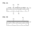
As illustrated in FIG. 1A, an insulating film 55 is formed over a substrate 51, and a first microcrystalline silicon film 57 which includes mixed phase grains 57 a including silicon crystallites and amorphous silicon is formed over the insulating film 55 using a plasma CVD method.
As the substrate 51, a glass substrate, a ceramic substrate, or the like can be used. Note that there is no limitation on the size of the substrate 51. For example, any of glass substrates of the 3rd to 10th generations which are often used in the field of the above flat panel displays can be used.
The insulating film 55 can be formed as a single layer or a stacked layer using a silicon nitride film or a silicon nitride oxide film by a CVD method, a sputtering method, or the like.
The first microcrystalline silicon film 57 has low density of mixed phase grains 57 a (the existing percentage of mixed phase grains in a plane) and high crystallinity of the mixed phase grains 57 a. Therefore, the first microcrystalline silicon film 57 may have a space 57 b between the adjacent mixed phase grains 57 a without the adjacent mixed phase grains 57 a being in contact with each other. The thickness of the first microcrystalline silicon film 57 is preferably greater than or equal to 1 nm and less than or equal to 10 nm. In a region having the space 57 b between the adjacent mixed phase grains 57 a without the adjacent mixed phase grains 57 a being in contact with each other, the smallest height of the mixed phase grains 57 a which are not in contact with each other is 1 nm or more and the largest height of the mixed phase grains 57 a which are not in contact with each other is 10 nm or less. Note that the mixed phase grains 57 a each include an amorphous silicon region and a plurality of crystallites that are microcrystals regarded as single crystals. In some cases, the mixed phase grains 57 a may include a twin crystal.
The first microcrystalline silicon film 57 is formed in a treatment chamber of a plasma CVD apparatus, using plasma generated by glow discharge with the use of a mixture of a deposition gas containing silicon and hydrogen as a source gas, under a first condition which allows mixed phase grains serving as nuclei to be formed in the state that the density of mixed phase grains is low and the crystallinity of the mixed phase grains is high. Alternatively, the first microcrystalline silicon film 57 is formed using plasma generated by glow discharge with the use of a mixture of a deposition gas containing silicon, hydrogen, and a rare gas such as helium, neon, argon, krypton, or xenon. Here, the microcrystalline silicon is formed under the first condition in which the deposition gas containing silicon is diluted with hydrogen by setting the flow rate of hydrogen at a flow rate greater than or equal to 50 times and less than or equal to 1000 times that of the deposition gas and the pressure inside the treatment chamber is set higher than or equal to 67 Pa and lower than or equal to 1333 Pa (higher than or equal to 0.5 Torr and lower than or equal to 10 Torr). The deposition temperature at this time is preferably from room temperature to 300° C., and further preferably 150° C. to 280° C. The distance between an upper electrode and a lower electrode of the plasma CVD apparatus may be set to a distance which allows generation of plasma. With the first condition, crystal growth is promoted and the crystallinity of the mixed phase grains 57 a is increased. That is, the size of the crystallites included in the mixed phase grains 57 a is increased. Further, the space 57 b is formed between the adjacent mixed phase grains 57 a, so that the density of mixed phase grains 57 a is lowered.
As typical examples of the deposition gas containing silicon, there are SiH4 and Si2H6.
In the case where a rare gas such as helium, argon, neon, krypton, or xenon is mixed into the source gas of the first microcrystalline silicon film 57, the deposition rate of the first microcrystalline silicon film 57 can be increased. Moreover, in the case where the deposition rate is increased, the amount of impurities mixed in the first microcrystalline silicon film 57 is reduced, so that the crystallinity of the first microcrystalline silicon film 57 can be improved.
In the glow discharge at the time of forming the first microcrystalline silicon film 57, the plasma is generated by application of high-frequency power with a frequency of 3 MHz to 30 MHz, typically, 13.56 MHz or 27.12 MHz in the HF band, or high-frequency power with a frequency of approximately 30 MHz to 300 MHz in the VHF band, typically 60 MHz. It is preferable to determine the power for generating the plasma as appropriate in accordance with the ratio of the flow rate of hydrogen to the flow rate of the deposition gas containing silicon.
Next, as illustrated in FIG. 1B, a second microcrystalline silicon film 59 is formed over the first microcrystalline silicon film 57. The second microcrystalline silicon film 59 is formed under a condition which allows the second microcrystalline silicon film 59 to fill the space 57 b between the mixed phase grains 57 a of the first microcrystalline silicon film 57 and also promotes crystal growth. Note that the thickness of the second microcrystalline silicon film 59 is preferably greater than or equal to 30 nm and less than or equal to 100 nm.
The second microcrystalline silicon film 59 is formed in a treatment chamber of the plasma CVD apparatus, using plasma generated by glow discharge with the use of a mixture of a deposition gas containing silicon and hydrogen as a source gas under a second condition. Alternatively, the second microcrystalline silicon film 59 may be formed using plasma generated by glow discharge with the use of a mixture of a deposition gas containing silicon, hydrogen, and a rare gas such as helium, neon, argon, krypton, or xenon under the second condition. Here, the microcrystalline silicon is formed under the second condition in which the deposition gas containing silicon is diluted with hydrogen by setting the flow rate of hydrogen at a flow rate greater than or equal to 100 times and less than or equal to 2000 times that of the deposition gas and the pressure inside the treatment chamber is set higher than or equal to 1333 Pa and lower than or equal to 13332 Pa (higher than or equal to 10 Torr and lower than or equal to 100 Torr). As a result, the ratio of a crystalline region to the amorphous semiconductor region is increased in the second microcrystalline silicon film 59, whereby the crystallinity is increased. The deposition temperature at this time is preferably from room temperature to 300° C., and further preferably 150° C. to 280° C. The distance between an upper electrode and a lower electrode of the plasma CVD apparatus is set to a distance which allows generation of plasma. By newly generating the mixed phase grains of the second microcrystalline silicon film in spaces between the mixed phase grains of the first microcrystalline silicon film, the size of the mixed phase grains is reduced. Therefore, it is preferable that the frequency of generation of the mixed phase grains of the second microcrystalline silicon film is lower than that of the mixed phase grains of the first microcrystalline silicon film.
In the case where a rare gas such as helium, argon, neon, krypton, or xenon is mixed into the source gas of the second microcrystalline silicon film 59, the crystallinity of the second microcrystalline silicon film 59 can be improved in a manner similar to that of the first microcrystalline silicon film 57.
The condition for generating plasma by glow discharge at the time of forming the first microcrystalline silicon film 57 can be employed as appropriate for the second microcrystalline silicon film 59. In the case where the condition for generating plasma by glow discharge at the time of forming the first microcrystalline silicon film 57 and that at the time of forming the second microcrystalline silicon film 59 are the same, throughput can be increased; however, they may be different from each other.
Since the density of mixed phase grains in the microcrystalline silicon film depends on the density of the mixed phase grains 57 a in the first microcrystalline silicon film 57, the density of the mixed phase grains 57 a in the first microcrystalline silicon film 57 is preferably more than or equal to 100/μm2 and less than or equal to 10000/μm2, and further preferably more than or equal to 500/μm2 and less than or equal to 2500/μm2. When the density of the mixed phase grains 57 a in the first microcrystalline silicon film 57 is within the above-described range, the density of the mixed phase gains 57 a is low and the mixed phase grains 57 a are dispersed; accordingly, the size of the mixed phase grains of the microcrystalline silicon film can be increased.
In this embodiment, by stacking the first microcrystalline silicon film 57 and the second microcrystalline silicon film 59, the microcrystalline silicon film having high crystallinity in which there is no space between the mixed phase grains can be formed. Note that the second microcrystalline silicon film 59 is a film which has low adhesiveness to the insulating film 55 and has a high field-effect mobility as compared to the first microcrystalline silicon film 57. The density of the microcrystalline silicon film is higher than 1.9 g/cm3 and lower than or equal to 2.3 g/cm3, which is closer to the density of normal single crystal silicon (2.35 g/cm3); thus, the mixed phase grains are densely packed in the microcrystalline silicon film. The resistivity of the microcrystalline silicon film is higher than or equal to 1.0×10⁵ Ω·cm and lower than or equal to 1.0×10⁸ Ω·cm, preferably higher than or equal to 5×10⁶ Ω·cm and lower than or equal to 5.0×10⁷ Ω·cm. The activation energy of conductivity of the microcrystalline silicon film in the state where voltage is not applied is 0.5 eV to 0.6 eV and the microcrystalline silicon film is an i-type semiconductor.
The first microcrystalline silicon film 57 and the second microcrystalline silicon film 59 are formed of microcrystalline silicon. Note that microcrystalline silicon is a semiconductor having an intermediate structure between an amorphous structure and a crystalline structure (including single crystal and polycrystal). Microcrystalline silicon is a semiconductor having a third state that is stable in terms of free energy and is a crystalline semiconductor having short-range order and lattice distortion, in which columnar or needle-like mixed phase grains having a grain size of 2 nm to 200 nm, preferably 10 nm to 80 nm, further preferably 20 nm to 50 nm, still further preferably 25 nm to 33 nm have grown in a direction normal to the substrate surface. Therefore, there is a case in which a crystal grain boundary is formed at the interface between the columnar or needle-like mixed phase grains. Note that the grain size of a mixed phase grain here means a maximum diameter of a mixed phase grain in a plane parallel to the substrate surface.
The Raman spectrum of microcrystalline silicon is shifted to a smaller wavenumber region than 520 cm−1 which represents single crystal silicon. That is, the peak of the Raman spectrum of the microcrystalline silicon exists between 520 cm−1 which represents single crystal silicon and 480 cm−1 which represents amorphous silicon. Microcrystalline silicon includes at least 1 at. % or more of hydrogen or halogen to terminate a dangling bond. Moreover, the microcrystalline silicon may contain a rare gas element such as helium, argon, krypton, or neon to further promote lattice distortion, so that stability is increased and favorable microcrystalline silicon can be obtained. Such microcrystalline silicon is disclosed in, for example, U.S. Pat. No. 4,409,134.
In this embodiment, by reducing spaces between mixed phase grains, a microcrystalline silicon film having high crystallinity can be formed.
(Embodiment 2)
In this embodiment, a manufacturing method of a microcrystalline silicon film having higher crystallinity than the microcrystalline silicon film of Embodiment 1 will be described with reference to FIGS. 1A and 1B and FIG. 2.
In a manner similar to that of Embodiment 1, a first microcrystalline silicon film 57 and a second microcrystalline silicon film 59 are formed through the process of FIGS. 1A and 1B.
Next, as illustrated in FIG. 2, a third microcrystalline silicon film 61 is formed over the second microcrystalline silicon film 59.
The third microcrystalline silicon film 61 is formed in a treatment chamber of the plasma CVD apparatus, using plasma generated by glow discharge with the use of a mixture of a deposition gas containing silicon and hydrogen as a source gas under a third condition. Alternatively, the third microcrystalline silicon film 61 may be formed using plasma generated by glow discharge with the use of a mixture of a deposition gas containing silicon, hydrogen, and a rare gas such as helium, neon, argon, krypton, or xenon as a source gas under the third condition. Here, the third microcrystalline silicon film is formed under the third condition in which the deposition gas containing silicon is diluted with hydrogen by setting the ratio of the flow rate of hydrogen to the flow rate of the deposition gas at a ratio higher than that in the second condition and the pressure inside the treatment chamber is set higher than or equal to 1333 Pa and lower than or equal to 13332 Pa (higher than or equal to 10 Torr and lower than or equal to 100 Torr) in a manner similar to that of the second condition. The deposition temperature at this time is preferably from room temperature to 300° C., and further preferably 150° C. to 280° C.
By setting the ratio of the flow rate of hydrogen to the flow rate of the deposition gas containing silicon at a ratio higher than that in the second condition, the crystallinity of the third microcrystalline silicon film 61 can be further increased, and a microcrystalline silicon film whose surface crystallinity is higher than that of the microcrystalline silicon film in Embodiment 1 can be formed.
(Embodiment 3)
In this embodiment, a manufacturing method of a thin film transistor formed in a semiconductor device that is an embodiment of the present invention will be described with reference to FIGS. 3A to 3D, FIGS. 4A and 4B, and FIGS. 5A to 5C. Note that an n-channel thin film transistor has higher carrier mobility than a p-channel thin film transistor. In this embodiment, a manufacturing method of an n-channel thin film transistor will be described.
As illustrated in FIG. 3A, a gate electrode 103 is formed over a substrate 101. Then, a gate insulating film 105 which covers the gate electrode 103 (also referred to as a first gate electrode) is formed. A first microcrystalline silicon film 107 is formed over the gate insulating film 105.
As the substrate 101, the substrate 51 described in Embodiment 1 can be used as appropriate.
The gate electrode 103 can be formed in the following manner: a conductive film is formed over the substrate 101 by a sputtering method or a vacuum evaporation method using the any metal material of Mo, Ti, Cr, Ta, W, Al, Cu, Nd, Sc, or Ni; a mask is formed over the conductive film by a photolithography method; and the conductive film is etched using the mask. In order to improve adhesion between the gate electrode 103 and the substrate 101, a nitride film of any of the above-described metal materials may be provided between the substrate 101 and the gate electrode 103. In this embodiment, a conductive film is formed over the substrate 101 and etched using a resist mask formed by a photolithography method.
Note that side surfaces of the gate electrode 103 are preferably tapered. This is because an insulating film, a silicon film, and a wiring formed over the gate electrode 103 in later steps can be prevented from being cut at a step portion of the gate electrode 103. In order to taper the side surfaces of the gate electrode 103, etching may be performed while the resist mask is made to recede.
The gate insulating film 105 can be formed using the insulating film 55 described in Embodiment 1 as appropriate.
The gate insulating film 105 can be formed by a CVD method, a sputtering method, or the like.
Note that in the case where the gate insulating film 105 is formed using a silicon nitride film or a silicon nitride oxide film, the threshold voltage of the thin film transistor shifts in the negative direction; therefore, oxygen plasma treatment in which a surface of the gate insulating film 105 is exposed to plasma of an oxidizing gas atmosphere may be performed. The oxidizing gas atmosphere is an atmosphere containing at least one of oxygen, ozone, dinitrogen monoxide, or the like. By the oxygen plasma treatment, a normally-off transistor can be manufactured.
The first microcrystalline silicon film 107 can be formed under a first condition which allows the density of mixed phase grains to be low and the crystallinity of the mixed phase grains to be high, in a manner similar to that of the first microcrystalline silicon film 57 described in Embodiment 1.
In the case where a rare gas such as helium, argon, neon, krypton, or xenon is mixed into the source gas of the first microcrystalline silicon film 107, the crystallinity of the first microcrystalline silicon film 107 can be increased. Accordingly, the on-state current and the field-effect mobility of the thin film transistor are increased and the throughput of the thin film transistor can also be increased.
Next, as illustrated in FIG. 3B, a second microcrystalline silicon film 109 is formed over the first microcrystalline silicon film 107. The second microcrystalline silicon film 109 can be formed under a second condition which allows the second microcrystalline silicon film 109 to fill the space between the mixed phase grains of the first microcrystalline silicon film 107 and also promotes crystal growth, in a manner similar to that of the second microcrystalline silicon film 59 described in Embodiment 1.
In the case where a rare gas such as helium, argon, neon, krypton, or xenon is mixed into the source gas of the second microcrystalline silicon film 109, the crystallinity of the second microcrystalline silicon film 109 can be increased in a manner similar to that of the first microcrystalline silicon film 107. Accordingly, the on-state current and the field-effect mobility of the thin film transistor are increased and the throughput of the thin film transistor can also be increased.
Next, as illustrated in FIG. 3C, a silicon film 111 is formed over the second microcrystalline silicon film 109. The silicon film 111 includes a microcrystalline silicon region 111 a and an amorphous silicon region 111 b. Then, an impurity silicon film 113 is formed over the silicon film 111, and a resist mask 115 is formed over the impurity silicon film 113.
The silicon film 111 including the microcrystalline silicon region 111 a and the amorphous silicon region 111 b can be formed under a condition which causes partial crystal growth using the second microcrystalline silicon film 109 as a seed crystal (a condition by which the crystal growth is reduced).
The silicon film 111 is formed in a treatment chamber of the plasma CVD apparatus, using plasma generated by glow discharge with the use of a mixture of a deposition gas containing silicon, hydrogen, and a gas containing nitrogen. As examples of the gas containing nitrogen, there are ammonia, nitrogen, nitrogen fluoride, nitrogen chloride, and the like. Generation of plasma by glow discharge can be performed in a manner similar to that of the first microcrystalline silicon film 107.
In that case, the ratio of the flow rate of hydrogen to the flow rate of the deposition gas containing silicon is set to a ratio for forming a microcrystalline silicon film in a manner similar to that in forming the first microcrystalline silicon film 107 or the second microcrystalline silicon film 109, and the gas containing nitrogen is used as a source gas, whereby the degree of crystal growth can be reduced as compared to those under the deposition conditions for the first microcrystalline silicon film 107 and the second microcrystalline silicon film 109. Specifically, at an early stage of deposition of the silicon film 111, the gas containing nitrogen included in the source gas partly suppresses the crystal growth, so that a conical microcrystalline silicon region or a pyramidal microcrystalline silicon region grows and an amorphous silicon region is formed. Further, at a middle stage or a later stage of the deposition, crystal growth of the conical or pyramidal microcrystalline silicon region stops, and only an amorphous silicon region is deposited. Accordingly, in the silicon film 111, the microcrystalline silicon region 111 a and the amorphous semiconductor region 111 b which is formed using a well-ordered silicon film having fewer defects and a steep tail of a level at a valence band edge, can be formed.
Here, a typical example of a condition for forming the silicon film 111 is as follows: the flow rate of hydrogen is 10 times to 2000 times, preferably 10 times to 200 times that of the deposition gas containing silicon. Note that in a typical example of a condition for forming a normal amorphous silicon film, the flow rate of hydrogen is 0 times to 5 times that of the deposition gas containing silicon.
In the case where a rare gas such as helium, neon, argon, xenon, or krypton is introduced into the source gas of the silicon film 111, the deposition rate can be increased.
It is preferable for the silicon film 111 to have a thickness of 50 nm to 350 nm, and further preferable for the silicon film 111 to have a thickness of 120 nm to 250 nm.
FIGS. 4A and 4B are enlarged views of the portion between the gate insulating film 105 and the impurity silicon film 113 illustrated in FIG. 3C.
As illustrated in FIG. 4A, the microcrystalline silicon region 111 a in the silicon film 111 has a projection and a depression; and the projection has a conical or pyramidal shape whose width decreases from the gate insulating film 105 side toward the amorphous silicon region 111 b side (a tip of the projection has an acute angle). Alternatively, the microcrystalline silicon region 111 a may have a projecting (inverted conical or pyramidal) shape whose width increases from the gate insulating film 105 side toward the amorphous semiconductor region 111 b side.
By setting the thickness of the first microcrystalline silicon film 107, the second microcrystalline silicon film 109, and the microcrystalline silicon region 111 a, that is, the distance from the interface between the first microcrystalline silicon film 107 and the gate insulating film 105 to the tip of the projection of the microcrystalline silicon region 111 a to 5 nm or more and 310 nm or less, the off-state current of the thin film transistor can be reduced.
Further, in order to improve the crystallinity of the microcrystalline silicon region 111 a, it is preferable that the concentration of oxygen contained in the silicon film 111, which is measured by secondary ion mass spectrometry, be less than 1×10¹⁸ atoms/cm3. The nitrogen concentration profile of the semiconductor film 111 that is measured by secondary ion mass spectrometry has a peak concentration greater than or equal to 1×10²⁰ atoms/cm3 and less than or equal to 1×10²¹ atoms/cm3, preferably greater than or equal to 2×10²⁰ atoms/cm3 and less than or equal to 1×10²¹ atoms/cm3.
The amorphous silicon region 111 b is formed of an amorphous semiconductor containing nitrogen. The nitrogen of the amorphous semiconductor containing nitrogen may exist, for example, as an NH group or an NH2 group. As the amorphous semiconductor, amorphous silicon can be used.
Amorphous silicon containing nitrogen is a semiconductor having lower energy at an Urbach edge that is measured by a constant photocurrent method (CPM) or photoluminescence spectroscopy and a smaller amount of defect absorption spectrum, as compared to a conventional amorphous semiconductor. In other words, as compared to the conventional amorphous semiconductor, the amorphous silicon containing nitrogen is a well-ordered semiconductor which has few defects and whose tail of a level at a valence band edge is steep. Since the amorphous silicon containing nitrogen has a steep tail of a level at a valence band edge, the band gap is wide and tunnel current does not flow easily. Therefore, when the amorphous silicon containing nitrogen is provided between the microcrystalline silicon region 111 a and the impurity silicon film 113, the off-state current of the thin film transistor can be reduced. In addition, by provision of the amorphous silicon containing nitrogen, the on-state current and the field-effect mobility can be increased.
Further, the peak region of a spectrum of the amorphous silicon containing nitrogen that is measured by low-temperature photoluminescence spectroscopy is higher than or equal to 1.31 eV and lower than or equal to 1.39 eV. Note that the peak region of a spectrum of microcrystalline silicon, which is measured by low-temperature photoluminescence spectroscopy is higher than or equal to 0.98 eV and lower than or equal to 1.02 eV. Accordingly, the amorphous silicon containing nitrogen is different from microcrystalline silicon.
The microcrystalline silicon region 111 a, as well as the amorphous silicon region 111 b, may include a NH group or an NH2 group.
Further, as illustrated in FIG. 4B, a silicon crystal grain 111 c whose grain size is greater than or equal to 1 nm and less than or equal to 10 nm, preferably greater than or equal to 1 nm and less than or equal to 5 nm may be included in the amorphous silicon region 111 b, so that the on-state current and the filed-effect mobility can be further increased.
The microcrystalline silicon having a projecting (conical or pyramidal) shape whose width decreases from the gate insulating film 105 toward the amorphous silicon region 111 b is formed in the following manner: after the second microcrystalline silicon film is formed under the deposition condition for microcrystalline silicon, crystal growth is caused on such a condition that the crystal growth is reduced, and amorphous silicon is deposited.
Since the microcrystalline silicon region 111 a in the silicon film 111 has the conical or pyramidal shape or the inverted conical or pyramidal shape, resistance in a vertical direction (film thickness direction) of when voltage is applied between a source and drain electrodes in an on state, i.e., the resistance of the silicon film 111 can be lowered. Further, tunnel current does not easily flow since amorphous silicon containing nitrogen is provided between the microcrystalline silicon region 111 a and the impurity silicon film 113. Amorphous silicon containing nitrogen is a well-ordered semiconductor having few defects and a steep tail of a level at a valence band edge. Thus, in the thin film transistor described in this embodiment, the on-state current and the field-effect mobility can be increased and the off-state current can be reduced.
The impurity silicon film 113 is formed using amorphous silicon to which phosphorus is added, microcrystalline silicon to which phosphorus is added, or the like. A structure in which amorphous silicon to which phosphorus is added and microcrystalline silicon to which phosphorus is added are stacked can also be employed. In the case of forming a p-channel thin film transistor as a thin film transistor, the impurity silicon film 113 is formed using microcrystalline silicon to which boron is added, amorphous silicon to which boron is added, or the like.
The impurity silicon film 113 is formed in a treatment chamber of the plasma CVD apparatus, using plasma generated by glow discharge with the use of a mixture of a deposition gas containing silicon, hydrogen, and phosphine (diluted with hydrogen or silane) as a source gas. The deposition gas containing silicon is diluted with hydrogen, in formation of amorphous silicon to which phosphorus is added or microcrystalline silicon to which phosphorus is added. In the case of manufacturing a p-type thin film transistor, the impurity silicon film 113 may be formed using plasma generated by glow discharge using diborane instead of phosphine.
The resist mask 115 can be formed by a photolithography step.
Next, as illustrated in FIG. 3D, the first microcrystalline silicon film 107, the second microcrystalline silicon film 109, the silicon film 111, and the impurity silicon film 113 are etched using the resist mask 115. By this step, the first microcrystalline silicon film 107, the second microcrystalline silicon film 109, the silicon film 111, and the impurity silicon film 113 are divided into elements, so that a silicon stacked body 117 and an impurity silicon film 121 are formed. The silicon stacked body 117 is formed including part of the first microcrystalline silicon film 107, part of the second microcrystalline silicon film 109, and part of the silicon film 111. The silicon stacked body 117 is constituted of a microcrystalline silicon region 117 a which includes part of the first microcrystalline silicon film 107, part of the second microcrystalline silicon film 109, and part of the microcrystalline silicon region of the silicon film 111 and an amorphous silicon region 117 b which includes part of the amorphous silicon region of the silicon film 111. Then, the resist mask 115 is removed.
Then, as illustrated in FIG. 5A, a conductive film 127 is formed over the impurity silicon film 121. The conductive film 127 is formed by a CVD method, a sputtering method, or a vacuum evaporation method.
Next, as illustrated in FIG. 5B, wirings 129 a and 129 b functioning as a source electrode and a drain electrode are formed by forming a resist mask (not illustrated) by a photolithography step and etching the conductive film 127 with the use of the resist mask. The etching of the conductive film 127 may be either dry etching or wet etching. Note that one of the wirings 129 a and 129 b functions as a signal line as well as a source electrode or a drain electrode. However, without limitation thereto, a signal line may be provided separately from the source and drain electrodes.
Next, the impurity silicon film 121 and the silicon stacked body 117 are partly etched, so that a pair of impurity silicon films 131 a and 131 b functioning as a source and drain regions are formed. A silicon stacked body 133 including a microcrystalline silicon region 133 a and a pair of amorphous silicon regions 133 b is formed. At this time, the silicon stacked body 117 is etched so as to expose the microcrystalline silicon region 133 a, so that the silicon stacked body 133 is formed in which the microcrystalline silicon region 133 a and the amorphous silicon regions 133 b are stacked in regions covered with the wirings 129 a and 129 b and the microcrystalline silicon region 133 a is exposed in a region not covered with the wirings 129 a and 129 b and overlapping with the gate electrode.
Next, dry etching may be performed. As the condition for the dry etching, a condition by which the exposed microcrystalline silicon region 133 a and the exposed amorphous silicon regions 133 b are not damaged and in which the etching rate of the microcrystalline silicon region 133 a and the amorphous silicon regions 133 b is low is used. That is, a condition by which surfaces of the exposed microcrystalline silicon region 133 a and the exposed amorphous silicon regions 133 b are hardly damaged and by which the thicknesses of the exposed microcrystalline silicon region 133 a and the exposed amorphous silicon regions 133 b are hardly reduced is used. As an etching gas, Cl2, CF4, N2, or the like is typically used.
Then, plasma treatment may be performed on the surfaces of the microcrystalline silicon region 133 a and the amorphous silicon regions 133 b. By the plasma treatment, impurities such as a residue existing on the exposed microcrystalline silicon region 133 a and the exposed amorphous silicon regions 133 b can be removed and defects of the microcrystalline silicon region 133 a can be reduced. Further by the plasma treatment, insulation between the source region and the drain region can be ensured, and thus, in a completed thin film transistor, off-state current can be reduced, and variation in electric characteristics can be reduced.
Through the above-described process, a single-gate thin film transistor can be manufactured. A single-gate thin film transistor with low off-state current, high on-state current, and high field-effect mobility can be manufactured with high productivity. Note that in this embodiment, a thin film transistor whose gate electrode is located below a channel region has been described as a semiconductor device according to an embodiment of the present invention; however, the present invention may also be applied to a dual-gate thin film transistor whose back gate electrode is located above a channel region as a semiconductor device according to an embodiment of the present invention.
Next, an insulating film 137 is formed over the silicon stacked body 133 and the wirings 129 a and 129 b. The insulating film 137 can be formed in a manner similar to that for the gate insulating film 105.
Next, an opening (not illustrated) is formed in the insulating film 137 with the use of a resist mask formed by a photolithography step. A back gate electrode 139 is formed over the insulating film 137 (see FIG. 5C). Through the above-described process, a dual-gate thin film transistor can be manufactured.
The back gate electrode 139 can be formed in a manner similar to that of the wirings 129 a and 129 b. Alternatively, the back gate electrode 139 can be formed using a light-transmitting conductive material.
The back gate electrode 139 can be formed in parallel to the gate electrode 103. In this case, each of potential applied to the back gate electrode 139 and potential applied to the gate electrode 103 can be controlled independently. Thus, the threshold voltage of the thin film transistor can be controlled. Further, regions in which carriers flow, that is, channel regions, are formed on the gate insulating film 105 side and on the insulating film 137 side in the microcrystalline silicon region; thus, the on-state current of the thin film transistor can be increased.
The back gate electrode 139 can be connected to the gate electrode 103. That is, the gate electrode 103 and the back gate electrode 139 can be connected through an opening (not illustrated) formed in the gate insulating film 105 and the insulating film 137. In this case, potential applied to the back gate electrode 139 and potential applied to the gate electrode 103 are equal. As a result, in the silicon film, regions in which carriers flow, that is, channel regions are formed on the gate insulating film 105 side and on the insulating film 137 side in the microcrystalline silicon region; thus, the on-state current of the thin film transistor can be increased.
Further alternatively, the back gate electrode 139 is not necessarily connected to the gate electrode 103 and may be in a floating state. In that case, channel regions are formed on the gate insulating film 105 side and on the insulating film 137 side in the microcrystalline silicon region without a potential applied to the back gate electrode 139; thus, the on-state current of the thin film transistor can be increased.
Further, the back gate electrode 139 may overlap with the wirings 129 a and 129 b with the insulating film 137 provided therebetween.
Through the above-described process, a single-gate thin film transistor and a dual-gate thin film transistor having high on-state current, high field-effect mobility, and low off-state current can be manufactured. In the case where, after exposing a gate insulating film to oxygen plasma, an i-type microcrystalline silicon film having an activation energy of 0.5 eV to 0.6 eV is formed for a channel region as in Embodiment 1, a thin film transistor which is normally off as well as having the above-described effects can be manufactured.
(Embodiment 4)
In this embodiment, a manufacturing method of a thin film transistor formed in the semiconductor device that is an embodiment of the present invention will be described with reference to FIG. 6. FIG. 6 corresponds to the step illustrated in FIG. 5B.
In a manner similar to that of Embodiment 3, a conductive film 127 is formed through the process of FIGS. 3A to 3D and FIG. 5A.
Then, as illustrated in FIG. 6, wirings 129 a and 129 b are formed and an impurity silicon film 121 and a silicon stacked body 117 are partly etched, so that a pair of impurity silicon films 131 a and 131 b serving as a source region and a drain region are formed in a manner similar to that of Embodiment 3. A silicon stacked body 143 including a microcrystalline silicon region 143 a and an amorphous silicon region 143 b is formed. At this time, the silicon stacked body 117 is etched so as to expose the amorphous region 143 b, so that the silicon stacked body 143 is formed in which the microcrystalline silicon region 143 a and the amorphous silicon region 143 b are stacked in regions covered with the wirings 129 a and 129 b and the microcrystalline silicon region 143 a is not exposed and the amorphous silicon region 143 b is exposed in a region not covered with the wirings 129 a and 129 b and overlapping with the gate electrode. Note that the etching amount of the silicon stacked body 117 is smaller than that in the case of FIG. 5B.
A later process is similar to that of Embodiment 3. Through the above-described process, a single-gate thin film transistor can be manufactured. Since the back channel side of the thin film transistor is amorphous, the off-state current can be reduced as compared to the thin film transistor illustrated in FIG. 5B.
Further in this embodiment, after the step illustrated in FIG. 6, a back gate electrode 139 may be formed over an insulating film 137 as in the step illustrated in FIG. 5C.
EXAMPLE Example 1
In this example, electric characteristics of the following thin film transistors will be described: a thin film transistor whose microcrystalline silicon film is formed under only the first condition described in Embodiment 1 (Sample 1), a thin film transistor whose microcrystalline silicon film is formed under only the second condition described in Embodiment 1 (Sample 2), and a thin film transistor in which a first microcrystalline silicon film formed under the first condition and a second microcrystalline silicon film formed under the second condition are stacked (Sample 3).
A manufacturing method of the thin film transistors of this example will be described with reference to FIGS. 3A to 3D and FIGS. 5A to 5C.
First, a base insulating film (not illustrated here) was formed over a substrate 101, and a gate electrode 103 was formed over the base insulating film.
Here, a glass substrate (EAGLE XG manufactured by Corning Incorporated) was used as the substrate 101.
The gate electrode 103 had a structure in which an aluminum layer was sandwiched between titanium layers. Specifically, first, a first titanium film with a thickness of 50 nm was formed over the base insulating film by sputtering a titanium target with argon ions. At this time, the flow rate of argon which was introduced into a treatment chamber was 20 sccm and the pressure inside the treatment chamber was set at 0.1 Pa. Then, an aluminum target was sputtered with argon ions, so that an aluminum film with a thickness of 100 nm was formed. At this time, the flow rate of argon which was introduced into the treatment chamber was 50 sccm and the pressure inside the treatment chamber was set at 0.4 Pa. Furthermore, a titanium target was sputtered with argon ions, so that a second titanium film with a thickness of 120 nm was formed. At this time, the flow rate of argon which was introduced into the treatment chamber was 20 sccm and the pressure inside the treatment chamber was set at 0.1 Pa.
After that, a resist was applied over the second titanium film and was irradiated with light with the use of a first photomask and developed to form a resist mask.
Next, etching was performed using the resist mask, so that the gate electrode 103 was formed. Here, two-step etching was conducted using an inductively coupled plasma (ICP) apparatus in the following manner. The first etching was performed under a condition where the ICP power was 600 W, the bias power was 250 W, boron trichloride was introduced at a flow rate of. 60 sccm and chlorine was introduced at a flow rate of 20 sccm as an etching gas, and the pressure inside a treatment chamber was 1.2 Pa. After that, the second etching was performed under a condition where the ICP power was 500 W, the bias power was 50 W, the pressure was 2.0 Pa, carbon fluoride was introduced at a flow rate of 80 sccm as an etching gas, and the pressure inside the treatment chamber was 2.0 Pa. After that, the resist mask was removed.
Next, a gate insulating film 105 was formed over the gate electrode 103 and the base insulating film.
The gate insulating film 105 was formed using a silicon nitride film. The silicon nitride film was formed with a thickness of 300 nm by a plasma CVD method.
The silicon nitride film was formed by plasma discharge performed under the following condition: silane, hydrogen, nitrogen, and ammonia were introduced as a source gas at flow rates of 15 sccm, 200 sccm, 180 sccm, and 500 sccm; the pressure of a treatment chamber was 100 Pa; the substrate temperature was 250° C.; the RF power source frequency was 13.56 MHz; and power of an RF power source was 200 W.
Next, plasma treatment was performed on the gate insulating film 105. Here, plasma treatment for Sample 1 was performed at 300 W under a condition in which hydrogen was introduced at a flow rate of 400 sccm and the pressure inside a treatment chamber was stabilized at 60 Pa. Then, dinitrogen monoxide (N2O) was introduced at a flow rate of 400 sccm and the pressure inside the treatment chamber was stabilized at 60 Pa, and plasma discharge was performed at 300 W. Plasma treatment for Sample 2 and Sample 3 was performed by plasma discharge at 300 W under a condition in which dinitrogen monoxide was introduced at a flow rate of 400 sccm and the pressure inside a treatment chamber was stabilized at 60 Pa. Note that the above-described plasma treatment was performed using a parallel-plate plasma apparatus, with the upper electrode temperature and the lower electrode temperature set at 250° C. and 290° C. respectively.
Next, a microcrystalline silicon film was formed over the gate insulating film 105.
Here, as the microcrystalline silicon film of Sample 1, a microcrystalline silicon film with a thickness of 30 nm was formed under only the first condition. For Sample 2, a microcrystalline silicon film with a thickness of 30 nm was formed under only the second condition. Further for Sample 3, after forming a first microcrystalline silicon film with a thickness of 5 nm under the first condition, a second microcrystalline silicon film with a thickness of 85 nm was formed under the second condition.
The first condition for depositing the microcrystalline silicon film was a condition in which plasma discharge was performed in a plasma CVD method by introducing silane, hydrogen, and argon as a source gas at flow rates of 4 sccm, 750 sccm, and 750 sccm respectively, and setting the pressure inside a treatment chamber at 532 Pa, the RF power source frequency at 13.56 MHz, and the power of the RF power at 150 W. Note that here, the microcrystalline silicon film was deposited using a parallel-plate plasma apparatus, with the upper electrode temperature and the lower electrode temperature set at 250° C. and 290° C. respectively.
The second condition for depositing the microcrystalline silicon film was a condition in which plasma discharge was performed in a plasma CVD method by introducing silane, hydrogen, and argon as a source gas at flow rates of 1.8 sccm, 750 sccm, and 750 sccm respectively, and setting the pressure inside a treatment chamber at 5000 Pa and the RF power source frequency at 13.56 MHz.
Next, a silicon film 111 was formed over the microcrystalline silicon film, and an impurity silicon film 113 was formed over the silicon film 111. The silicon film 111 and the impurity silicon film 113 were stacked by a plasma CVD method.
As the deposition condition of the silicon film 111 for Sample 1 and Sample 2, the thickness of the silicon film 111 was 175 nm. In Sample 3, a silicon film with a thickness of 80 nm was formed. The deposition condition at this time was a condition in which plasma discharge was performed by introducing silane, 1000 ppm ammonia (diluted with hydrogen), hydrogen, and argon as a source gas at flow rates of 20 sccm, 50 sccm, 700 sccm, and 750 sccm respectively, and setting the pressure inside a treatment chamber at 350 Pa, the RF power source frequency at 13.56 MHz, and the power of the RF power at 60 W. Note that here, the silicon film 111 was deposited using the parallel-plate plasma apparatus, with the upper electrode temperature and the lower electrode temperature set at 250° C. and 290° C. respectively.
As the impurity silicon film 113, an amorphous silicon film with a thickness of 50 nm to which phosphorus was added was formed. The deposition condition at this time was a condition in which plasma discharge was performed by introducing silane, 0.5% phosphine (diluted with hydrogen), and hydrogen as a source gas at flow rates of 20 sccm, 170 sccm, and 100 sccm respectively, and setting the pressure inside a treatment chamber at 170 Pa, the RF power source frequency at 13.56 MHz, and the power of the RF power at 60 W. Note that here, the impurity silicon film was deposited using the parallel-plate plasma apparatus, with the upper electrode temperature and the lower electrode temperature set at 250° C. and 290° C. respectively.
Next, a resist was applied over the impurity silicon film 113 and was irradiated with light with the use of a second photomask and developed to form a resist mask 115. The state at this time is illustrated in FIG. 3C.
Next, the microcrystalline silicon film, the silicon film 111, and the impurity silicon film 113 were etched with the use of the resist mask 115, so that a silicon stacked body 117 including a microcrystalline silicon region 117 a and an amorphous silicon region 117 b, and an impurity silicon film 121 were formed.
Here, the etching was performed using an ICP apparatus under a condition in which the ICP power was 1000 W, the bias power was 80 W, chlorine was introduced as an etching gas at a flow rate of 100 sccm, and the pressure inside a treatment chamber was 1.51 Pa. After that, the resist mask 115 was removed (see FIG. 3D).
Next, as illustrated in FIG. 5A, a conductive film 127 was formed over the gate insulating film 105 so as to cover the silicon stacked body 117 and the impurity silicon film 121.
Here, the conductive film 127 had a structure in which an aluminum layer was sandwiched between titanium layers and was formed in a manner similar to that of the gate electrode 103. Note that the thicknesses of the first titanium film, the aluminum film, and the second titanium film were 50 nm, 200 nm, and 50 nm, respectively.
Next, a resist was applied over the conductive film 127 and was irradiated with light with the use of a third photomask and developed to form a resist mask (not illustrated). Dry etching was performed on the conductive film 127 with the use of the resist mask, so that wirings 129 a and 129 b were formed. Then, the impurity silicon film 121 was dry etched, so that a pair of impurity silicon films 131 a and 131 b serving as a source region and a drain region were formed. Further, the silicon stacked body 117 was partly etched, so that a silicon stacked body 133 including a microcrystalline silicon region 133 a and a pair of amorphous silicon regions 133 b was formed.
Here, the etching was performed using an ICP apparatus under a condition in which the ICP power was 450 W, the bias power was 100 W, boron chloride and chlorine were introduced as an etching gas at flow rates of 60 sccm and 100 sccm, respectively, and the pressure inside a treatment chamber was 1.9 Pa.
Note that the silicon stacked body 117 was etched 20 nm to 40 nm deep from its surface in Sample 1 and Sample 2, while the silicon stacked body 117 was etched 100 nm to 120 nm deep from its surface in Sample 3. Note that in this example, the planar shape of the wirings 129 a and 129 b functioning as the source electrode and drain electrode was linear.
Next, the surface of the silicon stacked body 133 was subjected to plasma treatment with carbon fluoride plasma, whereby impurities remaining on the surface of the silicon stacked body 133 were removed. Here, the plasma treatment was performed using the ICP apparatus under a condition in which the ICP power was 1000 W, the bias power was 0 W, carbon fluoride was introduced at a flow rate of 100 sccm, and the pressure inside a treatment chamber was 0.67 Pa.
Next in Sample 3, the surface of the silicon stacked body 133 was irradiated with water plasma, so that surface defects of the silicon stacked body 133 were reduced and the insulation properties of the source and drain regions were improved. Here, the silicon stacked body 133 was irradiated with plasma generated by introduction of water vapor at a flow rate of 300 sccm at an ICP power of 1800 W and a pressure of 66.5 Pa.
After that, the resist mask was removed. The state at this time of Sample 1 and Sample 2 is illustrated in FIG. 6, and that of Sample 3 is illustrated in FIG. 5B.
Next, a silicon nitride film with a thickness of 300 nm was formed as the insulating film 137. The deposition condition at this time was a condition in which plasma discharge was performed by introducing silane, ammonia, nitrogen, and hydrogen as a source gas at flow rates of 20 sccm, 220 sccm, 450 sccm, and 450 sccm respectively, and setting the pressure inside a treatment chamber at 160 Pa, the substrate temperature at 250° C., the RF power source frequency at 13.56 MHz, and the power of the RF power at 200 W.
Next, a resist was applied over the insulating film 137 and was irradiated with light with the use of a fourth photomask and developed to form a resist mask (not illustrated). With the use of the resist mask, part of the insulating film was dry etched so that the wirings 129 a and 129 b functioning as the source and drain electrodes were exposed. In addition, part of the insulating film 137 and part of the gate insulating film 105 were dry etched so that the gate electrode 103 was exposed. After that, the resist mask was removed.
Through the above-described process, Sample 1 and Sample 2 were manufactured.
Next, a conductive film was formed over the insulating film 137. After that, a resist was applied over the conductive film and was irradiated with light with the use of a fifth photomask and developed to form a resist mask (not illustrated). With the use of the resist mask, part of the conductive film was wet etched, so that a back gate electrode 139 was formed.
In this example, as the conductive film, a 50-nm-thick indium tin oxide was deposited by a sputtering method, and was subjected to wet-etching treatment, so that the back gate electrode 139 was formed. Although not illustrated, the back gate electrode 139 was connected to the gate electrode 103. After that, the resist mask was removed.
Through the above-described process, a dual-gate thin film transistor of Sample 3 was manufactured (see FIG. 5C).
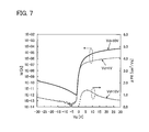
The measured electric characteristics of the thin film transistor of Sample 3 are shown in FIG. 7. In FIG. 7, Vg is the voltage applied to the gate electrode 103. From FIG. 7, it is found that a thin film transistor having high on-state current, high field-effect mobility, and low off-state current was able to be manufactured in this example.
Next, the average value (μFE_ave) of field-effect mobilities on sixteen points and the standard deviation for each of Samples 1 to 3 are shown in Table 1.
TABLE 1
μFE_ave Standard
(cm2/Vs) deviation
Sample
1 0.22 0.01
Sample 2 0.30 0.15
Sample 3 0.88 0.02
From Table 1, it can be noticed that the variation in field-effect mobility of Sample 3 is smaller than that of Sample 2. Therefore, the variation in electric characteristics of a thin film transistor can be reduced by forming a first microcrystalline silicon film under the first condition and then stacking a second microcrystalline silicon film under the second condition.
Example 2
In this example, the density of mixed phase grains in a microcrystalline silicon film formed in accordance with Embodiment 1 and the field-effect mobility of thin film transistors formed using a microcrystalline silicon film formed under a condition similar to that of the microcrystalline silicon film formed in accordance with Embodiment 1 will be described with reference to FIG. 8.
First, respective manufacturing methods of Samples 4 to 8 whose density of mixed phase grains is measured are described.
A silicon nitride film was formed over a substrate under a condition similar to that of the gate insulating film 105 of Example 1. Next, a first microcrystalline silicon film with a thickness of 5 nm was formed under the first condition described in Embodiment 1, and then a second microcrystalline silicon film with a thickness of 25 nm was stacked under the second condition described in Embodiment 1; accordingly, a microcrystalline silicon film having a total thickness of 30 nm was formed.
The first condition for depositing the first microcrystalline silicon film of Samples 4 to 8 was a condition in which plasma discharge was performed in a plasma CVD method by introducing silane, hydrogen, and argon as a source gas at the flow rate described below, a flow rate of 750 sccm, and a flow rate of 750 sccm respectively, and setting the pressure inside a treatment chamber at 532 Pa, the upper electrode temperature at 250° C., the lower electrode temperature at 290° C., the RF power source frequency at 13.56 MHz, the distance between the electrodes at 15 nm, and the power of the RF power at an appropriate value. The flow rate of silane and the power of the RF power for respective samples are as follows.
    • Sample 4 The flow rate of silane: 4 sccm (the flow rate of hydrogen is 186 times that of silane), the power of the RF power: 150 W.
    • Sample 5 The flow rate of silane: 5 sccm (the flow rate of hydrogen is 150 times that of silane), the power of the RF power: 150 W.
    • Sample 6 The flow rate of silane: 6 sccm (the flow rate of hydrogen is 125 times that of silane), the power of the RF power: 200 W.
    • Sample 7 The flow rate of silane: 6 sccm (the flow rate of hydrogen is 125 times that of silane), the power of the RF power: 250 W.
    • Sample 8 The flow rate of silane: 6 sccm (the flow rate of hydrogen is 125 times that of silane), the power of the RF power: 300 W.
As the second condition for depositing the second microcrystalline silicon film here, a condition similar to the second condition for Sample 3 described in Example 1 was employed (thus, the microcrystalline film was formed in two steps).
Except for the deposition method of the first microcrystalline silicon film, the manufacturing methods of thin film transistors using respective microcrystalline silicon films for respective Samples 4 to 8 whose electric-field effect mobilities are measured are similar to the manufacturing method of Sample 3 described in Example 1. The first microcrystalline silicon films of Samples 4 to 8 were deposited under the above-described respective conditions.
Next, respective manufacturing methods of thin film transistors of Samples 9 to 14, which are comparative examples, are described with reference to FIGS. 3A to 3D and FIGS. 5A to 5C.
The process up to and including the step of forming the gate electrode 103 illustrated in FIG. 3A is similar to that of Samples 1 to 3.
Next, a gate insulating film 105 was formed over the gate electrode 103 and the base insulating film.
The gate insulating film 105 was formed using an insulating film which was formed by stacking a 110-nm-thick silicon oxynitride film over a 110-nm-thick silicon nitride film. The silicon nitride film and the silicon oxynitride film were deposited by a plasma CVD method.
The deposition condition of the silicon nitride film was a condition in which plasma discharge was performed by introducing silane, hydrogen, nitrogen, and ammonia as a source gas at flow rates of 40 sccm, 500 sccm, 550 sccm, and 140 sccm respectively, and setting the pressure inside a treatment chamber at 100 Pa, the RF power source frequency at 13.56 MHz, and the power of the RF power at 370 W. The upper electrode temperature and the lower electrode temperature were set at 280° C. The deposition condition of the silicon oxynitride film was a condition in which plasma discharge was performed by introducing silane and N2O as a source gas at flow rates of 5 sccm and 600 sccm respectively, and setting the pressure inside a treatment chamber at 25 Pa, the RF power source frequency at 13.56 MHz, and the power of the RF power at 30 W. The upper electrode temperature and the lower electrode temperature were set at 280° C.
Next, a microcrystalline silicon film with a thickness of 30 nm was formed over the gate insulating film 105 under the condition described below. The condition for depositing the microcrystalline silicon film of Samples 9 to 14 was a condition in which plasma discharge was performed in a plasma CVD method by introducing silane, hydrogen, and argon as a source gas at the flow rate described below, a flow rate of 1500 sccm, and a flow rate of 1500 sccm respectively, and setting the pressure inside a treatment chamber at 280 Pa, the RF power source frequency at 13.56 MHz, the power of the RF power at 50 W, and the temperature in the treatment chamber at 280° C. (thus, the microcrystalline silicon film was formed in one step).
    • Sample 9 The flow rate of silane: 5 sccm (the flow rate of hydrogen is 300 times that of silane).
    • Sample 10 The flow rate of silane: 6 sccm (the flow rate of hydrogen is 250 times that of silane).
    • Sample 11 The flow rate of silane: 7 sccm (the flow rate of hydrogen is 214 times that of silane).
    • Sample 12 The flow rate of silane: 8 sccm (the flow rate of hydrogen is 187 times that of silane).
    • Sample 13 The flow rate of silane: 9 sccm (the flow rate of hydrogen is 166 times that of silane).
    • Sample 14 The flow rate of silane: 10 sccm (the flow rate of hydrogen is 150 times that of silane).
Next, a silicon film 111 was formed over the microcrystalline silicon film to have a thickness of 175 nm, and an impurity silicon film 113 was formed over the silicon film 111. The silicon film 111 and the impurity silicon film 113 were deposited by a plasma CVD method.
The deposition condition of the silicon film 111 was a condition in which plasma discharge was performed by introducing silane, hydrogen, argon, and 1000 ppm ammonia (diluted with hydrogen) as a source gas at flow rates of 40 sccm, 1475 sccm, 1500 sccm, and 25 sccm respectively, and setting the pressure inside a treatment chamber at 280 Pa, the RF power source frequency at 13.56 MHz, and the power of the RF power at 50 W. The upper electrode temperature and the lower electrode temperature were set at 280° C.
As the impurity silicon film 113, an amorphous silicon film with a thickness of 50 nm to which phosphorus was added was formed. The deposition condition at this time was a condition in which plasma discharge was performed by introducing silane and 0.5% phosphine (diluted with hydrogen) as a source gas at flow rates of 100 sccm and 170 sccm respectively, and setting the pressure inside a treatment chamber at 170 Pa, the RF power source frequency at 13.56 MHz, and the power of the RF power at 60 W. The upper electrode temperature and the lower electrode temperature were set at 280° C.
The subsequent process was similar to that of Example 1. Specifically, the formation step of a conductive film 127 was similar to that of Samples 1 to 3 in Example 1, the etching step of a silicon stacked body 117 was similar to that of Samples 1 and 2 in Example 1, and the formation step of an insulating film 137 was similar to that of Samples 1 to 3 in Example 1.
Next, the number of mixed phase grains was calculated using SEM photographs showing planes of Samples 4 to 8. The SEM photographs was 630 μm long and 440 μm wide. Then, from the area of each of the SEM photographs and the number of mixed phase grains, the density of mixed phase grains, the average area of a mixed phase grain, and the average diameter of a mixed phase grain were calculated. The results of these calculations are shown in Table 2. In addition, the field-effect mobilities of the thin film transistors of Samples 4 to 8 are shown in Table 2. The density of mixed phase grains of each of Samples 9 to 14 was also measured in a manner similar to that of Samples 4 to 8, and the results are shown in Table 3. In addition, the field-effect mobilities of the thin film transistors of Samples 9 to 14 are shown in Table 3.
TABLE 2
Sam- Sam- Sam-
ple 4 ple 5 ple 6 Sample 7 Sample 8
Number of mixed 327 527 579 525 419
phase grains
Density of 1180 1901 2089 1894 1512
mixed (/μm2)
phase grains
Average area (nm2) 848 526 479 528 662
Average 32.9 25.9 24.7 25.9 29.0
diameter (nm)
Field-effect 0.88 0.71 0.67 0.72 0.74
(cm2/Vs) mobility
Measured area: 630 μm × 440 μm
TABLE 3
Sample Sample Sample Sample Sample
Sample
9 10 11 12 13 14
Density of (/μm2) 36 266 680 1503 1837 2258
mixed phase
grains
Field-effect (cm2/Vs) 0.34 0.33 0.49 0.67 0.74 0.72
mobility
Measured area: 625 nm × 445 nm
The relation between the density of mixed phase grains and the field-effect mobility in Table 2 and Table 3 is shown in FIG. 8.
According to FIG. 8, it can be found that the field-effect mobility is decreased as the density of mixed phase grains is lower in the comparative examples of Samples 9 to 14, whereas the field-effect mobility is increased as the density of mixed phase grains is lower in Samples 4 to 8 of Example 2. Thus, it can be found in Example 2 that the field-effect mobility is increased as the size of mixed phase grains is larger.
Example 3
In this example, after forming a first microcrystalline silicon film under the first condition described in Embodiment 1, a second microcrystalline silicon film was stacked under the second condition described in Embodiment 1, so that a micro crystalline silicon film was formed; in this manner, samples were manufactured. Then, from the samples, the following points were confirmed: the mixed phase grains are dispersed in the first microcrystalline silicon film; the grain size of the mixed phase grains of the microcrystalline silicon film were uniform and the mixed phase grains are not rough; and mixed phase grains closely in contact with each other are formed in the microcrystalline silicon film. Specific description is given below.
First of all, manufacturing methods of Samples 15 to 17 are described.
A silicon nitride film with a thickness of 300 nm was formed over a glass substrate (EAGLE XG manufactured by Corning Incorporated), the silicon nitride film was subjected to N2O plasma treatment, and a microcrystalline silicon film was formed thereover. Here, the silicon nitride film was formed under a condition similar to that of Samples 1 to 3 of Example 1, and the N2O plasma treatment was performed under a condition similar to that of Samples 2 and 3 of Example 1.
The microcrystalline silicon film in Samples 15 and 16 as comparative examples was formed under only the first condition (thus, the microcrystalline silicon film was formed in one step). The first condition was a condition in which plasma discharge was performed in a plasma CVD method by introducing silane, hydrogen, and argon as a source gas at flow rates of 4 sccm, 750 sccm, and 750 sccm respectively, and setting the pressure inside a treatment chamber at 532 Pa, the RF power source frequency at 13.56 MHz, the power of the RF power at 150 W, the upper electrode temperature at 250° C., and the lower electrode temperature at 290° C. The deposition time of the respective samples is as follows.
    • Sample 15 The deposition time: 27 seconds
    • Sample 16 The deposition time: 60 seconds
The microcrystalline silicon film of Sample 17 of Example 3 was formed in such a manner that a first microcrystalline silicon film with a thickness of 5 nm was formed under the first condition and a second microcrystalline silicon film with a thickness of 25 nm was deposited thereover under the second condition (thus, the microcrystalline silicon film was formed in two steps).
The first condition was a condition in which plasma discharge was performed in a plasma CVD method by introducing silane, hydrogen, and argon as a source gas at flow rates of 4 sccm, 750 sccm, and 750 sccm respectively, and setting the pressure inside a treatment chamber at 532 Pa, the RF power source frequency at 13.56 MHz, the power of the RF power at 150 W, the upper electrode temperature at 250° C., and the lower electrode temperature at 290° C.
The second condition was a condition in which plasma discharge was performed in a plasma CVD method by introducing silane, hydrogen, and argon as a source gas at flow rates of 1.8 sccm, 750 sccm, and 750 sccm respectively, and setting the pressure inside a treatment chamber at 5000 Pa, the RF power source frequency at 13.56 MHz, the power of the RF power at 125 W, the upper electrode temperature at 250° C., and the lower electrode temperature at 290° C.
Next, the microcrystalline silicon film in each of Samples 15 and 16 of comparative examples and Sample 17 of Example 3 was photographed with a scanning electron microscope, and the SEM photographs (magnified 0.2 million times) are shown in FIGS. 9A to 9C. FIG. 9A is a SEM photograph of Sample 15, FIG. 9B is a SEM photograph of Sample 16, and FIG. 9C is a SEM photograph of Sample 17.
In the microcrystalline silicon film illustrated in FIG. 9A which was deposited for 27 seconds under a pressure of 532 Pa, mixed phase grains are dispersed. In the microcrystalline silicon film (comparative example) illustrated in FIG. 9B which was deposited for 60 seconds under a pressure of 532 Pa, grain sizes of mixed phase grains are not uniform and surfaces of the mixed phase grains are rough. In contrast, in the microcrystalline silicon film (Example 3) illustrated in FIG. 9C which was formed in two steps by depositing the first microcrystalline silicon film at 532 Pa and then depositing the second microcrystalline silicon film at 5000 Pa, the uniformity of grain size of mixed phase grains is high and mixed phase grains are closely adjacent to each other as compared to the microcrystalline silicon film of FIG. 9B.
Next, the microcrystalline silicon films formed under conditions similar to those of Samples 16 and 17 of the comparative examples are photographed with a transmission electron microscope, and the TEM images are illustrated in FIGS. 10A and 10B and FIGS. 11A and 11B. FIG. 10A shows a TEM image (magnified 0.5 million times) of Sample 16 and FIG. 10B shows a TEM image (magnified 2 million times) of Sample 16. FIG. 11A shows a TEM image (magnified 0.5 million times) of Sample 17 and FIG. 11B shows a TEM image (magnified 2 million times) of Sample 17.
In FIGS. 10A and 10B, spaces between mixed phase grains can be observed in the microcrystalline silicon film with a thickness of 40 nm deposited under a pressure of 532 Pa (comparative example). In contrast, in the microcrystalline silicon film shown in FIGS. 11A and 11B (Example 3), which was formed in 2 steps by depositing the 5-nm-thick first microcrystalline silicon film at 532 Pa and the 35-nm-thick second microcrystalline silicon film at 5000 Pa, mixed phase grains are closely adjacent to each other as compared to the microcrystalline silicon film of FIGS. 10A and 10B.
Next, the density of mixed phase grains in the respective microcrystalline silicon films of Samples 16 and 17 was measured by an X-ray reflectometer (XRR), and the results are shown in Table 4.
TABLE 4
Density (g/cm3)
Sample 16 1.9
Sample 17 2.2
The density of the microcrystalline silicon film of Sample 17 formed in 2 steps is closer to the density of single crystal silicon (2.35 g/cm3); accordingly, it can be understood that mixed phase grains are dense in the microcrystalline silicon film of Sample 17.
Example 4
In this example, as for thin film transistors (Samples 18 to 20) which include the microcrystalline silicon film deposited in only one step described in Embodiment 1 and thin film transistors (Samples 21 to 26) which include the first microcrystalline silicon film deposited in the first step and the second microcrystalline silicon film deposited in the second step so as to be stacked thereover, the relation between the field-effect mobility and the deposition pressure at the time of depositing the microcrystalline silicon film was investigated. Specific description is given below.
First of all, manufacturing methods of thin film transistors of Samples 18 to 26 are described.
Except for the deposition method of the microcrystalline silicon film, the manufacturing methods of thin film transistors of Samples 18 to 26 are similar to that of Sample 3 described in Example 1. The microcrystalline silicon films of Samples 18 to 26 were deposited under the following respective conditions.
The microcrystalline silicon film of Samples 18 to 20 as comparative examples was deposited in only 1 step. The deposition condition was a condition in which plasma discharge was performed in a plasma CVD method by introducing silane, hydrogen, and argon as a source gas at the respective flow rates described below, and setting the pressure inside a treatment chamber at the pressure described below, the RF power source frequency at 13.56 MHz, the power of the RF power at the power described below, and the upper electrode temperature and the lower electrode temperature at the temperatures described below.
    • Sample 18 The flow rate of silane: 8 sccm, the flow rate of hydrogen: 1500 sccm, the flow rate of argon: 1500 sccm, the pressure inside the treatment chamber: 280 Pa (the pressure similar to that for Sample 12), the power of the RF power: 50 W, the upper electrode temperature: 280° C., the lower electrode temperature: 280° C., and the thickness of the microcrystalline silicon film: 30 nm.
    • Sample 19 The flow rate of silane: 2.5 sccm, the flow rate of hydrogen: 750 sccm, the flow rate of argon: 750 sccm, the pressure inside the treatment chamber: 1237 Pa, the power of the RF power: 120 W, the upper electrode temperature: 200° C., the lower electrode temperature: 300° C., and the thickness of the microcrystalline silicon film: 70 nm.
    • Sample 20 The flow rate of silane: 2.5 sccm, the flow rate of hydrogen: 750 sccm, the flow rate of argon: 750 sccm, the pressure inside the treatment chamber: 5000 Pa (the pressure similar to that for Sample 2), the power of the RF power: 300 W, the upper electrode temperature: 250° C., the lower electrode temperature: 290° C., and the thickness of the microcrystalline silicon film: 30 nm.
In Samples 21 and 25 of comparative examples and Samples 22 to 24 and Sample 26 of Example 4, the microcrystalline silicon film was formed by depositing the first microcrystalline silicon film under the first condition and then depositing the second microcrystalline silicon film thereover under the second condition (i.e., the microcrystalline silicon film was formed in two steps).
The first condition for Samples 21 to 26 was a condition in which plasma discharge was performed in a plasma CVD method by introducing silane, hydrogen, and argon as a source gas at the flow rates described below, at a flow rate of 750 sccm, and at a flow rate of 750 sccm respectively, and setting the RF power source frequency at 13.56 MHz, the power of the RF power at the power described below, the upper electrode temperature at 250° C. (at 200° C. for Sample 26), and the lower electrode temperature at 290° C. (at 300° C. for Sample 26). The pressure inside a treatment chamber for Samples 21 to 25 was set at 532 Pa (the pressure similar to that for Sample 3), and that for Sample 26 was set at 1250 Pa.
    • Sample 21 The flow rate of silane: 6 sccm, the power of the RF power: 250 W, the thickness of the first microcrystalline silicon film: 5 nm.
    • Sample 22 The flow rate of silane: 4 sccm, the power of the RF power: 200 W, the thickness of the first microcrystalline silicon film: 5 nm.
    • Sample 23 The flow rate of silane: 4 sccm, the power of the RF power: 150 W, the thickness of the first microcrystalline silicon film: 5 nm.
    • Sample 24 The flow rate of silane: 4 sccm, the power of the RF power: 150 W, the thickness of the first microcrystalline silicon film: 5 nm.
    • Sample 25 The flow rate of silane: 6 sccm, the power of the RF power: 250 W, the thickness of the first microcrystalline silicon film: 5 nm.
    • Sample 26 The flow rate of silane: 2.5 sccm, the power of the RF power: 120 W, the thickness of the first microcrystalline silicon film: 5 nm.
The second condition was a condition in which plasma discharge was performed in a plasma CVD method by introducing silane, hydrogen, and argon as a source gas at the respective flow rates described below, and setting the pressure inside a treatment chamber at the pressure described below, the RF power source frequency at 13.56 MHz, the power of the RF power at the power described below, the upper electrode temperature at 250° C. (at 200° C. for Sample 26), and the lower electrode temperature at 290° C. (at 300° C. for Sample 26).
    • Sample 21 The flow rate of silane: 4 sccm, the flow rate of hydrogen: 750 sccm, the flow rate of argon: 750 sccm, the pressure inside the treatment chamber: 532 Pa, the power of the RF power: 25 W, the thickness of the second microcrystalline silicon film: 25 nm.
    • Sample 22 The flow rate of silane: 1.8 sccm, the flow rate of hydrogen: 750 sccm, the flow rate of argon: 750 sccm, the pressure inside the treatment chamber: 5000 Pa (the pressure similar to that for Sample 3), the power of the RF power: 125 W, the thickness of the second microcrystalline silicon film: 65 nm.
    • Sample 23 The flow rate of silane: 2 sccm, the flow rate of hydrogen: 1500 sccm, the flow rate of argon: 1500 sccm, the pressure inside the treatment chamber: 3000 Pa, the power of the RF power: 50 W, the thickness of the second microcrystalline silicon film: 80 nm.
    • Sample 24 The flow rate of silane: 2 sccm, the flow rate of hydrogen: 1500 sccm, the flow rate of argon: 1500 sccm, the pressure inside the treatment chamber: 10000 Pa, the power of the RF power: 350 W, the thickness of the second microcrystalline silicon film: 80 nm.
    • Sample 25 The flow rate of silane: 3 sccm, the flow rate of hydrogen: 750 sccm, the flow rate of argon: 750 sccm, the pressure inside the treatment chamber: 1237 Pa, the power of the RF power: 100 W, the thickness of the second microcrystalline silicon film: 25 nm.
    • Sample 26 The flow rate of silane: 1.5 sccm, the flow rate of hydrogen: 750 sccm, the flow rate of argon: 750 sccm, the pressure inside the treatment chamber: 10000 Pa, the power of the RF power: 300 W, the thickness of the second microcrystalline silicon film: 65 nm.
Next, the field-effect mobilities (μFE) of the microcrystalline silicon films of Samples 18 to 26 were measured, and the relation between the results of the field-effect mobility and the deposition pressure (the deposition pressure in one step or two steps in the deposition conditions of the microcrystalline silicon film) is shown in FIG. 12.
In FIG. 12, the data at a pressure of 280 Pa in 1-step method is of Sample 18, the data at a pressure of 1237 Pa in 1-step method is of Sample 19, and the data at a pressure of 5000 Pa in 1-step method is of Sample 20. Further, the data at a pressure of 532 Pa in the first step and 532 Pa in the second step is of Sample 21, the data at a pressure of 532 Pa in the first step and 5000 Pa in the second step is of Sample 22, the data at a pressure of 532 Pa in the first step and 3000 Pa in the second step is of Sample 23, the data at a pressure of 532 Pa in the first step and 10000 Pa in the second step is of Sample 24, the data at a pressure of 532 Pa in the first step and 1237 Pa in the second step is of Sample 25, and the data at a pressure of 1250 Pa in the first step and 10000 Pa in the second step is of Sample 26. Note that in FIG. 12, the top data of field-effect mobility among data of a plurality of test thin film transistors is plotted for each sample.
From FIG. 12, it can be found that the field-effect mobility can be drastically improved when the 2-step method is employed and the deposition pressure in the first step is 1250 Pa or lower and the deposition pressure in the second step is higher than 1237 Pa, or further 3000 Pa or higher.
This application is based on Japanese Patent Application serial no. 2010-112164 filed with Japan Patent Office on May 14, 2010, the entire contents of which are hereby incorporated by reference.

Claims (10)

The invention claimed is:
1. A manufacturing method of a microcrystalline silicon film, comprising the steps of:
forming a first microcrystalline silicon film which comprises a mixed phase grain including a silicon crystallite and amorphous silicon, over an insulating film by a plasma CVD method under a first condition;
forming a second microcrystalline silicon film over the first microcrystalline silicon film by a plasma CVD method under a second condition; and
forming a third microcrystalline silicon film over the second microcrystalline silicon film by a plasma CVD method under a third condition, after the second microcrystalline silicon film is formed under the second condition,
wherein the first condition is a condition in which a deposition gas containing silicon and a gas containing hydrogen are supplied to a treatment chamber as a source gas, the deposition gas is diluted with hydrogen by setting a flow rate of hydrogen at a flow rate greater than or equal to 50 times and less than or equal to 1000 times that of the deposition gas, and a pressure inside the treatment chamber is set higher than or equal to 67 Pa and lower than or equal to 1333 Pa,
wherein the second condition is a condition in which a deposition gas containing silicon and a gas containing hydrogen are supplied to a treatment chamber as a source gas, the deposition gas is diluted with hydrogen by setting a flow rate of hydrogen at a flow rate greater than or equal to 100 times and less than or equal to 2000 times that of the deposition gas, and a pressure inside the treatment chamber is set higher than or equal to 1333 Pa and lower than or equal to 13332 Pa,
wherein the third condition is a condition in which a deposition gas containing silicon and a gas containing hydrogen are supplied to a treatment chamber as a source gas, the deposition gas is diluted with hydrogen by setting a ratio of a flow rate of hydrogen to a flow rate of the deposition gas at a ratio higher than that in the second condition, and a pressure inside the treatment chamber is set higher than or equal to 1333 Pa and lower than or equal to 13332 Pa, and
wherein a rare gas is contained in at least one of the source gas of the first condition, the source gas of the second condition, and the source gas of the third condition.
2. The manufacturing method of the microcrystalline silicon film, according to claim 1,
wherein the first condition is a condition which allows mixed phase grains serving as nuclei to be formed and a density of the mixed phase grains to be more than or equal to 100/μm2 and less than or equal to 10000/μm2, and
wherein the second condition is a condition which allows a density of the microcrystalline silicon film to be higher than 1.9 g/cm3 and lower than or equal to 2.3 g/cm3.
3. The manufacturing method of a microcrystalline silicon film, according to claim 1, wherein the first condition is a condition which allows higher crystallinity of the mixed phase grains and higher crystal growth rate of the mixed phase grains than those in the second condition.
4. A manufacturing method of a semiconductor device comprising a thin film transistor including a gate electrode, a source region, a drain region, and a channel region, comprising a step of:
forming a microcrystalline silicon film comprising the channel region by forming a first microcrystalline silicon film comprising a mixed phase grain including a silicon crystallite and amorphous silicon by a plasma CVD method under a first condition and forming a second microcrystalline silicon film over the first microcrystalline silicon film by a plasma CVD method under a second condition,
wherein the first condition is a condition in which a deposition gas containing silicon and a gas containing hydrogen are supplied to a treatment chamber as a source gas, the deposition gas is diluted with hydrogen by setting a flow rate of hydrogen at a flow rate greater than or equal to 50 times and less than or equal to 1000 times that of the deposition gas, and a pressure inside the treatment chamber is set higher than or equal to 67 Pa and lower than or equal to 1333 Pa, and
wherein the second condition is a condition in which a deposition gas containing silicon and a gas containing hydrogen are supplied to a treatment chamber as a source gas, the deposition gas is diluted with hydrogen by setting a flow rate of hydrogen at a flow rate greater than or equal to 100 times and less than or equal to 2000 times that of the deposition gas, and a pressure inside the treatment chamber is set higher than or equal to 1333 Pa and lower than or equal to 13332 Pa.
5. The manufacturing method of the semiconductor device, according to claim 4,
wherein the microcrystalline silicon film is formed by forming a third microcrystalline silicon film over the second microcrystalline silicon film by a plasma CVD method under a third condition after the second microcrystalline silicon film is formed under the second condition, and
wherein the third condition is a condition in which a deposition gas containing silicon and a gas containing hydrogen are supplied to a treatment chamber as a source gas, the deposition gas is diluted with hydrogen by setting a ratio of a flow rate of hydrogen to a flow rate of the deposition gas at a ratio higher than that in the second condition, and the pressure inside the treatment chamber is set higher than or equal to 1333 Pa and lower than or equal to 13332 Pa.
6. A microcrystalline silicon film over an insulating film comprising:
mixed phase grains including a silicon crystallite and amorphous silicon,
wherein the mixed phase grains have a grain size greater than or equal to 2 nm and less than or equal to 200 nm,
wherein the microcrystalline silicon film has a density greater than 1.9 g/cm3 and less than or equal to 2.3 g/cm3, and
wherein the microcrystalline silicon film has a resistivity higher than or equal to 1.0×10⁵ Ω·cm and lower than or equal to 1.0×10⁸ Ω·cm.
7. The microcrystalline silicon film according to claim 6,
wherein the microcrystalline silicon film is a film in which a second microcrystalline silicon film is stacked over a first microcrystalline silicon film,
wherein the first microcrystalline silicon film is formed by a plasma CVD method under a first condition which allows the mixed phase grains serving as nuclei to be formed and a density of the mixed phase grains to be more than or equal to 100/μm2 and less than or equal to 10000/μm2, and
wherein the second microcrystalline silicon film is formed by a plasma CVD method under a second condition which allows the second microcrystalline silicon film to fill a space between the mixed phase grains of the first microcrystalline silicon film.
8. The microcrystalline silicon film according to claim 6, wherein the microcrystalline silicon film has an activation energy of 0.5 eV to 0.6 eV.
9. A semiconductor device comprising:
a thin film transistor comprising:
a gate electrode;
a source region;
a drain region; and
a channel region,
wherein the channel region is formed using a microcrystalline silicon film comprising a mixed phase grain including a silicon crystallite and amorphous silicon,
wherein the mixed phase grain has a grain size greater than or equal to 2 nm and less than or equal to 200 nm,
wherein the microcrystalline silicon film has a density greater than 1.9 g/cm3 and less than or equal to 2.3 g/cm3, and
wherein the microcrystalline silicon film has a resistivity higher than or equal to 1.0×10⁵ Ω·cm and lower than or equal to 1.0×10⁸ Ω·cm.
10. The semiconductor device according to claim 9, wherein the microcrystalline silicon film has an activation energy of 0.5 eV to 0.6 eV.
US13/696,865 2010-05-14 2011-05-06 Microcrystalline silicon film, manufacturing method thereof, semiconductor device, and manufacturing method thereof Expired - Fee Related US8884297B2 (en)

Applications Claiming Priority (3)

Application Number Priority Date Filing Date Title
JP2010112164 2010-05-14
JP2010-112164 2010-05-14
PCT/JP2011/061007 WO2011142443A1 (en) 2010-05-14 2011-05-06 Microcrystalline silicon film, manufacturing method thereof, semiconductor device, and manufacturing method thereof

Publications (2)

Publication Number Publication Date
US20130056742A1 US20130056742A1 (en) 2013-03-07
US8884297B2 true US8884297B2 (en) 2014-11-11

Family

ID=44914494

Family Applications (1)

Application Number Title Priority Date Filing Date
US13/696,865 Expired - Fee Related US8884297B2 (en) 2010-05-14 2011-05-06 Microcrystalline silicon film, manufacturing method thereof, semiconductor device, and manufacturing method thereof

Country Status (3)

Country Link
US (1) US8884297B2 (en)
JP (1) JP5933188B2 (en)
WO (1) WO2011142443A1 (en)

Cited By (2)

* Cited by examiner, † Cited by third party
Publication number Priority date Publication date Assignee Title
US20140264377A1 (en) * 2013-03-15 2014-09-18 Lawrence Livermore National Security, Llc Sol-gel process for the manufacture of high power switches
US9720277B2 (en) 2010-08-06 2017-08-01 Semiconductor Energy Laboratory Co., Ltd. Liquid crystal display device having optical sensor

Families Citing this family (8)

* Cited by examiner, † Cited by third party
Publication number Priority date Publication date Assignee Title
JP5785770B2 (en) * 2010-05-14 2015-09-30 株式会社半導体エネルギー研究所 Method for manufacturing microcrystalline semiconductor film and method for manufacturing semiconductor device
US8778745B2 (en) 2010-06-29 2014-07-15 Semiconductor Energy Laboratory Co., Ltd. Method for manufacturing semiconductor device
US8450158B2 (en) 2010-11-04 2013-05-28 Semiconductor Energy Laboratory Co., Ltd. Method for forming microcrystalline semiconductor film and method for manufacturing semiconductor device
US9048327B2 (en) * 2011-01-25 2015-06-02 Semiconductor Energy Laboratory Co., Ltd. Microcrystalline semiconductor film, method for manufacturing the same, and method for manufacturing semiconductor device
KR101706747B1 (en) * 2015-05-08 2017-02-15 주식회사 유진테크 Method for forming amorphous thin film
US11024736B2 (en) 2019-08-09 2021-06-01 Micron Technology, Inc. Transistor and methods of forming integrated circuitry
US10964811B2 (en) 2019-08-09 2021-03-30 Micron Technology, Inc. Transistor and methods of forming transistors
US11637175B2 (en) * 2020-12-09 2023-04-25 Micron Technology, Inc. Vertical transistors

Citations (64)

* Cited by examiner, † Cited by third party
Publication number Priority date Publication date Assignee Title
US4409134A (en) 1980-03-03 1983-10-11 Shunpei Yamazaki Photoelectric conversion semiconductor and manufacturing method thereof
US5017308A (en) * 1980-10-15 1991-05-21 Toa Nenryo Kogyo K.K. Silicon thin film and method of producing the same
JPH04242724A (en) 1990-12-25 1992-08-31 Semiconductor Energy Lab Co Ltd Liquid crystal display device
EP0535979A2 (en) 1991-10-02 1993-04-07 Sharp Kabushiki Kaisha A thin film transistor and a method for producing the same
JPH05129608A (en) 1991-10-31 1993-05-25 Sharp Corp Semiconductor device
JPH05275346A (en) 1992-03-27 1993-10-22 Canon Inc Manufacture of amorphous silicon film, and manufacture of amorphous silicon nitride film, and manufacture of crystallite silicon film, and nonsingle crystal semiconductor device
JPH0677483A (en) 1992-04-27 1994-03-18 Nec Corp Thin-film transistor and its manufacture
US5374481A (en) * 1991-11-20 1994-12-20 International Business Machines Corporation Polyemitter structure with improved interface control
JPH0745833A (en) 1993-07-26 1995-02-14 Nec Corp Manufacture of field-effect thin film transistor element
JPH07131030A (en) 1993-11-05 1995-05-19 Sony Corp Thin film semiconductor device for display and fabrication thereof
JPH07162003A (en) 1993-12-08 1995-06-23 Canon Inc Manufacture of thin-film transistor
JPH07211708A (en) 1994-01-18 1995-08-11 Toshiba Corp Manufacture of semiconductor device
US5453858A (en) 1990-12-25 1995-09-26 Semiconductor Energy Laboratory Co., Ltd. Electro-optical device constructed with thin film transistors
JPH0817730A (en) 1994-07-01 1996-01-19 Sharp Corp Polycrystal thin film of semiconductor device and its manufacture
JPH0831749A (en) 1994-07-14 1996-02-02 Oki Electric Ind Co Ltd Formation of polycrystalline semiconductor thin film and manufacture of thin-film transistor
US5514879A (en) 1990-11-20 1996-05-07 Semiconductor Energy Laboratory Co., Ltd. Gate insulated field effect transistors and method of manufacturing the same
US5582880A (en) 1992-03-27 1996-12-10 Canon Kabushiki Kaisha Method of manufacturing non-single crystal film and non-single crystal semiconductor device
US5591987A (en) 1980-03-03 1997-01-07 Semiconductor Energy Laboratory Co., Ltd. Semiconductor MIS field effect transistor with semi-amorphous semiconductor material
US5614732A (en) 1990-11-20 1997-03-25 Semiconductor Energy Laboratory Co., Ltd. Gate insulated field effect transistors and method of manufacturing the same
US5648293A (en) 1993-07-22 1997-07-15 Nec Corporation Method of growing an amorphous silicon film
JPH09232235A (en) 1995-02-24 1997-09-05 Mitsui Toatsu Chem Inc Photoelectric conversion element
US5677236A (en) 1995-02-24 1997-10-14 Mitsui Toatsu Chemicals, Inc. Process for forming a thin microcrystalline silicon semiconductor film
US5888295A (en) * 1996-08-20 1999-03-30 Micron Technology, Inc. Method of forming a silicon film
JP2000174310A (en) 1998-12-09 2000-06-23 Kanegafuchi Chem Ind Co Ltd Manufacture of silicon-based thin-film photoelectric conversion device
JP2000269201A (en) 1999-03-15 2000-09-29 Toshiba Corp Method and apparatus for plasma treatment
JP2000277439A (en) 1999-03-25 2000-10-06 Kanegafuchi Chem Ind Co Ltd Plasma cvd method for crystalline silicon thin-film and manufacture of silicon thin-film photoelectric conversion device
JP2001053283A (en) 1999-08-12 2001-02-23 Semiconductor Energy Lab Co Ltd Semiconductor device and its manufacture
US6265288B1 (en) 1998-10-12 2001-07-24 Kaneka Corporation Method of manufacturing silicon-based thin-film photoelectric conversion device
US6271055B1 (en) 1997-03-10 2001-08-07 Canon Kabushiki Kaisha Process for manufacturing semiconductor element using non-monocrystalline semiconductor layers of first and second conductivity types and amorphous and microcrystalline I-type semiconductor layers
US20010023971A1 (en) * 2000-02-29 2001-09-27 Takaharu Kondo Film forming method and film forming apparatus as well as silicon-based film, photovoltaic device and solar cell, sensor and image pick-up device using the same
US6344420B1 (en) 1999-03-15 2002-02-05 Kabushiki Kaisha Toshiba Plasma processing method and plasma processing apparatus
JP2002206168A (en) 2000-10-24 2002-07-26 Canon Inc Method for depositing silicon-based thin film, method for depositing silicon-based semiconductor layer and photovoltaic element
JP2002246605A (en) 2001-02-20 2002-08-30 Matsushita Electric Ind Co Ltd Method of manufacturing thin film transistor for liquid crystal display device
JP2002280309A (en) 2001-03-19 2002-09-27 Toshiba Corp Method of forming thin film
JP2003037278A (en) 2001-07-19 2003-02-07 Sanyo Electric Co Ltd Photovoltaic element and manufacturing method therefor
JP2004193528A (en) 2002-12-13 2004-07-08 Sharp Corp Method for forming polycrystalline silicon thin film
JP2004200345A (en) 2002-12-18 2004-07-15 Hitachi Kokusai Electric Inc Plasma processing apparatus
JP2005049832A (en) 2003-07-14 2005-02-24 Semiconductor Energy Lab Co Ltd Liquid crystal display device
JP2005167264A (en) 1997-03-10 2005-06-23 Canon Inc Deposition film forming method, manufacturing method of semiconductor device, and manufacturing method of photoelectric conversion device
JP2005191546A (en) 2003-12-02 2005-07-14 Semiconductor Energy Lab Co Ltd Laser irradiation equipment, laser irradiation method and fabricating method of semiconductor device
US7098479B1 (en) 1990-12-25 2006-08-29 Semiconductor Energy Laboratory Co., Ltd. Electro-optical device and method for manufacturing the same
JP2006237490A (en) 2005-02-28 2006-09-07 Sanyo Electric Co Ltd Plasma processing device
US7115902B1 (en) 1990-11-20 2006-10-03 Semiconductor Energy Laboratory Co., Ltd. Electro-optical device and method for manufacturing the same
JP2008124392A (en) 2006-11-15 2008-05-29 Sharp Corp Semiconductor device, manufacturing method thereof, and display device
US20090002591A1 (en) 2007-06-29 2009-01-01 Semiconductor Energy Laboratory Co., Ltd. Liquid crystal display device
US20090047759A1 (en) 2007-08-17 2009-02-19 Semiconductor Energy Laboratory Co., Ltd. Method for manufacturing semiconductor device
US20090072237A1 (en) 2007-09-14 2009-03-19 Semiconductor Energy Laboratory Co., Ltd. Method for manufacturing thin film transistor and display device including the thin film transistor
JP2009076753A (en) 2007-09-21 2009-04-09 Semiconductor Energy Lab Co Ltd Thin film transistor and manufacturing method of display device having thin film transistor
US7551655B2 (en) 2003-12-02 2009-06-23 Semiconductor Energy Laboratory Co., Ltd. Laser irradiation apparatus, laser irradiation method and method for manufacturing semiconductor device
WO2009093462A1 (en) 2008-01-25 2009-07-30 Sharp Kabushiki Kaisha Semiconductor element and method for manufacturing the same
US20090200551A1 (en) 2008-02-11 2009-08-13 Tae Kyung Won Microcrystalline silicon thin film transistor
US20090200552A1 (en) 2008-02-11 2009-08-13 Applied Materials, Inc. Microcrystalline silicon thin film transistor
US7576360B2 (en) 1990-12-25 2009-08-18 Semiconductor Energy Laboratory Co., Ltd. Electro-optical device which comprises thin film transistors and method for manufacturing the same
WO2009157574A1 (en) 2008-06-27 2009-12-30 Semiconductor Energy Laboratory Co., Ltd. Thin film transistor
US20100216285A1 (en) 2009-01-13 2010-08-26 Semiconductor Energy Laboratory Co., Ltd. Method for Manufacturing Crystalline Semiconductor Film and Method for Manufacturing Thin Film Transistor
US7833845B2 (en) 2007-08-17 2010-11-16 Semiconductor Energy Laboratory Co., Ltd. Manufacturing method of semiconductor device
US20110039402A1 (en) 2009-08-07 2011-02-17 Semiconductor Energy Laboratory Co., Ltd. Method for manufacturing microcrystalline semiconductor film and thin film transistor
US7915520B2 (en) * 2004-03-24 2011-03-29 Sharp Kabushiki Kaisha Photoelectric conversion device and manufacturing method thereof
US20110278582A1 (en) * 2010-05-14 2011-11-17 Semiconductor Energy Laboratory Co., Ltd. Method for manufacturing microcrystalline semiconductor film and method for manufacturing semiconductor device
US20120021570A1 (en) * 2010-07-26 2012-01-26 Semiconductor Energy Laboratory Co., Ltd. Method for forming microcrystalline semiconductor film and method for manufacturing semiconductor device
US20120052637A1 (en) * 2010-08-25 2012-03-01 Semiconductor Energy Laboratory Co., Ltd. Method for forming microcrystalline semiconductor film and method for manufacturing semiconductor device
US20120100675A1 (en) * 2010-10-20 2012-04-26 Sharp Kabushiki Kaisha Manufacturing method of microcrystalline silicon film and manufacturing method of semiconductor device
US20120115285A1 (en) * 2010-11-04 2012-05-10 Semiconductor Energy Laboratory Co., Ltd. Method for forming microcrystalline semiconductor film and method for manufacturing semiconductor device
US20120187408A1 (en) * 2011-01-25 2012-07-26 Semiconductor Energy Laboratory Co., Ltd. Microcrystalline semiconductor film, method for manufacturing the same, and method for manufacturing semiconductor device

Family Cites Families (7)

* Cited by examiner, † Cited by third party
Publication number Priority date Publication date Assignee Title
JPH0766412A (en) * 1993-08-27 1995-03-10 Toshiba Corp Thin-film transistor and its manufacture
JP3146113B2 (en) * 1994-08-30 2001-03-12 シャープ株式会社 Method of manufacturing thin film transistor and liquid crystal display device
JPH10189977A (en) * 1996-12-20 1998-07-21 Nec Corp Thin-film transistor element
JP2002009318A (en) * 2000-06-26 2002-01-11 Toyota Central Res & Dev Lab Inc Thin-film silicon solar battery and its manufacturing method
JP4954014B2 (en) * 2006-10-23 2012-06-13 キヤノン株式会社 Method for forming deposited film and method for forming photovoltaic element
KR101455304B1 (en) * 2007-10-05 2014-11-03 가부시키가이샤 한도오따이 에네루기 켄큐쇼 Thin film transistor, display device having thin film transistor, and method for manufacturing the same
US8187956B2 (en) * 2007-12-03 2012-05-29 Semiconductor Energy Laboratory Co., Ltd. Method for manufacturing microcrystalline semiconductor film, thin film transistor having microcrystalline semiconductor film, and photoelectric conversion device having microcrystalline semiconductor film

Patent Citations (90)

* Cited by examiner, † Cited by third party
Publication number Priority date Publication date Assignee Title
US5591987A (en) 1980-03-03 1997-01-07 Semiconductor Energy Laboratory Co., Ltd. Semiconductor MIS field effect transistor with semi-amorphous semiconductor material
US4409134A (en) 1980-03-03 1983-10-11 Shunpei Yamazaki Photoelectric conversion semiconductor and manufacturing method thereof
US5017308A (en) * 1980-10-15 1991-05-21 Toa Nenryo Kogyo K.K. Silicon thin film and method of producing the same
US6306213B1 (en) 1990-11-20 2001-10-23 Semiconductor Energy Laboratory Co., Ltd. Electro-optical device and method for manufacturing the same
US5514879A (en) 1990-11-20 1996-05-07 Semiconductor Energy Laboratory Co., Ltd. Gate insulated field effect transistors and method of manufacturing the same
US7115902B1 (en) 1990-11-20 2006-10-03 Semiconductor Energy Laboratory Co., Ltd. Electro-optical device and method for manufacturing the same
US5859445A (en) 1990-11-20 1999-01-12 Semiconductor Energy Laboratory Co., Ltd. Electro-optical device including thin film transistors having spoiling impurities added thereto
US6011277A (en) 1990-11-20 2000-01-04 Semiconductor Energy Laboratory Co., Ltd. Gate insulated field effect transistors and method of manufacturing the same
US6281520B1 (en) 1990-11-20 2001-08-28 Semiconductor Energy Laboratory Co., Ltd. Gate insulated field effect transistors and method of manufacturing the same
US5614732A (en) 1990-11-20 1997-03-25 Semiconductor Energy Laboratory Co., Ltd. Gate insulated field effect transistors and method of manufacturing the same
US7067844B2 (en) 1990-11-20 2006-06-27 Semiconductor Energy Laboratory Co., Ltd. Electro-optical device
US6252249B1 (en) 1990-11-20 2001-06-26 Semiconductor Energy Laboratory Co., Ltd. Semiconductor device having crystalline silicon clusters
US6737676B2 (en) 1990-11-20 2004-05-18 Semiconductor Energy Laboratory Co., Ltd. Gate insulated field effect transistor and method of manufacturing the same
US6023075A (en) 1990-12-25 2000-02-08 Semiconductor Energy Laboratory Co., Ltd. Electro-optical device and method for manufacturing the same
US5701167A (en) 1990-12-25 1997-12-23 Semiconductor Energy Laboratory Co., Ltd. LCD having a peripheral circuit with TFTs having the same structure as TFTs in the display region
JPH04242724A (en) 1990-12-25 1992-08-31 Semiconductor Energy Lab Co Ltd Liquid crystal display device
US5453858A (en) 1990-12-25 1995-09-26 Semiconductor Energy Laboratory Co., Ltd. Electro-optical device constructed with thin film transistors
US7576360B2 (en) 1990-12-25 2009-08-18 Semiconductor Energy Laboratory Co., Ltd. Electro-optical device which comprises thin film transistors and method for manufacturing the same
US5849601A (en) 1990-12-25 1998-12-15 Semiconductor Energy Laboratory Co., Ltd. Electro-optical device and method for manufacturing the same
US7098479B1 (en) 1990-12-25 2006-08-29 Semiconductor Energy Laboratory Co., Ltd. Electro-optical device and method for manufacturing the same
EP0535979A2 (en) 1991-10-02 1993-04-07 Sharp Kabushiki Kaisha A thin film transistor and a method for producing the same
JPH05129608A (en) 1991-10-31 1993-05-25 Sharp Corp Semiconductor device
US5374481A (en) * 1991-11-20 1994-12-20 International Business Machines Corporation Polyemitter structure with improved interface control
US5582880A (en) 1992-03-27 1996-12-10 Canon Kabushiki Kaisha Method of manufacturing non-single crystal film and non-single crystal semiconductor device
JP3201492B2 (en) 1992-03-27 2001-08-20 キヤノン株式会社 Method for manufacturing amorphous silicon film, method for manufacturing amorphous silicon nitride film, method for manufacturing microcrystalline silicon film, and non-single-crystal semiconductor device
JPH05275346A (en) 1992-03-27 1993-10-22 Canon Inc Manufacture of amorphous silicon film, and manufacture of amorphous silicon nitride film, and manufacture of crystallite silicon film, and nonsingle crystal semiconductor device
JPH0677483A (en) 1992-04-27 1994-03-18 Nec Corp Thin-film transistor and its manufacture
US5648293A (en) 1993-07-22 1997-07-15 Nec Corporation Method of growing an amorphous silicon film
JPH0745833A (en) 1993-07-26 1995-02-14 Nec Corp Manufacture of field-effect thin film transistor element
JPH07131030A (en) 1993-11-05 1995-05-19 Sony Corp Thin film semiconductor device for display and fabrication thereof
US6468839B2 (en) 1993-11-05 2002-10-22 Sony Corporation Thin film semiconductor device for display and method of producing same
US6153893A (en) 1993-11-05 2000-11-28 Sony Corporation Thin film semiconductor device for display
JPH07162003A (en) 1993-12-08 1995-06-23 Canon Inc Manufacture of thin-film transistor
US5571578A (en) 1994-01-18 1996-11-05 Kabushiki Kaisha Tohsiba Method for forming silicon oxide on a semiconductor
JPH07211708A (en) 1994-01-18 1995-08-11 Toshiba Corp Manufacture of semiconductor device
JPH0817730A (en) 1994-07-01 1996-01-19 Sharp Corp Polycrystal thin film of semiconductor device and its manufacture
JPH0831749A (en) 1994-07-14 1996-02-02 Oki Electric Ind Co Ltd Formation of polycrystalline semiconductor thin film and manufacture of thin-film transistor
JPH09232235A (en) 1995-02-24 1997-09-05 Mitsui Toatsu Chem Inc Photoelectric conversion element
US5677236A (en) 1995-02-24 1997-10-14 Mitsui Toatsu Chemicals, Inc. Process for forming a thin microcrystalline silicon semiconductor film
US5888295A (en) * 1996-08-20 1999-03-30 Micron Technology, Inc. Method of forming a silicon film
JP2005167264A (en) 1997-03-10 2005-06-23 Canon Inc Deposition film forming method, manufacturing method of semiconductor device, and manufacturing method of photoelectric conversion device
US6271055B1 (en) 1997-03-10 2001-08-07 Canon Kabushiki Kaisha Process for manufacturing semiconductor element using non-monocrystalline semiconductor layers of first and second conductivity types and amorphous and microcrystalline I-type semiconductor layers
US6265288B1 (en) 1998-10-12 2001-07-24 Kaneka Corporation Method of manufacturing silicon-based thin-film photoelectric conversion device
JP2000174310A (en) 1998-12-09 2000-06-23 Kanegafuchi Chem Ind Co Ltd Manufacture of silicon-based thin-film photoelectric conversion device
US6344420B1 (en) 1999-03-15 2002-02-05 Kabushiki Kaisha Toshiba Plasma processing method and plasma processing apparatus
JP2000269201A (en) 1999-03-15 2000-09-29 Toshiba Corp Method and apparatus for plasma treatment
JP2000277439A (en) 1999-03-25 2000-10-06 Kanegafuchi Chem Ind Co Ltd Plasma cvd method for crystalline silicon thin-film and manufacture of silicon thin-film photoelectric conversion device
US20090061574A1 (en) 1999-08-12 2009-03-05 Semiconductor Energy Laboratory Co., Ltd. Semiconductor Device and Method of Manufacturing The Semiconductor Device
US20090057683A1 (en) 1999-08-12 2009-03-05 Semiconductor Energy Laboratory Co., Ltd. Semiconductor Device and Method of Manufacturing The Semiconductor Device
US20090033818A1 (en) 1999-08-12 2009-02-05 Semiconductor Energy Laboratory Co., Ltd. Semiconductor Device and Method of Manufacturing the Semiconductor Device
JP2001053283A (en) 1999-08-12 2001-02-23 Semiconductor Energy Lab Co Ltd Semiconductor device and its manufacture
US20010023971A1 (en) * 2000-02-29 2001-09-27 Takaharu Kondo Film forming method and film forming apparatus as well as silicon-based film, photovoltaic device and solar cell, sensor and image pick-up device using the same
JP2002206168A (en) 2000-10-24 2002-07-26 Canon Inc Method for depositing silicon-based thin film, method for depositing silicon-based semiconductor layer and photovoltaic element
US6855621B2 (en) 2000-10-24 2005-02-15 Canon Kabushiki Kaisha Method of forming silicon-based thin film, method of forming silicon-based semiconductor layer, and photovoltaic element
JP2002246605A (en) 2001-02-20 2002-08-30 Matsushita Electric Ind Co Ltd Method of manufacturing thin film transistor for liquid crystal display device
JP2002280309A (en) 2001-03-19 2002-09-27 Toshiba Corp Method of forming thin film
JP2003037278A (en) 2001-07-19 2003-02-07 Sanyo Electric Co Ltd Photovoltaic element and manufacturing method therefor
JP2004193528A (en) 2002-12-13 2004-07-08 Sharp Corp Method for forming polycrystalline silicon thin film
JP2004200345A (en) 2002-12-18 2004-07-15 Hitachi Kokusai Electric Inc Plasma processing apparatus
JP2005049832A (en) 2003-07-14 2005-02-24 Semiconductor Energy Lab Co Ltd Liquid crystal display device
US7551655B2 (en) 2003-12-02 2009-06-23 Semiconductor Energy Laboratory Co., Ltd. Laser irradiation apparatus, laser irradiation method and method for manufacturing semiconductor device
JP2005191546A (en) 2003-12-02 2005-07-14 Semiconductor Energy Lab Co Ltd Laser irradiation equipment, laser irradiation method and fabricating method of semiconductor device
US7915520B2 (en) * 2004-03-24 2011-03-29 Sharp Kabushiki Kaisha Photoelectric conversion device and manufacturing method thereof
JP2006237490A (en) 2005-02-28 2006-09-07 Sanyo Electric Co Ltd Plasma processing device
JP2008124392A (en) 2006-11-15 2008-05-29 Sharp Corp Semiconductor device, manufacturing method thereof, and display device
US20090002591A1 (en) 2007-06-29 2009-01-01 Semiconductor Energy Laboratory Co., Ltd. Liquid crystal display device
JP2009044134A (en) 2007-06-29 2009-02-26 Semiconductor Energy Lab Co Ltd Liquid crystal display
US20110059562A1 (en) 2007-08-17 2011-03-10 Semiconductor Energy Laboratory Co., Ltd. Manufacturing method of semiconductor device
US20090047759A1 (en) 2007-08-17 2009-02-19 Semiconductor Energy Laboratory Co., Ltd. Method for manufacturing semiconductor device
US7833845B2 (en) 2007-08-17 2010-11-16 Semiconductor Energy Laboratory Co., Ltd. Manufacturing method of semiconductor device
JP2009088501A (en) 2007-09-14 2009-04-23 Semiconductor Energy Lab Co Ltd Thin film transistor and method of manufacturing display device having thin film transistor
US20090072237A1 (en) 2007-09-14 2009-03-19 Semiconductor Energy Laboratory Co., Ltd. Method for manufacturing thin film transistor and display device including the thin film transistor
JP2009076753A (en) 2007-09-21 2009-04-09 Semiconductor Energy Lab Co Ltd Thin film transistor and manufacturing method of display device having thin film transistor
CN101926007A (en) 2008-01-25 2010-12-22 夏普株式会社 Semiconductor element and method for manufacturing the same
US20100295047A1 (en) 2008-01-25 2010-11-25 Masao Moriguchi Semiconductor element and method for manufacturing the same
WO2009093462A1 (en) 2008-01-25 2009-07-30 Sharp Kabushiki Kaisha Semiconductor element and method for manufacturing the same
US20090200551A1 (en) 2008-02-11 2009-08-13 Tae Kyung Won Microcrystalline silicon thin film transistor
CN101960563A (en) 2008-02-11 2011-01-26 应用材料股份有限公司 Microcrystalline silicon thin film transistor
WO2009102520A1 (en) 2008-02-11 2009-08-20 Applied Materials, Inc. Microcrystalline silicon thin film transistor
US20090200552A1 (en) 2008-02-11 2009-08-13 Applied Materials, Inc. Microcrystalline silicon thin film transistor
US20090321737A1 (en) 2008-06-27 2009-12-31 Semiconductor Energy Laboratory Co., Ltd. Thin film transistor
WO2009157574A1 (en) 2008-06-27 2009-12-30 Semiconductor Energy Laboratory Co., Ltd. Thin film transistor
US20100216285A1 (en) 2009-01-13 2010-08-26 Semiconductor Energy Laboratory Co., Ltd. Method for Manufacturing Crystalline Semiconductor Film and Method for Manufacturing Thin Film Transistor
US20110039402A1 (en) 2009-08-07 2011-02-17 Semiconductor Energy Laboratory Co., Ltd. Method for manufacturing microcrystalline semiconductor film and thin film transistor
US20110278582A1 (en) * 2010-05-14 2011-11-17 Semiconductor Energy Laboratory Co., Ltd. Method for manufacturing microcrystalline semiconductor film and method for manufacturing semiconductor device
US20120021570A1 (en) * 2010-07-26 2012-01-26 Semiconductor Energy Laboratory Co., Ltd. Method for forming microcrystalline semiconductor film and method for manufacturing semiconductor device
US20120052637A1 (en) * 2010-08-25 2012-03-01 Semiconductor Energy Laboratory Co., Ltd. Method for forming microcrystalline semiconductor film and method for manufacturing semiconductor device
US20120100675A1 (en) * 2010-10-20 2012-04-26 Sharp Kabushiki Kaisha Manufacturing method of microcrystalline silicon film and manufacturing method of semiconductor device
US20120115285A1 (en) * 2010-11-04 2012-05-10 Semiconductor Energy Laboratory Co., Ltd. Method for forming microcrystalline semiconductor film and method for manufacturing semiconductor device
US20120187408A1 (en) * 2011-01-25 2012-07-26 Semiconductor Energy Laboratory Co., Ltd. Microcrystalline semiconductor film, method for manufacturing the same, and method for manufacturing semiconductor device

Non-Patent Citations (13)

* Cited by examiner, † Cited by third party
Title
Arai.T et al., "41.2: Micro Silicon Technology for Active Matrix OLED Display," SID Digest '07: SID International Symposium Digest of Technical Papers, 2007, vol. 38, pp. 1370-1373.
Esmaeili-Rad.M et al., "Absence of Defect State Creation in Nanocrystalline Silicon Thin-Film Transistors Deduced from Constant Current Stress Measurements," Appl. Phys. Lett. (Applied Physics Letters), Sep. 12, 2007, vol. 9, No. 11, pp. 113511-1-113511-3.
Esmaeili-Rad.M et al., "High Stability, Low Leakage Nanocrystalline Silicon Bottom Gate Thin Film Transistors for Amoled Displays," IEDM 06: Technical Digest of International Electron Devices Meeting, 2006, pp. 303-306.
International Search Report (Application No. PCT/JP2011/061007) Dated Jul. 12, 2011.
Lee.C at al., "High-Mobility Nanocrystalline Silicon Thin-Film Transistors Fabricated by Plasma-Ehanced Chemical Vapor Deposition," Appl. Phys. Lett. (Applied Physics Letters), May 24, 2005, Vol. 86, pp. 222106-1-222106-3.
Lee.C et al., "Directly Deposited Nanocrystalline Silicon Thin-Film Transistors With Ultra High Mobilities," Appl. Phys. Lett. (Applied Physics Letters), Dec. 18, 2006, vol. 89, No. 25, pp. 252101-1-252101-3.
Lee.C et al., "High-Mobility N-Channel and P-Channel Nanocrystalline Silicon Thin-Film Transistors," IEDM 05: Technical Digest of International Electron Devices Meeting, 2005, pp. 937-940.
Lee.C et al., "Postdeposition Thermal Annealing and Material Stability of 75° C. Hdrogenated Nanocystalline Silicon Plasma-Enhanced Chemical Vapor Deposition Films," J. Appl. Phys. (Journal of Applied Physics) , Aug. 4, 2005, vol. 98, No. 3, pp. 034305-1-034305-7.
Lee.C et al., "Stability of NC-SI:H TFTS With Silicon Nitride Gate Dielectric," IEEE Transactions on Electron Devices, Jan. 2007, vol. 54, No. 1, pp. 45-51.
Lee.C et al., How to Achieve High Mobility Thin Film Transistors by Direct Deposition of Silicon Using 13.56 MHZ RF PECVD? IEDM 06: Technical Digest of International Electron Devices Meetings, Dec. 11, 2006, pp. 295-298.
Lee.H et al., "Leakage Current Mechanisms in Top-Gate Nanocrystalline Silicon Thin-Film Transistors," Appl. Phys. Lett. (Applied Physics Letters), Feb. 28, 2008, vol. 92, pp. 083509-1-083509-3.
Sazonov.A et al., "Low-Temperature Materials and Thin Film Transistors for Flexible Electronics," Proceedings of the IEEE, Aug. 1, 2005, vol. 93, No. 8, pp. 1420-1428.
Written Opinion (Application No. PCT/JP2011/061007) Dated Jul. 12, 2011.

Cited By (3)

* Cited by examiner, † Cited by third party
Publication number Priority date Publication date Assignee Title
US9720277B2 (en) 2010-08-06 2017-08-01 Semiconductor Energy Laboratory Co., Ltd. Liquid crystal display device having optical sensor
US20140264377A1 (en) * 2013-03-15 2014-09-18 Lawrence Livermore National Security, Llc Sol-gel process for the manufacture of high power switches
US9455366B2 (en) * 2013-03-15 2016-09-27 Lawrence Livermore National Security, Llc Sol-gel process for the manufacture of high power switches

Also Published As

Publication number Publication date
WO2011142443A1 (en) 2011-11-17
JP2011258937A (en) 2011-12-22
JP5933188B2 (en) 2016-06-08
US20130056742A1 (en) 2013-03-07

Similar Documents

Publication Publication Date Title
US8884297B2 (en) Microcrystalline silicon film, manufacturing method thereof, semiconductor device, and manufacturing method thereof
US11754896B2 (en) Display device
US8426295B2 (en) Manufacturing method of microcrystalline silicon film and manufacturing method of semiconductor device
US8624254B2 (en) Thin film transistor
KR101752646B1 (en) Method for forming microcrystalline semiconductor film and method for manufacturing thin film transistor
KR101827329B1 (en) Thin film transistor and manufacturing method thereof
US20120289005A1 (en) Method for manufacturing semiconductor device
US9401396B2 (en) Method for manufacturing semiconductor device and plasma oxidation treatment method
JP6092528B2 (en) Semiconductor device and manufacturing method thereof
US8440548B2 (en) Manufacturing method of microcrystalline silicon film and manufacturing method of thin film transistor
US9525023B2 (en) Semiconductor device

Legal Events

Date Code Title Description
AS Assignment

Owner name: SEMICONDUCTOR ENERGY LABORATORY CO., LTD., JAPAN

Free format text: ASSIGNMENT OF ASSIGNORS INTEREST;ASSIGNORS:TEZUKA, SACHIAKI;JINBO, YASUHIRO;SASAKI, TOSHINARI;AND OTHERS;SIGNING DATES FROM 20121007 TO 20121024;REEL/FRAME:029264/0202

Owner name: SHARP KABUSHIKI KAISHA, JAPAN

Free format text: ASSIGNMENT OF ASSIGNORS INTEREST;ASSIGNORS:TEZUKA, SACHIAKI;JINBO, YASUHIRO;SASAKI, TOSHINARI;AND OTHERS;SIGNING DATES FROM 20121007 TO 20121024;REEL/FRAME:029264/0202

FEPP Fee payment procedure

Free format text: PAYOR NUMBER ASSIGNED (ORIGINAL EVENT CODE: ASPN); ENTITY STATUS OF PATENT OWNER: LARGE ENTITY

FEPP Fee payment procedure

Free format text: MAINTENANCE FEE REMINDER MAILED (ORIGINAL EVENT CODE: REM.)

LAPS Lapse for failure to pay maintenance fees

Free format text: PATENT EXPIRED FOR FAILURE TO PAY MAINTENANCE FEES (ORIGINAL EVENT CODE: EXP.); ENTITY STATUS OF PATENT OWNER: LARGE ENTITY

STCH Information on status: patent discontinuation

Free format text: PATENT EXPIRED DUE TO NONPAYMENT OF MAINTENANCE FEES UNDER 37 CFR 1.362

FP Lapsed due to failure to pay maintenance fee

Effective date: 20181111