US8897052B2 - Memory architecture - Google Patents

Memory architecture Download PDF

Info

Publication number
US8897052B2
US8897052B2 US11/476,744 US47674406A US8897052B2 US 8897052 B2 US8897052 B2 US 8897052B2 US 47674406 A US47674406 A US 47674406A US 8897052 B2 US8897052 B2 US 8897052B2
Authority
US
United States
Prior art keywords
array
metal layer
arrays
logic circuit
row logic
Prior art date
Legal status (The legal status is an assumption and is not a legal conclusion. Google has not performed a legal analysis and makes no representation as to the accuracy of the status listed.)
Expired - Fee Related
Application number
US11/476,744
Other versions
US20060245231A1 (en
Inventor
J. Wayne Thompson
Jeffrey P. Wright
Victor Wong
Jim Cullum
Current Assignee (The listed assignees may be inaccurate. Google has not performed a legal analysis and makes no representation or warranty as to the accuracy of the list.)
Round Rock Research LLC
Original Assignee
Round Rock Research LLC
Priority date (The priority date is an assumption and is not a legal conclusion. Google has not performed a legal analysis and makes no representation as to the accuracy of the date listed.)
Filing date
Publication date
Application filed by Round Rock Research LLC filed Critical Round Rock Research LLC
Priority to US11/476,744 priority Critical patent/US8897052B2/en
Publication of US20060245231A1 publication Critical patent/US20060245231A1/en
Assigned to ROUND ROCK RESEARCH, LLC reassignment ROUND ROCK RESEARCH, LLC ASSIGNMENT OF ASSIGNORS INTEREST (SEE DOCUMENT FOR DETAILS). Assignors: MICRON TECHNOLOGY, INC.
Application granted granted Critical
Publication of US8897052B2 publication Critical patent/US8897052B2/en
Expired - Fee Related legal-status Critical Current
Anticipated expiration legal-status Critical

Links

Images

Classifications

    • GPHYSICS
    • G11INFORMATION STORAGE
    • G11CSTATIC STORES
    • G11C7/00Arrangements for writing information into, or reading information out from, a digital store
    • G11C7/10Input/output [I/O] data interface arrangements, e.g. I/O data control circuits, I/O data buffers
    • G11C7/1051Data output circuits, e.g. read-out amplifiers, data output buffers, data output registers, data output level conversion circuits
    • G11C7/1066Output synchronization
    • GPHYSICS
    • G11INFORMATION STORAGE
    • G11CSTATIC STORES
    • G11C11/00Digital stores characterised by the use of particular electric or magnetic storage elements; Storage elements therefor
    • G11C11/21Digital stores characterised by the use of particular electric or magnetic storage elements; Storage elements therefor using electric elements
    • G11C11/34Digital stores characterised by the use of particular electric or magnetic storage elements; Storage elements therefor using electric elements using semiconductor devices
    • G11C11/40Digital stores characterised by the use of particular electric or magnetic storage elements; Storage elements therefor using electric elements using semiconductor devices using transistors
    • G11C11/401Digital stores characterised by the use of particular electric or magnetic storage elements; Storage elements therefor using electric elements using semiconductor devices using transistors forming cells needing refreshing or charge regeneration, i.e. dynamic cells
    • G11C11/4063Auxiliary circuits, e.g. for addressing, decoding, driving, writing, sensing or timing
    • G11C11/407Auxiliary circuits, e.g. for addressing, decoding, driving, writing, sensing or timing for memory cells of the field-effect type
    • G11C11/408Address circuits
    • G11C11/4085Word line control circuits, e.g. word line drivers, - boosters, - pull-up, - pull-down, - precharge
    • GPHYSICS
    • G11INFORMATION STORAGE
    • G11CSTATIC STORES
    • G11C11/00Digital stores characterised by the use of particular electric or magnetic storage elements; Storage elements therefor
    • G11C11/21Digital stores characterised by the use of particular electric or magnetic storage elements; Storage elements therefor using electric elements
    • G11C11/34Digital stores characterised by the use of particular electric or magnetic storage elements; Storage elements therefor using electric elements using semiconductor devices
    • G11C11/40Digital stores characterised by the use of particular electric or magnetic storage elements; Storage elements therefor using electric elements using semiconductor devices using transistors
    • G11C11/401Digital stores characterised by the use of particular electric or magnetic storage elements; Storage elements therefor using electric elements using semiconductor devices using transistors forming cells needing refreshing or charge regeneration, i.e. dynamic cells
    • G11C11/4063Auxiliary circuits, e.g. for addressing, decoding, driving, writing, sensing or timing
    • G11C11/407Auxiliary circuits, e.g. for addressing, decoding, driving, writing, sensing or timing for memory cells of the field-effect type
    • G11C11/409Read-write [R-W] circuits 
    • G11C11/4093Input/output [I/O] data interface arrangements, e.g. data buffers
    • GPHYSICS
    • G11INFORMATION STORAGE
    • G11CSTATIC STORES
    • G11C5/00Details of stores covered by group G11C11/00
    • G11C5/02Disposition of storage elements, e.g. in the form of a matrix array
    • G11C5/025Geometric lay-out considerations of storage- and peripheral-blocks in a semiconductor storage device
    • GPHYSICS
    • G11INFORMATION STORAGE
    • G11CSTATIC STORES
    • G11C5/00Details of stores covered by group G11C11/00
    • G11C5/06Arrangements for interconnecting storage elements electrically, e.g. by wiring
    • G11C5/063Voltage and signal distribution in integrated semi-conductor memory access lines, e.g. word-line, bit-line, cross-over resistance, propagation delay
    • GPHYSICS
    • G11INFORMATION STORAGE
    • G11CSTATIC STORES
    • G11C7/00Arrangements for writing information into, or reading information out from, a digital store
    • G11C7/02Arrangements for writing information into, or reading information out from, a digital store with means for avoiding parasitic signals
    • GPHYSICS
    • G11INFORMATION STORAGE
    • G11CSTATIC STORES
    • G11C7/00Arrangements for writing information into, or reading information out from, a digital store
    • G11C7/10Input/output [I/O] data interface arrangements, e.g. I/O data control circuits, I/O data buffers
    • G11C7/1051Data output circuits, e.g. read-out amplifiers, data output buffers, data output registers, data output level conversion circuits
    • GPHYSICS
    • G11INFORMATION STORAGE
    • G11CSTATIC STORES
    • G11C7/00Arrangements for writing information into, or reading information out from, a digital store
    • G11C7/10Input/output [I/O] data interface arrangements, e.g. I/O data control circuits, I/O data buffers
    • G11C7/1072Input/output [I/O] data interface arrangements, e.g. I/O data control circuits, I/O data buffers for memories with random access ports synchronised on clock signal pulse trains, e.g. synchronous memories, self timed memories
    • GPHYSICS
    • G11INFORMATION STORAGE
    • G11CSTATIC STORES
    • G11C7/00Arrangements for writing information into, or reading information out from, a digital store
    • G11C7/10Input/output [I/O] data interface arrangements, e.g. I/O data control circuits, I/O data buffers
    • G11C7/1078Data input circuits, e.g. write amplifiers, data input buffers, data input registers, data input level conversion circuits
    • GPHYSICS
    • G11INFORMATION STORAGE
    • G11CSTATIC STORES
    • G11C8/00Arrangements for selecting an address in a digital store
    • G11C8/12Group selection circuits, e.g. for memory block selection, chip selection, array selection

Definitions

  • the invention relates generally to semiconductor memory devices, and more particularly to a double data rate (DDR) synchronous dynamic random access memory (SDRAM) architecture having improved performance and size.
  • DDR double data rate
  • SDRAM synchronous dynamic random access memory
  • RAM random access memory
  • DRAM dynamic random access memory
  • SDRAM Synchronous dynamic random access memory
  • the SDRAM 10 includes a plurality of memory arrays 20 a , 20 b , 20 c , 20 d (collectively referred to herein as “arrays 20”) and peripheral circuitry 60 surrounding the arrays 20 .
  • Each array has a span (e.g., spans 22 a , 22 b ) and includes, as shown in FIG. 2 , multiple memory blocks 30 separated from each other in a first direction by a plurality of sense amplifiers 52 , 54 (also referred to as sense amplifier stripes), and from each other in a second direction by a plurality of row drivers 42 , 44 .
  • each memory block 30 is bounded on two opposing sides by first and second sense amplifier stripes 52 , 54 respectively. Further, each memory block 30 is bounded on two other opposing sides by first and second row driver stripes 42 , 44 respectively.
  • Gap cells 50 are located at the intersection of the row drivers 42 , 44 and sense amplifier stripes 52 , 54 . The gap cells 50 may contain additional circuitry required by the arrays 20 .
  • FIG. 3 illustrates a 128 megabit portion of the SDRAM circuit 10 consisting of a throat region 60 centrally located between two 64 megabit arrays 20 a , 20 b .
  • the first array 20 a contains at least one memory block 30 a and sense amplifier circuit 52 a . Digit lines 80 a of the first array 20 a are organized in a vertical direction while row lines 82 a of the first array 20 a are organized in a horizontal direction.
  • the second array 20 b contains at least one memory block 30 b and sense amplifier circuit 52 b . Digit lines 80 b of the second array 20 b are organized in a vertical direction while row lines 82 b of the second array 20 b are organized in a horizontal direction.
  • the throat 60 contains row logic 64 and a datapath 70 .
  • the row logic 64 contains LT drivers 62 and array drivers 66 .
  • the LT drivers 62 are global row decoders that drive LT lines 68 connected to the row drivers of both arrays 20 a , 20 b .
  • the LT drivers 62 are “bidirectional” (i.e., the LT driver 62 drive two different arrays 20 a , 20 b , the first array 20 a being driven in a first direction and the second array 20 b being driven in a second direction).
  • the array drivers 66 include PH (phase), EQ (equilibration), ISO (isolation), NSA (n-sense amplifier control), PSA (p-sense amplifier control) drivers required to drive lines 67 connected to the sense amplifiers 52 a , 52 b .
  • the row logic 64 of the throat 60 supports both arrays 20 a , 20 b in a bidirectional manner.
  • the illustrated datapath 70 contains IO circuits 72 having drivers for driving four IO pairs 74 connected to the first and second arrays 20 a , 20 b .
  • the datapath 70 and the IO circuits 72 are bidirectional.
  • the illustrated SDRAM 10 uses four IO pairs 74 per block 30 a , 30 b to obtain a 2n pre-fetch. It is desirable to increase the number of IO pairs 74 and enhance the overall performance of the DDR SDRAM 10 , while simplifying its architecture and the routing of the lines interconnecting the throat 60 and the arrays 20 a , 20 b.
  • the throat 60 and the arrays 20 a , 20 b share the same power bussing.
  • power spikes and other sensitivities in the peripheral circuitry e.g., throat 60
  • power spikes and other sensitivities in the arrays 20 can adversely affect the periphery, its IO circuitry and signal lines. Preventing noise from affecting the arrays 20 and the periphery will improve the performance of the SDRAM 10 . Accordingly, there is a need and desire for a DDR SDRAM 10 with improved power bussing for the memory arrays 20 and peripheral circuitry (such as the throat 60 ).
  • the present invention provides a DDR SDRAM with an increased number of IO pairs per memory block and enhanced overall performance, yet simplified architecture and signal line routing.
  • the present invention also provides a DDR SDRAM with improved power bussing for memory arrays and peripheral circuitry contained within the SDRAM.
  • unidirectional row logic is associated with and connected to a single memory array instead of being associated with and connected to multiple memory arrays.
  • the unidirectional row logic is located in the outward periphery of its associated array, but is not within a throat region between two arrays.
  • the location of the row logic allows the throat region to include more bidirectional IO circuitry and signal lines servicing two arrays, which increases the performance of the SDRAM.
  • separate power bussing is employed for the memory arrays and IO circuitry. This prevents noise from the arrays from affecting the IO circuitry and signal lines of the throat region and vice versa.
  • FIG. 1 is a block diagram of a portion of a DDR SDRAM integrated circuit
  • FIG. 2 is a block diagram illustrating memory blocks used in the SDRAM illustrated in FIG. 1 ;
  • FIG. 3 is a block diagram illustrating two memory arrays and a throat region contained in the DDR SDRAM illustrated in FIG. 1 ;
  • FIG. 4 is a block diagram illustrating a portion of a DDR SDRAM constructed in accordance with an exemplary embodiment of the invention
  • FIGS. 5A , 5 B and 5 C illustrate the relationship between a substrate assembly and three metallization layers of an integrated circuit memory device constructed in accordance with an embodiment of the invention.
  • FIG. 6 is a block diagram of a processor system utilizing the DDR SDRAM constructed in accordance with the invention.
  • FIG. 4 shows a 128 megabit portion of a DDR SDRAM integrated circuit 110 constructed in accordance with an exemplary embodiment of the invention.
  • the SDRAM 110 includes a throat region 160 centrally located between two 64 megabit arrays 120 a , 120 b .
  • the first array 120 a contains at least one memory block 130 a and sense amplifier circuit 152 a .
  • Digit lines 180 a of the first array 120 a are organized in a vertical direction while row lines 182 of the first and second arrays 120 a , 120 b are organized in a horizontal direction.
  • the second array 120 b contains at least one memory block 130 b and sense amplifier circuit 152 b .
  • Digit lines 180 b of the second array 120 b are organized in a vertical direction. It should be noted that the invention is not limited to the illustrated size of the first and second arrays 120 a , 120 b . That is, the invention could use first and second arrays 120 a , 120 b greater than or less than 64 megabits depending upon the desired application. Likewise, although the invention provides a DDR SDRAM having a size of at least one gigabit, the invention is not to be limited to any particular size.
  • the throat 160 contains only a datapath 170 .
  • two unidirectional row logic circuits 164 a , 164 b are used in the illustrated SDRAM 110 .
  • the term “unidirectional” is used to represent the fact that the row logic circuits 164 a , 164 b respectively drive one array 120 a , 120 b in one direction relative to the circuits 164 a , 164 b . That is, a first unidirectional row logic circuit 164 a is connected to and associated with the first array 130 a only and a second unidirectional row logic circuit 164 b is connected to and associated with the second array 130 b only.
  • Unidirectional does not mean that the conductors between the row logic circuits 164 a , 164 b and their respective array 120 a , 120 b are special conductors only allowing signals to be transmitted in one direction. That is, any conductors can be used between the row logic circuits 164 a , 164 b and their respective array 120 a , 120 b even though the row logic circuits 164 a , 164 b are considered unidirectional.
  • the first row logic circuit 164 a contains LT drivers 162 a and array drivers 166 a .
  • the LT drivers 162 a are global row decoders that drive LT lines 168 a connected to the row drivers of the first array 120 a in a unidirectional manner.
  • the array drivers 166 a include PH (phase), EQ (equilibration), ISO (isolation), NSA (n-sense amplifier control), PSA (p-sense amplifier control) drivers required to drive lines 167 a connected to the sense amplifier circuitry 152 a of the first array 120 a .
  • the first row logic circuit 164 a is not located within the throat 160 and supports only the first array 120 a (i.e., unidirectional). The significance of this architecture is explained below.
  • the second row logic circuit 164 b contains LT drivers 162 b and array drivers 166 b .
  • the LT drivers 162 b are global row decoders that drive LT lines 168 b connected to the row drivers of the second array 120 b in a unidirectional manner.
  • the array drivers 166 b include PH (phase), EQ (equilibration), ISO (isolation), NSA (n-sense amplifier control), PSA (p-sense amplifier control) drivers required to drive lines 167 b connected to the sense amplifier circuitry 152 b of the second array 120 b .
  • the second row logic circuit 164 b is not located within the throat 160 and supports only the second array 120 b (i.e., unidirectional manner).
  • the integrated circuit 110 includes a substrate assembly 200 and a conductor portion 210 .
  • the conductor portion 210 defines at least first 220 , second 230 , and third 240 layers of metalization.
  • a layer of metalization includes a plurality of discrete traces 242 or conductors arranged in a pattern. Accordingly a first set of traces defines a metal- 1 220 layer, a second set of traces defines a metal- 2 230 layer, and a third set of traces defines a metal- 3 240 layer.
  • the invention uses three layers of metal traces 242 deposited on layers of insulation 280 disposed above a substrate assembly 200 .
  • the present invention includes three layers of metal traces 220 , 230 , 240 disposed above, and substantially parallel to an upper surface 205 of a substrate assembly 200 .
  • the substrate assembly includes doped active regions, gate stacks, polysilicon plugs and a limited number of polysilicon lines.
  • capacitor structures are also fabricated in the memory array above the surface 205 of the substrate and below the three layers of metalization.
  • Each metal layer is disposed in spaced relation to the other metal layers, and to the substrate assembly 200 of the integrated circuit 110 , which contains fabricated devices. Interlayer insulating regions are defined between adjacent layers of metal, and between the metal- 1 layer 220 and the substrate assembly 200 of the integrated circuit 110 . Thus, a first interlayer region 250 is provided between metal- 1 and a surface 205 of the substrate assembly 200 of the integrated circuit 100 , a second interlayer region 260 is provided between metal- 2 and metal- 1 , and a third interlayer region 270 is provided between metal- 3 and metal- 2 . Electrically insulating material 280 is generally placed throughout the interlayer regions. As is understood in the art, one or more conventional materials may be used for this purpose.
  • each row logic circuit 164 a , 164 b supports one 64 megabit array 120 a , 120 b instead of two, they are designed to be unidirectional. As such, metal- 2 and metal- 3 layers are interleaved in parallel throughout the length of the row logic circuits 164 a , 164 b , utilizing maximum routing and power bussing efficiency; thus, increasing performance of the SDRAM 110 . This allows a redesign of the LT driver 162 a , 162 b using buried digit lines. The change in row logic design methodology greatly reduces the design area as compared to the prior art, and subsequently saves die area as the pattern is repeated across the length of the die.
  • the illustrated datapath 170 contains IO circuits 172 having enough drivers to drive eight bidirectional IO pairs 174 connected to the first and second arrays 120 a , 120 b .
  • the illustrated SDRAM 110 uses eight IO pairs 174 per block 130 a , 130 b to obtain a 4n pre-fetch.
  • the illustrated embodiment includes four IO pairs in addition to the four IO pairs used in the DDR SDRAM 10 illustrated in FIG. 3 .
  • the illustrated DDR SDRAM contains two times the number of IO pairs per block than prior SDRAMs.
  • the additional four IO pairs are routed across the array cores, running parallel to the LT metal- 2 lines (thus being shielded by them) as shown in FIG. 5B .
  • the additional IO pairs are routed to metal- 3 over the array gap cells 50 and are dropped into the sense amplifier circuits 152 a , 152 b at the array gap cells 50 as shown by arrow A (illustrated in FIG. 5C ).
  • the sense amplifier cell height is unaffected by the additional IO signal lines.
  • the illustrated SDRAM 110 utilizes standard sense amplifier circuitry. This means that the SDRAM 110 has twice as many IO pairs, yet does not have increased die size in comparison to prior SDRAMs (e.g., SDRAM 10 of FIG. 3 ).
  • the arrays 120 a , 120 b share the same power bussing. That is, the arrays 120 a , 120 b share a power supply bus such as an array Vcc bus and an array ground potential bus (Gnd bus).
  • the datapath 170 is connected to periphery Vcc and Gnd power bussing.
  • the separation of the array and periphery power bussing prevents power spikes and other sensitivities that may be experienced in the SDRAM 10 illustrated in FIG. 3 .
  • the separation of the row logic and datapath from a centralized throat region also simplifies the interface and hookup from peripheral areas (i.e., non-array areas) of the SDRAM 110 . This alleviates the congestion of signals and power bussing usually found at these areas. This also improves the overall performance of the SDRAM 110 in comparison to the SDRAM 10 ( FIG. 3 ).
  • FIG. 6 illustrates an exemplary processing system 900 which may utilize a memory device 110 constructed in accordance with an embodiment of the present invention. That is, the memory device 110 is a DDR SDRAM having unidirectional row logic, increased IO lines, and improved routing and power bussing as illustrated in FIG. 4 .
  • the memory device 110 is a DDR SDRAM having unidirectional row logic, increased IO lines, and improved routing and power bussing as illustrated in FIG. 4 .
  • the processing system 900 includes one or more processors 901 coupled to a local bus 904 .
  • a memory controller 902 and a primary bus bridge 903 are also coupled to the local bus 904 .
  • the processing system 900 may include multiple memory controllers 902 and/or multiple primary bus bridges 903 .
  • the memory controller 902 and the primary bus bridge 903 may be integrated as a single device 906 .
  • the memory controller 902 is also coupled to one or more memory buses 907 .
  • Each memory bus accepts memory components 908 which include at least one memory device 110 of the present invention.
  • the memory components 908 may be a memory card or a memory module. Examples of memory modules include single inline memory modules (SIMMs) and dual inline memory modules (DIMMs).
  • the memory components 908 may include one or more additional devices 909 .
  • the additional device 909 might be a configuration memory, such as a serial presence detect (SPD) memory.
  • the memory controller 902 may also be coupled to a cache memory 905 .
  • the cache memory 905 may be the only cache memory in the processing system.
  • processors 901 may also include cache memories, which may form a cache hierarchy with cache memory 905 .
  • the processing system 900 include peripherals or controllers which are bus masters or which support direct memory access (DMA), the memory controller 902 may implement a cache coherency protocol. If the memory controller 902 is coupled to a plurality of memory buses 907 , each memory bus 907 may be operated in parallel, or different address ranges may be mapped to different memory buses 907 .
  • DMA direct memory access
  • the primary bus bridge 903 is coupled to at least one peripheral bus 910 .
  • Various devices such as peripherals or additional bus bridges may be coupled to the peripheral bus 910 . These devices may include a storage controller 911 , a miscellaneous I/O device 914 , a secondary bus bridge 915 , a multimedia processor 918 , and a legacy device interface 920 .
  • the primary bus bridge 903 may also be coupled to one or more special purpose high speed ports 922 . In a personal computer, for example, the special purpose port might be the Accelerated Graphics Port (AGP), used to couple a high performance video card to the processing system 900 .
  • AGP Accelerated Graphics Port
  • the storage controller 911 couples one or more storage devices 913 , via a storage bus 912 , to the peripheral bus 910 .
  • the storage controller 911 may be a SCSI controller and storage devices 913 may be SCSI discs.
  • the I/O device 914 may be any sort of peripheral.
  • the I/O device 914 may be a local area network interface, such as an Ethernet card.
  • the secondary bus bridge 915 may be used to interface additional devices via another bus 916 to the processing system.
  • the secondary bus bridge 915 may be a universal serial port (USB) controller used to couple USB devices 917 to the processing system 900 .
  • USB universal serial port
  • the multimedia processor 918 may be a sound card, a video capture card, or any other type of media interface, which may also be coupled to additional devices such as speakers 919 .
  • the legacy device interface 920 is used to couple legacy devices 921 , for example, older styled keyboards and mice, to the processing system 900 .
  • the processing system 900 illustrated in FIG. 6 is only an exemplary processing system with which the invention may be used. While FIG. 6 illustrates a processing architecture especially suitable for a general purpose computer, such as a personal computer or a workstation, it should be recognized that well known modifications can be made to configure the processing system 900 to become more suitable for use in a variety of applications. For example, many electronic devices which require processing may be implemented using a simpler architecture which relies on a CPU 901 coupled to memory components 908 and/or memory devices 110 .
  • These electronic devices may include, but are not limited to audio/video processors and recorders, gaming consoles, digital television sets, wired or wireless telephones, navigation devices (including system based on the global positioning system (GPS) and/or inertial navigation), and digital cameras and/or recorders.
  • the modifications may include, for example, elimination of unnecessary components, addition of specialized devices or circuits, and/or integration of a plurality of devices.

Abstract

A DDR SDRAM where unidirectional row logic is associated with and connected to a single memory array instead of being associated with and connected to multiple memory arrays. The unidirectional row logic is located in the outward periphery of its associated array, but is not within a throat region between two arrays. The location of the row logic allows the throat region to include more bidirectional IO circuitry and signal lines servicing two arrays, which increases the performance of the SDRAM. In addition, separate power bussing is employed for the memory arrays and IO circuitry. This prevents noise from the arrays from affecting the IO circuitry and signal lines of the throat region and vice versa.

Description

This application is a continuation of application Ser. No. 10/879,158, filed on Jun. 30, 2004, now U.S. Pat. No. 7,236,385, which is hereby incorporated by reference in its entirety.
FIELD OF THE INVENTION
The invention relates generally to semiconductor memory devices, and more particularly to a double data rate (DDR) synchronous dynamic random access memory (SDRAM) architecture having improved performance and size.
BACKGROUND
There is a demand for faster, higher capacity, random access memory (RAM) devices. RAM devices, such as dynamic random access memory (DRAM) devices are typically used as the main memory in computer systems. Although the operating speed of the DRAM has improved over the years, the speed has not reached that of the processors used to access the DRAM.
Synchronous dynamic random access memory (SDRAM) has been developed to provide faster operation in a synchronous manner. SDRAMs are designed to operate synchronously with the system clock. That is, input and output data of the SDRAM are synchronized to an active edge of the system clock which is driving the processor accessing the SDRAM.
Double data rate (DDR) SDRAMs and second generation DDR SDRAMs, known as DDR II SDRAMs, are being developed to provide twice the operating speed of the conventional SDRAM. These devices allow data transfers on both the rising and falling edges of the system clock and thus, provide twice as much data as the conventional SDRAM.
Referring to FIG. 1, a portion of a DDR SDRAM integrated circuit 10 is shown. The SDRAM 10 includes a plurality of memory arrays 20 a, 20 b, 20 c, 20 d (collectively referred to herein as “arrays 20”) and peripheral circuitry 60 surrounding the arrays 20. Each array has a span (e.g., spans 22 a, 22 b) and includes, as shown in FIG. 2, multiple memory blocks 30 separated from each other in a first direction by a plurality of sense amplifiers 52, 54 (also referred to as sense amplifier stripes), and from each other in a second direction by a plurality of row drivers 42, 44. Accordingly each memory block 30 is bounded on two opposing sides by first and second sense amplifier stripes 52, 54 respectively. Further, each memory block 30 is bounded on two other opposing sides by first and second row driver stripes 42, 44 respectively. Gap cells 50 are located at the intersection of the row drivers 42, 44 and sense amplifier stripes 52, 54. The gap cells 50 may contain additional circuitry required by the arrays 20.
FIG. 3 illustrates a 128 megabit portion of the SDRAM circuit 10 consisting of a throat region 60 centrally located between two 64 megabit arrays 20 a, 20 b. The first array 20 a contains at least one memory block 30 a and sense amplifier circuit 52 a. Digit lines 80 a of the first array 20 a are organized in a vertical direction while row lines 82 a of the first array 20 a are organized in a horizontal direction. The second array 20 b contains at least one memory block 30 b and sense amplifier circuit 52 b. Digit lines 80 b of the second array 20 b are organized in a vertical direction while row lines 82 b of the second array 20 b are organized in a horizontal direction.
The throat 60 contains row logic 64 and a datapath 70. The row logic 64 contains LT drivers 62 and array drivers 66. The LT drivers 62 are global row decoders that drive LT lines 68 connected to the row drivers of both arrays 20 a, 20 b. As such, the LT drivers 62 are “bidirectional” (i.e., the LT driver 62 drive two different arrays 20 a, 20 b, the first array 20 a being driven in a first direction and the second array 20 b being driven in a second direction). The array drivers 66 include PH (phase), EQ (equilibration), ISO (isolation), NSA (n-sense amplifier control), PSA (p-sense amplifier control) drivers required to drive lines 67 connected to the sense amplifiers 52 a, 52 b. Thus, the row logic 64 of the throat 60 supports both arrays 20 a, 20 b in a bidirectional manner.
The illustrated datapath 70 contains IO circuits 72 having drivers for driving four IO pairs 74 connected to the first and second arrays 20 a, 20 b. As such, the datapath 70 and the IO circuits 72 are bidirectional. The illustrated SDRAM 10 uses four IO pairs 74 per block 30 a, 30 b to obtain a 2n pre-fetch. It is desirable to increase the number of IO pairs 74 and enhance the overall performance of the DDR SDRAM 10, while simplifying its architecture and the routing of the lines interconnecting the throat 60 and the arrays 20 a, 20 b.
Moreover, although not shown in FIG. 3, the throat 60 and the arrays 20 a, 20 b share the same power bussing. With this configuration, power spikes and other sensitivities in the peripheral circuitry (e.g., throat 60) can adversely affect the array 20. Similarly, power spikes and other sensitivities in the arrays 20 can adversely affect the periphery, its IO circuitry and signal lines. Preventing noise from affecting the arrays 20 and the periphery will improve the performance of the SDRAM 10. Accordingly, there is a need and desire for a DDR SDRAM 10 with improved power bussing for the memory arrays 20 and peripheral circuitry (such as the throat 60).
SUMMARY
The present invention provides a DDR SDRAM with an increased number of IO pairs per memory block and enhanced overall performance, yet simplified architecture and signal line routing.
The present invention also provides a DDR SDRAM with improved power bussing for memory arrays and peripheral circuitry contained within the SDRAM.
The above and other features and advantages are achieved in various embodiments of the invention by providing a DDR SDRAM where unidirectional row logic is associated with and connected to a single memory array instead of being associated with and connected to multiple memory arrays. The unidirectional row logic is located in the outward periphery of its associated array, but is not within a throat region between two arrays. The location of the row logic allows the throat region to include more bidirectional IO circuitry and signal lines servicing two arrays, which increases the performance of the SDRAM. In addition, separate power bussing is employed for the memory arrays and IO circuitry. This prevents noise from the arrays from affecting the IO circuitry and signal lines of the throat region and vice versa.
BRIEF DESCRIPTION OF THE DRAWINGS
The foregoing and other advantages and features of the invention will become more apparent from the detailed description of exemplary embodiments provided below with reference to the accompanying drawings, in which:
FIG. 1 is a block diagram of a portion of a DDR SDRAM integrated circuit;
FIG. 2 is a block diagram illustrating memory blocks used in the SDRAM illustrated in FIG. 1;
FIG. 3 is a block diagram illustrating two memory arrays and a throat region contained in the DDR SDRAM illustrated in FIG. 1;
FIG. 4 is a block diagram illustrating a portion of a DDR SDRAM constructed in accordance with an exemplary embodiment of the invention;
FIGS. 5A, 5B and 5C illustrate the relationship between a substrate assembly and three metallization layers of an integrated circuit memory device constructed in accordance with an embodiment of the invention; and
FIG. 6 is a block diagram of a processor system utilizing the DDR SDRAM constructed in accordance with the invention.
DETAILED DESCRIPTION
In the following detailed description, reference is made to the accompanying drawings, which are a part of the specification, and in which is shown by way of illustration various embodiments whereby the invention may be practiced. These embodiments are described in sufficient detail to enable those skilled in the art to make and use the invention. It is to be understood that other embodiments may be utilized, and that structural, logical, and electrical changes, as well as changes in the materials used, may be made without departing from the spirit and scope of the present invention.
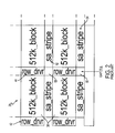
Now referring to the figures, where like reference numbers designate like elements, FIG. 4 shows a 128 megabit portion of a DDR SDRAM integrated circuit 110 constructed in accordance with an exemplary embodiment of the invention. The SDRAM 110 includes a throat region 160 centrally located between two 64 megabit arrays 120 a, 120 b. The first array 120 a contains at least one memory block 130 a and sense amplifier circuit 152 a. Digit lines 180 a of the first array 120 a are organized in a vertical direction while row lines 182 of the first and second arrays 120 a, 120 b are organized in a horizontal direction. The second array 120 b contains at least one memory block 130 b and sense amplifier circuit 152 b. Digit lines 180 b of the second array 120 b are organized in a vertical direction. It should be noted that the invention is not limited to the illustrated size of the first and second arrays 120 a, 120 b. That is, the invention could use first and second arrays 120 a, 120 b greater than or less than 64 megabits depending upon the desired application. Likewise, although the invention provides a DDR SDRAM having a size of at least one gigabit, the invention is not to be limited to any particular size.
In the illustrated embodiment, the throat 160 contains only a datapath 170. Unlike the SDRAM 10 of FIG. 3, two unidirectional row logic circuits 164 a, 164 b are used in the illustrated SDRAM 110. The term “unidirectional” is used to represent the fact that the row logic circuits 164 a, 164 b respectively drive one array 120 a, 120 b in one direction relative to the circuits 164 a, 164 b. That is, a first unidirectional row logic circuit 164 a is connected to and associated with the first array 130 a only and a second unidirectional row logic circuit 164 b is connected to and associated with the second array 130 b only. “Unidirectional” does not mean that the conductors between the row logic circuits 164 a, 164 b and their respective array 120 a, 120 b are special conductors only allowing signals to be transmitted in one direction. That is, any conductors can be used between the row logic circuits 164 a, 164 b and their respective array 120 a, 120 b even though the row logic circuits 164 a, 164 b are considered unidirectional.
The first row logic circuit 164 a contains LT drivers 162 a and array drivers 166 a . The LT drivers 162 a are global row decoders that drive LT lines 168 a connected to the row drivers of the first array 120 a in a unidirectional manner. The array drivers 166 a include PH (phase), EQ (equilibration), ISO (isolation), NSA (n-sense amplifier control), PSA (p-sense amplifier control) drivers required to drive lines 167 a connected to the sense amplifier circuitry 152 a of the first array 120 a. Thus, the first row logic circuit 164 a is not located within the throat 160 and supports only the first array 120 a (i.e., unidirectional). The significance of this architecture is explained below.
The second row logic circuit 164 b contains LT drivers 162 b and array drivers 166 b. The LT drivers 162 b are global row decoders that drive LT lines 168 b connected to the row drivers of the second array 120 b in a unidirectional manner. The array drivers 166 b include PH (phase), EQ (equilibration), ISO (isolation), NSA (n-sense amplifier control), PSA (p-sense amplifier control) drivers required to drive lines 167 b connected to the sense amplifier circuitry 152 b of the second array 120 b. Thus, the second row logic circuit 164 b is not located within the throat 160 and supports only the second array 120 b (i.e., unidirectional manner).
To understand the significance of using two unidirectional row logic circuits 164 a, 164 b removed from the throat region 160, a brief description of how the layers of the SDRAM 110 are organized is now provided. Referring to FIG. 5A, which shows a portion of the IC memory device in perspective view, and to FIG. 5B, which shows the same portion in an elevated sectional view, the integrated circuit 110 includes a substrate assembly 200 and a conductor portion 210. The conductor portion 210 defines at least first 220, second 230, and third 240 layers of metalization. It should be noted that a layer of metalization includes a plurality of discrete traces 242 or conductors arranged in a pattern. Accordingly a first set of traces defines a metal-1 220 layer, a second set of traces defines a metal-2 230 layer, and a third set of traces defines a metal-3 240 layer.
The invention uses three layers of metal traces 242 deposited on layers of insulation 280 disposed above a substrate assembly 200. In a particular embodiment, the present invention includes three layers of metal traces 220, 230, 240 disposed above, and substantially parallel to an upper surface 205 of a substrate assembly 200. The substrate assembly includes doped active regions, gate stacks, polysilicon plugs and a limited number of polysilicon lines. In addition, as known in the art capacitor structures are also fabricated in the memory array above the surface 205 of the substrate and below the three layers of metalization.
Each metal layer is disposed in spaced relation to the other metal layers, and to the substrate assembly 200 of the integrated circuit 110, which contains fabricated devices. Interlayer insulating regions are defined between adjacent layers of metal, and between the metal-1 layer 220 and the substrate assembly 200 of the integrated circuit 110. Thus, a first interlayer region 250 is provided between metal-1 and a surface 205 of the substrate assembly 200 of the integrated circuit 100, a second interlayer region 260 is provided between metal-2 and metal-1, and a third interlayer region 270 is provided between metal-3 and metal-2. Electrically insulating material 280 is generally placed throughout the interlayer regions. As is understood in the art, one or more conventional materials may be used for this purpose.
Since each row logic circuit 164 a, 164 b supports one 64 megabit array 120 a, 120 b instead of two, they are designed to be unidirectional. As such, metal-2 and metal-3 layers are interleaved in parallel throughout the length of the row logic circuits 164 a, 164 b, utilizing maximum routing and power bussing efficiency; thus, increasing performance of the SDRAM 110. This allows a redesign of the LT driver 162 a, 162 b using buried digit lines. The change in row logic design methodology greatly reduces the design area as compared to the prior art, and subsequently saves die area as the pattern is repeated across the length of the die.
The illustrated datapath 170 contains IO circuits 172 having enough drivers to drive eight bidirectional IO pairs 174 connected to the first and second arrays 120 a, 120 b. The illustrated SDRAM 110 uses eight IO pairs 174 per block 130 a, 130 b to obtain a 4n pre-fetch. Thus, the illustrated embodiment includes four IO pairs in addition to the four IO pairs used in the DDR SDRAM 10 illustrated in FIG. 3. Thus, the illustrated DDR SDRAM contains two times the number of IO pairs per block than prior SDRAMs. In a desired embodiment, the additional four IO pairs are routed across the array cores, running parallel to the LT metal-2 lines (thus being shielded by them) as shown in FIG. 5B. The additional IO pairs are routed to metal-3 over the array gap cells 50 and are dropped into the sense amplifier circuits 152 a, 152 b at the array gap cells 50 as shown by arrow A (illustrated in FIG. 5C). Thus, in the desired embodiment, the sense amplifier cell height is unaffected by the additional IO signal lines. As such, the illustrated SDRAM 110 utilizes standard sense amplifier circuitry. This means that the SDRAM 110 has twice as many IO pairs, yet does not have increased die size in comparison to prior SDRAMs (e.g., SDRAM 10 of FIG. 3).
In a desired embodiment, the arrays 120 a, 120 b share the same power bussing. That is, the arrays 120 a, 120 b share a power supply bus such as an array Vcc bus and an array ground potential bus (Gnd bus). The datapath 170, on the other hand, is connected to periphery Vcc and Gnd power bussing. The separation of the array and periphery power bussing prevents power spikes and other sensitivities that may be experienced in the SDRAM 10 illustrated in FIG. 3. Moreover, the separation of the row logic and datapath from a centralized throat region also simplifies the interface and hookup from peripheral areas (i.e., non-array areas) of the SDRAM 110. This alleviates the congestion of signals and power bussing usually found at these areas. This also improves the overall performance of the SDRAM 110 in comparison to the SDRAM 10 (FIG. 3).
FIG. 6 illustrates an exemplary processing system 900 which may utilize a memory device 110 constructed in accordance with an embodiment of the present invention. That is, the memory device 110 is a DDR SDRAM having unidirectional row logic, increased IO lines, and improved routing and power bussing as illustrated in FIG. 4.
The processing system 900 includes one or more processors 901 coupled to a local bus 904. A memory controller 902 and a primary bus bridge 903 are also coupled to the local bus 904. The processing system 900 may include multiple memory controllers 902 and/or multiple primary bus bridges 903. The memory controller 902 and the primary bus bridge 903 may be integrated as a single device 906.
The memory controller 902 is also coupled to one or more memory buses 907. Each memory bus accepts memory components 908 which include at least one memory device 110 of the present invention. The memory components 908 may be a memory card or a memory module. Examples of memory modules include single inline memory modules (SIMMs) and dual inline memory modules (DIMMs). The memory components 908 may include one or more additional devices 909. For example, in a SIMM or DIMM, the additional device 909 might be a configuration memory, such as a serial presence detect (SPD) memory. The memory controller 902 may also be coupled to a cache memory 905. The cache memory 905 may be the only cache memory in the processing system. Alternatively, other devices, for example, processors 901 may also include cache memories, which may form a cache hierarchy with cache memory 905. If the processing system 900 include peripherals or controllers which are bus masters or which support direct memory access (DMA), the memory controller 902 may implement a cache coherency protocol. If the memory controller 902 is coupled to a plurality of memory buses 907, each memory bus 907 may be operated in parallel, or different address ranges may be mapped to different memory buses 907.
The primary bus bridge 903 is coupled to at least one peripheral bus 910. Various devices, such as peripherals or additional bus bridges may be coupled to the peripheral bus 910. These devices may include a storage controller 911, a miscellaneous I/O device 914, a secondary bus bridge 915, a multimedia processor 918, and a legacy device interface 920. The primary bus bridge 903 may also be coupled to one or more special purpose high speed ports 922. In a personal computer, for example, the special purpose port might be the Accelerated Graphics Port (AGP), used to couple a high performance video card to the processing system 900.
The storage controller 911 couples one or more storage devices 913, via a storage bus 912, to the peripheral bus 910. For example, the storage controller 911 may be a SCSI controller and storage devices 913 may be SCSI discs. The I/O device 914 may be any sort of peripheral. For example, the I/O device 914 may be a local area network interface, such as an Ethernet card. The secondary bus bridge 915 may be used to interface additional devices via another bus 916 to the processing system. For example, the secondary bus bridge 915 may be a universal serial port (USB) controller used to couple USB devices 917 to the processing system 900. The multimedia processor 918 may be a sound card, a video capture card, or any other type of media interface, which may also be coupled to additional devices such as speakers 919. The legacy device interface 920 is used to couple legacy devices 921, for example, older styled keyboards and mice, to the processing system 900.
The processing system 900 illustrated in FIG. 6 is only an exemplary processing system with which the invention may be used. While FIG. 6 illustrates a processing architecture especially suitable for a general purpose computer, such as a personal computer or a workstation, it should be recognized that well known modifications can be made to configure the processing system 900 to become more suitable for use in a variety of applications. For example, many electronic devices which require processing may be implemented using a simpler architecture which relies on a CPU 901 coupled to memory components 908 and/or memory devices 110. These electronic devices may include, but are not limited to audio/video processors and recorders, gaming consoles, digital television sets, wired or wireless telephones, navigation devices (including system based on the global positioning system (GPS) and/or inertial navigation), and digital cameras and/or recorders. The modifications may include, for example, elimination of unnecessary components, addition of specialized devices or circuits, and/or integration of a plurality of devices.
The processes and devices described above illustrate exemplary methods and typical devices of many that could be used and produced. The above description and drawings illustrate embodiments, which achieve the objects, features, and advantages of the present invention. However, it is not intended that the present invention be strictly limited to the above-described and illustrated embodiments. Any modification, though presently unforeseeable, of the present invention that comes within the spirit and scope of the following claims should be considered part of the present invention.

Claims (24)

What is claimed as new and desired to be protected by Letters Patent of the United States is:
1. A memory device comprising:
a substrate;
a first metal layer provided over the substrate;
a second metal layer provided over the first metal layer;
a third metal layer provided over the second metal layer, wherein the first metal layer, the second metal layer and the third metal layer are disposed in a substantially parallel spaced relation;
first and second arrays of memory cells separated by and in communication with a throat region, said first and second arrays of memory cells being the only memory cells adjacent to and in communication with said throat region, said first and second arrays comprising a plurality of memory blocks, said throat region being positioned between the first and second arrays and consisting essentially of a datapath, said datapath comprising a plurality of IO circuits with each IO circuit being connected to and associated with a respective memory block from said first and second arrays, wherein a first portion of said plurality of IO circuits is routed through the second metal layer and a second different portion of said plurality of IO circuits is routed through the third metal layer, wherein no IO circuits are routed through the first metal layer;
a first row logic circuit respectively connected to and associated with said first array and being on a first side of said first array opposite a second side of said first array, the second side of the first array adjoining said throat region, wherein said first row logic circuit provides signals to said first array in a unidirectional manner, the first array comprising a separate, independently addressable circuit comprising a set of row lines and a set of digit lines; and
a second row logic circuit respectively connected to and associated with said second array and being on a first side of said second array opposite a second side of said second array, the second side of the second array adjoining said throat region,
wherein said arrays are connected to a first power bus and a first ground bus, and said throat region is connected to a second power bus and a second ground bus, which are separate than the first power and ground busses,
wherein said IO circuits are associated with respective IO lines, and wherein at least some of said IO lines are routed across the first and second arrays, the at least some of said IO lines running parallel to row-driver lines in the second metal layer and being routed to the third metal layer through the second metal layer over gap cells in the first and second arrays.
2. The device of claim 1, wherein said first row logic circuit comprises a global driver for driving signal lines connected to said first array.
3. The device of claim 1, wherein said first row logic circuit comprises array drivers for driving signal lines connected to sense amplifier circuitry within said first array.
4. The device of claim 1, wherein said second row logic circuit provides signals to said second array in a unidirectional manner.
5. The device of claim 4, wherein said second row logic circuit comprises a global driver for driving signal lines connected to said second array.
6. The device of claim 4, wherein said second row logic circuit comprises array drivers for driving signal lines connected to sense amplifier circuitry within said second array.
7. The device of claim 1, wherein said datapath is connected to the IO lines.
8. The device of claim 1, wherein said first row logic circuit is disposed at a periphery of said first array at a side opposite said throat region.
9. The device of claim 1, wherein said second row logic circuit is disposed at a periphery of said second array at a side opposite said throat region.
10. The device of claim 1, wherein said device is a double data rate synchronous dynamic random access memory device.
11. The device of claim 1, wherein said first and second arrays comprise a plurality of 512 kilobit memory blocks.
12. The device of claim 1, wherein said first and second arrays each comprise 128 megabits.
13. A processor system comprising:
a processor; and
a memory device coupled to said processor, said memory device comprising:
a substrate;
a first metal layer provided over the substrate;
a second metal layer provided over the first metal layer;
a third metal layer provided over the second metal layer, wherein the first metal layer, the second metal layer and the third metal layer are disposed in a substantially parallel spaced relation;
first and second arrays of memory cells separated by and in communication with a throat region, said first and second arrays of memory cells being the only memory cells adjacent to said throat region and in communication with, said first and second arrays comprising a plurality of memory blocks, said throat region being positioned between the first and second arrays and consisting essentially of a datapath, said datapath comprising a plurality of IO circuits with each IO circuit being connected to and associated with a respective memory block from said first and second arrays wherein a first portion of said plurality of IO circuits is routed through the second metal layer and a second different portion of said plurality of IO circuits is routed through the third metal layer, wherein no IO circuits are routed through the first metal layer;
a first row logic circuit respectively connected to and associated with said first array and on a first side of said first array opposite a second side of said first array, the second side of the first array adjoining said throat region, wherein said first row logic circuit provides signals to said first array in a unidirectional manner, the first array comprising a separate, independently addressable circuit comprising a set of row lines and a set of digit lines; and
a second row logic circuit respectively connected to and associated with said second array and being on a first side of said second array opposite a second side of said second array, the second side of the second array adjoining said throat region,
wherein said arrays are connected to a first power bus and a first ground bus, and said throat region is connected to a second power bus, which are separate than the first power and ground busses,
wherein said IO circuits are associated with respective IO lines, and wherein at least some of said IO lines are routed across the first and second arrays, the at least some of said IO lines running parallel to row-driver lines in the second metal layer and being routed to the third metal layer through the second metal layer over gap cells in the first and second arrays.
14. The system of claim 13, wherein said first row logic circuit comprises a global driver for driving signal lines connected to said first array.
15. The system of claim 13, wherein said first row logic circuit comprises array drivers for driving signal lines connected to sense amplifier circuitry within said first array.
16. The system of claim 13, wherein said second row logic circuit provides signals to said second array in a unidirectional manner.
17. The system of claim 16, wherein said second row logic circuit comprises a global driver for driving signal lines connected to said second array.
18. The system of claim 16, wherein said second row logic circuit comprises array drivers for driving signal lines connected to sense amplifier circuitry within said second array.
19. The system of claim 13, wherein said datapath is connected to the IO lines.
20. The system of claim 13, wherein said first row logic circuit is disposed at a periphery of said first array at a side opposite said throat region.
21. The system of claim 13, wherein said second row logic circuit is disposed at a periphery of said second array at a side opposite said throat region.
22. The system of claim 13, wherein said memory device is a double data rate synchronous dynamic random access memory device.
23. The system of claim 13, wherein said first and second arrays comprise a plurality of 512 kilobit memory blocks.
24. The system of claim 13, wherein said first and second arrays each comprise 128 megabits.
US11/476,744 2004-06-30 2006-06-29 Memory architecture Expired - Fee Related US8897052B2 (en)

Priority Applications (1)

Application Number Priority Date Filing Date Title
US11/476,744 US8897052B2 (en) 2004-06-30 2006-06-29 Memory architecture

Applications Claiming Priority (2)

Application Number Priority Date Filing Date Title
US10/879,158 US7236385B2 (en) 2004-06-30 2004-06-30 Memory architecture
US11/476,744 US8897052B2 (en) 2004-06-30 2006-06-29 Memory architecture

Related Parent Applications (1)

Application Number Title Priority Date Filing Date
US10/879,158 Continuation US7236385B2 (en) 2004-06-30 2004-06-30 Memory architecture

Publications (2)

Publication Number Publication Date
US20060245231A1 US20060245231A1 (en) 2006-11-02
US8897052B2 true US8897052B2 (en) 2014-11-25

Family

ID=35599241

Family Applications (2)

Application Number Title Priority Date Filing Date
US10/879,158 Expired - Fee Related US7236385B2 (en) 2004-06-30 2004-06-30 Memory architecture
US11/476,744 Expired - Fee Related US8897052B2 (en) 2004-06-30 2006-06-29 Memory architecture

Family Applications Before (1)

Application Number Title Priority Date Filing Date
US10/879,158 Expired - Fee Related US7236385B2 (en) 2004-06-30 2004-06-30 Memory architecture

Country Status (1)

Country Link
US (2) US7236385B2 (en)

Families Citing this family (6)

* Cited by examiner, † Cited by third party
Publication number Priority date Publication date Assignee Title
US7236385B2 (en) * 2004-06-30 2007-06-26 Micron Technology, Inc. Memory architecture
US7936639B2 (en) * 2007-09-27 2011-05-03 Micron Technology, Inc. System and method for processing signals in high speed DRAM
US7944773B2 (en) * 2008-04-30 2011-05-17 Micron Technology, Inc. Synchronous command-based write recovery time auto-precharge control
US9190144B2 (en) * 2012-10-12 2015-11-17 Micron Technology, Inc. Memory device architecture
US9368443B1 (en) * 2015-01-20 2016-06-14 Taiwan Semiconductor Manufacturing Company, Ltd. Memory metal scheme
CN108780791B (en) * 2016-03-01 2023-01-10 索尼公司 Semiconductor device, electronic module, electronic apparatus, and method for producing semiconductor device

Citations (25)

* Cited by examiner, † Cited by third party
Publication number Priority date Publication date Assignee Title
US4295149A (en) 1978-12-29 1981-10-13 International Business Machines Corporation Master image chip organization technique or method
US5412613A (en) * 1993-12-06 1995-05-02 International Business Machines Corporation Memory device having asymmetrical CAS to data input/output mapping and applications thereof
US5459093A (en) 1993-03-18 1995-10-17 Sony Corporation Method for forming dummy pattern in a semiconductor device
US5751031A (en) * 1995-05-01 1998-05-12 Micron Technology, Inc. Memory and other integrated circuitry having a conductive interconnect line pitch of less than 0.6 micron
US5838627A (en) * 1994-05-20 1998-11-17 Mitsubishi Denki Kabushiki Kaisha Arrangement of power supply and data input/output pads in semiconductor memory device
US5914910A (en) * 1994-09-27 1999-06-22 Matsushita Electric Industrial Co., Ltd. Semiconductor memory and method of using the same column decoder and image processor
US5973976A (en) * 1997-10-23 1999-10-26 Mitsubishi Denki Kabushiki Kaisha Logic semiconductor integrated circuit device having embedded dynamic random-access memory
US6072744A (en) * 1998-07-21 2000-06-06 Hyundai Electronics Industries Co., Ltd. Memory device having data bus lines of uniform length
US6166942A (en) * 1998-08-21 2000-12-26 Micron Technology, Inc. Embedded DRAM architecture with local data drivers and programmable number of data read and data write lines
US6184122B1 (en) 1998-12-17 2001-02-06 United Microelectronics Corp. Method for preventing crosstalk between conductive layers
US20010026483A1 (en) * 2000-03-29 2001-10-04 Masatoshi Hasegawa Semiconductor memory device
US6314011B1 (en) 1997-08-22 2001-11-06 Micron Technology Inc 256 Meg dynamic random access memory
US6345011B2 (en) * 2000-01-10 2002-02-05 Samsung Electronics Co., Ltd. Input/output line structure of a semiconductor memory device
US6355982B2 (en) 1997-12-18 2002-03-12 Kabushiki Kaisha Toshiba Semiconductor memory device having pairs of bit lines arranged on both sides of memory cells
US6396766B1 (en) * 2000-10-25 2002-05-28 Samsung Electronics Co., Ltd. Semiconductor memory architecture for minimizing input/output data paths
US6445065B1 (en) * 2000-06-06 2002-09-03 In-Chip Systems, Inc. Routing driven, metal programmable integrated circuit architecture with multiple types of core cells
US20020131289A1 (en) * 2001-03-15 2002-09-19 J. Wayne Thompson Metal during pattern for memory devices
US6515937B2 (en) * 1995-10-04 2003-02-04 Kabushiki Kaisha Toshiba Test circuit for testing semiconductor memory
US6556065B1 (en) * 1997-05-30 2003-04-29 Micron Technology, Inc. 256 Meg dynamic random access memory
US20030110348A1 (en) * 2001-12-07 2003-06-12 Janzen Jeffery W. Sequential nibble burst ordering for data
US20040037141A1 (en) * 2002-08-23 2004-02-26 Micron Technology, Inc. DRAM power bus control
US6754802B1 (en) 2000-08-25 2004-06-22 Micron Technology, Inc. Single instruction multiple data massively parallel processor systems on a chip and system using same
US7138716B2 (en) * 2003-06-27 2006-11-21 Intel Corporation Addition of metal layers with signal reallocation to a microprocessor for increased frequency and lower power
US7230340B2 (en) * 2000-10-18 2007-06-12 Megica Corporation Post passivation interconnection schemes on top of the IC chips
US7236385B2 (en) * 2004-06-30 2007-06-26 Micron Technology, Inc. Memory architecture

Family Cites Families (2)

* Cited by examiner, † Cited by third party
Publication number Priority date Publication date Assignee Title
US6091090A (en) * 1997-09-19 2000-07-18 In-Chip Systems, Inc. Power and signal routing technique for gate array design
JP3862220B2 (en) * 2002-07-29 2006-12-27 松下電器産業株式会社 Semiconductor memory device

Patent Citations (27)

* Cited by examiner, † Cited by third party
Publication number Priority date Publication date Assignee Title
US4295149A (en) 1978-12-29 1981-10-13 International Business Machines Corporation Master image chip organization technique or method
US5459093A (en) 1993-03-18 1995-10-17 Sony Corporation Method for forming dummy pattern in a semiconductor device
US5412613A (en) * 1993-12-06 1995-05-02 International Business Machines Corporation Memory device having asymmetrical CAS to data input/output mapping and applications thereof
US5838627A (en) * 1994-05-20 1998-11-17 Mitsubishi Denki Kabushiki Kaisha Arrangement of power supply and data input/output pads in semiconductor memory device
US5914910A (en) * 1994-09-27 1999-06-22 Matsushita Electric Industrial Co., Ltd. Semiconductor memory and method of using the same column decoder and image processor
US5751031A (en) * 1995-05-01 1998-05-12 Micron Technology, Inc. Memory and other integrated circuitry having a conductive interconnect line pitch of less than 0.6 micron
US6515937B2 (en) * 1995-10-04 2003-02-04 Kabushiki Kaisha Toshiba Test circuit for testing semiconductor memory
US6556065B1 (en) * 1997-05-30 2003-04-29 Micron Technology, Inc. 256 Meg dynamic random access memory
US6314011B1 (en) 1997-08-22 2001-11-06 Micron Technology Inc 256 Meg dynamic random access memory
US5973976A (en) * 1997-10-23 1999-10-26 Mitsubishi Denki Kabushiki Kaisha Logic semiconductor integrated circuit device having embedded dynamic random-access memory
US6355982B2 (en) 1997-12-18 2002-03-12 Kabushiki Kaisha Toshiba Semiconductor memory device having pairs of bit lines arranged on both sides of memory cells
US6072744A (en) * 1998-07-21 2000-06-06 Hyundai Electronics Industries Co., Ltd. Memory device having data bus lines of uniform length
US6166942A (en) * 1998-08-21 2000-12-26 Micron Technology, Inc. Embedded DRAM architecture with local data drivers and programmable number of data read and data write lines
US6184122B1 (en) 1998-12-17 2001-02-06 United Microelectronics Corp. Method for preventing crosstalk between conductive layers
US6345011B2 (en) * 2000-01-10 2002-02-05 Samsung Electronics Co., Ltd. Input/output line structure of a semiconductor memory device
US20010026483A1 (en) * 2000-03-29 2001-10-04 Masatoshi Hasegawa Semiconductor memory device
US6445065B1 (en) * 2000-06-06 2002-09-03 In-Chip Systems, Inc. Routing driven, metal programmable integrated circuit architecture with multiple types of core cells
US6754802B1 (en) 2000-08-25 2004-06-22 Micron Technology, Inc. Single instruction multiple data massively parallel processor systems on a chip and system using same
US7230340B2 (en) * 2000-10-18 2007-06-12 Megica Corporation Post passivation interconnection schemes on top of the IC chips
US6396766B1 (en) * 2000-10-25 2002-05-28 Samsung Electronics Co., Ltd. Semiconductor memory architecture for minimizing input/output data paths
US20020131289A1 (en) * 2001-03-15 2002-09-19 J. Wayne Thompson Metal during pattern for memory devices
US6664634B2 (en) * 2001-03-15 2003-12-16 Micron Technology, Inc. Metal wiring pattern for memory devices
US20030110348A1 (en) * 2001-12-07 2003-06-12 Janzen Jeffery W. Sequential nibble burst ordering for data
US20040037141A1 (en) * 2002-08-23 2004-02-26 Micron Technology, Inc. DRAM power bus control
US6795365B2 (en) * 2002-08-23 2004-09-21 Micron Technology, Inc. DRAM power bus control
US7138716B2 (en) * 2003-06-27 2006-11-21 Intel Corporation Addition of metal layers with signal reallocation to a microprocessor for increased frequency and lower power
US7236385B2 (en) * 2004-06-30 2007-06-26 Micron Technology, Inc. Memory architecture

Non-Patent Citations (1)

* Cited by examiner, † Cited by third party
Title
Merriam-Webster Online Dictionary Printout (www.merriam-webster.com/dictionary/adjacent). *

Also Published As

Publication number Publication date
US20060013056A1 (en) 2006-01-19
US20060245231A1 (en) 2006-11-02
US7236385B2 (en) 2007-06-26

Similar Documents

Publication Publication Date Title
US8154004B2 (en) Hybrid MRAM array structure and operation
US6807120B2 (en) Dynamic random access memory (DRAM) capable of canceling out complementary noise developed in plate electrodes of memory cell capacitors
US6940748B2 (en) Stacked 1T-nMTJ MRAM structure
CN111033616B (en) Power supply wiring in semiconductor memory device
WO2014185669A1 (en) Stack memory
US8897052B2 (en) Memory architecture
US5636158A (en) Irregular pitch layout for a semiconductor memory device
JPH11163299A (en) Semiconductor memory
JP2006013337A (en) Three-dimensional semiconductor device
US6765814B2 (en) Semiconductor memory device
JP2785655B2 (en) Semiconductor device
US6947308B2 (en) Embedded semiconductor memory with crossbar wirings and switches for high bandwidth
JP3345282B2 (en) Design method of semiconductor integrated circuit device
CN102810557A (en) Method for manufacturing semiconductor device
JPH11330414A (en) Semiconductor memory device
US6317358B1 (en) Efficient dual port DRAM cell using SOI technology
JP4474424B2 (en) Semiconductor integrated circuit device
EP0913831B1 (en) Space-efficient master data line (MDQ) switch placement
JPS6386186A (en) Semiconductor storage device
KR20010002116A (en) Semiconductor integrated circuit using SRAM between DRAM and logic circuit as buffer
JPH11135748A (en) Semiconductor integrated circuit device
JP2002008377A (en) Semiconductor device
JPH0828475B2 (en) Multi-bit configuration semiconductor memory

Legal Events

Date Code Title Description
AS Assignment

Owner name: ROUND ROCK RESEARCH, LLC,NEW YORK

Free format text: ASSIGNMENT OF ASSIGNORS INTEREST;ASSIGNOR:MICRON TECHNOLOGY, INC.;REEL/FRAME:023786/0416

Effective date: 20091223

Owner name: ROUND ROCK RESEARCH, LLC, NEW YORK

Free format text: ASSIGNMENT OF ASSIGNORS INTEREST;ASSIGNOR:MICRON TECHNOLOGY, INC.;REEL/FRAME:023786/0416

Effective date: 20091223

FEPP Fee payment procedure

Free format text: MAINTENANCE FEE REMINDER MAILED (ORIGINAL EVENT CODE: REM.)

LAPS Lapse for failure to pay maintenance fees

Free format text: PATENT EXPIRED FOR FAILURE TO PAY MAINTENANCE FEES (ORIGINAL EVENT CODE: EXP.); ENTITY STATUS OF PATENT OWNER: LARGE ENTITY

STCH Information on status: patent discontinuation

Free format text: PATENT EXPIRED DUE TO NONPAYMENT OF MAINTENANCE FEES UNDER 37 CFR 1.362

FP Lapsed due to failure to pay maintenance fee

Effective date: 20181125