US8901747B2 - Semiconductor chip layout - Google Patents
Semiconductor chip layout Download PDFInfo
- Publication number
- US8901747B2 US8901747B2 US12/846,763 US84676310A US8901747B2 US 8901747 B2 US8901747 B2 US 8901747B2 US 84676310 A US84676310 A US 84676310A US 8901747 B2 US8901747 B2 US 8901747B2
- Authority
- US
- United States
- Prior art keywords
- die
- data lines
- semiconductor device
- package substrate
- cores
- Prior art date
- Legal status (The legal status is an assumption and is not a legal conclusion. Google has not performed a legal analysis and makes no representation as to the accuracy of the status listed.)
- Active, expires
Links
Images


Classifications
-
- H—ELECTRICITY
- H01—ELECTRIC ELEMENTS
- H01L—SEMICONDUCTOR DEVICES NOT COVERED BY CLASS H10
- H01L23/00—Details of semiconductor or other solid state devices
- H01L23/48—Arrangements for conducting electric current to or from the solid state body in operation, e.g. leads, terminal arrangements ; Selection of materials therefor
- H01L23/50—Arrangements for conducting electric current to or from the solid state body in operation, e.g. leads, terminal arrangements ; Selection of materials therefor for integrated circuit devices, e.g. power bus, number of leads
-
- H—ELECTRICITY
- H01—ELECTRIC ELEMENTS
- H01L—SEMICONDUCTOR DEVICES NOT COVERED BY CLASS H10
- H01L2224/00—Indexing scheme for arrangements for connecting or disconnecting semiconductor or solid-state bodies and methods related thereto as covered by H01L24/00
- H01L2224/01—Means for bonding being attached to, or being formed on, the surface to be connected, e.g. chip-to-package, die-attach, "first-level" interconnects; Manufacturing methods related thereto
- H01L2224/10—Bump connectors; Manufacturing methods related thereto
- H01L2224/15—Structure, shape, material or disposition of the bump connectors after the connecting process
- H01L2224/16—Structure, shape, material or disposition of the bump connectors after the connecting process of an individual bump connector
- H01L2224/161—Disposition
- H01L2224/16151—Disposition the bump connector connecting between a semiconductor or solid-state body and an item not being a semiconductor or solid-state body, e.g. chip-to-substrate, chip-to-passive
- H01L2224/16221—Disposition the bump connector connecting between a semiconductor or solid-state body and an item not being a semiconductor or solid-state body, e.g. chip-to-substrate, chip-to-passive the body and the item being stacked
- H01L2224/16225—Disposition the bump connector connecting between a semiconductor or solid-state body and an item not being a semiconductor or solid-state body, e.g. chip-to-substrate, chip-to-passive the body and the item being stacked the item being non-metallic, e.g. insulating substrate with or without metallisation
- H01L2224/16235—Disposition the bump connector connecting between a semiconductor or solid-state body and an item not being a semiconductor or solid-state body, e.g. chip-to-substrate, chip-to-passive the body and the item being stacked the item being non-metallic, e.g. insulating substrate with or without metallisation the bump connector connecting to a via metallisation of the item
-
- H—ELECTRICITY
- H01—ELECTRIC ELEMENTS
- H01L—SEMICONDUCTOR DEVICES NOT COVERED BY CLASS H10
- H01L2924/00—Indexing scheme for arrangements or methods for connecting or disconnecting semiconductor or solid-state bodies as covered by H01L24/00
-
- H—ELECTRICITY
- H01—ELECTRIC ELEMENTS
- H01L—SEMICONDUCTOR DEVICES NOT COVERED BY CLASS H10
- H01L2924/00—Indexing scheme for arrangements or methods for connecting or disconnecting semiconductor or solid-state bodies as covered by H01L24/00
- H01L2924/0001—Technical content checked by a classifier
- H01L2924/0002—Not covered by any one of groups H01L24/00, H01L24/00 and H01L2224/00
-
- H—ELECTRICITY
- H01—ELECTRIC ELEMENTS
- H01L—SEMICONDUCTOR DEVICES NOT COVERED BY CLASS H10
- H01L2924/00—Indexing scheme for arrangements or methods for connecting or disconnecting semiconductor or solid-state bodies as covered by H01L24/00
- H01L2924/15—Details of package parts other than the semiconductor or other solid state devices to be connected
- H01L2924/151—Die mounting substrate
- H01L2924/1517—Multilayer substrate
- H01L2924/15192—Resurf arrangement of the internal vias
-
- H—ELECTRICITY
- H01—ELECTRIC ELEMENTS
- H01L—SEMICONDUCTOR DEVICES NOT COVERED BY CLASS H10
- H01L2924/00—Indexing scheme for arrangements or methods for connecting or disconnecting semiconductor or solid-state bodies as covered by H01L24/00
- H01L2924/15—Details of package parts other than the semiconductor or other solid state devices to be connected
- H01L2924/151—Die mounting substrate
- H01L2924/153—Connection portion
- H01L2924/1531—Connection portion the connection portion being formed only on the surface of the substrate opposite to the die mounting surface
- H01L2924/15311—Connection portion the connection portion being formed only on the surface of the substrate opposite to the die mounting surface being a ball array, e.g. BGA
Definitions
- Latency is the time lapsed between an event in an input signal and a corresponding event in an output signal that results from the event in the input signal. For example, in a memory circuit latency is the time lapsed between the receipt of a ‘Read’ command at an input pin of the memory circuit and the transmission of the corresponding read data to the output pins of the memory circuit.
- serializer-deserializer (SERDES) circuits convert data packets between serial and parallel formats. It is common practice to place the SERDES circuits and other associated logic components along the periphery of the silicon chip. Such architecture results in a wide spread in latencies in the silicon, depending on the distance between the SERDES and the specific functional block that is the source or the destination of the data. Thus, worst case timing latency is determined by the longest path set by the I/O which is the furthest away from any one device resource. A typical layout of I/O at the periphery would result in the worst case path from one corner of the die to the opposite corner. The resulting distance that an input signal must traverse could be the width plus the height of the die.
- Error rates are expected to increase for high speed data links.
- Many circuits have a cyclic redundancy check (CRC) circuit to perform error checking on data packets. Error checking is performed across the entire data packet, which may be striped across multiple data lines to increase bandwidth and to reduce latency.
- CRC cyclic redundancy check
- Error checking is performed across the entire data packet, which may be striped across multiple data lines to increase bandwidth and to reduce latency.
- CRC cyclic redundancy check
- heaviest packet traffic in a device typically occurs as communication among functional blocks formed in or on the silicon substrate.
- Data lines formed in or on the silicon substrate are dimensionally constrained, thus representing significant capacitive and resistive loads to the paths the signals must traverse.
- communication lines in or on silicon further need to circumvent the functional blocks that create barriers to signal routing, adding to the lengths of the communication lines.
- on die packet traffic routed through communication lines on a silicon substrate with a significant density of functional blocks will experience increased latencies.
- Tx/Rx differential pairs are typically grouped closely together in high speed communication systems.
- Each Tx transmitter includes a transmit channel that conveys read data and status information out of a package.
- Each Rx receiver includes a receive channel that receives address, control and write data from outside of the package.
- the proximity of Tx and Rx channels can result in data crosstalk and an increase in bit flips.
- Hall separates transmitter contacts from receiver contacts in a high speed interface pattern.
- Tx data channels in Hall's pattern must be positioned parallel to Rx data channels to convey data from the transmitter out to the host.
- Parallel Tx/Rx channels tend to degrade data signals and increase error rates.
- the data line transporting a high speed Tx signal must cross over an Rx data line before exiting the PC board.
- Such proximity of Rx contacts to Tx contacts contributes to noise coupling between Tx and Rx signals.
- Hall does not resolve the problem of Inter Signal Interference (ISI) for high speed data links.
- ISI Inter Signal Interference
- the present invention provides a layout for a semiconductor device coupled to a second device.
- IP cores functional circuit blocks
- a serial interface is centered on the die between the two IP cores.
- the serial interface includes multiple ports which serve as nodes coupled to various data lines.
- the serial interface includes multiple transmitter ports and multiple receiver ports. The ports are coupled together by Tx data lines and Rx data lines.
- the die itself has multiple metal layers and is encapsulated in a package having multiple routing layers.
- the present invention is also directed to a semiconductor device coupled to a second device, where the semiconductor device contains a die divided into two partitions.
- An IP core is contained in each partition.
- multiple receiver terminals are located in the first partition of the die, and multiple transmitter terminals are located in the second partition of the die.
- a serial interface is further incorporated on the die and is positioned adjacent to one of the IP cores, wherein the serial interface includes transmitter ports and receiver ports.
- the IC device also includes Tx data lines, originating from respective Tx ports wherein each Tx port serializes and transmits a serial data signal for output on a Tx data line to one of said IP cores; and Rx data lines, originating from respective receiver ports, wherein each receiver port receives and deserializes a serial data signal for output on an Rx data line to one of said IP cores.
- Another embodiment of the invention is directed to a stacked die that includes multiple dies attached together. At least one die in the stack assembly has Rx terminals in a first partition of the die and Tx terminals in a second partition of the die. At least one of the dies in the stack has a serial interface in a central region of the chip layout. Thus, it is not necessary for all the dies in the stack assembly to have the same chip layout as the die of the present invention.
- the invention is also directed to a stacked die assembly that operates with reduced power, and propagation delay.
- the reduced driving distance correlated to the layout of the invention reduces the system latency as well as power.
- FIG. 1 illustrates a device layout that includes a memory block and a SERDES interface
- FIG. 2 illustrates a device layout that includes multiple functional blocks and a SERDES interface
- FIG. 3A illustrates a package layout for the embodiment of FIG. 1 ;
- FIG. 3B illustrates the package layout of FIG. 3A with conductor traces
- FIG. 4A illustrates a conventional routing pattern for two ICs mounted on a printed circuit board
- FIG. 4B illustrates the extensive crossover problem that occurs when two conventional chips are positioned next to each other
- FIG. 5A illustrates a routing pattern for two BE devices mounted on a printed circuit board
- FIG. 5B illustrates an alternative routing pattern for two BE devices mounted on a printed circuit board
- FIG. 6A illustrates a routing pattern of a BE device coupled to a conventional device on a printed circuit board with a minimal amount of crossover
- FIG. 6B illustrates an alternative routing pattern for the two devices of FIG. 6A ;
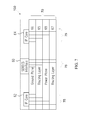
- FIG. 7 illustrates a cross section of a semiconductor package of the present invention.
- FIG. 8 illustrates a cross section of a stacked die assembly in accordance with one embodiment of the invention.
- FIG. 1 illustrates a die layout 11 of the present invention divided by an axis 112 into an upper partition 50 and a lower partition 52 .
- Each partition of the die layout contains an IP core 10 A, 10 B that is either a memory array, programmable logic array or network processor block.
- the memory core 10 A, 10 B may b either an SRAM, DRAM, 1T-SRAM or Flash.
- a serial interface 115 is positioned on axis 112 between the two IP cores 10 A, 10 B.
- axis 112 is centrally located on semiconductor die 400 .
- axis 112 can be shifted so that the SERDES interface is positioned off center on die surface 400 .
- the serial interface contains one or more SERDES blocks.
- the semiconductor die of this invention has multiple metal layers 190 , upon which are that contain various circuit patterns.
- each partition may constitute an equivalent half, that is, each partition may have the same area. However, it is not necessary that the partitions of the present invention have the same area as illustrated in FIG. 1 .
- FIG. 2 illustrates an alternate chip layout where partition 50 has a smaller area than partition 52 .
- more than two IP cores are arranged on die 275 .
- the upper partition 50 of substrate 275 is mounted memory core 10 A, logic core 35 A and network processor 25 A.
- the lower partition 52 of substrate 275 contains memory core 10 B, logic core 35 B, and network processor 25 B.
- the layout of FIG. 2 also includes a memory access controller and/or error detection software 40 .
- Each pair of IP cores is preferably symmetrically located about axis 112 .
- axis 112 is positioned a SERDES interface composed of two SERDES blocks 115 .
- Each SERDES block 115 contains Rx/Tx unit 122 a , 124 a/ 122 b , 124 b , respectively.
- Each Tx port in Tx unit 122 b , 124 b contains a differential pair of transmitters, the transmitter pairs are grouped with the transmitters of the same Tx unit.
- Each Rx port in Rx unit 122 a , 124 a contains a differential pair of receivers that are isolated from the Tx ports in Tx unit 122 b , 124 b .
- each Tx port and each Rx port has clocking functionality to implement PLL circuitry.
- the present invention is also applicable to a SERDES block that has a different number of Tx/Rx ports.
- the Rx ports in Rx unit 122 a , 124 a occupy a portion of the upper partition 50 of the die layout and the Tx ports in Tx unit 122 b , 124 b occupy a lower partition 52 of the die layout.
- FIG. 3A illustrates a more detailed layout of the invention.
- Elements 316 - 1 to 316 - 16 correspond to Rx terminals
- elements 315 - 1 to 315 - 16 correspond to Tx terminals.
- the Tx terminals are separated from the Rx terminals. Terminals refer to nodes on the edge of a package that are coupled to data lines.
- the present invention provides connections to Rx/Tx ports inside a serial interface on the die. The ports are equidistant from the four corners of the die substrate to a central region on the die.
- FIG. 3A shows the layout of package substrate 300 in an integrated circuit memory device according to some embodiments of the present invention.
- Divisions 301 of package substrate 300 may overlap different area portions of die substrate 400 which may include functional components (“blocks”) formed in circuit substrate 400 . For example, the divisions in the shaded portion 320 of FIG. 3A may overlap various functional blocks formed in die substrate 400 .
- Such functional blocks may include logic and memory circuits, as well as memory arrays 10 A and 10 B, coupled to SERDES circuits 115 , and CRC circuit 40 of FIG. 1 , which shows a layout of die substrate 400 . While the embodiment depicted in FIG. 1 includes two memory arrays and two SERDES circuits, some embodiments of the present invention may use a different number of memory arrays and SERDES circuits.
- the divisions 301 in portion 321 ( 322 ) of package substrate 300 overlap first (second) SERDES circuit 115 .
- the divisions 301 in portion 310 of package substrate 300 overlap CRC circuit 40 ( FIG. 1 ), according to the embodiment depicted in FIG. 3A .
- a given division 301 in package substrate 300 may overlap more than one functional component formed in die substrate 400 .
- divisions 344 - 1 a ( 344 - 2 a ) and 344 - 1 b ( 344 - 2 b ) may be coupled to conducting balls providing a signal or power to a sensitive circuit like a PLL (phase-locked loop) circuit in substrate 400 .
- Portion 321 ( 322 ) may include receiver portion 321 a ( 322 a ) overlapping receiver unit 122 a ( 124 a ) in SERDES 115 of FIG. 1 .
- Portion 321 ( 322 ) may also include transmitter portion 321 b ( 322 b ) overlapping transmitter unit 122 b ( 124 b ) in SERDES 115 of FIG. 1 .
- portions 315 - 1 to 315 - 16 and portions 316 - 1 to 316 - 16 may be provided outside and along the edges of shaded portion 320 of package substrate 300 , according to the embodiment shown in FIG. 3A .
- Portions 315 - 1 to 315 - 16 overlap divisions 301 of package substrate 300 that may be coupled to Tx data channels 550 - 1 to 550 - 16 of package substrate 300 (see, FIG. 3B ) through conducting balls 215 , according to some embodiments of the present invention.
- Portions 316 - 1 to 316 - 16 overlap divisions 301 of package substrate 300 coupled to Rx data channels 552 - 1 to 552 - 16 (see, FIG. 3B ) through conducting balls 216 .
- Some of the divisions (e.g. 351 and 352 ) in package substrate 300 may be coupled to a biasing voltage for die (circuit) substrate 400 , associated with a ground voltage provided through divisions 361 and 362 , respectively.
- Portion 375 - 1 ( 375 - 2 ) may be used to provide an extra Tx data channel 551 - 1 ( 551 - 2 ) (see, FIG. 3B ) to integrated circuit 100 .
- portions 376 - 1 ( 376 - 2 ) overlap divisions 301 in package substrate 300 that may provide an extra Rx data channel 553 - 1 ( 553 - 2 ) (see, FIG. 3B ) to integrated circuit 100 .
- FIG. 3B is a layout of package substrate 300 showing the positions of conducting balls 215 - 1 a , 215 - 1 b to 215 - 15 a , 215 - 15 b , 216 - 1 a , 216 - 1 b to 216 - 15 a , 216 - 15 b , coupled to package substrate 300 . Also shown are conducting balls 515 - 1 a , 515 - 1 b , 515 - 2 a , 515 - 2 b , 516 - 1 a , and 516 - 1 b , and 516 - 2 a , 516 - 2 b coupled to package substrate 300 . Also shown in FIG.
- the latency of a memory array for a data line in a package substrate having a length of approximately 8-10 mm may be less than 100 picoseconds, and more preferably, the latency is less than 70 picoseconds (ps) or less within the package substrate.
- the latency for a Tx/Rx data line in the prior art carrying data signals from one edge of a die to the opposite edge of the die within a silicon substrate may have a latency ten times greater than the present invention, or about 2.4 ns.
- a Tx signal will take longer to travel from bump 30 in the serial interface 322 b through the die ( 400 of Fig. 1 ) to the die edge than to travel from serial interface 322 b through the package substrate 300 and out to ball 215 - 10 a, b (which is the edge of the package).
- Conducting balls 216 - 1 a,b to 216 - 16 a,b are coupled to Rx data lines 552 - 1 to 552 - 16 ; conducting balls 516 - 1 a,b are coupled to Rx data line 553 - 1 ; and conducting balls 516 - 2 a , 516 - 2 b are coupled to Rx data line 553 - 2 .
- Conducting balls 215 - 1 a , 215 - 1 b to 215 - 16 a , 215 - 16 b are coupled to Tx data lines 550 - 1 to 550 - 16 ; conducting balls 515 - 1 a , 515 - 1 b are coupled to Tx data line 551 - 1 ; and conducting balls 515 - 2 a , 515 - 2 b are coupled to Tx data line 551 - 2 . All other elements in FIG. 3B are as described in detail in FIG. 3A above.
- Rx data lines 552 - 1 to 552 - 16 , 553 - 1 , 553 - 2 , and Tx data lines 550 - 1 to 550 - 16 , 551 - 1 , 551 - 2 may carry their respective signals as differential signals.
- a semiconductor device that contains the layout of the present invention will be referred to in this description as a Bandwidth Engine (BE) device.
- BE Bandwidth Engine
- FIG. 4A includes two conventional ICs on a board 250 .
- IC 415 is coupled to IC 420 .
- the terminals Tx/Rx of devices 415 and 420 are arranged in pairs on the peripheral edges of their packages.
- Tx/Rx pairs are Tx 0 /Rx 0 , Tx n /Rx n and Tx 1 /Rx 1 , Tx m /Rx m .
- IC 420 has a similar arrangement of Tx/Rx pairs, namely, Tx 0 /Rx 0 , Tx n /Rx n and Tx 1 /Rx 1 , Tx m /Rx m .
- Data line 70 in FIG. 4A must cross over three data lines 72 , 74 and 76 in order to couple Tx 1 terminal on IC 415 to Rx 1 terminal on IC 420 .
- Tx data line 84 must cross over data lines 80 and 82 in order to couple to Tx n terminal on IC 415 to Rx n terminal on chip 420 .
- Every data line in FIG. 4A must cross over one or more data lines of an adjacent terminal. Such crossover can lead to noise coupling
- the present invention reduces data line cross over by grouping Tx terminals separately from Rx terminals on the lateral edges of a chip and by isolating Tx ports from Rx ports in the serial interface of the chip layout.
- FIG. 4B illustrates the extensive crossover problem that occurs when two conventional chips are positioned next to each other.
- Data lines couple IC 425 to IC 430 .
- Rx data lines 42 , 44 , 46 , 48 in FIG. 4B must cross over an adjacent Tx data line to connect an Rx terminal on IC 425 to a Tx terminal on IC 430 .
- Tx data lines 52 , 54 , 56 and 58 in FIG. 4B must cross over an adjacent Rx data line for a TX terminal on IC 425 to connect to an Rx terminal on IC 430 .
- the problems of FIGS. 4A and 4B are overcome by separating the Rx terminals from the Tx terminals.
- FIG. 5A illustrates two BE devices 100 and 200 on substrate 550 .
- chip 100 is shown as positioned above chip 200 .
- the two BE devices are coupled via multiple data lines 32 - 38 and 22 - 28 .
- data lines originating from Rx terminal on chip 100 are referred to as Rx data lines
- data lines originating from Tx terminals on chip 100 are referred to as Tx data lines.
- Tx terminals (Tx 0 , Tx 1 , Tx 2 , . . . Tx n ) on chip 100 are isolated from Rx terminals (Rx 0 , Rx 1 , Rx 2 , . . . Rx n ).
- Tx terminals (Tx 0 , Tx 1 , Tx 2 , . . . Tx m ) on chip 200 are isolated from Rx terminals on the same chip (Rx 0 , Rx 1 , Rx 2 , . . . Rx m ).
- Data line 22 is shown connected at one end to Rx 0 terminal of chip 100 , and at the other end to chip 200 via Tx 0 terminal.
- each Tx terminal Tx 0 , Tx 1 , Tx 2 , . . . Tx n of device 100 serializes and transmits a serial data signal for output on a Tx data line to an IP core on device 200 .
- each Rx terminal Rx 0 , Rx 1 , Rx 2 , . . . Rx n on device 100 receives and deserializes a serial data signal for output on an Rx data line to an IP core on device 100 .
- Data line 32 couples Tx 0 terminal on chip 100 to Rx 0 terminal on chip 200 .
- Rx terminals (Rx 0 , Rx 1 , Rx 2 , . . . Rx m and Rx 0 , Rx 1 , Rx 2 , . . . Rx n ) are segregated from Tx terminals (Tx 0 , Tx 1 , Tx 2 , . . .
- This segregation results in Tx data lines 32 , 34 , 36 , 38 on chip 100 being nonparallel to Rx data lines 22 , 24 , 26 , 28 on chip 200 .
- none of the Rx data lines need to cross over any other data line, including Tx data lines. Consequently, the layout of the Tx data lines and Rx data lines produces a simplified routing pattern.
- package 550 may include fewer routing layers.
- the Rx terminals are radially separated from the Tx terminals their respective data lines may traverse through the same routing layer.
- the latency advantages of the invention can also be attained by having Rx data lines traverse through a first routing layer and Tx data lines traverse through a second routing layer different from the first routing layer.
- the total number of package substrate layers will vary depending on the number of power and ground layers needed for the particular product that incorporates the devices of the present invention.
- FIG. 5B illustrates an alternative embodiment in which chip 200 is positioned to the right of chip 100 .
- Chip 100 is an IC device with Rx and Tx terminals grouped around a central axis (an example of Chip 100 is a BE device, however, Chip 100 need not necessarily be restricted to that of a BE device), while chip 200 may be either a BE device or a BE-compliant device.
- chip 200 is a BE-compliant device and is shown with a memory access controller (MAC).
- MAC memory access controller
- the IC device architecture of the present invention also benefits systems that contain devices with an architecture dissimilar to the IC devices of the present invention as will become obvious in reference to FIGS. 6A and 6B .
- FIG. 6A illustrates a BE device 100 coupled to IC 600 on board 150 .
- IC 600 is a conventional IC device that does not have Tx/Rx terminals segregated in accordance with the present invention.
- Fig. 6B illustrates a conventional IC 600 positioned next to a BE device 100 .
- the system of FIGS. 6A and 6B contain at least one data line ( 130 and 140 respectively) that does not cross over an adjacent data line.
- Tx data lines in FIGS. 5A and 5B cross over only a minimal number of Rx data lines. Therefore when a BE device is coupled to a conventional chip the signal and data routing patterns are also improved over the prior art.
- FIG. 7 illustrates a cross section of a package containing a multi-layer PCB and suitable functional blocks.
- SERDES interface 60 lies on the central axis, and is flanked by IP core 62 and IP core 64 .
- conventional packages contain anywhere from eight or more layers.
- BE device 100 has a PCB 70 that may contain as few as four layers since the signals over the Rx data lines are less likely to interfere with signals being transmitted over a Tx data line.
- PCB 70 includes a ground plane 66 , power plane 68 and two routing layers 65 , 67 . Vias 75 couple the terminals on the upper surface of the package to routing layers 65 and 67 .
- FIG. 8 illustrates one example of such an assembly.
- Package 700 is shown as including a BE device 720 , which may be an ASIC.
- BE device 720 is connected to substrate 780 through balls 225 .
- An adhesive is applied to second and third dies 740 , 750 respectively, to mount the dies to BE device 720 .
- dies 740 , 750 may be wire bonded to BE device 720 . Wirebonding is a less preferred way of connecting the stack because it will increase the propagation delay of the signals.
- Both dies 740 and 750 are coupled to BE device 720 through bumps 235 , while BE device 720 is coupled to substrate 780 through conducting balls 225 .
- BE 720 Vias 81 - 84 in BE 720 allow IC 720 to communicate with dies 740 and 750 .
- substrate 780 is provided with conducting balls 311 that attach to a PCB.
- Dies 740 and 750 may contain either an ASIC, FPGA, CPU memory, or logic. Alternatively, dies 740 and 750 may have identical functions that provide BE device 720 with a new feature or an expanded memory capacity.
Landscapes
- Physics & Mathematics (AREA)
- Condensed Matter Physics & Semiconductors (AREA)
- General Physics & Mathematics (AREA)
- Engineering & Computer Science (AREA)
- Computer Hardware Design (AREA)
- Microelectronics & Electronic Packaging (AREA)
- Power Engineering (AREA)
- Semiconductor Integrated Circuits (AREA)
Abstract
Description
Claims (21)
Priority Applications (3)
| Application Number | Priority Date | Filing Date | Title |
|---|---|---|---|
| US12/846,763 US8901747B2 (en) | 2010-07-29 | 2010-07-29 | Semiconductor chip layout |
| US13/541,658 US8368217B2 (en) | 2010-07-29 | 2012-07-03 | Integrated circuit package with segregated Tx and Rx data channels |
| US13/843,427 US8890332B2 (en) | 2010-07-29 | 2013-03-15 | Semiconductor chip layout with staggered Tx and Tx data lines |
Applications Claiming Priority (1)
| Application Number | Priority Date | Filing Date | Title |
|---|---|---|---|
| US12/846,763 US8901747B2 (en) | 2010-07-29 | 2010-07-29 | Semiconductor chip layout |
Related Child Applications (2)
| Application Number | Title | Priority Date | Filing Date |
|---|---|---|---|
| US13/541,658 Continuation US8368217B2 (en) | 2010-07-29 | 2012-07-03 | Integrated circuit package with segregated Tx and Rx data channels |
| US13/843,427 Continuation-In-Part US8890332B2 (en) | 2010-07-29 | 2013-03-15 | Semiconductor chip layout with staggered Tx and Tx data lines |
Publications (2)
| Publication Number | Publication Date |
|---|---|
| US20120025397A1 US20120025397A1 (en) | 2012-02-02 |
| US8901747B2 true US8901747B2 (en) | 2014-12-02 |
Family
ID=45525911
Family Applications (2)
| Application Number | Title | Priority Date | Filing Date |
|---|---|---|---|
| US12/846,763 Active 2032-05-19 US8901747B2 (en) | 2010-07-29 | 2010-07-29 | Semiconductor chip layout |
| US13/541,658 Active US8368217B2 (en) | 2010-07-29 | 2012-07-03 | Integrated circuit package with segregated Tx and Rx data channels |
Family Applications After (1)
| Application Number | Title | Priority Date | Filing Date |
|---|---|---|---|
| US13/541,658 Active US8368217B2 (en) | 2010-07-29 | 2012-07-03 | Integrated circuit package with segregated Tx and Rx data channels |
Country Status (1)
| Country | Link |
|---|---|
| US (2) | US8901747B2 (en) |
Cited By (9)
| Publication number | Priority date | Publication date | Assignee | Title |
|---|---|---|---|---|
| US20150228602A1 (en) * | 2014-02-12 | 2015-08-13 | Sony Corporation | Semicondcutor chip and semionducot module |
| US9248062B2 (en) | 2012-07-20 | 2016-02-02 | Ferno-Washington, Inc. | Automated systems for powered cots |
| US9510982B2 (en) | 2010-01-13 | 2016-12-06 | Ferno-Washington, Inc. | Powered roll-in cots |
| US9999555B2 (en) | 2013-02-27 | 2018-06-19 | Ferno-Washington, Inc. | Powered roll-in cots having wheel alignment mechanisms |
| US10045894B2 (en) | 2013-11-15 | 2018-08-14 | Ferno-Washington, Inc. | Self-actuating cots |
| US10217708B1 (en) | 2017-12-18 | 2019-02-26 | Apple Inc. | High bandwidth routing for die to die interposer and on-chip applications |
| US20190114280A1 (en) * | 2016-06-01 | 2019-04-18 | Micron Technology, Inc. | Logic component switch |
| US10543136B2 (en) | 2012-12-04 | 2020-01-28 | Ferno-Washington, Inc. | Side arm extensions and mattress attachment components for patient transport devices |
| US10925781B2 (en) | 2014-04-04 | 2021-02-23 | Ferno-Washington, Inc. | Methods and systems for automatically articulating cots |
Families Citing this family (11)
| Publication number | Priority date | Publication date | Assignee | Title |
|---|---|---|---|---|
| JP5643716B2 (en) * | 2011-05-31 | 2014-12-17 | 楽天株式会社 | Information processing system, information processing method, information processing apparatus, information processing terminal, program, and recording medium |
| WO2013026178A1 (en) * | 2011-08-23 | 2013-02-28 | General Electric Company | Orthogonal layout generation |
| US8836363B2 (en) * | 2011-10-14 | 2014-09-16 | Taiwan Semiconductor Manufacturing Company, Ltd. | Probe card partition scheme |
| TWI517633B (en) * | 2012-04-30 | 2016-01-11 | 新唐科技股份有限公司 | Routing circuit and circuit having the routing circuit |
| KR20140067727A (en) * | 2012-11-27 | 2014-06-05 | 삼성전자주식회사 | Multi-chip package and manufacturing method thereof |
| US9082743B2 (en) | 2013-08-02 | 2015-07-14 | Taiwan Semiconductor Manufacturing Company, Ltd. | 3DIC packages with heat dissipation structures |
| US9583415B2 (en) * | 2013-08-02 | 2017-02-28 | Taiwan Semiconductor Manufacturing Company, Ltd. | Packages with thermal interface material on the sidewalls of stacked dies |
| US9059163B2 (en) | 2013-10-17 | 2015-06-16 | International Business Machines Corporation | Structure for logic circuit and serializer-deserializer stack |
| US9984997B2 (en) | 2014-07-28 | 2018-05-29 | Esilicon Corporation | Communication interface architecture using serializer/deserializer |
| CN111508901B (en) * | 2019-10-01 | 2022-01-25 | 威锋电子股份有限公司 | Integrated circuit chip, packaging substrate and electronic assembly |
| CN115132720A (en) * | 2021-03-26 | 2022-09-30 | 世芯电子股份有限公司 | Integrated circuit product and chip arrangement thereof |
Citations (54)
| Publication number | Priority date | Publication date | Assignee | Title |
|---|---|---|---|---|
| US4796224A (en) | 1986-02-18 | 1989-01-03 | Matsushita Electronics Corporation | Layout for stable high speed semiconductor memory device |
| US5281151A (en) | 1991-07-05 | 1994-01-25 | Hitachi, Ltd. | Semiconductor chip carrier, module having same chip carrier mounted therein, and electronic device incorporating same module |
| US5363279A (en) | 1991-11-14 | 1994-11-08 | Goldstar Electron Co., Ltd. | Semiconductor package for a semiconductor chip having centrally located bottom bond pads |
| US5640048A (en) | 1994-07-11 | 1997-06-17 | Sun Microsystems, Inc. | Ball grid array package for a integrated circuit |
| US5654877A (en) | 1991-08-15 | 1997-08-05 | Staktek Corporation | Lead-on-chip integrated circuit apparatus |
| US5880987A (en) | 1997-07-14 | 1999-03-09 | Micron Technology, Inc. | Architecture and package orientation for high speed memory devices |
| US6237130B1 (en) | 1998-10-29 | 2001-05-22 | Nexabit Networks, Inc. | Chip layout for implementing arbitrated high speed switching access of pluralities of I/O data ports to internally cached DRAM banks and the like |
| US6259649B1 (en) | 2000-01-07 | 2001-07-10 | Hyundai Electronics Industries Co., Ltd. | Semiconductor memory circuit layout capable of reducing the number of wires |
| US6317804B1 (en) | 1998-11-30 | 2001-11-13 | Philips Semiconductors Inc. | Concurrent serial interconnect for integrating functional blocks in an integrated circuit device |
| US6479758B1 (en) | 2000-01-21 | 2002-11-12 | Kabushiki Kaisha Toshiba | Wiring board, semiconductor package and semiconductor device |
| US20030183919A1 (en) | 2002-04-02 | 2003-10-02 | Devnani Nurwati S. | Integrated circuit and method of manufacturing an integrated circuit and package |
| US6662250B1 (en) | 2000-02-25 | 2003-12-09 | Hewlett-Packard Development Company, L.P. | Optimized routing strategy for multiple synchronous bus groups |
| US6687842B1 (en) | 1997-04-02 | 2004-02-03 | Tessera, Inc. | Off-chip signal routing between multiply-connected on-chip electronic elements via external multiconductor transmission line on a dielectric element |
| US6730540B2 (en) | 2002-04-18 | 2004-05-04 | Tru-Si Technologies, Inc. | Clock distribution networks and conductive lines in semiconductor integrated circuits |
| US6747362B2 (en) | 1996-03-28 | 2004-06-08 | Intel Corporation | Perimeter matrix ball grid array circuit package with a populated center |
| US20040136411A1 (en) | 2003-01-10 | 2004-07-15 | Sierra Monolithics, Inc. | Highly integrated, high-speed, low-power serdes and systems |
| US20040243894A1 (en) | 2003-03-19 | 2004-12-02 | Smith Dale T. | Method and systems for providing data replay, reprocess and retrigger functions in an analyzer |
| US6833287B1 (en) | 2003-06-16 | 2004-12-21 | St Assembly Test Services Inc. | System for semiconductor package with stacked dies |
| US20050098886A1 (en) | 2003-11-08 | 2005-05-12 | Chippac, Inc. | Flip chip interconnection pad layout |
| US20060091542A1 (en) | 2004-11-03 | 2006-05-04 | Broadcom Corporation | Flip chip package including a heat spreader having an edge with a recessed edge portion and method of making the same |
| US20060201704A1 (en) | 2003-08-29 | 2006-09-14 | Micron Technology, Inc. | Stacked microfeature devices and associated methods |
| US20060273468A1 (en) | 2005-04-27 | 2006-12-07 | Abhijit Mahajan | Configuration for multi-layer ball grid array |
| US20070137029A1 (en) | 2002-05-06 | 2007-06-21 | Schoenfeld Aaron M | Method for fabricating semiconductor component with adjustment circuit for adjusting physical or electrical characteristics of substrate conductors |
| US7263678B2 (en) | 2005-03-15 | 2007-08-28 | Lsi Corporation | Method of identifying floorplan problems in an integrated circuit layout |
| US20080052451A1 (en) * | 2005-03-14 | 2008-02-28 | Phison Electronics Corp. | Flash storage chip and flash array storage system |
| US20080054493A1 (en) | 2006-08-31 | 2008-03-06 | Michael Leddige | Systems and arrangements for interconnecting integrated circuit dies |
| US7365573B2 (en) | 2005-02-25 | 2008-04-29 | Oki Electric Industry Co., Ltd. | Mixed-voltage interface and semiconductor integrated circuit |
| US20080143379A1 (en) | 2006-12-15 | 2008-06-19 | Richard Norman | Reprogrammable circuit board with alignment-insensitive support for multiple component contact types |
| US7405946B2 (en) | 2005-05-05 | 2008-07-29 | Lsi Logic Corporation | Ball grid array assignment |
| US20090016714A1 (en) * | 2003-03-03 | 2009-01-15 | Alexander Soto | System and method for performing in-service fiber optic network certification |
| US20090039492A1 (en) | 2007-08-06 | 2009-02-12 | Samsung Electronics Co., Ltd. | Stacked memory device |
| US7493511B1 (en) | 2004-08-27 | 2009-02-17 | Xilinx, Inc. | Network media access controller embedded in a programmable logic device—transmit-side client interface |
| US20090052218A1 (en) | 2007-08-20 | 2009-02-26 | Samsung Electronics Co., Ltd. | Semiconductor package having memory devices stacked on logic device |
| US7522468B2 (en) | 2006-06-08 | 2009-04-21 | Unity Semiconductor Corporation | Serial memory interface |
| US20090194864A1 (en) | 2008-02-01 | 2009-08-06 | International Business Machines Corporation | Integrated module for data processing system |
| US7579683B1 (en) | 2004-06-29 | 2009-08-25 | National Semiconductor Corporation | Memory interface optimized for stacked configurations |
| US7663903B2 (en) | 2006-11-24 | 2010-02-16 | Samsung Electronics Co., Ltd. | Semiconductor memory device having improved voltage transmission path and driving method thereof |
| US20100059898A1 (en) | 2008-09-11 | 2010-03-11 | Micron Technology, Inc. | Signal delivery in stacked device |
| US7679168B2 (en) | 2005-08-12 | 2010-03-16 | Hong Fu Jin Precision Industry (Shenzhen) Co., Ltd. | Printed circuit board with differential pair arrangement |
| US20100085392A1 (en) | 2008-10-06 | 2010-04-08 | Rohm Co., Ltd. | Timing control circuit |
| US7786591B2 (en) | 2004-09-29 | 2010-08-31 | Broadcom Corporation | Die down ball grid array package |
| US7829997B2 (en) | 2007-04-04 | 2010-11-09 | Freescale Semiconductor, Inc. | Interconnect for chip level power distribution |
| US20100314761A1 (en) | 2005-11-28 | 2010-12-16 | Renesas Electronics Corporation | Semiconductor device with reduced cross talk |
| US20100327457A1 (en) | 2008-02-19 | 2010-12-30 | Liquid Design Systems, Inc. | Semiconductor chip and semiconductor device |
| US7863738B2 (en) | 2007-05-16 | 2011-01-04 | Texas Instruments Incorporated | Apparatus for connecting integrated circuit chip to power and ground circuits |
| US20110049710A1 (en) | 2009-08-28 | 2011-03-03 | Huahung Kao | Interconnect layouts for electronic assemblies |
| US20110057291A1 (en) | 2007-05-08 | 2011-03-10 | Scanimetrics Inc. | Ultra high speed signal transmission/recepton |
| US20110121443A1 (en) | 2004-05-31 | 2011-05-26 | Tadatoshi Danno | Semiconductor device |
| US20110193227A1 (en) | 2010-02-11 | 2011-08-11 | Taiwan Semiconductor Manufacturing Company, Ltd. | Methods and Apparatus for Robust Flip Chip Interconnections |
| US7999383B2 (en) | 2006-07-21 | 2011-08-16 | Bae Systems Information And Electronic Systems Integration Inc. | High speed, high density, low power die interconnect system |
| US8004070B1 (en) | 2008-04-29 | 2011-08-23 | Wei Chen | Wire-free chip module and method |
| US8049303B2 (en) | 2007-04-23 | 2011-11-01 | Hitachi, Ltd. | Semiconductor device with power noise suppression |
| US8072971B2 (en) | 2005-02-25 | 2011-12-06 | Lsi Corporation | Platform architecture and method for making same |
| US20110298127A1 (en) | 2010-06-03 | 2011-12-08 | Kabushiki Kaisha Toshiba | Semiconductor Device |
Family Cites Families (3)
| Publication number | Priority date | Publication date | Assignee | Title |
|---|---|---|---|---|
| US9071246B2 (en) * | 2007-09-14 | 2015-06-30 | Agate Logic, Inc. | Memory controller for heterogeneous configurable integrated circuits |
| US20090245110A1 (en) * | 2008-03-27 | 2009-10-01 | Connolly Brian J | System and method for improving equalization in a high speed serdes environment |
| US7687920B2 (en) | 2008-04-11 | 2010-03-30 | Stats Chippac Ltd. | Integrated circuit package-on-package system with central bond wires |
-
2010
- 2010-07-29 US US12/846,763 patent/US8901747B2/en active Active
-
2012
- 2012-07-03 US US13/541,658 patent/US8368217B2/en active Active
Patent Citations (56)
| Publication number | Priority date | Publication date | Assignee | Title |
|---|---|---|---|---|
| US4796224A (en) | 1986-02-18 | 1989-01-03 | Matsushita Electronics Corporation | Layout for stable high speed semiconductor memory device |
| US5281151A (en) | 1991-07-05 | 1994-01-25 | Hitachi, Ltd. | Semiconductor chip carrier, module having same chip carrier mounted therein, and electronic device incorporating same module |
| US5654877A (en) | 1991-08-15 | 1997-08-05 | Staktek Corporation | Lead-on-chip integrated circuit apparatus |
| US5363279A (en) | 1991-11-14 | 1994-11-08 | Goldstar Electron Co., Ltd. | Semiconductor package for a semiconductor chip having centrally located bottom bond pads |
| US5640048A (en) | 1994-07-11 | 1997-06-17 | Sun Microsystems, Inc. | Ball grid array package for a integrated circuit |
| US6747362B2 (en) | 1996-03-28 | 2004-06-08 | Intel Corporation | Perimeter matrix ball grid array circuit package with a populated center |
| US6687842B1 (en) | 1997-04-02 | 2004-02-03 | Tessera, Inc. | Off-chip signal routing between multiply-connected on-chip electronic elements via external multiconductor transmission line on a dielectric element |
| US5880987A (en) | 1997-07-14 | 1999-03-09 | Micron Technology, Inc. | Architecture and package orientation for high speed memory devices |
| US6237130B1 (en) | 1998-10-29 | 2001-05-22 | Nexabit Networks, Inc. | Chip layout for implementing arbitrated high speed switching access of pluralities of I/O data ports to internally cached DRAM banks and the like |
| US6317804B1 (en) | 1998-11-30 | 2001-11-13 | Philips Semiconductors Inc. | Concurrent serial interconnect for integrating functional blocks in an integrated circuit device |
| US6259649B1 (en) | 2000-01-07 | 2001-07-10 | Hyundai Electronics Industries Co., Ltd. | Semiconductor memory circuit layout capable of reducing the number of wires |
| US6479758B1 (en) | 2000-01-21 | 2002-11-12 | Kabushiki Kaisha Toshiba | Wiring board, semiconductor package and semiconductor device |
| US6662250B1 (en) | 2000-02-25 | 2003-12-09 | Hewlett-Packard Development Company, L.P. | Optimized routing strategy for multiple synchronous bus groups |
| US20030183919A1 (en) | 2002-04-02 | 2003-10-02 | Devnani Nurwati S. | Integrated circuit and method of manufacturing an integrated circuit and package |
| US7227254B2 (en) | 2002-04-02 | 2007-06-05 | Agilent Technologies, Inc. | Integrated circuit package |
| US6730540B2 (en) | 2002-04-18 | 2004-05-04 | Tru-Si Technologies, Inc. | Clock distribution networks and conductive lines in semiconductor integrated circuits |
| US20070137029A1 (en) | 2002-05-06 | 2007-06-21 | Schoenfeld Aaron M | Method for fabricating semiconductor component with adjustment circuit for adjusting physical or electrical characteristics of substrate conductors |
| US20040136411A1 (en) | 2003-01-10 | 2004-07-15 | Sierra Monolithics, Inc. | Highly integrated, high-speed, low-power serdes and systems |
| US20090016714A1 (en) * | 2003-03-03 | 2009-01-15 | Alexander Soto | System and method for performing in-service fiber optic network certification |
| US20040243894A1 (en) | 2003-03-19 | 2004-12-02 | Smith Dale T. | Method and systems for providing data replay, reprocess and retrigger functions in an analyzer |
| US6833287B1 (en) | 2003-06-16 | 2004-12-21 | St Assembly Test Services Inc. | System for semiconductor package with stacked dies |
| US20060201704A1 (en) | 2003-08-29 | 2006-09-14 | Micron Technology, Inc. | Stacked microfeature devices and associated methods |
| US20050098886A1 (en) | 2003-11-08 | 2005-05-12 | Chippac, Inc. | Flip chip interconnection pad layout |
| US20110121443A1 (en) | 2004-05-31 | 2011-05-26 | Tadatoshi Danno | Semiconductor device |
| US7579683B1 (en) | 2004-06-29 | 2009-08-25 | National Semiconductor Corporation | Memory interface optimized for stacked configurations |
| US7493511B1 (en) | 2004-08-27 | 2009-02-17 | Xilinx, Inc. | Network media access controller embedded in a programmable logic device—transmit-side client interface |
| US7786591B2 (en) | 2004-09-29 | 2010-08-31 | Broadcom Corporation | Die down ball grid array package |
| US20060091542A1 (en) | 2004-11-03 | 2006-05-04 | Broadcom Corporation | Flip chip package including a heat spreader having an edge with a recessed edge portion and method of making the same |
| US8072971B2 (en) | 2005-02-25 | 2011-12-06 | Lsi Corporation | Platform architecture and method for making same |
| US7365573B2 (en) | 2005-02-25 | 2008-04-29 | Oki Electric Industry Co., Ltd. | Mixed-voltage interface and semiconductor integrated circuit |
| US20080052451A1 (en) * | 2005-03-14 | 2008-02-28 | Phison Electronics Corp. | Flash storage chip and flash array storage system |
| US7263678B2 (en) | 2005-03-15 | 2007-08-28 | Lsi Corporation | Method of identifying floorplan problems in an integrated circuit layout |
| US20060273468A1 (en) | 2005-04-27 | 2006-12-07 | Abhijit Mahajan | Configuration for multi-layer ball grid array |
| US7405946B2 (en) | 2005-05-05 | 2008-07-29 | Lsi Logic Corporation | Ball grid array assignment |
| US7679168B2 (en) | 2005-08-12 | 2010-03-16 | Hong Fu Jin Precision Industry (Shenzhen) Co., Ltd. | Printed circuit board with differential pair arrangement |
| US20100314761A1 (en) | 2005-11-28 | 2010-12-16 | Renesas Electronics Corporation | Semiconductor device with reduced cross talk |
| US7522468B2 (en) | 2006-06-08 | 2009-04-21 | Unity Semiconductor Corporation | Serial memory interface |
| US7999383B2 (en) | 2006-07-21 | 2011-08-16 | Bae Systems Information And Electronic Systems Integration Inc. | High speed, high density, low power die interconnect system |
| US20080054493A1 (en) | 2006-08-31 | 2008-03-06 | Michael Leddige | Systems and arrangements for interconnecting integrated circuit dies |
| US20100102434A1 (en) | 2006-11-24 | 2010-04-29 | Sun-Won Kang | Semiconductor memory device having improved voltage transmission path and driving method thereof |
| US7663903B2 (en) | 2006-11-24 | 2010-02-16 | Samsung Electronics Co., Ltd. | Semiconductor memory device having improved voltage transmission path and driving method thereof |
| US20080143379A1 (en) | 2006-12-15 | 2008-06-19 | Richard Norman | Reprogrammable circuit board with alignment-insensitive support for multiple component contact types |
| US7829997B2 (en) | 2007-04-04 | 2010-11-09 | Freescale Semiconductor, Inc. | Interconnect for chip level power distribution |
| US8049303B2 (en) | 2007-04-23 | 2011-11-01 | Hitachi, Ltd. | Semiconductor device with power noise suppression |
| US20110057291A1 (en) | 2007-05-08 | 2011-03-10 | Scanimetrics Inc. | Ultra high speed signal transmission/recepton |
| US7863738B2 (en) | 2007-05-16 | 2011-01-04 | Texas Instruments Incorporated | Apparatus for connecting integrated circuit chip to power and ground circuits |
| US20090039492A1 (en) | 2007-08-06 | 2009-02-12 | Samsung Electronics Co., Ltd. | Stacked memory device |
| US20090052218A1 (en) | 2007-08-20 | 2009-02-26 | Samsung Electronics Co., Ltd. | Semiconductor package having memory devices stacked on logic device |
| US20090194864A1 (en) | 2008-02-01 | 2009-08-06 | International Business Machines Corporation | Integrated module for data processing system |
| US20100327457A1 (en) | 2008-02-19 | 2010-12-30 | Liquid Design Systems, Inc. | Semiconductor chip and semiconductor device |
| US8004070B1 (en) | 2008-04-29 | 2011-08-23 | Wei Chen | Wire-free chip module and method |
| US20100059898A1 (en) | 2008-09-11 | 2010-03-11 | Micron Technology, Inc. | Signal delivery in stacked device |
| US20100085392A1 (en) | 2008-10-06 | 2010-04-08 | Rohm Co., Ltd. | Timing control circuit |
| US20110049710A1 (en) | 2009-08-28 | 2011-03-03 | Huahung Kao | Interconnect layouts for electronic assemblies |
| US20110193227A1 (en) | 2010-02-11 | 2011-08-11 | Taiwan Semiconductor Manufacturing Company, Ltd. | Methods and Apparatus for Robust Flip Chip Interconnections |
| US20110298127A1 (en) | 2010-06-03 | 2011-12-08 | Kabushiki Kaisha Toshiba | Semiconductor Device |
Non-Patent Citations (9)
Cited By (16)
| Publication number | Priority date | Publication date | Assignee | Title |
|---|---|---|---|---|
| US9510982B2 (en) | 2010-01-13 | 2016-12-06 | Ferno-Washington, Inc. | Powered roll-in cots |
| US11376171B2 (en) | 2010-01-13 | 2022-07-05 | Ferno-Washington, Inc. | Powered roll-in cots |
| US10098796B2 (en) | 2010-01-13 | 2018-10-16 | Ferno-Washington, Inc. | Powered roll-in cots |
| US10736798B2 (en) | 2010-01-13 | 2020-08-11 | Ferno-Washington, Inc. | Powered roll-in cots |
| US10512570B2 (en) | 2012-07-20 | 2019-12-24 | Ferno-Washington, Inc. | Automated systems for powered cots |
| US9248062B2 (en) | 2012-07-20 | 2016-02-02 | Ferno-Washington, Inc. | Automated systems for powered cots |
| US10543136B2 (en) | 2012-12-04 | 2020-01-28 | Ferno-Washington, Inc. | Side arm extensions and mattress attachment components for patient transport devices |
| US9999555B2 (en) | 2013-02-27 | 2018-06-19 | Ferno-Washington, Inc. | Powered roll-in cots having wheel alignment mechanisms |
| US10391006B2 (en) | 2013-02-27 | 2019-08-27 | Ferno-Washington, Inc. | Powered roll-in cots having wheel alignment mechanisms |
| US10045894B2 (en) | 2013-11-15 | 2018-08-14 | Ferno-Washington, Inc. | Self-actuating cots |
| US20150228602A1 (en) * | 2014-02-12 | 2015-08-13 | Sony Corporation | Semicondcutor chip and semionducot module |
| US10925781B2 (en) | 2014-04-04 | 2021-02-23 | Ferno-Washington, Inc. | Methods and systems for automatically articulating cots |
| US20190114280A1 (en) * | 2016-06-01 | 2019-04-18 | Micron Technology, Inc. | Logic component switch |
| US10579570B2 (en) * | 2016-06-01 | 2020-03-03 | Micron Technology, Inc. | Logic component switch |
| US10566286B2 (en) | 2017-12-18 | 2020-02-18 | Apple Inc. | High bandwidth routing for die to die interposer and on-chip applications |
| US10217708B1 (en) | 2017-12-18 | 2019-02-26 | Apple Inc. | High bandwidth routing for die to die interposer and on-chip applications |
Also Published As
| Publication number | Publication date |
|---|---|
| US20120025397A1 (en) | 2012-02-02 |
| US8368217B2 (en) | 2013-02-05 |
| US20120267769A1 (en) | 2012-10-25 |
Similar Documents
| Publication | Publication Date | Title |
|---|---|---|
| US8901747B2 (en) | Semiconductor chip layout | |
| US11301405B2 (en) | Stacked semiconductor device assembly in computer system | |
| US9780073B2 (en) | Using interrupted through-silicon-vias in integrated circuits adapted for stacking | |
| EP4050652A1 (en) | Embedded multi-die interconnect bridge with improved power delivery | |
| US8174860B2 (en) | Semiconductor memory device having improved voltage transmission path and driving method thereof | |
| US11239203B2 (en) | Multi-chip stacked devices | |
| US20120068339A1 (en) | VLSI Package for High Performance Integrated Circuit | |
| JP2005141829A (en) | Stacked memory, memory module, and memory system | |
| US11127718B2 (en) | Multi-chip stacked devices | |
| US8053882B2 (en) | Stacked semiconductor devices and signal distribution methods thereof | |
| US8890332B2 (en) | Semiconductor chip layout with staggered Tx and Tx data lines | |
| US7405946B2 (en) | Ball grid array assignment | |
| US20020084107A1 (en) | High frequency semiconductor chip package and substrate | |
| TWI773971B (en) | Integrated circuit chip, package substrate and electronic assembly | |
| US11842986B1 (en) | Multi-chip module (MCM) with interface adapter circuitry | |
| US20180068971A1 (en) | Semiconductor device | |
| TWI739956B (en) | Semiconductor device | |
| US7319272B2 (en) | Ball assignment system | |
| US11735502B2 (en) | Integrated circuit chip, package substrate and electronic assembly | |
| US8571229B2 (en) | Semiconductor device | |
| TW202318183A (en) | Devices using chiplet based storage architectures |
Legal Events
| Date | Code | Title | Description |
|---|---|---|---|
| AS | Assignment |
Owner name: MOSYS, INC., CALIFORNIA Free format text: ASSIGNMENT OF ASSIGNORS INTEREST;ASSIGNORS:MILLER, MICHAEL J.;BAUMANN, MARK W.;SIGNING DATES FROM 20100816 TO 20100819;REEL/FRAME:024960/0888 |
|
| AS | Assignment |
Owner name: MOSYS, INC., CALIFORNIA Free format text: ASSIGNMENT OF ASSIGNORS INTEREST;ASSIGNOR:ROY, RICHARD S;REEL/FRAME:028591/0151 Effective date: 20120621 |
|
| STCF | Information on status: patent grant |
Free format text: PATENTED CASE |
|
| AS | Assignment |
Owner name: INGALLS & SNYDER LLC, NEW YORK Free format text: SECURITY INTEREST;ASSIGNOR:MOSYS, INC.;REEL/FRAME:038081/0262 Effective date: 20160314 |
|
| MAFP | Maintenance fee payment |
Free format text: PAYMENT OF MAINTENANCE FEE, 4TH YEAR, LARGE ENTITY (ORIGINAL EVENT CODE: M1551) Year of fee payment: 4 |
|
| MAFP | Maintenance fee payment |
Free format text: PAYMENT OF MAINTENANCE FEE, 8TH YEAR, LARGE ENTITY (ORIGINAL EVENT CODE: M1552); ENTITY STATUS OF PATENT OWNER: LARGE ENTITY Year of fee payment: 8 |
|
| AS | Assignment |
Owner name: INGALLS & SNYDER LLC, NEW YORK Free format text: RELEASE BY SECURED PARTY;ASSIGNOR:PERASO INC. F/K/A MOSYS, INC.;REEL/FRAME:061593/0094 Effective date: 20221003 |
|
| FEPP | Fee payment procedure |
Free format text: ENTITY STATUS SET TO SMALL (ORIGINAL EVENT CODE: SMAL); ENTITY STATUS OF PATENT OWNER: SMALL ENTITY |