US8902153B2 - Electro-optic displays, and processes for their production - Google Patents

Electro-optic displays, and processes for their production Download PDF

Info

Publication number
US8902153B2
US8902153B2 US13/032,914 US201113032914A US8902153B2 US 8902153 B2 US8902153 B2 US 8902153B2 US 201113032914 A US201113032914 A US 201113032914A US 8902153 B2 US8902153 B2 US 8902153B2
Authority
US
United States
Prior art keywords
color
sub
pixel
display
substrate
Prior art date
Legal status (The legal status is an assumption and is not a legal conclusion. Google has not performed a legal analysis and makes no representation as to the accuracy of the status listed.)
Active, expires
Application number
US13/032,914
Other versions
US20110310461A1 (en
Inventor
Alain Bouchard
Thomas H. Whitesides
Michael D. Walls
Steven P. Dudek
Current Assignee (The listed assignees may be inaccurate. Google has not performed a legal analysis and makes no representation or warranty as to the accuracy of the list.)
E Ink Corp
Original Assignee
E Ink Corp
Priority date (The priority date is an assumption and is not a legal conclusion. Google has not performed a legal analysis and makes no representation as to the accuracy of the date listed.)
Filing date
Publication date
Priority claimed from US11/833,578 external-priority patent/US7910175B2/en
Application filed by E Ink Corp filed Critical E Ink Corp
Priority to US13/032,914 priority Critical patent/US8902153B2/en
Assigned to E INK CORPORATION reassignment E INK CORPORATION ASSIGNMENT OF ASSIGNORS INTEREST (SEE DOCUMENT FOR DETAILS). Assignors: DUDEK, STEPHEN P., BOUCHARD, ALAIN, WALLS, MICHAEL D., WHITESIDES, THOMAS H.
Publication of US20110310461A1 publication Critical patent/US20110310461A1/en
Application granted granted Critical
Publication of US8902153B2 publication Critical patent/US8902153B2/en
Active legal-status Critical Current
Adjusted expiration legal-status Critical

Links

Images

Classifications

    • GPHYSICS
    • G02OPTICS
    • G02FOPTICAL DEVICES OR ARRANGEMENTS FOR THE CONTROL OF LIGHT BY MODIFICATION OF THE OPTICAL PROPERTIES OF THE MEDIA OF THE ELEMENTS INVOLVED THEREIN; NON-LINEAR OPTICS; FREQUENCY-CHANGING OF LIGHT; OPTICAL LOGIC ELEMENTS; OPTICAL ANALOGUE/DIGITAL CONVERTERS
    • G02F1/00Devices or arrangements for the control of the intensity, colour, phase, polarisation or direction of light arriving from an independent light source, e.g. switching, gating or modulating; Non-linear optics
    • G02F1/01Devices or arrangements for the control of the intensity, colour, phase, polarisation or direction of light arriving from an independent light source, e.g. switching, gating or modulating; Non-linear optics for the control of the intensity, phase, polarisation or colour 
    • G02F1/165Devices or arrangements for the control of the intensity, colour, phase, polarisation or direction of light arriving from an independent light source, e.g. switching, gating or modulating; Non-linear optics for the control of the intensity, phase, polarisation or colour  based on translational movement of particles in a fluid under the influence of an applied field
    • G02F1/166Devices or arrangements for the control of the intensity, colour, phase, polarisation or direction of light arriving from an independent light source, e.g. switching, gating or modulating; Non-linear optics for the control of the intensity, phase, polarisation or colour  based on translational movement of particles in a fluid under the influence of an applied field characterised by the electro-optical or magneto-optical effect
    • G02F1/167Devices or arrangements for the control of the intensity, colour, phase, polarisation or direction of light arriving from an independent light source, e.g. switching, gating or modulating; Non-linear optics for the control of the intensity, phase, polarisation or colour  based on translational movement of particles in a fluid under the influence of an applied field characterised by the electro-optical or magneto-optical effect by electrophoresis
    • GPHYSICS
    • G02OPTICS
    • G02FOPTICAL DEVICES OR ARRANGEMENTS FOR THE CONTROL OF LIGHT BY MODIFICATION OF THE OPTICAL PROPERTIES OF THE MEDIA OF THE ELEMENTS INVOLVED THEREIN; NON-LINEAR OPTICS; FREQUENCY-CHANGING OF LIGHT; OPTICAL LOGIC ELEMENTS; OPTICAL ANALOGUE/DIGITAL CONVERTERS
    • G02F2201/00Constructional arrangements not provided for in groups G02F1/00 - G02F7/00
    • G02F2201/52RGB geometrical arrangements

Definitions

  • This invention relates to electro-optic displays, and processes for the production of such displays. Some of the processes of the invention relate particularly to the production of electrophoretic displays.
  • optical property is typically color perceptible to the human eye, it may be another optical property, such as optical transmission, reflectance, luminescence or, in the case of displays intended for machine reading, pseudo-color in the sense of a change in reflectance of electromagnetic wavelengths outside the visible range.
  • bistable and “bistability” are used herein in their conventional meaning in the art to refer to displays comprising display elements having first and second display states differing in at least one optical property, and such that after any given element has been driven, by means of an addressing pulse of finite duration, to assume either its first or second display state, after the addressing pulse has terminated, that state will persist for at least several times, for example at least four times, the minimum duration of the addressing pulse required to change the state of the display element.
  • addressing pulse of finite duration
  • some particle-based electrophoretic displays capable of gray scale are stable not only in their extreme black and white states but also in their intermediate gray states, and the same is true of some other types of electro-optic displays.
  • This type of display is properly called “multi-stable” rather than bistable, although for convenience the term “bistable” may be used herein to cover both bistable and multi-stable displays.
  • each pixel is itself composed of a plurality of sub-pixels having differing colors, a sub-pixel being the smallest unit of a display which can be independently controlled.
  • each pixel comprises three or four sub-pixels of differing colors, for example, red, green and blue, or red, green, blue and white. (For purposes of the present invention, white is regarded as a color.)
  • electro-optic displays are known.
  • One type of electro-optic display is a rotating bichromal member type as described, for example, in U.S. Pat. Nos. 5,808,783; 5,777,782; 5,760,761; 6,054,071 6,055,091; 6,097,531; 6,128,124; 6,137,467; and 6,147,791 (although this type of display is often referred to as a “rotating bichromal ball” display, the term “rotating bichromal member” is preferred as more accurate since in some of the patents mentioned above the rotating members are not spherical).
  • Such a display uses a large number of small bodies (typically spherical or cylindrical) which have two or more sections with differing optical characteristics, and an internal dipole. These bodies are suspended within liquid-filled vacuoles within a matrix, the vacuoles being filled with liquid so that the bodies are free to rotate. The appearance of the display is changed by applying an electric field thereto, thus rotating the bodies to various positions and varying which of the sections of the bodies is seen through a viewing surface.
  • This type of electro-optic medium is typically bistable.
  • electro-optic display uses an electrochromic medium, for example an electrochromic medium in the form of a nanochromic film comprising an electrode formed at least in part from a semi-conducting metal oxide and a plurality of dye molecules capable of reversible color change attached to the electrode; see, for example O'Regan, B., et al., Nature 1991, 353, 737; and Wood, D., Information Display, 18(3), 24 (March 2002). See also Bach, U., et al., Adv. Mater., 2002, 14(11), 845. Nanochromic films of this type are also described, for example, in U.S. Pat. Nos. 6,301,038; 6,870,657; and 6,950,220. This type of medium is also typically bistable.
  • electro-optic display is an electro-wetting display developed by Philips and described in Hayes, R. A., et al., “Video-Speed Electronic Paper Based on Electrowetting”, Nature, 425, 383-385 (2003). It is shown in U.S. Pat. No. 7,420,549 that such electro-wetting displays can be made bistable.
  • Electrophoretic display in which a plurality of charged particles move through a fluid under the influence of an electric field, have been the subject of intense research and development for a number of years.
  • Electrophoretic displays can have attributes of good brightness and contrast, wide viewing angles, state bistability, and low power consumption when compared with liquid crystal displays. Nevertheless, problems with the long-term image quality of these displays have prevented their widespread usage. For example, particles that make up electrophoretic displays tend to settle, resulting in inadequate service-life for these displays.
  • electrophoretic media require the presence of a fluid.
  • this fluid is a liquid, but electrophoretic media can be produced using gaseous fluids; see, for example, Kitamura, T., et al., “Electrical toner movement for electronic paper-like display”, IDW Japan, 2001, Paper HCS1-1, and Yamaguchi, Y., et al., “Toner display using insulative particles charged triboelectrically”, IDW Japan, 2001, Paper AMD4-4). See also U.S. Patent Publication No.
  • gas-based electrophoretic media appear to be susceptible to the same types of problems due to particle settling as liquid-based electrophoretic media, when the media are used in an orientation which permits such settling, for example in a sign where the medium is disposed in a vertical plane. Indeed, particle settling appears to be a more serious problem in gas-based electrophoretic media than in liquid-based ones, since the lower viscosity of gaseous suspending fluids as compared with liquid ones allows more rapid settling of the electrophoretic particles.
  • encapsulated electrophoretic media comprise numerous small capsules, each of which itself comprises an internal phase containing electrophoretically-mobile particles suspended in a liquid suspending medium, and a capsule wall surrounding the internal phase.
  • the capsules are themselves held within a polymeric binder to form a coherent layer positioned between two electrodes. Encapsulated media of this type are described, for example, in U.S. Pat. Nos.
  • electrophoretic media are often opaque (since, for example, in many electrophoretic media, the particles substantially block transmission of visible light through the display) and operate in a reflective mode
  • many electrophoretic displays can be made to operate in a so-called “shutter mode” in which one display state is substantially opaque and one is light-transmissive. See, for example, the aforementioned U.S. Pat. Nos. 6,130,774 and 6,172,798, and U.S. Pat. Nos. 5,872,552; 6,144,361; 6,271,823; 6,225,971; and 6,184,856.
  • Dielectrophoretic displays which are similar to electrophoretic displays but rely upon variations in electric field strength, can operate in a similar mode; see U.S. Pat.
  • Electro-optic media operating in shutter mode may be useful in multi-layer structures for full color displays; in such structures, at least one layer adjacent the viewing surface of the display operates in shutter mode to expose or conceal a second layer more distant from the viewing surface.
  • An encapsulated electrophoretic display typically does not suffer from the clustering and settling failure mode of traditional electrophoretic devices and provides further advantages, such as the ability to print or coat the display on a wide variety of flexible and rigid substrates.
  • printing is intended to include all forms of printing and coating, including, but without limitation: pre-metered coatings such as patch die coating, slot or extrusion coating, slide or cascade coating, curtain coating; roll coating such as knife over roll coating, forward and reverse roll coating; gravure coating; dip coating; spray coating; meniscus coating; spin coating; brush coating; air knife coating; silk screen printing processes; electrostatic printing processes; thermal printing processes; ink jet printing processes; electrophoretic deposition (see U.S. Pat. No. 7,339,715); and other similar techniques.)
  • pre-metered coatings such as patch die coating, slot or extrusion coating, slide or cascade coating, curtain coating
  • roll coating such as knife over roll coating, forward and reverse roll coating
  • gravure coating dip coating
  • spray coating meniscus coating
  • spin coating brush
  • electro-optic media may also be used in the displays of the present invention.
  • electrophoretic medium itself has substantial mechanical strength and cohesion; typically the individual capsules are bound together by a polymeric binder to increase the cohesion of the layer.
  • an electrode may be formed by printing a conductive material directly on to the electrophoretic medium; alternatively, an electrode pre-formed on a substrate can be laminated on to the electrophoretic medium, which is able to withstand the heat and pressure required for such lamination without damage.
  • the mechanical strength and cohesion of the electrophoretic medium maintain the requisite spacing between the electrodes disposed on either side of the medium without any need for mechanical spacers or similar devices to control this spacing. Accordingly, if the electrodes (and any substrates attached thereto) are flexible, the encapsulated electrophoretic display can be curved or rolled without affecting the display qualities of the device; see, for example, Drzaic et al., A Printed and Rollable Bistable Electronic Display SID (Society for Information Display) 98 Digest, page 1131 (1998), which illustrates a flexible encapsulated electrophoretic display being rolled around a pencil without damage.
  • Drzaic et al. A Printed and Rollable Bistable Electronic Display SID (Society for Information Display) 98 Digest, page 1131 (1998), which illustrates a flexible encapsulated electrophoretic display being rolled around a pencil without damage.
  • such a medium can in principle be applied to any substrate on which an electrode can be provided; for example, the substrate could have an arbitrary three-dimensional shape, as opposed to an essentially laminar sheet which is curved in one dimension.
  • Techniques such as sputtering may be used to apply electrodes to arbitrary three-dimensional shapes, but prior art techniques for applying an electrophoretic medium to such arbitrary shapes leave a great deal to be desired, especially given the need for careful control of the deposition of such a medium to produce optimum optical performance.
  • Display performance e.g., its optical performance
  • visual appeal i.e., minimizing visual defects
  • a high quality coating that is coatings are preferably of uniform thickness (often a monolayer of capsules is desirable), and contain a high areal density of capsules with a minimum of defects.
  • regions where capsules are not in contact with the electrode or where the surface density of capsules varies laterally with respect to the substrate, or where the coating thickness varies show up as a degraded dark or white states, non-uniformity in the optical state or graininess, or as non-uniformities during switching respectively.
  • Some of the printing/coating techniques described above can produce high quality printings/coatings of capsules on to planar or flexible substrates; during coating, flexible substrates are usually constrained so that at least one of the radii of curvature of the substrate is infinite, i.e., the substrate is held in a cylindrical form with the axis of the cylinder perpendicular to the direction of coating.
  • certain of the aforementioned E Ink and MIT patents and applications describe the use of a metered slot coating technique to produce monolayer capsule coatings and lamination adhesive coatings suitable for use in commercial products.
  • slot coating imposes limitations upon the viscosity and other physical properties of the material being coated, and typically requires the addition of slot coating additives to control the rheology of the coated material to ensure that the coating does not flow and develop non-uniformities in thickness prior to drying.
  • slot coating additives typically the capsules are mixed with a polymeric binder prior to coating, this polymeric binder serving to form the capsules into a coherent layer after coating and drying.
  • the capsule/binder mixture is then coated on to a polymeric film substrate bearing a conductive coating of indium tin oxide (ITO) or a conductive polymer and dried to form a coherent layer on the conductive-coating bearing surface of the substrate; the opposed surface of the substrate forms the viewing surface of the final display.
  • ITO indium tin oxide
  • the binder serves several useful functions, including ensuring adequate adhesion of the capsule film to the substrate on which it is coated, excessive amounts of binder can hinder capsule contact with the electrode which is normally present on the substrate, and may also hinder the desirable flattening of the faces of the capsules in contact with the conductive coating (see, for example, the aforementioned U.S. Pat. No. 6,067,185). Because the binder typically has a substantial effect on the viscosity and other physical properties of the capsule/binder mixture, at least in some cases it may be difficult to reduce the amount of binder used and still maintain these physical properties at values compatible with slot coating.
  • E Ink and MIT patents and applications describe displays in which more than one type of capsule is used, the plurality of types of capsules being arranged in a predetermined pattern on a substrate.
  • a full color display could make use of three different types of capsules, say white/red, white/green and white/blue arranged in stripes of triads; such a display could achieve full color without requiring a color filter of the type used in full color liquid crystal displays.
  • Improved methods for achieving patterned deposition of encapsulated electrophoretic media would facilitate several applications of electrophoretic displays that are presently difficult or impossible to achieve.
  • improved patterned deposition of electrophoretic media could improve the properties of several kinds of displays presently made by other processes.
  • spot-color displays can be made by superposing a colored film on top of a monochrome (black and white) display. If the backplane driving the display is appropriately segmented and connected to appropriate electronics, the part of the monochrome display under the colored film can be driven separately from the rest of the display so as to produce an area of color in addition to monochrome information. The colored film must be registered with the backplane, and the displayed color can only be that of the film, plus black.
  • Patterned electrophoretic medium deposition would allow deposition of media of arbitrary colors and color combinations. Media deposition registered with backplane segments would obviate the registration step, and could be used to provide high resolution flexible color applications.
  • Full color displays require separate addressing of (typically) three or four differently colored sub-pixels.
  • Most prior art full color electrophoretic (and other electro-optic) displays have used a registered color filter array superposed on a monochrome display driven by an active matrix backplane.
  • An alternative way of achieving a full color electrophoretic display would be to use the same backplane with a patterned array of electrophoretic media containing appropriate sets of electrophoretic particles (most commonly, red plus black, green plus black, blue plus black, and optionally white plus black).
  • Using multiple electrophoretic media in this way has several advantages in the construction of highly flexible full color displays, including avoiding difficulties in registration, especially registration when the display is flexed.
  • the present invention seeks to provide processes for the production of electrophoretic displays, and in particular for processes for depositing capsules on a substrate, which reduce or eliminate the problems of the prior art processes for depositing capsules described above. Some processes of the present invention can be used to produce full color displays. The present invention also provides apparatus for use in this process.
  • the present invention also provides improvements in the type of electrophoretic and other electro-optic displays which use a color filter array (“CFA”) registered with a monochrome display driven by an active (or possibly passive) matrix backplane (this type of display may hereinafter be termed a “CFA display”).
  • CFA color filter array
  • a CFA display is manufactured by superimposing a CFA in (theoretically) perfect registration with a backplane, both the CFA and the backplane having the same resolution, i.e., the spacing between the sub-pixels of the CFA being the same as the spacing between the pixel electrodes of the backplane.
  • the resolution of the display be doubled to make the pixel less visible.
  • the length of sub-pixel edges (the lines between one sub-pixel and an adjacent sub-pixel of a different color) will also double.
  • the sub-pixel edges are subject to certain edge effects which compromise the color rendering of the display by causing desaturation and darkening of the primary colors.
  • the magnitude of these edge effects is a function of the length of the sub-pixel edges, and doubling the length of the sub-pixel edges will also double the associated edge effects. Such edge effects can cause serious adverse effects upon the color rendering properties of the display.
  • One aspect of the present invention relates to a color display in which high resolution can be achieved without excessive edge effects due to adjacent sub-pixels of differing colors.
  • the problems with CFA's described above also apply to displays which use multiple electro-optic media having different colors to form the colored pixels (so-called “inherent color displays”), and the present invention can also be applied to such color displays.
  • this patent describes a process for forming a coating of an encapsulated electrophoretic medium on a conductive portion of a substrate, the process comprising: dispersing in a fluid a plurality of capsules each comprising a capsule wall, a fluid encapsulated within the capsule wall and a plurality of electrically charged particles disposed in the fluid and capable of moving therethrough on application of an electric field to the capsule; contacting the conductive portion of the substrate with the fluid; and applying a potential difference between the conductive portion of the substrate and a counter-electrode in electrical contact with the fluid, thereby causing capsules to be deposited upon the conductive portion of the substrate.
  • This patent also describes apparatus for forming a coating of an encapsulated electrophoretic medium on a substrate comprising a conductive layer.
  • the apparatus comprising: a coating die having walls defining an aperture and means for supplying a fluid form of the encapsulated electrophoretic medium to the aperture; transport means for moving the substrate in one direction past the coating die; an electrode arranged adjacent the aperture in the coating die such that the substrate passes the electrode after having passed the coating die; and voltage supply means arranged to apply a voltage between the electrode and the conductive layer of the substrate.
  • this invention provides a process for forming a coating of an encapsulated electrophoretic medium on a substrate comprising a conductive layer, the process comprising:
  • the substrate while the substrate is in contact with the fluid form, moving the substrate past an electrode while applying a voltage between the electrode and the conductive layer of the substrate, the voltage being varied with time such that the electrophoretic medium is deposited on a plurality of discrete areas of the substrate, these discrete areas being separated by areas in which electrophoretic medium is not deposited on the substrate.
  • the substrate may be washed to remove electrophoretic medium therefrom.
  • the electrophoretic medium may also be cured (a term which is used herein to cover drying, cross-linking or any other method used to convert fluid versions of electrophoretic media to solid versions thereof) after washing.
  • the electrode will typically have a width, measured perpendicular to the direction of movement of the substrate, at least twice as great as its length, measured parallel to the direction of movement of the substrate; the width to length ratio may be much greater than two.
  • the substrate may be provided with markings, and the process may include detecting these markings and using the detection of the markings to control the variation of the voltage applied between the electrode and the conductive layer of the substrate.
  • the markings may have the form of a plurality of spaced bars extending substantially perpendicular to the direction of movement of the substrate.
  • Certain variants of the aforementioned process are especially useful for forming color displays comprising multiple types of electrophoretic medium.
  • non-deposited electrophoretic medium is removed from the substrate, and the substrate is then contacted with a fluid form of a second encapsulated electrophoretic medium.
  • the substrate is moved past an electrode while a voltage is applied between the electrode and the conductive layer of the substrate, this voltage being varied with time such that the second electrophoretic medium is deposited on a plurality of discrete areas of the substrate not occupied by the previously-deposited (“first”) electrophoretic medium.
  • the plurality of discrete areas of the substrate on which the first electrophoretic medium is present may have the form of stripes extending perpendicular to the direction of movement of the substrate, and the second electrophoretic medium may be deposited as a series of stripes substantially parallel to but spaced from the stripes of the first electrophoretic medium.
  • the plurality of discrete areas of the substrate, on which the first electrophoretic medium is present have the form of stripes extending perpendicular to the direction of movement of the substrate, the movement of the substrate during contact with the fluid form of the second electrophoretic medium may be substantially parallel to the stripes of the first-deposited electrophoretic medium, so that the second electrophoretic medium is deposited as a series of broken stripes running substantially perpendicular to the stripes of the first electrophoretic medium.
  • non-deposited second electrophoretic medium may be removed from the substrate, and the substrate contacted with a fluid form of a third encapsulated electrophoretic medium, thereby depositing the third electrophoretic medium on areas of the substrate not occupied by the first and second electrophoretic media.
  • the substrate While the substrate is in contact with the fluid form of the third encapsulated electrophoretic medium, the substrate may be moved past an electrode while applying a voltage between the electrode and the conductive layer of the substrate, the voltage being varied with time such that the third electrophoretic medium is deposited on areas of the substrate not occupied by the first and second electrophoretic media.
  • the three electrophoretic media may be deposited as a series of cyclically repeating parallel stripes.
  • the third electrophoretic medium may be deposited on substantially all areas of the substrate not occupied by the first and second electrophoretic media.
  • the substrate may comprise a light-transmissive polymeric film and a light-transmissive conductive layer.
  • the substrate/electrophoretic medium sub-assembly thus produced may be laminated to a second sub-assembly comprising a lamination adhesive layer and a release sheet, with the lamination adhesive layer being laminated to the electrophoretic medium, thus forming a front plane laminate as described in the aforementioned U.S. Pat. No. 6,982,178.
  • the invention extends to an electrophoretic display produced a process of the present invention.
  • Such displays of the present invention may be used in any application in which prior art electro-optic displays have been used.
  • the present displays may be used in electronic book readers, portable computers, tablet computers, cellular telephones, smart cards, signs, watches, shelf labels and flash drives.
  • colored displays in which the size of the areas having the same color (whether these colored areas are defined by differing colored electro-optic media or by colored areas of a color filter array) differs from those of the sub-pixel electrodes.
  • the colored displays of the present invention are not restricted to any particular process used for their production.
  • this invention provides a color display having areas of at least three different colors, the areas of different colors forming continuous areas of a single color each covering a plurality of sub-pixel electrodes, the continuous areas of a single color and the sub-pixel electrodes being arranged such that the sub-pixels are rectangular and each sub-pixel of a given color has sub-pixels of the same given color disposed along at least two of its adjacent edges.
  • the display has continuous areas of three different colors, the continuous areas of a first color having the form of a series of spaced parallel stripes and the continuous areas of the second and third colors having the form of alternating rectangles of the second and third colors disposed in the spaces between the spaced parallel stripes of the first color.
  • Another form of such a color display has continuous areas of four different colors, with each area of a single color covering a N ⁇ n array of sub-pixel electrodes, where N and n are integers.
  • a single color pixel of the display is commonly a 2 ⁇ 2 array of sub-pixels, but 3 ⁇ 3 and 4 ⁇ 4 arrays, or even larger arrays.
  • sub-pixel arrangements having differing numbers of sub-pixels in the two dimensions, such as 3 ⁇ 2 and 4 ⁇ 2 sub-pixel arrangements.
  • a tetrachromatic color display of the present invention may be a red/green/blue/white (RGBW) or red/green/blue/yellow (RGBY) display but other color combinations are possible; for example, the sub-pixels may use the orange/lime/purple/white (OLPW) color combination described in US 2009/0237776.
  • OHPW orange/lime/purple/white
  • the four areas defined by the sub-pixel electrodes may belong to four different pixels.
  • the color display of the present invention enable edge effects to be reduced, since each sub-pixel of a given color has two neighboring sub-pixels of the same color (for purposes of this application, two sub-pixels are regarding as neighboring when they share a common edge; sub-pixels which share only a corner are not regarded as neighboring), and (for reasons explained below) there are no edge effects between neighboring sub-pixels having the same color.
  • FIGS. 1A-1D illustrate various templates which can be used to control the deposition of multiple types of capsules on a substrate in accordance with a preferred variant of the process of the present invention.
  • FIGS. 2A and 2B illustrate the two extreme optical states of a substrate coated with an ordered arrangement of three different types of capsules in accordance with a second preferred variant of the present invention.
  • FIG. 3 illustrates the geometric layout of a color pixel comprising three differently colored sub-pixels and capable of being produced by a process similar to that used to produce the coated substrate shown in FIGS. 2A and 2B .
  • FIG. 4 illustrates the pixel arrangement of part of a display which can be produced from multiple copies of the pixel shown in FIG. 3 .
  • FIG. 5 is a top plan view of a preferred tetrachromatic display of the present invention which uses a tetrachromatic color filter superposed over a monochromatic electro-optic medium and a backplane.
  • FIG. 6 is a schematic side section through part of an electro-optic display using a color filter array and illustrates how edge effects are produced.
  • FIG. 7 is a top plan view of part of the display shown in FIG. 6 and illustrates the results of the edge effects.
  • U.S. Pat. No. 7,339,715 describes a process for forming a coating of an encapsulated electrophoretic medium on a substrate.
  • a plurality of capsules each of which comprises a capsule wall, a fluid encapsulated within the capsule wall and a plurality of electrically charged particles disposed in the fluid and capable of moving therethrough on application of an electric field to the capsule.
  • a conductive portion of a substrate is contacted with the fluid, and a potential difference is applied between this conductive portion of the substrate and a counter-electrode in electrical contact with the fluid.
  • the application of this potential difference causes capsules to be deposited upon the conductive portion of the substrate.
  • the capsules are electrophoretically deposited on a predetermined portion of the substrate, and the process may hereinafter for convenience be referred to as the “electrophoretic capsule deposition process” or “ECD process”.
  • the substrate bears one or more electrodes, and a voltage is applied to these electrodes, simultaneously or sequentially, to deposit capsules on the electrodes.
  • Sequential application of voltage to differing groups of electrodes permits the capsule-containing fluid to be changed between the application of voltage to the differing groups, and thus allows differing types of capsules to be deposited upon the differing groups of electrodes.
  • the process may advantageously be used to prepare the type of display previously discussed in which different types of capsules are patterned on to differing areas of a substrate, for example to produce a full color display.
  • a typical full color display of this type will be an active matrix display having a common electrode (extending over the whole display, or at least a large number of pixels thereof) on one side of the electrophoretic medium and a matrix of pixel electrodes, one for each pixel of the display, on the opposed side of the electrophoretic medium.
  • a common electrode extending over the whole display, or at least a large number of pixels thereof
  • a matrix of pixel electrodes one for each pixel of the display, on the opposed side of the electrophoretic medium.
  • red, green and blue (or other colors used) pixels there will of course be separate sets of pixel electrodes for the red, green and blue (or other colors used) pixels. The process allows for easy patterning of the various types of capsules on to the pixel electrodes.
  • the matrix of pixel electrodes may first be contacted with a dispersion of “red” capsules (i.e., the capsules required to be patterned on to the red pixels of the display) and the potential difference applied only between the pixel electrodes for the red pixels of the display and the counter-electrode, so that the red capsules are deposited only upon the “red” pixel electrodes. After drying, and optionally curing, of the red capsule layer thus deposited, the process is then repeated for the green and blue capsules, thus ensuring that all three types of capsules are deposited upon the correct pixel electrodes. Obviously, an exactly similar process may be used to produce a yellow/cyan/magenta display.
  • U.S. Pat. No. 7,339,715 can be used to deposit multiple types of capsules on a single substrate, the necessary alignment of the various coated areas being achieved by providing an appropriate template for the coating stripes; this template may be printed (or engraved) directly on the substrate or printed on a separate film which is then secured to the substrate.
  • the template is then used to control the voltage applied between the electrode and the substrate. Since the template is permanently attached to the substrate, and is not removed therefrom during washing, drying (or other curing), remounting of the substrate on the coating apparatus, synchronizing the voltage applied between the electrode and the substrate with the template automatically aligns the various stripes of capsules deposited.
  • the template will primarily be described in the form of an optically-encoded stripe (a bar-code), but can be provided in a number of other forms, including a mechanical or electro-mechanical device (say a sliding contact, one part attached to the substrate, another to the electrode or the coating head used to deposit the capsules), or a magnetically encoded signal detected by a magnetic read head, or any other similar technique.
  • a mechanical or electro-mechanical device say a sliding contact, one part attached to the substrate, another to the electrode or the coating head used to deposit the capsules
  • a magnetically encoded signal detected by a magnetic read head or any other similar technique.
  • the template can be a simple series of printed black and white bars, two possible forms of which are illustrated in FIGS. 1A and 5B ; these templates are intended to be attached to the substrate with the bars perpendicular to the direction of translation of the substrate during coating.
  • FIG. 1A illustrates regularly spaced bars, with black and white bars of the same width
  • FIG. 1B illustrates a template in which the black and white bars have differing widths.
  • a light source e.g., a laser focused to a fine point on the template
  • a sensor e.g., a photodiode, possibly equipped with a filter to isolate the laser light wavelength
  • the electrical signal generated by the photodiode can be used to gate the voltage applied between the electrode and the substrate.
  • the substrate with the template thereon is remounted on the coating apparatus, and the polarity of the signal from the photodiode reversed, so as to control the second capsule deposition step.
  • the substrate must aligned so that the capsule stripes from the first deposition step are perpendicular to the direction of translation of the substrate, i.e., the substrate must travel in the same direction during both capsule deposition steps.
  • the necessary alignment can be done using mechanical means; for example, an alignment bar, or alignment pins can be provided to mount the substrate on a carrier which moves it past the coating apparatus.
  • bar-code electrodeposition assisted coating (“bar-code EDAC”, or “BC-EDAC”).
  • FIG. 1C illustrates various gray-scale bar-codes.
  • the applied voltage is controlled by sensing various output ranges from the photodiode.
  • FIG. 1D illustrates a two-bit bar-code using two parallel sets of black and white stripes. Two lasers and/or two photodiodes can be used to control the applied voltage in one of four ways. Several forms of such schemes will be obvious to those skilled in coating technology.
  • More elaborate patterning of capsules can be effected by using bar-code EDAC with an electrode that is electrically segmented i.e., which is divided into a series of segments insulated from each other so that the voltage between each segment and the substrate can be controlled independently.
  • an electrode that is electrically segmented i.e., which is divided into a series of segments insulated from each other so that the voltage between each segment and the substrate can be controlled independently.
  • Full-color displays for attachment to an active matrix backplane could be made in this way, or by simple stripe coating (though stripe coating would require twice as high a resolution), but arbitrary, reprogrammable spot color coating of multiple colors of capsules can be achieved only by such simultaneous control of deposition in two dimensions.
  • a patterned backplane may be used with different segments that can be individually addressed during the electrodeposition step; a segmented printed circuit board (PCB) can be employed in this way.
  • a set of segments is connected together and a voltage may be applied between these segments and a counter-electrode through a slurry of binder and capsules of a first type.
  • the counter-electrode can be in the form of a coating head that moves relative to the PCB, or a stationary electrode that covers the entire surface of the PCB at one time.
  • the counter-electrode is removed, the non-deposited capsules are removed by washing, and the coated PCB dried. Only the segments to which voltage was applied will be coated with deposited capsules and binder. It has been found to be advantageous to interconnect all of the segments that are not being coated in a given step so that they are at the same potential as the counter electrode, since this precaution will diminish unwanted deposition of stray capsules on these segments.
  • a different set of segments can be coated with capsules of a second type by repeating the electrodeposition, washing, and drying steps. This procedure can be repeated an arbitrary number of times limited only by the number of different segments on the PCB.
  • This approach to patterned deposition has the advantage that no alignment steps are necessary during the preparation of a display.
  • the capsules are automatically deposited only on the segments that will power them during display operation.
  • this process can be extended to very high-resolution displays, such as those used in an active matrix display.
  • the display electronics be designed to allow the passage of the required currents and the application of the required voltage across the slurry during the electrodeposition step.
  • Active matrix backplanes and backplane electronics designed simply to drive electrophoretic displays commonly cannot supply the required currents or voltages, so either a separate deposition circuit must be designed into the backplane or the electronics designed differently so as to allow the electrodeposition step(s).
  • an array of dots of capsules can be prepared by using a counter-electrode in the form of an array of one or more rows of needles.
  • the needles are supported a short distance above an unpatterned conductive substrate in contact with a capsule slurry, or other fluid form of an electrophoretic medium, and a short pulse of current applied between the needles and the substrate. Washing and drying will provide a substrate with an array of capsule dots in register with the needles of the counter-electrode.
  • the counter-electrode can be of essentially any shape, so that any pattern of capsules can be deposited on the conductive substrate.
  • the substrate have the highest possible conductivity, or that the counter-electrode be designed so that portions of it can be powered sequentially, since these techniques will improve the uniformity of capsule deposition.
  • strips of substrate may be coated sequentially; for example, the substrate may be attached to a cylindrical mandrel, which is rolled across the powered counter-electrode during capsule deposition to improve coating uniformity.
  • Another variant of the process of the present invention permits deposition of up to three different types of capsules without the complication of providing a bar code on the substrate to control the relative positions of the different types of capsules; this variant allows for deposition of three different types of capsules that involves only a single, very simple alignment, namely a rotation of the substrate by 90° (or some other similar angle) between successive coating operations.
  • spaced stripes of capsules separated by stripes free from capsules can be produced by modulating the voltage applied between an electrode and a conductive substrate as the substrate is translated past the electrode. It has been found that stripes with widths of less than or equal to about 1/16th of an inch (about 1.5 mm), separated by gaps of a similar dimension, can be deposited using a rectified square wave potential applied to the electrode as it is translated relative to the substrate, using a typical prior art capsule slurry and an electrode/substrate coating gap of about 3 mils (about 76 ⁇ m). The width of the stripes can be controlled by a number of experimental parameters, including the width of the conductive part of the electrode, the potential between electrode and substrate, the duty cycle of the square wave, its frequency, and the speed of translation.
  • Varying some of these parameters has the expected effects. If the frequency of the square wave is increased, or the translation speed reduced, the stripes become narrower and closer together. As the duty cycle changes to positive (with respect to the substrate) pulses of shorter duration, the stripes become narrower, and the gaps between them wider.
  • the dimensions of the electrode, especially the width of its tip portion in the direction of translation, can influence the width of the stripes, so that for narrow stripes the thinnest possible tip width is desirable.
  • the composition of the coating medium is probably also important in this respect.
  • electrodeposition of the second type of capsules occurs in the form of “broken stripes”, i.e., the second type of capsules are not deposited as continuous stripes running at right angles to the stripes of the first type of capsules, but rather as discrete patches between the stripes of the first capsules; the second type of capsules do not deposit in the areas where the stripes of the first capsules are already present.
  • the length (parallel to the long dimension of the first stripes) and frequency of the patches of the second type of capsules are determined by the same consideration as the width of the first stripes (voltage, translation speed, gating frequency, duty cycle, etc.), while the width of the patches (perpendicular to the long dimension of the stripes of the first capsules) is equal to the gaps between the stripes.
  • the substrate After normal washing and drying following the electrodeposition of the second type of capsules, the substrate is left with bare (capsule free) patches having a width equal to that of the gaps between the first stripes and a length equal to the spacing between the patches of the second type of capsules.
  • bare patches can then be coated with a third type (or color) of capsules by electrodeposition without voltage modulation, thus producing a final substrate being an ordered arrangement of three different types of capsules without requiring the presence of a template on the substrate to control the relative alignment of the three different types of capsules.
  • FIGS. 2A and 2B illustrate the two extreme optical states of an experimental display having an electrophoretic medium layer containing three different types of capsules produced in this manner; the experimental display used a backplane comprising only a single electrode so that all the sub-pixels of the display are switched simultaneously; obviously, a commercial display requires a backplane that allows each sub-pixel to be switched independently.
  • the electrophoretic medium layer of the display shown in FIGS. 2A and 2B was produced as follows:
  • each color pixel has the form shown in FIG. 3 .
  • the geometry of this pixel may be described as resembling a Greek ⁇ .
  • the cross-bar of the ⁇ comprises a first sub-pixel 702 of a first color and formed by a section of one of the continuous stripes of the first electrophoretic medium deposited in the first electrodeposition step. If for simplicity one assumes that a square full-color pixel having equal areas of the three different electrophoretic media is desired (and neither of these assumptions is necessarily true) and that the square full-color pixel has an edge length L, the vertical dimension (as drawn in FIG. 3 ) of sub-pixel 702 must be L (since the stripes from which sub-pixel 702 is formed are continuous in one dimension) and its horizontal dimension L/3. Thus, to produce the pixel shown in FIG. 3 , the first electrodeposition step should be conducted such that the width of the gaps between adjacent stripes is twice the width of the stripes themselves.
  • the color pixel shown in FIG. 3 further comprises a second sub-pixel 704 of a second color and formed from one of the patches of the second electrophoretic medium deposited in the second electrodeposition step. Since sub-pixel 704 has a horizontal dimension of 2 L/3, equal to the spacing between the stripes of the first electrophoretic medium, its vertical dimension has to be L/2, as shown in FIG. 3 . Thus, to produce the pixel shown in FIG. 3 , the second electrodeposition step should be conducted such that the width of the gaps between adjacent patches is equal to the width of the stripes themselves.
  • the color pixel shown in FIG. 3 comprises a third sub-pixel 706 of a third color and formed from the third electrophoretic medium deposited in the third, non-voltage modulated electrodeposition step.
  • the third sub-pixel 706 has the same dimensions as the second sub-pixel 704 .
  • the resolution of a display formed from the color pixel shown in FIG. 3 is not limited to the resolution (L in both dimensions) of the color pixel itself.
  • the resolution of a display formed from the color pixel shown in FIG. 3 is not limited to the resolution (L in both dimensions) of the color pixel itself.
  • FIG. 4 by careful choice of size and placement of the pixel electrodes in the backplane, it is possible to produce a display having twice the resolution (i.e., L/2 in both dimensions) of the color pixel itself.
  • FIG. 4 shows two color pixels of the type shown in FIG. 3 formed side-by-side.
  • a single backplane pixel comprising sub-pixel electrodes 712 , 714 and 716 is illustrated with the sub-pixel electrodes shaded; seven additional adjacent backplane pixels are delimited by broken lines.
  • each backplane pixel is L/2 square, and comprises a first sub-pixel electrode 712 which overlaps one-fourth of the area of the first sub-pixel 702 , a second sub-pixel electrode 714 which overlaps one-fourth of the area of the second sub-pixel 704 , and a third sub-pixel electrode 716 which overlaps one-fourth of the area of the third sub-pixel 706 .
  • the three sub-pixel electrodes 712 , 714 and 716 have the same shapes and orientations as the corresponding sub-pixels 702 , 704 and 706 respectively, but are one-half the size so that, as shown in FIG.
  • the second sub-pixel electrode 714 covers the lower right quadrant of sub-pixel 704
  • the third sub-pixel electrode 716 covers the upper right quadrant of sub-pixel 706
  • the first sub-pixel electrode 712 covers part of the first sub-pixel 702 lying in the left-hand half of sub-pixel 702 and extending for a distance L/4 in each direction from the horizontal plane of symmetry of sub-pixel 702 .
  • sub-pixel 714 has two neighboring sub-pixels of the same color (the sub-pixels along its top and left edges, as illustrated in FIG. 4 )
  • sub-pixel 716 has two neighboring sub-pixels of the same color (the sub-pixels along its left and bottom edges)
  • sub-pixel 712 has three neighboring sub-pixels of the same color (the sub-pixels along its top, right and bottom edges).
  • the pixel electrode immediately below the pixel electrode 712 , 714 , 716 has its sub-pixel electrodes arranged in the same manner as the sub-pixel electrodes 712 , 714 and 716 , whereas the pixel electrodes immediately to the left and right of the pixel electrode 712 , 714 , 716 have their sub-pixel electrodes laterally reversed relative to the sub-pixel electrodes 712 , 714 and 716 .
  • the size of the areas having the same color differs from those of the sub-pixel electrodes.
  • the present invention is not, however, restricted to color displays prepared in this manner but extends generally to color displays having this characteristic.
  • FIG. 5 A preferred display of this type is illustrated in FIG. 5 .
  • the display (generally designated 800 ) shown in FIG. 5 is a tetrachromatic color display having red, green, blue and white sub-pixels formed by a color filter array overlying a monochrome electro-optic medium.
  • the individual colored areas (designated R, G, B and W respectively) of the color filter array each cover a 2 ⁇ 2 array of sub-pixel electrodes 802 .
  • Each color pixel of the display is formed from one-fourth of each of a red, green, blue and white colored area.
  • a color pixel 804 is outlined by a heavy square in FIG. 5 .
  • This colored pixel comprises the lower right-hand quadrant of a green colored area G, the lower left-hand quadrant of a red colored area R, the upper right-hand quadrant of a white “colored” area W and the upper left quadrant of a blue colored area B.
  • a colored pixel is formed at every intersection of the color filter array at which red, green, blue, and white areas come together, and the four sub-pixels in each such colored pixel can be individually controlled since each sub-pixel overlies a single backplane sub-pixel electrode 802 . It will be seen from FIG. 5 that each of the sub-pixels has neighboring sub-pixels of the same color along two of its adjacent edges.
  • FIGS. 6 and 7 illustrate the manner in which edge effects affect the color rendering of a display similar to that shown in FIG. 5 , and explain why the display of FIG. 5 reduces such edge effects.
  • FIG. 6 shows a section of a color display in which red, green and blue sub-pixels of a color filter overlie a monochrome electro-optic medium 812 , the sub-pixel areas of the electro-optic medium being switchable between their dark and light states by sub-pixel electrodes 814 R, 814 G and 814 B respectively provided on a backplane (not shown).
  • FIG. 6 illustrates the section of the display shown set to a “green” state, in which the electrode 814 G is set to cause the overlying section of the electro-optic medium 812 to appear white, while the electrodes 814 R and 814 B are set to cause the overlying sections of the electro-optic medium 812 to their dark states.
  • a ray 816 enters the display via a central section of the green sub-pixel of the color filter, this ray 816 passes through the green sub-pixel, is reflected from the light state electro-optic medium beneath, and passes back through the green sub-pixel of the color filter to be perceived by an observer as a green ray.
  • edge effects are produced by rays such as ray 820 in FIG. 6 , which pass through the green sub-pixel, are reflected from the light electro-optic medium, and pass out through the red sub-pixel.
  • the edge effect takes the form of a greenish-red color in a portion of the red sub-pixel adjacent the green sub-pixel.
  • FIG. 7 shows, in a highly schematic manner, the edge effects associated with the one sub-pixel located in the center of the Figure, and doe not show the edge effects associated with the other illustrated sub-pixels. Furthermore, FIG. 7 makes no attempt to illustrate the different color actually produced by the edge effects, only the areas affected. It will be seen from FIG. 7 that the result of the edge effects is to leave the central area of the sub-pixel displaying its intended color while a peripheral area, which may extend over the whole periphery of the sub-pixel. The edge effects are also responsible for color distortion in narrow strips along the edges of the other sub-pixels which share a common edge with the central sub-pixel.
  • edge effects only occurs at edges between sub-pixels of different colors.
  • rays such as ray 818 in FIG. 6 would not cause any color distortion along the edge between the two sub-pixels.
  • Rays similar to ray 820 will cause a slight distortion of the size of the sub-pixel, since they will cause some green to appear outside the area of the relevant sub-pixel, but they will not cause color distortion.
  • the edge effects are minimized because each colored sub-pixel has two of its four neighbors of the same color as itself, so that edge effects occur at only one-half of the edges between adjacent sub-pixels.
  • the effective resolution of the display is increased to improve font rendering and for other purposes, but the color gamut is not reduced by increased edge effects.
  • This aspect of the present invention is not restricted to color displays using color filter arrays, but is also applicable to certain type of inherent color display.
  • U.S. Pat. No. 6,933,098 describes an inherent microcell electrophoretic display which uses a single type of white electrophoretic particle suspending in the differently dyed liquids, the liquid being contained in separate microcells. Switching of this display is effected by moving the electrophoretic particles between a position adjacent a viewing surface (which causes the microcell to appear white) and a position remote from the viewing surface (which causes incident light to pass through the colored fluid, be reflected from the white electrophoretic particles and pass back through the fluid, so that the microcell takes on the color of the fluid).
  • each microcell and hence each sub-pixel containing one or more microcells, is capable of displaying white and one other color.
  • Other variations of inherent color displays use sub-pixels capable of displaying one selected color plus black. It should readily be apparent that both these type of inherent color display can suffer from edge effects produced in a manner very similar to those explained above with reference to FIGS. 6 and 7 , and hence that modifying such a display in accordance with the present invention can produce useful improvement in the electro-optic characteristics of the display.

Abstract

A color display has continuous areas of a single color covering a plurality of sub-pixel electrodes. Each sub-pixel of a given color has sub-pixels of the same given color disposed along at least two of its adjacent edges. Each area of a single color may cover a 2×2 array of sub-pixel electrodes. The colors used may be red/green/blue/white (RGBW), red/green/blue/yellow (RGBY), or orange/lime/purple/white.

Description

REFERENCE TO RELATED APPLICATIONS
This application is a continuation-in-part of application Ser. No. 11/833,578, filed Aug. 3, 2007 (Publication No. 2008/0023332, now U.S. Pat. No. 7,910,175, issued Mar. 22, 2011).
This application is also related to application Ser. No. 09/349,806, filed Jul. 8, 1999 (Publication No. 2002/0113770), now abandoned, and to application Ser. No. 10/817,464, filed Apr. 2, 2004 (Publication No. 2004/0190114, now U.S. Pat. No. 7,667,684, issued Feb. 23, 2010), which is a continuation of the aforementioned application Ser. No. 09/349,806. This application is also related to U.S. Pat. No. 7,339,715.
The entire contents of the aforementioned applications, and of all other U.S. patents and published and copending applications mentioned below, are herein incorporated by reference.
BACKGROUND OF INVENTION
This invention relates to electro-optic displays, and processes for the production of such displays. Some of the processes of the invention relate particularly to the production of electrophoretic displays.
The term “electro-optic”, as applied to a material or a display, is used herein in its conventional meaning in the imaging art to refer to a material having first and second display states differing in at least one optical property, the material being changed from its first to its second display state by application of an electric field to the material. Although the optical property is typically color perceptible to the human eye, it may be another optical property, such as optical transmission, reflectance, luminescence or, in the case of displays intended for machine reading, pseudo-color in the sense of a change in reflectance of electromagnetic wavelengths outside the visible range.
The terms “bistable” and “bistability” are used herein in their conventional meaning in the art to refer to displays comprising display elements having first and second display states differing in at least one optical property, and such that after any given element has been driven, by means of an addressing pulse of finite duration, to assume either its first or second display state, after the addressing pulse has terminated, that state will persist for at least several times, for example at least four times, the minimum duration of the addressing pulse required to change the state of the display element. It is shown in U.S. Pat. No. 7,170,670 that some particle-based electrophoretic displays capable of gray scale are stable not only in their extreme black and white states but also in their intermediate gray states, and the same is true of some other types of electro-optic displays. This type of display is properly called “multi-stable” rather than bistable, although for convenience the term “bistable” may be used herein to cover both bistable and multi-stable displays.
The term “pixel” is used herein in its conventional meaning in the electro-optic display art to mean the smallest area of a display which can display the full range of colors capable of being shown by the display. In a color display, each pixel is itself composed of a plurality of sub-pixels having differing colors, a sub-pixel being the smallest unit of a display which can be independently controlled. Typically, in a color display, each pixel comprises three or four sub-pixels of differing colors, for example, red, green and blue, or red, green, blue and white. (For purposes of the present invention, white is regarded as a color.)
Several types of electro-optic displays are known. One type of electro-optic display is a rotating bichromal member type as described, for example, in U.S. Pat. Nos. 5,808,783; 5,777,782; 5,760,761; 6,054,071 6,055,091; 6,097,531; 6,128,124; 6,137,467; and 6,147,791 (although this type of display is often referred to as a “rotating bichromal ball” display, the term “rotating bichromal member” is preferred as more accurate since in some of the patents mentioned above the rotating members are not spherical). Such a display uses a large number of small bodies (typically spherical or cylindrical) which have two or more sections with differing optical characteristics, and an internal dipole. These bodies are suspended within liquid-filled vacuoles within a matrix, the vacuoles being filled with liquid so that the bodies are free to rotate. The appearance of the display is changed by applying an electric field thereto, thus rotating the bodies to various positions and varying which of the sections of the bodies is seen through a viewing surface. This type of electro-optic medium is typically bistable.
Another type of electro-optic display uses an electrochromic medium, for example an electrochromic medium in the form of a nanochromic film comprising an electrode formed at least in part from a semi-conducting metal oxide and a plurality of dye molecules capable of reversible color change attached to the electrode; see, for example O'Regan, B., et al., Nature 1991, 353, 737; and Wood, D., Information Display, 18(3), 24 (March 2002). See also Bach, U., et al., Adv. Mater., 2002, 14(11), 845. Nanochromic films of this type are also described, for example, in U.S. Pat. Nos. 6,301,038; 6,870,657; and 6,950,220. This type of medium is also typically bistable.
Another type of electro-optic display is an electro-wetting display developed by Philips and described in Hayes, R. A., et al., “Video-Speed Electronic Paper Based on Electrowetting”, Nature, 425, 383-385 (2003). It is shown in U.S. Pat. No. 7,420,549 that such electro-wetting displays can be made bistable.
Particle-based electrophoretic display, in which a plurality of charged particles move through a fluid under the influence of an electric field, have been the subject of intense research and development for a number of years. Electrophoretic displays can have attributes of good brightness and contrast, wide viewing angles, state bistability, and low power consumption when compared with liquid crystal displays. Nevertheless, problems with the long-term image quality of these displays have prevented their widespread usage. For example, particles that make up electrophoretic displays tend to settle, resulting in inadequate service-life for these displays.
As noted above, electrophoretic media require the presence of a fluid. In most prior art electrophoretic media, this fluid is a liquid, but electrophoretic media can be produced using gaseous fluids; see, for example, Kitamura, T., et al., “Electrical toner movement for electronic paper-like display”, IDW Japan, 2001, Paper HCS1-1, and Yamaguchi, Y., et al., “Toner display using insulative particles charged triboelectrically”, IDW Japan, 2001, Paper AMD4-4). See also U.S. Patent Publication No. 2005/0001810; European Patent Applications 1,462,847; 1,482,354; 1,484,635; 1,500,971; 1,501,194; 1,536,271; 1,542,067; 1,577,702; 1,577,703; and 1,598,694; and International Applications WO 2004/090626; WO 2004/079442; and WO 2004/001498. Such gas-based electrophoretic media appear to be susceptible to the same types of problems due to particle settling as liquid-based electrophoretic media, when the media are used in an orientation which permits such settling, for example in a sign where the medium is disposed in a vertical plane. Indeed, particle settling appears to be a more serious problem in gas-based electrophoretic media than in liquid-based ones, since the lower viscosity of gaseous suspending fluids as compared with liquid ones allows more rapid settling of the electrophoretic particles.
Numerous patents and applications assigned to or in the names of the Massachusetts Institute of Technology (MIT) and E Ink Corporation have recently been published describing encapsulated electrophoretic media. Such encapsulated media comprise numerous small capsules, each of which itself comprises an internal phase containing electrophoretically-mobile particles suspended in a liquid suspending medium, and a capsule wall surrounding the internal phase. Typically, the capsules are themselves held within a polymeric binder to form a coherent layer positioned between two electrodes. Encapsulated media of this type are described, for example, in U.S. Pat. Nos. 5,930,026; 5,961,804; 6,017,584; 6,067,185; 6,118,426; 6,120,588; 6,120,839; 6,124,851; 6,130,773; 6,130,774; 6,172,798; 6,177,921; 6,232,950; 6,249,271; 6,252,564; 6,262,706; 6,262,833; 6,300,932; 6,312,304; 6,312,971; 6,323,989; 6,327,072; 6,376,828; 6,377,387; 6,392,785; 6,392,786; 6,413,790; 6,422,687; 6,445,374; 6,445,489; 6,459,418; 6,473,072; 6,480,182; 6,498,114; 6,504,524; 6,506,438; 6,512,354; 6,515,649; 6,518,949; 6,521,489; 6,531,997; 6,535,197; 6,538,801; 6,545,291; 6,580,545; 6,639,578; 6,652,075; 6,657,772; 6,664,944; 6,680,725; 6,683,333; 6,693,620; 6,704,133; 6,710,540; 6,721,083; 6,724,519; 6,727,881; 6,738,050; 6,750,473; 6,753,999; 6,816,147; 6,819,471; 6,822,782; 6,825,068; 6,825,829; 6,825,970; 6,831,769; 6,839,158; 6,842,167; 6,842,279; 6,842,657; 6,864,875; 6,865,010; 6,866,760; 6,870,661; 6,900,851; 6,922,276; 6,950,220; 6,958,848; 6,967,640; 6,980,196; 6,982,178; 6,987,603; 6,995,550; 7,002,728; 7,012,600; 7,012,735; 7,023,420; 7,030,412; 7,030,854; 7,034,783; 7,038,655; 7,061,663; 7,071,913; 7,075,502; 7,075,703; 7,079,305; 7,106,296; 7,109,968; 7,110,163; 7,110,164; 7,116,318; 7,116,466; 7,119,759; 7,119,772; 7,148,128; 7,167,155; 7,170,670; 7,173,752; 7,176,880; 7,180,649; 7,190,008; 7,193,625; 7,202,847; 7,202,991; 7,206,119; 7,223,672; 7,230,750; 7,230,751; 7,236,290; 7,236,292; 7,242,513; 7,247,379; 7,256,766; 7,259,744; 7,280,094; 7,304,634; 7,304,787; 7,312,784; 7,312,794; 7,312,916; 7,327,511; 7,339,715; 7,349,148; 7,352,353; 7,365,394; and 7,365,733; and U.S. Patent Applications Publication Nos. 2002/0060321; 2002/0090980; 2003/0102858; 2003/0151702; 2003/0222315; 2004/0105036; 2004/0112750; 2004/0119681; 2004/0155857; 2004/0180476; 2004/0190114; 2004/0257635; 2004/0263947; 2005/0000813; 2005/0007336; 2005/0012980; 2005/0018273; 2005/0024353; 2005/0062714; 2005/0099672; 2005/0122284; 2005/0122306; 2005/0122563; 2005/0134554; 2005/0151709; 2005/0152018; 2005/0156340; 2005/0179642; 2005/0190137; 2005/0212747; 2005/0253777; 2005/0280626; 2006/0007527; 2006/0038772; 2006/0139308; 2006/0139310; 2006/0139311; 2006/0176267; 2006/0181492; 2006/0181504; 2006/0194619; 2006/0197737; 2006/0197738; 2006/0202949; 2006/0223282; 2006/0232531; 2006/0245038; 2006/0262060; 2006/0279527; 2006/0291034; 2007/0035532; 2007/0035808; 2007/0052757; 2007/0057908; 2007/0069247; 2007/0085818; 2007/0091417; 2007/0091418; 2007/0109219; 2007/0128352; 2007/0146310; 2007/0152956; 2007/0153361; 2007/0200795; 2007/0200874; 2007/0201124; 2007/0207560; 2007/0211002; 2007/0211331; 2007/0223079; 2007/0247697; 2007/0285385; 2007/0286975; 2007/0286975; 2008/0013155; 2008/0013156; 2008/0023332; 2008/0024429; 2008/0024482; 2008/0030832; 2008/0043318; 2008/0048969; 2008/0048970; 2008/0054879; 2008/0057252; and 2008/0074730; and International Applications Publication Nos. WO 00/38000; WO 00/36560; WO 00/67110; and WO 01/07961; and European Patents Nos. 1,099,207 B1; and 1,145,072 B1.
Although electrophoretic media are often opaque (since, for example, in many electrophoretic media, the particles substantially block transmission of visible light through the display) and operate in a reflective mode, many electrophoretic displays can be made to operate in a so-called “shutter mode” in which one display state is substantially opaque and one is light-transmissive. See, for example, the aforementioned U.S. Pat. Nos. 6,130,774 and 6,172,798, and U.S. Pat. Nos. 5,872,552; 6,144,361; 6,271,823; 6,225,971; and 6,184,856. Dielectrophoretic displays, which are similar to electrophoretic displays but rely upon variations in electric field strength, can operate in a similar mode; see U.S. Pat. No. 4,418,346. Other types of electro-optic displays may also be capable of operating in shutter mode. Electro-optic media operating in shutter mode may be useful in multi-layer structures for full color displays; in such structures, at least one layer adjacent the viewing surface of the display operates in shutter mode to expose or conceal a second layer more distant from the viewing surface.
An encapsulated electrophoretic display typically does not suffer from the clustering and settling failure mode of traditional electrophoretic devices and provides further advantages, such as the ability to print or coat the display on a wide variety of flexible and rigid substrates. (Use of the word “printing” is intended to include all forms of printing and coating, including, but without limitation: pre-metered coatings such as patch die coating, slot or extrusion coating, slide or cascade coating, curtain coating; roll coating such as knife over roll coating, forward and reverse roll coating; gravure coating; dip coating; spray coating; meniscus coating; spin coating; brush coating; air knife coating; silk screen printing processes; electrostatic printing processes; thermal printing processes; ink jet printing processes; electrophoretic deposition (see U.S. Pat. No. 7,339,715); and other similar techniques.) Thus, the resulting display can be flexible. Further, because the display medium can be printed (using a variety of methods), the display itself can be made inexpensively.
Other types of electro-optic media may also be used in the displays of the present invention.
One major reason why encapsulated electrophoretic displays can be produced inexpensively by printing processes is that the electrophoretic medium itself has substantial mechanical strength and cohesion; typically the individual capsules are bound together by a polymeric binder to increase the cohesion of the layer. Thus, not only can the display medium itself be printed, but as described in U.S. Pat. No. 6,177,921, an electrode may be formed by printing a conductive material directly on to the electrophoretic medium; alternatively, an electrode pre-formed on a substrate can be laminated on to the electrophoretic medium, which is able to withstand the heat and pressure required for such lamination without damage. In such printed or laminated structures, the mechanical strength and cohesion of the electrophoretic medium maintain the requisite spacing between the electrodes disposed on either side of the medium without any need for mechanical spacers or similar devices to control this spacing. Accordingly, if the electrodes (and any substrates attached thereto) are flexible, the encapsulated electrophoretic display can be curved or rolled without affecting the display qualities of the device; see, for example, Drzaic et al., A Printed and Rollable Bistable Electronic Display SID (Society for Information Display) 98 Digest, page 1131 (1998), which illustrates a flexible encapsulated electrophoretic display being rolled around a pencil without damage.
Furthermore, because of the mechanical strength and cohesion of the electrophoretic medium, such a medium can in principle be applied to any substrate on which an electrode can be provided; for example, the substrate could have an arbitrary three-dimensional shape, as opposed to an essentially laminar sheet which is curved in one dimension. Techniques such as sputtering may be used to apply electrodes to arbitrary three-dimensional shapes, but prior art techniques for applying an electrophoretic medium to such arbitrary shapes leave a great deal to be desired, especially given the need for careful control of the deposition of such a medium to produce optimum optical performance.
Display performance (e.g., its optical performance) and visual appeal (i.e., minimizing visual defects) depends critically on obtaining a high quality coating, that is coatings are preferably of uniform thickness (often a monolayer of capsules is desirable), and contain a high areal density of capsules with a minimum of defects. For example, regions where capsules are not in contact with the electrode or where the surface density of capsules varies laterally with respect to the substrate, or where the coating thickness varies, show up as a degraded dark or white states, non-uniformity in the optical state or graininess, or as non-uniformities during switching respectively.
Some of the printing/coating techniques described above can produce high quality printings/coatings of capsules on to planar or flexible substrates; during coating, flexible substrates are usually constrained so that at least one of the radii of curvature of the substrate is infinite, i.e., the substrate is held in a cylindrical form with the axis of the cylinder perpendicular to the direction of coating. In particular, certain of the aforementioned E Ink and MIT patents and applications describe the use of a metered slot coating technique to produce monolayer capsule coatings and lamination adhesive coatings suitable for use in commercial products.
However, as already mentioned these prior art techniques are not satisfactory for forming, on arbitrary three-dimensional shapes, electrophoretic medium coatings with a sufficiently uniform thickness to give optimum optical performance. While coating methods such as dip or spray coating can be applied to arbitrary three-dimensional shapes, it is difficult to or impossible to achieve uniform capsule monolayers over the substrate surface using these coating techniques.
Other problems encountered with slot coating techniques include:
    • (a) chatter-like streaks parallel to the coating head (for example, due to vibrations in the coating apparatus); these streaks are believed to result from periodic bunching or jamming of capsules;
    • (b) streaking in the direction of coating (i.e., perpendicular to the slot of the coating head), believed to be due to capsule jamming or non-uniform flows in delivery of capsules to the coating head;
    • (c) less than desirable capsule contact (or wetting) with the optical face due to inadequate settling or deformability of the small capsules (of the order of 20-200 μm) typically used in encapsulated electrophoretic displays; and
    • (d) non-uniformities in coating thickness due to formation of multiple layers of capsules (see the aforementioned U.S. Pat. No. 6,839,158 for a discussion of the advantages of forming only a single layer of capsules on a substrate).
      The presence of these types of defects can adversely affect the appearance and optical performance of the display.
Also, as is well known to those skilled in slot coating technology, slot coating imposes limitations upon the viscosity and other physical properties of the material being coated, and typically requires the addition of slot coating additives to control the rheology of the coated material to ensure that the coating does not flow and develop non-uniformities in thickness prior to drying. As discussed in many of the aforementioned E Ink and MIT patents and applications, typically the capsules are mixed with a polymeric binder prior to coating, this polymeric binder serving to form the capsules into a coherent layer after coating and drying. The capsule/binder mixture is then coated on to a polymeric film substrate bearing a conductive coating of indium tin oxide (ITO) or a conductive polymer and dried to form a coherent layer on the conductive-coating bearing surface of the substrate; the opposed surface of the substrate forms the viewing surface of the final display. Although the binder serves several useful functions, including ensuring adequate adhesion of the capsule film to the substrate on which it is coated, excessive amounts of binder can hinder capsule contact with the electrode which is normally present on the substrate, and may also hinder the desirable flattening of the faces of the capsules in contact with the conductive coating (see, for example, the aforementioned U.S. Pat. No. 6,067,185). Because the binder typically has a substantial effect on the viscosity and other physical properties of the capsule/binder mixture, at least in some cases it may be difficult to reduce the amount of binder used and still maintain these physical properties at values compatible with slot coating.
Also, some of the aforementioned E Ink and MIT patents and applications (see especially 2002/0113770) describe displays in which more than one type of capsule is used, the plurality of types of capsules being arranged in a predetermined pattern on a substrate. For example, a full color display could make use of three different types of capsules, say white/red, white/green and white/blue arranged in stripes of triads; such a display could achieve full color without requiring a color filter of the type used in full color liquid crystal displays. However, while conventional printing techniques might be used to prepare large displays of this type having resolutions of (say) less than 10 lines per inch (approximately 0.4 lines per mm), producing high resolution displays of this type with resolutions of about 100 lines per inch (approximately 4 lines per mm) with such conventional techniques is very difficult. Again, while spray or ink jet coating might be used to apply the patterned coatings of capsules, producing monolayer capsule coatings using these methods will be difficult or impossible.
Improved methods for achieving patterned deposition of encapsulated electrophoretic media would facilitate several applications of electrophoretic displays that are presently difficult or impossible to achieve. Also, improved patterned deposition of electrophoretic media could improve the properties of several kinds of displays presently made by other processes. For example, spot-color displays can be made by superposing a colored film on top of a monochrome (black and white) display. If the backplane driving the display is appropriately segmented and connected to appropriate electronics, the part of the monochrome display under the colored film can be driven separately from the rest of the display so as to produce an area of color in addition to monochrome information. The colored film must be registered with the backplane, and the displayed color can only be that of the film, plus black. Switching between two colors (red plus blue, for example) is not possible in this type of display. Patterned electrophoretic medium deposition would allow deposition of media of arbitrary colors and color combinations. Media deposition registered with backplane segments would obviate the registration step, and could be used to provide high resolution flexible color applications.
Full color displays require separate addressing of (typically) three or four differently colored sub-pixels. Most prior art full color electrophoretic (and other electro-optic) displays have used a registered color filter array superposed on a monochrome display driven by an active matrix backplane. An alternative way of achieving a full color electrophoretic display would be to use the same backplane with a patterned array of electrophoretic media containing appropriate sets of electrophoretic particles (most commonly, red plus black, green plus black, blue plus black, and optionally white plus black). Using multiple electrophoretic media in this way has several advantages in the construction of highly flexible full color displays, including avoiding difficulties in registration, especially registration when the display is flexed.
The present invention seeks to provide processes for the production of electrophoretic displays, and in particular for processes for depositing capsules on a substrate, which reduce or eliminate the problems of the prior art processes for depositing capsules described above. Some processes of the present invention can be used to produce full color displays. The present invention also provides apparatus for use in this process.
The present invention also provides improvements in the type of electrophoretic and other electro-optic displays which use a color filter array (“CFA”) registered with a monochrome display driven by an active (or possibly passive) matrix backplane (this type of display may hereinafter be termed a “CFA display”). Conventionally, a CFA display is manufactured by superimposing a CFA in (theoretically) perfect registration with a backplane, both the CFA and the backplane having the same resolution, i.e., the spacing between the sub-pixels of the CFA being the same as the spacing between the pixel electrodes of the backplane. There is commercial pressure to increase the resolution of color electro-optic displays in order to avoid the individual pixels being apparent to some customers; for example, some monochrome electronic book reader (E-book reader) displays have a resolution of 166 dpi (about 6.7 dots per mm). If the same backplane is used for an RGBW color display with the red, green, blue and white sub-pixels of each color pixel arranged in a 2×2 matrix, the resolution of the color display drops to 88 dpi (about 3.4 dots per mm), which is objectionable to many users who find the individual pixels readily visible.
It has been suggested that the resolution of the display be doubled to make the pixel less visible. However, if one simply doubles the resolution of both the CFA and the backplane, the length of sub-pixel edges (the lines between one sub-pixel and an adjacent sub-pixel of a different color) will also double. As discussed in more detail below, in practice the sub-pixel edges are subject to certain edge effects which compromise the color rendering of the display by causing desaturation and darkening of the primary colors. The magnitude of these edge effects is a function of the length of the sub-pixel edges, and doubling the length of the sub-pixel edges will also double the associated edge effects. Such edge effects can cause serious adverse effects upon the color rendering properties of the display. For example, in one commercial form of electrophoretic display, it has been estimated that changing the size of sub-pixels from 152 μm (167 dpi) to 76 μm (334 dpi) will result in a reduction of about 30 percent in the original color gamut of the display.
One aspect of the present invention relates to a color display in which high resolution can be achieved without excessive edge effects due to adjacent sub-pixels of differing colors. The problems with CFA's described above also apply to displays which use multiple electro-optic media having different colors to form the colored pixels (so-called “inherent color displays”), and the present invention can also be applied to such color displays.
SUMMARY OF INVENTION
The following description of the various aspects of the present invention will assume familiarity with the process described and claimed in the aforementioned U.S. Pat. No. 7,339,715 which, as already mentioned, is incorporated in its entirety herein by reference. Basically, this patent describes a process for forming a coating of an encapsulated electrophoretic medium on a conductive portion of a substrate, the process comprising: dispersing in a fluid a plurality of capsules each comprising a capsule wall, a fluid encapsulated within the capsule wall and a plurality of electrically charged particles disposed in the fluid and capable of moving therethrough on application of an electric field to the capsule; contacting the conductive portion of the substrate with the fluid; and applying a potential difference between the conductive portion of the substrate and a counter-electrode in electrical contact with the fluid, thereby causing capsules to be deposited upon the conductive portion of the substrate.
This patent also describes apparatus for forming a coating of an encapsulated electrophoretic medium on a substrate comprising a conductive layer. the apparatus comprising: a coating die having walls defining an aperture and means for supplying a fluid form of the encapsulated electrophoretic medium to the aperture; transport means for moving the substrate in one direction past the coating die; an electrode arranged adjacent the aperture in the coating die such that the substrate passes the electrode after having passed the coating die; and voltage supply means arranged to apply a voltage between the electrode and the conductive layer of the substrate.
In one aspect, this invention provides a process for forming a coating of an encapsulated electrophoretic medium on a substrate comprising a conductive layer, the process comprising:
contacting the substrate with a fluid form of the encapsulated electrophoretic medium; and
while the substrate is in contact with the fluid form, moving the substrate past an electrode while applying a voltage between the electrode and the conductive layer of the substrate, the voltage being varied with time such that the electrophoretic medium is deposited on a plurality of discrete areas of the substrate, these discrete areas being separated by areas in which electrophoretic medium is not deposited on the substrate.
In this process, after deposition of the electrophoretic medium on discrete areas of the substrate, the substrate may be washed to remove electrophoretic medium therefrom. The electrophoretic medium may also be cured (a term which is used herein to cover drying, cross-linking or any other method used to convert fluid versions of electrophoretic media to solid versions thereof) after washing. The electrode will typically have a width, measured perpendicular to the direction of movement of the substrate, at least twice as great as its length, measured parallel to the direction of movement of the substrate; the width to length ratio may be much greater than two. The substrate may be provided with markings, and the process may include detecting these markings and using the detection of the markings to control the variation of the voltage applied between the electrode and the conductive layer of the substrate. The markings may have the form of a plurality of spaced bars extending substantially perpendicular to the direction of movement of the substrate.
Certain variants of the aforementioned process are especially useful for forming color displays comprising multiple types of electrophoretic medium. For example, in one such variant of the present process, after deposition of the electrophoretic medium on discrete areas of the substrate, non-deposited electrophoretic medium is removed from the substrate, and the substrate is then contacted with a fluid form of a second encapsulated electrophoretic medium. While the substrate is in contact with the fluid form of the second encapsulated electrophoretic medium, the substrate is moved past an electrode while a voltage is applied between the electrode and the conductive layer of the substrate, this voltage being varied with time such that the second electrophoretic medium is deposited on a plurality of discrete areas of the substrate not occupied by the previously-deposited (“first”) electrophoretic medium. The plurality of discrete areas of the substrate on which the first electrophoretic medium is present may have the form of stripes extending perpendicular to the direction of movement of the substrate, and the second electrophoretic medium may be deposited as a series of stripes substantially parallel to but spaced from the stripes of the first electrophoretic medium. Alternatively, if the plurality of discrete areas of the substrate, on which the first electrophoretic medium is present, have the form of stripes extending perpendicular to the direction of movement of the substrate, the movement of the substrate during contact with the fluid form of the second electrophoretic medium may be substantially parallel to the stripes of the first-deposited electrophoretic medium, so that the second electrophoretic medium is deposited as a series of broken stripes running substantially perpendicular to the stripes of the first electrophoretic medium. In any event, after deposition of the second electrophoretic medium on the substrate, non-deposited second electrophoretic medium may be removed from the substrate, and the substrate contacted with a fluid form of a third encapsulated electrophoretic medium, thereby depositing the third electrophoretic medium on areas of the substrate not occupied by the first and second electrophoretic media. While the substrate is in contact with the fluid form of the third encapsulated electrophoretic medium, the substrate may be moved past an electrode while applying a voltage between the electrode and the conductive layer of the substrate, the voltage being varied with time such that the third electrophoretic medium is deposited on areas of the substrate not occupied by the first and second electrophoretic media. For example, the three electrophoretic media may be deposited as a series of cyclically repeating parallel stripes. Alternatively, in the previously-discussed variant, in which the plurality of discrete areas of the substrate on which the first electrophoretic medium is present have the form of stripes extending perpendicular to the direction of movement of the substrate, and the second electrophoretic medium is deposited as a series of broken stripes running substantially perpendicular to the stripes of the first electrophoretic medium, the third electrophoretic medium may be deposited on substantially all areas of the substrate not occupied by the first and second electrophoretic media.
In all variants of the present invention, the substrate may comprise a light-transmissive polymeric film and a light-transmissive conductive layer. After deposition of the encapsulated electrophoretic medium the substrate/electrophoretic medium sub-assembly thus produced may be laminated to a second sub-assembly comprising a lamination adhesive layer and a release sheet, with the lamination adhesive layer being laminated to the electrophoretic medium, thus forming a front plane laminate as described in the aforementioned U.S. Pat. No. 6,982,178.
The invention extends to an electrophoretic display produced a process of the present invention. Such displays of the present invention may be used in any application in which prior art electro-optic displays have been used. Thus, for example, the present displays may be used in electronic book readers, portable computers, tablet computers, cellular telephones, smart cards, signs, watches, shelf labels and flash drives.
Certain variants of the process described above can be used (as illustrated below) to form colored displays in which the size of the areas having the same color (whether these colored areas are defined by differing colored electro-optic media or by colored areas of a color filter array) differs from those of the sub-pixel electrodes. However, the colored displays of the present invention are not restricted to any particular process used for their production.
Accordingly, in another aspect this invention provides a color display having areas of at least three different colors, the areas of different colors forming continuous areas of a single color each covering a plurality of sub-pixel electrodes, the continuous areas of a single color and the sub-pixel electrodes being arranged such that the sub-pixels are rectangular and each sub-pixel of a given color has sub-pixels of the same given color disposed along at least two of its adjacent edges.
In one form of such a color display, the display has continuous areas of three different colors, the continuous areas of a first color having the form of a series of spaced parallel stripes and the continuous areas of the second and third colors having the form of alternating rectangles of the second and third colors disposed in the spaces between the spaced parallel stripes of the first color.
Another form of such a color display, has continuous areas of four different colors, with each area of a single color covering a N×n array of sub-pixel electrodes, where N and n are integers. In such a display, a single color pixel of the display is commonly a 2×2 array of sub-pixels, but 3×3 and 4×4 arrays, or even larger arrays. When the individual colored areas are arranged as stripes, it is also possible to use sub-pixel arrangements having differing numbers of sub-pixels in the two dimensions, such as 3×2 and 4×2 sub-pixel arrangements. A tetrachromatic color display of the present invention may be a red/green/blue/white (RGBW) or red/green/blue/yellow (RGBY) display but other color combinations are possible; for example, the sub-pixels may use the orange/lime/purple/white (OLPW) color combination described in US 2009/0237776. In such a tetrachromatic color display in which each single color area covers a 2×2 array of sub-pixel electrodes, the four areas defined by the sub-pixel electrodes may belong to four different pixels.
The color display of the present invention enable edge effects to be reduced, since each sub-pixel of a given color has two neighboring sub-pixels of the same color (for purposes of this application, two sub-pixels are regarding as neighboring when they share a common edge; sub-pixels which share only a corner are not regarded as neighboring), and (for reasons explained below) there are no edge effects between neighboring sub-pixels having the same color.
BRIEF DESCRIPTION OF DRAWINGS
FIGS. 1A-1D illustrate various templates which can be used to control the deposition of multiple types of capsules on a substrate in accordance with a preferred variant of the process of the present invention.
FIGS. 2A and 2B illustrate the two extreme optical states of a substrate coated with an ordered arrangement of three different types of capsules in accordance with a second preferred variant of the present invention.
FIG. 3 illustrates the geometric layout of a color pixel comprising three differently colored sub-pixels and capable of being produced by a process similar to that used to produce the coated substrate shown in FIGS. 2A and 2B.
FIG. 4 illustrates the pixel arrangement of part of a display which can be produced from multiple copies of the pixel shown in FIG. 3.
FIG. 5 is a top plan view of a preferred tetrachromatic display of the present invention which uses a tetrachromatic color filter superposed over a monochromatic electro-optic medium and a backplane.
FIG. 6 is a schematic side section through part of an electro-optic display using a color filter array and illustrates how edge effects are produced.
FIG. 7 is a top plan view of part of the display shown in FIG. 6 and illustrates the results of the edge effects.
DETAILED DESCRIPTION
As already mentioned, U.S. Pat. No. 7,339,715 describes a process for forming a coating of an encapsulated electrophoretic medium on a substrate. In this process, there are dispersed in a fluid a plurality of capsules, each of which comprises a capsule wall, a fluid encapsulated within the capsule wall and a plurality of electrically charged particles disposed in the fluid and capable of moving therethrough on application of an electric field to the capsule. A conductive portion of a substrate is contacted with the fluid, and a potential difference is applied between this conductive portion of the substrate and a counter-electrode in electrical contact with the fluid. The application of this potential difference causes capsules to be deposited upon the conductive portion of the substrate. Thus, in this process the capsules are electrophoretically deposited on a predetermined portion of the substrate, and the process may hereinafter for convenience be referred to as the “electrophoretic capsule deposition process” or “ECD process”.
In one variant of this process, the substrate bears one or more electrodes, and a voltage is applied to these electrodes, simultaneously or sequentially, to deposit capsules on the electrodes. Sequential application of voltage to differing groups of electrodes permits the capsule-containing fluid to be changed between the application of voltage to the differing groups, and thus allows differing types of capsules to be deposited upon the differing groups of electrodes. Thus, the process may advantageously be used to prepare the type of display previously discussed in which different types of capsules are patterned on to differing areas of a substrate, for example to produce a full color display. A typical full color display of this type will be an active matrix display having a common electrode (extending over the whole display, or at least a large number of pixels thereof) on one side of the electrophoretic medium and a matrix of pixel electrodes, one for each pixel of the display, on the opposed side of the electrophoretic medium. In such an active matrix display, there will of course be separate sets of pixel electrodes for the red, green and blue (or other colors used) pixels. The process allows for easy patterning of the various types of capsules on to the pixel electrodes. For example, the matrix of pixel electrodes may first be contacted with a dispersion of “red” capsules (i.e., the capsules required to be patterned on to the red pixels of the display) and the potential difference applied only between the pixel electrodes for the red pixels of the display and the counter-electrode, so that the red capsules are deposited only upon the “red” pixel electrodes. After drying, and optionally curing, of the red capsule layer thus deposited, the process is then repeated for the green and blue capsules, thus ensuring that all three types of capsules are deposited upon the correct pixel electrodes. Obviously, an exactly similar process may be used to produce a yellow/cyan/magenta display.
As described in the aforementioned US 2008/0023332, the process of U.S. Pat. No. 7,339,715 can be used to deposit multiple types of capsules on a single substrate, the necessary alignment of the various coated areas being achieved by providing an appropriate template for the coating stripes; this template may be printed (or engraved) directly on the substrate or printed on a separate film which is then secured to the substrate. The template is then used to control the voltage applied between the electrode and the substrate. Since the template is permanently attached to the substrate, and is not removed therefrom during washing, drying (or other curing), remounting of the substrate on the coating apparatus, synchronizing the voltage applied between the electrode and the substrate with the template automatically aligns the various stripes of capsules deposited. The template will primarily be described in the form of an optically-encoded stripe (a bar-code), but can be provided in a number of other forms, including a mechanical or electro-mechanical device (say a sliding contact, one part attached to the substrate, another to the electrode or the coating head used to deposit the capsules), or a magnetically encoded signal detected by a magnetic read head, or any other similar technique.
The template can be a simple series of printed black and white bars, two possible forms of which are illustrated in FIGS. 1A and 5B; these templates are intended to be attached to the substrate with the bars perpendicular to the direction of translation of the substrate during coating. FIG. 1A illustrates regularly spaced bars, with black and white bars of the same width, while FIG. 1B illustrates a template in which the black and white bars have differing widths. A light source (e.g., a laser focused to a fine point on the template) is attached to the coating apparatus, together with a sensor (e.g., a photodiode, possibly equipped with a filter to isolate the laser light wavelength) to detect the reflected laser light. As the substrate and template are translated relative to the coating apparatus, the electrical signal generated by the photodiode can be used to gate the voltage applied between the electrode and the substrate. After the first capsule deposition step, washing and drying, the substrate with the template thereon is remounted on the coating apparatus, and the polarity of the signal from the photodiode reversed, so as to control the second capsule deposition step. The substrate must aligned so that the capsule stripes from the first deposition step are perpendicular to the direction of translation of the substrate, i.e., the substrate must travel in the same direction during both capsule deposition steps. The necessary alignment can be done using mechanical means; for example, an alignment bar, or alignment pins can be provided to mount the substrate on a carrier which moves it past the coating apparatus. However, the spacing of the stripes and their alignment is insensitive to the alignment in the coating direction, and, importantly, to changes in the speed of coating or the frequency of an external waveform generator. This method of controlling capsule deposition may be called “bar-code electrodeposition assisted coating” (“bar-code EDAC”, or “BC-EDAC”).
Various other methods of bar coding can be used to control deposition of three or more types of capsules. For example, FIG. 1C illustrates various gray-scale bar-codes. When using such gray-scale bar codes, the applied voltage is controlled by sensing various output ranges from the photodiode. FIG. 1D illustrates a two-bit bar-code using two parallel sets of black and white stripes. Two lasers and/or two photodiodes can be used to control the applied voltage in one of four ways. Several forms of such schemes will be obvious to those skilled in coating technology.
More elaborate patterning of capsules can be effected by using bar-code EDAC with an electrode that is electrically segmented i.e., which is divided into a series of segments insulated from each other so that the voltage between each segment and the substrate can be controlled independently. By coupling information on the bar-code template (giving information about the position of the substrate in a direction parallel to the direction of translation) with electronic control of the various segments of the electrode (giving information about the position in a direction perpendicular to the direction of substrate translation), it is possible to deposit arbitrary patterns of capsules. Full-color displays for attachment to an active matrix backplane could be made in this way, or by simple stripe coating (though stripe coating would require twice as high a resolution), but arbitrary, reprogrammable spot color coating of multiple colors of capsules can be achieved only by such simultaneous control of deposition in two dimensions.
In addition to the bar-coating electrodeposition techniques described above, there are several other ways of using electrodeposition to achieve patterned deposition of capsules for use in electrophoretic displays. For example, a patterned backplane may be used with different segments that can be individually addressed during the electrodeposition step; a segmented printed circuit board (PCB) can be employed in this way. A set of segments is connected together and a voltage may be applied between these segments and a counter-electrode through a slurry of binder and capsules of a first type. The counter-electrode can be in the form of a coating head that moves relative to the PCB, or a stationary electrode that covers the entire surface of the PCB at one time. After an appropriate time and applied voltage, the counter-electrode is removed, the non-deposited capsules are removed by washing, and the coated PCB dried. Only the segments to which voltage was applied will be coated with deposited capsules and binder. It has been found to be advantageous to interconnect all of the segments that are not being coated in a given step so that they are at the same potential as the counter electrode, since this precaution will diminish unwanted deposition of stray capsules on these segments. A different set of segments can be coated with capsules of a second type by repeating the electrodeposition, washing, and drying steps. This procedure can be repeated an arbitrary number of times limited only by the number of different segments on the PCB.
This approach to patterned deposition has the advantage that no alignment steps are necessary during the preparation of a display. The capsules are automatically deposited only on the segments that will power them during display operation. In principle, this process can be extended to very high-resolution displays, such as those used in an active matrix display. In practice, it is necessary that the display electronics be designed to allow the passage of the required currents and the application of the required voltage across the slurry during the electrodeposition step. Active matrix backplanes and backplane electronics designed simply to drive electrophoretic displays commonly cannot supply the required currents or voltages, so either a separate deposition circuit must be designed into the backplane or the electronics designed differently so as to allow the electrodeposition step(s).
It is also possible to use a patterned counter-electrode in a similar way. For example an array of dots of capsules can be prepared by using a counter-electrode in the form of an array of one or more rows of needles. The needles are supported a short distance above an unpatterned conductive substrate in contact with a capsule slurry, or other fluid form of an electrophoretic medium, and a short pulse of current applied between the needles and the substrate. Washing and drying will provide a substrate with an array of capsule dots in register with the needles of the counter-electrode. The counter-electrode can be of essentially any shape, so that any pattern of capsules can be deposited on the conductive substrate. It is desirable that the substrate have the highest possible conductivity, or that the counter-electrode be designed so that portions of it can be powered sequentially, since these techniques will improve the uniformity of capsule deposition. Alternatively, strips of substrate may be coated sequentially; for example, the substrate may be attached to a cylindrical mandrel, which is rolled across the powered counter-electrode during capsule deposition to improve coating uniformity.
Another variant of the process of the present invention permits deposition of up to three different types of capsules without the complication of providing a bar code on the substrate to control the relative positions of the different types of capsules; this variant allows for deposition of three different types of capsules that involves only a single, very simple alignment, namely a rotation of the substrate by 90° (or some other similar angle) between successive coating operations.
As noted above, spaced stripes of capsules separated by stripes free from capsules can be produced by modulating the voltage applied between an electrode and a conductive substrate as the substrate is translated past the electrode. It has been found that stripes with widths of less than or equal to about 1/16th of an inch (about 1.5 mm), separated by gaps of a similar dimension, can be deposited using a rectified square wave potential applied to the electrode as it is translated relative to the substrate, using a typical prior art capsule slurry and an electrode/substrate coating gap of about 3 mils (about 76 μm). The width of the stripes can be controlled by a number of experimental parameters, including the width of the conductive part of the electrode, the potential between electrode and substrate, the duty cycle of the square wave, its frequency, and the speed of translation. Varying some of these parameters has the expected effects. If the frequency of the square wave is increased, or the translation speed reduced, the stripes become narrower and closer together. As the duty cycle changes to positive (with respect to the substrate) pulses of shorter duration, the stripes become narrower, and the gaps between them wider. The dimensions of the electrode, especially the width of its tip portion in the direction of translation, can influence the width of the stripes, so that for narrow stripes the thinnest possible tip width is desirable. The composition of the coating medium is probably also important in this respect.
It has also been found that areas of the substrate on which capsules have already been deposited (especially if the capsules are washed and dried), are very resistant to electrodeposition of a second layer of capsules. For example, once one set of stripes has been produced by the voltage modulation process described above, a second set of stripes of a different color or type from the first can be deposited by electrodeposition without gating the voltage in any way. Thus, uniform stripes of two different capsule types can readily be produced.
It has been found that, if the voltage modulation process described above is repeated with a second type of capsules, but the substrate is rotated by 90° (or a similar angle) between the two coating operations, electrodeposition of the second type of capsules occurs in the form of “broken stripes”, i.e., the second type of capsules are not deposited as continuous stripes running at right angles to the stripes of the first type of capsules, but rather as discrete patches between the stripes of the first capsules; the second type of capsules do not deposit in the areas where the stripes of the first capsules are already present. The length (parallel to the long dimension of the first stripes) and frequency of the patches of the second type of capsules are determined by the same consideration as the width of the first stripes (voltage, translation speed, gating frequency, duty cycle, etc.), while the width of the patches (perpendicular to the long dimension of the stripes of the first capsules) is equal to the gaps between the stripes.
After normal washing and drying following the electrodeposition of the second type of capsules, the substrate is left with bare (capsule free) patches having a width equal to that of the gaps between the first stripes and a length equal to the spacing between the patches of the second type of capsules. These bare patches can then be coated with a third type (or color) of capsules by electrodeposition without voltage modulation, thus producing a final substrate being an ordered arrangement of three different types of capsules without requiring the presence of a template on the substrate to control the relative alignment of the three different types of capsules.
FIGS. 2A and 2B illustrate the two extreme optical states of an experimental display having an electrophoretic medium layer containing three different types of capsules produced in this manner; the experimental display used a backplane comprising only a single electrode so that all the sub-pixels of the display are switched simultaneously; obviously, a commercial display requires a backplane that allows each sub-pixel to be switched independently.
The electrophoretic medium layer of the display shown in FIGS. 2A and 2B was produced as follows:
    • (a) spaced stripes of a first encapsulated electrophoretic medium comprising capsules containing a negatively charged yellow pigment and a positively charged black pigment were deposited in a first, voltage modulated electrodeposition step; the resulting continuous stripes 602 extend horizontally as illustrated in FIGS. 2A and 2B, are black in FIG. 2A and yellow (shown as dark gray) in FIG. 2B;
    • (b) after rotating the substrate 90°, broken stripes or patches of a second encapsulated electrophoretic medium comprising capsules containing a negatively charged brown pigment and a positively charged green pigment were deposited in a second, voltage modulated electrodeposition step; the resulting broken stripes 604 extend vertically as illustrated in FIGS. 2A and 2B, are green (shown as light gray) in FIG. 2A and brown (shown as dark gray) in FIG. 2B; and
    • (c) the remaining, essentially rectangular areas of the substrate were coated with a third encapsulated electrophoretic medium comprising capsules containing a negatively charged white pigment and a positively charged black pigment in a third, non-voltage modulated electrodeposition step; the resulting coated areas 606 are black in FIG. 2A and white in FIG. 2B.
      In the two voltage modulated electrodeposition steps, the translation speed was approximately 3 mm sec−1 and the gate frequency was about 1 Hz; the operating voltage was 40V (with the substrate positive with respect to the electrode) and the duty cycle was 30 percent.
The extreme color states of the electrophoretic media used in the experimental display were of course unusual, but similar processes can be carried out using (for example), conventional red/black, green/black, and blue/black (or the corresponding/white) media.
As noted above, a commercial display requires a backplane that allows each sub-pixel to be switched independently, and thus the arrangement of pixel electrodes in the backplane (whether that backplane be of the direct drive type, in which each pixel electrode has a separate conductor by means of which its voltage can be controlled, or of the active matrix type) must conform to the arrangement of color sub-pixels produced by a particular patterning technique. In color electrophoretic media of the type shown in FIGS. 2A and 2B, each color pixel has the form shown in FIG. 3. As shown in that Figure, the geometry of this pixel may be described as resembling a Greek Π. The cross-bar of the Π comprises a first sub-pixel 702 of a first color and formed by a section of one of the continuous stripes of the first electrophoretic medium deposited in the first electrodeposition step. If for simplicity one assumes that a square full-color pixel having equal areas of the three different electrophoretic media is desired (and neither of these assumptions is necessarily true) and that the square full-color pixel has an edge length L, the vertical dimension (as drawn in FIG. 3) of sub-pixel 702 must be L (since the stripes from which sub-pixel 702 is formed are continuous in one dimension) and its horizontal dimension L/3. Thus, to produce the pixel shown in FIG. 3, the first electrodeposition step should be conducted such that the width of the gaps between adjacent stripes is twice the width of the stripes themselves.
The color pixel shown in FIG. 3 further comprises a second sub-pixel 704 of a second color and formed from one of the patches of the second electrophoretic medium deposited in the second electrodeposition step. Since sub-pixel 704 has a horizontal dimension of 2 L/3, equal to the spacing between the stripes of the first electrophoretic medium, its vertical dimension has to be L/2, as shown in FIG. 3. Thus, to produce the pixel shown in FIG. 3, the second electrodeposition step should be conducted such that the width of the gaps between adjacent patches is equal to the width of the stripes themselves.
Finally, the color pixel shown in FIG. 3 comprises a third sub-pixel 706 of a third color and formed from the third electrophoretic medium deposited in the third, non-voltage modulated electrodeposition step. The third sub-pixel 706 has the same dimensions as the second sub-pixel 704.
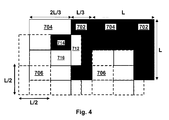
However, the resolution of a display formed from the color pixel shown in FIG. 3 is not limited to the resolution (L in both dimensions) of the color pixel itself. As illustrated in FIG. 4, by careful choice of size and placement of the pixel electrodes in the backplane, it is possible to produce a display having twice the resolution (i.e., L/2 in both dimensions) of the color pixel itself.
FIG. 4 shows two color pixels of the type shown in FIG. 3 formed side-by-side. A single backplane pixel comprising sub-pixel electrodes 712, 714 and 716 is illustrated with the sub-pixel electrodes shaded; seven additional adjacent backplane pixels are delimited by broken lines.
As may readily be seen from FIG. 4, each backplane pixel is L/2 square, and comprises a first sub-pixel electrode 712 which overlaps one-fourth of the area of the first sub-pixel 702, a second sub-pixel electrode 714 which overlaps one-fourth of the area of the second sub-pixel 704, and a third sub-pixel electrode 716 which overlaps one-fourth of the area of the third sub-pixel 706. The three sub-pixel electrodes 712, 714 and 716 have the same shapes and orientations as the corresponding sub-pixels 702, 704 and 706 respectively, but are one-half the size so that, as shown in FIG. 4, the second sub-pixel electrode 714 covers the lower right quadrant of sub-pixel 704, and the third sub-pixel electrode 716 covers the upper right quadrant of sub-pixel 706, while the first sub-pixel electrode 712 covers part of the first sub-pixel 702 lying in the left-hand half of sub-pixel 702 and extending for a distance L/4 in each direction from the horizontal plane of symmetry of sub-pixel 702.
It will be seen from FIG. 4 that sub-pixel 714 has two neighboring sub-pixels of the same color (the sub-pixels along its top and left edges, as illustrated in FIG. 4), sub-pixel 716 has two neighboring sub-pixels of the same color (the sub-pixels along its left and bottom edges), and sub-pixel 712 has three neighboring sub-pixels of the same color (the sub-pixels along its top, right and bottom edges).
It should be noted that the pixel electrode immediately below the pixel electrode 712, 714, 716 has its sub-pixel electrodes arranged in the same manner as the sub-pixel electrodes 712, 714 and 716, whereas the pixel electrodes immediately to the left and right of the pixel electrode 712, 714, 716 have their sub-pixel electrodes laterally reversed relative to the sub-pixel electrodes 712, 714 and 716.
Thus, in the display shown in FIG. 4, the size of the areas having the same color differs from those of the sub-pixel electrodes. The present invention is not, however, restricted to color displays prepared in this manner but extends generally to color displays having this characteristic.
A preferred display of this type is illustrated in FIG. 5. The display (generally designated 800) shown in FIG. 5 is a tetrachromatic color display having red, green, blue and white sub-pixels formed by a color filter array overlying a monochrome electro-optic medium. The individual colored areas (designated R, G, B and W respectively) of the color filter array each cover a 2×2 array of sub-pixel electrodes 802. Each color pixel of the display is formed from one-fourth of each of a red, green, blue and white colored area. For example, a color pixel 804 is outlined by a heavy square in FIG. 5. This colored pixel comprises the lower right-hand quadrant of a green colored area G, the lower left-hand quadrant of a red colored area R, the upper right-hand quadrant of a white “colored” area W and the upper left quadrant of a blue colored area B. Thus, a colored pixel is formed at every intersection of the color filter array at which red, green, blue, and white areas come together, and the four sub-pixels in each such colored pixel can be individually controlled since each sub-pixel overlies a single backplane sub-pixel electrode 802. It will be seen from FIG. 5 that each of the sub-pixels has neighboring sub-pixels of the same color along two of its adjacent edges.
FIGS. 6 and 7 illustrate the manner in which edge effects affect the color rendering of a display similar to that shown in FIG. 5, and explain why the display of FIG. 5 reduces such edge effects. For purposes of illustration, FIG. 6 shows a section of a color display in which red, green and blue sub-pixels of a color filter overlie a monochrome electro-optic medium 812, the sub-pixel areas of the electro-optic medium being switchable between their dark and light states by sub-pixel electrodes 814R, 814G and 814B respectively provided on a backplane (not shown).
FIG. 6 illustrates the section of the display shown set to a “green” state, in which the electrode 814G is set to cause the overlying section of the electro-optic medium 812 to appear white, while the electrodes 814R and 814B are set to cause the overlying sections of the electro-optic medium 812 to their dark states. Thus, when a ray 816 enters the display via a central section of the green sub-pixel of the color filter, this ray 816 passes through the green sub-pixel, is reflected from the light state electro-optic medium beneath, and passes back through the green sub-pixel of the color filter to be perceived by an observer as a green ray. (The manner in which ray 816 and the other rays shown in FIG. 6 are drawn is not intended to imply that reflection from the electro-optic medium is specular. Many electro-optic media, such as electrophoretic and electrochromic media, reflect in a Lambertian manner. However, the essential argument being regard to FIG. 6 is not affected by the difference between specular and Lambertian reflection.) However, consider a ray such as 818, which strikes the blue sub-pixel of the display, passes through this blue sub-pixel, strikes a peripheral portion of the light state electro-optic medium, and passes out of through the green sub-pixel. The effect of rays such as 818 is to make a peripheral area of the green sub-pixel adjacent the blue sub-pixel appear bluish green, as illustrated in FIG. 7. This is the aforementioned edge effect.
(It might at first glance appear that a ray, such as ray 818 in FIG. 6, which passed through both blue and green portions of the color filter would be completely absorbed by the color filter and would not produce the edge effect discussed above. While this is theoretically the case, the color filters used in electro-optic displays do not have completely saturated colors, i.e., the red portions of the color filter pass some green and some blue light, since using anything approaching completely saturated colors would render white areas of the display too dark. Hence, some of the blue light emerging from the blue sub-pixel does pass through the green sub-pixel leading to the edge effect noted above.)
Similar edge effects are produced by rays such as ray 820 in FIG. 6, which pass through the green sub-pixel, are reflected from the light electro-optic medium, and pass out through the red sub-pixel. In this case, the edge effect takes the form of a greenish-red color in a portion of the red sub-pixel adjacent the green sub-pixel.
FIG. 7 shows, in a highly schematic manner, the edge effects associated with the one sub-pixel located in the center of the Figure, and doe not show the edge effects associated with the other illustrated sub-pixels. Furthermore, FIG. 7 makes no attempt to illustrate the different color actually produced by the edge effects, only the areas affected. It will be seen from FIG. 7 that the result of the edge effects is to leave the central area of the sub-pixel displaying its intended color while a peripheral area, which may extend over the whole periphery of the sub-pixel. The edge effects are also responsible for color distortion in narrow strips along the edges of the other sub-pixels which share a common edge with the central sub-pixel.
It will readily be apparent from the foregoing explanation of the origin of edge effects that the color distortion caused by the edge effects only occurs at edges between sub-pixels of different colors. For example, if both the center and right-hand sub-pixels shown in FIG. 6 were green, rays such as ray 818 in FIG. 6 would not cause any color distortion along the edge between the two sub-pixels. Rays similar to ray 820 will cause a slight distortion of the size of the sub-pixel, since they will cause some green to appear outside the area of the relevant sub-pixel, but they will not cause color distortion.
In the display shown in FIG. 5, the edge effects are minimized because each colored sub-pixel has two of its four neighbors of the same color as itself, so that edge effects occur at only one-half of the edges between adjacent sub-pixels. The effective resolution of the display is increased to improve font rendering and for other purposes, but the color gamut is not reduced by increased edge effects.
This aspect of the present invention is not restricted to color displays using color filter arrays, but is also applicable to certain type of inherent color display. For example U.S. Pat. No. 6,933,098 describes an inherent microcell electrophoretic display which uses a single type of white electrophoretic particle suspending in the differently dyed liquids, the liquid being contained in separate microcells. Switching of this display is effected by moving the electrophoretic particles between a position adjacent a viewing surface (which causes the microcell to appear white) and a position remote from the viewing surface (which causes incident light to pass through the colored fluid, be reflected from the white electrophoretic particles and pass back through the fluid, so that the microcell takes on the color of the fluid). Thus each microcell, and hence each sub-pixel containing one or more microcells, is capable of displaying white and one other color. Other variations of inherent color displays use sub-pixels capable of displaying one selected color plus black. It should readily be apparent that both these type of inherent color display can suffer from edge effects produced in a manner very similar to those explained above with reference to FIGS. 6 and 7, and hence that modifying such a display in accordance with the present invention can produce useful improvement in the electro-optic characteristics of the display.
It will be apparent to those skilled in the technology of electro-optic displays that modification of color electro-optic displays in accordance with the present invention will require changes in the methods used to render images from outside sources (such as digital photographs) on the display. The presently preferred method is to process the image at the full resolution of the TFT and the corresponding color information is calculated from a neighborhood and reduced to the underlying CFA color only at the final step of the process.
Numerous changes and modifications can be made in the preferred embodiments of the present invention already described without departing from the spirit and skill of the invention. Accordingly, the foregoing description is to be construed in an illustrative and not in a limitative sense.

Claims (11)

The invention claimed is:
1. A color display having areas of at least three different colors, the areas of different colors forming continuous areas of a single color each covering a plurality of sub-pixel electrodes, the continuous areas of a single color and the sub-pixel electrodes being arranged such that the sub-pixels are rectangular and each sub-pixel of a given color has sub-pixels of the same given color disposed along at least two of its adjacent edges; the color display having continuous areas of three different colors, the continuous areas of a first color having the form of a series of spaced parallel stripes and the continuous areas of the second and third colors having the form of alternating rectangles of the second and third colors disposed in the spaces between the spaced parallel stripes of the first color.
2. A color display according to claim 1 having continuous areas of four different colors, each continuous area of a single color covering a 2×2 array of sub-pixel electrodes.
3. A color display according to claim 1 having red, green and blue colored areas.
4. A color display according to claim 1 having orange, lime and purple colored areas.
5. A color display according to claim 1 comprising a color filter array superposed on an electro-optic medium having light and dark optical states.
6. A color display according to claim 1 wherein the plurality of colored areas are provided by a plurality of differing electrophoretic media, whereby each of the differing electrophoretic media is capable of displaying at least one of white and black, and a color other than black or white.
7. A color display according to claim 1 comprising an electrophoretic material comprising a plurality of electrically charged particles disposed in a fluid and capable of moving through the fluid under the influence of an electric field.
8. A color display according to claim 7 wherein the electrically charged particles and the fluid are confined within a plurality of capsules or micro cells.
9. A color display according to claim 7 wherein the electrically charged particles and the fluid are present as a plurality of discrete droplets surrounded by a continuous phase comprising a polymeric material.
10. A color display according to claim 7 wherein the fluid is gaseous.
11. An electronic book reader, portable computer, tablet computer, cellular telephone, smart card, sign, watch, shelf label or flash drive comprising a display according to claim 1.
US13/032,914 2007-08-03 2011-02-23 Electro-optic displays, and processes for their production Active 2028-10-10 US8902153B2 (en)

Priority Applications (1)

Application Number Priority Date Filing Date Title
US13/032,914 US8902153B2 (en) 2007-08-03 2011-02-23 Electro-optic displays, and processes for their production

Applications Claiming Priority (2)

Application Number Priority Date Filing Date Title
US11/833,578 US7910175B2 (en) 2003-03-25 2007-08-03 Processes for the production of electrophoretic displays
US13/032,914 US8902153B2 (en) 2007-08-03 2011-02-23 Electro-optic displays, and processes for their production

Related Parent Applications (1)

Application Number Title Priority Date Filing Date
US11/833,578 Continuation-In-Part US7910175B2 (en) 2003-03-25 2007-08-03 Processes for the production of electrophoretic displays

Publications (2)

Publication Number Publication Date
US20110310461A1 US20110310461A1 (en) 2011-12-22
US8902153B2 true US8902153B2 (en) 2014-12-02

Family

ID=45328428

Family Applications (1)

Application Number Title Priority Date Filing Date
US13/032,914 Active 2028-10-10 US8902153B2 (en) 2007-08-03 2011-02-23 Electro-optic displays, and processes for their production

Country Status (1)

Country Link
US (1) US8902153B2 (en)

Cited By (55)

* Cited by examiner, † Cited by third party
Publication number Priority date Publication date Assignee Title
US20150109658A1 (en) * 2013-10-18 2015-04-23 E Ink Holdings Inc. Electrophoretic display apparatus
US9361836B1 (en) 2013-12-20 2016-06-07 E Ink Corporation Aggregate particles for use in electrophoretic color displays
US9436056B2 (en) 2013-02-06 2016-09-06 E Ink Corporation Color electro-optic displays
US9697778B2 (en) 2013-05-14 2017-07-04 E Ink Corporation Reverse driving pulses in electrophoretic displays
US9752034B2 (en) 2015-11-11 2017-09-05 E Ink Corporation Functionalized quinacridone pigments
US9761181B2 (en) 2014-07-09 2017-09-12 E Ink California, Llc Color display device
US9904139B2 (en) * 2016-03-18 2018-02-27 Boe Technology Group Co., Ltd. Color filter substrate, display panel and display device
US9921451B2 (en) 2014-09-10 2018-03-20 E Ink Corporation Colored electrophoretic displays
US9922603B2 (en) 2014-07-09 2018-03-20 E Ink California, Llc Color display device and driving methods therefor
US10036931B2 (en) 2014-01-14 2018-07-31 E Ink California, Llc Color display device
US10040954B2 (en) 2015-05-28 2018-08-07 E Ink California, Llc Electrophoretic medium comprising a mixture of charge control agents
US10062337B2 (en) 2015-10-12 2018-08-28 E Ink California, Llc Electrophoretic display device
WO2018164942A1 (en) 2017-03-06 2018-09-13 E Ink Corporation Method for rendering color images
US10087344B2 (en) 2015-10-30 2018-10-02 E Ink Corporation Methods for sealing microcell containers with phenethylamine mixtures
US10175550B2 (en) 2014-11-07 2019-01-08 E Ink Corporation Applications of electro-optic displays
US10254619B2 (en) 2013-05-17 2019-04-09 E Ink California, Llc Driving methods for color display devices
US10254620B1 (en) 2016-03-08 2019-04-09 E Ink Corporation Encapsulated photoelectrophoretic display
US10270939B2 (en) 2016-05-24 2019-04-23 E Ink Corporation Method for rendering color images
US10276109B2 (en) 2016-03-09 2019-04-30 E Ink Corporation Method for driving electro-optic displays
US10353266B2 (en) 2014-09-26 2019-07-16 E Ink Corporation Color sets for low resolution dithering in reflective color displays
US10380955B2 (en) 2014-07-09 2019-08-13 E Ink California, Llc Color display device and driving methods therefor
US10444592B2 (en) 2017-03-09 2019-10-15 E Ink Corporation Methods and systems for transforming RGB image data to a reduced color set for electro-optic displays
US10573257B2 (en) 2017-05-30 2020-02-25 E Ink Corporation Electro-optic displays
US10593272B2 (en) 2016-03-09 2020-03-17 E Ink Corporation Drivers providing DC-balanced refresh sequences for color electrophoretic displays
US10657869B2 (en) 2014-09-10 2020-05-19 E Ink Corporation Methods for driving color electrophoretic displays
US10782586B2 (en) 2017-01-20 2020-09-22 E Ink California, Llc Color organic pigments and electrophoretic display media containing the same
US10891906B2 (en) 2014-07-09 2021-01-12 E Ink California, Llc Color display device and driving methods therefor
US11079651B2 (en) 2017-12-15 2021-08-03 E Ink Corporation Multi-color electro-optic media
US11087644B2 (en) 2015-08-19 2021-08-10 E Ink Corporation Displays intended for use in architectural applications
US11098206B2 (en) 2015-10-06 2021-08-24 E Ink Corporation Electrophoretic media including charge control agents comprising quartenary amines and unsaturated polymeric tails
US11143929B2 (en) 2018-03-09 2021-10-12 E Ink Corporation Reflective electrophoretic displays including photo-luminescent material and color filter arrays
US11248122B2 (en) 2017-12-30 2022-02-15 E Ink Corporation Pigments for electrophoretic displays
US11266832B2 (en) 2017-11-14 2022-03-08 E Ink California, Llc Electrophoretic active delivery system including porous conductive electrode layer
US11287718B2 (en) 2015-08-04 2022-03-29 E Ink Corporation Reusable display addressable with incident light
US11404013B2 (en) 2017-05-30 2022-08-02 E Ink Corporation Electro-optic displays with resistors for discharging remnant charges
US11422427B2 (en) 2017-12-19 2022-08-23 E Ink Corporation Applications of electro-optic displays
US11460165B2 (en) 2012-04-20 2022-10-04 E Ink Corporation Illumination systems for reflective displays
US11460722B2 (en) 2019-05-10 2022-10-04 E Ink Corporation Colored electrophoretic displays
US11467466B2 (en) 2012-04-20 2022-10-11 E Ink Corporation Illumination systems for reflective displays
WO2023043714A1 (en) 2021-09-14 2023-03-23 E Ink Corporation Coordinated top electrode - drive electrode voltages for switching optical state of electrophoretic displays using positive and negative voltages of different magnitudes
US11620959B2 (en) 2020-11-02 2023-04-04 E Ink Corporation Enhanced push-pull (EPP) waveforms for achieving primary color sets in multi-color electrophoretic displays
US11640803B2 (en) 2021-09-06 2023-05-02 E Ink California, Llc Method for driving electrophoretic display device
US11686989B2 (en) 2020-09-15 2023-06-27 E Ink Corporation Four particle electrophoretic medium providing fast, high-contrast optical state switching
WO2023132958A1 (en) 2022-01-04 2023-07-13 E Ink Corporation Electrophoretic media comprising electrophoretic particles and a combination of charge control agents
US11721296B2 (en) 2020-11-02 2023-08-08 E Ink Corporation Method and apparatus for rendering color images
US11756494B2 (en) 2020-11-02 2023-09-12 E Ink Corporation Driving sequences to remove prior state information from color electrophoretic displays
US11776496B2 (en) 2020-09-15 2023-10-03 E Ink Corporation Driving voltages for advanced color electrophoretic displays and displays with improved driving voltages
WO2023211867A1 (en) 2022-04-27 2023-11-02 E Ink Corporation Color displays configured to convert rgb image data for display on advanced color electronic paper
US11846863B2 (en) 2020-09-15 2023-12-19 E Ink Corporation Coordinated top electrode—drive electrode voltages for switching optical state of electrophoretic displays using positive and negative voltages of different magnitudes
US11869451B2 (en) 2021-11-05 2024-01-09 E Ink Corporation Multi-primary display mask-based dithering with low blooming sensitivity
US11868020B2 (en) 2020-06-05 2024-01-09 E Ink Corporation Electrophoretic display device
WO2024044119A1 (en) 2022-08-25 2024-02-29 E Ink Corporation Transitional driving modes for impulse balancing when switching between global color mode and direct update mode for electrophoretic displays
US11922893B2 (en) 2021-12-22 2024-03-05 E Ink Corporation High voltage driving using top plane switching with zero voltage frames between driving frames
US11935495B2 (en) 2021-08-18 2024-03-19 E Ink Corporation Methods for driving electro-optic displays
US11938214B2 (en) 2019-11-27 2024-03-26 E Ink Corporation Benefit agent delivery system comprising microcells having an electrically eroding sealing layer

Families Citing this family (11)

* Cited by examiner, † Cited by third party
Publication number Priority date Publication date Assignee Title
DE69934618T2 (en) 1998-07-08 2007-05-03 E-Ink Corp., Cambridge Improved colored microencapsulated electrophoretic display
KR100941415B1 (en) * 2007-10-23 2010-02-10 삼성전자주식회사 Liquid barcode and liquid barcode reader
JP5628156B2 (en) * 2008-06-17 2014-11-19 コーニンクレッカ フィリップス エヌ ヴェ Appearance changing device, method of manufacturing such a device, and equipment covered by such a device
JP5449617B2 (en) 2010-04-02 2014-03-19 イー インク コーポレイション Electrophoresis medium
US9122143B2 (en) 2012-06-07 2015-09-01 Mindflow Llc Dynamically variable graphic material using electrostatically attracted particles
US9195111B2 (en) 2013-02-11 2015-11-24 E Ink Corporation Patterned electro-optic displays and processes for the production thereof
JP6191178B2 (en) 2013-03-18 2017-09-06 セイコーエプソン株式会社 Electro-optical device, electronic apparatus, and control method of electro-optical device
GB2519777B (en) * 2013-10-30 2020-06-17 Flexenable Ltd Display systems and methods
JP6651467B2 (en) 2014-06-17 2020-02-19 セイジ・エレクトロクロミクス,インコーポレイテッド Controlled switching of electrochromic devices
CN106229300B (en) * 2016-08-23 2019-03-22 武汉华星光电技术有限公司 Dot structure and production method
CN113168005B (en) 2018-12-13 2023-05-02 伊英克公司 Illumination system for reflective display

Citations (202)

* Cited by examiner, † Cited by third party
Publication number Priority date Publication date Assignee Title
US4418346A (en) 1981-05-20 1983-11-29 Batchelder J Samuel Method and apparatus for providing a dielectrophoretic display of visual information
US5760761A (en) 1995-12-15 1998-06-02 Xerox Corporation Highlight color twisting ball display
US5777782A (en) 1996-12-24 1998-07-07 Xerox Corporation Auxiliary optics for a twisting ball display
US5808783A (en) 1996-06-27 1998-09-15 Xerox Corporation High reflectance gyricon display
US5872552A (en) 1994-12-28 1999-02-16 International Business Machines Corporation Electrophoretic display
US5930026A (en) 1996-10-25 1999-07-27 Massachusetts Institute Of Technology Nonemissive displays and piezoelectric power supplies therefor
US5961804A (en) 1997-03-18 1999-10-05 Massachusetts Institute Of Technology Microencapsulated electrophoretic display
US6017584A (en) 1995-07-20 2000-01-25 E Ink Corporation Multi-color electrophoretic displays and materials for making the same
US6054071A (en) 1998-01-28 2000-04-25 Xerox Corporation Poled electrets for gyricon-based electric-paper displays
US6055091A (en) 1996-06-27 2000-04-25 Xerox Corporation Twisting-cylinder display
US6067185A (en) 1997-08-28 2000-05-23 E Ink Corporation Process for creating an encapsulated electrophoretic display
WO2000036560A1 (en) 1998-12-18 2000-06-22 E Ink Corporation Electronic ink display media for security and authentication
WO2000038000A1 (en) 1998-12-22 2000-06-29 E Ink Corporation Method of manufacturing of a discrete electronic device
US6097531A (en) 1998-11-25 2000-08-01 Xerox Corporation Method of making uniformly magnetized elements for a gyricon display
US6118426A (en) 1995-07-20 2000-09-12 E Ink Corporation Transducers and indicators having printed displays
US6120588A (en) 1996-07-19 2000-09-19 E Ink Corporation Electronically addressable microencapsulated ink and display thereof
US6120839A (en) 1995-07-20 2000-09-19 E Ink Corporation Electro-osmotic displays and materials for making the same
US6124851A (en) 1995-07-20 2000-09-26 E Ink Corporation Electronic book with multiple page displays
US6128124A (en) 1998-10-16 2000-10-03 Xerox Corporation Additive color electric paper without registration or alignment of individual elements
US6130774A (en) 1998-04-27 2000-10-10 E Ink Corporation Shutter mode microencapsulated electrophoretic display
US6137467A (en) 1995-01-03 2000-10-24 Xerox Corporation Optically sensitive electric paper
US6144361A (en) 1998-09-16 2000-11-07 International Business Machines Corporation Transmissive electrophoretic display with vertical electrodes
WO2000067110A1 (en) 1999-05-03 2000-11-09 E Ink Corporation Display unit for electronic shelf price label system
US6147791A (en) 1998-11-25 2000-11-14 Xerox Corporation Gyricon displays utilizing rotating elements and magnetic latching
US6177921B1 (en) 1997-08-28 2001-01-23 E Ink Corporation Printable electrode structures for displays
WO2001007961A1 (en) 1999-07-21 2001-02-01 E Ink Corporation Use of a storage capacitor to enhance the performance of an active matrix driven electronic display
US6184856B1 (en) 1998-09-16 2001-02-06 International Business Machines Corporation Transmissive electrophoretic display with laterally adjacent color cells
US6225971B1 (en) 1998-09-16 2001-05-01 International Business Machines Corporation Reflective electrophoretic display with laterally adjacent color cells using an absorbing panel
US6232950B1 (en) 1997-08-28 2001-05-15 E Ink Corporation Rear electrode structures for displays
US6249271B1 (en) 1995-07-20 2001-06-19 E Ink Corporation Retroreflective electrophoretic displays and materials for making the same
US6252564B1 (en) 1997-08-28 2001-06-26 E Ink Corporation Tiled displays
US6262706B1 (en) 1995-07-20 2001-07-17 E Ink Corporation Retroreflective electrophoretic displays and materials for making the same
US6262833B1 (en) 1998-10-07 2001-07-17 E Ink Corporation Capsules for electrophoretic displays and methods for making the same
US6271823B1 (en) 1998-09-16 2001-08-07 International Business Machines Corporation Reflective electrophoretic display with laterally adjacent color cells using a reflective panel
US6301038B1 (en) 1997-02-06 2001-10-09 University College Dublin Electrochromic system
US6300932B1 (en) 1997-08-28 2001-10-09 E Ink Corporation Electrophoretic displays with luminescent particles and materials for making the same
US6312971B1 (en) 1999-08-31 2001-11-06 E Ink Corporation Solvent annealing process for forming a thin semiconductor film with advantageous properties
US6312304B1 (en) 1998-12-15 2001-11-06 E Ink Corporation Assembly of microencapsulated electronic displays
US6323989B1 (en) 1996-07-19 2001-11-27 E Ink Corporation Electrophoretic displays using nanoparticles
US6327072B1 (en) 1999-04-06 2001-12-04 E Ink Corporation Microcell electrophoretic displays
EP1099207B1 (en) 1998-07-22 2002-03-27 E-Ink Corporation Electronic display
US6377387B1 (en) 1999-04-06 2002-04-23 E Ink Corporation Methods for producing droplets for use in capsule-based electrophoretic displays
US6376828B1 (en) 1998-10-07 2002-04-23 E Ink Corporation Illumination system for nonemissive electronic displays
US6392786B1 (en) 1999-07-01 2002-05-21 E Ink Corporation Electrophoretic medium provided with spacers
US20020060321A1 (en) 2000-07-14 2002-05-23 Kazlas Peter T. Minimally- patterned, thin-film semiconductor devices for display applications
US6413790B1 (en) 1999-07-21 2002-07-02 E Ink Corporation Preferred methods for producing electrical circuit elements used to control an electronic display
US20020090980A1 (en) 2000-12-05 2002-07-11 Wilcox Russell J. Displays for portable electronic apparatus
US6445489B1 (en) 1998-03-18 2002-09-03 E Ink Corporation Electrophoretic displays and systems for addressing such displays
US6459418B1 (en) 1995-07-20 2002-10-01 E Ink Corporation Displays combining active and non-active inks
US6473072B1 (en) 1998-05-12 2002-10-29 E Ink Corporation Microencapsulated electrophoretic electrostatically-addressed media for drawing device applications
US6480182B2 (en) 1997-03-18 2002-11-12 Massachusetts Institute Of Technology Printable electronic display
US6498114B1 (en) 1999-04-09 2002-12-24 E Ink Corporation Method for forming a patterned semiconductor film
US6504524B1 (en) 2000-03-08 2003-01-07 E Ink Corporation Addressing methods for displays having zero time-average field
US6506438B2 (en) 1998-12-15 2003-01-14 E Ink Corporation Method for printing of transistor arrays on plastic substrates
US6512354B2 (en) 1998-07-08 2003-01-28 E Ink Corporation Method and apparatus for sensing the state of an electrophoretic display
US6515649B1 (en) 1995-07-20 2003-02-04 E Ink Corporation Suspended particle displays and materials for making the same
US6518949B2 (en) 1998-04-10 2003-02-11 E Ink Corporation Electronic displays using organic-based field effect transistors
US6531997B1 (en) 1999-04-30 2003-03-11 E Ink Corporation Methods for addressing electrophoretic displays
US6538801B2 (en) 1996-07-19 2003-03-25 E Ink Corporation Electrophoretic displays using nanoparticles
US6545291B1 (en) 1999-08-31 2003-04-08 E Ink Corporation Transistor design for use in the construction of an electronically driven display
EP1145072B1 (en) 1998-06-22 2003-05-07 E-Ink Corporation Method of addressing microencapsulated display media
US20030102858A1 (en) 1998-07-08 2003-06-05 E Ink Corporation Method and apparatus for determining properties of an electrophoretic display
US6580545B2 (en) 2001-04-19 2003-06-17 E Ink Corporation Electrochromic-nanoparticle displays
US6639578B1 (en) 1995-07-20 2003-10-28 E Ink Corporation Flexible displays
US6657772B2 (en) 2001-07-09 2003-12-02 E Ink Corporation Electro-optic display and adhesive composition for use therein
US6664944B1 (en) 1995-07-20 2003-12-16 E-Ink Corporation Rear electrode structures for electrophoretic displays
US6693620B1 (en) 1999-05-03 2004-02-17 E Ink Corporation Threshold addressing of electrophoretic displays
US6704133B2 (en) 1998-03-18 2004-03-09 E-Ink Corporation Electro-optic display overlays and systems for addressing such displays
US6710540B1 (en) 1995-07-20 2004-03-23 E Ink Corporation Electrostatically-addressable electrophoretic display
US6721083B2 (en) 1996-07-19 2004-04-13 E Ink Corporation Electrophoretic displays using nanoparticles
US6724519B1 (en) 1998-12-21 2004-04-20 E-Ink Corporation Protective electrodes for electrophoretic displays
US6727881B1 (en) 1995-07-20 2004-04-27 E Ink Corporation Encapsulated electrophoretic displays and methods and materials for making the same
US20040105036A1 (en) 2002-08-06 2004-06-03 E Ink Corporation Protection of electro-optic displays against thermal effects
US6753999B2 (en) 1998-03-18 2004-06-22 E Ink Corporation Electrophoretic displays in portable devices and systems for addressing such displays
US20040119681A1 (en) 1998-11-02 2004-06-24 E Ink Corporation Broadcast system for electronic ink signs
US20040155857A1 (en) * 2002-09-03 2004-08-12 E Ink Corporation Electro-optic displays
WO2004079442A1 (en) 2003-03-06 2004-09-16 Bridgestone Corporation Production method for iamge display unit and image display unit
US6816147B2 (en) 2000-08-17 2004-11-09 E Ink Corporation Bistable electro-optic display, and method for addressing same
US6819471B2 (en) 2001-08-16 2004-11-16 E Ink Corporation Light modulation by frustration of total internal reflection
US6822782B2 (en) 2001-05-15 2004-11-23 E Ink Corporation Electrophoretic particles and processes for the production thereof
US6825970B2 (en) 2001-09-14 2004-11-30 E Ink Corporation Methods for addressing electro-optic materials
US6825829B1 (en) 1997-08-28 2004-11-30 E Ink Corporation Adhesive backed displays
US6825068B2 (en) 2000-04-18 2004-11-30 E Ink Corporation Process for fabricating thin film transistors
US6831769B2 (en) 2001-07-09 2004-12-14 E Ink Corporation Electro-optic display and lamination adhesive
US6839158B2 (en) 1997-08-28 2005-01-04 E Ink Corporation Encapsulated electrophoretic displays having a monolayer of capsules and materials and methods for making the same
US20050001810A1 (en) 2001-09-19 2005-01-06 Gaku Yakushiji Particles and device for displaying image
US6842279B2 (en) 2002-06-27 2005-01-11 E Ink Corporation Illumination system for nonemissive electronic displays
US6842657B1 (en) 1999-04-09 2005-01-11 E Ink Corporation Reactive formation of dielectric layers and protection of organic layers in organic semiconductor device fabrication
US20050012980A1 (en) 2003-05-02 2005-01-20 E Ink Corporation Electrophoretic displays with controlled amounts of pigment
US6865010B2 (en) 2001-12-13 2005-03-08 E Ink Corporation Electrophoretic electronic displays with low-index films
US6864875B2 (en) 1998-04-10 2005-03-08 E Ink Corporation Full color reflective display with multichromatic sub-pixels
US6866760B2 (en) 1998-08-27 2005-03-15 E Ink Corporation Electrophoretic medium and process for the production thereof
US6870661B2 (en) 2001-05-15 2005-03-22 E Ink Corporation Electrophoretic displays containing magnetic particles
US6870657B1 (en) 1999-10-11 2005-03-22 University College Dublin Electrochromic device
US6900851B2 (en) 2002-02-08 2005-05-31 E Ink Corporation Electro-optic displays and optical systems for addressing such displays
US20050122306A1 (en) 2003-10-29 2005-06-09 E Ink Corporation Electro-optic displays with single edge addressing and removable driver circuitry
US20050122563A1 (en) 2003-07-24 2005-06-09 E Ink Corporation Electro-optic displays
US20050122284A1 (en) 2003-11-25 2005-06-09 E Ink Corporation Electro-optic displays, and methods for driving same
US20050156340A1 (en) 2004-01-20 2005-07-21 E Ink Corporation Preparation of capsules
US6922276B2 (en) 2002-12-23 2005-07-26 E Ink Corporation Flexible electro-optic displays
US6933098B2 (en) 2000-01-11 2005-08-23 Sipix Imaging Inc. Process for roll-to-roll manufacture of a display by synchronized photolithographic exposure on a substrate web
US6950220B2 (en) 2002-03-18 2005-09-27 E Ink Corporation Electro-optic displays, and methods for driving same
US6958848B2 (en) 2002-05-23 2005-10-25 E Ink Corporation Capsules, materials for use therein and electrophoretic media and displays containing such capsules
US20050253777A1 (en) 2004-05-12 2005-11-17 E Ink Corporation Tiled displays and methods for driving same
US6967640B2 (en) 2001-07-27 2005-11-22 E Ink Corporation Microencapsulated electrophoretic display with integrated driver
US20050259068A1 (en) 2001-12-10 2005-11-24 Norio Nihei Image display
US6982178B2 (en) 2002-06-10 2006-01-03 E Ink Corporation Components and methods for use in electro-optic displays
US6987603B2 (en) 2003-01-31 2006-01-17 E Ink Corporation Construction of electrophoretic displays
US7002728B2 (en) 1997-08-28 2006-02-21 E Ink Corporation Electrophoretic particles, and processes for the production thereof
US7012600B2 (en) 1999-04-30 2006-03-14 E Ink Corporation Methods for driving bistable electro-optic displays, and apparatus for use therein
US7012735B2 (en) 2003-03-27 2006-03-14 E Ink Corporaiton Electro-optic assemblies, and materials for use therein
US7023420B2 (en) 2000-11-29 2006-04-04 E Ink Corporation Electronic display with photo-addressing means
US7030854B2 (en) 2001-03-13 2006-04-18 E Ink Corporation Apparatus for displaying drawings
US7030412B1 (en) 1999-05-05 2006-04-18 E Ink Corporation Minimally-patterned semiconductor devices for display applications
US7034783B2 (en) 2003-08-19 2006-04-25 E Ink Corporation Method for controlling electro-optic display
US20060087718A1 (en) 2002-04-26 2006-04-27 Bridgestone Corporation Particle for image display and its apparatus
US20060087479A1 (en) 2002-06-21 2006-04-27 Bridgestone Corporation Image display and method for manufacturing image display
US20060087489A1 (en) 2002-07-17 2006-04-27 Ryou Sakurai Image display
US7038655B2 (en) 1999-05-03 2006-05-02 E Ink Corporation Electrophoretic ink composed of particles with field dependent mobilities
US7071913B2 (en) 1995-07-20 2006-07-04 E Ink Corporation Retroreflective electrophoretic displays and materials for making the same
US7075703B2 (en) 2004-01-16 2006-07-11 E Ink Corporation Process for sealing electro-optic displays
US7079305B2 (en) 2001-03-19 2006-07-18 E Ink Corporation Electrophoretic medium and process for the production thereof
US20060181504A1 (en) 2005-02-17 2006-08-17 Seiko Epson Corporation Electrophoresis device, method of driving electrophoresis device, and electronic apparatus
US7110163B2 (en) 2001-07-09 2006-09-19 E Ink Corporation Electro-optic display and lamination adhesive for use therein
US7110164B2 (en) 2002-06-10 2006-09-19 E Ink Corporation Electro-optic displays, and processes for the production thereof
US7109968B2 (en) 1995-07-20 2006-09-19 E Ink Corporation Non-spherical cavity electrophoretic displays and methods and materials for making the same
US20060209008A1 (en) 2002-04-17 2006-09-21 Bridgestone Corporation Image display device
US20060214906A1 (en) 2002-12-24 2006-09-28 Bridgestone Corporation Image display
US7116318B2 (en) 2002-04-24 2006-10-03 E Ink Corporation Backplanes for display applications, and components for use therein
US7116466B2 (en) 2004-07-27 2006-10-03 E Ink Corporation Electro-optic displays
US7119772B2 (en) 1999-04-30 2006-10-10 E Ink Corporation Methods for driving bistable electro-optic displays, and apparatus for use therein
US7119759B2 (en) 1999-05-03 2006-10-10 E Ink Corporation Machine-readable displays
US20060231401A1 (en) 2002-12-17 2006-10-19 Ryou Sakurai Image display panel manufacturing method, image display device manufacturing method, and image disiplay device
US7167155B1 (en) 1995-07-20 2007-01-23 E Ink Corporation Color electrophoretic displays
US7170670B2 (en) 2001-04-02 2007-01-30 E Ink Corporation Electrophoretic medium and display with improved image stability
US7173752B2 (en) 2003-11-05 2007-02-06 E Ink Corporation Electro-optic displays, and materials for use therein
US20070052757A1 (en) 1996-07-19 2007-03-08 E Ink Corporation Electronically addressable microencapsulated ink and display thereof
US7190008B2 (en) 2002-04-24 2007-03-13 E Ink Corporation Electro-optic displays, and components for use therein
US7193625B2 (en) 1999-04-30 2007-03-20 E Ink Corporation Methods for driving electro-optic displays, and apparatus for use therein
US7202847B2 (en) 2002-06-28 2007-04-10 E Ink Corporation Voltage modulated driver circuits for electro-optic displays
US7206119B2 (en) 2003-12-31 2007-04-17 E Ink Corporation Electro-optic displays, and method for driving same
US20070091417A1 (en) 2005-10-25 2007-04-26 E Ink Corporation Electrophoretic media and displays with improved binder
US7223672B2 (en) 2002-04-24 2007-05-29 E Ink Corporation Processes for forming backplanes for electro-optic displays
US7230751B2 (en) 2005-01-26 2007-06-12 E Ink Corporation Electrophoretic displays using gaseous fluids
US7230750B2 (en) 2001-05-15 2007-06-12 E Ink Corporation Electrophoretic media and processes for the production thereof
US7236290B1 (en) 2000-07-25 2007-06-26 E Ink Corporation Electrophoretic medium with improved stability
US7236291B2 (en) 2003-04-02 2007-06-26 Bridgestone Corporation Particle use for image display media, image display panel using the particles, and image display device
US7242513B2 (en) 1997-08-28 2007-07-10 E Ink Corporation Encapsulated electrophoretic displays having a monolayer of capsules and materials and methods for making the same
US7247379B2 (en) 1997-08-28 2007-07-24 E Ink Corporation Electrophoretic particles, and processes for the production thereof
US7256766B2 (en) 1998-08-27 2007-08-14 E Ink Corporation Electrophoretic display comprising optical biasing element
US7259744B2 (en) 1995-07-20 2007-08-21 E Ink Corporation Dielectrophoretic displays
US20070211002A1 (en) 2006-03-09 2007-09-13 E Ink Corporation Electro-optic display with edge seal
US7304634B2 (en) 1995-07-20 2007-12-04 E Ink Corporation Rear electrode structures for electrophoretic displays
US20070285385A1 (en) 1998-11-02 2007-12-13 E Ink Corporation Broadcast system for electronic ink signs
US7312916B2 (en) 2002-08-07 2007-12-25 E Ink Corporation Electrophoretic media containing specularly reflective particles
US7321459B2 (en) 2002-03-06 2008-01-22 Bridgestone Corporation Image display device and method
US20080024482A1 (en) 2002-06-13 2008-01-31 E Ink Corporation Methods for driving electro-optic displays
US20080024429A1 (en) 2006-07-25 2008-01-31 E Ink Corporation Electrophoretic displays using gaseous fluids
US7327511B2 (en) 2004-03-23 2008-02-05 E Ink Corporation Light modulators
US20080043318A1 (en) 2005-10-18 2008-02-21 E Ink Corporation Color electro-optic displays, and processes for the production thereof
US7339715B2 (en) 2003-03-25 2008-03-04 E Ink Corporation Processes for the production of electrophoretic displays
US7352353B2 (en) 1995-07-20 2008-04-01 E Ink Corporation Electrostatically addressable electrophoretic display
US7365733B2 (en) 2002-12-16 2008-04-29 E Ink Corporation Backplanes for electro-optic displays
US7369299B2 (en) 2003-02-25 2008-05-06 Bridgestone Corporation Image display panel and image display device
US7388572B2 (en) 2004-02-27 2008-06-17 E Ink Corporation Backplanes for electro-optic displays
US7411719B2 (en) 1995-07-20 2008-08-12 E Ink Corporation Electrophoretic medium and process for the production thereof
US7420549B2 (en) 2003-10-08 2008-09-02 E Ink Corporation Electro-wetting displays
US7453445B2 (en) 2004-08-13 2008-11-18 E Ink Corproation Methods for driving electro-optic displays
US7477444B2 (en) 2006-09-22 2009-01-13 E Ink Corporation & Air Products And Chemical, Inc. Electro-optic display and materials for use therein
US7492497B2 (en) 2006-08-02 2009-02-17 E Ink Corporation Multi-layer light modulator
US7492339B2 (en) 2004-03-26 2009-02-17 E Ink Corporation Methods for driving bistable electro-optic displays
US7528822B2 (en) 2001-11-20 2009-05-05 E Ink Corporation Methods for driving electro-optic displays
US7535624B2 (en) 2001-07-09 2009-05-19 E Ink Corporation Electro-optic display and materials for use therein
US7551346B2 (en) 2003-11-05 2009-06-23 E Ink Corporation Electro-optic displays, and materials for use therein
US7554712B2 (en) 2005-06-23 2009-06-30 E Ink Corporation Edge seals for, and processes for assembly of, electro-optic displays
US20090179842A1 (en) * 2008-01-10 2009-07-16 Industrial Technology Research Institute Flat display panel
US7583427B2 (en) 2002-06-10 2009-09-01 E Ink Corporation Components and methods for use in electro-optic displays
US7602374B2 (en) 2003-09-19 2009-10-13 E Ink Corporation Methods for reducing edge effects in electro-optic displays
US7649674B2 (en) 2002-06-10 2010-01-19 E Ink Corporation Electro-optic display with edge seal
US7667684B2 (en) 1998-07-08 2010-02-23 E Ink Corporation Methods for achieving improved color in microencapsulated electrophoretic devices
US7672040B2 (en) 2003-11-05 2010-03-02 E Ink Corporation Electro-optic displays, and materials for use therein
US7679814B2 (en) 2001-04-02 2010-03-16 E Ink Corporation Materials for use in electrophoretic displays
US7679599B2 (en) 2005-03-04 2010-03-16 Seiko Epson Corporation Electrophoretic device, method of driving electrophoretic device, and electronic apparatus
US7705823B2 (en) 2002-02-15 2010-04-27 Bridgestone Corporation Image display unit
US7733554B2 (en) 2006-03-08 2010-06-08 E Ink Corporation Electro-optic displays, and materials and methods for production thereof
US7839564B2 (en) 2002-09-03 2010-11-23 E Ink Corporation Components and methods for use in electro-optic displays
US7843621B2 (en) 2002-06-10 2010-11-30 E Ink Corporation Components and testing methods for use in the production of electro-optic displays
US7893435B2 (en) 2000-04-18 2011-02-22 E Ink Corporation Flexible electronic circuits and displays including a backplane comprising a patterned metal foil having a plurality of apertures extending therethrough
US7903319B2 (en) 2006-07-11 2011-03-08 E Ink Corporation Electrophoretic medium and display with improved image stability
US7910175B2 (en) 2003-03-25 2011-03-22 E Ink Corporation Processes for the production of electrophoretic displays
US7952790B2 (en) 2006-03-22 2011-05-31 E Ink Corporation Electro-optic media produced using ink jet printing
US7952557B2 (en) 2001-11-20 2011-05-31 E Ink Corporation Methods and apparatus for driving electro-optic displays
US7999787B2 (en) 1995-07-20 2011-08-16 E Ink Corporation Methods for driving electrophoretic displays using dielectrophoretic forces
US8009348B2 (en) 1999-05-03 2011-08-30 E Ink Corporation Machine-readable displays
US8018640B2 (en) 2006-07-13 2011-09-13 E Ink Corporation Particles for use in electrophoretic displays
US8054526B2 (en) 2008-03-21 2011-11-08 E Ink Corporation Electro-optic displays, and color filters for use therein
US8115729B2 (en) 1999-05-03 2012-02-14 E Ink Corporation Electrophoretic display element with filler particles
US8125501B2 (en) 2001-11-20 2012-02-28 E Ink Corporation Voltage modulated driver circuits for electro-optic displays
US8129655B2 (en) 2002-09-03 2012-03-06 E Ink Corporation Electrophoretic medium with gaseous suspending fluid
US8139050B2 (en) 1995-07-20 2012-03-20 E Ink Corporation Addressing schemes for electronic displays
US8174490B2 (en) 2003-06-30 2012-05-08 E Ink Corporation Methods for driving electrophoretic displays
US8558783B2 (en) 2001-11-20 2013-10-15 E Ink Corporation Electro-optic displays with reduced remnant voltage

Patent Citations (257)

* Cited by examiner, † Cited by third party
Publication number Priority date Publication date Assignee Title
US4418346A (en) 1981-05-20 1983-11-29 Batchelder J Samuel Method and apparatus for providing a dielectrophoretic display of visual information
US5872552A (en) 1994-12-28 1999-02-16 International Business Machines Corporation Electrophoretic display
US6137467A (en) 1995-01-03 2000-10-24 Xerox Corporation Optically sensitive electric paper
US6017584A (en) 1995-07-20 2000-01-25 E Ink Corporation Multi-color electrophoretic displays and materials for making the same
US6120839A (en) 1995-07-20 2000-09-19 E Ink Corporation Electro-osmotic displays and materials for making the same
US7411719B2 (en) 1995-07-20 2008-08-12 E Ink Corporation Electrophoretic medium and process for the production thereof
US6664944B1 (en) 1995-07-20 2003-12-16 E-Ink Corporation Rear electrode structures for electrophoretic displays
US7391555B2 (en) 1995-07-20 2008-06-24 E Ink Corporation Non-spherical cavity electrophoretic displays and materials for making the same
US7304634B2 (en) 1995-07-20 2007-12-04 E Ink Corporation Rear electrode structures for electrophoretic displays
US6515649B1 (en) 1995-07-20 2003-02-04 E Ink Corporation Suspended particle displays and materials for making the same
US6639578B1 (en) 1995-07-20 2003-10-28 E Ink Corporation Flexible displays
US8139050B2 (en) 1995-07-20 2012-03-20 E Ink Corporation Addressing schemes for electronic displays
US7071913B2 (en) 1995-07-20 2006-07-04 E Ink Corporation Retroreflective electrophoretic displays and materials for making the same
US7109968B2 (en) 1995-07-20 2006-09-19 E Ink Corporation Non-spherical cavity electrophoretic displays and methods and materials for making the same
US6118426A (en) 1995-07-20 2000-09-12 E Ink Corporation Transducers and indicators having printed displays
US6680725B1 (en) 1995-07-20 2004-01-20 E Ink Corporation Methods of manufacturing electronically addressable displays
US6727881B1 (en) 1995-07-20 2004-04-27 E Ink Corporation Encapsulated electrophoretic displays and methods and materials for making the same
US6124851A (en) 1995-07-20 2000-09-26 E Ink Corporation Electronic book with multiple page displays
US7259744B2 (en) 1995-07-20 2007-08-21 E Ink Corporation Dielectrophoretic displays
US6710540B1 (en) 1995-07-20 2004-03-23 E Ink Corporation Electrostatically-addressable electrophoretic display
US6459418B1 (en) 1995-07-20 2002-10-01 E Ink Corporation Displays combining active and non-active inks
US7352353B2 (en) 1995-07-20 2008-04-01 E Ink Corporation Electrostatically addressable electrophoretic display
US7167155B1 (en) 1995-07-20 2007-01-23 E Ink Corporation Color electrophoretic displays
US6249271B1 (en) 1995-07-20 2001-06-19 E Ink Corporation Retroreflective electrophoretic displays and materials for making the same
US6262706B1 (en) 1995-07-20 2001-07-17 E Ink Corporation Retroreflective electrophoretic displays and materials for making the same
US7106296B1 (en) 1995-07-20 2006-09-12 E Ink Corporation Electronic book with multiple page displays
US7999787B2 (en) 1995-07-20 2011-08-16 E Ink Corporation Methods for driving electrophoretic displays using dielectrophoretic forces
US5760761A (en) 1995-12-15 1998-06-02 Xerox Corporation Highlight color twisting ball display
US5808783A (en) 1996-06-27 1998-09-15 Xerox Corporation High reflectance gyricon display
US6055091A (en) 1996-06-27 2000-04-25 Xerox Corporation Twisting-cylinder display
US8035886B2 (en) 1996-07-19 2011-10-11 E Ink Corporation Electronically addressable microencapsulated ink and display thereof
US6538801B2 (en) 1996-07-19 2003-03-25 E Ink Corporation Electrophoretic displays using nanoparticles
US6721083B2 (en) 1996-07-19 2004-04-13 E Ink Corporation Electrophoretic displays using nanoparticles
US20070052757A1 (en) 1996-07-19 2007-03-08 E Ink Corporation Electronically addressable microencapsulated ink and display thereof
US7148128B2 (en) 1996-07-19 2006-12-12 E Ink Corporation Electronically addressable microencapsulated ink and display thereof
US6120588A (en) 1996-07-19 2000-09-19 E Ink Corporation Electronically addressable microencapsulated ink and display thereof
US6422687B1 (en) 1996-07-19 2002-07-23 E Ink Corporation Electronically addressable microencapsulated ink and display thereof
US6652075B2 (en) 1996-07-19 2003-11-25 E Ink Corporation Electronically addressable microencapsulated ink and display thereof
US6323989B1 (en) 1996-07-19 2001-11-27 E Ink Corporation Electrophoretic displays using nanoparticles
US6130773A (en) 1996-10-25 2000-10-10 Massachusetts Institute Of Technology Nonemissive displays and piezoelectric power supplies therefor
US5930026A (en) 1996-10-25 1999-07-27 Massachusetts Institute Of Technology Nonemissive displays and piezoelectric power supplies therefor
US5777782A (en) 1996-12-24 1998-07-07 Xerox Corporation Auxiliary optics for a twisting ball display
US6301038B1 (en) 1997-02-06 2001-10-09 University College Dublin Electrochromic system
US6480182B2 (en) 1997-03-18 2002-11-12 Massachusetts Institute Of Technology Printable electronic display
US5961804A (en) 1997-03-18 1999-10-05 Massachusetts Institute Of Technology Microencapsulated electrophoretic display
US6980196B1 (en) 1997-03-18 2005-12-27 Massachusetts Institute Of Technology Printable electronic display
US6252564B1 (en) 1997-08-28 2001-06-26 E Ink Corporation Tiled displays
US6232950B1 (en) 1997-08-28 2001-05-15 E Ink Corporation Rear electrode structures for displays
US6839158B2 (en) 1997-08-28 2005-01-04 E Ink Corporation Encapsulated electrophoretic displays having a monolayer of capsules and materials and methods for making the same
US6067185A (en) 1997-08-28 2000-05-23 E Ink Corporation Process for creating an encapsulated electrophoretic display
US6300932B1 (en) 1997-08-28 2001-10-09 E Ink Corporation Electrophoretic displays with luminescent particles and materials for making the same
US6177921B1 (en) 1997-08-28 2001-01-23 E Ink Corporation Printable electrode structures for displays
US6445374B2 (en) 1997-08-28 2002-09-03 E Ink Corporation Rear electrode structures for displays
US7247379B2 (en) 1997-08-28 2007-07-24 E Ink Corporation Electrophoretic particles, and processes for the production thereof
US7002728B2 (en) 1997-08-28 2006-02-21 E Ink Corporation Electrophoretic particles, and processes for the production thereof
US6842167B2 (en) 1997-08-28 2005-01-11 E Ink Corporation Rear electrode structures for displays
US6825829B1 (en) 1997-08-28 2004-11-30 E Ink Corporation Adhesive backed displays
US6535197B1 (en) 1997-08-28 2003-03-18 E Ink Corporation Printable electrode structures for displays
US6392785B1 (en) 1997-08-28 2002-05-21 E Ink Corporation Non-spherical cavity electrophoretic displays and materials for making the same
US7728811B2 (en) 1997-08-28 2010-06-01 E Ink Corporation Adhesive backed displays
US7242513B2 (en) 1997-08-28 2007-07-10 E Ink Corporation Encapsulated electrophoretic displays having a monolayer of capsules and materials and methods for making the same
US6054071A (en) 1998-01-28 2000-04-25 Xerox Corporation Poled electrets for gyricon-based electric-paper displays
US6445489B1 (en) 1998-03-18 2002-09-03 E Ink Corporation Electrophoretic displays and systems for addressing such displays
US6704133B2 (en) 1998-03-18 2004-03-09 E-Ink Corporation Electro-optic display overlays and systems for addressing such displays
US6753999B2 (en) 1998-03-18 2004-06-22 E Ink Corporation Electrophoretic displays in portable devices and systems for addressing such displays
US8466852B2 (en) 1998-04-10 2013-06-18 E Ink Corporation Full color reflective display with multichromatic sub-pixels
US7075502B1 (en) 1998-04-10 2006-07-11 E Ink Corporation Full color reflective display with multichromatic sub-pixels
US6518949B2 (en) 1998-04-10 2003-02-11 E Ink Corporation Electronic displays using organic-based field effect transistors
US6864875B2 (en) 1998-04-10 2005-03-08 E Ink Corporation Full color reflective display with multichromatic sub-pixels
US20080048970A1 (en) 1998-04-10 2008-02-28 E Ink Corporation Full color reflective display with multichromatic sub-pixels
US6172798B1 (en) 1998-04-27 2001-01-09 E Ink Corporation Shutter mode microencapsulated electrophoretic display
US6130774A (en) 1998-04-27 2000-10-10 E Ink Corporation Shutter mode microencapsulated electrophoretic display
US6473072B1 (en) 1998-05-12 2002-10-29 E Ink Corporation Microencapsulated electrophoretic electrostatically-addressed media for drawing device applications
US6738050B2 (en) 1998-05-12 2004-05-18 E Ink Corporation Microencapsulated electrophoretic electrostatically addressed media for drawing device applications
EP1145072B1 (en) 1998-06-22 2003-05-07 E-Ink Corporation Method of addressing microencapsulated display media
US6512354B2 (en) 1998-07-08 2003-01-28 E Ink Corporation Method and apparatus for sensing the state of an electrophoretic display
US7667684B2 (en) 1998-07-08 2010-02-23 E Ink Corporation Methods for achieving improved color in microencapsulated electrophoretic devices
US20030102858A1 (en) 1998-07-08 2003-06-05 E Ink Corporation Method and apparatus for determining properties of an electrophoretic display
US6995550B2 (en) 1998-07-08 2006-02-07 E Ink Corporation Method and apparatus for determining properties of an electrophoretic display
EP1099207B1 (en) 1998-07-22 2002-03-27 E-Ink Corporation Electronic display
US7256766B2 (en) 1998-08-27 2007-08-14 E Ink Corporation Electrophoretic display comprising optical biasing element
US6866760B2 (en) 1998-08-27 2005-03-15 E Ink Corporation Electrophoretic medium and process for the production thereof
US6144361A (en) 1998-09-16 2000-11-07 International Business Machines Corporation Transmissive electrophoretic display with vertical electrodes
US6271823B1 (en) 1998-09-16 2001-08-07 International Business Machines Corporation Reflective electrophoretic display with laterally adjacent color cells using a reflective panel
US6184856B1 (en) 1998-09-16 2001-02-06 International Business Machines Corporation Transmissive electrophoretic display with laterally adjacent color cells
US6225971B1 (en) 1998-09-16 2001-05-01 International Business Machines Corporation Reflective electrophoretic display with laterally adjacent color cells using an absorbing panel
US6376828B1 (en) 1998-10-07 2002-04-23 E Ink Corporation Illumination system for nonemissive electronic displays
US6262833B1 (en) 1998-10-07 2001-07-17 E Ink Corporation Capsules for electrophoretic displays and methods for making the same
US6128124A (en) 1998-10-16 2000-10-03 Xerox Corporation Additive color electric paper without registration or alignment of individual elements
US20040119681A1 (en) 1998-11-02 2004-06-24 E Ink Corporation Broadcast system for electronic ink signs
US20070285385A1 (en) 1998-11-02 2007-12-13 E Ink Corporation Broadcast system for electronic ink signs
US6097531A (en) 1998-11-25 2000-08-01 Xerox Corporation Method of making uniformly magnetized elements for a gyricon display
US6147791A (en) 1998-11-25 2000-11-14 Xerox Corporation Gyricon displays utilizing rotating elements and magnetic latching
US6506438B2 (en) 1998-12-15 2003-01-14 E Ink Corporation Method for printing of transistor arrays on plastic substrates
US6312304B1 (en) 1998-12-15 2001-11-06 E Ink Corporation Assembly of microencapsulated electronic displays
WO2000036560A1 (en) 1998-12-18 2000-06-22 E Ink Corporation Electronic ink display media for security and authentication
US6724519B1 (en) 1998-12-21 2004-04-20 E-Ink Corporation Protective electrodes for electrophoretic displays
WO2000038000A1 (en) 1998-12-22 2000-06-29 E Ink Corporation Method of manufacturing of a discrete electronic device
US6327072B1 (en) 1999-04-06 2001-12-04 E Ink Corporation Microcell electrophoretic displays
US6377387B1 (en) 1999-04-06 2002-04-23 E Ink Corporation Methods for producing droplets for use in capsule-based electrophoretic displays
US6842657B1 (en) 1999-04-09 2005-01-11 E Ink Corporation Reactive formation of dielectric layers and protection of organic layers in organic semiconductor device fabrication
US6498114B1 (en) 1999-04-09 2002-12-24 E Ink Corporation Method for forming a patterned semiconductor film
US20070091418A1 (en) 1999-04-30 2007-04-26 E Ink Corporation Methods for driving electro-optic displays, and apparatus for use therein
US7733311B2 (en) 1999-04-30 2010-06-08 E Ink Corporation Methods for driving bistable electro-optic displays, and apparatus for use therein
US7688297B2 (en) 1999-04-30 2010-03-30 E Ink Corporation Methods for driving bistable electro-optic displays, and apparatus for use therein
US7012600B2 (en) 1999-04-30 2006-03-14 E Ink Corporation Methods for driving bistable electro-optic displays, and apparatus for use therein
US7193625B2 (en) 1999-04-30 2007-03-20 E Ink Corporation Methods for driving electro-optic displays, and apparatus for use therein
US6531997B1 (en) 1999-04-30 2003-03-11 E Ink Corporation Methods for addressing electrophoretic displays
US7119772B2 (en) 1999-04-30 2006-10-10 E Ink Corporation Methods for driving bistable electro-optic displays, and apparatus for use therein
US7733335B2 (en) 1999-04-30 2010-06-08 E Ink Corporation Methods for driving bistable electro-optic displays, and apparatus for use therein
US7312794B2 (en) 1999-04-30 2007-12-25 E Ink Corporation Methods for driving electro-optic displays, and apparatus for use therein
US8009348B2 (en) 1999-05-03 2011-08-30 E Ink Corporation Machine-readable displays
US7119759B2 (en) 1999-05-03 2006-10-10 E Ink Corporation Machine-readable displays
WO2000067110A1 (en) 1999-05-03 2000-11-09 E Ink Corporation Display unit for electronic shelf price label system
US6693620B1 (en) 1999-05-03 2004-02-17 E Ink Corporation Threshold addressing of electrophoretic displays
US7038655B2 (en) 1999-05-03 2006-05-02 E Ink Corporation Electrophoretic ink composed of particles with field dependent mobilities
US8115729B2 (en) 1999-05-03 2012-02-14 E Ink Corporation Electrophoretic display element with filler particles
US7030412B1 (en) 1999-05-05 2006-04-18 E Ink Corporation Minimally-patterned semiconductor devices for display applications
US6392786B1 (en) 1999-07-01 2002-05-21 E Ink Corporation Electrophoretic medium provided with spacers
US7859637B2 (en) 1999-07-21 2010-12-28 E Ink Corporation Use of a storage capacitor to enhance the performance of an active matrix driven electronic display
US6413790B1 (en) 1999-07-21 2002-07-02 E Ink Corporation Preferred methods for producing electrical circuit elements used to control an electronic display
WO2001007961A1 (en) 1999-07-21 2001-02-01 E Ink Corporation Use of a storage capacitor to enhance the performance of an active matrix driven electronic display
US6521489B2 (en) 1999-07-21 2003-02-18 E Ink Corporation Preferred methods for producing electrical circuit elements used to control an electronic display
US7176880B2 (en) 1999-07-21 2007-02-13 E Ink Corporation Use of a storage capacitor to enhance the performance of an active matrix driven electronic display
US6545291B1 (en) 1999-08-31 2003-04-08 E Ink Corporation Transistor design for use in the construction of an electronically driven display
US6312971B1 (en) 1999-08-31 2001-11-06 E Ink Corporation Solvent annealing process for forming a thin semiconductor film with advantageous properties
US6750473B2 (en) 1999-08-31 2004-06-15 E-Ink Corporation Transistor design for use in the construction of an electronically driven display
US6870657B1 (en) 1999-10-11 2005-03-22 University College Dublin Electrochromic device
US6933098B2 (en) 2000-01-11 2005-08-23 Sipix Imaging Inc. Process for roll-to-roll manufacture of a display by synchronized photolithographic exposure on a substrate web
US6504524B1 (en) 2000-03-08 2003-01-07 E Ink Corporation Addressing methods for displays having zero time-average field
US6825068B2 (en) 2000-04-18 2004-11-30 E Ink Corporation Process for fabricating thin film transistors
US7893435B2 (en) 2000-04-18 2011-02-22 E Ink Corporation Flexible electronic circuits and displays including a backplane comprising a patterned metal foil having a plurality of apertures extending therethrough
US7365394B2 (en) 2000-04-18 2008-04-29 E Ink Corporation Process for fabricating thin film transistors
US6683333B2 (en) 2000-07-14 2004-01-27 E Ink Corporation Fabrication of electronic circuit elements using unpatterned semiconductor layers
US20020060321A1 (en) 2000-07-14 2002-05-23 Kazlas Peter T. Minimally- patterned, thin-film semiconductor devices for display applications
US7236290B1 (en) 2000-07-25 2007-06-26 E Ink Corporation Electrophoretic medium with improved stability
US6816147B2 (en) 2000-08-17 2004-11-09 E Ink Corporation Bistable electro-optic display, and method for addressing same
US7280094B2 (en) 2000-08-17 2007-10-09 E Ink Corporation Bistable electro-optic display, and method for addressing same
US7023420B2 (en) 2000-11-29 2006-04-04 E Ink Corporation Electronic display with photo-addressing means
US20020090980A1 (en) 2000-12-05 2002-07-11 Wilcox Russell J. Displays for portable electronic apparatus
US8064962B2 (en) 2000-12-05 2011-11-22 E Ink Corporation Displays for portable electronic apparatus
US7705824B2 (en) 2001-03-13 2010-04-27 E Ink Corporation Apparatus for displaying drawings
US7030854B2 (en) 2001-03-13 2006-04-18 E Ink Corporation Apparatus for displaying drawings
US7312784B2 (en) 2001-03-13 2007-12-25 E Ink Corporation Apparatus for displaying drawings
US7079305B2 (en) 2001-03-19 2006-07-18 E Ink Corporation Electrophoretic medium and process for the production thereof
US7170670B2 (en) 2001-04-02 2007-01-30 E Ink Corporation Electrophoretic medium and display with improved image stability
US7679814B2 (en) 2001-04-02 2010-03-16 E Ink Corporation Materials for use in electrophoretic displays
US7180649B2 (en) 2001-04-19 2007-02-20 E Ink Corporation Electrochromic-nanoparticle displays
US6580545B2 (en) 2001-04-19 2003-06-17 E Ink Corporation Electrochromic-nanoparticle displays
US7411720B2 (en) 2001-05-15 2008-08-12 E Ink Corporation Electrophoretic particles and processes for the production thereof
US6822782B2 (en) 2001-05-15 2004-11-23 E Ink Corporation Electrophoretic particles and processes for the production thereof
US6870661B2 (en) 2001-05-15 2005-03-22 E Ink Corporation Electrophoretic displays containing magnetic particles
US20050018273A1 (en) 2001-05-15 2005-01-27 E Ink Corporation Electrophoretic particles and processes for the production thereof
US7375875B2 (en) 2001-05-15 2008-05-20 E Ink Corporation Electrophoretic media and processes for the production thereof
US7230750B2 (en) 2001-05-15 2007-06-12 E Ink Corporation Electrophoretic media and processes for the production thereof
US7532388B2 (en) 2001-05-15 2009-05-12 E Ink Corporation Electrophoretic media and processes for the production thereof
US6831769B2 (en) 2001-07-09 2004-12-14 E Ink Corporation Electro-optic display and lamination adhesive
US6657772B2 (en) 2001-07-09 2003-12-02 E Ink Corporation Electro-optic display and adhesive composition for use therein
US7535624B2 (en) 2001-07-09 2009-05-19 E Ink Corporation Electro-optic display and materials for use therein
US7110163B2 (en) 2001-07-09 2006-09-19 E Ink Corporation Electro-optic display and lamination adhesive for use therein
US6967640B2 (en) 2001-07-27 2005-11-22 E Ink Corporation Microencapsulated electrophoretic display with integrated driver
US7382363B2 (en) 2001-07-27 2008-06-03 E Ink Corporation Microencapsulated electrophoretic display with integrated driver
US6819471B2 (en) 2001-08-16 2004-11-16 E Ink Corporation Light modulation by frustration of total internal reflection
US6825970B2 (en) 2001-09-14 2004-11-30 E Ink Corporation Methods for addressing electro-optic materials
US20050001810A1 (en) 2001-09-19 2005-01-06 Gaku Yakushiji Particles and device for displaying image
US7528822B2 (en) 2001-11-20 2009-05-05 E Ink Corporation Methods for driving electro-optic displays
US7952557B2 (en) 2001-11-20 2011-05-31 E Ink Corporation Methods and apparatus for driving electro-optic displays
US8558783B2 (en) 2001-11-20 2013-10-15 E Ink Corporation Electro-optic displays with reduced remnant voltage
US8125501B2 (en) 2001-11-20 2012-02-28 E Ink Corporation Voltage modulated driver circuits for electro-optic displays
US20050259068A1 (en) 2001-12-10 2005-11-24 Norio Nihei Image display
US6865010B2 (en) 2001-12-13 2005-03-08 E Ink Corporation Electrophoretic electronic displays with low-index films
US6900851B2 (en) 2002-02-08 2005-05-31 E Ink Corporation Electro-optic displays and optical systems for addressing such displays
US7705823B2 (en) 2002-02-15 2010-04-27 Bridgestone Corporation Image display unit
US7321459B2 (en) 2002-03-06 2008-01-22 Bridgestone Corporation Image display device and method
US7787169B2 (en) 2002-03-18 2010-08-31 E Ink Corporation Electro-optic displays, and methods for driving same
US6950220B2 (en) 2002-03-18 2005-09-27 E Ink Corporation Electro-optic displays, and methods for driving same
US20060209008A1 (en) 2002-04-17 2006-09-21 Bridgestone Corporation Image display device
US7442587B2 (en) 2002-04-24 2008-10-28 E Ink Corporation Processes for forming backplanes for electro-optic displays
US7605799B2 (en) 2002-04-24 2009-10-20 E Ink Corporation Backplanes for display applications, and components for use therein
US7223672B2 (en) 2002-04-24 2007-05-29 E Ink Corporation Processes for forming backplanes for electro-optic displays
US7598173B2 (en) 2002-04-24 2009-10-06 E Ink Corporation Electro-optic displays, and components for use therein
US7190008B2 (en) 2002-04-24 2007-03-13 E Ink Corporation Electro-optic displays, and components for use therein
US7116318B2 (en) 2002-04-24 2006-10-03 E Ink Corporation Backplanes for display applications, and components for use therein
US20060087718A1 (en) 2002-04-26 2006-04-27 Bridgestone Corporation Particle for image display and its apparatus
US6958848B2 (en) 2002-05-23 2005-10-25 E Ink Corporation Capsules, materials for use therein and electrophoretic media and displays containing such capsules
US7202991B2 (en) 2002-05-23 2007-04-10 E Ink Corporation Capsules, materials for use therein and electrophoretic media and displays containing such capsules
US7061663B2 (en) 2002-05-23 2006-06-13 E Ink Corporation Capsules, materials for use therein and electrophoretic media and displays containing such capsules
US7236292B2 (en) 2002-06-10 2007-06-26 E Ink Corporation Components and methods for use in electro-optic displays
US7649674B2 (en) 2002-06-10 2010-01-19 E Ink Corporation Electro-optic display with edge seal
US7583427B2 (en) 2002-06-10 2009-09-01 E Ink Corporation Components and methods for use in electro-optic displays
US7110164B2 (en) 2002-06-10 2006-09-19 E Ink Corporation Electro-optic displays, and processes for the production thereof
US20080054879A1 (en) 2002-06-10 2008-03-06 E Ink Corporation Components and methods for use in electro-optic displays
US7843621B2 (en) 2002-06-10 2010-11-30 E Ink Corporation Components and testing methods for use in the production of electro-optic displays
US7443571B2 (en) 2002-06-10 2008-10-28 E Ink Corporation Components and methods for use in electro-optic displays
US6982178B2 (en) 2002-06-10 2006-01-03 E Ink Corporation Components and methods for use in electro-optic displays
US20080024482A1 (en) 2002-06-13 2008-01-31 E Ink Corporation Methods for driving electro-optic displays
US20060087479A1 (en) 2002-06-21 2006-04-27 Bridgestone Corporation Image display and method for manufacturing image display
US6842279B2 (en) 2002-06-27 2005-01-11 E Ink Corporation Illumination system for nonemissive electronic displays
US7202847B2 (en) 2002-06-28 2007-04-10 E Ink Corporation Voltage modulated driver circuits for electro-optic displays
US20060087489A1 (en) 2002-07-17 2006-04-27 Ryou Sakurai Image display
US20040105036A1 (en) 2002-08-06 2004-06-03 E Ink Corporation Protection of electro-optic displays against thermal effects
US7312916B2 (en) 2002-08-07 2007-12-25 E Ink Corporation Electrophoretic media containing specularly reflective particles
US20040155857A1 (en) * 2002-09-03 2004-08-12 E Ink Corporation Electro-optic displays
US8129655B2 (en) 2002-09-03 2012-03-06 E Ink Corporation Electrophoretic medium with gaseous suspending fluid
US7561324B2 (en) 2002-09-03 2009-07-14 E Ink Corporation Electro-optic displays
US7839564B2 (en) 2002-09-03 2010-11-23 E Ink Corporation Components and methods for use in electro-optic displays
US7365733B2 (en) 2002-12-16 2008-04-29 E Ink Corporation Backplanes for electro-optic displays
US20060231401A1 (en) 2002-12-17 2006-10-19 Ryou Sakurai Image display panel manufacturing method, image display device manufacturing method, and image disiplay device
US6922276B2 (en) 2002-12-23 2005-07-26 E Ink Corporation Flexible electro-optic displays
US20060214906A1 (en) 2002-12-24 2006-09-28 Bridgestone Corporation Image display
US6987603B2 (en) 2003-01-31 2006-01-17 E Ink Corporation Construction of electrophoretic displays
US7369299B2 (en) 2003-02-25 2008-05-06 Bridgestone Corporation Image display panel and image display device
WO2004079442A1 (en) 2003-03-06 2004-09-16 Bridgestone Corporation Production method for iamge display unit and image display unit
US7339715B2 (en) 2003-03-25 2008-03-04 E Ink Corporation Processes for the production of electrophoretic displays
US7910175B2 (en) 2003-03-25 2011-03-22 E Ink Corporation Processes for the production of electrophoretic displays
US7012735B2 (en) 2003-03-27 2006-03-14 E Ink Corporaiton Electro-optic assemblies, and materials for use therein
US7236291B2 (en) 2003-04-02 2007-06-26 Bridgestone Corporation Particle use for image display media, image display panel using the particles, and image display device
US20050012980A1 (en) 2003-05-02 2005-01-20 E Ink Corporation Electrophoretic displays with controlled amounts of pigment
US8174490B2 (en) 2003-06-30 2012-05-08 E Ink Corporation Methods for driving electrophoretic displays
US20050122563A1 (en) 2003-07-24 2005-06-09 E Ink Corporation Electro-optic displays
US7636191B2 (en) 2003-07-24 2009-12-22 E Ink Corporation Electro-optic display
US7034783B2 (en) 2003-08-19 2006-04-25 E Ink Corporation Method for controlling electro-optic display
US7545358B2 (en) 2003-08-19 2009-06-09 E Ink Corporation Methods for controlling electro-optic displays
US7602374B2 (en) 2003-09-19 2009-10-13 E Ink Corporation Methods for reducing edge effects in electro-optic displays
US7420549B2 (en) 2003-10-08 2008-09-02 E Ink Corporation Electro-wetting displays
US20050122306A1 (en) 2003-10-29 2005-06-09 E Ink Corporation Electro-optic displays with single edge addressing and removable driver circuitry
US7672040B2 (en) 2003-11-05 2010-03-02 E Ink Corporation Electro-optic displays, and materials for use therein
US7173752B2 (en) 2003-11-05 2007-02-06 E Ink Corporation Electro-optic displays, and materials for use therein
US7551346B2 (en) 2003-11-05 2009-06-23 E Ink Corporation Electro-optic displays, and materials for use therein
US7349148B2 (en) 2003-11-05 2008-03-25 E Ink Corporation Electro-optic displays, and materials for use therein
US20050122284A1 (en) 2003-11-25 2005-06-09 E Ink Corporation Electro-optic displays, and methods for driving same
US7206119B2 (en) 2003-12-31 2007-04-17 E Ink Corporation Electro-optic displays, and method for driving same
US7075703B2 (en) 2004-01-16 2006-07-11 E Ink Corporation Process for sealing electro-optic displays
US20050156340A1 (en) 2004-01-20 2005-07-21 E Ink Corporation Preparation of capsules
US7388572B2 (en) 2004-02-27 2008-06-17 E Ink Corporation Backplanes for electro-optic displays
US7327511B2 (en) 2004-03-23 2008-02-05 E Ink Corporation Light modulators
US7492339B2 (en) 2004-03-26 2009-02-17 E Ink Corporation Methods for driving bistable electro-optic displays
US20050253777A1 (en) 2004-05-12 2005-11-17 E Ink Corporation Tiled displays and methods for driving same
US7116466B2 (en) 2004-07-27 2006-10-03 E Ink Corporation Electro-optic displays
US7304787B2 (en) 2004-07-27 2007-12-04 E Ink Corporation Electro-optic displays
US7453445B2 (en) 2004-08-13 2008-11-18 E Ink Corproation Methods for driving electro-optic displays
US7230751B2 (en) 2005-01-26 2007-06-12 E Ink Corporation Electrophoretic displays using gaseous fluids
US20060181504A1 (en) 2005-02-17 2006-08-17 Seiko Epson Corporation Electrophoresis device, method of driving electrophoresis device, and electronic apparatus
US7679599B2 (en) 2005-03-04 2010-03-16 Seiko Epson Corporation Electrophoretic device, method of driving electrophoretic device, and electronic apparatus
US7554712B2 (en) 2005-06-23 2009-06-30 E Ink Corporation Edge seals for, and processes for assembly of, electro-optic displays
US20080043318A1 (en) 2005-10-18 2008-02-21 E Ink Corporation Color electro-optic displays, and processes for the production thereof
US20070091417A1 (en) 2005-10-25 2007-04-26 E Ink Corporation Electrophoretic media and displays with improved binder
US7733554B2 (en) 2006-03-08 2010-06-08 E Ink Corporation Electro-optic displays, and materials and methods for production thereof
US20070211002A1 (en) 2006-03-09 2007-09-13 E Ink Corporation Electro-optic display with edge seal
US7952790B2 (en) 2006-03-22 2011-05-31 E Ink Corporation Electro-optic media produced using ink jet printing
US7903319B2 (en) 2006-07-11 2011-03-08 E Ink Corporation Electrophoretic medium and display with improved image stability
US8018640B2 (en) 2006-07-13 2011-09-13 E Ink Corporation Particles for use in electrophoretic displays
US20080024429A1 (en) 2006-07-25 2008-01-31 E Ink Corporation Electrophoretic displays using gaseous fluids
US7492497B2 (en) 2006-08-02 2009-02-17 E Ink Corporation Multi-layer light modulator
US7477444B2 (en) 2006-09-22 2009-01-13 E Ink Corporation & Air Products And Chemical, Inc. Electro-optic display and materials for use therein
US20090179842A1 (en) * 2008-01-10 2009-07-16 Industrial Technology Research Institute Flat display panel
US8054526B2 (en) 2008-03-21 2011-11-08 E Ink Corporation Electro-optic displays, and color filters for use therein

Non-Patent Citations (3)

* Cited by examiner, † Cited by third party
Title
Hayes, R.A., et al., "Video-Speed Electronic Paper Based on Electrowetting", Nature, vol. 425, Sep. 25, pp. 383-385 (2003).
Kitamura, T., et al., "Electrical toner movement for electronic paper-like display", Asia Display/IDW '01, p. 1517, Paper HCS1-1 (2001).
Yamaguchi, Y., et al., "Toner display using insulative particles charged triboelectrically", Asia Display/IDW '01, p. 1729, Paper AMD4-4 (2001).

Cited By (96)

* Cited by examiner, † Cited by third party
Publication number Priority date Publication date Assignee Title
US11708958B2 (en) 2012-04-20 2023-07-25 E Ink Corporation Illumination systems for reflective displays
US11560997B2 (en) 2012-04-20 2023-01-24 E Ink Corporation Hybrid reflective-emissive display for use as a signal light
US11467466B2 (en) 2012-04-20 2022-10-11 E Ink Corporation Illumination systems for reflective displays
US11460165B2 (en) 2012-04-20 2022-10-04 E Ink Corporation Illumination systems for reflective displays
US9436056B2 (en) 2013-02-06 2016-09-06 E Ink Corporation Color electro-optic displays
US9697778B2 (en) 2013-05-14 2017-07-04 E Ink Corporation Reverse driving pulses in electrophoretic displays
US11195481B2 (en) 2013-05-14 2021-12-07 E Ink Corporation Color electrophoretic displays using same polarity reversing address pulse
US10475399B2 (en) 2013-05-14 2019-11-12 E Ink Corporation Color electrophoretic displays using same polarity reversing address pulse
US10242630B2 (en) 2013-05-14 2019-03-26 E Ink Corporation Color electrophoretic displays using same polarity reversing address pulse
US10901287B2 (en) 2013-05-17 2021-01-26 E Ink California, Llc Driving methods for color display devices
US10254619B2 (en) 2013-05-17 2019-04-09 E Ink California, Llc Driving methods for color display devices
US20150109658A1 (en) * 2013-10-18 2015-04-23 E Ink Holdings Inc. Electrophoretic display apparatus
US9122120B2 (en) * 2013-10-18 2015-09-01 E Ink Holdings Inc. Electrophoretic display apparatus
US9778538B2 (en) 2013-12-20 2017-10-03 E Ink Corporation Aggregate particles for use in electrophoretic color displays
US9552780B2 (en) 2013-12-20 2017-01-24 E Ink Corporation Aggregate particles for use in electrophoretic color displays
US9361836B1 (en) 2013-12-20 2016-06-07 E Ink Corporation Aggregate particles for use in electrophoretic color displays
US10036931B2 (en) 2014-01-14 2018-07-31 E Ink California, Llc Color display device
US10234742B2 (en) 2014-01-14 2019-03-19 E Ink California, Llc Color display device
US9922603B2 (en) 2014-07-09 2018-03-20 E Ink California, Llc Color display device and driving methods therefor
US10380955B2 (en) 2014-07-09 2019-08-13 E Ink California, Llc Color display device and driving methods therefor
US10891906B2 (en) 2014-07-09 2021-01-12 E Ink California, Llc Color display device and driving methods therefor
US9761181B2 (en) 2014-07-09 2017-09-12 E Ink California, Llc Color display device
US11315505B2 (en) 2014-07-09 2022-04-26 E Ink California, Llc Color display device and driving methods therefor
US10678111B2 (en) 2014-09-10 2020-06-09 E Ink Corporation Colored electrophoretic displays
US10509293B2 (en) 2014-09-10 2019-12-17 E Ink Corporation Colored electrophoretic displays
US10657869B2 (en) 2014-09-10 2020-05-19 E Ink Corporation Methods for driving color electrophoretic displays
US11468855B2 (en) 2014-09-10 2022-10-11 E Ink Corporation Colored electrophoretic displays
US9921451B2 (en) 2014-09-10 2018-03-20 E Ink Corporation Colored electrophoretic displays
US10353266B2 (en) 2014-09-26 2019-07-16 E Ink Corporation Color sets for low resolution dithering in reflective color displays
US11402718B2 (en) 2014-09-26 2022-08-02 E Ink Corporation Color sets for low resolution dithering in reflective color displays
US11846861B2 (en) 2014-09-26 2023-12-19 E Ink Corporation Color sets for low resolution dithering in reflective color displays color sets for low resolution dithering in reflective color displays
US10175550B2 (en) 2014-11-07 2019-01-08 E Ink Corporation Applications of electro-optic displays
US10976634B2 (en) 2014-11-07 2021-04-13 E Ink Corporation Applications of electro-optic displays
US10040954B2 (en) 2015-05-28 2018-08-07 E Ink California, Llc Electrophoretic medium comprising a mixture of charge control agents
US10233339B2 (en) 2015-05-28 2019-03-19 E Ink California, Llc Electrophoretic medium comprising a mixture of charge control agents
US11287718B2 (en) 2015-08-04 2022-03-29 E Ink Corporation Reusable display addressable with incident light
US11087644B2 (en) 2015-08-19 2021-08-10 E Ink Corporation Displays intended for use in architectural applications
US11098206B2 (en) 2015-10-06 2021-08-24 E Ink Corporation Electrophoretic media including charge control agents comprising quartenary amines and unsaturated polymeric tails
US10062337B2 (en) 2015-10-12 2018-08-28 E Ink California, Llc Electrophoretic display device
US10793750B2 (en) 2015-10-30 2020-10-06 E Ink Corporation Methods for sealing microcell containers with phenethylamine mixtures
US10087344B2 (en) 2015-10-30 2018-10-02 E Ink Corporation Methods for sealing microcell containers with phenethylamine mixtures
US10662334B2 (en) 2015-11-11 2020-05-26 E Ink Corporation Method of making functionalized quinacridone pigments
US10196523B2 (en) 2015-11-11 2019-02-05 E Ink Corporation Functionalized quinacridone pigments
US9752034B2 (en) 2015-11-11 2017-09-05 E Ink Corporation Functionalized quinacridone pigments
US11084935B2 (en) 2015-11-11 2021-08-10 E Ink Corporation Method of making functionalized quinacridone pigments
US10254620B1 (en) 2016-03-08 2019-04-09 E Ink Corporation Encapsulated photoelectrophoretic display
US10276109B2 (en) 2016-03-09 2019-04-30 E Ink Corporation Method for driving electro-optic displays
US11030965B2 (en) 2016-03-09 2021-06-08 E Ink Corporation Drivers providing DC-balanced refresh sequences for color electrophoretic displays
US11404012B2 (en) 2016-03-09 2022-08-02 E Ink Corporation Drivers providing DC-balanced refresh sequences for color electrophoretic displays
US10593272B2 (en) 2016-03-09 2020-03-17 E Ink Corporation Drivers providing DC-balanced refresh sequences for color electrophoretic displays
US9904139B2 (en) * 2016-03-18 2018-02-27 Boe Technology Group Co., Ltd. Color filter substrate, display panel and display device
US10270939B2 (en) 2016-05-24 2019-04-23 E Ink Corporation Method for rendering color images
US10771652B2 (en) 2016-05-24 2020-09-08 E Ink Corporation Method for rendering color images
US10554854B2 (en) 2016-05-24 2020-02-04 E Ink Corporation Method for rendering color images
US11265443B2 (en) 2016-05-24 2022-03-01 E Ink Corporation System for rendering color images
US11493820B2 (en) 2017-01-20 2022-11-08 E Ink California, Llc Color organic pigments and electrophoretic display media containing the same
US10782586B2 (en) 2017-01-20 2020-09-22 E Ink California, Llc Color organic pigments and electrophoretic display media containing the same
US11099452B2 (en) 2017-01-20 2021-08-24 E Ink California, Llc Color organic pigments and electrophoretic display media containing the same
WO2018164942A1 (en) 2017-03-06 2018-09-13 E Ink Corporation Method for rendering color images
US11094288B2 (en) 2017-03-06 2021-08-17 E Ink Corporation Method and apparatus for rendering color images
US11527216B2 (en) 2017-03-06 2022-12-13 E Ink Corporation Method for rendering color images
US10467984B2 (en) 2017-03-06 2019-11-05 E Ink Corporation Method for rendering color images
US10444592B2 (en) 2017-03-09 2019-10-15 E Ink Corporation Methods and systems for transforming RGB image data to a reduced color set for electro-optic displays
US11404013B2 (en) 2017-05-30 2022-08-02 E Ink Corporation Electro-optic displays with resistors for discharging remnant charges
US10573257B2 (en) 2017-05-30 2020-02-25 E Ink Corporation Electro-optic displays
US11107425B2 (en) 2017-05-30 2021-08-31 E Ink Corporation Electro-optic displays with resistors for discharging remnant charges
US10825405B2 (en) 2017-05-30 2020-11-03 E Ink Corporatior Electro-optic displays
US11266832B2 (en) 2017-11-14 2022-03-08 E Ink California, Llc Electrophoretic active delivery system including porous conductive electrode layer
US11079651B2 (en) 2017-12-15 2021-08-03 E Ink Corporation Multi-color electro-optic media
US11422427B2 (en) 2017-12-19 2022-08-23 E Ink Corporation Applications of electro-optic displays
US11248122B2 (en) 2017-12-30 2022-02-15 E Ink Corporation Pigments for electrophoretic displays
US11613654B2 (en) 2017-12-30 2023-03-28 E Ink Corporation Pigments for electrophoretic displays
US11143929B2 (en) 2018-03-09 2021-10-12 E Ink Corporation Reflective electrophoretic displays including photo-luminescent material and color filter arrays
US11656523B2 (en) 2018-03-09 2023-05-23 E Ink Corporation Reflective electrophoretic displays including photo-luminescent material and color filter arrays
US11460722B2 (en) 2019-05-10 2022-10-04 E Ink Corporation Colored electrophoretic displays
US11938214B2 (en) 2019-11-27 2024-03-26 E Ink Corporation Benefit agent delivery system comprising microcells having an electrically eroding sealing layer
US11938215B2 (en) 2019-11-27 2024-03-26 E Ink Corporation Method for operating a benefit agent delivery system comprising microcells having an electrically eroding sealing layer
US11868020B2 (en) 2020-06-05 2024-01-09 E Ink Corporation Electrophoretic display device
US11686989B2 (en) 2020-09-15 2023-06-27 E Ink Corporation Four particle electrophoretic medium providing fast, high-contrast optical state switching
US11776496B2 (en) 2020-09-15 2023-10-03 E Ink Corporation Driving voltages for advanced color electrophoretic displays and displays with improved driving voltages
US11948523B1 (en) 2020-09-15 2024-04-02 E Ink Corporation Driving voltages for advanced color electrophoretic displays and displays with improved driving voltages
US11837184B2 (en) 2020-09-15 2023-12-05 E Ink Corporation Driving voltages for advanced color electrophoretic displays and displays with improved driving voltages
US11846863B2 (en) 2020-09-15 2023-12-19 E Ink Corporation Coordinated top electrode—drive electrode voltages for switching optical state of electrophoretic displays using positive and negative voltages of different magnitudes
US11721296B2 (en) 2020-11-02 2023-08-08 E Ink Corporation Method and apparatus for rendering color images
US11756494B2 (en) 2020-11-02 2023-09-12 E Ink Corporation Driving sequences to remove prior state information from color electrophoretic displays
US11798506B2 (en) 2020-11-02 2023-10-24 E Ink Corporation Enhanced push-pull (EPP) waveforms for achieving primary color sets in multi-color electrophoretic displays
US11620959B2 (en) 2020-11-02 2023-04-04 E Ink Corporation Enhanced push-pull (EPP) waveforms for achieving primary color sets in multi-color electrophoretic displays
US11935495B2 (en) 2021-08-18 2024-03-19 E Ink Corporation Methods for driving electro-optic displays
US11804190B2 (en) 2021-09-06 2023-10-31 E Ink California, Llc Method for driving electrophoretic display device
US11640803B2 (en) 2021-09-06 2023-05-02 E Ink California, Llc Method for driving electrophoretic display device
WO2023043714A1 (en) 2021-09-14 2023-03-23 E Ink Corporation Coordinated top electrode - drive electrode voltages for switching optical state of electrophoretic displays using positive and negative voltages of different magnitudes
US11869451B2 (en) 2021-11-05 2024-01-09 E Ink Corporation Multi-primary display mask-based dithering with low blooming sensitivity
US11922893B2 (en) 2021-12-22 2024-03-05 E Ink Corporation High voltage driving using top plane switching with zero voltage frames between driving frames
WO2023132958A1 (en) 2022-01-04 2023-07-13 E Ink Corporation Electrophoretic media comprising electrophoretic particles and a combination of charge control agents
WO2023211867A1 (en) 2022-04-27 2023-11-02 E Ink Corporation Color displays configured to convert rgb image data for display on advanced color electronic paper
WO2024044119A1 (en) 2022-08-25 2024-02-29 E Ink Corporation Transitional driving modes for impulse balancing when switching between global color mode and direct update mode for electrophoretic displays

Also Published As

Publication number Publication date
US20110310461A1 (en) 2011-12-22

Similar Documents

Publication Publication Date Title
US8902153B2 (en) Electro-optic displays, and processes for their production
US10444591B2 (en) Electro-optic media produced using ink jet printing
US9829764B2 (en) Multi-color electrophoretic displays
US9195111B2 (en) Patterned electro-optic displays and processes for the production thereof
US8873129B2 (en) Tetrachromatic color filter array for reflective display
US8576470B2 (en) Electro-optic displays, and color alters for use therein
US7848006B2 (en) Electrophoretic displays with controlled amounts of pigment
US8797634B2 (en) Multi-color electrophoretic displays
US7388572B2 (en) Backplanes for electro-optic displays
JP5250036B2 (en) Manufacturing process of electrophoretic display
US9436056B2 (en) Color electro-optic displays
JP4508322B2 (en) Display device
TWI774938B (en) Assemblies of electro-optic displays
TWI578078B (en) Multi-color electrophoretic displays
JP2014041209A (en) Display panel

Legal Events

Date Code Title Description
AS Assignment

Owner name: E INK CORPORATION, MASSACHUSETTS

Free format text: ASSIGNMENT OF ASSIGNORS INTEREST;ASSIGNORS:BOUCHARD, ALAIN;WHITESIDES, THOMAS H.;WALLS, MICHAEL D.;AND OTHERS;SIGNING DATES FROM 20110714 TO 20110906;REEL/FRAME:026941/0767

STCF Information on status: patent grant

Free format text: PATENTED CASE

MAFP Maintenance fee payment

Free format text: PAYMENT OF MAINTENANCE FEE, 4TH YEAR, LARGE ENTITY (ORIGINAL EVENT CODE: M1551)

Year of fee payment: 4

MAFP Maintenance fee payment

Free format text: PAYMENT OF MAINTENANCE FEE, 8TH YEAR, LARGE ENTITY (ORIGINAL EVENT CODE: M1552); ENTITY STATUS OF PATENT OWNER: LARGE ENTITY

Year of fee payment: 8