US8902241B1 - Interactive set-top box having a unified memory architecture - Google Patents
Interactive set-top box having a unified memory architecture Download PDFInfo
- Publication number
- US8902241B1 US8902241B1 US13/174,456 US201113174456A US8902241B1 US 8902241 B1 US8902241 B1 US 8902241B1 US 201113174456 A US201113174456 A US 201113174456A US 8902241 B1 US8902241 B1 US 8902241B1
- Authority
- US
- United States
- Prior art keywords
- memory
- coupled
- memory controller
- bank
- arbiter
- Prior art date
- Legal status (The legal status is an assumption and is not a legal conclusion. Google has not performed a legal analysis and makes no representation as to the accuracy of the status listed.)
- Expired - Fee Related, expires
Links
Images


Classifications
-
- H—ELECTRICITY
- H04—ELECTRIC COMMUNICATION TECHNIQUE
- H04N—PICTORIAL COMMUNICATION, e.g. TELEVISION
- H04N21/00—Selective content distribution, e.g. interactive television or video on demand [VOD]
- H04N21/40—Client devices specifically adapted for the reception of or interaction with content, e.g. set-top-box [STB]; Operations thereof
- H04N21/41—Structure of client; Structure of client peripherals
- H04N21/426—Internal components of the client ; Characteristics thereof
-
- G—PHYSICS
- G06—COMPUTING; CALCULATING OR COUNTING
- G06T—IMAGE DATA PROCESSING OR GENERATION, IN GENERAL
- G06T15/00—3D [Three Dimensional] image rendering
- G06T15/005—General purpose rendering architectures
-
- H—ELECTRICITY
- H04—ELECTRIC COMMUNICATION TECHNIQUE
- H04N—PICTORIAL COMMUNICATION, e.g. TELEVISION
- H04N21/00—Selective content distribution, e.g. interactive television or video on demand [VOD]
- H04N21/40—Client devices specifically adapted for the reception of or interaction with content, e.g. set-top-box [STB]; Operations thereof
- H04N21/41—Structure of client; Structure of client peripherals
- H04N21/426—Internal components of the client ; Characteristics thereof
- H04N21/42653—Internal components of the client ; Characteristics thereof for processing graphics
-
- H—ELECTRICITY
- H04—ELECTRIC COMMUNICATION TECHNIQUE
- H04N—PICTORIAL COMMUNICATION, e.g. TELEVISION
- H04N21/00—Selective content distribution, e.g. interactive television or video on demand [VOD]
- H04N21/40—Client devices specifically adapted for the reception of or interaction with content, e.g. set-top-box [STB]; Operations thereof
- H04N21/41—Structure of client; Structure of client peripherals
- H04N21/426—Internal components of the client ; Characteristics thereof
- H04N21/42692—Internal components of the client ; Characteristics thereof for reading from or writing on a volatile storage medium, e.g. Random Access Memory [RAM]
-
- H—ELECTRICITY
- H04—ELECTRIC COMMUNICATION TECHNIQUE
- H04N—PICTORIAL COMMUNICATION, e.g. TELEVISION
- H04N21/00—Selective content distribution, e.g. interactive television or video on demand [VOD]
- H04N21/40—Client devices specifically adapted for the reception of or interaction with content, e.g. set-top-box [STB]; Operations thereof
- H04N21/43—Processing of content or additional data, e.g. demultiplexing additional data from a digital video stream; Elementary client operations, e.g. monitoring of home network or synchronising decoder's clock; Client middleware
- H04N21/443—OS processes, e.g. booting an STB, implementing a Java virtual machine in an STB or power management in an STB
- H04N21/4435—Memory management
-
- H—ELECTRICITY
- H04—ELECTRIC COMMUNICATION TECHNIQUE
- H04N—PICTORIAL COMMUNICATION, e.g. TELEVISION
- H04N21/00—Selective content distribution, e.g. interactive television or video on demand [VOD]
- H04N21/40—Client devices specifically adapted for the reception of or interaction with content, e.g. set-top-box [STB]; Operations thereof
- H04N21/45—Management operations performed by the client for facilitating the reception of or the interaction with the content or administrating data related to the end-user or to the client device itself, e.g. learning user preferences for recommending movies, resolving scheduling conflicts
- H04N21/462—Content or additional data management, e.g. creating a master electronic program guide from data received from the Internet and a Head-end, controlling the complexity of a video stream by scaling the resolution or bit-rate based on the client capabilities
- H04N21/4622—Retrieving content or additional data from different sources, e.g. from a broadcast channel and the Internet
-
- H—ELECTRICITY
- H04—ELECTRIC COMMUNICATION TECHNIQUE
- H04N—PICTORIAL COMMUNICATION, e.g. TELEVISION
- H04N21/00—Selective content distribution, e.g. interactive television or video on demand [VOD]
- H04N21/40—Client devices specifically adapted for the reception of or interaction with content, e.g. set-top-box [STB]; Operations thereof
- H04N21/47—End-user applications
- H04N21/478—Supplemental services, e.g. displaying phone caller identification, shopping application
- H04N21/4782—Web browsing, e.g. WebTV
-
- H—ELECTRICITY
- H04—ELECTRIC COMMUNICATION TECHNIQUE
- H04N—PICTORIAL COMMUNICATION, e.g. TELEVISION
- H04N7/00—Television systems
- H04N7/16—Analogue secrecy systems; Analogue subscription systems
- H04N7/173—Analogue secrecy systems; Analogue subscription systems with two-way working, e.g. subscriber sending a programme selection signal
- H04N7/17309—Transmission or handling of upstream communications
- H04N7/17318—Direct or substantially direct transmission and handling of requests
Definitions
- FIG. 2 is a block diagram of a set-top box 200 .
- Set-top box 200 includes a CPU 205 , an MPEG decoder 215 and a graphics processor 225 .
- CPU 205 is coupled to a memory 207
- MPEG decoder 215 and graphics processor 225 are coupled to memories 217 and 227 , respectively.
- Graphics processor 225 is also coupled to a display unit.
- the configuration of set-top 200 solves the deficiencies associated with set-top box 100 by including a separate memory for the operations of graphics processor 225 . Nevertheless, adding a separate memory to service graphics processor 225 results in an incremental price increase in the manufacturing of set-top boxes. Therefore, a set-top box that supports enhanced data services without adding a separate memory for graphics functions is desired.
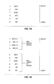
- FIG. 7 a illustrates one embodiment of a client request rankings
- UMA Unified Memory Architecture
- the programs including executable instructions may be executed by one or more programming devices (e.g., a central processing unit (CPU), processor, controller, etc.) in one or more personal computer systems, servers, workstations, etc.
- programming devices e.g., a central processing unit (CPU), processor, controller, etc.
- CPU central processing unit
- controller controller
- personal computer systems servers, workstations, etc.
- MPEG decoder 310 receives and decompresses digital audio and video before it is downloaded into set-top box 300 .
- MPEG decoder 310 implements the MPEG-2 compression standard.
- MPEG related MPEG standards such as the MPEG-I or MPEG-4 standard, may be used.
- non-MPEG standards maybe used.
- Decoder 315 receives composite analog video signals and separates the RGBS (red, green, blue and sync) signals from the video signal. Decoder 315 may be implemented using the National Television System Committee (NTSC) Standard. However, other standards, such as the Phase Alternate Line (PAL), or NTSC/PAL may be used to implement decoder 315 .
- NTSC National Television System Committee
- PAL Phase Alternate Line
- Host interface 450 provides high performance access of memory 325 to CPU 340 .
- host interface 450 includes a cache 455 that services CPU 340 memory transactions.
- Cache 450 may be a small, high speed memory that stores the most recently used instructions or data previously retrieved from memory 325 . Since programs executed by CPU 340 typically use a subset of instructions or data repeatedly, cache 450 is an efficient method of servicing CPU 340 transactions without having to always resort to memory 325 . For example, whenever CPU 340 performs a read operation, it will first check to see if the data or instruction it requests is in cache 450 . If the data is stored in cache 450 , the cache provides the data very quickly to the CPU 340 , without having to access memory 325 .
- FIG. 5 a is a flow diagram of one embodiment of the operation of client interface arbiter 510 .
- client interface arbiter 510 receives a client request.
- process block 808 it is determined whether the recently received request has a higher priority than the other requests. If the recently received request has the highest priority, the MAT signal is transmitted to the client from which the received request originated, process block 810 . At process block 812 , information for the received request is stored at client buffer 520 . Thereafter, control is returned to process block 802 wherein another request is received. However if another request has a higher priority, a MAT signal is transmitted to the higher requesting client, process block 814 . At process block 816 , information for the higher requesting client is stored in an entry of client buffer 520 . Next, control is returned to process block 802 wherein another request is received.
- Client buffer 520 stores entries for each request that has prevailed in arbitration at client interface arbiter 510 .
- Client buffer 520 may store one entry for each type of request at any given time. For example, only one HIF request may be stored in client buffer 520 at a time. Subsequent HIF requests received while an HIF request remains in client buffer 520 is precluded from arbitrating at client interface arbiter 510 .
- the priority scheme implemented in client priority arbiter 530 prevents lower priority clients from being starved from memory 325 services. For example, if a VSC request is competing against an SGFX request at client priority arbiter 530 and VSC 420 is asserting a high priority enable signal, the VSC request prevails provided that DPC 440 is not asserting a high priority enable signal with respect to the SGFX request.
- Each client request for memory 325 access in bank buffer 540 goes through four different stages. As a client request is transmitted to bank buffer 540 the access enters the row activate stage. Consequently, the MEMORY COMMAND field indicates that the pending memory 325 command is a row activate command. The access remains in the row activate stage until after the row activate command has been executed. Subsequently, the access enters the read or write stage, depending upon the type of transaction. The MEMORY COMMAND field indicates that the pending memory command is a read or write command.
- Bank priority arbiter 550 coordinates access to memory 325 by the client requests that are stored in bank buffer 540 .
- Bank priority arbiter 540 selects memory accesses based upon whether the commands stored in Bank A and Bank B are CAS (i.e., read and write) commands or non-CAS (i.e., row activate, precharge and refresh) commands. If a CAS command from one bank is in progress (i.e., client request data transactions), that bank continues to win the arbitration until its access of memory 325 is completed.
- CAS i.e., read and write
- non-CAS i.e., row activate, precharge and refresh
- Bank history and timing unit 560 also maintains cycle counts for time elapsed since the most recent memory command to each bank. The counts maintained are for row activate, read, write, precharge, and refresh accesses to memory 325 . Other time intervals required for correct operation of memory 325 are maintained by counters in bank history and timing unit 560 . These counters may also inhibit a pending command in bank buffer 540 .
- two data fields are stored in memory 325 at any one time.
- Each video field stored in memory 325 contains up to two hundred and forty (240) lines.
- one of the video fields stored in memory 325 corresponds with the top component of the image to be displayed, while the other field corresponds with the bottom component.
- DPC 440 retrieves any complete field that is present in memory 325 at the time encoder 320 indicates it is to transmit a field of data to the display.
- the timing provided by encoder 320 may indicate that DPC 440 is to transmit a top field to the display.
- the top field may not be completely stored in memory 325 at the time it is requested by DPC 440 .
- FIG. 10 is a flow diagram of one embodiment of a display synchronization system used to prevent field inversion.
- fields of video data including the synchronization patterns, are received at memory 325 from VSC 420 .
- the synchronization patterns may be received at memory 325 from a source separate from the video data.
- DPC 440 retrieves the field data and the synchronization pattern data stored in memory 325 .
- the synchronization pattern data is received at comparator 948 .
- synchronization signals are received at field match comparator 948 from encoder 320 via time base unit 942 .
- the synchronization pattern data is compared to the synchronization signals.
Abstract
Description
Claims (9)
Priority Applications (1)
| Application Number | Priority Date | Filing Date | Title |
|---|---|---|---|
| US13/174,456 US8902241B1 (en) | 1999-03-05 | 2011-06-30 | Interactive set-top box having a unified memory architecture |
Applications Claiming Priority (4)
| Application Number | Priority Date | Filing Date | Title |
|---|---|---|---|
| US09/263,454 US6526583B1 (en) | 1999-03-05 | 1999-03-05 | Interactive set-top box having a unified memory architecture |
| US10/288,402 US7688324B1 (en) | 1999-03-05 | 2002-11-04 | Interactive set-top box having a unified memory architecture |
| US12/701,433 US7986326B1 (en) | 1999-03-05 | 2010-02-05 | Interactive set-top box having a unified memory architecture |
| US13/174,456 US8902241B1 (en) | 1999-03-05 | 2011-06-30 | Interactive set-top box having a unified memory architecture |
Related Parent Applications (1)
| Application Number | Title | Priority Date | Filing Date |
|---|---|---|---|
| US12/701,433 Continuation US7986326B1 (en) | 1999-03-05 | 2010-02-05 | Interactive set-top box having a unified memory architecture |
Publications (1)
| Publication Number | Publication Date |
|---|---|
| US8902241B1 true US8902241B1 (en) | 2014-12-02 |
Family
ID=23001849
Family Applications (4)
| Application Number | Title | Priority Date | Filing Date |
|---|---|---|---|
| US09/263,454 Expired - Lifetime US6526583B1 (en) | 1999-03-05 | 1999-03-05 | Interactive set-top box having a unified memory architecture |
| US10/288,402 Expired - Lifetime US7688324B1 (en) | 1999-03-05 | 2002-11-04 | Interactive set-top box having a unified memory architecture |
| US12/701,433 Expired - Fee Related US7986326B1 (en) | 1999-03-05 | 2010-02-05 | Interactive set-top box having a unified memory architecture |
| US13/174,456 Expired - Fee Related US8902241B1 (en) | 1999-03-05 | 2011-06-30 | Interactive set-top box having a unified memory architecture |
Family Applications Before (3)
| Application Number | Title | Priority Date | Filing Date |
|---|---|---|---|
| US09/263,454 Expired - Lifetime US6526583B1 (en) | 1999-03-05 | 1999-03-05 | Interactive set-top box having a unified memory architecture |
| US10/288,402 Expired - Lifetime US7688324B1 (en) | 1999-03-05 | 2002-11-04 | Interactive set-top box having a unified memory architecture |
| US12/701,433 Expired - Fee Related US7986326B1 (en) | 1999-03-05 | 2010-02-05 | Interactive set-top box having a unified memory architecture |
Country Status (1)
| Country | Link |
|---|---|
| US (4) | US6526583B1 (en) |
Families Citing this family (28)
| Publication number | Priority date | Publication date | Assignee | Title |
|---|---|---|---|---|
| US6526583B1 (en) * | 1999-03-05 | 2003-02-25 | Teralogic, Inc. | Interactive set-top box having a unified memory architecture |
| JP3725368B2 (en) * | 1999-05-17 | 2005-12-07 | インターナショナル・ビジネス・マシーンズ・コーポレーション | Image display selection method, computer system, and recording medium |
| US7100000B1 (en) * | 1999-05-28 | 2006-08-29 | International Business Machines Corporation | System and methods for processing audio using multiple speech technologies |
| US8024767B1 (en) * | 1999-09-14 | 2011-09-20 | Ati Technologies Ulc | Method and apparatus for receiving digital video signals |
| US9668011B2 (en) * | 2001-02-05 | 2017-05-30 | Avago Technologies General Ip (Singapore) Pte. Ltd. | Single chip set-top box system |
| EP1109400A1 (en) * | 1999-12-16 | 2001-06-20 | CANAL+ Société Anonyme | Transmission of a command to a receiver or to a decoder |
| WO2002037857A2 (en) * | 2000-10-31 | 2002-05-10 | Koninklijke Philips Electronics N.V. | Method and device for video scene composition including graphic elements |
| US7912220B2 (en) * | 2001-02-05 | 2011-03-22 | Broadcom Corporation | Packetization of non-MPEG stream data in systems using advanced multi-stream POD interface |
| US20020170072A1 (en) * | 2001-05-09 | 2002-11-14 | Lundbald James A. | Systems for receiving and processing digital data carried by satellite transmissions |
| US7530084B2 (en) * | 2002-05-28 | 2009-05-05 | Sony Corporation | Method and apparatus for synchronizing dynamic graphics |
| US20040184523A1 (en) * | 2003-02-25 | 2004-09-23 | Dawson Thomas Patrick | Method and system for providing reduced bandwidth for picture in picture video transmissions |
| US7263587B1 (en) * | 2003-06-27 | 2007-08-28 | Zoran Corporation | Unified memory controller |
| US7307667B1 (en) * | 2003-06-27 | 2007-12-11 | Zoran Corporation | Method and apparatus for an integrated high definition television controller |
| US20050157215A1 (en) * | 2003-09-11 | 2005-07-21 | Echostar Techonologies Corporation | Method and apparatus for detecting an inactive channel selecting resource in a television converter |
| US8087057B2 (en) | 2004-04-28 | 2011-12-27 | Echostar Technologies L.L.C. | Television converter device including an internet protocol interface |
| US8112784B1 (en) | 2004-04-28 | 2012-02-07 | Echostar Corporation | Device comprising multiple channel selectors |
| US7672573B2 (en) * | 2004-05-13 | 2010-03-02 | Sunplus Technology Co., Ltd. | Shared memory architecture and method in an optical storage and recording system |
| US7380036B2 (en) * | 2004-12-10 | 2008-05-27 | Micronas Usa, Inc. | Combined engine for video and graphics processing |
| US9948882B2 (en) * | 2005-08-11 | 2018-04-17 | DISH Technologies L.L.C. | Method and system for toasted video distribution |
| US7930456B1 (en) * | 2006-12-23 | 2011-04-19 | Emc Corporation | Data packet arbitration system |
| US20080262968A1 (en) * | 2007-03-26 | 2008-10-23 | Infosys Technologies Ltd. | Software licensing control via mobile devices |
| US8397010B1 (en) * | 2007-04-16 | 2013-03-12 | Juniper Networks, Inc. | Convenient, flexible, and efficient management of memory space and bandwidth |
| US8861591B2 (en) * | 2007-05-11 | 2014-10-14 | Advanced Micro Devices, Inc. | Software video encoder with GPU acceleration |
| US8233527B2 (en) * | 2007-05-11 | 2012-07-31 | Advanced Micro Devices, Inc. | Software video transcoder with GPU acceleration |
| US8590028B2 (en) | 2007-07-09 | 2013-11-19 | Infosys Limited | Content licensing and conditional access using a mobile device |
| US20090150940A1 (en) * | 2007-12-05 | 2009-06-11 | Echostar Technologies Corporation | Downloading of an interactive application to a broadcast programming receiver |
| JP6022214B2 (en) * | 2012-05-31 | 2016-11-09 | 任天堂株式会社 | Program, information processing method, information processing apparatus, and display system |
| CN108055556B (en) | 2017-11-16 | 2019-09-03 | 北京达佳互联信息技术有限公司 | Data processing method and device |
Citations (25)
| Publication number | Priority date | Publication date | Assignee | Title |
|---|---|---|---|---|
| US4750054A (en) | 1986-10-06 | 1988-06-07 | Eastman Kodak Company | Noise-impervious video timing recovery and automatic skew compensation |
| US5369444A (en) | 1990-06-01 | 1994-11-29 | Thomson Consumer Electronics | Field type matching system |
| US5488389A (en) | 1991-09-25 | 1996-01-30 | Sharp Kabushiki Kaisha | Display device |
| US5553220A (en) | 1993-09-07 | 1996-09-03 | Cirrus Logic, Inc. | Managing audio data using a graphics display controller |
| US5557733A (en) | 1993-04-02 | 1996-09-17 | Vlsi Technology, Inc. | Caching FIFO and method therefor |
| US5598115A (en) | 1993-02-23 | 1997-01-28 | Intergraph Corporation | Comparator cell for use in a content addressable memory |
| US5680591A (en) | 1995-03-28 | 1997-10-21 | Cirrus Logic, Inc. | Method and apparatus for monitoring a row address strobe signal in a graphics controller |
| US5764240A (en) | 1994-08-31 | 1998-06-09 | S3 Incorporated | Method and apparatus for correction of video tearing associated with a video and graphics shared frame buffer, as displayed on a graphics monitor |
| US5790842A (en) | 1996-10-11 | 1998-08-04 | Divicom, Inc. | Processing system with simultaneous utilization of multiple clock signals |
| US5799050A (en) | 1996-04-26 | 1998-08-25 | Nec Corporation | Sync detection circuit and method using variable reference for comparison with mismatch count |
| US5889949A (en) | 1996-10-11 | 1999-03-30 | C-Cube Microsystems | Processing system with memory arbitrating between memory access requests in a set top box |
| US5926647A (en) | 1996-10-11 | 1999-07-20 | Divicom Inc. | Processing system with dynamic alteration of a color look-up table |
| US5936677A (en) | 1997-09-12 | 1999-08-10 | Microsoft Corporation | Microbuffer used in synchronization of image data |
| US6026464A (en) | 1997-06-24 | 2000-02-15 | Cisco Technology, Inc. | Memory control system and method utilizing distributed memory controllers for multibank memory |
| US6037995A (en) | 1996-04-19 | 2000-03-14 | Hitachi, Ltd. | Broadcasting and communication receiver apparatus |
| US6049333A (en) | 1996-09-03 | 2000-04-11 | Time Warner Entertainment Company, L.P. | System and method for providing an event database in a telecasting system |
| US6067098A (en) | 1994-11-16 | 2000-05-23 | Interactive Silicon, Inc. | Video/graphics controller which performs pointer-based display list video refresh operation |
| US6104417A (en) | 1996-09-13 | 2000-08-15 | Silicon Graphics, Inc. | Unified memory computer architecture with dynamic graphics memory allocation |
| US6311268B1 (en) | 1998-11-06 | 2001-10-30 | Acqis Technology, Inc. | Computer module device and method for television use |
| US6356702B1 (en) | 1997-10-30 | 2002-03-12 | Mitsubishi Denki Kabushiki Kaisha | Image display apparatus and special picture reproduction controller |
| US6384723B1 (en) | 1998-11-02 | 2002-05-07 | Pittway Corporation | Digital communication system and method |
| US6424659B2 (en) | 1998-07-17 | 2002-07-23 | Network Equipment Technologies, Inc. | Multi-layer switching apparatus and method |
| US6457114B1 (en) | 1997-04-30 | 2002-09-24 | Sony Corporation | Asynchronous memory interface for a video processor with a 2N sized buffer and N+1 wide bit gray coded counters |
| US6526583B1 (en) | 1999-03-05 | 2003-02-25 | Teralogic, Inc. | Interactive set-top box having a unified memory architecture |
| US7095783B1 (en) | 1992-06-30 | 2006-08-22 | Discovision Associates | Multistandard video decoder and decompression system for processing encoded bit streams including start codes and methods relating thereto |
-
1999
- 1999-03-05 US US09/263,454 patent/US6526583B1/en not_active Expired - Lifetime
-
2002
- 2002-11-04 US US10/288,402 patent/US7688324B1/en not_active Expired - Lifetime
-
2010
- 2010-02-05 US US12/701,433 patent/US7986326B1/en not_active Expired - Fee Related
-
2011
- 2011-06-30 US US13/174,456 patent/US8902241B1/en not_active Expired - Fee Related
Patent Citations (27)
| Publication number | Priority date | Publication date | Assignee | Title |
|---|---|---|---|---|
| US4750054A (en) | 1986-10-06 | 1988-06-07 | Eastman Kodak Company | Noise-impervious video timing recovery and automatic skew compensation |
| US5369444A (en) | 1990-06-01 | 1994-11-29 | Thomson Consumer Electronics | Field type matching system |
| US5488389A (en) | 1991-09-25 | 1996-01-30 | Sharp Kabushiki Kaisha | Display device |
| US7095783B1 (en) | 1992-06-30 | 2006-08-22 | Discovision Associates | Multistandard video decoder and decompression system for processing encoded bit streams including start codes and methods relating thereto |
| US5598115A (en) | 1993-02-23 | 1997-01-28 | Intergraph Corporation | Comparator cell for use in a content addressable memory |
| US5557733A (en) | 1993-04-02 | 1996-09-17 | Vlsi Technology, Inc. | Caching FIFO and method therefor |
| US5553220A (en) | 1993-09-07 | 1996-09-03 | Cirrus Logic, Inc. | Managing audio data using a graphics display controller |
| US5764240A (en) | 1994-08-31 | 1998-06-09 | S3 Incorporated | Method and apparatus for correction of video tearing associated with a video and graphics shared frame buffer, as displayed on a graphics monitor |
| US6067098A (en) | 1994-11-16 | 2000-05-23 | Interactive Silicon, Inc. | Video/graphics controller which performs pointer-based display list video refresh operation |
| US5680591A (en) | 1995-03-28 | 1997-10-21 | Cirrus Logic, Inc. | Method and apparatus for monitoring a row address strobe signal in a graphics controller |
| US6037995A (en) | 1996-04-19 | 2000-03-14 | Hitachi, Ltd. | Broadcasting and communication receiver apparatus |
| US5799050A (en) | 1996-04-26 | 1998-08-25 | Nec Corporation | Sync detection circuit and method using variable reference for comparison with mismatch count |
| US6049333A (en) | 1996-09-03 | 2000-04-11 | Time Warner Entertainment Company, L.P. | System and method for providing an event database in a telecasting system |
| US6104417A (en) | 1996-09-13 | 2000-08-15 | Silicon Graphics, Inc. | Unified memory computer architecture with dynamic graphics memory allocation |
| US5926647A (en) | 1996-10-11 | 1999-07-20 | Divicom Inc. | Processing system with dynamic alteration of a color look-up table |
| US5889949A (en) | 1996-10-11 | 1999-03-30 | C-Cube Microsystems | Processing system with memory arbitrating between memory access requests in a set top box |
| US5790842A (en) | 1996-10-11 | 1998-08-04 | Divicom, Inc. | Processing system with simultaneous utilization of multiple clock signals |
| US6457114B1 (en) | 1997-04-30 | 2002-09-24 | Sony Corporation | Asynchronous memory interface for a video processor with a 2N sized buffer and N+1 wide bit gray coded counters |
| US6026464A (en) | 1997-06-24 | 2000-02-15 | Cisco Technology, Inc. | Memory control system and method utilizing distributed memory controllers for multibank memory |
| US5936677A (en) | 1997-09-12 | 1999-08-10 | Microsoft Corporation | Microbuffer used in synchronization of image data |
| US6356702B1 (en) | 1997-10-30 | 2002-03-12 | Mitsubishi Denki Kabushiki Kaisha | Image display apparatus and special picture reproduction controller |
| US6424659B2 (en) | 1998-07-17 | 2002-07-23 | Network Equipment Technologies, Inc. | Multi-layer switching apparatus and method |
| US6384723B1 (en) | 1998-11-02 | 2002-05-07 | Pittway Corporation | Digital communication system and method |
| US6311268B1 (en) | 1998-11-06 | 2001-10-30 | Acqis Technology, Inc. | Computer module device and method for television use |
| US6526583B1 (en) | 1999-03-05 | 2003-02-25 | Teralogic, Inc. | Interactive set-top box having a unified memory architecture |
| US7688324B1 (en) | 1999-03-05 | 2010-03-30 | Zoran Corporation | Interactive set-top box having a unified memory architecture |
| US7986326B1 (en) | 1999-03-05 | 2011-07-26 | Zoran Corporation | Interactive set-top box having a unified memory architecture |
Also Published As
| Publication number | Publication date |
|---|---|
| US7986326B1 (en) | 2011-07-26 |
| US6526583B1 (en) | 2003-02-25 |
| US7688324B1 (en) | 2010-03-30 |
Similar Documents
| Publication | Publication Date | Title |
|---|---|---|
| US8902241B1 (en) | Interactive set-top box having a unified memory architecture | |
| US8314808B2 (en) | Electronic system and method for selectively allowing access to a shared memory | |
| US7773676B2 (en) | Video decoding system with external memory rearranging on a field or frames basis | |
| KR100262453B1 (en) | Method and apparatus for processing video data | |
| US6091431A (en) | Method and apparatus for improving processor to graphics device local memory performance | |
| US6335950B1 (en) | Motion estimation engine | |
| TW201116065A (en) | Memory address mapping method and memory address mapping circuit | |
| JPH10512968A (en) | More efficient memory bandwidth | |
| JP3141772B2 (en) | MPEG decoder and decoding method thereof | |
| US6342895B1 (en) | Apparatus and method for memory allocation | |
| US6717989B1 (en) | Video decoding apparatus and method for a shared display memory system | |
| US20040066450A1 (en) | Apparatus and method for generating an interleaved stereo image | |
| US6919902B2 (en) | Method and apparatus for fetching pixel data from memory | |
| US5883679A (en) | Scanning scheme for images stored in dynamic random access memory | |
| US5748968A (en) | Requesting device capable of canceling its memory access requests upon detecting other specific requesting devices simultaneously asserting access requests | |
| EP0772159B1 (en) | Memory sharing in a MPEG decoder | |
| US20130120420A1 (en) | Method and system for efficiently organizing data in memory | |
| US7512752B2 (en) | Systems, methods, and apparatus for pixel fetch request interface | |
| CN117851293A (en) | Address translation module, display controller, processing system, electronic component, electronic device, and page table prefetching method | |
| US8265169B2 (en) | Video block memory read request translation and tagging | |
| US8035740B2 (en) | Image processing apparatus and method |
Legal Events
| Date | Code | Title | Description |
|---|---|---|---|
| STCF | Information on status: patent grant |
Free format text: PATENTED CASE |
|
| AS | Assignment |
Owner name: TERALOGIC, INC., CALIFORNIA Free format text: ASSIGNMENT OF ASSIGNORS INTEREST;ASSIGNORS:AULD, DAVID R.;HOLMER, BRUCE K.;HUANG, HONG-JYEH JASON;AND OTHERS;SIGNING DATES FROM 19990506 TO 19990513;REEL/FRAME:038175/0531 Owner name: TERALOGIC GROUP, INC., CALIFORNIA Free format text: MERGER AND CHANGE OF NAME;ASSIGNORS:OPTIC ACQUISITION CORP.;TERALOGIC, INC.;REEL/FRAME:038175/0568 Effective date: 20021025 Owner name: CSR TECHNOLOGY INC., CALIFORNIA Free format text: ASSIGNMENT OF ASSIGNORS INTEREST;ASSIGNOR:ZORAN CORPORATION;REEL/FRAME:038175/0770 Effective date: 20150915 Owner name: CSR TECHNOLOGY INC., CALIFORNIA Free format text: ASSIGNMENT OF ASSIGNORS INTEREST;ASSIGNOR:ZORAN CORPORATION;REEL/FRAME:038175/0687 Effective date: 20120101 |
|
| AS | Assignment |
Owner name: ZORAN CORPORATION, CALIFORNIA Free format text: NUNC PRO TUNC ASSIGNMENT;ASSIGNOR:TERALOGIC INC.;REEL/FRAME:038217/0206 Effective date: 20041106 |
|
| AS | Assignment |
Owner name: ZORAN CORPORATION, CALIFORNIA Free format text: ASSIGNMENT OF ASSIGNORS INTEREST;ASSIGNOR:TERALOGIC INC.;REEL/FRAME:038936/0563 Effective date: 20041106 |
|
| AS | Assignment |
Owner name: ZORAN CORPORATION, CALIFORNIA Free format text: CORRECTIVE ASSIGNMENT TO CORRECT THE NAME OF THE ASSIGNOR PREVIOUSLY RECORDED ON REEL 038936 FRAME 0563. ASSIGNOR(S) HEREBY CONFIRMS THE ASSIGNMENT FROM TERALOGIC GROUP, INC. TO ZORAN CORPORATION;ASSIGNOR:TERALOGIC GROUP, INC.;REEL/FRAME:039092/0482 Effective date: 20041106 |
|
| MAFP | Maintenance fee payment |
Free format text: PAYMENT OF MAINTENANCE FEE, 4TH YEAR, LARGE ENTITY (ORIGINAL EVENT CODE: M1551) Year of fee payment: 4 |
|
| FEPP | Fee payment procedure |
Free format text: MAINTENANCE FEE REMINDER MAILED (ORIGINAL EVENT CODE: REM.); ENTITY STATUS OF PATENT OWNER: LARGE ENTITY |
|
| LAPS | Lapse for failure to pay maintenance fees |
Free format text: PATENT EXPIRED FOR FAILURE TO PAY MAINTENANCE FEES (ORIGINAL EVENT CODE: EXP.); ENTITY STATUS OF PATENT OWNER: LARGE ENTITY |
|
| STCH | Information on status: patent discontinuation |
Free format text: PATENT EXPIRED DUE TO NONPAYMENT OF MAINTENANCE FEES UNDER 37 CFR 1.362 |
|
| FP | Lapsed due to failure to pay maintenance fee |
Effective date: 20221202 |