US8937010B2 - Information encoding using wirebonds - Google Patents
Information encoding using wirebonds Download PDFInfo
- Publication number
- US8937010B2 US8937010B2 US13/779,036 US201313779036A US8937010B2 US 8937010 B2 US8937010 B2 US 8937010B2 US 201313779036 A US201313779036 A US 201313779036A US 8937010 B2 US8937010 B2 US 8937010B2
- Authority
- US
- United States
- Prior art keywords
- chip
- integrated circuit
- pads
- chip pads
- information
- Prior art date
- Legal status (The legal status is an assumption and is not a legal conclusion. Google has not performed a legal analysis and makes no representation as to the accuracy of the status listed.)
- Expired - Fee Related
Links
Images


Classifications
-
- G—PHYSICS
- G06—COMPUTING; CALCULATING OR COUNTING
- G06F—ELECTRIC DIGITAL DATA PROCESSING
- G06F21/00—Security arrangements for protecting computers, components thereof, programs or data against unauthorised activity
- G06F21/70—Protecting specific internal or peripheral components, in which the protection of a component leads to protection of the entire computer
- G06F21/71—Protecting specific internal or peripheral components, in which the protection of a component leads to protection of the entire computer to assure secure computing or processing of information
- G06F21/73—Protecting specific internal or peripheral components, in which the protection of a component leads to protection of the entire computer to assure secure computing or processing of information by creating or determining hardware identification, e.g. serial numbers
-
- H—ELECTRICITY
- H01—ELECTRIC ELEMENTS
- H01L—SEMICONDUCTOR DEVICES NOT COVERED BY CLASS H10
- H01L24/00—Arrangements for connecting or disconnecting semiconductor or solid-state bodies; Methods or apparatus related thereto
- H01L24/80—Methods for connecting semiconductor or other solid state bodies using means for bonding being attached to, or being formed on, the surface to be connected
- H01L24/81—Methods for connecting semiconductor or other solid state bodies using means for bonding being attached to, or being formed on, the surface to be connected using a bump connector
-
- H—ELECTRICITY
- H01—ELECTRIC ELEMENTS
- H01L—SEMICONDUCTOR DEVICES NOT COVERED BY CLASS H10
- H01L23/00—Details of semiconductor or other solid state devices
- H01L23/48—Arrangements for conducting electric current to or from the solid state body in operation, e.g. leads, terminal arrangements ; Selection of materials therefor
- H01L23/488—Arrangements for conducting electric current to or from the solid state body in operation, e.g. leads, terminal arrangements ; Selection of materials therefor consisting of soldered or bonded constructions
-
- H—ELECTRICITY
- H01—ELECTRIC ELEMENTS
- H01L—SEMICONDUCTOR DEVICES NOT COVERED BY CLASS H10
- H01L23/00—Details of semiconductor or other solid state devices
- H01L23/544—Marks applied to semiconductor devices or parts, e.g. registration marks, alignment structures, wafer maps
-
- H—ELECTRICITY
- H01—ELECTRIC ELEMENTS
- H01L—SEMICONDUCTOR DEVICES NOT COVERED BY CLASS H10
- H01L24/00—Arrangements for connecting or disconnecting semiconductor or solid-state bodies; Methods or apparatus related thereto
- H01L24/01—Means for bonding being attached to, or being formed on, the surface to be connected, e.g. chip-to-package, die-attach, "first-level" interconnects; Manufacturing methods related thereto
- H01L24/42—Wire connectors; Manufacturing methods related thereto
- H01L24/47—Structure, shape, material or disposition of the wire connectors after the connecting process
- H01L24/48—Structure, shape, material or disposition of the wire connectors after the connecting process of an individual wire connector
-
- H—ELECTRICITY
- H01—ELECTRIC ELEMENTS
- H01L—SEMICONDUCTOR DEVICES NOT COVERED BY CLASS H10
- H01L24/00—Arrangements for connecting or disconnecting semiconductor or solid-state bodies; Methods or apparatus related thereto
- H01L24/01—Means for bonding being attached to, or being formed on, the surface to be connected, e.g. chip-to-package, die-attach, "first-level" interconnects; Manufacturing methods related thereto
- H01L24/42—Wire connectors; Manufacturing methods related thereto
- H01L24/47—Structure, shape, material or disposition of the wire connectors after the connecting process
- H01L24/49—Structure, shape, material or disposition of the wire connectors after the connecting process of a plurality of wire connectors
-
- H—ELECTRICITY
- H01—ELECTRIC ELEMENTS
- H01L—SEMICONDUCTOR DEVICES NOT COVERED BY CLASS H10
- H01L24/00—Arrangements for connecting or disconnecting semiconductor or solid-state bodies; Methods or apparatus related thereto
- H01L24/80—Methods for connecting semiconductor or other solid state bodies using means for bonding being attached to, or being formed on, the surface to be connected
- H01L24/85—Methods for connecting semiconductor or other solid state bodies using means for bonding being attached to, or being formed on, the surface to be connected using a wire connector
-
- H—ELECTRICITY
- H01—ELECTRIC ELEMENTS
- H01L—SEMICONDUCTOR DEVICES NOT COVERED BY CLASS H10
- H01L2223/00—Details relating to semiconductor or other solid state devices covered by the group H01L23/00
- H01L2223/544—Marks applied to semiconductor devices or parts
- H01L2223/54433—Marks applied to semiconductor devices or parts containing identification or tracking information
-
- H—ELECTRICITY
- H01—ELECTRIC ELEMENTS
- H01L—SEMICONDUCTOR DEVICES NOT COVERED BY CLASS H10
- H01L2223/00—Details relating to semiconductor or other solid state devices covered by the group H01L23/00
- H01L2223/544—Marks applied to semiconductor devices or parts
- H01L2223/54473—Marks applied to semiconductor devices or parts for use after dicing
- H01L2223/54486—Located on package parts, e.g. encapsulation, leads, package substrate
-
- H—ELECTRICITY
- H01—ELECTRIC ELEMENTS
- H01L—SEMICONDUCTOR DEVICES NOT COVERED BY CLASS H10
- H01L2224/00—Indexing scheme for arrangements for connecting or disconnecting semiconductor or solid-state bodies and methods related thereto as covered by H01L24/00
- H01L2224/01—Means for bonding being attached to, or being formed on, the surface to be connected, e.g. chip-to-package, die-attach, "first-level" interconnects; Manufacturing methods related thereto
- H01L2224/02—Bonding areas; Manufacturing methods related thereto
- H01L2224/04—Structure, shape, material or disposition of the bonding areas prior to the connecting process
- H01L2224/04042—Bonding areas specifically adapted for wire connectors, e.g. wirebond pads
-
- H—ELECTRICITY
- H01—ELECTRIC ELEMENTS
- H01L—SEMICONDUCTOR DEVICES NOT COVERED BY CLASS H10
- H01L2224/00—Indexing scheme for arrangements for connecting or disconnecting semiconductor or solid-state bodies and methods related thereto as covered by H01L24/00
- H01L2224/01—Means for bonding being attached to, or being formed on, the surface to be connected, e.g. chip-to-package, die-attach, "first-level" interconnects; Manufacturing methods related thereto
- H01L2224/02—Bonding areas; Manufacturing methods related thereto
- H01L2224/04—Structure, shape, material or disposition of the bonding areas prior to the connecting process
- H01L2224/05—Structure, shape, material or disposition of the bonding areas prior to the connecting process of an individual bonding area
- H01L2224/0554—External layer
- H01L2224/0555—Shape
- H01L2224/05552—Shape in top view
- H01L2224/05553—Shape in top view being rectangular
-
- H—ELECTRICITY
- H01—ELECTRIC ELEMENTS
- H01L—SEMICONDUCTOR DEVICES NOT COVERED BY CLASS H10
- H01L2224/00—Indexing scheme for arrangements for connecting or disconnecting semiconductor or solid-state bodies and methods related thereto as covered by H01L24/00
- H01L2224/01—Means for bonding being attached to, or being formed on, the surface to be connected, e.g. chip-to-package, die-attach, "first-level" interconnects; Manufacturing methods related thereto
- H01L2224/02—Bonding areas; Manufacturing methods related thereto
- H01L2224/04—Structure, shape, material or disposition of the bonding areas prior to the connecting process
- H01L2224/06—Structure, shape, material or disposition of the bonding areas prior to the connecting process of a plurality of bonding areas
- H01L2224/061—Disposition
- H01L2224/0612—Layout
-
- H—ELECTRICITY
- H01—ELECTRIC ELEMENTS
- H01L—SEMICONDUCTOR DEVICES NOT COVERED BY CLASS H10
- H01L2224/00—Indexing scheme for arrangements for connecting or disconnecting semiconductor or solid-state bodies and methods related thereto as covered by H01L24/00
- H01L2224/01—Means for bonding being attached to, or being formed on, the surface to be connected, e.g. chip-to-package, die-attach, "first-level" interconnects; Manufacturing methods related thereto
- H01L2224/42—Wire connectors; Manufacturing methods related thereto
- H01L2224/44—Structure, shape, material or disposition of the wire connectors prior to the connecting process
- H01L2224/45—Structure, shape, material or disposition of the wire connectors prior to the connecting process of an individual wire connector
- H01L2224/45001—Core members of the connector
- H01L2224/4501—Shape
- H01L2224/45012—Cross-sectional shape
- H01L2224/45015—Cross-sectional shape being circular
-
- H—ELECTRICITY
- H01—ELECTRIC ELEMENTS
- H01L—SEMICONDUCTOR DEVICES NOT COVERED BY CLASS H10
- H01L2224/00—Indexing scheme for arrangements for connecting or disconnecting semiconductor or solid-state bodies and methods related thereto as covered by H01L24/00
- H01L2224/01—Means for bonding being attached to, or being formed on, the surface to be connected, e.g. chip-to-package, die-attach, "first-level" interconnects; Manufacturing methods related thereto
- H01L2224/42—Wire connectors; Manufacturing methods related thereto
- H01L2224/44—Structure, shape, material or disposition of the wire connectors prior to the connecting process
- H01L2224/45—Structure, shape, material or disposition of the wire connectors prior to the connecting process of an individual wire connector
- H01L2224/45001—Core members of the connector
- H01L2224/45099—Material
- H01L2224/451—Material with a principal constituent of the material being a metal or a metalloid, e.g. boron (B), silicon (Si), germanium (Ge), arsenic (As), antimony (Sb), tellurium (Te) and polonium (Po), and alloys thereof
- H01L2224/45138—Material with a principal constituent of the material being a metal or a metalloid, e.g. boron (B), silicon (Si), germanium (Ge), arsenic (As), antimony (Sb), tellurium (Te) and polonium (Po), and alloys thereof the principal constituent melting at a temperature of greater than or equal to 950°C and less than 1550°C
- H01L2224/45144—Gold (Au) as principal constituent
-
- H—ELECTRICITY
- H01—ELECTRIC ELEMENTS
- H01L—SEMICONDUCTOR DEVICES NOT COVERED BY CLASS H10
- H01L2224/00—Indexing scheme for arrangements for connecting or disconnecting semiconductor or solid-state bodies and methods related thereto as covered by H01L24/00
- H01L2224/01—Means for bonding being attached to, or being formed on, the surface to be connected, e.g. chip-to-package, die-attach, "first-level" interconnects; Manufacturing methods related thereto
- H01L2224/42—Wire connectors; Manufacturing methods related thereto
- H01L2224/47—Structure, shape, material or disposition of the wire connectors after the connecting process
- H01L2224/48—Structure, shape, material or disposition of the wire connectors after the connecting process of an individual wire connector
- H01L2224/481—Disposition
- H01L2224/48151—Connecting between a semiconductor or solid-state body and an item not being a semiconductor or solid-state body, e.g. chip-to-substrate, chip-to-passive
- H01L2224/48221—Connecting between a semiconductor or solid-state body and an item not being a semiconductor or solid-state body, e.g. chip-to-substrate, chip-to-passive the body and the item being stacked
- H01L2224/48245—Connecting between a semiconductor or solid-state body and an item not being a semiconductor or solid-state body, e.g. chip-to-substrate, chip-to-passive the body and the item being stacked the item being metallic
- H01L2224/48247—Connecting between a semiconductor or solid-state body and an item not being a semiconductor or solid-state body, e.g. chip-to-substrate, chip-to-passive the body and the item being stacked the item being metallic connecting the wire to a bond pad of the item
-
- H—ELECTRICITY
- H01—ELECTRIC ELEMENTS
- H01L—SEMICONDUCTOR DEVICES NOT COVERED BY CLASS H10
- H01L2224/00—Indexing scheme for arrangements for connecting or disconnecting semiconductor or solid-state bodies and methods related thereto as covered by H01L24/00
- H01L2224/01—Means for bonding being attached to, or being formed on, the surface to be connected, e.g. chip-to-package, die-attach, "first-level" interconnects; Manufacturing methods related thereto
- H01L2224/42—Wire connectors; Manufacturing methods related thereto
- H01L2224/47—Structure, shape, material or disposition of the wire connectors after the connecting process
- H01L2224/48—Structure, shape, material or disposition of the wire connectors after the connecting process of an individual wire connector
- H01L2224/484—Connecting portions
- H01L2224/48463—Connecting portions the connecting portion on the bonding area of the semiconductor or solid-state body being a ball bond
- H01L2224/48465—Connecting portions the connecting portion on the bonding area of the semiconductor or solid-state body being a ball bond the other connecting portion not on the bonding area being a wedge bond, i.e. ball-to-wedge, regular stitch
-
- H—ELECTRICITY
- H01—ELECTRIC ELEMENTS
- H01L—SEMICONDUCTOR DEVICES NOT COVERED BY CLASS H10
- H01L2224/00—Indexing scheme for arrangements for connecting or disconnecting semiconductor or solid-state bodies and methods related thereto as covered by H01L24/00
- H01L2224/01—Means for bonding being attached to, or being formed on, the surface to be connected, e.g. chip-to-package, die-attach, "first-level" interconnects; Manufacturing methods related thereto
- H01L2224/42—Wire connectors; Manufacturing methods related thereto
- H01L2224/47—Structure, shape, material or disposition of the wire connectors after the connecting process
- H01L2224/49—Structure, shape, material or disposition of the wire connectors after the connecting process of a plurality of wire connectors
- H01L2224/4901—Structure
- H01L2224/4903—Connectors having different sizes, e.g. different diameters
-
- H—ELECTRICITY
- H01—ELECTRIC ELEMENTS
- H01L—SEMICONDUCTOR DEVICES NOT COVERED BY CLASS H10
- H01L2224/00—Indexing scheme for arrangements for connecting or disconnecting semiconductor or solid-state bodies and methods related thereto as covered by H01L24/00
- H01L2224/01—Means for bonding being attached to, or being formed on, the surface to be connected, e.g. chip-to-package, die-attach, "first-level" interconnects; Manufacturing methods related thereto
- H01L2224/42—Wire connectors; Manufacturing methods related thereto
- H01L2224/47—Structure, shape, material or disposition of the wire connectors after the connecting process
- H01L2224/49—Structure, shape, material or disposition of the wire connectors after the connecting process of a plurality of wire connectors
- H01L2224/491—Disposition
- H01L2224/4912—Layout
- H01L2224/49175—Parallel arrangements
-
- H—ELECTRICITY
- H01—ELECTRIC ELEMENTS
- H01L—SEMICONDUCTOR DEVICES NOT COVERED BY CLASS H10
- H01L2224/00—Indexing scheme for arrangements for connecting or disconnecting semiconductor or solid-state bodies and methods related thereto as covered by H01L24/00
- H01L2224/01—Means for bonding being attached to, or being formed on, the surface to be connected, e.g. chip-to-package, die-attach, "first-level" interconnects; Manufacturing methods related thereto
- H01L2224/42—Wire connectors; Manufacturing methods related thereto
- H01L2224/47—Structure, shape, material or disposition of the wire connectors after the connecting process
- H01L2224/49—Structure, shape, material or disposition of the wire connectors after the connecting process of a plurality of wire connectors
- H01L2224/494—Connecting portions
- H01L2224/4943—Connecting portions the connecting portions being staggered
- H01L2224/49431—Connecting portions the connecting portions being staggered on the semiconductor or solid-state body
-
- H—ELECTRICITY
- H01—ELECTRIC ELEMENTS
- H01L—SEMICONDUCTOR DEVICES NOT COVERED BY CLASS H10
- H01L2224/00—Indexing scheme for arrangements for connecting or disconnecting semiconductor or solid-state bodies and methods related thereto as covered by H01L24/00
- H01L2224/01—Means for bonding being attached to, or being formed on, the surface to be connected, e.g. chip-to-package, die-attach, "first-level" interconnects; Manufacturing methods related thereto
- H01L2224/42—Wire connectors; Manufacturing methods related thereto
- H01L2224/47—Structure, shape, material or disposition of the wire connectors after the connecting process
- H01L2224/49—Structure, shape, material or disposition of the wire connectors after the connecting process of a plurality of wire connectors
- H01L2224/494—Connecting portions
- H01L2224/4943—Connecting portions the connecting portions being staggered
- H01L2224/49433—Connecting portions the connecting portions being staggered outside the semiconductor or solid-state body
-
- H—ELECTRICITY
- H01—ELECTRIC ELEMENTS
- H01L—SEMICONDUCTOR DEVICES NOT COVERED BY CLASS H10
- H01L2224/00—Indexing scheme for arrangements for connecting or disconnecting semiconductor or solid-state bodies and methods related thereto as covered by H01L24/00
- H01L2224/80—Methods for connecting semiconductor or other solid state bodies using means for bonding being attached to, or being formed on, the surface to be connected
- H01L2224/85—Methods for connecting semiconductor or other solid state bodies using means for bonding being attached to, or being formed on, the surface to be connected using a wire connector
- H01L2224/852—Applying energy for connecting
- H01L2224/85201—Compression bonding
- H01L2224/85203—Thermocompression bonding
-
- H—ELECTRICITY
- H01—ELECTRIC ELEMENTS
- H01L—SEMICONDUCTOR DEVICES NOT COVERED BY CLASS H10
- H01L2224/00—Indexing scheme for arrangements for connecting or disconnecting semiconductor or solid-state bodies and methods related thereto as covered by H01L24/00
- H01L2224/80—Methods for connecting semiconductor or other solid state bodies using means for bonding being attached to, or being formed on, the surface to be connected
- H01L2224/85—Methods for connecting semiconductor or other solid state bodies using means for bonding being attached to, or being formed on, the surface to be connected using a wire connector
- H01L2224/852—Applying energy for connecting
- H01L2224/85201—Compression bonding
- H01L2224/85205—Ultrasonic bonding
-
- H—ELECTRICITY
- H01—ELECTRIC ELEMENTS
- H01L—SEMICONDUCTOR DEVICES NOT COVERED BY CLASS H10
- H01L24/00—Arrangements for connecting or disconnecting semiconductor or solid-state bodies; Methods or apparatus related thereto
- H01L24/01—Means for bonding being attached to, or being formed on, the surface to be connected, e.g. chip-to-package, die-attach, "first-level" interconnects; Manufacturing methods related thereto
- H01L24/02—Bonding areas ; Manufacturing methods related thereto
- H01L24/04—Structure, shape, material or disposition of the bonding areas prior to the connecting process
- H01L24/05—Structure, shape, material or disposition of the bonding areas prior to the connecting process of an individual bonding area
-
- H—ELECTRICITY
- H01—ELECTRIC ELEMENTS
- H01L—SEMICONDUCTOR DEVICES NOT COVERED BY CLASS H10
- H01L24/00—Arrangements for connecting or disconnecting semiconductor or solid-state bodies; Methods or apparatus related thereto
- H01L24/01—Means for bonding being attached to, or being formed on, the surface to be connected, e.g. chip-to-package, die-attach, "first-level" interconnects; Manufacturing methods related thereto
- H01L24/02—Bonding areas ; Manufacturing methods related thereto
- H01L24/04—Structure, shape, material or disposition of the bonding areas prior to the connecting process
- H01L24/06—Structure, shape, material or disposition of the bonding areas prior to the connecting process of a plurality of bonding areas
-
- H—ELECTRICITY
- H01—ELECTRIC ELEMENTS
- H01L—SEMICONDUCTOR DEVICES NOT COVERED BY CLASS H10
- H01L24/00—Arrangements for connecting or disconnecting semiconductor or solid-state bodies; Methods or apparatus related thereto
- H01L24/01—Means for bonding being attached to, or being formed on, the surface to be connected, e.g. chip-to-package, die-attach, "first-level" interconnects; Manufacturing methods related thereto
- H01L24/42—Wire connectors; Manufacturing methods related thereto
- H01L24/44—Structure, shape, material or disposition of the wire connectors prior to the connecting process
- H01L24/45—Structure, shape, material or disposition of the wire connectors prior to the connecting process of an individual wire connector
-
- H—ELECTRICITY
- H01—ELECTRIC ELEMENTS
- H01L—SEMICONDUCTOR DEVICES NOT COVERED BY CLASS H10
- H01L2924/00—Indexing scheme for arrangements or methods for connecting or disconnecting semiconductor or solid-state bodies as covered by H01L24/00
- H01L2924/0001—Technical content checked by a classifier
- H01L2924/00014—Technical content checked by a classifier the subject-matter covered by the group, the symbol of which is combined with the symbol of this group, being disclosed without further technical details
-
- H—ELECTRICITY
- H01—ELECTRIC ELEMENTS
- H01L—SEMICONDUCTOR DEVICES NOT COVERED BY CLASS H10
- H01L2924/00—Indexing scheme for arrangements or methods for connecting or disconnecting semiconductor or solid-state bodies as covered by H01L24/00
- H01L2924/15—Details of package parts other than the semiconductor or other solid state devices to be connected
- H01L2924/181—Encapsulation
Definitions
- the present invention relates to the field of integrated circuits chip; more specifically, it relates to on-chip information encoding.
- Modern integrated circuit chips include electronic chip identification (ECID) circuits that electronically encode a unique integrated circuit (IC) chip identification, or other IC chip related data that can be read out after manufacturing is complete.
- ECID electronic chip identification
- IC integrated circuit
- these ECID circuits must be part of the integrated circuit design and require special equipment to encode the information on the IC chip.
- Many smaller companies lack the means to implement ECID and many IC designs lack the space or cannot support the cost of ECID. Accordingly, there exists a need in the art to mitigate the deficiencies and limitations described hereinabove.
- a first aspect of the present invention is a method of encoding information on an integrated circuit chip, comprising: selecting a set of chip pads of the integrated circuit chip for encoding the information; encoding the information during a wirebonding process, the wirebonding process comprising forming ball bonds on chip pads of the integrated circuit chip and wedge bonds on leadframe fingers adjacent to one or more edges of the integrated circuit chip, the ball bonds and the wedge bonds connected by respective and integral wires; and wherein the information is encoded by varying one or more wirebonding parameters on each chip pad of the set of chip pads, the wirebonding parameters selected from the group consisting of the location of a ball bond on a chip pad, the diameter of a ball bond on a chip pad, both the location and diameter of a ball bond on a chip pad, the location of a wedge bond on a leadframe finger and combinations thereof.
- a second aspect of the present invention is a structure encoding information on an integrated circuit chip, comprising: a set of chip pads on the integrated circuit chip and corresponding leadframe fingers adjacent to a perimeter of the integrated circuit chip; ball bonds on the chip pads of the integrated circuit chip and wedge bonds on the leadframe fingers, the ball bonds and the wedge bonds connected by respective and integral wires; and wherein said information is encoded by locations of ball bonds on selected chip pads, diameters of a ball bonds on selected chip pads, both the locations and diameters of ball bonds on selected chip pads, locations of wedge bonds on selected leadframe fingers and combinations thereof.
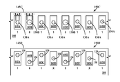
- FIG. 1 a top view of an exemplary integrated circuit chip illustrating interconnection of the chip to a leadframe using wirebonds
- FIG. 3 illustrates a method for binary encoding of information on an integrated circuit chip using wirebonds according to embodiments of the present invention
- FIG. 4 illustrates in more detail, the principle of binary data encoding according to embodiments of the present invention
- FIG. 5 illustrates non-position dependent binary data encoding of information using wirebonds according to embodiments of the present invention
- FIG. 6 illustrates a method for tertiary encoding of information on an integrated circuit chip using wirebonds according to embodiments of the present invention
- FIG. 7 illustrates in more detail, the principle of tertiary data encoding according to embodiments of the present invention
- FIG. 8 illustrates a first method for N-based encoding of information on an integrated circuit chip using wirebonds according to embodiments of the present invention
- FIG. 9 illustrates a second method for N-based encoding of information on an integrated circuit chip using wirebonds according to embodiments of the present invention.
- FIG. 11 is a side view of a wirebonded integrated circuit module
- FIG. 13 illustrates the principle of binary data encoding using the wedge bond according to embodiments of the present invention.
- FIG. 14 is a flow diagram of the method of encoding information using wirebonds according to embodiments of the present invention.
- the embodiments of the present invention encode integrated circuit specific information based on the position of the ball bond of wirebonds, the size of the ball bond of wirebonds or a combination of the position and size of ball bonds of wirebonds on chip pads of integrated circuit chips.
- the embodiments of the present invention may be practiced using the position of the wedge bond of wirebonds on leadframe fingers of integrated circuit modules.
- the position of the ball bond of wirebonds, the size of the ball bond of wirebonds or a combination of the position and size of ball bonds of wirebonds that are used to encode information are placed on chip pads selected for encoding information so that other ball bonds on non-selected chip pads do not encode information even if they mimic the encoded structures as to position of the ball bond or size of the ball bond on the non-selected chip pads.
- FIG. 1 a top view of an exemplary integrated circuit chip illustrating interconnection of the chip to a leadframe using wirebonds.
- an integrated circuit chip includes a plurality of chip pads 105 arranged around the perimeter of integrated circuit chip 100 .
- a plurality of leadframe fingers 115 are arranged opposite chip pads 105 , but do not touch integrated circuit chip 100 .
- Chip pads 105 are connected to respective leadframe fingers 115 by electrically conductive wirebonds 120 .
- Chip pads 105 are electrically connected to semiconductor devices (e.g., field effect transistors (FETs)) of integrated circuit chip 100 .
- Chip pads 105 may carry signals in and out of integrated circuit chip 100 or may supply power to integrated circuit chip 100 .
- FETs field effect transistors
- While four rows of chip pads adjacent to respective edges of integrated circuit chip 100 are illustrated, there may be less than four rows. For example, there may be only two rows arranged on opposite sides of integrated circuit chip 100 (see FIG. 12 ). Further, while a single row of chip pads 105 is located adjacent to each edge of integrated circuit chip 100 , there may be two rows, an outer row of chip pads between an edge of the integrated circuit chip and inner row of chip pads. There may be two or more wirebonds to the same chip pad. There may be two or more wire bond to the same leadframe finger. Some chip pads may not have any wirebonds formed to them.
- dummy chip pads may be included that are used only for encoding information. Dummy chip pads are not connected to circuits within the integrated circuit chip nor to they carry signals, power or ground. Dummy chip pads may within a row or column of normal pads and may include some or all of the chip pads in the row or column. When there are two rows of chip pads, the dummy chip pads may be in the inner or outer row or column of chip pads. Dummy chip pads need not be arranged in rows or columns, but may be replaced anywhere on the integrated circuit chip.
- FIG. 2 is a side view of an exemplary wirebond.
- integrated circuit chip 100 is attached to a chip carrier 125 .
- Wire bond 120 comprises a ball bond 130 formed on chip pad 105 and a wedge bond 135 formed on leadframe finger 115 .
- Ball bond 130 is connected to wedge bond 135 by a wire 140 integral to both the wedge bond 135 and ball bond 130 .
- Wirebonds are formed by an automatic programmable wirebonding machine.
- the wirebonding process includes (i) feeding a wire through a capillary supplied by a spool of wire, (ii) melting the end of the wire that protrudes from the capillary forming a ball end, (iii) attaching the ball end to the chip pad by compression and ultrasonic bonding, (iv) looping the wire to the leadframe finger, (v) compression and ultrasonic bonding the wire to the leadframe to form a wedge bond, and (vi) breaking the wire at the wedge bond and starting the process over again on a different chip pad.
- the wire bonding machine has the capability to control the volume (and thus the diameter) of the ball bond precisely.
- the wire bonding machine has the capability to position the ball bond on the chip pad precisely.
- the wire bonding machine has the capability to position the wedge bond on the leadframe finger precisely.
- the wire bonding machine has the capability to control the wire loop as to height, angle, shape and length precisely.
- wirebond 120 is gold.
- FIG. 3 illustrates a method for binary encoding of information on an integrated circuit chip using wirebonds according to embodiments of the present invention.
- a non-encoded set 150 A of chip pads 105 are located adjacent to an edge 145 A of integrated circuit chip 100 .
- Ball bonds 130 are positioned in the center of respective pads 105 .
- No information is encoded.
- an encoded set 150 B of chip pads 105 A through 105 H are located adjacent to edge 145 B of integrated circuit chip 100 .
- Ball bonds 130 are positioned off the center of respective pads 105 with some ball bonds located at the end of chip pads closest to edge 145 B and some ball bonds located at the end of chip pads furthest from edge 145 B.
- chip pads 105 A, 105 C, 105 D, 105 F and 105 H encode a 1 (alternatively a 0)
- chip pads 105 B, 105 E and 105 G encode a 0 (alternatively a 1).
- Non-encoded set 150 A and encoded set 150 B may be located adjacent to the same integrated circuit chip edge or located adjacent to different integrated circuit chip edges. Since the location and number of chip pads of the encoded set of chip pads is known, additional sets of chip pads may be used to encode dummy or nonsense information. The number of chip pads in the encoded set may be as few as one or as many as all the chip pads on an integrated circuit chip.
- FIG. 4 illustrates in more detail, the principle of binary data encoding according to embodiments of the present invention.
- chip pads 105 X and 105 Y are located adjacent to an edge 145 of an integrated circuit chip 100 .
- Chip pads 105 X and 105 Y each have a first centerline 155 perpendicular to edge 145 and a second centerline 160 perpendicular to first centerline 155 and parallel to edge 145 .
- First centerline 155 and second centerline cross 160 cross at the center 165 of chip pad 105 .
- a ball bond 130 is placed on chip pad 105 X between centerline 160 and edge 145 of chip 100 .
- a ball bond 130 is placed on chip pad 105 Y so centerline 160 is between ball bond 130 and edge 145 of chip 100 .
- Second centerline 160 partitions pads 105 X and 105 Y into two halves, and in one example, ball bonds are placed in the center of one of the halves.
- the position of ball bond 130 in the direction parallel to second centerline 160 has no encoding significance in this embodiment. It is only the location of ball bond 130 in the direction parallel to first centerline 155 that has encoding significance.
- the first encoding position is that adjacent to the edge of the chip pad closest to the edge of the integrated circuit chip and the second encoding position is that adjacent to the edge of the chip pad furthest from the edge of the integrated circuit chip.
- FIG. 5 illustrates non-position dependent binary data encoding of information using wirebonds according to embodiments of the present invention.
- an encoded set 150 C of chip pads 105 A through 105 H are located adjacent to edge 145 C of integrated circuit chip 100 .
- Ball bonds 130 A are on positioned chip pads 105 A, 105 C, 105 D, 105 F, 105 G and 105 H.
- Ball bonds 130 B are positioned on chip pads 105 B and 105 E.
- Ball bonds 130 A have a diameter A and ball bonds 130 B have a diameter B with B being greater than A.
- a 1 (alternatively a 0) is encoded on chip pads 105 A, 105 C, 105 D, 105 F, 105 G and 105 H and a 0 (alternatively a 1) is encoded on chip pads 105 B and 105 E.
- the position of ball bonds carry no encoding significance and may be positioned any where on the chip pads.
- a non-encoding set of ball bonds would be all small (e.g., 130 A) or all large (e.g., 130 B). Since the location and number of chip pads of the encoding set of chip pads is known, additional sets of chip pads may be used to encode dummy or nonsense information.
- the number of chip pads in the encoded set may be as few as one or as many as all the chip pads on an integrated circuit chip.
- FIG. 6 illustrates a method for tertiary encoding of information on an integrated circuit chip using wirebonds according to embodiments of the present invention.
- an encoded set 150 D of chip pads 105 A through 105 H are located adjacent to edge 145 D of integrated circuit chip 100 .
- Ball bonds 130 are positioned both on the center and off the center of respective pads 105 A through 105 H with ball some ball bonds located at the end of chip pads closest to edge 145 D and some ball bonds located at the end of chip pads furthest from edge 145 D and some ball bonds located on the center of chip pads.
- a 1 (alternatively a 0) is encoded on chip pads 105 A, 105 C, 105 F and 105 H
- a 0 (alternatively a 1) is encoded on chip pads 105 B and 105 E
- an “X” is encoded on chip pads 105 D and 105 G. Since the location and number of chip pads of the encoded set of chip pads is known, additional sets of chip pads may be used to encode dummy or nonsense information. The number of chip pads in the encoded set may be as few as one or as many as all the chip pads on an integrated circuit chip.
- FIG. 7 illustrates in more detail, the principle of tertiary data encoding according to embodiments of the present invention.
- chip pads 105 X, 105 Y and 105 Z are located adjacent to an edge 145 of an integrated circuit chip 100 .
- Chip pads 105 X, 105 Y and 105 Z each have a first centerline 155 perpendicular to edge 145 and a second centerline 160 perpendicular to first centerline 155 and parallel to edge 145 .
- First centerline 155 and second centerline cross 160 cross at the center 165 of chip pad 105 .
- a first encoding position on the left of FIG.
- a ball bond 130 is placed on chip pad 105 X between centerline 160 and edge 145 of chip 100 .
- a ball bond 130 is placed on chip pad 105 Y so centerline 160 is between ball bond 130 and edge 145 of chip 100 .
- a ball bond 130 is placed on the second centerline 160 of chip pad 105 Z.
- Second centerline 160 partitions pads 105 X and 105 Y into two halves, and in one example, ball bonds are placed in the center of one of the halves or on the centerline. The position of ball bond 130 in the direction parallel to second centerline 160 has no encoding significance in this embodiment.
- the first encoding position is that adjacent to the edge of chip pad closest to the edge of the integrated circuit chip
- the second encoding position is that adjacent to the edge of the chip pad furthest from the edge of the integrated circuit chip
- the third encoding position is about in the center of the chip pad.
- FIG. 7 Alternatively, in a first encoding position (on the left of FIG. 7 ) a ball bond 130 is placed on chip pad 105 X between centerline 160 and edge 145 of chip 100 . In a second encoding position (in the center of FIG. 7 ) a ball bond 130 is placed on chip pad 105 Y so centerline 160 is between ball bond 130 and edge 145 of chip 100 .
- the third position on the right of FIG. 7 is a non-encoding position reserved for the normal position of ball bond.
- FIGS. 6 and 7 become binary encoding schemes, but allow easy differential of encoded chip pads from non-encoded chip pads.
- FIG. 8 illustrates a first method for N-based encoding of information on an integrated circuit chip using wirebonds according to embodiments of the present invention.
- Ball bond 130 is shown in by the heavy circle in position D, while the lighter circles show the other allowable eight positions for the ball bond.
- FIG. 8 illustrates seven allowable positions for a ball bond, there may be three or more allowable positions for a ball bond.
- FIG. 9 illustrates a second method for N-based encoding of information on an integrated circuit chip using wirebonds according to embodiments of the present invention.
- a chip pad 105 S is divided into four equal area quadrants 170 A, 170 B, 170 C and 170 D by first centerline 155 and second centerline 160 .
- the other eight positions are completely within quadrant 170 A, completely within quadrant 170 B, completely within quadrant 170 C, completely within quadrant 170 D, on first centerline 155 and overlapping only and both quadrants 170 A and 170 B, on first centerline 155 and overlapping only and both quadrants 170 C and 170 D, on second centerline 160 and overlapping only and both quadrants 170 A and 170 C, and on second centerline 160 and overlapping only and both quadrants 170 B and 170 D. While FIG. 9 illustrates nine allowable positions for a ball bond, there may be four or more allowable positions for a ball bond. While FIG.
- the ball bond positions may be in a form of an R row by C column matrix with R and C each being independently equal to 2 or more.
- first centerline 155 and second centerline 160 are a non-encoding position reserved for the normal position of the ball bond and the eight other positions are encoding positions.
- encoding positions may overlap as in FIG. 8 and shown in FIG. 9 by the dashed circles.
- the encoding base number can be a very large number and each position could represent a entire “word” rather than a bit of information.
- the integrated circuit in order to “read” the information encoded on the chip pads, the integrated circuit may be de-packaged, for example by placing the module in hot sulfuric acid to remove the plastic body and leadframe and leave the wire bond attached to the integrated circuit chip.
- the integrated circuit may be de-packaged, for example by placing the module in hot sulfuric acid to remove the plastic body and leadframe and leave the wire bond attached to the integrated circuit chip.
- modern X-ray equipment, and particularly those equipped with pattern recognition software can “see through” the module as illustrated in FIG. 12 .
- FIG. 12 simulates an X-ray of an integrated circuit chip that encodes information according to embodiments of the present invention.
- the heaviest lines are the wirebonds 130
- the medium lines are the leadframe fingers/feet 120
- the lightest lines are the chip 100 A
- Chip pads 105 U have been encoded using a binary scheme, while chip pads 105 V have not been encoded
- the binary code on chip pads 105 U can be easily read.
- pattern recognition software coupled to a cross-reference table of ball bond position/size and alphanumeric value, the information can automatically be displayed or printed out.
- FIG. 13 illustrates the principle of binary data encoding using the wedge bond according to embodiments of the present invention.
- lead frame fingers 120 X and 120 Y are located adjacent to an edge 145 of an integrated circuit chip 100 .
- Lead frame fingers 120 X and 120 Y each have a first centerline 185 perpendicular to edge 145 and a second centerline 190 perpendicular to first centerline 185 and parallel to edge 145 .
- First centerline 185 and second centerline cross 190 cross at the center 195 at a predetermined point on leadframe fingers 120 X and 120 Y.
- a first encoding position on the left of FIG.
- a wedge bond 135 is placed on leadframe finger 120 X between centerline 190 and edge 145 of chip 100 .
- a wedge bond 135 is placed on leadframe finger 120 Y so centerline 190 is between wedge bond 135 and edge 145 of chip 100 .
- Second centerline 190 partitions leadframe fingers 120 X and 120 Y into two regions, and in one example, wedge bonds are placed on first centerline 185 in one of the regions.
- the position of wedge bond 135 in the direction parallel to second centerline 190 has no encoding significance in this embodiment. It is only the location of wedge bond 135 in the direction parallel to first centerline 185 that has encoding significance.
- the first encoding position is that adjacent to the edge of the leadframe finger closest to the edge of the integrated circuit chip and the second encoding position is that adjacent to the edge of the leadframe finger furthest from the edge of the integrated circuit chip.
- the embodiments of the present invention provide methods and structures for encoding information on individual integrated circuits.
Abstract
Description
Claims (20)
Priority Applications (1)
| Application Number | Priority Date | Filing Date | Title |
|---|---|---|---|
| US13/779,036 US8937010B2 (en) | 2013-02-27 | 2013-02-27 | Information encoding using wirebonds |
Applications Claiming Priority (1)
| Application Number | Priority Date | Filing Date | Title |
|---|---|---|---|
| US13/779,036 US8937010B2 (en) | 2013-02-27 | 2013-02-27 | Information encoding using wirebonds |
Publications (2)
| Publication Number | Publication Date |
|---|---|
| US20140239469A1 US20140239469A1 (en) | 2014-08-28 |
| US8937010B2 true US8937010B2 (en) | 2015-01-20 |
Family
ID=51387306
Family Applications (1)
| Application Number | Title | Priority Date | Filing Date |
|---|---|---|---|
| US13/779,036 Expired - Fee Related US8937010B2 (en) | 2013-02-27 | 2013-02-27 | Information encoding using wirebonds |
Country Status (1)
| Country | Link |
|---|---|
| US (1) | US8937010B2 (en) |
Citations (15)
| Publication number | Priority date | Publication date | Assignee | Title |
|---|---|---|---|---|
| US4263504A (en) | 1979-08-01 | 1981-04-21 | Ncr Corporation | High density matrix code |
| US5866895A (en) | 1994-12-16 | 1999-02-02 | Olympus Optical Co., Ltd. | Information recording medium and information reproduction system |
| US6059168A (en) * | 1997-03-28 | 2000-05-09 | Samsung Aerospace Industries, Ltd. | Wire bond apparatus and method thereof |
| US6116510A (en) | 1997-05-16 | 2000-09-12 | Olympus Optical Co., Ltd. | Code reading and recording apparatus |
| US6557251B2 (en) | 2000-03-10 | 2003-05-06 | Infotech, A.G. | Digital feature separation |
| US6600686B2 (en) | 2001-02-07 | 2003-07-29 | Samsung Electronics Co., Ltd. | Apparatus for recognizing chip identification and semiconductor device comprising the apparatus |
| WO2004019670A1 (en) | 2002-08-23 | 2004-03-04 | Fuji Machine Mfg. Co., Ltd. | Circuit substrate management method, tag chip mounting method, and electronic circuit manufacturing system |
| JP2009245226A (en) | 2008-03-31 | 2009-10-22 | Sega Corp | Image processing method and device, and placed object |
| US8187897B2 (en) | 2008-08-19 | 2012-05-29 | International Business Machines Corporation | Fabricating product chips and die with a feature pattern that contains information relating to the product chip |
| EP2479650A1 (en) | 2011-01-21 | 2012-07-25 | Anoto AB | Product with coding pattern |
| US8242603B2 (en) | 2007-12-10 | 2012-08-14 | Agere Systems Inc. | Chip identification using top metal layer |
| US8262000B2 (en) | 2010-04-29 | 2012-09-11 | Sd-X Interactive | Method and system for encoding and decoding data |
| US8282016B2 (en) | 2008-10-02 | 2012-10-09 | Silverbrook Research Pty Ltd | Position-coding pattern having tag coordinates encoded by successive subsequences of cyclic position code |
| US8286890B2 (en) | 2007-09-21 | 2012-10-16 | Silverbrook Research Pty Ltd | Substrate having coding pattern encoding Reed-Solomon symbols |
| US8291357B2 (en) | 2007-10-09 | 2012-10-16 | International Business Machines Corporation | On-chip identification circuit incorporating pairs of conductors, each having an essentially random chance of being shorted together as a result of process variations |
-
2013
- 2013-02-27 US US13/779,036 patent/US8937010B2/en not_active Expired - Fee Related
Patent Citations (16)
| Publication number | Priority date | Publication date | Assignee | Title |
|---|---|---|---|---|
| US4263504A (en) | 1979-08-01 | 1981-04-21 | Ncr Corporation | High density matrix code |
| US5866895A (en) | 1994-12-16 | 1999-02-02 | Olympus Optical Co., Ltd. | Information recording medium and information reproduction system |
| US6131807A (en) | 1994-12-16 | 2000-10-17 | Olympus Optical Co., Ltd. | Information recording medium and information reproduction system |
| US6059168A (en) * | 1997-03-28 | 2000-05-09 | Samsung Aerospace Industries, Ltd. | Wire bond apparatus and method thereof |
| US6116510A (en) | 1997-05-16 | 2000-09-12 | Olympus Optical Co., Ltd. | Code reading and recording apparatus |
| US6557251B2 (en) | 2000-03-10 | 2003-05-06 | Infotech, A.G. | Digital feature separation |
| US6600686B2 (en) | 2001-02-07 | 2003-07-29 | Samsung Electronics Co., Ltd. | Apparatus for recognizing chip identification and semiconductor device comprising the apparatus |
| WO2004019670A1 (en) | 2002-08-23 | 2004-03-04 | Fuji Machine Mfg. Co., Ltd. | Circuit substrate management method, tag chip mounting method, and electronic circuit manufacturing system |
| US8286890B2 (en) | 2007-09-21 | 2012-10-16 | Silverbrook Research Pty Ltd | Substrate having coding pattern encoding Reed-Solomon symbols |
| US8291357B2 (en) | 2007-10-09 | 2012-10-16 | International Business Machines Corporation | On-chip identification circuit incorporating pairs of conductors, each having an essentially random chance of being shorted together as a result of process variations |
| US8242603B2 (en) | 2007-12-10 | 2012-08-14 | Agere Systems Inc. | Chip identification using top metal layer |
| JP2009245226A (en) | 2008-03-31 | 2009-10-22 | Sega Corp | Image processing method and device, and placed object |
| US8187897B2 (en) | 2008-08-19 | 2012-05-29 | International Business Machines Corporation | Fabricating product chips and die with a feature pattern that contains information relating to the product chip |
| US8282016B2 (en) | 2008-10-02 | 2012-10-09 | Silverbrook Research Pty Ltd | Position-coding pattern having tag coordinates encoded by successive subsequences of cyclic position code |
| US8262000B2 (en) | 2010-04-29 | 2012-09-11 | Sd-X Interactive | Method and system for encoding and decoding data |
| EP2479650A1 (en) | 2011-01-21 | 2012-07-25 | Anoto AB | Product with coding pattern |
Also Published As
| Publication number | Publication date |
|---|---|
| US20140239469A1 (en) | 2014-08-28 |
Similar Documents
| Publication | Publication Date | Title |
|---|---|---|
| US8723333B2 (en) | Semiconductor package including multiple chips and separate groups of leads | |
| JP3914651B2 (en) | Memory module and manufacturing method thereof | |
| US6476474B1 (en) | Dual-die package structure and method for fabricating the same | |
| JP5320611B2 (en) | Stack die package | |
| US20090200652A1 (en) | Method for stacking chips in a multi-chip package | |
| US20090045497A1 (en) | Semiconductor device and method of manufacturing the same | |
| KR20160055100A (en) | Overlapping stacked die package with vertical columns | |
| US8357563B2 (en) | Stitch bump stacking design for overall package size reduction for multiple stack | |
| KR20040014156A (en) | Semiconductor device | |
| US20080157302A1 (en) | Stacked-package quad flat null lead package | |
| US8389338B2 (en) | Embedded die package on package (POP) with pre-molded leadframe | |
| US20150021761A1 (en) | Multi-chip package | |
| US20190319013A1 (en) | Semiconductor devices with duplicated die bond pads and associated device packages and methods of manufacture | |
| JP2004363458A (en) | Semiconductor device | |
| TWI681471B (en) | Semiconductor device and its manufacturing method | |
| US6921981B2 (en) | Ball grid array package | |
| US8299587B2 (en) | Lead frame package structure for side-by-side disposed chips | |
| US8937010B2 (en) | Information encoding using wirebonds | |
| US7173328B2 (en) | Integrated circuit package and method having wire-bonded intra-die electrical connections | |
| CN103928416B (en) | There is semiconductor package part and the stacking method thereof of passive device | |
| KR20060075432A (en) | Stack package | |
| JP2011244022A (en) | Semiconductor device manufacturing method | |
| US20060081970A1 (en) | Memory card module with an inlay design |
Legal Events
| Date | Code | Title | Description |
|---|---|---|---|
| AS | Assignment |
Owner name: INTERNATIONAL BUSINESS MACHINES CORPORATION, NEW Y Free format text: ASSIGNMENT OF ASSIGNORS INTEREST;ASSIGNORS:BENTLEY, WILLIAM E., JR.;BOWE, NATHANIEL W.;BRIGNULL, ALFRED J.;AND OTHERS;REEL/FRAME:029896/0425 Effective date: 20130207 |
|
| STCF | Information on status: patent grant |
Free format text: PATENTED CASE |
|
| AS | Assignment |
Owner name: GLOBALFOUNDRIES U.S. 2 LLC, NEW YORK Free format text: ASSIGNMENT OF ASSIGNORS INTEREST;ASSIGNOR:INTERNATIONAL BUSINESS MACHINES CORPORATION;REEL/FRAME:036550/0001 Effective date: 20150629 |
|
| AS | Assignment |
Owner name: GLOBALFOUNDRIES INC., CAYMAN ISLANDS Free format text: ASSIGNMENT OF ASSIGNORS INTEREST;ASSIGNORS:GLOBALFOUNDRIES U.S. 2 LLC;GLOBALFOUNDRIES U.S. INC.;REEL/FRAME:036779/0001 Effective date: 20150910 |
|
| MAFP | Maintenance fee payment |
Free format text: PAYMENT OF MAINTENANCE FEE, 4TH YEAR, LARGE ENTITY (ORIGINAL EVENT CODE: M1551) Year of fee payment: 4 |
|
| AS | Assignment |
Owner name: WILMINGTON TRUST, NATIONAL ASSOCIATION, DELAWARE Free format text: SECURITY AGREEMENT;ASSIGNOR:GLOBALFOUNDRIES INC.;REEL/FRAME:049490/0001 Effective date: 20181127 |
|
| AS | Assignment |
Owner name: GLOBALFOUNDRIES U.S. INC., CALIFORNIA Free format text: ASSIGNMENT OF ASSIGNORS INTEREST;ASSIGNOR:GLOBALFOUNDRIES INC.;REEL/FRAME:054633/0001 Effective date: 20201022 |
|
| AS | Assignment |
Owner name: GLOBALFOUNDRIES INC., CAYMAN ISLANDS Free format text: RELEASE BY SECURED PARTY;ASSIGNOR:WILMINGTON TRUST, NATIONAL ASSOCIATION;REEL/FRAME:054636/0001 Effective date: 20201117 |
|
| AS | Assignment |
Owner name: GLOBALFOUNDRIES U.S. INC., NEW YORK Free format text: RELEASE BY SECURED PARTY;ASSIGNOR:WILMINGTON TRUST, NATIONAL ASSOCIATION;REEL/FRAME:056987/0001 Effective date: 20201117 |
|
| FEPP | Fee payment procedure |
Free format text: MAINTENANCE FEE REMINDER MAILED (ORIGINAL EVENT CODE: REM.); ENTITY STATUS OF PATENT OWNER: LARGE ENTITY |
|
| LAPS | Lapse for failure to pay maintenance fees |
Free format text: PATENT EXPIRED FOR FAILURE TO PAY MAINTENANCE FEES (ORIGINAL EVENT CODE: EXP.); ENTITY STATUS OF PATENT OWNER: LARGE ENTITY |
|
| STCH | Information on status: patent discontinuation |
Free format text: PATENT EXPIRED DUE TO NONPAYMENT OF MAINTENANCE FEES UNDER 37 CFR 1.362 |
|
| FP | Lapsed due to failure to pay maintenance fee |
Effective date: 20230120 |