US8963793B2 - Dual band antenna design - Google Patents

Dual band antenna design Download PDF

Info

Publication number
US8963793B2
US8963793B2 US12/837,156 US83715610A US8963793B2 US 8963793 B2 US8963793 B2 US 8963793B2 US 83715610 A US83715610 A US 83715610A US 8963793 B2 US8963793 B2 US 8963793B2
Authority
US
United States
Prior art keywords
patch antenna
matching element
circular patch
cylindrical
diameter
Prior art date
Legal status (The legal status is an assumption and is not a legal conclusion. Google has not performed a legal analysis and makes no representation as to the accuracy of the status listed.)
Active, expires
Application number
US12/837,156
Other versions
US20120013521A1 (en
Inventor
Stephen V. Saliga
Thomas Lutman
Current Assignee (The listed assignees may be inaccurate. Google has not performed a legal analysis and makes no representation or warranty as to the accuracy of the list.)
Cisco Technology Inc
Original Assignee
Cisco Technology Inc
Priority date (The priority date is an assumption and is not a legal conclusion. Google has not performed a legal analysis and makes no representation as to the accuracy of the date listed.)
Filing date
Publication date
Application filed by Cisco Technology Inc filed Critical Cisco Technology Inc
Priority to US12/837,156 priority Critical patent/US8963793B2/en
Assigned to CISCO TECHNOLOGY, INC. reassignment CISCO TECHNOLOGY, INC. ASSIGNMENT OF ASSIGNORS INTEREST (SEE DOCUMENT FOR DETAILS). Assignors: LUTMAN, THOMAS G., SALIGA, STEPHEN V.
Publication of US20120013521A1 publication Critical patent/US20120013521A1/en
Application granted granted Critical
Publication of US8963793B2 publication Critical patent/US8963793B2/en
Active legal-status Critical Current
Adjusted expiration legal-status Critical

Links

Images

Classifications

    • HELECTRICITY
    • H01ELECTRIC ELEMENTS
    • H01QANTENNAS, i.e. RADIO AERIALS
    • H01Q9/00Electrically-short antennas having dimensions not more than twice the operating wavelength and consisting of conductive active radiating elements
    • H01Q9/04Resonant antennas
    • H01Q9/0407Substantially flat resonant element parallel to ground plane, e.g. patch antenna
    • H01Q5/0093
    • HELECTRICITY
    • H01ELECTRIC ELEMENTS
    • H01QANTENNAS, i.e. RADIO AERIALS
    • H01Q5/00Arrangements for simultaneous operation of antennas on two or more different wavebands, e.g. dual-band or multi-band arrangements
    • H01Q5/50Feeding or matching arrangements for broad-band or multi-band operation
    • HELECTRICITY
    • H01ELECTRIC ELEMENTS
    • H01QANTENNAS, i.e. RADIO AERIALS
    • H01Q9/00Electrically-short antennas having dimensions not more than twice the operating wavelength and consisting of conductive active radiating elements
    • H01Q9/04Resonant antennas
    • H01Q9/0407Substantially flat resonant element parallel to ground plane, e.g. patch antenna
    • H01Q9/045Substantially flat resonant element parallel to ground plane, e.g. patch antenna with particular feeding means
    • YGENERAL TAGGING OF NEW TECHNOLOGICAL DEVELOPMENTS; GENERAL TAGGING OF CROSS-SECTIONAL TECHNOLOGIES SPANNING OVER SEVERAL SECTIONS OF THE IPC; TECHNICAL SUBJECTS COVERED BY FORMER USPC CROSS-REFERENCE ART COLLECTIONS [XRACs] AND DIGESTS
    • Y10TECHNICAL SUBJECTS COVERED BY FORMER USPC
    • Y10TTECHNICAL SUBJECTS COVERED BY FORMER US CLASSIFICATION
    • Y10T29/00Metal working
    • Y10T29/49Method of mechanical manufacture
    • Y10T29/49002Electrical device making
    • Y10T29/49016Antenna or wave energy "plumbing" making

Definitions

  • FIG. 2 is a perspective view of a dual band antenna with a grounding plane formed from a single piece of metal.
  • a circular patch antenna is formed.
  • the diameter of the circular patch antenna is selected to operate at a first predetermined band.
  • a second tab coupled to the circular patch antenna is bent to form a second shorting pin.
  • the second shorting pin is coupled to the ground plane.
  • the widths of the first and second shorting pins can be selected to provide the performance that would be realized by employing cylindrical shorting pins.
  • the first and second shorting pins may be coupled to the ground plane using any appropriate means, such as screws, rivets, solder, etc.

Abstract

Disclosed in an example embodiment herein is a dual mode patch antenna designed to operate in the TM02 mode. The antenna comprising a circular patch antenna configured to operate at a first frequency, and a cylindrical matching element coupled to the circular patch antenna configured to operate at a second frequency. A feed surface is coupled to the cylindrical matching element.

Description

TECHNICAL FIELD
The present disclosure relates generally to antennas for wireless devices.
BACKGROUND
Many WiFi access points (APs) have traditionally used single band antennas due to the radio architectures used. For example, an AP operating in both the 2.4 GHz and 5 GHz bands would have separate antennas for each band in order to maintain some band-to-band isolation. For example, a multiple input multiple-output (MIMO) access point with 3 radio frequency (RF) paths would employ six antennas. A MIMO access point with 4 RF paths would employ eight antennas. However, for access points employing duplexers to maintain the proper band-to-band isolation, dual band antennas can be useful. Good designs delivering efficient omnidirectional coverage are desirable.
BRIEF DESCRIPTION OF THE DRAWINGS
The accompanying drawings incorporated herein and forming a part of the specification illustrate the examples embodiments.
FIG. 1 is a perspective view of a dual band antenna.
FIG. 2 is a perspective view of a dual band antenna with a grounding plane formed from a single piece of metal.
FIG. 3 is a side view of the dual band antenna of FIG. 2.
FIG. 4 is a top view of the dual band antenna of FIG. 2.
FIG. 5 is a bottom view of the dual band antenna of FIG. 2.
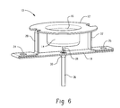
FIG. 6 is a perspective view illustrating the dual band antenna of FIG. 2 coupled to a coaxial cable.
FIG. 7 illustrates a perspective view of a dual band antenna of FIG. 1 mounted to an external ground plane.
FIG. 8 illustrates an example methodology for forming a dual band antenna from a single piece of metal.
OVERVIEW OF EXAMPLE EMBODIMENTS
The following presents a simplified overview of the example embodiments in order to provide a basic understanding of some aspects of the example embodiments. This overview is not an extensive overview of the example embodiments. It is intended to neither identify key or critical elements of the example embodiments nor delineate the scope of the appended claims. Its sole purpose is to present some concepts of the example embodiments in a simplified form as a prelude to the more detailed description that is presented later.
In accordance with an example embodiment, there is disclosed herein, an apparatus, comprising a circular patch antenna and a cylindrical matching element coupled to the circular patch antenna configured to provide a desired impedance at a predetermined frequency. A feed surface is coupled to the cylindrical element.
In accordance with an example embodiment, there is disclosed herein, a method comprising forming a circular patch antenna from a piece of metal. A cylindrical matching element is formed below the patch antenna. A feed surface is formed at the bottom of the cylindrical matching element.
DESCRIPTION OF EXAMPLE EMBODIMENTS
This description provides examples not intended to limit the scope of the appended claims. The figures generally indicate the features of the examples, where it is understood and appreciated that like reference numerals are used to refer to like elements. Reference in the specification to “one embodiment” or “an embodiment” or “an example embodiment” means that a particular feature, structure, or characteristic described is included in at least one embodiment described herein and does not imply that the feature, structure, or characteristic is present in all embodiments described herein.
Described in an example embodiment herein is a dual band antenna that comprises a circular patch antenna operating in a TMO2 mode. Shorting pins and a cylindrical matching element are included to provide the appropriate impedance for the desired bands, for example the 2.4 GHz and 5 GHz bands. In particular embodiments, the antenna is formed with one piece of metal and includes a feed tab and a solder cup for use with thin coaxial cables.
Referring to FIG. 1, there is illustrated an example of a dual band antenna 10. Antenna 10 comprises a circular patch mode antenna 12 and a cylindrical matching element 14. Circular patch mode antenna 12 can be tuned (e.g. the appropriate size, such as diameter is selected for a first desired band) to a first operating band. The depth, e.g., the distance between circular patch mode antenna 12 and bottom surface 32, and/or diameter of cylindrical matching element 14 can be selected to provide the appropriate impedance at a second desired band. A feed surface, such as a pin, 28 is coupled to cylindrical matching element 14.
In particular embodiments, as will be described in more detail herein, there is an aperture 16 on the surface of circular patch mode antenna 12 corresponding to the diameter of cylindrical matching element 14. In an example embodiment this aperture 16 is aligned with the cylindrical matching element 14. Antenna 10 further comprises shorting strips 20, 22 coupled to tabs 24, 26 which can be employed to couple antenna 10 to a ground plane (see for example FIG. 7).
Referring now to FIGS. 2-5 with continued reference to FIG. 1, ground plane 18 is coupled to circular patch mode antenna 12 by shorting strips 20, 22. In an example embodiment, tabs 24, 26 are employed to couple strips 20, 22 to ground plane 18. A feed surface 28 is located on a bottom surface 32 of cylindrical matching element 14. Solder cup 30 is formed on grounding plane 18 and can be aligned with feed surface 28.
In an example embodiment, shorting pins 20, 22 are employed to load circular patch antenna 12. As those skilled in the art can readily appreciate, loading can be employed as a means to broadband an antenna, shrink the size of an antenna, control polarization, or otherwise influence the mode of operation. In an example embodiment, thin metal cylinders can be employed for shorting pins 20, 22. In another example embodiment, as will be described herein infra, shorting pins may be formed from a single piece of metal used to form circular patch antenna 12 and ground plane 18. In the illustrated example, two shorting pins 20, 22 are employed. In particular embodiments, shorting pins 20, 22 are symmetrical about the center 34 of circular patch antenna 12.
For example, without shorting pins, a TMO2 patch antenna for the 2.4 GHz band would be about 75 millimeters (mm) in diameter. With shorting pins 20, 22, the size of a TMO2 patch antenna for the 2.4 GHz band can be reduced to about 29 mm and located about 10 mm above ground plane 18. The width of shorting pins 20, 22 can be selected to duplicate the performance that would be provided by cylindrical shorting pins.
A cylindrical matching element 14 is designed to provide the proper impedance over a second band. For example, for an antenna operating in the 2.4 GHz and 5 GHz bands, cylindrical matching element 14 is designed to provide the proper impedance, for example 50 ohms. In an example embodiment, cylindrical matching element 14 is coupled to cylindrical patch antenna 12 and feed surface 28. In an example embodiment, the diameter and the depth (or length) of cylindrical matching element, which is the distance from circular patch antenna 12 and bottom surface 32 is selected to provide the appropriate impedance at the second band.
In an example embodiment, because cylindrical matching element 14 is coupled to circular patch antenna 12, there are no fields below circular patch antenna 12 inside of cylindrical matching element 14. Therefore, the portion of circular patch antenna 12 that is inside of cylindrical matching element 14 may be removed, forming aperture 16. This enables a single piece of metal to be used to form circular patch antenna 12, cylindrical matching element 14, and shorting pins 20, 22. Shorting pins 20, 22 may be realized by bending metal flaps along the annular surface of circular patch antenna 12. Shorting pins 20, 22 may be attached to a ground plane, for example on a surface of an access point, which is illustrated in FIG. 6. In particular embodiments, one of the flaps may be longer than the other (for example the flap forming strip 22 in FIG. 1 is longer than the flap forming strip 20). The longer flap can have additional bends, including a 180 degree bend 38 to form ground strip or ground plane 18 illustrated in FIG. 1. This ensures that the entire antenna can be built from a single metal piece rather than a combination of two or more pieces.
FIG. 6 illustrates an example of a coaxial cable 36 coupled to antenna 10. The cable is passed through solder cup 30. The outer conductor of the coaxial cable (not shown) can be coupled to ground strip or plane 18 while the inner conductor (not shown) of the coaxial cable can be provided to feed surface 28.
In view of the foregoing structural and functional features described above, a methodology 800 in accordance with an example embodiment will be better appreciated with reference to FIG. 8. While, for purposes of simplicity of explanation, methodology 800 is shown and described as executing serially, it is to be understood and appreciated that the example embodiment is not limited by the illustrated order, as some aspects could occur in different orders and/or concurrently with other aspects from that shown and described herein. Moreover, not all illustrated features may be required to implement methodology 800 in accordance with an aspect of an example embodiment.
At 802, a circular patch antenna is formed. The diameter of the circular patch antenna is selected to operate at a first predetermined band.
At 804, a cylindrical matching element is formed. In an example embodiment, the cylindrical matching element is formed below the circular patch antenna. In an example embodiment, a feed surface, such as a pin is formed on the bottom surface of the cylindrical matching element. The cylindrical matching element may be designed in a ‘cup’ shape where the circular patch antenna is at the top of the cup and a feed surface such as a pin is located at the bottom (or opposite) surface. The depth (the distance from the circular patch antenna to opposite side of the cylindrical matching element) and diameter of the cylindrical matching element may be selected to provide the appropriate impedance for a second predetermined band.
At 806, a tab coupled to the circular patch antenna is bent to form a first shorting pin. Additional bends are employed to provide a ground strip or ground plane. In particular embodiments, a 180 degree bend is employed so that the ground plane passes underneath the cylindrical matching element.
At 808, a second tab coupled to the circular patch antenna is bent to form a second shorting pin. The second shorting pin is coupled to the ground plane. The widths of the first and second shorting pins can be selected to provide the performance that would be realized by employing cylindrical shorting pins. The first and second shorting pins may be coupled to the ground plane using any appropriate means, such as screws, rivets, solder, etc.
At 810, a solder cup is formed on the ground plane. In an example embodiment, the solder cup is aligned with the feed surface located on the cylindrical matching element. In particular embodiments, the solder cup, and feed surface are aligned with the center of the circular patch antenna.
Described above are example embodiments. It is, of course, not possible to describe every conceivable combination of components or methodologies, but one of ordinary skill in the art will recognize that many further combinations and permutations of the example embodiments are possible. Accordingly, this application is intended to embrace all such alterations, modifications and variations that fall within the spirit and scope of the appended claims interpreted in accordance with the breadth to which they are fairly, legally and equitably entitled.

Claims (20)

The invention claimed is:
1. An apparatus, comprising:
a metal circular patch antenna tuned for a first band defining an aperture;
a hollow cup-shaped cylindrical matching element having a top end, a cylindrical middle portion, and a bottom end, formed below the circular patch antenna in a first direction, the cylindrical middle portion having a diameter,
wherein the circular patch antenna is coupled with the top end of the cup-shaped cylindrical matching element,
wherein a first diameter of the top end is aligned with the aperture of the patch antenna, and a second diameter of the top end is aligned with the diameter of the cylindrical middle portion,
wherein the diameter of the cylindrical middle portion and a depth of the cylindrical matching element defined by a distance along the first direction between upper and lower ends of the matching element are configured to provide a desired impedance for a second band;
a feed surface coupled with the cylindrical matching element;
a ground plane;
and a pair of generally planar shorting pins coupling the circular patch antenna with the ground plane in a generally perpendicular orientation therebetween.
2. The apparatus set forth in claim 1, wherein the hollow cup-shaped cylindrical matching element is aligned with a center of the circular patch antenna.
3. The apparatus set forth in claim 1 wherein the shorting pins are disposed radially from a surface of the circular patch antenna and outwardly of the matching element.
4. The apparatus set forth in claim 3, wherein the pair of shorting pins are disposed symmetrically about a center of the circular patch antenna.
5. The apparatus set forth in claim 4, wherein the shorting pins are riveted to the ground plane.
6. The apparatus set forth in claim 4, wherein the ground plane has a solder cup aligned with the feed surface.
7. The apparatus set forth in claim 1, wherein:
the patch antenna comprises a continuous annular surface having an outer diameter and an inner diameter that defines the aperture; and
the first diameter of the top end matches the inner diameter of the annular surface of the patch antenna.
8. The apparatus set forth in claim 1, wherein the depth of the cylindrical matching element corresponds to operate the circular patch antenna at the second frequency.
9. The apparatus set forth in claim 1, wherein the circular patch antenna, the cylindrical matching element, and the feed surface are formed from a single piece of metal.
10. A method, comprising:
forming a circular patch antenna from a piece of metal, the circular patch antenna defining an aperture in the piece of metal;
forming a hollow cup-shaped cylindrical matching element having a top end, a cylindrical middle portion, and a bottom end, from the piece of metal below the patch antenna in a first direction, the cylindrical middle portion having a diameter,
wherein the circular patch antenna is coupled with the top end of the cup-shaped cylindrical matching element,
wherein a first diameter of the top end is aligned with the aperture of the patch antenna, and a second diameter of the top end is aligned with the diameter of the cylindrical middle portion,
wherein the diameter of the cylindrical middle portion and a depth of the cylindrical matching element defined by a distance along the first direction between upper and lower ends of the matching element are configured to provide a desired impedance for a second band;
forming a ground plane and a first shorting pin between the circular patch antenna and the ground plane;
forming a feed surface at the bottom of the cylindrical matching element; and
forming a second shorting pin coupling the circular patch antenna with the ground plane in a generally perpendicular orientation therebetween.
11. The method of claim 10, further comprising bending the piece of metal to form the ground plane and the first shorting pin between the circular patch antenna and the ground plane and forming the shorting pin so as to be disposed radially from a surface of the circular patch antenna and outwardly of the matching element.
12. The method of claim 11, further comprising bending the piece of metal at a second location to form the second shorting pin between the circular patch antenna and the ground plane and forming the second shorting pin so as to be disposed radially from a surface of the circular patch antenna.
13. The method of claim 12, further comprising riveting the first and second shorting pins to the ground plane.
14. The method of claim 12, wherein the first and second pins are disposed symmetrically about a center of the cylindrical patch antenna.
15. The method of claim 11, further comprising forming a solder cup in the ground plane.
16. The method of claim 15, further comprising forming the solder cup underneath the feed surface.
17. The method of claim 11, wherein the depth of the cylindrical matching element corresponds to a selected operating frequency of the second band.
18. The method of claim 11, wherein:
the forming the patch antenna comprises forming a continuous annular surface having an outer diameter and an inner diameter that defines the aperture, wherein the first diameter of the top end matches the inner diameter of the annular surface of the patch antenna.
19. The method of claim 11, wherein the circular patch antenna is formed for operating in a TM02 mode.
20. The method of claim 11, wherein the cylindrical matching element is formed for 50 ohm operation at a predetermined band.
US12/837,156 2010-07-15 2010-07-15 Dual band antenna design Active 2031-09-07 US8963793B2 (en)

Priority Applications (1)

Application Number Priority Date Filing Date Title
US12/837,156 US8963793B2 (en) 2010-07-15 2010-07-15 Dual band antenna design

Applications Claiming Priority (1)

Application Number Priority Date Filing Date Title
US12/837,156 US8963793B2 (en) 2010-07-15 2010-07-15 Dual band antenna design

Publications (2)

Publication Number Publication Date
US20120013521A1 US20120013521A1 (en) 2012-01-19
US8963793B2 true US8963793B2 (en) 2015-02-24

Family

ID=45466544

Family Applications (1)

Application Number Title Priority Date Filing Date
US12/837,156 Active 2031-09-07 US8963793B2 (en) 2010-07-15 2010-07-15 Dual band antenna design

Country Status (1)

Country Link
US (1) US8963793B2 (en)

Cited By (7)

* Cited by examiner, † Cited by third party
Publication number Priority date Publication date Assignee Title
US20170288299A1 (en) * 2014-10-07 2017-10-05 Denso Corporation Antenna device
US10186775B2 (en) 2015-08-11 2019-01-22 The United States Of America, As Represented By The Secretary Of The Army Patch antenna element with parasitic feed probe
EP3460904A1 (en) 2017-09-20 2019-03-27 PC-Tel, Inc. Capacitively-coupled dual-band antenna
US10693235B2 (en) 2018-01-12 2020-06-23 The Government Of The United States, As Represented By The Secretary Of The Army Patch antenna elements and parasitic feed pads
US10868584B2 (en) * 2017-02-21 2020-12-15 Samsung Electronics Co., Ltd. Antenna device and electronic device including same
US10971803B2 (en) 2019-08-14 2021-04-06 Cisco Technology, Inc. Omnidirectional antenna system for macro-macro cell deployment with concurrent band operation
US11264717B2 (en) 2017-06-13 2022-03-01 Huawei Technologies Co., Ltd. Dual-band antenna, wireless local area network device, and method for manufacturing dual-band antenna

Families Citing this family (9)

* Cited by examiner, † Cited by third party
Publication number Priority date Publication date Assignee Title
CN102931485B (en) * 2012-11-12 2014-07-23 深圳市首达电子有限公司 Multi-functional wireless fidelity (WiFi) device
US9450292B2 (en) * 2013-06-05 2016-09-20 Apple Inc. Cavity antennas with flexible printed circuits
CN104347937B (en) * 2013-07-24 2018-01-05 深圳光启尖端技术有限责任公司 Three-dimensional antenna, communication system, aircraft and means of transport
US9917370B2 (en) 2014-04-04 2018-03-13 Cisco Technology, Inc. Dual-band printed omnidirectional antenna
US9748654B2 (en) * 2014-12-16 2017-08-29 Laird Technologies, Inc. Antenna systems with proximity coupled annular rectangular patches
JP6523846B2 (en) * 2015-07-22 2019-06-05 日本電産サンキョー株式会社 Communication device, contactless card reader, and wireless system
US10148002B2 (en) * 2016-05-09 2018-12-04 Cisco Technology, Inc. Horizontally-polarized antenna for microcell coverage having high isolation
EP3422473B1 (en) * 2017-06-30 2021-07-28 GN Audio A/S Antenna structure for a headset
CN109088153B (en) * 2018-08-03 2021-01-01 瑞声精密制造科技(常州)有限公司 Ultra-wideband MIMO antenna and terminal

Citations (5)

* Cited by examiner, † Cited by third party
Publication number Priority date Publication date Assignee Title
US20030210193A1 (en) * 2002-05-13 2003-11-13 Rossman Court Emerson Low Profile Two-Antenna Assembly Having a Ring Antenna and a Concentrically-Located Monopole Antenna
US20040021606A1 (en) * 2002-07-11 2004-02-05 Alps Electric Co., Ltd. Small plane antenna and composite antenna using the same
US20090102723A1 (en) * 2007-10-18 2009-04-23 Mateychuk Duane N Dual moded stacked microstrip patch antenna
US20090128442A1 (en) * 2006-08-24 2009-05-21 Seiken Fujita Antenna apparatus
US7692601B2 (en) * 2002-12-13 2010-04-06 Andrew Llc Dipole antennas and coaxial to microstrip transitions

Patent Citations (6)

* Cited by examiner, † Cited by third party
Publication number Priority date Publication date Assignee Title
US20030210193A1 (en) * 2002-05-13 2003-11-13 Rossman Court Emerson Low Profile Two-Antenna Assembly Having a Ring Antenna and a Concentrically-Located Monopole Antenna
US6812902B2 (en) * 2002-05-13 2004-11-02 Centurion Wireless Technologies, Inc. Low profile two-antenna assembly having a ring antenna and a concentrically-located monopole antenna
US20040021606A1 (en) * 2002-07-11 2004-02-05 Alps Electric Co., Ltd. Small plane antenna and composite antenna using the same
US7692601B2 (en) * 2002-12-13 2010-04-06 Andrew Llc Dipole antennas and coaxial to microstrip transitions
US20090128442A1 (en) * 2006-08-24 2009-05-21 Seiken Fujita Antenna apparatus
US20090102723A1 (en) * 2007-10-18 2009-04-23 Mateychuk Duane N Dual moded stacked microstrip patch antenna

Cited By (12)

* Cited by examiner, † Cited by third party
Publication number Priority date Publication date Assignee Title
US20170288299A1 (en) * 2014-10-07 2017-10-05 Denso Corporation Antenna device
US10461403B2 (en) * 2014-10-07 2019-10-29 Denso Corporation Antenna device
US10186775B2 (en) 2015-08-11 2019-01-22 The United States Of America, As Represented By The Secretary Of The Army Patch antenna element with parasitic feed probe
US10868584B2 (en) * 2017-02-21 2020-12-15 Samsung Electronics Co., Ltd. Antenna device and electronic device including same
US11264717B2 (en) 2017-06-13 2022-03-01 Huawei Technologies Co., Ltd. Dual-band antenna, wireless local area network device, and method for manufacturing dual-band antenna
EP3460904A1 (en) 2017-09-20 2019-03-27 PC-Tel, Inc. Capacitively-coupled dual-band antenna
CN109659675A (en) * 2017-09-20 2019-04-19 Pc-Tel公司 Double frequency band aerial
US10498047B1 (en) 2017-09-20 2019-12-03 Pc-Tel, Inc. Capacitively-coupled dual-band antenna
CN109659675B (en) * 2017-09-20 2020-11-06 Pc-Tel公司 Dual-band antenna
US10693235B2 (en) 2018-01-12 2020-06-23 The Government Of The United States, As Represented By The Secretary Of The Army Patch antenna elements and parasitic feed pads
US10879613B2 (en) 2018-01-12 2020-12-29 The Government Of The United States, As Represented By The Secretary Of The Army Patch antenna elements and parasitic feed pads
US10971803B2 (en) 2019-08-14 2021-04-06 Cisco Technology, Inc. Omnidirectional antenna system for macro-macro cell deployment with concurrent band operation

Also Published As

Publication number Publication date
US20120013521A1 (en) 2012-01-19

Similar Documents

Publication Publication Date Title
US8963793B2 (en) Dual band antenna design
US9252490B2 (en) Multi-band antenna and electronic device provided with the same
US7385563B2 (en) Multiple antenna array with high isolation
US8866691B2 (en) Multimode antenna structure
US7271769B2 (en) Antennas encapsulated within plastic display covers of computing devices
US7339543B2 (en) Array antenna with low profile
EP3172797B1 (en) Slot antenna
EP3201986B1 (en) Antenna device for a base station antenna system
EP2509158B1 (en) Communication electronic device and antenna structure thereof
CA2643166A1 (en) Slit loaded tapered slot patch antenna
JP5738246B2 (en) Dual polarization antenna
US9425498B2 (en) Wideband antenna module
CN102918705A (en) Dual-polarization radiating element of a multiband antenna
US7466272B1 (en) Dual-band antenna
KR20150110291A (en) Multiband hybrid antenna
EP2808942B1 (en) Antenna structure
US20170170555A1 (en) Decoupled Antennas For Wireless Communication
EP3439102A1 (en) One-piece dual-band antenna and ground plane
US10439289B2 (en) Wide-band antenna
US20090015506A1 (en) Planar antenna
KR101632275B1 (en) Multiband 2-port antenna
EP3312934B1 (en) Antenna
US20120154230A1 (en) Multi-band antenna
US10680661B2 (en) Monopole and slot antenna assembly
US11233322B2 (en) Communication device

Legal Events

Date Code Title Description
AS Assignment

Owner name: CISCO TECHNOLOGY, INC., CALIFORNIA

Free format text: ASSIGNMENT OF ASSIGNORS INTEREST;ASSIGNORS:SALIGA, STEPHEN V.;LUTMAN, THOMAS G.;REEL/FRAME:024692/0835

Effective date: 20100715

STCF Information on status: patent grant

Free format text: PATENTED CASE

MAFP Maintenance fee payment

Free format text: PAYMENT OF MAINTENANCE FEE, 4TH YEAR, LARGE ENTITY (ORIGINAL EVENT CODE: M1551); ENTITY STATUS OF PATENT OWNER: LARGE ENTITY

Year of fee payment: 4

MAFP Maintenance fee payment

Free format text: PAYMENT OF MAINTENANCE FEE, 8TH YEAR, LARGE ENTITY (ORIGINAL EVENT CODE: M1552); ENTITY STATUS OF PATENT OWNER: LARGE ENTITY

Year of fee payment: 8