US8972761B2 - Systems and methods for idle clock insertion based power control - Google Patents
Systems and methods for idle clock insertion based power control Download PDFInfo
- Publication number
- US8972761B2 US8972761B2 US13/364,217 US201213364217A US8972761B2 US 8972761 B2 US8972761 B2 US 8972761B2 US 201213364217 A US201213364217 A US 201213364217A US 8972761 B2 US8972761 B2 US 8972761B2
- Authority
- US
- United States
- Prior art keywords
- data
- circuit
- clock
- data processing
- algorithm
- Prior art date
- Legal status (The legal status is an assumption and is not a legal conclusion. Google has not performed a legal analysis and makes no representation as to the accuracy of the status listed.)
- Active, expires
Links
Images


Classifications
-
- G—PHYSICS
- G06—COMPUTING; CALCULATING OR COUNTING
- G06F—ELECTRIC DIGITAL DATA PROCESSING
- G06F1/00—Details not covered by groups G06F3/00 - G06F13/00 and G06F21/00
- G06F1/26—Power supply means, e.g. regulation thereof
- G06F1/32—Means for saving power
- G06F1/3203—Power management, i.e. event-based initiation of a power-saving mode
- G06F1/3234—Power saving characterised by the action undertaken
- G06F1/324—Power saving characterised by the action undertaken by lowering clock frequency
-
- G—PHYSICS
- G06—COMPUTING; CALCULATING OR COUNTING
- G06F—ELECTRIC DIGITAL DATA PROCESSING
- G06F1/00—Details not covered by groups G06F3/00 - G06F13/00 and G06F21/00
- G06F1/26—Power supply means, e.g. regulation thereof
- G06F1/32—Means for saving power
- G06F1/3203—Power management, i.e. event-based initiation of a power-saving mode
- G06F1/3234—Power saving characterised by the action undertaken
- G06F1/325—Power saving in peripheral device
- G06F1/3268—Power saving in hard disk drive
-
- G—PHYSICS
- G11—INFORMATION STORAGE
- G11B—INFORMATION STORAGE BASED ON RELATIVE MOVEMENT BETWEEN RECORD CARRIER AND TRANSDUCER
- G11B19/00—Driving, starting, stopping record carriers not specifically of filamentary or web form, or of supports therefor; Control thereof; Control of operating function ; Driving both disc and head
- G11B19/02—Control of operating function, e.g. switching from recording to reproducing
-
- G—PHYSICS
- G11—INFORMATION STORAGE
- G11B—INFORMATION STORAGE BASED ON RELATIVE MOVEMENT BETWEEN RECORD CARRIER AND TRANSDUCER
- G11B19/00—Driving, starting, stopping record carriers not specifically of filamentary or web form, or of supports therefor; Control thereof; Control of operating function ; Driving both disc and head
- G11B19/20—Driving; Starting; Stopping; Control thereof
- G11B19/209—Driving; Starting; Stopping; Control thereof in multiple disk arrays, e.g. spindle synchronisation in RAID systems
-
- Y—GENERAL TAGGING OF NEW TECHNOLOGICAL DEVELOPMENTS; GENERAL TAGGING OF CROSS-SECTIONAL TECHNOLOGIES SPANNING OVER SEVERAL SECTIONS OF THE IPC; TECHNICAL SUBJECTS COVERED BY FORMER USPC CROSS-REFERENCE ART COLLECTIONS [XRACs] AND DIGESTS
- Y02—TECHNOLOGIES OR APPLICATIONS FOR MITIGATION OR ADAPTATION AGAINST CLIMATE CHANGE
- Y02D—CLIMATE CHANGE MITIGATION TECHNOLOGIES IN INFORMATION AND COMMUNICATION TECHNOLOGIES [ICT], I.E. INFORMATION AND COMMUNICATION TECHNOLOGIES AIMING AT THE REDUCTION OF THEIR OWN ENERGY USE
- Y02D10/00—Energy efficient computing, e.g. low power processors, power management or thermal management
Definitions
- the present inventions are related to systems and methods for data processing, and more particularly to systems and methods for power governance in a data processing system.
- Various data transfer systems have been developed including storage systems, cellular telephone systems, radio transmission systems.
- data is transferred from a sender to a receiver via some medium.
- data is sent from a sender (i.e., a write function) to a receiver (i.e., a read function) via a storage medium.
- the data processing function uses a variable number of iterations depending upon the characteristics of the data being processed. The variable number of processing iterations result in ambiguity in determining circuit power requirements, and can require the choice of an expensive packaging designed to dissipate power at a higher rate than may actually be required.
- the present inventions are related to systems and methods for data processing, and more particularly to systems and methods for power governance in a data processing system.
- Various embodiments of the present invention provide data processing systems that include a first data processing circuit, a second data processing circuit, and an idle time enforcement circuit.
- the first data processing circuit is operable to process a data input synchronous to a first clock
- the second data processing circuit is operable to process an output derived from the first data processing circuit synchronous to a second clock.
- the idle time enforcement circuit is operable to determine that the first data processing circuit and the second data processing circuit are concurrently operational, and based at least in part on determining that the first data processing circuit and the second data processing circuit are concurrently operational, to modify an average frequency of at least one of the first clock and the second clock.
- only the first clock is modified.
- only the second clock is modified.
- the first clock and the second clock operate at the same frequency.
- the system is implemented as an integrated circuit.
- the data processing system is incorporated in a storage device, or a data transmission device.
- modifying the average frequency of at least one of the first clock and the second clock includes suppressing one clock cycle for each N clock cycles.
- N is four. In other cases, N is eight. In various cases, N is user programmable.
- the first data processing circuit is a data detector circuit operable to apply a data detection algorithm to the data input.
- data detector circuits may be, but are not limited to, a Viterbi algorithm data detector circuit, or a maximum a posteriori data detector circuit.
- the second data processing circuit is a low density parity check decoder circuit.
- the system further includes a power monitor circuit operable to determine whether a power usage exceeds a threshold, and to assert a power status signal indicating that the power usage level exceeds the threshold.
- the idle time enforcement circuit is operable to modify an average frequency of at least one of the first clock and the second clock based at least in part on a combination of the first data processing circuit and the second data processing circuit concurrently operating, and assertion of the power status signal.
- Other embodiments of the present invention provide methods for data processing that include: providing a data detector circuit; providing a data decoder circuit; applying a data detection algorithm synchronous to a first clock to a data input by the data detector circuit to yield a first detected output; applying a data decode algorithm synchronous to a second clock to a decode input derived from a second detected output to yield a decode output; determining that the data detector circuit is applying the data detection algorithm concurrent with applying the data decode algorithm; and based at least in part on the determination that the data detector circuit is applying the data detection algorithm concurrent with applying the data decode algorithm, reducing an average frequency of at least one of the first clock and the second clock.
- FIG. 1 shows a storage system including idle time enforcement circuitry in accordance with various embodiments of the present invention
- FIG. 2 depicts a data transmission system including idle time enforcement circuitry in accordance with one or more embodiments of the present invention
- FIG. 3 shows a data processing circuit including an idle time enforcement circuit in accordance with some embodiments of the present invention
- FIG. 4 a is a flow diagram showing a method for variable data processing through data decoder and data detection circuitry
- FIG. 4 b is a flow diagram showing a method for enforcing idle time in conjunction with the method of FIG. 4 a in accordance with some embodiments of the present invention
- FIG. 4 c is a flow diagram showing another method for enforcing idle time in conjunction with the method of FIG. 4 a in accordance with other embodiments of the present invention.
- FIGS. 5 a - 5 b are timing diagrams showing idle time enforcement described in FIGS. 4 a - 4 b at different values of N;
- FIGS. 6 a - 6 c graphically show processing changes due to different idle time enforcement described in relation to FIGS. 4 a - 4 b.
- the present inventions are related to systems and methods for data processing, and more particularly to systems and methods for power governance in a data processing system.
- a variable data processing system may include one or more data detector circuits and one or more data decoder circuits with the output of a data detector circuit being passed to a data decoder circuit for processing.
- a data decoder circuit for processing may include one or more data detector circuits and one or more data decoder circuits with the output of a data detector circuit being passed to a data decoder circuit for processing.
- At various operational times one or more of the data detector circuits and one or more of the decoder circuits are processing at the same time. This may result in excessive power usage.
- the embodiments of the present invention provide for idle time enforcement to mitigate power usage.
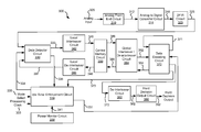
- Storage system 100 may be, for example, a hard disk drive.
- Storage system 100 also includes a preamplifier 170 , an interface controller 120 , a hard disk controller 166 , a motor controller 168 , a spindle motor 172 , a disk platter 178 , and a read/write head 176 .
- Interface controller 120 controls addressing and timing of data to/from disk platter 178 .
- the data on disk platter 178 consists of groups of magnetic signals that may be detected by read/write head assembly 176 when the assembly is properly positioned over disk platter 178 .
- disk platter 178 includes magnetic signals recorded in accordance with either a longitudinal or a perpendicular recording scheme.
- read/write head assembly 176 is accurately positioned by motor controller 168 over a desired data track on disk platter 178 .
- Motor controller 168 both positions read/write head assembly 176 in relation to disk platter 178 and drives spindle motor 172 by moving read/write head assembly to the proper data track on disk platter 178 under the direction of hard disk controller 166 .
- Spindle motor 172 spins disk platter 178 at a determined spin rate (RPMs).
- the sensed magnetic signals are provided as a continuous, minute analog signal representative of the magnetic data on disk platter 178 .
- This minute analog signal is transferred from read/write head assembly 176 to read channel circuit 110 via preamplifier 170 .
- Preamplifier 170 is operable to amplify the minute analog signals accessed from disk platter 178 .
- read channel circuit 110 decodes and digitizes the received analog signal to recreate the information originally written to disk platter 178 .
- This data is provided as read data 103 to a receiving circuit.
- a write operation is substantially the opposite of the preceding read operation with write data 101 being provided to read channel circuit 110 .
- This data is then encoded and written to disk platter 178 .
- read channel circuit 110 utilizes a variable data processing circuit that allows different portions of data to utilize different amounts of processing bandwidth and different combinations of data detector and/or data decoder circuits. Where too many data decoding or data detection circuits are used at the same time, an over current condition may occur. To avoid this over current condition, idle time is enforced in a data detection circuit, a data decoding circuit, or both a data detection circuit and a data decoding circuit. This idle time reduces the processing bandwidth of the affected circuits and at the same time reduces current demands of storage system 100 .
- Read channel circuit 110 may be implemented to include a data processing circuit similar to that discussed below in relation to FIG. 3 . Further, the enforcement of the idle time may be accomplished consistent with one of the approaches discussed below in relation to FIGS. 4 a - 4 c.
- storage system 100 may be integrated into a larger storage system such as, for example, a RAID (redundant array of inexpensive disks or redundant array of independent disks) based storage system.
- RAID redundant array of inexpensive disks or redundant array of independent disks
- Such a RAID storage system increases stability and reliability through redundancy, combining multiple disks as a logical unit.
- Data may be spread across a number of disks included in the RAID storage system according to a variety of algorithms and accessed by an operating system as if it were a single disk. For example, data may be mirrored to multiple disks in the RAID storage system, or may be sliced and distributed across multiple disks in a number of techniques.
- the disks in the RAID storage system may be, but are not limited to, individual storage systems such as storage system 100 , and may be located in close proximity to each other or distributed more widely for increased security.
- write data is provided to a controller, which stores the write data across the disks, for example by mirroring or by striping the write data.
- the controller retrieves the data from the disks. The controller then yields the resulting read data as if the RAID storage system were a single disk.
- Data transmission system 291 including a receiver 295 having idle time enforcement circuitry is shown in accordance with various embodiments of the present invention.
- Data transmission system 291 includes a transmitter 293 that is operable to transmit encoded information via a transfer medium 297 as is known in the art.
- the encoded data is received from transfer medium 297 by a receiver 295 .
- Receiver 295 processes the received input to yield the originally transmitted data.
- receiver 295 utilizes a variable data processing circuit that allows different chunks of data to utilize different amounts of processing bandwidth and utilizing different combinations of data detector and/or data decoder circuits. Where too many data decoding or data detection circuits are used at the same time, an over current condition may occur.
- idle time is enforced in a data detection circuit, a data decoding circuit, or both a data detection circuit and a data decoding circuit. This idle time reduces the processing bandwidth of the affected circuits and at the same time reduces current demands of receiver 295 .
- Receiver 295 may be implemented to include a data processing circuit similar to that discussed below in relation to FIG. 3 . Further, the enforcement of the idle time may be accomplished consistent with one of the approaches discussed below in relation to FIGS. 4 a - 4 c.
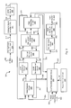
- FIG. 3 shows a data processing circuit 300 including an idle time enforcement circuit 339 in accordance with some embodiments of the present invention.
- Data processing circuit 300 includes an analog front end circuit 310 that receives an analog signal 305 .
- Analog front end circuit 310 processes analog signal 305 and provides a processed analog signal 312 to an analog to digital converter circuit 314 .
- Analog front end circuit 310 may include, but is not limited to, an analog filter and an amplifier circuit as are known in the art. Based upon the disclosure provided herein, one of ordinary skill in the art will recognize a variety of circuitry that may be included as part of analog front end circuit 310 .
- analog signal 305 is derived from a read/write head assembly (not shown) that is disposed in relation to a storage medium (not shown).
- analog signal 305 is derived from a receiver circuit (not shown) that is operable to receive a signal from a transmission medium (not shown).
- the transmission medium may be wired or wireless.
- Analog to digital converter circuit 314 converts processed analog signal 312 into a corresponding series of digital samples 316 .
- Analog to digital converter circuit 314 may be any circuit known in the art that is capable of producing digital samples corresponding to an analog input signal. Based upon the disclosure provided herein, one of ordinary skill in the art will recognize a variety of analog to digital converter circuits that may be used in relation to different embodiments of the present invention.
- Digital samples 316 are provided to an equalizer circuit 320 .
- Equalizer circuit 320 applies an equalization algorithm to digital samples 316 to yield an equalized output 325 .
- equalizer circuit 320 is a digital finite impulse response filter circuit as are known in the art.
- equalizer 320 includes sufficient memory to maintain one or more codewords until processing of that codeword is completed through a data detector circuit 330 and a data decoding circuit 370 including, where warranted, multiple global iterations (passes through both data detector circuit 330 and data decoding circuit 370 ) and/or local iterations (passes through data decoding circuit 370 during a given global iteration). It may be possible that equalized output 325 may be received directly from a storage device in, for example, a solid state storage system. In such cases, analog front end circuit 310 , analog to digital converter circuit 314 and equalizer circuit 320 may be eliminated where the data is received as a digital data input.
- Data detector circuit 330 may be a single data detector circuit or may be two or more data detector circuits operating in parallel on different codewords. Whether it is a single data detector circuit or a number of data detector circuits operating in parallel, data detector circuit 330 is operable to apply a data detection algorithm to a received codeword or data set. In some embodiments of the present invention, data detector circuit 330 is a Viterbi algorithm data detector circuit as are known in the art. In other embodiments of the present invention, data detector circuit 330 is a is a maximum a posteriori data detector circuit as are known in the art.
- Viterbi data detection algorithm or “Viterbi algorithm data detector circuit” are used in their broadest sense to mean any Viterbi detection algorithm or Viterbi algorithm detector circuit or variations thereof including, but not limited to, bi-direction Viterbi detection algorithm or bi-direction Viterbi algorithm detector circuit.
- maximum a posteriori data detection algorithm or “maximum a posteriori data detector circuit” are used in their broadest sense to mean any maximum a posteriori detection algorithm or detector circuit or variations thereof including, but not limited to, simplified maximum a posteriori data detection algorithm and a max-log maximum a posteriori data detection algorithm, or corresponding detector circuits.
- one data detector circuit included in data detector circuit 330 is used to apply the data detection algorithm to the received codeword for a first global iteration applied to the received codeword, and another data detector circuit included in data detector circuit 330 is operable apply the data detection algorithm to the received codeword guided by a decoded output accessed from a central memory circuit 350 on subsequent global iterations.
- Detector output 333 includes soft data.
- soft data is used in its broadest sense to mean reliability data with each instance of the reliability data indicating a likelihood that a corresponding bit position or group of bit positions has been correctly detected.
- the soft data or reliability data is log likelihood ratio data as is known in the art.
- Detected output 333 is provided to a local interleaver circuit 342 .
- Local interleaver circuit 342 is operable to shuffle sub-portions (i.e., local chunks) of the data set included as detected output and provides an interleaved codeword 346 that is stored to central memory circuit 350 .
- Interleaver circuit 342 may be any circuit known in the art that is capable of shuffling data sets to yield a re-arranged data set.
- Interleaved codeword 346 is stored to central memory circuit 350 .
- Global interleaver/De-interleaver circuit 384 may be any circuit known in the art that is capable of globally rearranging codewords.
- Global interleaver/De-interleaver circuit 384 provides a decoder input 352 into data decoding circuit 370 .
- the data decode algorithm is a low density parity check algorithm as are known in the art.
- Data decoding circuit 370 applies a data decode algorithm to decoder input 352 to yield a decoded output 371 .
- data decoding circuit 370 re-applies the data decode algorithm to decoder input 352 guided by decoded output 371 . This continues until either a maximum number of local iterations is exceeded or decoded output 371 converges.
- decoded output 371 fails to converge (i.e., fails to yield the originally written data set) and a number of local iterations through data decoder circuit 370 exceeds a threshold
- the resulting decoded output is provided as a decoded output 354 back to central memory circuit 350 where it is stored awaiting another global iteration through a data detector circuit included in data detector circuit 330 .
- decoded output 354 Prior to storage of decoded output 354 to central memory circuit 350 , decoded output 354 is globally de-interleaved to yield a globally de-interleaved output 388 that is stored to central memory circuit 350 .
- the global de-interleaving reverses the global interleaving earlier applied to stored codeword 386 to yield decoder input 352 .
- a data detector circuit included in data detector circuit 330 When a data detector circuit included in data detector circuit 330 becomes available, a previously stored de-interleaved output 388 accessed from central memory circuit 350 and locally de-interleaved by a de-interleaver circuit 344 .
- De-interleaver circuit 344 re-arranges decoder output 348 to reverse the shuffling originally performed by interleaver circuit 342 .
- a resulting de-interleaved output 397 is provided to data detector circuit 330 where it is used to guide subsequent detection of a corresponding data set previously received as equalized output 325 .
- the resulting decoded output is provided as an output codeword 372 to a de-interleaver circuit 380 .
- De-interleaver circuit 380 rearranges the data to reverse both the global and local interleaving applied to the data to yield a de-interleaved output 382 .
- De-interleaved output 382 is provided to a hard decision output circuit 390 .
- Hard decision output circuit 390 is operable to re-order data sets that may complete out of order back into their original order. The originally ordered data sets are then provided as a hard decision output 392 .
- Idle time enforcement circuit 339 monitors an operational status signal 336 from data detector circuit 330 and an operational status signal 373 from data decoding circuit 370 .
- Idle time enforcement circuit 339 provides a detector clock 334 that synchronizes operation of data detector circuit 330 and a decoder clock 331 that synchronizes operation of data decoding circuit 370 .
- Idle time enforcement circuit 339 adjusts decoder clock 331 and/or detector clock 334 based upon the operational status of data detector circuit 330 and data decoding circuit 370 . In some cases, one out of each N clock cycles of a processing clock 303 is skipped with N being determined by a mode select input 335 . In some cases, mode select input 335 is user programmable.
- mode select input 335 selects a value of N of either four or eight, and selects whether the clock adjustment relies on a power status signal 341 from a power monitor circuit 338 .
- Power monitor circuit 338 monitors power usage by data processing circuit 300 to yield power status signal 341 .
- Power monitor circuit 338 may be any circuit known in the art that is capable of making an approximate determination of power utilization or over current conditions by a circuit. Where power monitor circuit 338 determines that power usage or current levels have exceeded a threshold, power status signal 341 is asserted.
- the following pseudo-code describes an operation of idle time enforcement circuit 339 that relies on operational status signal 336 and operational status signal 373 , but not on power status signal 341 .
- N may be equal to four or eight. In some cases,
- the following pseudo-code describes an operation of idle time enforcement circuit 339 that relies on operational status signal 336 , operational status signal 373 , and status signal 341 .
- FIG. 4 a is a flow diagram showing a process for variable data processing through a data detector circuit and a data decoder circuit. Following flow diagram 400 , it is determined whether a data set is ready for application of a data detection algorithm (block 405 ). In some cases, a data set is ready when it is received from a data decoder circuit via a central memory circuit. In other cases, a data set is ready for processing when it is first made available from an front end processing circuit. Where a data set is ready (block 405 ), it is determined whether a data detector circuit is available to process the data set (block 410 ).
- the data detector circuit is available for processing (block 410 ).
- the data detector circuit may be, for example, a Viterbi algorithm data detector circuit or a maximum a posteriori data detector circuit.
- the data set is a newly received data set (i.e., a first global iteration)
- the newly received data set is accessed.
- both the previously received data set and the corresponding decode data available from a preceding global iteration is accessed.
- the accessed data set is then processed by application of a data detection algorithm to the data set (block 418 ).
- the data set is a newly received data set (i.e., a first global iteration)
- it is processed without guidance from decode data available from a data decoder circuit.
- the data set is a previously received data set (i.e., for the second or later global iterations)
- it is processed with guidance of corresponding decode data available from preceding global iterations.
- Application of the data detection algorithm yields a detected output.
- a derivative of the detected output is stored to the central memory (block 420 ).
- the derivative of the detected output may be, for example, an interleaved or shuffled version of the detected output.
- the data decoder circuit may be, for example, a low density data decoder circuit as are known in the art. Where the data decoder circuit is available (block 406 ), a previously stored derivative of a detected output is accessed from the central memory and used as a received codeword (block 411 ). A data decode algorithm is applied to the received codeword to yield a decoded output (block 416 ). Where a previous local iteration has been performed on the received codeword, the results of the previous local iteration (i.e., a previous decoded output) are used to guide application of the decode algorithm.
- the decoded output converged (i.e., resulted in the originally written data) (block 421 ). Where the decoded output converged (block 421 ), it is provided as a decoded output (block 426 ). Alternatively, where the decoded output failed to converge (block 421 ), it is determined whether another local iteration is desired (block 431 ). In some cases, four local iterations are allowed per each global iteration. Based upon the disclosure provided herein, one of ordinary skill in the art will recognize another number of local iterations that may be used in relation to different embodiments of the present invention. Where another local iteration is desired (block 431 ), the processes of blocks 406 - 431 are repeated for the codeword.
- a derivative of the decoded output is stored to the central memory (block 436 ).
- the derivative of the decoded output being stored to the central memory triggers the data set ready query of block 405 to begin the data detection process.
- the clock provided to one or both of the data detection circuit or the data decoding circuit is generated in accordance with the method described in a flow diagram 451 of FIG. 4 b .
- it is determined whether the data decoding circuit is operational block 450 ).
- the data decoding circuit is considered operational when it is actively applying a data decode algorithm to a data set.
- it is determined whether the data detector circuit is operational block 455 ).
- the data detector circuit is considered operational when it is actively applying a data decode algorithm to a data set.
- a clock count is incremented (block 460 ).
- the clock count modulus N is then determined, and where the clock count modulus N is equal to zero (block 465 ), the current cycle of one or both of a clock synchronizing operation of the data detector circuit and/or a clock synchronizing operation of the data decoding circuit is deleted or suppressed (block 470 ).
- the method of flow diagram 451 operates to suppress one of each N clock cycles to one or both of data detector circuit or data decoding circuit where both the data detector circuit and the data decoder circuit are concurrently operational.
- An example of such clock suppression where the value of N is eight is shown as a timing diagram 501 of FIG. 5 a .
- Another example of such clock suppression where the value of N is eight is shown as a timing diagram 506 of FIG. 5 b.
- the clock provided to one or both of the data detection circuit or the data decoding circuit is generated in accordance with the method described in a flow diagram 471 of FIG. 4 c .
- it is determined whether a power usage has exceeded a threshold level (block 475 ).
- the threshold level is programmable.
- the data decoding circuit is operational (block 480 ).
- the data decoding circuit is considered operational when it is actively applying a data decode algorithm to a data set.
- the data decoding circuit is operational (block 480 )
- the data detector circuit is considered operational when it is actively applying a data decode algorithm to a data set.
- a clock count is incremented (block 490 ).
- the clock count modulus N is then determined, and where the clock count modulus N is equal to zero (block 495 ), the current cycle of one or both of a clock synchronizing operation of the data detector circuit and/or a clock synchronizing operation of the data decoding circuit is deleted or suppressed (block 497 ).
- the method of flow diagram 471 operates to suppress one of each N clock cycles to one or both of data detector circuit or data decoding circuit where both the data detector circuit and the data decoder circuit are concurrently operational at a time where an excessive power condition is ongoing.
- An example of such clock suppression where the value of N is eight is shown as a timing diagram 501 of FIG. 5 a .
- Another example of such clock suppression where the value of N is eight is shown as a timing diagram 506 of FIG. 5 b.
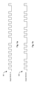
- FIGS. 6 a - 6 c processing changes due to different idle time enforcement processes are graphically shown in timing diagrams 600 , 610 , 620 .
- operation of data detector circuit 330 is shown by shaded regions of a duration 607 .
- operation of data decoding circuit 330 is shown by shaded regions of a duration 609 .
- the operational regions are separated by non-operational regions indicated by a straight line.
- the non-operational regions may represent low level operation such as data loading and unloading, or delay periods.
- the operational regions indicate the ongoing application of a data decode algorithm or a data detection algorithm.
- the next operational period of data detector circuit 330 relies on completion of a previous operational period of data decoding circuit 370
- the next operational period of data decoding circuit 370 relies on completion of a previous operational period of data detection period circuit 330 .
- operation of data detector circuit 330 is shown by combination regions of a duration 615 or a duration 617 .
- the combination regions include a shaded region of a duration 609 that represents the duration of processing required by data detector circuit 330 if the clock is not suppressed, and a non-shaded region that represents the additional duration of processing required because the clock is suppressed.
- the non-shaded region may increase or decrease depending upon the amount of overlap between data decoding circuit 370 and data detection circuit 330 and/or the occurrence of a power usage exceeding a threshold value.
- next operational period of data detector circuit 330 relies on completion of a previous operational period of data decoding circuit 370
- the next operational period of data decoding circuit 370 relies on completion of a previous operational period of data detection period circuit 330 .
- the clock period for data detector circuit 330 is extended (i.e., the processing is delayed) during the period of overlap between data detector circuit 330 and data decoding circuit 370 as shown by periods 680 , 681 , 682 .
- the longer periods 680 , 681 , 682 are, the longer the un-shaded portion of the blocks corresponding to data detector circuit 330 .
- operation of data decoding circuit 370 is shown by combination regions of a duration 627 or a duration 629 .
- the combination regions include a shaded region of a duration 609 that represents the duration of processing required by data decoding circuit 330 if the clock is not suppressed, and a non-shaded region that represents the additional duration of processing required because the clock is suppressed.
- the non-shaded region may increase or decrease depending upon the amount of overlap between data decoding circuit 370 and data detection circuit 330 and/or the occurrence of a power usage exceeding a threshold value.
- the next operational period of data detector circuit 330 relies on completion of a previous operational period of data decoding circuit 370
- the next operational period of data decoding circuit 370 relies on completion of a previous operational period of data detection period circuit 330 .
- Such integrated circuits may include all of the functions of a given block, system or circuit, or a subset of the block, system or circuit. Further, elements of the blocks, systems or circuits may be implemented across multiple integrated circuits. Such integrated circuits may be any type of integrated circuit known in the art including, but are not limited to, a monolithic integrated circuit, a flip chip integrated circuit, a multichip module integrated circuit, and/or a mixed signal integrated circuit. It should also be noted that various functions of the blocks, systems or circuits discussed herein may be implemented in either software or firmware. In some such cases, the entire system, block or circuit may be implemented using its software or firmware equivalent. In other cases, the one part of a given system, block or circuit may be implemented in software or firmware, while other parts are implemented in hardware.
Abstract
Description
| If ( |
| Signal |
| 373 is asserted) |
| { |
| Increment Count of |
| If (Count is equal to N) { |
| If (Mode Select Indicates Suppression of Detector Clock 334) { |
| Suppress current cycle of Detector Clock 334 |
| } |
| Else { |
| Provide |
| } |
| If (Mode Select Indicates Suppression of Decoder Clock 331) { |
| Suppress current cycle of Decoder Clock 331 |
| } |
| Else { |
| Provide |
| } |
| } |
| Else { |
| Provide |
| Provide |
| } |
| } |
| Else { |
| Provide |
| Provide |
| } |
As some examples, N may be equal to four or eight. In some cases, the value of N may be programmable. Based upon the disclosure provided herein, one of ordinary skill in the art will recognize a variety of values that may be used for N.
| If ( |
| |
| |
| { |
| Increment Count of |
| If (Count is equal to N) { |
| If (Mode Select Indicates Suppression of Detector Clock 334) { |
| Suppress current cycle of Detector Clock 334 |
| } |
| Else { |
| Provide |
| } |
| If (Mode Select Indicates Suppression of Decoder Clock 331) { |
| Suppress current cycle of Decoder Clock 331 |
| } |
| Else { |
| Provide |
| } |
| } |
| Else { |
| Provide |
| Provide |
| } |
| } |
| Else { |
| Provide |
| Provide |
| } |
As some examples, N may be equal to four or eight. In some cases, the value of N may be programmable. Based upon the disclosure provided herein, one of ordinary skill in the art will recognize a variety of values that may be used for N.
Claims (22)
Priority Applications (1)
| Application Number | Priority Date | Filing Date | Title |
|---|---|---|---|
| US13/364,217 US8972761B2 (en) | 2012-02-01 | 2012-02-01 | Systems and methods for idle clock insertion based power control |
Applications Claiming Priority (1)
| Application Number | Priority Date | Filing Date | Title |
|---|---|---|---|
| US13/364,217 US8972761B2 (en) | 2012-02-01 | 2012-02-01 | Systems and methods for idle clock insertion based power control |
Publications (2)
| Publication Number | Publication Date |
|---|---|
| US20130198554A1 US20130198554A1 (en) | 2013-08-01 |
| US8972761B2 true US8972761B2 (en) | 2015-03-03 |
Family
ID=48871389
Family Applications (1)
| Application Number | Title | Priority Date | Filing Date |
|---|---|---|---|
| US13/364,217 Active 2033-04-16 US8972761B2 (en) | 2012-02-01 | 2012-02-01 | Systems and methods for idle clock insertion based power control |
Country Status (1)
| Country | Link |
|---|---|
| US (1) | US8972761B2 (en) |
Families Citing this family (2)
| Publication number | Priority date | Publication date | Assignee | Title |
|---|---|---|---|---|
| US10275010B2 (en) * | 2014-02-21 | 2019-04-30 | Mediatek Singapore Pte. Ltd. | Fast and Autonomous mechanism for CPU OC protection |
| CN117312293B (en) * | 2023-11-28 | 2024-04-05 | 福建华电福瑞能源发展有限公司 | Electric power multisource heterogeneous data management and intelligent analysis method and system |
Citations (24)
| Publication number | Priority date | Publication date | Assignee | Title |
|---|---|---|---|---|
| JPH06152288A (en) | 1992-11-06 | 1994-05-31 | Oki Electric Ind Co Ltd | Power controller |
| US5428649A (en) * | 1993-12-16 | 1995-06-27 | International Business Machines Corporation | Elastic buffer with bidirectional phase detector |
| US5544138A (en) | 1993-12-30 | 1996-08-06 | International Business Machines Corporation | Adaptive system for optimizing disk drive power consumption |
| US5715467A (en) | 1996-04-04 | 1998-02-03 | Vlsi Technology, Inc. | Event driven power management control circuit and method therefor |
| US6535056B2 (en) | 2000-06-16 | 2003-03-18 | Hitachi, Ltd. | Semiconductor integrated circuit device |
| JP2003099148A (en) | 2001-09-19 | 2003-04-04 | Sanyo Electric Co Ltd | Data processor and system controller available for the same, and data conversion method |
| WO2004023268A2 (en) | 2002-09-06 | 2004-03-18 | Silicon Image, Inc. | Method and apparatus for double data rate serial ata phy interface |
| JP2004118240A (en) | 2002-09-20 | 2004-04-15 | Ricoh Co Ltd | Network printer system |
| US6748039B1 (en) * | 2000-08-11 | 2004-06-08 | Advanced Micro Devices, Inc. | System and method for synchronizing a skip pattern and initializing a clock forwarding interface in a multiple-clock system |
| US6804792B2 (en) | 2000-02-10 | 2004-10-12 | Kabushiki Kaisha Toshiba | Computer power management with converter for changing generated power mode commands for external devices |
| WO2004109531A2 (en) | 2003-06-10 | 2004-12-16 | Koninklijke Philips Electronics N.V. | Real-time adaptive control for best ic performance |
| US20050144491A1 (en) * | 2003-12-24 | 2005-06-30 | Matsushita Electric Industrial Co., Ltd. | Variable power consumption levels in a hard disk drive |
| US6973583B2 (en) | 2001-09-27 | 2005-12-06 | Oki Electric Industry Co., Ltd. | Information processing apparatus having an interrupt function |
| US6983389B1 (en) | 2002-02-01 | 2006-01-03 | Advanced Micro Devices, Inc. | Clock control of functional units in an integrated circuit based on monitoring unit signals to predict inactivity |
| US7049771B2 (en) | 2004-01-27 | 2006-05-23 | Nippon Yusoki Co., Ltd. | Multi-phase carrier signal generator and multi-phase carrier signal generation method |
| US7055117B2 (en) | 2003-12-29 | 2006-05-30 | Agere Systems, Inc. | System and method for debugging system-on-chips using single or n-cycle stepping |
| US7203857B2 (en) | 2003-03-28 | 2007-04-10 | Elliptic Semiconductor Inc. | On-demand clock switching |
| US7412615B2 (en) | 2003-02-10 | 2008-08-12 | Sony Corporation | Information processing equipment and power consumption control method |
| US7529958B2 (en) | 2004-11-15 | 2009-05-05 | Charles Roth | Programmable power transition counter |
| US7739533B2 (en) | 2006-09-22 | 2010-06-15 | Agere Systems Inc. | Systems and methods for operational power management |
| US20100269074A1 (en) | 2009-04-17 | 2010-10-21 | Lsi Corporation | Predictive Power Management Semiconductor Design Tool and Methods for Using Such |
| US20100268917A1 (en) | 2009-04-17 | 2010-10-21 | Lsi Corporation | Systems and Methods for Ramped Power State Control in a Semiconductor Device |
| US8239700B2 (en) | 2009-04-17 | 2012-08-07 | Lsi Corporation | Systems and methods for power dissipation control in a semiconductor device |
| US8291251B2 (en) | 2006-07-18 | 2012-10-16 | Agere Systems Inc. | Systems and methods for modular power management |
-
2012
- 2012-02-01 US US13/364,217 patent/US8972761B2/en active Active
Patent Citations (25)
| Publication number | Priority date | Publication date | Assignee | Title |
|---|---|---|---|---|
| JPH06152288A (en) | 1992-11-06 | 1994-05-31 | Oki Electric Ind Co Ltd | Power controller |
| US5428649A (en) * | 1993-12-16 | 1995-06-27 | International Business Machines Corporation | Elastic buffer with bidirectional phase detector |
| US5544138A (en) | 1993-12-30 | 1996-08-06 | International Business Machines Corporation | Adaptive system for optimizing disk drive power consumption |
| US5715467A (en) | 1996-04-04 | 1998-02-03 | Vlsi Technology, Inc. | Event driven power management control circuit and method therefor |
| US6804792B2 (en) | 2000-02-10 | 2004-10-12 | Kabushiki Kaisha Toshiba | Computer power management with converter for changing generated power mode commands for external devices |
| US6535056B2 (en) | 2000-06-16 | 2003-03-18 | Hitachi, Ltd. | Semiconductor integrated circuit device |
| US6748039B1 (en) * | 2000-08-11 | 2004-06-08 | Advanced Micro Devices, Inc. | System and method for synchronizing a skip pattern and initializing a clock forwarding interface in a multiple-clock system |
| JP2003099148A (en) | 2001-09-19 | 2003-04-04 | Sanyo Electric Co Ltd | Data processor and system controller available for the same, and data conversion method |
| US6973583B2 (en) | 2001-09-27 | 2005-12-06 | Oki Electric Industry Co., Ltd. | Information processing apparatus having an interrupt function |
| US6983389B1 (en) | 2002-02-01 | 2006-01-03 | Advanced Micro Devices, Inc. | Clock control of functional units in an integrated circuit based on monitoring unit signals to predict inactivity |
| WO2004023268A2 (en) | 2002-09-06 | 2004-03-18 | Silicon Image, Inc. | Method and apparatus for double data rate serial ata phy interface |
| JP2004118240A (en) | 2002-09-20 | 2004-04-15 | Ricoh Co Ltd | Network printer system |
| US7412615B2 (en) | 2003-02-10 | 2008-08-12 | Sony Corporation | Information processing equipment and power consumption control method |
| US7203857B2 (en) | 2003-03-28 | 2007-04-10 | Elliptic Semiconductor Inc. | On-demand clock switching |
| WO2004109531A2 (en) | 2003-06-10 | 2004-12-16 | Koninklijke Philips Electronics N.V. | Real-time adaptive control for best ic performance |
| US20050144491A1 (en) * | 2003-12-24 | 2005-06-30 | Matsushita Electric Industrial Co., Ltd. | Variable power consumption levels in a hard disk drive |
| US7055117B2 (en) | 2003-12-29 | 2006-05-30 | Agere Systems, Inc. | System and method for debugging system-on-chips using single or n-cycle stepping |
| US7049771B2 (en) | 2004-01-27 | 2006-05-23 | Nippon Yusoki Co., Ltd. | Multi-phase carrier signal generator and multi-phase carrier signal generation method |
| US7529958B2 (en) | 2004-11-15 | 2009-05-05 | Charles Roth | Programmable power transition counter |
| US8291251B2 (en) | 2006-07-18 | 2012-10-16 | Agere Systems Inc. | Systems and methods for modular power management |
| US7739533B2 (en) | 2006-09-22 | 2010-06-15 | Agere Systems Inc. | Systems and methods for operational power management |
| US8245061B2 (en) | 2006-09-22 | 2012-08-14 | Agere Systems Inc. | Systems and methods for operational power management utilizing power islands |
| US20100269074A1 (en) | 2009-04-17 | 2010-10-21 | Lsi Corporation | Predictive Power Management Semiconductor Design Tool and Methods for Using Such |
| US20100268917A1 (en) | 2009-04-17 | 2010-10-21 | Lsi Corporation | Systems and Methods for Ramped Power State Control in a Semiconductor Device |
| US8239700B2 (en) | 2009-04-17 | 2012-08-07 | Lsi Corporation | Systems and methods for power dissipation control in a semiconductor device |
Non-Patent Citations (7)
| Title |
|---|
| IBM, "Adaptive Power Management for Mobile Hard Drives", Apr. 1999, see www.almaden.ibm.com/almaden/mobile-hard-drives.html. |
| IBM, "Adaptive Power Management for Mobile Hard Drives", Apr. 1999, see www.almaden.ibm.com/almaden/mobile—hard—drives.html. |
| U.S. Appl. No. 13/167,760, filed Jun. 24, 2011, Changyou Xu, Unpublished. |
| U.S. Appl. No. 13/167,764, filed Jun. 24, 2011, Zongwang Li, Unpublished. |
| U.S. Appl. No. 13/227,557, filed Sep. 8, 2011, Shaohua Yang, Unpublished. |
| U.S. Appl. No. 13/284,684, filed Oct. 28, 2011, Shaohua Yang, Unpublished. |
| U.S. Appl. No. 13/339,403, filed Dec. 29, 2011, Shaohua Yang, Unpublished. |
Also Published As
| Publication number | Publication date |
|---|---|
| US20130198554A1 (en) | 2013-08-01 |
Similar Documents
| Publication | Publication Date | Title |
|---|---|---|
| US8719682B2 (en) | Adaptive calibration of noise predictive finite impulse response filter | |
| US9230596B2 (en) | Systems and methods for variable rate coding in a data processing system | |
| US9043684B2 (en) | Systems and methods for variable redundancy data protection | |
| US20130332794A1 (en) | Data Processing System with Retained Sector Reprocessing | |
| US9190104B2 (en) | Systems and methods for data retry using averaging process | |
| US8731115B2 (en) | Systems and methods for data processing including pre-equalizer noise suppression | |
| US20140313610A1 (en) | Systems and Methods Selective Complexity Data Decoding | |
| US8631300B2 (en) | Systems and methods for scalable data processing shut down | |
| US8972761B2 (en) | Systems and methods for idle clock insertion based power control | |
| US8850289B2 (en) | Quality based priority data processing with soft guaranteed iteration | |
| US8654474B2 (en) | Initialization for decoder-based filter calibration | |
| US20140129905A1 (en) | Flexible Low Density Parity Check Code Seed | |
| US9092368B2 (en) | Systems and methods for modified quality based priority scheduling during iterative data processing | |
| US8749907B2 (en) | Systems and methods for adaptive decoder message scaling | |
| US8817404B1 (en) | Systems and methods for data processing control | |
| US20130275717A1 (en) | Multi-Tier Data Processing | |
| US8839009B2 (en) | Systems and methods for decimation based over-current control | |
| US8917466B1 (en) | Systems and methods for governing in-flight data sets in a data processing system | |
| US8910005B2 (en) | Systems and methods for selective retry data retention processing | |
| US20130205146A1 (en) | Systems and Methods for Power Governance in a Data Processing Circuit | |
| US9324372B2 (en) | Systems and methods for local iteration randomization in a data decoder | |
| US9298369B2 (en) | Modify priority of dataset based on number of times the data set is processed by both a data detector circuit and a data decoder circuit | |
| US8867156B2 (en) | Systems and methods for P-distance based priority data processing | |
| US8976471B1 (en) | Systems and methods for two stage tone reduction | |
| US20130219233A1 (en) | Systems and Methods for Quality Based Priority Data Processing |
Legal Events
| Date | Code | Title | Description |
|---|---|---|---|
| AS | Assignment |
Owner name: LSI CORPORATION, CALIFORNIA Free format text: ASSIGNMENT OF ASSIGNORS INTEREST;ASSIGNORS:YANG, SHAOHUA;XU, CHANGYOU;ZHANG, FAN;SIGNING DATES FROM 20120127 TO 20120201;REEL/FRAME:027636/0703 |
|
| AS | Assignment |
Owner name: DEUTSCHE BANK AG NEW YORK BRANCH, AS COLLATERAL AG Free format text: PATENT SECURITY AGREEMENT;ASSIGNORS:LSI CORPORATION;AGERE SYSTEMS LLC;REEL/FRAME:032856/0031 Effective date: 20140506 |
|
| STCF | Information on status: patent grant |
Free format text: PATENTED CASE |
|
| AS | Assignment |
Owner name: AVAGO TECHNOLOGIES GENERAL IP (SINGAPORE) PTE. LTD Free format text: ASSIGNMENT OF ASSIGNORS INTEREST;ASSIGNOR:LSI CORPORATION;REEL/FRAME:035390/0388 Effective date: 20140814 |
|
| AS | Assignment |
Owner name: LSI CORPORATION, CALIFORNIA Free format text: TERMINATION AND RELEASE OF SECURITY INTEREST IN PATENT RIGHTS (RELEASES RF 032856-0031);ASSIGNOR:DEUTSCHE BANK AG NEW YORK BRANCH, AS COLLATERAL AGENT;REEL/FRAME:037684/0039 Effective date: 20160201 Owner name: AGERE SYSTEMS LLC, PENNSYLVANIA Free format text: TERMINATION AND RELEASE OF SECURITY INTEREST IN PATENT RIGHTS (RELEASES RF 032856-0031);ASSIGNOR:DEUTSCHE BANK AG NEW YORK BRANCH, AS COLLATERAL AGENT;REEL/FRAME:037684/0039 Effective date: 20160201 |
|
| AS | Assignment |
Owner name: BANK OF AMERICA, N.A., AS COLLATERAL AGENT, NORTH CAROLINA Free format text: PATENT SECURITY AGREEMENT;ASSIGNOR:AVAGO TECHNOLOGIES GENERAL IP (SINGAPORE) PTE. LTD.;REEL/FRAME:037808/0001 Effective date: 20160201 Owner name: BANK OF AMERICA, N.A., AS COLLATERAL AGENT, NORTH Free format text: PATENT SECURITY AGREEMENT;ASSIGNOR:AVAGO TECHNOLOGIES GENERAL IP (SINGAPORE) PTE. LTD.;REEL/FRAME:037808/0001 Effective date: 20160201 |
|
| AS | Assignment |
Owner name: AVAGO TECHNOLOGIES GENERAL IP (SINGAPORE) PTE. LTD., SINGAPORE Free format text: TERMINATION AND RELEASE OF SECURITY INTEREST IN PATENTS;ASSIGNOR:BANK OF AMERICA, N.A., AS COLLATERAL AGENT;REEL/FRAME:041710/0001 Effective date: 20170119 Owner name: AVAGO TECHNOLOGIES GENERAL IP (SINGAPORE) PTE. LTD Free format text: TERMINATION AND RELEASE OF SECURITY INTEREST IN PATENTS;ASSIGNOR:BANK OF AMERICA, N.A., AS COLLATERAL AGENT;REEL/FRAME:041710/0001 Effective date: 20170119 |
|
| MAFP | Maintenance fee payment |
Free format text: PAYMENT OF MAINTENANCE FEE, 4TH YEAR, LARGE ENTITY (ORIGINAL EVENT CODE: M1551); ENTITY STATUS OF PATENT OWNER: LARGE ENTITY Year of fee payment: 4 |
|
| AS | Assignment |
Owner name: AVAGO TECHNOLOGIES INTERNATIONAL SALES PTE. LIMITE Free format text: MERGER;ASSIGNOR:AVAGO TECHNOLOGIES GENERAL IP (SINGAPORE) PTE. LTD.;REEL/FRAME:047422/0464 Effective date: 20180509 |
|
| AS | Assignment |
Owner name: AVAGO TECHNOLOGIES INTERNATIONAL SALES PTE. LIMITE Free format text: CORRECTIVE ASSIGNMENT TO CORRECT THE EXECUTION DATE PREVIOUSLY RECORDED AT REEL: 047422 FRAME: 0464. ASSIGNOR(S) HEREBY CONFIRMS THE MERGER;ASSIGNOR:AVAGO TECHNOLOGIES GENERAL IP (SINGAPORE) PTE. LTD.;REEL/FRAME:048883/0702 Effective date: 20180905 |
|
| AS | Assignment |
Owner name: BROADCOM INTERNATIONAL PTE. LTD., SINGAPORE Free format text: ASSIGNMENT OF ASSIGNORS INTEREST;ASSIGNOR:AVAGO TECHNOLOGIES INTERNATIONAL SALES PTE. LIMITED;REEL/FRAME:053771/0901 Effective date: 20200826 |
|
| MAFP | Maintenance fee payment |
Free format text: PAYMENT OF MAINTENANCE FEE, 8TH YEAR, LARGE ENTITY (ORIGINAL EVENT CODE: M1552); ENTITY STATUS OF PATENT OWNER: LARGE ENTITY Year of fee payment: 8 |
|
| AS | Assignment |
Owner name: AVAGO TECHNOLOGIES INTERNATIONAL SALES PTE. LIMITED, SINGAPORE Free format text: MERGER;ASSIGNORS:AVAGO TECHNOLOGIES INTERNATIONAL SALES PTE. LIMITED;BROADCOM INTERNATIONAL PTE. LTD.;REEL/FRAME:062952/0850 Effective date: 20230202 |