US8975615B2 - Method of fabricating optical devices using laser treatment of contact regions of gallium and nitrogen containing material - Google Patents
Method of fabricating optical devices using laser treatment of contact regions of gallium and nitrogen containing material Download PDFInfo
- Publication number
- US8975615B2 US8975615B2 US13/291,922 US201113291922A US8975615B2 US 8975615 B2 US8975615 B2 US 8975615B2 US 201113291922 A US201113291922 A US 201113291922A US 8975615 B2 US8975615 B2 US 8975615B2
- Authority
- US
- United States
- Prior art keywords
- region
- laser
- scribe
- gallium
- contact
- Prior art date
- Legal status (The legal status is an assumption and is not a legal conclusion. Google has not performed a legal analysis and makes no representation as to the accuracy of the status listed.)
- Active
Links
Images


Classifications
-
- H—ELECTRICITY
- H01—ELECTRIC ELEMENTS
- H01L—SEMICONDUCTOR DEVICES NOT COVERED BY CLASS H10
- H01L33/00—Semiconductor devices with at least one potential-jump barrier or surface barrier specially adapted for light emission; Processes or apparatus specially adapted for the manufacture or treatment thereof or of parts thereof; Details thereof
- H01L33/02—Semiconductor devices with at least one potential-jump barrier or surface barrier specially adapted for light emission; Processes or apparatus specially adapted for the manufacture or treatment thereof or of parts thereof; Details thereof characterised by the semiconductor bodies
- H01L33/20—Semiconductor devices with at least one potential-jump barrier or surface barrier specially adapted for light emission; Processes or apparatus specially adapted for the manufacture or treatment thereof or of parts thereof; Details thereof characterised by the semiconductor bodies with a particular shape, e.g. curved or truncated substrate
-
- B—PERFORMING OPERATIONS; TRANSPORTING
- B82—NANOTECHNOLOGY
- B82Y—SPECIFIC USES OR APPLICATIONS OF NANOSTRUCTURES; MEASUREMENT OR ANALYSIS OF NANOSTRUCTURES; MANUFACTURE OR TREATMENT OF NANOSTRUCTURES
- B82Y20/00—Nanooptics, e.g. quantum optics or photonic crystals
-
- H—ELECTRICITY
- H01—ELECTRIC ELEMENTS
- H01S—DEVICES USING THE PROCESS OF LIGHT AMPLIFICATION BY STIMULATED EMISSION OF RADIATION [LASER] TO AMPLIFY OR GENERATE LIGHT; DEVICES USING STIMULATED EMISSION OF ELECTROMAGNETIC RADIATION IN WAVE RANGES OTHER THAN OPTICAL
- H01S5/00—Semiconductor lasers
- H01S5/04—Processes or apparatus for excitation, e.g. pumping, e.g. by electron beams
- H01S5/042—Electrical excitation ; Circuits therefor
- H01S5/0425—Electrodes, e.g. characterised by the structure
- H01S5/04254—Electrodes, e.g. characterised by the structure characterised by the shape
-
- H—ELECTRICITY
- H01—ELECTRIC ELEMENTS
- H01S—DEVICES USING THE PROCESS OF LIGHT AMPLIFICATION BY STIMULATED EMISSION OF RADIATION [LASER] TO AMPLIFY OR GENERATE LIGHT; DEVICES USING STIMULATED EMISSION OF ELECTROMAGNETIC RADIATION IN WAVE RANGES OTHER THAN OPTICAL
- H01S5/00—Semiconductor lasers
- H01S5/20—Structure or shape of the semiconductor body to guide the optical wave ; Confining structures perpendicular to the optical axis, e.g. index or gain guiding, stripe geometry, broad area lasers, gain tailoring, transverse or lateral reflectors, special cladding structures, MQW barrier reflection layers
- H01S5/22—Structure or shape of the semiconductor body to guide the optical wave ; Confining structures perpendicular to the optical axis, e.g. index or gain guiding, stripe geometry, broad area lasers, gain tailoring, transverse or lateral reflectors, special cladding structures, MQW barrier reflection layers having a ridge or stripe structure
- H01S5/2201—Structure or shape of the semiconductor body to guide the optical wave ; Confining structures perpendicular to the optical axis, e.g. index or gain guiding, stripe geometry, broad area lasers, gain tailoring, transverse or lateral reflectors, special cladding structures, MQW barrier reflection layers having a ridge or stripe structure in a specific crystallographic orientation
-
- H—ELECTRICITY
- H01—ELECTRIC ELEMENTS
- H01S—DEVICES USING THE PROCESS OF LIGHT AMPLIFICATION BY STIMULATED EMISSION OF RADIATION [LASER] TO AMPLIFY OR GENERATE LIGHT; DEVICES USING STIMULATED EMISSION OF ELECTROMAGNETIC RADIATION IN WAVE RANGES OTHER THAN OPTICAL
- H01S5/00—Semiconductor lasers
- H01S5/30—Structure or shape of the active region; Materials used for the active region
- H01S5/32—Structure or shape of the active region; Materials used for the active region comprising PN junctions, e.g. hetero- or double- heterostructures
- H01S5/3202—Structure or shape of the active region; Materials used for the active region comprising PN junctions, e.g. hetero- or double- heterostructures grown on specifically orientated substrates, or using orientation dependent growth
- H01S5/32025—Structure or shape of the active region; Materials used for the active region comprising PN junctions, e.g. hetero- or double- heterostructures grown on specifically orientated substrates, or using orientation dependent growth non-polar orientation
-
- H—ELECTRICITY
- H01—ELECTRIC ELEMENTS
- H01L—SEMICONDUCTOR DEVICES NOT COVERED BY CLASS H10
- H01L2924/00—Indexing scheme for arrangements or methods for connecting or disconnecting semiconductor or solid-state bodies as covered by H01L24/00
-
- H—ELECTRICITY
- H01—ELECTRIC ELEMENTS
- H01L—SEMICONDUCTOR DEVICES NOT COVERED BY CLASS H10
- H01L2924/00—Indexing scheme for arrangements or methods for connecting or disconnecting semiconductor or solid-state bodies as covered by H01L24/00
- H01L2924/0001—Technical content checked by a classifier
- H01L2924/0002—Not covered by any one of groups H01L24/00, H01L24/00 and H01L2224/00
-
- H—ELECTRICITY
- H01—ELECTRIC ELEMENTS
- H01L—SEMICONDUCTOR DEVICES NOT COVERED BY CLASS H10
- H01L33/00—Semiconductor devices with at least one potential-jump barrier or surface barrier specially adapted for light emission; Processes or apparatus specially adapted for the manufacture or treatment thereof or of parts thereof; Details thereof
- H01L33/005—Processes
- H01L33/0095—Post-treatment of devices, e.g. annealing, recrystallisation or short-circuit elimination
-
- H—ELECTRICITY
- H01—ELECTRIC ELEMENTS
- H01S—DEVICES USING THE PROCESS OF LIGHT AMPLIFICATION BY STIMULATED EMISSION OF RADIATION [LASER] TO AMPLIFY OR GENERATE LIGHT; DEVICES USING STIMULATED EMISSION OF ELECTROMAGNETIC RADIATION IN WAVE RANGES OTHER THAN OPTICAL
- H01S2304/00—Special growth methods for semiconductor lasers
- H01S2304/04—MOCVD or MOVPE
-
- H—ELECTRICITY
- H01—ELECTRIC ELEMENTS
- H01S—DEVICES USING THE PROCESS OF LIGHT AMPLIFICATION BY STIMULATED EMISSION OF RADIATION [LASER] TO AMPLIFY OR GENERATE LIGHT; DEVICES USING STIMULATED EMISSION OF ELECTROMAGNETIC RADIATION IN WAVE RANGES OTHER THAN OPTICAL
- H01S5/00—Semiconductor lasers
- H01S5/02—Structural details or components not essential to laser action
- H01S5/0201—Separation of the wafer into individual elements, e.g. by dicing, cleaving, etching or directly during growth
- H01S5/0202—Cleaving
-
- H—ELECTRICITY
- H01—ELECTRIC ELEMENTS
- H01S—DEVICES USING THE PROCESS OF LIGHT AMPLIFICATION BY STIMULATED EMISSION OF RADIATION [LASER] TO AMPLIFY OR GENERATE LIGHT; DEVICES USING STIMULATED EMISSION OF ELECTROMAGNETIC RADIATION IN WAVE RANGES OTHER THAN OPTICAL
- H01S5/00—Semiconductor lasers
- H01S5/02—Structural details or components not essential to laser action
- H01S5/0206—Substrates, e.g. growth, shape, material, removal or bonding
- H01S5/0217—Removal of the substrate
-
- H—ELECTRICITY
- H01—ELECTRIC ELEMENTS
- H01S—DEVICES USING THE PROCESS OF LIGHT AMPLIFICATION BY STIMULATED EMISSION OF RADIATION [LASER] TO AMPLIFY OR GENERATE LIGHT; DEVICES USING STIMULATED EMISSION OF ELECTROMAGNETIC RADIATION IN WAVE RANGES OTHER THAN OPTICAL
- H01S5/00—Semiconductor lasers
- H01S5/02—Structural details or components not essential to laser action
- H01S5/028—Coatings ; Treatment of the laser facets, e.g. etching, passivation layers or reflecting layers
-
- H—ELECTRICITY
- H01—ELECTRIC ELEMENTS
- H01S—DEVICES USING THE PROCESS OF LIGHT AMPLIFICATION BY STIMULATED EMISSION OF RADIATION [LASER] TO AMPLIFY OR GENERATE LIGHT; DEVICES USING STIMULATED EMISSION OF ELECTROMAGNETIC RADIATION IN WAVE RANGES OTHER THAN OPTICAL
- H01S5/00—Semiconductor lasers
- H01S5/30—Structure or shape of the active region; Materials used for the active region
- H01S5/34—Structure or shape of the active region; Materials used for the active region comprising quantum well or superlattice structures, e.g. single quantum well [SQW] lasers, multiple quantum well [MQW] lasers or graded index separate confinement heterostructure [GRINSCH] lasers
- H01S5/343—Structure or shape of the active region; Materials used for the active region comprising quantum well or superlattice structures, e.g. single quantum well [SQW] lasers, multiple quantum well [MQW] lasers or graded index separate confinement heterostructure [GRINSCH] lasers in AIIIBV compounds, e.g. AlGaAs-laser, InP-based laser
- H01S5/34333—Structure or shape of the active region; Materials used for the active region comprising quantum well or superlattice structures, e.g. single quantum well [SQW] lasers, multiple quantum well [MQW] lasers or graded index separate confinement heterostructure [GRINSCH] lasers in AIIIBV compounds, e.g. AlGaAs-laser, InP-based laser with a well layer based on Ga(In)N or Ga(In)P, e.g. blue laser
Definitions
- the invention is directed to optical devices and related methods.
- the invention provides a method and device for emitting electromagnetic radiation using nonpolar gallium containing substrates such as GaN, MN, InN, InGaN, AlGaN, and AlInGaN, and others.
- the present method and device uses a laser scribing process to ablate a portion of a contact region for improved device performance.
- the invention can be applied to optical devices, lasers, light emitting diodes, solar cells, photoelectrochemical water splitting and hydrogen generation, photodetectors, integrated circuits, and transistors, among other devices.
- the Ar-ion laser utilized a noble gas as the active medium and produce laser light output in the UV, blue, and green wavelengths including 351 nm, 454.6 nm, 457.9 nm, 465.8 nm, 476.5 nm, 488.0 nm, 496.5 nm, 501.7 nm, 514.5 nm, and 528.7 nm.
- the Ar-ion laser had the benefit of producing highly directional and focusable light with a narrow spectral output, but the efficiency, size, weight, and cost of the lasers were undesirable.
- lamp pumped solid state lasers were developed in the infrared, and the output wavelength was converted to the visible using specialty crystals with nonlinear optical properties.
- a green lamp pumped solid state lasers had 3 stages: electricity powers lamp, lamp excites gain crystal which lases at 1064 nm, 1064 nm goes into frequency conversion crystal which converts to visible 532 nm.
- the resulting green and blue lasers were called “lamped pumped solid state lasers with second harmonic generation” (LPSS with SHG) and were more efficient than Ar-ion gas lasers, but were still too inefficient, large, expensive, fragile for broad deployment outside of specialty scientific and medical applications. Additionally, the gain crystal used in the solid state lasers typically had energy storage properties which made the lasers difficult to modulate at high speeds which limited its broader deployment.
- DPSS with SHG “diode pumped solid state lasers with SHG”
- the DPSS laser technology extended the life and improved the efficiency of the LPSS lasers, and further commercialization ensue into more high end specialty industrial, medical, and scientific applications.
- the change to diode pumping increased the system cost and required precised temperature controls, leaving the laser with substantial size, power consumption while not addressing the energy storage properties which made the lasers difficult to modulate at high speeds.
- the invention provides a method and device for emitting electromagnetic radiation using nonpolar gallium containing substrates such as GaN, MN, InN, InGaN, AlGaN, and AlInGaN, and others. More particularly, the present method and device uses a laser scribing process to ablate a portion of a contact region for improved device performance.
- the electromagnetic radiation has a wavelength of 395, 405, 450, 485, 500, 520, nanometers and others.
- the invention can be applied to optical devices, lasers, light emitting diodes, solar cells, photoelectrochemical water splitting and hydrogen generation, photodetectors, integrated circuits, and transistors.
- the invention provides a method for forming optical devices.
- the method includes providing a gallium and nitrogen containing substrate member having a first surface region and a second surface region, and which has a contact region.
- the gallium and nitrogen containing substrate member includes at least one optical device.
- the method includes subjecting the contact region in a portion of the substrate to a laser scribing process to form a scribe region causing a gallium rich region within a vicinity of the scribe region; while maintaining a desired thermal budget within the optical device.
- the invention provides an optical device, e.g., laser or LED.
- the device includes a gallium nitride substrate having a crystalline surface region and a backside region.
- the surface region is configured with a non-polar or semipolar orientation.
- the device has a scribe line on the backside configured from a laser process.
- a metallization material overlies the backside and the scribe line. The scribe region formed on a contact region improves device performance.
- the invention also provides a method for forming optical devices.
- the method includes providing a gallium nitride substrate member having a crystalline surface region and a backside.
- the method includes subjecting the backside to a laser scribing process to form scribe regions on the backside and then forming a metallization material over the backside and the scribe regions.
- the scribe process is followed by a break process to remove and separate the optical device from a remaining portion of the substrate member.
- the laser scribing process may be performed after forming metallization material overlying the backside.
- the scribe region provides improved device performance by ablating portions of the gallium and nitrogen material in the contact region.
- the method also includes forming active regions configured to emit electromagnetic radiation for an optical device.
- the method forms a metallization material overlying a surface region, e.g., backside, frontside, edges, or combinations.
- the method includes subjecting the surface region to a laser treatment process to change the operating voltage of the optical device from a first value to a reduced second value.
- the method includes formation of a scribe region on the surface region, and then removing the optical device using the scribe region.
- the laser scribing process forms a scribe region which also causes a gallium rich region around the scribe region, yet maintains a thermal budget within the optical devices. It is believed that forming the scribe region in this manner causes nucleated gallium metal material to be formed around the scribe region.
- the invention enables a cost-effective optical device for laser applications.
- the optical device can be manufactured in a relatively simple and cost effective manner.
- the apparatus and method can be manufactured using conventional materials and/or methods.
- the laser device uses a nonpolar gallium nitride material to achieve a laser having a wavelength of about 400 nanometers and greater.
- the resulting laser or light emitting diode device has an improved contact, which is lower in resistance and provides a lower voltage drop through the device.
- the improved contacts use a combination of localized, high temperature annealing of the contact and intermixing between the contact metal and the gallium and nitrogen containing substrate.
- FIG. 1 is a perspective view of a laser device fabricated on a nonpolar substrate
- FIG. 2 is a cross-sectional view of a laser device fabricated on a nonpolar substrate
- FIG. 3 is a cross-sectional view photograph of an c-direction cleaved facet for a laser device
- FIG. 4 is a top-view diagram of a laser device
- FIG. 4A is a cross-sectional view diagram of a scribe region for a laser device
- FIG. 4B is a cross-sectional view diagram of a scribe region for a LED device
- FIG. 4C is a top-view diagram of scribe regions for laser devices
- FIG. 4D is a top-view diagram of various contact regions including scribe region patterns
- FIG. 4E is a top-view diagram of scribed contact regions
- FIGS. 5 to 12 illustrate a backend processing method of a laser device
- FIGS. 13 to 18 illustrate a laser scribe process for improving contact regions of an optical device
- FIGS. 19 and 20 are diagram illustrating experimental results of a laser scribing process for contact formation
- FIG. 21 are images of scribe regions for laser devices
- FIG. 22 is an image of scribe regions configured in a ladder pattern
- FIG. 23 is an image of scribe regions configured in a ladder pattern
- FIG. 24 is a contact IV curve (1) with a scribe region; (2) without a scribe region; and
- FIGS. 25 and 26 illustrate experimental results of multiple scribe regions.
- FIG. 1 is a perspective view of a laser device 100 fabricated on a non-polar substrate.
- the optical device includes a gallium nitride substrate 101 having a nonpolar crystalline surface region characterized by an orientation of about ⁇ 6 degrees to about 6 degrees towards (000-1) and less than about 0.5 degrees towards (11-20).
- the gallium nitride substrate is a bulk GaN substrate characterized by a nonpolar crystalline surface region.
- the bulk nitride GaN substrate comprises nitrogen and has a surface dislocation density below 10 5 cm ⁇ 2 .
- the nitride crystal or wafer may comprise Al x In y Ga 1-x-y N, where 0 ⁇ x, y, x+y ⁇ 1.
- the nitride crystal comprises GaN which has threading dislocations,at a concentration between about 10 5 cm ⁇ 2 and about 10 8 cm ⁇ 2 , in a direction that is substantially orthogonal or oblique with respect to the surface.
- the surface dislocation density is below about 10 5 cm ⁇ 2 .
- the device has a laser stripe region formed overlying a portion of the nonpolar crystalline orientation surface region.
- the laser stripe region is characterized by a cavity orientation is substantially parallel to the c-direction, and has a first end 107 and a second end 109 .
- the device has a first cleaved c-face facet provided on the first end of the laser stripe region and a second cleaved c-face facet provided on the second end of the laser stripe region.
- the first cleaved c-facet is substantially parallel with the second cleaved c-facet.
- Mirror surfaces are formed on each of the cleaved surfaces.
- the first cleaved c-facet provides a first mirror surface, e.g. by a scribing and breaking process.
- the scribing process can use any suitable techniques, such as a diamond scribe or laser scribe.
- the reflective coating is selected from silicon dioxide, hafnia, and titaniatantalum pentoxidezirconia, or combinations thereof, and the like.
- the first mirror surface can also comprise an anti-reflective coating.
- the second cleaved c-facet provides a second mirror surface, e.g. using the same techniques.
- the laser stripe has a length from about 50 microns to about 3000 microns.
- the strip has a width ranging from about 0.5 microns to about 50 microns.
- the width is substantially constant in dimension, although there may be slight variations. The width and length are often formed using a masking and etching process, as commonly used in the art.
- the device is also characterized by a spontaneously emitted light polarized in substantially perpendicular to the c-direction, e.g. the device performs as a laser.
- the light is characterized by a polarization ratio of greater than 0.1 to about 1 perpendicular to the c-direction, and a wavelength of about 405 nanometers.
- the spontaneously emitted light is highly polarized and is characterized by a polarization ratio of greater than 0.4.
- FIG. 2 is a cross-sectional view of a laser device 200 fabricated on a nonpolar substrate according to an embodiment of the invention.
- the laser device includes a gallium nitride substrate 203 , which has an underlying n-type metal back contact region 201 .
- the metal back contact region is made of a suitable material such as those noted below.
- the device also has an overlying n-type gallium nitride layer 205 , an active region 207 , and an overlying p-type gallium nitride layer structured as a laser stripe region 209 .
- Each of these regions can be formed using an epitaxial deposition technique of metal organic chemical vapor deposition (MOCVD), molecular beam epitaxy (MBE), or other epitaxial growth techniques suitable for GaN growth.
- MOCVD metal organic chemical vapor deposition
- MBE molecular beam epitaxy
- the epitaxial layer is a high quality epitaxial layer overlying the n-type gallium nitride layer.
- the high quality layer is doped, for example, with Si or O to form n-type material, with a dopant concentration between about 10 16 cm ⁇ 3 and 10 20 cm ⁇ 3 .
- the carrier concentration is preferably in the range between about 10 16 cm ⁇ 3 and 10 20 cm ⁇ 3 .
- the deposition may be performed using metalorganic chemical vapor deposition (MOCVD) or molecular beam epitaxy (MBE).
- the bulk GaN substrate is placed on a susceptor in an MOCVD reactor.
- the susceptor is heated to a temperature between about 1000 and about 1200 degrees Celsius in the presence of a nitrogen-containing gas.
- the susceptor is heated to approximately 1100 degrees Celsius under flowing ammonia.
- a flow of a gallium-containing metalorganic precursor, such as trimethylgallium (TMG) or triethylgallium (TEG) is initiated, in a carrier gas, at a total rate between approximately 1 and 50 standard cubic centimeters per minute (sccm).
- the carrier gas may comprise hydrogen, helium, nitrogen, or argon.
- the ratio of the flow rate of the group V precursor (ammonia) to that of the group III precursor (trimethylgallium, triethylgallium, trimethylindium, trimethylaluminum) during growth is between about 2000 to 12000.
- a flow of disilane in a carrier gas, with a total flow rate of between about 0.1 and 10 sccm is initiated.
- the laser stripe region is made of the p-type gallium nitride layer 209 which is defined by an etching process, for example, a dry etching process using an inductively coupled process with chlorine bearing species or a reactive ion etching process using similar chemistries.
- the chlorine bearing species are commonly derived from chlorine gas or the like.
- the device also has an overlying dielectric region, which exposes 213 contact region.
- the dielectric region is an oxide such as silicon dioxide or silicon nitride.
- the contact region is coupled to an overlying metal layer 215 which can be a multilayered structure, e.g. containing gold and platinum (Pt/Au).
- the laser device has active region 207 which can include, e.g. 1 to 20 quantum well regions.
- active region 207 can include, e.g. 1 to 20 quantum well regions.
- an active layer is deposited.
- the active layer may provide a single quantum well or multiple quantum wells.
- the quantum wells may comprise InGaN wells and GaN barrier layers.
- the well layers and barrier layers comprise Al w In x Ga 1-w-x N and Al y In z Ga 1-y-z N, respectively, where 0 ⁇ w, x, y, z, w+x, y+z ⁇ 1, where w ⁇ u, y and/or x>v, z so that the bandgap of the well layer(s) is less than that of the barrier layer(s) and the n-type layer.
- the well layers and barrier layers may each have a thickness between about 1 nm and about 40 nm.
- the active layer comprises a double heterostructure, with an InGaN or Al w In x Ga 1-w-x N layer about 10 nm to 100 nm thick surrounded by GaN or Al y In z Ga 1-y-z N layers, where w ⁇ u, y and/or x>v, z.
- the composition and structure of the active layer are chosen to provide light emission at a preselected wavelength.
- the active layer may be left undoped (or unintentionally doped) or may be doped n-type or p-type.
- the active region can also include an electron blocking region, and a separate confinement heterostructure.
- an electron blocking layer is preferably deposited.
- the electron-blocking layer may comprise Al s In t Ga 1-s-t N, where 0 ⁇ s, t, s+t ⁇ 1, with a higher bandgap than the active layer, and may be doped p-type.
- the electron blocking layer comprises AlGaN.
- the electron blocking layer comprises an AlGaN/GaN super-lattice structure, with alternating layers of AlGaN and GaN, each with a thickness between about 0.2 nm and about 5 nm.
- the p-type gallium nitride structure which can be a p-type doped AlqInrGa 1-q-r N, where 0 ⁇ q, r, q+r ⁇ 1, layer is deposited above the active layer.
- the p-type layer may be doped with Mg, to a level between about 10 16 cm ⁇ 3 and 10 22 cm ⁇ 3 , and may have a thickness between about 5 nm and about 1000 nm.
- the outermost 1-50 nm of the p-type layer is doped more heavily than the rest of the layer to enable an improved electrical contact.
- the laser stripe is provided by an etching process.
- the device also has an overlying dielectric region, e.g. silicon dioxide to expose a contact region. In a specific embodiment, the dielectric region is an oxide such as silicon dioxide.
- the metal contact is made of suitable material, e.g. silver, gold, aluminum, nickel, platinum, rhodium, palladium, chromium, or the like.
- the electrical contact may be deposited by thermal evaporation, electron beam evaporation, electroplating, sputtering, or another suitable technique.
- the electrical contact serves as a p-type or n-type electrode for the optical device.
- FIG. 3 is a cross-sectional view photograph of a c-direction cleaved facet for a laser device. As shown, the c-direction cleaved facet is smooth and provides a suitable mirror surface. Details of the top-view of the laser device are provided below.
- FIG. 4 is a top-view diagram of a laser device. As shown, the laser stripe is configured in the c-direction, which has a projection normal to the c-direction.
- the top-view of the gallium nitride substrate is of a slight mis-cut or off-cut surface region orientation.
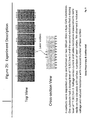
- FIG. 4A is a cross-sectional view diagram of a scribe region for a laser device.
- the laser device includes a gallium and nitrogen containing substrate having a backside region, which is configured with a scribe region, which is a v-shaped or trench shaped cut.
- the scribe region includes a gallium rich gallium nitride region (as shown by the dotted lines), which has a greater amount of gallium than the conventional stoichiometry of gallium nitride.
- the gallium rich region has higher carrier concentration than gallium nitride.
- the device also includes overlying metallization, which can be, e.g.
- the metallization is substantially free from damage and has been formed after the laser scribing process.
- the scribe region is formed on an n-type contact, which is a nitrogen face for c-plane. In other embodiments, the scribe region may be formed on other planes, e.g, semipolar, non-polar.
- the nitrogen face is often more difficult for an ohmic-contact.
- the process forms an ohmic-contact, which is substantially Schottky free in characteristic.
- metal nucleation (not shown) also forms within a vicinity of the scribe region, but is later removed.
- Laser devices are formed on the face opposite of the metallization, and are substantially free from damage by way of localized heating from the laser process.
- FIG. 4B is a cross-sectional view diagram of a scribe region for a LED device.
- the present LED device includes a gallium and nitrogen containing substrate.
- the substrate includes a backside region, which is configured with a v-shaped or trench shaped cut.
- the scribe region has been provided by a laser scribe process further described below.
- the scribe region includes a gallium rich gallium nitride region (as shown in the dotted lines), which has a greater amount of gallium than the conventional stoichiometry of gallium nitride.
- the gallium rich region has higher carrier concentration than gallium nitride.
- the device also includes an overlying metallization, which can be an aluminum, nickel, gold stack, a titanium nickel gold stack, a titanium gold stack, a platinum material, or a silicon, aluminum, nickel, gold stack, or other material.
- an overlying metallization which can be an aluminum, nickel, gold stack, a titanium nickel gold stack, a titanium gold stack, a platinum material, or a silicon, aluminum, nickel, gold stack, or other material.
- the metallization has been damaged from the laser process and portions of the metallization form an alloy with the gallium and nitrogen containing material.
- the scribe region is preferably formed on an n-type contact, which is a nitrogen face for c-plane. In other embodiments, the scribe region may be formed on other planes, e.g, semipolar, non-polar. The nitrogen face is often more difficult form an ohmic-contact.
- the invention forms an ohmic-contact, which is substantially Schottky free in characteristic.
- LED devices are formed on the face opposite of the metallization. The LED devices are substantially free from damage by way of localized heating from the LED process.
- FIG. 4C is a top-view diagram of scribe regions for laser devices.
- the top-view is representative of a backside of a laser device.
- the backside of the laser device can be for an n-contact region, and others.
- the n-contact region can be a nitrogen face for c-plane, but can be other plans, e.g., semipolar, non-polar.
- the laser scribes are formed in a parallel arrangement from a first region to a second region of the backside.
- the laser scribes are provide within regions of the contacts and are not used for breaking purposes. Scribing contact regions improves carrier concentration and device performance.
- the substrate includes a plurality of laser devices.
- FIG. 4D is a top-view diagram of various contact regions including scribe region patterns. As shown, various contact regions are illustrated by respective annular regions, e.g., circular in shape. Each of the annular regions is configured with laser scribe patterns having a width, a shape, a depth, and a length. Depending upon the embodiment, multiple patterns can be used.
- a single scribe line As shown include (from left to right and then top to bottom) a single scribe line, multiple scribe lines in parallel to each other and separated by a gap of about a width of the scribe line, multiple scribe lines in parallel to each other and separated by a larger gap than a width of the scribe line, three scribe lines in parallel to each other, four scribe lines in parallel to each other, two scribe lines in a cross formation, four scribe lines in a box formation, a smaller single scribe line, and a longer single scribe line configured across a diameter of the contact region.
- the present method and device includes multiple scribe lines, which are separated by at least a width of the scribe line. In a more preferred embodiment, a higher number of scribes is preferred over a lower number. In an additional preferred embodiment, the scribe patterns are configured in a box like manner. These scribe patterns achieve improved contact performance leading to improved device performance.
- FIG. 4E is a top-view diagram of scribed contact regions.
- the gallium and nitrogen containing substrate includes a plurality of annular contact regions.
- Each of the contact regions corresponds to at least one optical device, e.g., LED.
- the contact regions are formed on a backside of the substrate, which is an n-type contact region. Ohmic contacts are achieved on each of the n-type contact regions.
- the scribe region penetrates into a portion of the gallium and nitrogen containing substrate, and through a portion of the metallization, which may be formed before or after the scribe region. Again, the scribe region is not for separating the optical device.
- the above sequence of steps is used to form individual laser devices on a die from a substrate structure.
- the method includes cleaved facets substantially parallel to each other and facing each other in a ridge laser device configured on a non-polar gallium nitride substrate material.
- the above sequence of steps is used to form individual LED devices on a die from a substrate structure.
- the method includes scribing before or after n-contact pad definition.
- FIG. 6 is a illustrating of a substrate thinning process according to an embodiment of the invention.
- the method begins with a gallium nitride substrate material including laser devices and preferably ridge laser devices.
- the substrate has been subjected to front side processing.
- front side processing After front side processing has been completed, one or more of the GaN substrates are mounted front side down onto a sapphire carrier wafer or other suitable member.
- the method uses Crystalbond 509, a conventional mounting thermoplastic.
- the thermoplastic can be dissolved in acetone or other suitable solvent.
- the carrier wafer is mounted to a lapping jig.
- lapping jig An example of such lapping jig is made by Logitech Ltd. (Logitech) of the United Kingdom, or other vendor.
- the lapping jig helps maintain planarity of the substrates during the lapping process.
- the starting thickness of the substrates are ⁇ 325 um+/ ⁇ 20 um.
- the method laps or thins the substrates down to 70-80 um thickness.
- the lapping jig is configured with a lapping plate, which is often made of a suitable material such as cast iron configured with a flatness of less than 5 um.
- the method uses a lapping slurry that is 1 part silicon carbide (SiC) and 10 parts water, with SiC grit about 5 um in dimension, and a lapping plate speed of about 10 revolutions per minute. Additionally, the method can adjust the lapping jig's down pressure to achieve a desired lapping rate, such as 2-3 um/min.
- SiC silicon carbide
- the method can adjust the lapping jig's down pressure to achieve a desired lapping rate, such as 2-3 um/min.
- the lapping process may produce subsurface damage in the GaN material to cause generation of mid level traps or the like.
- the midlevel traps may lead to contacts having a Schottky characteristic.
- the present method includes polishing processes such that ⁇ 10 um of material having the damage is removed.
- the method uses a PolitexTM polishing pad of Rohm and Haas that is glued onto a stainless steel plate.
- a polishing solution is Ultrasol300K manufactured by Eminess Technologies.
- the Ultra-Sol 300K is a high-purity colloidal silica slurry with a specially designed alkaline dispersion. It contains 70 nm colloidal silica and has a pH of 10.6. The solids content is 30% (by weight).
- the lapping plate speed is 70 rpm and the full weight of the lapping jig is applied to provide a polishing rate of about ⁇ 2 um/hour.
- the invention provides a method for achieving high quality n-type contacts for m-plane GaN substrate material.
- the method provides contacts that are rough to achieve suitable ohmic contact. The roughness causes exposure of other crystal planes which leads to good contacts.
- the method includes a lapped surface, which is rough to expose different crystal planes.
- lapping may be followed by etching to remove subsurface damage.
- the sample is subjected to a lapping step, a polishing step, and is then subjected to the laser scribe.
- FIG. 7 is a diagram illustrating a backside n-contact method. After the thinning process is complete, the method forms n-contacts on the backside of the substrates. At this point, the thinned substrates are still mounted to and maintained on the sapphire wafer. The thinned substrates are “batch processed” for efficiency and handling to help prevent damage associated with handling very thin (e.g., 60-80 um) substrates.
- the backside contact includes about 300 ⁇ Al/3000 ⁇ Au or other suitable materials.
- the contact is a stack of metals that are deposited by e-beam evaporation or other suitable techniques. Prior to the metal stack deposition, a wet etch with hydrofluoric acid can remove any oxides on the surface.
- the metal stack is preferably not annealed or subjected to high temperature processing after its formation.
- FIG. 8 is a diagram illustrating a scribe and break operation. After the n-contact is formed, the substrates are demounted from the sapphire carrier wafer and cleaned in acetone and isopropyl alcohol. The substrates are then mounted onto vinyl tape for the scribe and break process. The tape does not leave any residue on the laser bars, which are substantially free from such residues, which are often polymeric in nature or particulates.
- the method includes scribing processes.
- the method includes subjecting the substrates to a laser for pattern formation.
- the pattern is configured for formation of a pair of facets for ridge lasers.
- the pair of facets face each other and are in parallel alignment with each other.
- a UV (e.g., 355 nm) laser can be used to scribe the laser bars.
- the scribing can be performed on the backside, front side, or both depending upon the application.
- the method uses backside scribing.
- backside scribing a continuous line scribe is formed perpendicular to the laser bars on the backside of the substrate.
- the scribe is generally 15-20 um deep. The scribe process does not depend on the pitch of the laser bars or other like pattern.
- Backside scribing can lead to a higher density of laser bars on each substrate.
- backside scribing may lead to residue from the tape on the facets.
- Backside scribe often requires that the substrates face down on the tape. With front side scribing, the backside of the substrate is in contact with the tape.
- the method uses front side scribing, which facilitates formation of clean facets.
- the method includes a scribe pattern to produce straight cleaves with minimal facet roughness or other imperfections.
- the pitch of the laser mask is about 200 um.
- the method uses a 170 um scribe with a 30 um dash for the 200 um pitch.
- the scribe length is maximized or increased while maintaining the heat affected zone of the laser away from the laser ridge, which is sensitive to heat.
- a saw tooth scribe profile generally produces minimal facet roughness. It is believed that the saw tooth profile shape creates a very high stress concentration in the material, which causes the cleave to propagate much easier and/or more efficiently.
- FIG. 9 illustrates cross-sections of substrate materials associated with (1) a backside scribe process; and (2) a front side scribe process.
- the method includes a breaking process to form a plurality of bar structures.
- the method uses a breaker to cleave the substrates into bars.
- the breaker has a metal support that has a gap spacing of 900 um.
- the substrate is positioned over the support so that the scribe line is in the centered.
- a suitably sharp ceramic blade then applies pressure directly on the scribe line causing the substrate to cleave along the scribe line.
- FIG. 11 is a diagram illustrating a stacking and coating process. After cleaving, the bars are stacked in a fixture that allows for coating the front facet and back facet, which are in parallel alignment with each other and facing each other.
- the front facet coating films can be selected from any suitable low reflectance design (AR design).
- the AR design includes a quarter-wave coating of Al 2 O 3 capped with a thin layer of HfO 2 according to a specific embodiment.
- the Al 2 O 3 coating is a robust dielectric, and HfO 2 is dense, which helps environmentally passivate and tune the reflectance of the front facet. These coating films are preferably deposited by e beam evaporation.
- the back facet is coated with a high reflectance HR design.
- the HR design includes several quarter-wave pairs of SiO 2 /HfO 2 . Roughly 6-7 pairs may be used to achieve a reflectance over 99%.
- the method uses a suitable deposition system configured for deposition of each of the facets without breaking vacuum.
- the deposition system includes a dome structure with sufficient height and spatial volume.
- the plurality of bars in a fixture can be flipped from one side to the other side to expose the back and front facets.
- the method allows for first deposition of the back facet, reconfiguring the bar fixture to expose the front facet, and then a second deposition of the front facet without breaking vacuum.
- the method allows for deposition of one or more films on front and back without breaking vacuum.
- FIG. 12 illustrates a method directed to singulate bars into a plurality of die.
- the method includes testing the laser devices in bar form prior to die singulation.
- the method singulates the bars by performing a scribe and break process (similar to the facet cleave).
- the method forms a shallow continuous line scribe on the top side of the laser bar according to a specific embodiment.
- the width of each die is about 200 um, which may reduce the support gap to 300 um or so.
- the tape is expanded and each of the die is picked off of the tape.
- the method performs a packing operation for each of the die according to one or more embodiments.
- the above sequence of steps is used to form individual laser devices on a die from a substrate structure.
- the method creates cleaved facets substantially parallel to each other and facing each other in a ridge laser device.
- the invention provides a method for forming a contact (e.g., n-type) to one or more of the nonpolar laser diodes, light emitting diodes, and other applications using a laser scribe technique.
- a contact e.g., n-type
- Our method uses wet etching and/or dry etching of the damaged surface prior to depositing the n-contact to remove the damage.
- wet chemistries that actually etch GaN, and the wet etches that we evaluated actually resulted in a degraded n-contact resistance.
- KOH, HPO 4 , and HNO 3 based wet etch treatments were used.
- Dry etching with etching gases such as Cl 2 , Ar, and BCl 3 , slightly improved the surface, but the contacts were still slightly Schottky.
- the method uses a laser scribing technique for contact formation. After repeated efforts to form ohmic contacts to the bulk GaN substrates, we discovered that if the substrate is laser scribed before or after the contact metallization is deposited, the contact resistance can be greatly reduced. That is, by laser scribing the backside, we made desirable ohmic contacts to surfaces that have been subjected to a lapping process, a polishing process, both a lapping and a polishing process, and KOH etched, although there may also be other combinations.
- the invention uses a laser scriber technique and system.
- the laser scriber system is generally used in a scribe and break process, which is similar to the one for creating laser diode facets or to singulate laser die and LED.
- the scribe tool is configured with a 355 nm UV laser and an XY table.
- the scribe tool is configured to form various scribe patterns and depths in the GaN substrate material.
- the scribe process can be applied to either or both pre-metallization and post-metallization.
- the laser scribing could be benefiting the contact through locally heat treatment of the semiconductor by annealing damaged material, by creating some beneficial elemental diffusion profile, creating a gallium rich metallic surface, recrystallizing the damaged surfaces, or other influences.
- the laser scribe could also create a gallium rich spike that penetrates the damaged material into the undamaged bulk material. Or it could be something that is independent of damage, such as exposing one or more additional crystallographic planes to contact or creating some highly conductive layer in the vicinity of the scribe. That is, the overlying contact metallization is formed overlying the substrate, edges of scribe region, and bottom region of trenched region. In one or more embodiments, the bottom and/or edges may expose additional crystallographic planes.
- the present backside contact process for lasers is described below.
- the above sequence of steps is used to form individual laser devices on a die.
- the method includes laser scribed backside regions for improved contact formation configured on a non-polar gallium nitride substrate material.
- the invention performs backside die singulation with the laser scriber for only die singulation purposes.
- the method and structure provide for a laser scribed contact, which has improved conductivity.
- FIGS. 13 to 18 illustrate a laser scribe process for improving contact regions of an optical device.
- the above sequence of steps is used to form individual laser devices on a die from a substrate structure.
- the method includes laser scribed backside regions for improved contact formation configured on a non-polar gallium nitride substrate material.
- the scribe lines are arranged in a spatial configuration, e.g. as an annular segment, a circular segment, a straight line segment, an irregular line segment, or combinations.
- FIGS. 19 , 20 (A), and 20 (B) are diagram illustrating experimental results of a laser scribing process for contact formation according to the invention.
- FIG. 19 shows an IV curve from a set of Transmission Line Models (TLM's) that were fabricated on top of 4 different GaN backside surfaces: lapped, lapped and laser scribed, lapped and polished, and lapped, polished and laser scribed.
- TLM Transmission Line Model
- TLM Transmission Line Model, which is a measure technique for resistance of contacts along with the sheet resistance of the one or more materials having the deposited metallization contacts. Typically the measurements are performed by varying the distances between the two metal contacts and plotting resistance versus distance of the contacts.
- the contact resistance and the sheet resistance are deduced. As shown are current versus voltage curves in the plots. The curves are for the different n-contact schemes on the same or similar geometry/distance TLM feature deposited on the samples.
- the lower voltage for a fixed current or higher current for a fixed voltage for the laser scribed samples indicates lower resistance, which is likely mainly attributed to the lower contact resistance, but could also have some contribution from lower sheet resistance.
- the TLM pattern is circular with inner diameter of 100 um and 8 um spacing. For both lapped substrates and lapped and polished substrates, the contacts were drastically improved changing from a Schottky characteristic to an ohmic characteristic.
- FIG. 20(A) shows a cross-sectional optical image of the laser facet.
- the ridge can be seen on the front side (top) and the n-contact laser scribes can be seen on the backside (bottom).
- FIG. 20(B) shows an optical image of laser scribes on the backside of the laser. These scribes are spaced on a 40 um pitch and are continuous across the backside of the laser.
- FIG. 21 are digital images of scribe regions for laser devices according to embodiments of the invention.
- the backside scribe is for a laser bar device including a plurality of laser devices.
- multiple scribes can be used in a single or multiple laser devices.
- the scribe regions correspond to respective contact regions, e.g., n-type.
- the scribes are formed before metallization, but can also be formed after metallization in other examples.
- the scribe regions are configured from about 1 to about 30 microns, although there can be variations.
- Each of the scribe regions includes a gallium rich region to facilitate device performance.
- Each of the scribe regions has a width of 5 to 10 microns.
- the scribe regions are formed using a UV laser configured with a 355 nm source and an output power of 30 to 300 milli-Watts, but can be others.
- the laser is pulsed having a pulse time in a nano-second regime, e.g., 2-100.
- the laser device and beam ablates a portion of the gallium and nitrogen containing material causing formation of the gallium rich region, and a metal nucleation region, which may be removed later.
- FIG. 22 is an image of scribe regions configured in a ladder pattern.
- the backside scribe is for a laser bar device including a plurality of laser devices.
- multiple scribes can be used in a single or multiple laser devices.
- the scribe regions correspond to respective contact regions, e.g., n-type.
- the scribes are formed before metallization, but can also be formed after metallization.
- the scribe regions are configured from about 1 to about 30 microns.
- Each of the scribe regions includes a gallium rich region to facilitate device performance and a width of 5 to 10 microns.
- the scribe regions are formed using a UV laser configured with a 355 nm source and an output power of 30 to 300 milli-Watts.
- the laser is pulsed having a pulse time in a nano-second regime, e.g., 2-100.
- the laser device and beam ablates a portion of the gallium and nitrogen containing material causing formation of the gallium rich region, and a metal nucleation region, which may be removed later.
- FIG. 23 is an image of scribe regions configured in a ladder pattern.
- the scribe regions are configured in respective contact regions of LED devices, such as those shown in a previous Figure.
- each of the contact regions is formed in a circular manner.
- Two scribe regions are formed on each contact region.
- the two scribe regions are separated by a gap, which is larger than half the diameter of the contact region.
- Multiple scribes can be used in a single or multiple LED devices or multiple pads can be used for a single LED device.
- the scribe regions correspond to respective contact regions, e.g., n-type.
- the scribes are formed after metallization, but can also be formed before metallization in other examples.
- the scribe regions are configured from about 1 to about 30 microns.
- Each of the scribe regions includes a gallium rich region to facilitate device performance.
- Each of the scribe regions has a width of 5 to 10 microns and a length along an entirety of contact region.
- the scribe regions are formed using a UV laser configured with a 355 nm source and an output power of 30 to 300 milli-Watts, but can be others.
- the laser is pulsed having a pulse time in a nano-second regime, e.g., 2-100.
- the laser device and beam ablates a portion of the gallium and nitrogen containing material, along with a portion of the overlying metallization, causing formation of the gallium rich region, metal alloy, and a metal nucleation region, which may be removed later.
- FIG. 24 is a contact IV curve (1) with a scribe region; (2) without a scribe region an embodiment of the invention.
- the horizontal axis is current (I) and the vertical axis is voltage.
- the single scribe or double scribe is shown by the substantially horizontal line (see also square and triangle reference objects), which represents an ohmic-contact.
- the s-shaped curve illustrates a non-ohmic or Shottky contact, which is undesirable, without the scribe regions.
- the single and double scribed embodiments are shown under a magnified voltage scale ranging from about ⁇ 0.8 Volt to about +0.8 Volts, which clearly demonstrates the benefit of lower contact resistance according to the present embodiments.
- FIGS. 25 and 26 illustrate experimental results of multiple scribe regions according to the invention as applied to resistance.
- n-type contacts regions have been deposited on top and bottom on two 300 um thick n-type GaN substrates.
- One of the substrates had a doping level of ⁇ 1.5E17 cm-3 and the second substrate had a doping level of ⁇ 7.5E17 cm-3.
- voltage versus current and series resistance measurements have been made on top side pads with various numbers of laser scribes. As shown, we observed a reduced voltage and reduced resistance with increased number of laser scribes, which was unexpected.
- the method provides laser diodes operating in the 390-540 nm range, and even above that.
- the laser diodes can have the following parameters:
- the laser diodes may include single lateral mode, multi-lateral mode, laser arrays for high power, edge emitting, vertical cavity (VCSEL), as well as combinations of these.
- VCSEL vertical cavity
- the present method and device are configured for LEDS operating in the 390-540 nm range and above, with the following parameters:
- the present method and device provides for improved contacts formed by a combination of localized, high temperature annealing and intermixing between the contact metal and the GaN to form a lower resistance alloy.
- the high local annealing temperature is capable of creating thin dielectric layers such as TiN from a Ti metal layer, or AlN from an Al metal layer, through which is easier to tunnel through to more effectively inject electrons into the GaN substrate.
- the choice of metal is important for the optical performance of the LEDs, with metal such as Al, forming an AlN injection layer preferred in the LED case.
- the scribe process through the metal contact forms “recast” layers on the top surface and on the sides of the scribes.
- Part of the recast is elemental gallium, which reacts with Au and oxygen at room temp over longer time or faster at higher temperatures. Control of the amount of recast, and interaction of this elements with subsequent process including thermal cycles and cleaning chemicals helps prevent failure of wire bonds during assembly or reliability stress.
- the method and structure also includes a cleaning process.
- the cleaning of the scribes occurs with, for example, hot DI water to remove most of the elemental Ga, which prevents degradation effects described above.
- the contact resistance per unit area increases by 25% ohmic with the cleaning process. It is believed this is due to removal of a conductive metal layer that allows access to a larger injection surface.
- the scribe regions on the contacts in the presence of a thin Al layer form the contact, while cleaning of the elemental gallium metal product of the scribe process prevent reliability issues.
- Deposition of a thicker metal layer for conductivity and wire bonding can then be provided. The deposition of this final metal layer can be accomplished by sputtering, evaporation, either by lift-off or etch back, or electroplating utilizing the substrate to bias all the n-pads and only electroplate where Al is present.
Abstract
Description
-
- 1. Start;
- 2. Provide processed substrate including laser devices with ridges;
- 3. Thin substrate from backside;
- 4. Form backside n-contact;
- 5. Scribe pattern for separation of the laser devices configured in bar structures;
- 6. Break scribed pattern to form a plurality of bar structures;
- 7. Stack bar structures;
- 8. Coat bars structures;
- 9. Singulate bar structures into individual dies having laser device; and
- 10. Perform other steps as desired.
-
- 1. Start;
- 2. Provide substrate with a plurality of LED devices thereon;
- 3. Lapping and polishing on backside of substrate;
- 4. Form n-contact pads via a liftoff process or alternatively a deposition and patterning, e.g,. etching process;
- 5. Scribe n-contact pads using a UV laser configured with a power of about 30-300 mWatts;
- 6. Continue to scribe one or more lines on each pad using the laser;
- 7. Optionally, perform cleaning process using a de-ionized water and/or acid rinse;
- 8. Perform other steps as desired; and
- 9. Stop.
-
- 1. Lap GaN substrates with a 5 um SiC (e.g., Logitech) or suitable slurry on cast iron lapping plate from ˜330 um to 80 um;
- 2. Polish substrates with colloidal silica (e.g., Eminess Tech, 300K or others) on Politex (e.g., Rodel) pad from 80 um to 70 um;
- 3. Perform backside laser scribe on the entire backside of the substrate parallel to the laser ridges: 2 to 20 mm/s feed rate, 10 to 50 mW power, 10 to 100 um pitch (although there may be other variation, modifications, and alternatives). This generates a continuous scribe that is ˜3-5 um deep, which causes a reduction in resistance from a non-ohmic contact to an ohmic contact. In other embodiments, the scribe can also be 3-60 microns and greater.
- 4. HCl dip to remove excess surface slag;
- 5. HF dip to remove colloidal silica from polish;
- 6. Sputter Al/Ni/Au to form contact region; and
- 7. Perform other steps, as desired
-
- 1. Using any metal stack as the n-contact, e.g., Al/Ni/Au, Al/Pt/Au, Ti/Pt/Au;
- 2. Performing the laser scribe after the metal is deposited in a different sequence from the above;
- 3. Not including a lapping and/or polishing step, which may also be replaced with other processes;
- 4. Lapping to different thicknesses;
- 5. Using some other agent(s) to remove surface slag such as HF or other combinations of etchants, cleaning solutions, slurries, and the like;
- 6. Not removing the surface slag;
- 7. Using alternative laser power settings;
- 8. Using a laser scribe pattern;
- 9. Using nonpolar or semipolar substrates;
- 10. Using low laser power settings to locally heat the material, not create a scribe; and
- After frontside processing, the GaN substrate is mounted frontside down onto a sapphire wafer with Crystalbond 509.
Lapping - The GaN substrate is thinned from ˜330 um to 80 um by lapping with 5 um SiC on a cast iron plate. We use a Logitech lapping system and jig to perform this process. Note that the surface is rough after this process.
Polish - To remove surface roughness and subsurface damage, the GaN substrate is polished from 80 um to 70 um by polishing with colloidal silica on a polishing pad. We use a Logitech lapping system and jig to perform this process. The colloidal silica (300K) is manufactured by Eminess and pad (Politex) is manufactured by Rodel. Note that the surface is smooth, but small amounts of colloidal silica is still attached to the surface.
Laser Scribe - The laser scribe is performed on the backside of the substrate. The scribe parameters are: power: 25 mW, scan speed: 10 mm/s, pattern: continuous line on a 40 um pitch these lines are parallel to the ridges on the frontside. The scribe depth is ˜3-5 um deep
HCl and HF Dip - After the laser scribe, there is slag present on the surface. This is removed by a 5 min dip in HCl. In addition, we remove the colloidal silica with a 1 min dip in HF. This also helps remove any native oxides on the GaN surface.
N-Contact Deposition - The N-contact is deposited with our DC magnetron sputter system. The metal stack is the following: Al/Ni/
Au 300/200/3000 A.
-
- Operating Current density range: 0.5-16 kA/cm2 and above;
- Operating Voltage range: 4-9V and above;
- Series resistance range: 1-15 ohms and above; and
- Operating output power range: 0.5-5 W and above.
-
- Operating Current density range: 0.1-2.0 kA/cm2 and above;
- Operating Voltage range (per single LED): 2.2-6.0V and above;
- Operating Voltage range (for series connected LEDs): 4-140V and above;
- Series resistance range: 0.1-10 ohm and above; and
- Operating output power range: 200 mW-10 W and above.
Claims (21)
Priority Applications (2)
| Application Number | Priority Date | Filing Date | Title |
|---|---|---|---|
| US13/291,922 US8975615B2 (en) | 2010-11-09 | 2011-11-08 | Method of fabricating optical devices using laser treatment of contact regions of gallium and nitrogen containing material |
| PCT/US2011/060030 WO2012064874A1 (en) | 2010-11-09 | 2011-11-09 | Method of fabricating optical devices using laser treatment of contact regions of gallium and nitrogen containing material |
Applications Claiming Priority (2)
| Application Number | Priority Date | Filing Date | Title |
|---|---|---|---|
| US12/942,817 US9048170B2 (en) | 2010-11-09 | 2010-11-09 | Method of fabricating optical devices using laser treatment |
| US13/291,922 US8975615B2 (en) | 2010-11-09 | 2011-11-08 | Method of fabricating optical devices using laser treatment of contact regions of gallium and nitrogen containing material |
Related Parent Applications (1)
| Application Number | Title | Priority Date | Filing Date |
|---|---|---|---|
| US12/942,817 Continuation-In-Part US9048170B2 (en) | 2010-11-09 | 2010-11-09 | Method of fabricating optical devices using laser treatment |
Publications (2)
| Publication Number | Publication Date |
|---|---|
| US20120104359A1 US20120104359A1 (en) | 2012-05-03 |
| US8975615B2 true US8975615B2 (en) | 2015-03-10 |
Family
ID=45995654
Family Applications (1)
| Application Number | Title | Priority Date | Filing Date |
|---|---|---|---|
| US13/291,922 Active US8975615B2 (en) | 2010-11-09 | 2011-11-08 | Method of fabricating optical devices using laser treatment of contact regions of gallium and nitrogen containing material |
Country Status (2)
| Country | Link |
|---|---|
| US (1) | US8975615B2 (en) |
| WO (1) | WO2012064874A1 (en) |
Cited By (9)
| Publication number | Priority date | Publication date | Assignee | Title |
|---|---|---|---|---|
| US20150206766A1 (en) * | 2014-01-23 | 2015-07-23 | Hon Hai Precision Industry Co., Ltd. | Method for making bowl shaped metal nanostructure array |
| US10655800B2 (en) | 2011-01-24 | 2020-05-19 | Soraa Laser Diode, Inc. | Laser package having multiple emitters configured on a support member |
| US10879674B1 (en) | 2011-10-13 | 2020-12-29 | Soraa Laser Diode, Inc. | Laser devices using a semipolar plane |
| US11005234B1 (en) | 2011-04-04 | 2021-05-11 | Kyocera Sld Laser, Inc. | Laser bar device having multiple emitters |
| US11139634B1 (en) | 2012-04-05 | 2021-10-05 | Kyocera Sld Laser, Inc. | Facet on a gallium and nitrogen containing laser diode |
| US11239637B2 (en) | 2018-12-21 | 2022-02-01 | Kyocera Sld Laser, Inc. | Fiber delivered laser induced white light system |
| US11788699B2 (en) | 2018-12-21 | 2023-10-17 | Kyocera Sld Laser, Inc. | Fiber-delivered laser-induced dynamic light system |
| US11862939B1 (en) | 2014-11-06 | 2024-01-02 | Kyocera Sld Laser, Inc. | Ultraviolet laser diode device |
| US11884202B2 (en) | 2019-01-18 | 2024-01-30 | Kyocera Sld Laser, Inc. | Laser-based fiber-coupled white light system |
Families Citing this family (53)
| Publication number | Priority date | Publication date | Assignee | Title |
|---|---|---|---|---|
| US20090309127A1 (en) * | 2008-06-13 | 2009-12-17 | Soraa, Inc. | Selective area epitaxy growth method and structure |
| US8847249B2 (en) * | 2008-06-16 | 2014-09-30 | Soraa, Inc. | Solid-state optical device having enhanced indium content in active regions |
| US9404197B2 (en) | 2008-07-07 | 2016-08-02 | Soraa, Inc. | Large area, low-defect gallium-containing nitride crystals, method of making, and method of use |
| US8143148B1 (en) | 2008-07-14 | 2012-03-27 | Soraa, Inc. | Self-aligned multi-dielectric-layer lift off process for laser diode stripes |
| US8767787B1 (en) | 2008-07-14 | 2014-07-01 | Soraa Laser Diode, Inc. | Integrated laser diodes with quality facets on GaN substrates |
| US8805134B1 (en) | 2012-02-17 | 2014-08-12 | Soraa Laser Diode, Inc. | Methods and apparatus for photonic integration in non-polar and semi-polar oriented wave-guided optical devices |
| US8284810B1 (en) | 2008-08-04 | 2012-10-09 | Soraa, Inc. | Solid state laser device using a selected crystal orientation in non-polar or semi-polar GaN containing materials and methods |
| US8124996B2 (en) | 2008-08-04 | 2012-02-28 | Soraa, Inc. | White light devices using non-polar or semipolar gallium containing materials and phosphors |
| US9543392B1 (en) | 2008-12-12 | 2017-01-10 | Soraa, Inc. | Transparent group III metal nitride and method of manufacture |
| US9589792B2 (en) | 2012-11-26 | 2017-03-07 | Soraa, Inc. | High quality group-III metal nitride crystals, methods of making, and methods of use |
| US8422525B1 (en) | 2009-03-28 | 2013-04-16 | Soraa, Inc. | Optical device structure using miscut GaN substrates for laser applications |
| US8837545B2 (en) | 2009-04-13 | 2014-09-16 | Soraa Laser Diode, Inc. | Optical device structure using GaN substrates and growth structures for laser applications |
| JP5780605B2 (en) | 2009-04-13 | 2015-09-16 | ソラア レイザー ダイオード インク | Optical element structure using GAN substrate for laser utilization |
| US8634442B1 (en) | 2009-04-13 | 2014-01-21 | Soraa Laser Diode, Inc. | Optical device structure using GaN substrates for laser applications |
| US8427590B2 (en) | 2009-05-29 | 2013-04-23 | Soraa, Inc. | Laser based display method and system |
| US9800017B1 (en) | 2009-05-29 | 2017-10-24 | Soraa Laser Diode, Inc. | Laser device and method for a vehicle |
| US10108079B2 (en) | 2009-05-29 | 2018-10-23 | Soraa Laser Diode, Inc. | Laser light source for a vehicle |
| US9829780B2 (en) | 2009-05-29 | 2017-11-28 | Soraa Laser Diode, Inc. | Laser light source for a vehicle |
| US8509275B1 (en) | 2009-05-29 | 2013-08-13 | Soraa, Inc. | Gallium nitride based laser dazzling device and method |
| US9250044B1 (en) | 2009-05-29 | 2016-02-02 | Soraa Laser Diode, Inc. | Gallium and nitrogen containing laser diode dazzling devices and methods of use |
| US8247887B1 (en) | 2009-05-29 | 2012-08-21 | Soraa, Inc. | Method and surface morphology of non-polar gallium nitride containing substrates |
| US20110056429A1 (en) * | 2009-08-21 | 2011-03-10 | Soraa, Inc. | Rapid Growth Method and Structures for Gallium and Nitrogen Containing Ultra-Thin Epitaxial Structures for Devices |
| US8750342B1 (en) | 2011-09-09 | 2014-06-10 | Soraa Laser Diode, Inc. | Laser diodes with scribe structures |
| US8355418B2 (en) | 2009-09-17 | 2013-01-15 | Soraa, Inc. | Growth structures and method for forming laser diodes on {20-21} or off cut gallium and nitrogen containing substrates |
| US9583678B2 (en) | 2009-09-18 | 2017-02-28 | Soraa, Inc. | High-performance LED fabrication |
| US8905588B2 (en) | 2010-02-03 | 2014-12-09 | Sorra, Inc. | System and method for providing color light sources in proximity to predetermined wavelength conversion structures |
| US10147850B1 (en) | 2010-02-03 | 2018-12-04 | Soraa, Inc. | System and method for providing color light sources in proximity to predetermined wavelength conversion structures |
| US8451876B1 (en) | 2010-05-17 | 2013-05-28 | Soraa, Inc. | Method and system for providing bidirectional light sources with broad spectrum |
| US9564320B2 (en) | 2010-06-18 | 2017-02-07 | Soraa, Inc. | Large area nitride crystal and method for making it |
| US8816319B1 (en) | 2010-11-05 | 2014-08-26 | Soraa Laser Diode, Inc. | Method of strain engineering and related optical device using a gallium and nitrogen containing active region |
| US9048170B2 (en) | 2010-11-09 | 2015-06-02 | Soraa Laser Diode, Inc. | Method of fabricating optical devices using laser treatment |
| US9595813B2 (en) | 2011-01-24 | 2017-03-14 | Soraa Laser Diode, Inc. | Laser package having multiple emitters configured on a substrate member |
| US9093820B1 (en) | 2011-01-25 | 2015-07-28 | Soraa Laser Diode, Inc. | Method and structure for laser devices using optical blocking regions |
| US8450188B1 (en) * | 2011-08-02 | 2013-05-28 | Micro Processing Technology, Inc. | Method of removing back metal from an etched semiconductor scribe street |
| US9020003B1 (en) | 2012-03-14 | 2015-04-28 | Soraa Laser Diode, Inc. | Group III-nitride laser diode grown on a semi-polar orientation of gallium and nitrogen containing substrates |
| US9343871B1 (en) | 2012-04-05 | 2016-05-17 | Soraa Laser Diode, Inc. | Facet on a gallium and nitrogen containing laser diode |
| US9099843B1 (en) | 2012-07-19 | 2015-08-04 | Soraa Laser Diode, Inc. | High operating temperature laser diodes |
| US9123533B2 (en) * | 2012-08-10 | 2015-09-01 | Avogy, Inc. | Method and system for in-situ etch and regrowth in gallium nitride based devices |
| US8971368B1 (en) | 2012-08-16 | 2015-03-03 | Soraa Laser Diode, Inc. | Laser devices having a gallium and nitrogen containing semipolar surface orientation |
| US9275912B1 (en) | 2012-08-30 | 2016-03-01 | Soraa, Inc. | Method for quantification of extended defects in gallium-containing nitride crystals |
| US9299555B1 (en) | 2012-09-28 | 2016-03-29 | Soraa, Inc. | Ultrapure mineralizers and methods for nitride crystal growth |
| KR20140076204A (en) * | 2012-12-12 | 2014-06-20 | 서울바이오시스 주식회사 | Light emitting diode and method of fabricating the same |
| US8802471B1 (en) * | 2012-12-21 | 2014-08-12 | Soraa, Inc. | Contacts for an n-type gallium and nitrogen substrate for optical devices |
| US9787963B2 (en) | 2015-10-08 | 2017-10-10 | Soraa Laser Diode, Inc. | Laser lighting having selective resolution |
| CN106299051A (en) * | 2016-08-05 | 2017-01-04 | 华灿光电(浙江)有限公司 | A kind of LED epitaxial slice and preparation method thereof |
| US10771155B2 (en) | 2017-09-28 | 2020-09-08 | Soraa Laser Diode, Inc. | Intelligent visible light with a gallium and nitrogen containing laser source |
| CN108231877B (en) * | 2017-12-07 | 2022-05-24 | 华南理工大学 | Method for preparing ohmic contact of gallium nitride electronic device |
| US10222474B1 (en) | 2017-12-13 | 2019-03-05 | Soraa Laser Diode, Inc. | Lidar systems including a gallium and nitrogen containing laser light source |
| US10551728B1 (en) | 2018-04-10 | 2020-02-04 | Soraa Laser Diode, Inc. | Structured phosphors for dynamic lighting |
| DE102018111324A1 (en) * | 2018-05-11 | 2019-11-14 | Osram Opto Semiconductors Gmbh | Optoelectronic semiconductor chip |
| US11466384B2 (en) | 2019-01-08 | 2022-10-11 | Slt Technologies, Inc. | Method of forming a high quality group-III metal nitride boule or wafer using a patterned substrate |
| EP4104201A1 (en) | 2020-02-11 | 2022-12-21 | SLT Technologies, Inc. | Improved group iii nitride substrate, method of making, and method of use |
| US11721549B2 (en) | 2020-02-11 | 2023-08-08 | Slt Technologies, Inc. | Large area group III nitride crystals and substrates, methods of making, and methods of use |
Citations (116)
| Publication number | Priority date | Publication date | Assignee | Title |
|---|---|---|---|---|
| US4341592A (en) | 1975-08-04 | 1982-07-27 | Texas Instruments Incorporated | Method for removing photoresist layer from substrate by ozone treatment |
| US4860687A (en) | 1986-03-21 | 1989-08-29 | U.S. Philips Corporation | Device comprising a flat susceptor rotating parallel to a reference surface about a shift perpendicular to this surface |
| US4915745A (en) * | 1988-09-22 | 1990-04-10 | Atlantic Richfield Company | Thin film solar cell and method of making |
| US5334277A (en) | 1990-10-25 | 1994-08-02 | Nichia Kagaky Kogyo K.K. | Method of vapor-growing semiconductor crystal and apparatus for vapor-growing the same |
| US5527417A (en) | 1992-07-06 | 1996-06-18 | Kabushiki Kaisha Toshiba | Photo-assisted CVD apparatus |
| US5607899A (en) | 1994-02-25 | 1997-03-04 | Sumitomo Electric Industries, Ltd. | Method of forming single-crystalline thin film |
| US5632812A (en) | 1993-03-10 | 1997-05-27 | Canon Kabushiki Kaisha | Diamond electronic device and process for producing the same |
| US5696389A (en) | 1994-03-15 | 1997-12-09 | Kabushiki Kaisha Toshiba | Light-emitting semiconductor device |
| US5821555A (en) | 1995-03-27 | 1998-10-13 | Kabushiki Kaisha Toshiba | Semicoductor device having a hetero interface with a lowered barrier |
| US5888907A (en) | 1996-04-26 | 1999-03-30 | Tokyo Electron Limited | Plasma processing method |
| US6069394A (en) | 1997-04-09 | 2000-05-30 | Matsushita Electronics Corporation | Semiconductor substrate, semiconductor device and method of manufacturing the same |
| US6147953A (en) | 1998-03-25 | 2000-11-14 | Duncan Technologies, Inc. | Optical signal transmission apparatus |
| US6153010A (en) | 1997-04-11 | 2000-11-28 | Nichia Chemical Industries Ltd. | Method of growing nitride semiconductors, nitride semiconductor substrate and nitride semiconductor device |
| US6303405B1 (en) * | 1998-09-25 | 2001-10-16 | Kabushiki Kaisha Toshiba | Semiconductor light emitting element, and its manufacturing method |
| US6379985B1 (en) | 2001-08-01 | 2002-04-30 | Xerox Corporation | Methods for cleaving facets in III-V nitrides grown on c-face sapphire substrates |
| US20020050488A1 (en) | 2000-03-01 | 2002-05-02 | Dmitri Nikitin | Method and apparatus for thermally processing quartz using a plurality of laser beams |
| US20020085603A1 (en) | 1997-03-07 | 2002-07-04 | Toshiyuki Okumura | Gallium nitride semiconductor light emitting device having multi-quantum-well structure active layer, and semiconductor laser light source device |
| US6451157B1 (en) | 1999-09-23 | 2002-09-17 | Lam Research Corporation | Gas distribution apparatus for semiconductor processing |
| US20030001238A1 (en) | 2001-06-06 | 2003-01-02 | Matsushita Electric Industrial Co., Ltd. | GaN-based compound semiconductor EPI-wafer and semiconductor element using the same |
| US20030000453A1 (en) | 2001-06-27 | 2003-01-02 | Yasuyuki Unno | Optical element and manufacturing method thereof |
| US20030012243A1 (en) | 1998-01-26 | 2003-01-16 | Toshiyuki Okumura | Gallium nitride type semiconductor laser device |
| US20030020087A1 (en) | 2001-04-24 | 2003-01-30 | Osamu Goto | Nitride semiconductor, semiconductor device, and method of manufacturing the same |
| US20030140846A1 (en) | 2002-01-17 | 2003-07-31 | Goshi Biwa | Selective growth method, and semiconductor light emitting device and fabrication method thereof |
| US6631150B1 (en) | 1999-07-06 | 2003-10-07 | Sharp Kabushiki Kaisha | Semiconductor device |
| US20030216011A1 (en) | 1992-11-20 | 2003-11-20 | Nichia Chemical Industries Ltd. | Light-emitting gallium nitride-based compound semiconductor device |
| US6680959B2 (en) | 2000-07-18 | 2004-01-20 | Rohm Co., Ltd. | Semiconductor light emitting device and semiconductor laser |
| US20040025787A1 (en) | 2002-04-19 | 2004-02-12 | Selbrede Steven C. | System for depositing a film onto a substrate using a low pressure gas precursor |
| US20040060518A1 (en) | 2001-09-29 | 2004-04-01 | Cree Lighting Company | Apparatus for inverted multi-wafer MOCVD fabrication |
| US6734461B1 (en) | 1999-09-07 | 2004-05-11 | Sixon Inc. | SiC wafer, SiC semiconductor device, and production method of SiC wafer |
| US20040113141A1 (en) * | 2001-01-15 | 2004-06-17 | Yuhzoh Isuda | Nitride semiconductor laser element and optical device containing it |
| US6755932B2 (en) | 2000-02-21 | 2004-06-29 | Hitachi, Ltd. | Plasma processing system and apparatus and a sample processing method |
| US20040151222A1 (en) | 2003-02-05 | 2004-08-05 | Fujitsu Limited | Distributed feedback semiconductor laser |
| US20040196877A1 (en) | 2003-04-01 | 2004-10-07 | Sharp Kabushiki Kaisha | Multi-wavelength laser device |
| US6814811B2 (en) | 1998-10-29 | 2004-11-09 | Shin-Etsu Handotai Co., Ltd. | Semiconductor wafer and vapor phase growth apparatus |
| WO2004084275A3 (en) | 2003-03-18 | 2004-12-09 | Crystal Photonics Inc | Method for making group iii nitride devices and devices produced thereby |
| US6833564B2 (en) | 2001-11-02 | 2004-12-21 | Lumileds Lighting U.S., Llc | Indium gallium nitride separate confinement heterostructure light emitting devices |
| US20050040384A1 (en) | 2003-08-20 | 2005-02-24 | Kabushiki Kaisha Toshiba | Semiconductor light-emitting element and method of manufacturing the same |
| US20050072986A1 (en) | 2001-09-03 | 2005-04-07 | Nec Corporation | Group-III nitride semiconductor device |
| US6920166B2 (en) | 2002-03-19 | 2005-07-19 | Nippon Telegraph & Telephone Corporation | Thin film deposition method of nitride semiconductor and nitride semiconductor light emitting device |
| US20050168564A1 (en) | 2004-01-30 | 2005-08-04 | Yoshinobu Kawaguchi | Method and device for driving LED element, illumination apparatus, and display apparatus |
| US20050224826A1 (en) | 2004-03-19 | 2005-10-13 | Lumileds Lighting, U.S., Llc | Optical system for light emitting diodes |
| US20050230701A1 (en) * | 2004-04-16 | 2005-10-20 | Wen-Chieh Huang | High brightness gallium nitride-based light emitting diode with transparent conducting oxide spreading layer |
| US20050229855A1 (en) | 1998-09-10 | 2005-10-20 | Ivo Raaijmakers | Apparatus for thermal treatment of substrates |
| US20060037529A1 (en) | 2002-03-27 | 2006-02-23 | General Electric Company | Single crystal and quasi-single crystal, composition, apparatus, and associated method |
| US20060060131A1 (en) | 2003-12-29 | 2006-03-23 | Translucent, Inc. | Method of forming a rare-earth dielectric layer |
| US20060079082A1 (en) | 2002-07-19 | 2006-04-13 | Cree, Inc. | Trench cut light emitting diodes and methods of fabricating same |
| US20060078022A1 (en) | 1999-03-04 | 2006-04-13 | Tokuya Kozaki | Nitride semiconductor laser device |
| US20060086319A1 (en) | 2003-06-10 | 2006-04-27 | Tokyo Electron Limited | Processing gas supply mechanism, film forming apparatus and method, and computer storage medium storing program for controlling same |
| US7053413B2 (en) | 2000-10-23 | 2006-05-30 | General Electric Company | Homoepitaxial gallium-nitride-based light emitting device and method for producing |
| CN1781195A (en) | 2003-03-18 | 2006-05-31 | 克利斯托光子学公司 | Method for making group III nitride devices and devices produced thereby |
| US20060118799A1 (en) | 2003-10-24 | 2006-06-08 | General Electric Company | Resonant cavity light emitting devices and associated method |
| US20060144334A1 (en) | 2002-05-06 | 2006-07-06 | Applied Materials, Inc. | Method and apparatus for deposition of low dielectric constant materials |
| US20060189098A1 (en) | 2005-02-23 | 2006-08-24 | Cree, Inc. | Substrate removal process for high light extraction LEDs |
| US20060193359A1 (en) | 2005-02-25 | 2006-08-31 | Mitsubishi Denki Kabushiki Kaisha | Semiconductor light-emitting device |
| US20060216416A1 (en) | 2003-04-16 | 2006-09-28 | Sumakeris Joseph J | Methods for controlling formation of deposits in a deposition system and deposition methods including the same |
| US20060256482A1 (en) | 2005-05-10 | 2006-11-16 | Hitachi Global Storage Technologies Netherlands, B.V. | Method to fabricate side shields for a magnetic sensor |
| US20070110112A1 (en) | 2005-11-16 | 2007-05-17 | Katsumi Sugiura | Group III nitride semiconductor light emitting device |
| US7220324B2 (en) | 2005-03-10 | 2007-05-22 | The Regents Of The University Of California | Technique for the growth of planar semi-polar gallium nitride |
| JP2007173467A (en) | 2005-12-21 | 2007-07-05 | Toyota Motor Corp | Semiconductor thin-film manufacturing equipment |
| US20070217462A1 (en) | 2006-03-14 | 2007-09-20 | Sharp Kabushiki Kaisha | Nitride semiconductor laser device and method of producing the same |
| CN101079463A (en) | 2006-05-23 | 2007-11-28 | Lg.菲利浦Lcd株式会社 | Light-emitting diode chip for backlight unit, manufacturing method thereof, and liquid crystal display device including the same |
| US7303630B2 (en) | 2003-11-05 | 2007-12-04 | Sumitomo Electric Industries, Ltd. | Method of growing GaN crystal, method of producing single crystal GaN substrate, and single crystal GaN substrate |
| US7312156B2 (en) | 1996-07-08 | 2007-12-25 | Asm International N.V. | Method and apparatus for supporting a semiconductor wafer during processing |
| US7323723B2 (en) | 2001-12-28 | 2008-01-29 | Sanken Electric Co., Ltd. | Semiconductor light-emitting device using phosphors for performing wavelength conversion |
| US7338828B2 (en) | 2005-05-31 | 2008-03-04 | The Regents Of The University Of California | Growth of planar non-polar {1 -1 0 0} m-plane gallium nitride with metalorganic chemical vapor deposition (MOCVD) |
| US20080087919A1 (en) | 2006-10-08 | 2008-04-17 | Tysoe Steven A | Method for forming nitride crystals |
| US20080092812A1 (en) | 2004-06-10 | 2008-04-24 | Mcdiarmid James | Methods and Apparatuses for Depositing Uniform Layers |
| US20080095492A1 (en) | 2006-10-18 | 2008-04-24 | Samsung Electronics Co., Ltd. | Semiconductor optoelectronic device and method of fabricating the same |
| US20080124817A1 (en) | 2006-08-23 | 2008-05-29 | Applied Materials, Inc. | Stress measurement and stress balance in films |
| US7390359B2 (en) | 2004-10-06 | 2008-06-24 | Sumitomo Electric Industries, Ltd. | Nitride semiconductor wafer |
| US20080164578A1 (en) | 2006-12-28 | 2008-07-10 | Saint-Gobain Ceramics & Plastics, Inc. | Sapphire substrates and methods of making same |
| US20080173735A1 (en) | 2007-01-12 | 2008-07-24 | Veeco Instruments Inc. | Gas treatment systems |
| US20080191223A1 (en) | 2007-02-12 | 2008-08-14 | The Regents Of The University Of California | CLEAVED FACET (Ga,Al,In)N EDGE-EMITTING LASER DIODES GROWN ON SEMIPOLAR BULK GALLIUM NITRIDE SUBSTRATES |
| US20080217745A1 (en) | 2006-12-19 | 2008-09-11 | Sumitomo Electric Industries, Ltd. | Nitride Semiconductor Wafer |
| US20080232416A1 (en) | 2007-03-23 | 2008-09-25 | Rohm Co., Ltd. | Light emitting device |
| US20080285609A1 (en) | 2007-05-16 | 2008-11-20 | Rohm Co., Ltd. | Semiconductor laser diode |
| US20080291961A1 (en) | 2005-12-16 | 2008-11-27 | Takeshi Kamikawa | Nitride semiconductor light emitting device and method of fabricating nitride semiconductor laser device |
| US20080303033A1 (en) | 2007-06-05 | 2008-12-11 | Cree, Inc. | Formation of nitride-based optoelectronic and electronic device structures on lattice-matched substrates |
| US20080315179A1 (en) | 2007-06-22 | 2008-12-25 | Tae Yun Kim | Semiconductor light emitting device |
| US7489441B2 (en) | 2004-05-17 | 2009-02-10 | Carl Zeiss Smt Ag | Monocrystalline optical component with curved surface and multilayer coating |
| US20090058532A1 (en) | 2007-08-31 | 2009-03-05 | Fujitsu Limited | Nitride semiconductor device, doherty amplifier and drain voltage controlled amplifier |
| US20090061857A1 (en) | 2007-08-28 | 2009-03-05 | Cingular Wireless Ii, Llc | Determining capability to provide dynamic local time updates in a prepaid terminating call |
| US20090078944A1 (en) | 2007-09-07 | 2009-03-26 | Rohm Co., Ltd. | Light emitting device and method of manufacturing the same |
| US20090081857A1 (en) | 2007-09-14 | 2009-03-26 | Kyma Technologies, Inc. | Non-polar and semi-polar GaN substrates, devices, and methods for making them |
| US20090095973A1 (en) * | 2007-09-27 | 2009-04-16 | Rohm Co., Ltd. | Semiconductor light emitting device |
| US20090141765A1 (en) | 2007-11-12 | 2009-06-04 | Rohm Co., Ltd. | Nitride semiconductor laser device |
| US20090159869A1 (en) | 2005-03-11 | 2009-06-25 | Ponce Fernando A | Solid State Light Emitting Device |
| US7555025B2 (en) | 2007-03-07 | 2009-06-30 | Mitsubishi Electric Corporation | Semiconductor laser device |
| US20090170224A1 (en) | 2005-09-26 | 2009-07-02 | Showa Denko K.K. | Process for fabrication of nitride semiconductor light emitting device |
| US20090250686A1 (en) | 2008-04-04 | 2009-10-08 | The Regents Of The University Of California | METHOD FOR FABRICATION OF SEMIPOLAR (Al, In, Ga, B)N BASED LIGHT EMITTING DIODES |
| US20090267100A1 (en) | 2008-04-25 | 2009-10-29 | Sanyo Electric Co., Ltd. | Nitride-based semiconductor device and method of manufacturing the same |
| US20090301387A1 (en) | 2008-06-05 | 2009-12-10 | Soraa Inc. | High pressure apparatus and method for nitride crystal growth |
| US20090301388A1 (en) | 2008-06-05 | 2009-12-10 | Soraa Inc. | Capsule for high pressure processing and method of use for supercritical fluids |
| US20090309110A1 (en) | 2008-06-16 | 2009-12-17 | Soraa, Inc. | Selective area epitaxy growth method and structure for multi-colored devices |
| US20090309127A1 (en) | 2008-06-13 | 2009-12-17 | Soraa, Inc. | Selective area epitaxy growth method and structure |
| US20090320744A1 (en) | 2008-06-18 | 2009-12-31 | Soraa, Inc. | High pressure apparatus and method for nitride crystal growth |
| US20100003492A1 (en) | 2008-07-07 | 2010-01-07 | Soraa, Inc. | High quality large area bulk non-polar or semipolar gallium based substrates and methods |
| US20100001300A1 (en) | 2008-06-25 | 2010-01-07 | Soraa, Inc. | COPACKING CONFIGURATIONS FOR NONPOLAR GaN AND/OR SEMIPOLAR GaN LEDs |
| US20100025656A1 (en) | 2008-08-04 | 2010-02-04 | Soraa, Inc. | White light devices using non-polar or semipolar gallium containing materials and phosphors |
| US20100031875A1 (en) | 2008-08-07 | 2010-02-11 | Soraa, Inc. | Process for large-scale ammonothermal manufacturing of gallium nitride boules |
| US20100096615A1 (en) | 2006-09-29 | 2010-04-22 | Rohm Co., Ltd. | Light-emitting device |
| US7727332B2 (en) | 2005-12-22 | 2010-06-01 | Freiberger Compound Materials Gmbh | Process for selective masking of III-N layers and for the preparation of free-standing III-N layers or of devices, and products obtained thereby |
| US20100140745A1 (en) | 2006-12-15 | 2010-06-10 | Khan M Asif | Pulsed selective area lateral epitaxy for growth of iii-nitride materials over non-polar and semi-polar substrates |
| US20100151194A1 (en) | 2008-12-12 | 2010-06-17 | Soraa, Inc. | Polycrystalline group iii metal nitride with getter and method of making |
| US7749326B2 (en) | 2008-05-22 | 2010-07-06 | Samsung Led Co., Ltd. | Chemical vapor deposition apparatus |
| US7806078B2 (en) | 2002-08-09 | 2010-10-05 | Mitsubishi Heavy Industries, Ltd. | Plasma treatment apparatus |
| US20100276663A1 (en) * | 2008-08-04 | 2010-11-04 | Sumitomo Electric Industries, Ltd. | Gan semiconductor optical element, method for manufacturing gan semiconductor optical element, epitaxial wafer and method for growing gan semiconductor film |
| US20100295054A1 (en) | 2007-06-08 | 2010-11-25 | Rohm Co., Ltd. | Semiconductor light-emitting element and method for fabricating the same |
| US20100316075A1 (en) | 2009-04-13 | 2010-12-16 | Kaai, Inc. | Optical Device Structure Using GaN Substrates for Laser Applications |
| US20110031508A1 (en) * | 2009-05-01 | 2011-02-10 | Bridgelux, Inc. | Method and Apparatus for Manufacturing LED Devices using Laser Scribing |
| US20110057167A1 (en) | 2008-09-11 | 2011-03-10 | Sumitomo Electric Industries, Ltd. | Nitride based semiconductor optical device, epitaxial wafer for nitride based semiconductor optical device, and method of fabricating semiconductor light-emitting device |
| US20110064101A1 (en) | 2009-09-17 | 2011-03-17 | Kaai, Inc. | Low Voltage Laser Diodes on Gallium and Nitrogen Containing Substrates |
| US20110103418A1 (en) | 2009-11-03 | 2011-05-05 | The Regents Of The University Of California | Superluminescent diodes by crystallographic etching |
| US7968864B2 (en) | 2008-02-22 | 2011-06-28 | Sumitomo Electric Industries, Ltd. | Group-III nitride light-emitting device |
| US20110186874A1 (en) | 2010-02-03 | 2011-08-04 | Soraa, Inc. | White Light Apparatus and Method |
| US20110186887A1 (en) | 2009-09-21 | 2011-08-04 | Soraa, Inc. | Reflection Mode Wavelength Conversion Material for Optical Devices Using Non-Polar or Semipolar Gallium Containing Materials |
Family Cites Families (1)
| Publication number | Priority date | Publication date | Assignee | Title |
|---|---|---|---|---|
| US6423565B1 (en) * | 2000-05-30 | 2002-07-23 | Kurt L. Barth | Apparatus and processes for the massproduction of photovotaic modules |
-
2011
- 2011-11-08 US US13/291,922 patent/US8975615B2/en active Active
- 2011-11-09 WO PCT/US2011/060030 patent/WO2012064874A1/en active Application Filing
Patent Citations (123)
| Publication number | Priority date | Publication date | Assignee | Title |
|---|---|---|---|---|
| US4341592A (en) | 1975-08-04 | 1982-07-27 | Texas Instruments Incorporated | Method for removing photoresist layer from substrate by ozone treatment |
| US4860687A (en) | 1986-03-21 | 1989-08-29 | U.S. Philips Corporation | Device comprising a flat susceptor rotating parallel to a reference surface about a shift perpendicular to this surface |
| US4915745A (en) * | 1988-09-22 | 1990-04-10 | Atlantic Richfield Company | Thin film solar cell and method of making |
| US4915745B1 (en) * | 1988-09-22 | 1992-04-07 | A Pollock Gary | |
| US5334277A (en) | 1990-10-25 | 1994-08-02 | Nichia Kagaky Kogyo K.K. | Method of vapor-growing semiconductor crystal and apparatus for vapor-growing the same |
| US5527417A (en) | 1992-07-06 | 1996-06-18 | Kabushiki Kaisha Toshiba | Photo-assisted CVD apparatus |
| US20030216011A1 (en) | 1992-11-20 | 2003-11-20 | Nichia Chemical Industries Ltd. | Light-emitting gallium nitride-based compound semiconductor device |
| US5632812A (en) | 1993-03-10 | 1997-05-27 | Canon Kabushiki Kaisha | Diamond electronic device and process for producing the same |
| US5607899A (en) | 1994-02-25 | 1997-03-04 | Sumitomo Electric Industries, Ltd. | Method of forming single-crystalline thin film |
| US5696389A (en) | 1994-03-15 | 1997-12-09 | Kabushiki Kaisha Toshiba | Light-emitting semiconductor device |
| US5821555A (en) | 1995-03-27 | 1998-10-13 | Kabushiki Kaisha Toshiba | Semicoductor device having a hetero interface with a lowered barrier |
| US5888907A (en) | 1996-04-26 | 1999-03-30 | Tokyo Electron Limited | Plasma processing method |
| US7312156B2 (en) | 1996-07-08 | 2007-12-25 | Asm International N.V. | Method and apparatus for supporting a semiconductor wafer during processing |
| US20020085603A1 (en) | 1997-03-07 | 2002-07-04 | Toshiyuki Okumura | Gallium nitride semiconductor light emitting device having multi-quantum-well structure active layer, and semiconductor laser light source device |
| US6069394A (en) | 1997-04-09 | 2000-05-30 | Matsushita Electronics Corporation | Semiconductor substrate, semiconductor device and method of manufacturing the same |
| US6153010A (en) | 1997-04-11 | 2000-11-28 | Nichia Chemical Industries Ltd. | Method of growing nitride semiconductors, nitride semiconductor substrate and nitride semiconductor device |
| US20030012243A1 (en) | 1998-01-26 | 2003-01-16 | Toshiyuki Okumura | Gallium nitride type semiconductor laser device |
| US6147953A (en) | 1998-03-25 | 2000-11-14 | Duncan Technologies, Inc. | Optical signal transmission apparatus |
| US20050229855A1 (en) | 1998-09-10 | 2005-10-20 | Ivo Raaijmakers | Apparatus for thermal treatment of substrates |
| US6303405B1 (en) * | 1998-09-25 | 2001-10-16 | Kabushiki Kaisha Toshiba | Semiconductor light emitting element, and its manufacturing method |
| US6814811B2 (en) | 1998-10-29 | 2004-11-09 | Shin-Etsu Handotai Co., Ltd. | Semiconductor wafer and vapor phase growth apparatus |
| US20060078022A1 (en) | 1999-03-04 | 2006-04-13 | Tokuya Kozaki | Nitride semiconductor laser device |
| US6631150B1 (en) | 1999-07-06 | 2003-10-07 | Sharp Kabushiki Kaisha | Semiconductor device |
| US6734461B1 (en) | 1999-09-07 | 2004-05-11 | Sixon Inc. | SiC wafer, SiC semiconductor device, and production method of SiC wafer |
| US6451157B1 (en) | 1999-09-23 | 2002-09-17 | Lam Research Corporation | Gas distribution apparatus for semiconductor processing |
| US6755932B2 (en) | 2000-02-21 | 2004-06-29 | Hitachi, Ltd. | Plasma processing system and apparatus and a sample processing method |
| US20020050488A1 (en) | 2000-03-01 | 2002-05-02 | Dmitri Nikitin | Method and apparatus for thermally processing quartz using a plurality of laser beams |
| US6680959B2 (en) | 2000-07-18 | 2004-01-20 | Rohm Co., Ltd. | Semiconductor light emitting device and semiconductor laser |
| US7053413B2 (en) | 2000-10-23 | 2006-05-30 | General Electric Company | Homoepitaxial gallium-nitride-based light emitting device and method for producing |
| US20040113141A1 (en) * | 2001-01-15 | 2004-06-17 | Yuhzoh Isuda | Nitride semiconductor laser element and optical device containing it |
| US20030020087A1 (en) | 2001-04-24 | 2003-01-30 | Osamu Goto | Nitride semiconductor, semiconductor device, and method of manufacturing the same |
| US20030001238A1 (en) | 2001-06-06 | 2003-01-02 | Matsushita Electric Industrial Co., Ltd. | GaN-based compound semiconductor EPI-wafer and semiconductor element using the same |
| US20030000453A1 (en) | 2001-06-27 | 2003-01-02 | Yasuyuki Unno | Optical element and manufacturing method thereof |
| US6379985B1 (en) | 2001-08-01 | 2002-04-30 | Xerox Corporation | Methods for cleaving facets in III-V nitrides grown on c-face sapphire substrates |
| US20050072986A1 (en) | 2001-09-03 | 2005-04-07 | Nec Corporation | Group-III nitride semiconductor device |
| US20040060518A1 (en) | 2001-09-29 | 2004-04-01 | Cree Lighting Company | Apparatus for inverted multi-wafer MOCVD fabrication |
| US6833564B2 (en) | 2001-11-02 | 2004-12-21 | Lumileds Lighting U.S., Llc | Indium gallium nitride separate confinement heterostructure light emitting devices |
| US7323723B2 (en) | 2001-12-28 | 2008-01-29 | Sanken Electric Co., Ltd. | Semiconductor light-emitting device using phosphors for performing wavelength conversion |
| US20030140846A1 (en) | 2002-01-17 | 2003-07-31 | Goshi Biwa | Selective growth method, and semiconductor light emitting device and fabrication method thereof |
| US6858081B2 (en) | 2002-01-17 | 2005-02-22 | Sony Corporation | Selective growth method, and semiconductor light emitting device and fabrication method thereof |
| US6920166B2 (en) | 2002-03-19 | 2005-07-19 | Nippon Telegraph & Telephone Corporation | Thin film deposition method of nitride semiconductor and nitride semiconductor light emitting device |
| US7063741B2 (en) | 2002-03-27 | 2006-06-20 | General Electric Company | High pressure high temperature growth of crystalline group III metal nitrides |
| US20060037529A1 (en) | 2002-03-27 | 2006-02-23 | General Electric Company | Single crystal and quasi-single crystal, composition, apparatus, and associated method |
| US20040025787A1 (en) | 2002-04-19 | 2004-02-12 | Selbrede Steven C. | System for depositing a film onto a substrate using a low pressure gas precursor |
| US20060144334A1 (en) | 2002-05-06 | 2006-07-06 | Applied Materials, Inc. | Method and apparatus for deposition of low dielectric constant materials |
| US20060079082A1 (en) | 2002-07-19 | 2006-04-13 | Cree, Inc. | Trench cut light emitting diodes and methods of fabricating same |
| US7806078B2 (en) | 2002-08-09 | 2010-10-05 | Mitsubishi Heavy Industries, Ltd. | Plasma treatment apparatus |
| US20040151222A1 (en) | 2003-02-05 | 2004-08-05 | Fujitsu Limited | Distributed feedback semiconductor laser |
| WO2004084275A3 (en) | 2003-03-18 | 2004-12-09 | Crystal Photonics Inc | Method for making group iii nitride devices and devices produced thereby |
| CN1781195A (en) | 2003-03-18 | 2006-05-31 | 克利斯托光子学公司 | Method for making group III nitride devices and devices produced thereby |
| US20040196877A1 (en) | 2003-04-01 | 2004-10-07 | Sharp Kabushiki Kaisha | Multi-wavelength laser device |
| US20060216416A1 (en) | 2003-04-16 | 2006-09-28 | Sumakeris Joseph J | Methods for controlling formation of deposits in a deposition system and deposition methods including the same |
| US20060086319A1 (en) | 2003-06-10 | 2006-04-27 | Tokyo Electron Limited | Processing gas supply mechanism, film forming apparatus and method, and computer storage medium storing program for controlling same |
| US20050040384A1 (en) | 2003-08-20 | 2005-02-24 | Kabushiki Kaisha Toshiba | Semiconductor light-emitting element and method of manufacturing the same |
| US20060118799A1 (en) | 2003-10-24 | 2006-06-08 | General Electric Company | Resonant cavity light emitting devices and associated method |
| US7303630B2 (en) | 2003-11-05 | 2007-12-04 | Sumitomo Electric Industries, Ltd. | Method of growing GaN crystal, method of producing single crystal GaN substrate, and single crystal GaN substrate |
| US20060060131A1 (en) | 2003-12-29 | 2006-03-23 | Translucent, Inc. | Method of forming a rare-earth dielectric layer |
| US20050168564A1 (en) | 2004-01-30 | 2005-08-04 | Yoshinobu Kawaguchi | Method and device for driving LED element, illumination apparatus, and display apparatus |
| US20050224826A1 (en) | 2004-03-19 | 2005-10-13 | Lumileds Lighting, U.S., Llc | Optical system for light emitting diodes |
| US20050230701A1 (en) * | 2004-04-16 | 2005-10-20 | Wen-Chieh Huang | High brightness gallium nitride-based light emitting diode with transparent conducting oxide spreading layer |
| US7489441B2 (en) | 2004-05-17 | 2009-02-10 | Carl Zeiss Smt Ag | Monocrystalline optical component with curved surface and multilayer coating |
| US20080092812A1 (en) | 2004-06-10 | 2008-04-24 | Mcdiarmid James | Methods and Apparatuses for Depositing Uniform Layers |
| US7390359B2 (en) | 2004-10-06 | 2008-06-24 | Sumitomo Electric Industries, Ltd. | Nitride semiconductor wafer |
| US20060189098A1 (en) | 2005-02-23 | 2006-08-24 | Cree, Inc. | Substrate removal process for high light extraction LEDs |
| US20060193359A1 (en) | 2005-02-25 | 2006-08-31 | Mitsubishi Denki Kabushiki Kaisha | Semiconductor light-emitting device |
| US7220324B2 (en) | 2005-03-10 | 2007-05-22 | The Regents Of The University Of California | Technique for the growth of planar semi-polar gallium nitride |
| US20090159869A1 (en) | 2005-03-11 | 2009-06-25 | Ponce Fernando A | Solid State Light Emitting Device |
| US20060256482A1 (en) | 2005-05-10 | 2006-11-16 | Hitachi Global Storage Technologies Netherlands, B.V. | Method to fabricate side shields for a magnetic sensor |
| US7338828B2 (en) | 2005-05-31 | 2008-03-04 | The Regents Of The University Of California | Growth of planar non-polar {1 -1 0 0} m-plane gallium nitride with metalorganic chemical vapor deposition (MOCVD) |
| US20090170224A1 (en) | 2005-09-26 | 2009-07-02 | Showa Denko K.K. | Process for fabrication of nitride semiconductor light emitting device |
| US20070110112A1 (en) | 2005-11-16 | 2007-05-17 | Katsumi Sugiura | Group III nitride semiconductor light emitting device |
| US20080291961A1 (en) | 2005-12-16 | 2008-11-27 | Takeshi Kamikawa | Nitride semiconductor light emitting device and method of fabricating nitride semiconductor laser device |
| US20090229519A1 (en) | 2005-12-21 | 2009-09-17 | Hiroaki Saitoh | Apparatus for manufacturing semiconductor thin film |
| JP2007173467A (en) | 2005-12-21 | 2007-07-05 | Toyota Motor Corp | Semiconductor thin-film manufacturing equipment |
| US7727332B2 (en) | 2005-12-22 | 2010-06-01 | Freiberger Compound Materials Gmbh | Process for selective masking of III-N layers and for the preparation of free-standing III-N layers or of devices, and products obtained thereby |
| US20070217462A1 (en) | 2006-03-14 | 2007-09-20 | Sharp Kabushiki Kaisha | Nitride semiconductor laser device and method of producing the same |
| CN101079463A (en) | 2006-05-23 | 2007-11-28 | Lg.菲利浦Lcd株式会社 | Light-emitting diode chip for backlight unit, manufacturing method thereof, and liquid crystal display device including the same |
| US20080124817A1 (en) | 2006-08-23 | 2008-05-29 | Applied Materials, Inc. | Stress measurement and stress balance in films |
| US8017932B2 (en) | 2006-09-29 | 2011-09-13 | Rohm Co., Ltd. | Light-emitting device |
| US20100096615A1 (en) | 2006-09-29 | 2010-04-22 | Rohm Co., Ltd. | Light-emitting device |
| US20080087919A1 (en) | 2006-10-08 | 2008-04-17 | Tysoe Steven A | Method for forming nitride crystals |
| US20080095492A1 (en) | 2006-10-18 | 2008-04-24 | Samsung Electronics Co., Ltd. | Semiconductor optoelectronic device and method of fabricating the same |
| US20100140745A1 (en) | 2006-12-15 | 2010-06-10 | Khan M Asif | Pulsed selective area lateral epitaxy for growth of iii-nitride materials over non-polar and semi-polar substrates |
| US20080217745A1 (en) | 2006-12-19 | 2008-09-11 | Sumitomo Electric Industries, Ltd. | Nitride Semiconductor Wafer |
| US20080164578A1 (en) | 2006-12-28 | 2008-07-10 | Saint-Gobain Ceramics & Plastics, Inc. | Sapphire substrates and methods of making same |
| US20080173735A1 (en) | 2007-01-12 | 2008-07-24 | Veeco Instruments Inc. | Gas treatment systems |
| US20080191223A1 (en) | 2007-02-12 | 2008-08-14 | The Regents Of The University Of California | CLEAVED FACET (Ga,Al,In)N EDGE-EMITTING LASER DIODES GROWN ON SEMIPOLAR BULK GALLIUM NITRIDE SUBSTRATES |
| US7555025B2 (en) | 2007-03-07 | 2009-06-30 | Mitsubishi Electric Corporation | Semiconductor laser device |
| US20080232416A1 (en) | 2007-03-23 | 2008-09-25 | Rohm Co., Ltd. | Light emitting device |
| US20080285609A1 (en) | 2007-05-16 | 2008-11-20 | Rohm Co., Ltd. | Semiconductor laser diode |
| US20080303033A1 (en) | 2007-06-05 | 2008-12-11 | Cree, Inc. | Formation of nitride-based optoelectronic and electronic device structures on lattice-matched substrates |
| US20100295054A1 (en) | 2007-06-08 | 2010-11-25 | Rohm Co., Ltd. | Semiconductor light-emitting element and method for fabricating the same |
| US20080315179A1 (en) | 2007-06-22 | 2008-12-25 | Tae Yun Kim | Semiconductor light emitting device |
| US20090061857A1 (en) | 2007-08-28 | 2009-03-05 | Cingular Wireless Ii, Llc | Determining capability to provide dynamic local time updates in a prepaid terminating call |
| US20090058532A1 (en) | 2007-08-31 | 2009-03-05 | Fujitsu Limited | Nitride semiconductor device, doherty amplifier and drain voltage controlled amplifier |
| US20090078944A1 (en) | 2007-09-07 | 2009-03-26 | Rohm Co., Ltd. | Light emitting device and method of manufacturing the same |
| US20090081857A1 (en) | 2007-09-14 | 2009-03-26 | Kyma Technologies, Inc. | Non-polar and semi-polar GaN substrates, devices, and methods for making them |
| US20090095973A1 (en) * | 2007-09-27 | 2009-04-16 | Rohm Co., Ltd. | Semiconductor light emitting device |
| US20090141765A1 (en) | 2007-11-12 | 2009-06-04 | Rohm Co., Ltd. | Nitride semiconductor laser device |
| US7968864B2 (en) | 2008-02-22 | 2011-06-28 | Sumitomo Electric Industries, Ltd. | Group-III nitride light-emitting device |
| US20090250686A1 (en) | 2008-04-04 | 2009-10-08 | The Regents Of The University Of California | METHOD FOR FABRICATION OF SEMIPOLAR (Al, In, Ga, B)N BASED LIGHT EMITTING DIODES |
| US20090267100A1 (en) | 2008-04-25 | 2009-10-29 | Sanyo Electric Co., Ltd. | Nitride-based semiconductor device and method of manufacturing the same |
| US7749326B2 (en) | 2008-05-22 | 2010-07-06 | Samsung Led Co., Ltd. | Chemical vapor deposition apparatus |
| US20090301387A1 (en) | 2008-06-05 | 2009-12-10 | Soraa Inc. | High pressure apparatus and method for nitride crystal growth |
| US20090301388A1 (en) | 2008-06-05 | 2009-12-10 | Soraa Inc. | Capsule for high pressure processing and method of use for supercritical fluids |
| US20090309127A1 (en) | 2008-06-13 | 2009-12-17 | Soraa, Inc. | Selective area epitaxy growth method and structure |
| US20090309110A1 (en) | 2008-06-16 | 2009-12-17 | Soraa, Inc. | Selective area epitaxy growth method and structure for multi-colored devices |
| US20090320744A1 (en) | 2008-06-18 | 2009-12-31 | Soraa, Inc. | High pressure apparatus and method for nitride crystal growth |
| US20100001300A1 (en) | 2008-06-25 | 2010-01-07 | Soraa, Inc. | COPACKING CONFIGURATIONS FOR NONPOLAR GaN AND/OR SEMIPOLAR GaN LEDs |
| US20100003492A1 (en) | 2008-07-07 | 2010-01-07 | Soraa, Inc. | High quality large area bulk non-polar or semipolar gallium based substrates and methods |
| US20100276663A1 (en) * | 2008-08-04 | 2010-11-04 | Sumitomo Electric Industries, Ltd. | Gan semiconductor optical element, method for manufacturing gan semiconductor optical element, epitaxial wafer and method for growing gan semiconductor film |
| US20100025656A1 (en) | 2008-08-04 | 2010-02-04 | Soraa, Inc. | White light devices using non-polar or semipolar gallium containing materials and phosphors |
| US20100031875A1 (en) | 2008-08-07 | 2010-02-11 | Soraa, Inc. | Process for large-scale ammonothermal manufacturing of gallium nitride boules |
| US20110057167A1 (en) | 2008-09-11 | 2011-03-10 | Sumitomo Electric Industries, Ltd. | Nitride based semiconductor optical device, epitaxial wafer for nitride based semiconductor optical device, and method of fabricating semiconductor light-emitting device |
| US20100151194A1 (en) | 2008-12-12 | 2010-06-17 | Soraa, Inc. | Polycrystalline group iii metal nitride with getter and method of making |
| US20100316075A1 (en) | 2009-04-13 | 2010-12-16 | Kaai, Inc. | Optical Device Structure Using GaN Substrates for Laser Applications |
| US20110031508A1 (en) * | 2009-05-01 | 2011-02-10 | Bridgelux, Inc. | Method and Apparatus for Manufacturing LED Devices using Laser Scribing |
| US20110064100A1 (en) | 2009-09-17 | 2011-03-17 | Kaai, Inc. | Growth Structures and Method for Forming Laser Diodes on or Off Cut Gallium and Nitrogen Containing Substrates |
| US20110064102A1 (en) | 2009-09-17 | 2011-03-17 | Kaai, Inc. | Growth Structures and Method for Forming Laser Diodes on or Off Cut Gallium and Nitrogen Containing Substrates |
| US20110064101A1 (en) | 2009-09-17 | 2011-03-17 | Kaai, Inc. | Low Voltage Laser Diodes on Gallium and Nitrogen Containing Substrates |
| US20110186887A1 (en) | 2009-09-21 | 2011-08-04 | Soraa, Inc. | Reflection Mode Wavelength Conversion Material for Optical Devices Using Non-Polar or Semipolar Gallium Containing Materials |
| US20110103418A1 (en) | 2009-11-03 | 2011-05-05 | The Regents Of The University Of California | Superluminescent diodes by crystallographic etching |
| US20110186874A1 (en) | 2010-02-03 | 2011-08-04 | Soraa, Inc. | White Light Apparatus and Method |
Non-Patent Citations (59)
| Title |
|---|
| Abare "Cleaved and Etched Facet Nitride Laser Diodes," IEEE Journal of Selected Topics in Quantum Electronics, vol. 4, No. 3, pp. 505-509 (May 1998). |
| Aoki et al., "InGaAs/InGaAsP MQW Electroabsorption Modulator Integrated with a DFB Laser Fabricated by Band-Gap Energy Control Selective Area MOCVD, 1993, "IEEE J Quantum Electronics, vol. 29, pp. 2088-2096. |
| Asano et al., "100-mW kink-Free Blue-Violet Laser Diodes with Low Aspect Ratio," 2003, IEEE Journal of Quantum Electronics, vol. 39, No. 1, pp. 135-140. |
| Asif Khan "Cleaved cavity optically pumped InGaN-GaN laser grown on spinel substrates," Appl. Phys. Lett. 69 (16), pp. 2418-2420 (Oct. 14, 1996). |
| Asif Khan "Cleaved cavity optically pumped InGaN—GaN laser grown on spinel substrates," Appl. Phys. Lett. 69 (16), pp. 2418-2420 (Oct. 14, 1996). |
| Bernardini et al., "Spontaneous Polarization and Piezoelectric Constants of III-V Nitrides," 1997, Physical Review B, vol. 56, No. 16, pp. 10024-10027. |
| Caneau et al., "Studies on Selective OMVPE of (Ga,In)/(As,P)," 1992, Journal of Crystal Growth, vol. 124, pp. 243-248. |
| Chen et al., "Growth and Optical Properties of Highly Uniform and Periodic InGaN Nanostructures," 2007, Advanced Materials, vol. 19, pp. 1707-1710. |
| Communication from the Chinese Patent Office re 200980134723.8 dated Jun. 27, 2013, 19 pages. |
| D'Evelyn et al., "Bulk GaN Crystal Growth by the High-Pressure Ammonothermal Method," Journal of Crystal Growth, 2007, vol. 300, pp. 11-16. |
| Feezell et al. ‘Development of nonpolar and semipolar InGaN/GaN visible light-emitting diodes’, MRS Bulletin, vol. 34, May 2009, pp. 318-323. |
| Feezell et al. 'Development of nonpolar and semipolar InGaN/GaN visible light-emitting diodes', MRS Bulletin, vol. 34, May 2009, pp. 318-323. |
| Final Office Action of Jan. 2, 2014 for U.S. Appl. No. 12/942,817, 15 pages. |
| Final Office Action of Oct. 22, 2014 for U.S. Appl. No. 12/942,817, 12 pages. |
| Fujii et al., "Increase in the Extraction Efficiency of GaN-based Light-Emitting Diodes Via Surface Roughening," 2004, Applied Physics Letters, vol. 84, No. 6, pp. 855-857. |
| Funato et al., "Blue, Green, and Amber InGaN/GaN Light-Emitting Diodes on Semipolar (1122) GaN Substrates," 2006, Journal of Japanese Applied Physics, vol. 45, No. 26, pp. L659-L662. |
| Funato et al., "Monolithic Polychromatic Light-Emitting Diodes Based on InGaN Microfacet Quantum Wells toward Tailor-Made Solid-State Lighting," 2008, Applied Physics Express, vol. 1, pp. 011106-1-011106-3. |
| Gardner et al. "Blue-emitting InGaN-GaN double-heterostructure light-emitting diodes reaching maximum quantum efficiency above 200 A/ cm2", Applied Physics Letters 91, 243506 (2007). |
| hap ://techon.nikkeibp. co jp/english/NEWS-EN/20080122/146009. |
| hap ://techon.nikkeibp. co jp/english/NEWS—EN/20080122/146009. |
| Hiramatsu et al., Selective Area Growth and Epitaxial Lateral Overgrowth of GaN by Metalorganic Vapor Phase Epitaxy and Hydride Vapor Phase Epitaxy. Materials Science and Engineering B, vol. 59, May 6, 1999. pp. 104-111. |
| International Search Report of PCT Application No. PCT/US2010/030939, dated Jun. 16, 2010, 9 pages total. |
| Iso et al., "High Brightness Blue InGaN/GaN Light Emitting Diode on Nonpolar m-plane Bulk GaN Substrate," 2007, Japanese Journal of Applied Physics, vol. 46, No. 40, pp. L960-L962. |
| Kendall et al., "Energy Savings Potential of Solid State Lighting in General Lighting Applications," 2001, Report for the Department of Energy, pp. 1-35. |
| Kim et al, "Improved Electroluminescence on Nonpolar m-plane InGaN/GaN Qantum Well LEDs", 2007, Physica Status Solidi (RRL), vol. 1, No. 3, pp. 125-127. |
| Kuramoto et al., "Novel Ridge-Type InGaN Multiple-Quantum-Well Laser Diodes Fabricated by Selective Area Re-Growth on n-GaN Substrates," 2007, Journal of Japanese Applied Physics, vol. 40, pp. 925-927. |
| Lin et al."Influence of Separate Confinement Heterostructure Layer on Carrier Distribution in InGaAsP Laser Diodes with Nonidentical Multiple Quantum Wells," Japanese Journal of Applied Physics, vol. 43, No. 10, pp. 7032-7035 (2004). |
| Masui et al. "Electrical Characteristics of Nonpolar InGaN-Based Light-Emitting Diodes Evaluated at Low Temperature," Jpn. J. Appl. Phys. 46 pp. 7309-7310 (2007). |
| Michiue et al. "Recent development of nitride LEDs and LDs," Proceedings of SPIE, vol. 7216, 72161Z (2009). |
| Nakamura et al., "InGaN/Gan/AIGaN-based Laser Diodes with Modulation-doped Strained-layer Superlattices Grown on an Epitaxially Laterally Grown GaN Substrate", 1998, Applied Physics Letters, vol. 72, No. 12, pp. 211-213. |
| Nam et al., "Later Epitaxial Overgrowth of GaN films on SiO2 Areas Via Metalorganic Vapor Phase Epitaxy," 1998, Journal of Electronic Materials, vol. 27, No. 4, pp. 233-237. |
| Non-Final Office Action of Jul. 31, 2014 for U.S. Appl. No. 12/942,817, 12 pages. |
| Okamoto et al. In "High-Efficiency Continuous-Wave Operation of Blue-Green Laser Diodes Based on Nonpolar m-Plane Gallium Nitride," The Japan Society of Applied Physics, Applied Physics Express 1 (Jun. 2008). |
| Okamoto et al., "Pure Blue Laser Diodes Based on Nonpolar m-Plane Gallium Nitride with InGaN Waveguiding Layers," 2007, Journal of Japanese Applied Physics, vol. 46, No. 35, pp. 820-822. |
| Okamoto et. al "Continuous-Wave Operation of m-Plane InGaN Multiple Quantum Well Laser Diodes" The Japan Society of I Applied Physics JJAP Express LEtter, vol. 46, No. 9, 2007 pp. L 187-L 189. |
| Park, "Crystal orientation effects on electronic properties of wurtzite InGaN/GaN quantum wells,",Journal of Applied Physics vol. 91, No. 12, pp. 9904-9908 (Jun. 2002). |
| Purvis, "Changing the Crystal Face of Gallium Nitride." The Advance Semiconductor Magazine, vol. 18, No. 8, Nov. 2005. |
| Romanov "Strain-induced polarization in wurtzite III-nitride semipolar layers," Journal of Applied Physics 100, pp. 023522-1 through 023522-10 (Jul. 25, 2006). |
| Sato et al., "High Power and High Efficiency Green Light Emitting Diode on free-Standing Semipolar (1122) Bulk GaN Substrate," 2007.Physica Status Solidi (RRL), vol. 1, pp. 162-164. |
| Sato et al., "Optical Properties of Yellow Light-Emitting-Diodes Grown on Semipolar (1122) Bulk GaN Substrate," 2008, Applied Physics Letter, vol. 92, No. 22, pp. 221110-1-221110-3. |
| Schmidt et al., "Demonstration of Nonpolar m-plane InGaN/GaN Laser Diodes," 2007, Journal of Japanese Applied Physics, vol. 46, No. 9, pp. 190-191. |
| Schmidt et al., "High Power and High External Efficiency m-plane InGaN Light Emitting Diodes," 2007, Japanese Journal of Applied Physics, vol. 46, No. 7, pp. L126-L128. |
| Schoedl "Facet degradation of GaN heterostructure laser diodes," Journal of Applied Physics vol. 97, issue 12, pp. 123102-1 to 123102-8 (2005). |
| Shchekin et al., "High Performance Thin-film Flip-Chip InGaN-GaN Light-emitting Diodes," 2006, Applied Physics Letters, vol. 89, pp. 071109-071109-3. |
| Shchekin et al., "High Performance Thin-film Flip-Chip InGaN—GaN Light-emitting Diodes," 2006, Applied Physics Letters, vol. 89, pp. 071109-071109-3. |
| Shen et al. "Auger recombination in InGaN measured by photoluminescence," Applied Physics Letters, 91, 141101 (2007). |
| Sizov et al., "500-nm Optical Gain Anisotropy of Semipolar (1122) InGaN Quantum Wells," 2009, Applied Physics Express, vol. 2, pp. 071001-1-071001-3. |
| Tomiya et. al. Dislocation related issues in the degradation of GaN-based laser diodes, IEEE Journal of Selected Topics in Quantum Electronics vol. 10, No. 6 (2004). |
| Tyagi et al., "High Brightness Violet InGaN/GaN Light Emitting Diodes on Semipolar (1011) Bulk GaN Substrates," 2007, Japanese Journal of Applied Physics, vol. 46, No. 7, pp. L129-L131. |
| U.S. Appl. No. 12/497,289, filed Jul. 2, 2009, Raring et al. |
| Uchida et al.,"Recent Progress in High-Power Blue-violet Lasers," 2003, IEEE Journal of Selected Topics in Quantum Electronics, vol. 9, No. 5, pp. 1252-1259. |
| USPTO Notice of Allowance for U.S. Appl. No. 12/868,441 dated Sep. 18, 2013, 13 pages. |
| USPTO Office Action for U.S. Appl. No. 13/114,806 dated Aug. 26, 2013, 22 pages. |
| Waltereit et al., "Nitride Semiconductors Free of Electrostatic Fields for Efficient White Light-emitting Diodes," 2000, Nature: International Weekly Journal of Science, vol. 406, pp. 865-868. |
| Wierer et al., "High-power AlGaInN Flip-chip Light-emitting Diodes," 2001, Applied Physics Letters, vol. 78, No. 22, pp. 3379-3381. |
| Yamaguchi, A. Atsushi, "Anisotropic Optical Matrix Elements in Strained GaN-quantum Wells with Various Substrate Orientations," 2008, Physica Status Solidi (PSS), vol. 5, No. 6, pp. 2329-2332. |
| Yu et al., "Multiple Wavelength Emission from Semipolar InGaN/GaN Quantum Wells Selectively Grown by MOCVD," in Conference on Lasers and Electro-Optics/Quantum Electronics and Laser Science Conference and Photonic Applications Systems Technologies, OSA Technical Digest (CD) (Optical Society of America, 2007), paper JTuA92. |
| Zhong et al., "Demonstration of High Power Blue-Green Light Emitting Diode on Semipolar (1122) Bulk GaN Substrate," 2007, Electron Letter, vol. 43, No. 15, pp. 825-826. |
| Zhong et al., "High Power and High Efficiency Blue Light Emitting Diode on Freestanding Semipolar (1122) Bulk GaN Substrate," 2007, Applied Physics Letter, vol. 90, No. 23, pp. 233504-233504-3. |
Cited By (17)
| Publication number | Priority date | Publication date | Assignee | Title |
|---|---|---|---|---|
| US11543590B2 (en) | 2011-01-24 | 2023-01-03 | Kyocera Sld Laser, Inc. | Optical module having multiple laser diode devices and a support member |
| US11573374B2 (en) | 2011-01-24 | 2023-02-07 | Kyocera Sld Laser, Inc. | Gallium and nitrogen containing laser module configured for phosphor pumping |
| US10655800B2 (en) | 2011-01-24 | 2020-05-19 | Soraa Laser Diode, Inc. | Laser package having multiple emitters configured on a support member |
| US11005234B1 (en) | 2011-04-04 | 2021-05-11 | Kyocera Sld Laser, Inc. | Laser bar device having multiple emitters |
| US11742634B1 (en) | 2011-04-04 | 2023-08-29 | Kyocera Sld Laser, Inc. | Laser bar device having multiple emitters |
| US11749969B1 (en) | 2011-10-13 | 2023-09-05 | Kyocera Sld Laser, Inc. | Laser devices using a semipolar plane |
| US11387630B1 (en) | 2011-10-13 | 2022-07-12 | Kyocera Sld Laser, Inc. | Laser devices using a semipolar plane |
| US10879674B1 (en) | 2011-10-13 | 2020-12-29 | Soraa Laser Diode, Inc. | Laser devices using a semipolar plane |
| US11742631B1 (en) | 2012-04-05 | 2023-08-29 | Kyocera Sld Laser, Inc. | Facet on a gallium and nitrogen containing laser diode |
| US11139634B1 (en) | 2012-04-05 | 2021-10-05 | Kyocera Sld Laser, Inc. | Facet on a gallium and nitrogen containing laser diode |
| US9099407B1 (en) * | 2014-01-23 | 2015-08-04 | Tsinghua University | Method for making bowl shaped metal nanostructure array |
| US20150206766A1 (en) * | 2014-01-23 | 2015-07-23 | Hon Hai Precision Industry Co., Ltd. | Method for making bowl shaped metal nanostructure array |
| US11862939B1 (en) | 2014-11-06 | 2024-01-02 | Kyocera Sld Laser, Inc. | Ultraviolet laser diode device |
| US11239637B2 (en) | 2018-12-21 | 2022-02-01 | Kyocera Sld Laser, Inc. | Fiber delivered laser induced white light system |
| US11594862B2 (en) | 2018-12-21 | 2023-02-28 | Kyocera Sld Laser, Inc. | Fiber delivered laser induced white light system |
| US11788699B2 (en) | 2018-12-21 | 2023-10-17 | Kyocera Sld Laser, Inc. | Fiber-delivered laser-induced dynamic light system |
| US11884202B2 (en) | 2019-01-18 | 2024-01-30 | Kyocera Sld Laser, Inc. | Laser-based fiber-coupled white light system |
Also Published As
| Publication number | Publication date |
|---|---|
| US20120104359A1 (en) | 2012-05-03 |
| WO2012064874A1 (en) | 2012-05-18 |
Similar Documents
| Publication | Publication Date | Title |
|---|---|---|
| US8975615B2 (en) | Method of fabricating optical devices using laser treatment of contact regions of gallium and nitrogen containing material | |
| US9786810B2 (en) | Method of fabricating optical devices using laser treatment | |
| US11070031B2 (en) | Low voltage laser diodes on {20-21} gallium and nitrogen containing surfaces | |
| US9531164B2 (en) | Optical device structure using GaN substrates for laser applications | |
| US9722398B2 (en) | Optical device structure using GaN substrates for laser applications | |
| US10862274B1 (en) | Optical device structure using GaN substrates and growth structures for laser applications | |
| JP2012523718A5 (en) | ||
| US9142935B2 (en) | Laser diodes with scribe structures |
Legal Events
| Date | Code | Title | Description |
|---|---|---|---|
| AS | Assignment |
Owner name: SORAA, INC., CALIFORNIA Free format text: ASSIGNMENT OF ASSIGNORS INTEREST;ASSIGNORS:FELKER, ANDREW;VICKERS, NICHOLAS A.;ALDAZ, RAFAEL;AND OTHERS;SIGNING DATES FROM 20111112 TO 20111117;REEL/FRAME:027578/0757 |
|
| AS | Assignment |
Owner name: SORAA LASER DIODE, INC., CALIFORNIA Free format text: ASSIGNMENT OF ASSIGNORS INTEREST;ASSIGNOR:SORAA, INC.;REEL/FRAME:032743/0321 Effective date: 20140416 |
|
| STCF | Information on status: patent grant |
Free format text: PATENTED CASE |
|
| MAFP | Maintenance fee payment |
Free format text: PAYMENT OF MAINTENANCE FEE, 4TH YR, SMALL ENTITY (ORIGINAL EVENT CODE: M2551); ENTITY STATUS OF PATENT OWNER: SMALL ENTITY Year of fee payment: 4 |
|
| AS | Assignment |
Owner name: KYOCERA SLD LASER, INC., CALIFORNIA Free format text: CHANGE OF NAME;ASSIGNOR:SORAA LASER DIODE, INC.;REEL/FRAME:056001/0313 Effective date: 20210108 |
|
| FEPP | Fee payment procedure |
Free format text: ENTITY STATUS SET TO UNDISCOUNTED (ORIGINAL EVENT CODE: BIG.); ENTITY STATUS OF PATENT OWNER: LARGE ENTITY |
|
| MAFP | Maintenance fee payment |
Free format text: PAYMENT OF MAINTENANCE FEE, 8TH YEAR, LARGE ENTITY (ORIGINAL EVENT CODE: M1552); ENTITY STATUS OF PATENT OWNER: LARGE ENTITY Year of fee payment: 8 |