US8993387B2 - Flexible semiconductor device, method for manufacturing the same, image display device using the same and method for manufacturing the image display device - Google Patents
Flexible semiconductor device, method for manufacturing the same, image display device using the same and method for manufacturing the image display device Download PDFInfo
- Publication number
- US8993387B2 US8993387B2 US13/821,352 US201213821352A US8993387B2 US 8993387 B2 US8993387 B2 US 8993387B2 US 201213821352 A US201213821352 A US 201213821352A US 8993387 B2 US8993387 B2 US 8993387B2
- Authority
- US
- United States
- Prior art keywords
- semiconductor device
- layer
- flexible
- vias
- image display
- Prior art date
- Legal status (The legal status is an assumption and is not a legal conclusion. Google has not performed a legal analysis and makes no representation as to the accuracy of the status listed.)
- Active, expires
Links
- 239000004065 semiconductor Substances 0.000 title claims abstract description 303
- 238000000034 method Methods 0.000 title claims abstract description 88
- 238000004519 manufacturing process Methods 0.000 title claims abstract description 51
- 229910052751 metal Inorganic materials 0.000 claims abstract description 160
- 239000002184 metal Substances 0.000 claims abstract description 160
- 239000011888 foil Substances 0.000 claims abstract description 96
- 239000003550 marker Substances 0.000 claims abstract description 93
- 238000011282 treatment Methods 0.000 claims abstract description 38
- 239000002243 precursor Substances 0.000 claims abstract description 28
- 238000012545 processing Methods 0.000 claims abstract description 15
- 230000015572 biosynthetic process Effects 0.000 claims description 37
- 230000001105 regulatory effect Effects 0.000 claims description 22
- 230000005540 biological transmission Effects 0.000 claims description 15
- 238000005530 etching Methods 0.000 claims description 13
- 230000001678 irradiating effect Effects 0.000 claims description 7
- 239000004020 conductor Substances 0.000 claims description 6
- 239000010410 layer Substances 0.000 description 271
- 239000010408 film Substances 0.000 description 161
- 239000011347 resin Substances 0.000 description 72
- 229920005989 resin Polymers 0.000 description 72
- 230000008569 process Effects 0.000 description 51
- 239000000463 material Substances 0.000 description 46
- 239000000758 substrate Substances 0.000 description 40
- 238000005755 formation reaction Methods 0.000 description 31
- 239000010949 copper Substances 0.000 description 19
- VYPSYNLAJGMNEJ-UHFFFAOYSA-N silicon dioxide Inorganic materials O=[Si]=O VYPSYNLAJGMNEJ-UHFFFAOYSA-N 0.000 description 12
- RYGMFSIKBFXOCR-UHFFFAOYSA-N Copper Chemical compound [Cu] RYGMFSIKBFXOCR-UHFFFAOYSA-N 0.000 description 10
- 239000011521 glass Substances 0.000 description 10
- 229910052802 copper Inorganic materials 0.000 description 9
- 230000006870 function Effects 0.000 description 9
- 239000000853 adhesive Substances 0.000 description 8
- 230000001070 adhesive effect Effects 0.000 description 8
- 239000003990 capacitor Substances 0.000 description 8
- 238000002347 injection Methods 0.000 description 8
- 239000007924 injection Substances 0.000 description 8
- 229920002799 BoPET Polymers 0.000 description 7
- PXHVJJICTQNCMI-UHFFFAOYSA-N nickel Substances [Ni] PXHVJJICTQNCMI-UHFFFAOYSA-N 0.000 description 7
- 238000000206 photolithography Methods 0.000 description 7
- 238000007747 plating Methods 0.000 description 7
- -1 polyethylene terephthalate Polymers 0.000 description 7
- 229920001721 polyimide Polymers 0.000 description 7
- 238000007639 printing Methods 0.000 description 7
- 239000000470 constituent Substances 0.000 description 6
- 239000011810 insulating material Substances 0.000 description 6
- BASFCYQUMIYNBI-UHFFFAOYSA-N platinum Substances [Pt] BASFCYQUMIYNBI-UHFFFAOYSA-N 0.000 description 6
- 238000010438 heat treatment Methods 0.000 description 5
- 238000000059 patterning Methods 0.000 description 5
- 229910021420 polycrystalline silicon Inorganic materials 0.000 description 5
- 239000000243 solution Substances 0.000 description 5
- CURLTUGMZLYLDI-UHFFFAOYSA-N Carbon dioxide Chemical compound O=C=O CURLTUGMZLYLDI-UHFFFAOYSA-N 0.000 description 4
- 229910021417 amorphous silicon Inorganic materials 0.000 description 4
- 239000007864 aqueous solution Substances 0.000 description 4
- 238000005401 electroluminescence Methods 0.000 description 4
- 239000003822 epoxy resin Substances 0.000 description 4
- 238000011049 filling Methods 0.000 description 4
- 239000010931 gold Substances 0.000 description 4
- 238000007641 inkjet printing Methods 0.000 description 4
- 230000008018 melting Effects 0.000 description 4
- 238000002844 melting Methods 0.000 description 4
- 229920000647 polyepoxide Polymers 0.000 description 4
- 239000000377 silicon dioxide Substances 0.000 description 4
- XOLBLPGZBRYERU-UHFFFAOYSA-N tin dioxide Chemical compound O=[Sn]=O XOLBLPGZBRYERU-UHFFFAOYSA-N 0.000 description 4
- 239000004925 Acrylic resin Substances 0.000 description 3
- 229920000178 Acrylic resin Polymers 0.000 description 3
- WSFSSNUMVMOOMR-UHFFFAOYSA-N Formaldehyde Chemical compound O=C WSFSSNUMVMOOMR-UHFFFAOYSA-N 0.000 description 3
- 239000004642 Polyimide Substances 0.000 description 3
- XUIMIQQOPSSXEZ-UHFFFAOYSA-N Silicon Chemical compound [Si] XUIMIQQOPSSXEZ-UHFFFAOYSA-N 0.000 description 3
- YXFVVABEGXRONW-UHFFFAOYSA-N Toluene Chemical compound CC1=CC=CC=C1 YXFVVABEGXRONW-UHFFFAOYSA-N 0.000 description 3
- 229910052782 aluminium Inorganic materials 0.000 description 3
- 239000010407 anodic oxide Substances 0.000 description 3
- 239000011651 chromium Substances 0.000 description 3
- 229910052681 coesite Inorganic materials 0.000 description 3
- 150000001875 compounds Chemical class 0.000 description 3
- 239000011889 copper foil Substances 0.000 description 3
- 229910000365 copper sulfate Inorganic materials 0.000 description 3
- ARUVKPQLZAKDPS-UHFFFAOYSA-L copper(II) sulfate Chemical compound [Cu+2].[O-][S+2]([O-])([O-])[O-] ARUVKPQLZAKDPS-UHFFFAOYSA-L 0.000 description 3
- 229910052906 cristobalite Inorganic materials 0.000 description 3
- 238000002425 crystallisation Methods 0.000 description 3
- 230000008025 crystallization Effects 0.000 description 3
- 230000001186 cumulative effect Effects 0.000 description 3
- 230000000694 effects Effects 0.000 description 3
- 229910052737 gold Inorganic materials 0.000 description 3
- 229910052809 inorganic oxide Inorganic materials 0.000 description 3
- 238000010030 laminating Methods 0.000 description 3
- 238000003754 machining Methods 0.000 description 3
- 230000004048 modification Effects 0.000 description 3
- 238000012986 modification Methods 0.000 description 3
- 229910052759 nickel Inorganic materials 0.000 description 3
- 239000004033 plastic Substances 0.000 description 3
- 229920003023 plastic Polymers 0.000 description 3
- 229910052697 platinum Inorganic materials 0.000 description 3
- 229910052710 silicon Inorganic materials 0.000 description 3
- 239000010703 silicon Substances 0.000 description 3
- 229910052709 silver Inorganic materials 0.000 description 3
- 238000004544 sputter deposition Methods 0.000 description 3
- 229910052682 stishovite Inorganic materials 0.000 description 3
- 239000000126 substance Substances 0.000 description 3
- 239000002344 surface layer Substances 0.000 description 3
- 229910052905 tridymite Inorganic materials 0.000 description 3
- VXQBJTKSVGFQOL-UHFFFAOYSA-N 2-(2-butoxyethoxy)ethyl acetate Chemical compound CCCCOCCOCCOC(C)=O VXQBJTKSVGFQOL-UHFFFAOYSA-N 0.000 description 2
- OKTJSMMVPCPJKN-UHFFFAOYSA-N Carbon Chemical compound [C] OKTJSMMVPCPJKN-UHFFFAOYSA-N 0.000 description 2
- 206010021143 Hypoxia Diseases 0.000 description 2
- 229910052581 Si3N4 Inorganic materials 0.000 description 2
- GWEVSGVZZGPLCZ-UHFFFAOYSA-N Titan oxide Chemical compound O=[Ti]=O GWEVSGVZZGPLCZ-UHFFFAOYSA-N 0.000 description 2
- XAGFODPZIPBFFR-UHFFFAOYSA-N aluminium Chemical compound [Al] XAGFODPZIPBFFR-UHFFFAOYSA-N 0.000 description 2
- 238000000137 annealing Methods 0.000 description 2
- 239000012298 atmosphere Substances 0.000 description 2
- QVGXLLKOCUKJST-UHFFFAOYSA-N atomic oxygen Chemical compound [O] QVGXLLKOCUKJST-UHFFFAOYSA-N 0.000 description 2
- 239000011575 calcium Substances 0.000 description 2
- 239000001569 carbon dioxide Substances 0.000 description 2
- 229910002092 carbon dioxide Inorganic materials 0.000 description 2
- 230000001413 cellular effect Effects 0.000 description 2
- 229910052804 chromium Inorganic materials 0.000 description 2
- 239000003086 colorant Substances 0.000 description 2
- 230000007547 defect Effects 0.000 description 2
- 239000000412 dendrimer Substances 0.000 description 2
- 229920000736 dendritic polymer Polymers 0.000 description 2
- 238000013461 design Methods 0.000 description 2
- 238000010586 diagram Methods 0.000 description 2
- 238000005553 drilling Methods 0.000 description 2
- 238000001312 dry etching Methods 0.000 description 2
- 238000009713 electroplating Methods 0.000 description 2
- 239000000945 filler Substances 0.000 description 2
- 238000007646 gravure printing Methods 0.000 description 2
- 229910052741 iridium Inorganic materials 0.000 description 2
- XEEYBQQBJWHFJM-UHFFFAOYSA-N iron Substances [Fe] XEEYBQQBJWHFJM-UHFFFAOYSA-N 0.000 description 2
- 239000002346 layers by function Substances 0.000 description 2
- 239000004973 liquid crystal related substance Substances 0.000 description 2
- 239000011777 magnesium Substances 0.000 description 2
- 230000015654 memory Effects 0.000 description 2
- 239000007769 metal material Substances 0.000 description 2
- JKQOBWVOAYFWKG-UHFFFAOYSA-N molybdenum trioxide Chemical compound O=[Mo](=O)=O JKQOBWVOAYFWKG-UHFFFAOYSA-N 0.000 description 2
- 229910052760 oxygen Inorganic materials 0.000 description 2
- 239000001301 oxygen Substances 0.000 description 2
- 229910052763 palladium Inorganic materials 0.000 description 2
- KDLHZDBZIXYQEI-UHFFFAOYSA-N palladium Substances [Pd] KDLHZDBZIXYQEI-UHFFFAOYSA-N 0.000 description 2
- 230000003071 parasitic effect Effects 0.000 description 2
- 229920002098 polyfluorene Polymers 0.000 description 2
- 229920005591 polysilicon Polymers 0.000 description 2
- 239000010453 quartz Substances 0.000 description 2
- 238000007650 screen-printing Methods 0.000 description 2
- HQVNEWCFYHHQES-UHFFFAOYSA-N silicon nitride Chemical compound N12[Si]34N5[Si]62N3[Si]51N64 HQVNEWCFYHHQES-UHFFFAOYSA-N 0.000 description 2
- 229910052814 silicon oxide Inorganic materials 0.000 description 2
- 239000010944 silver (metal) Substances 0.000 description 2
- 238000003980 solgel method Methods 0.000 description 2
- 238000004528 spin coating Methods 0.000 description 2
- 229910001887 tin oxide Inorganic materials 0.000 description 2
- 239000010936 titanium Substances 0.000 description 2
- LBILMILSSHNOHK-UHFFFAOYSA-N 3-hexylthiophene Chemical compound CCCCCCC=1C=[C]SC=1 LBILMILSSHNOHK-UHFFFAOYSA-N 0.000 description 1
- OYPRJOBELJOOCE-UHFFFAOYSA-N Calcium Chemical compound [Ca] OYPRJOBELJOOCE-UHFFFAOYSA-N 0.000 description 1
- VYZAMTAEIAYCRO-UHFFFAOYSA-N Chromium Chemical compound [Cr] VYZAMTAEIAYCRO-UHFFFAOYSA-N 0.000 description 1
- YCKRFDGAMUMZLT-UHFFFAOYSA-N Fluorine atom Chemical compound [F] YCKRFDGAMUMZLT-UHFFFAOYSA-N 0.000 description 1
- 229910001218 Gallium arsenide Inorganic materials 0.000 description 1
- 229920000106 Liquid crystal polymer Polymers 0.000 description 1
- 239000004977 Liquid-crystal polymers (LCPs) Substances 0.000 description 1
- FYYHWMGAXLPEAU-UHFFFAOYSA-N Magnesium Chemical compound [Mg] FYYHWMGAXLPEAU-UHFFFAOYSA-N 0.000 description 1
- ZOKXTWBITQBERF-UHFFFAOYSA-N Molybdenum Chemical compound [Mo] ZOKXTWBITQBERF-UHFFFAOYSA-N 0.000 description 1
- CTQNGGLPUBDAKN-UHFFFAOYSA-N O-Xylene Chemical compound CC1=CC=CC=C1C CTQNGGLPUBDAKN-UHFFFAOYSA-N 0.000 description 1
- OAICVXFJPJFONN-UHFFFAOYSA-N Phosphorus Chemical compound [P] OAICVXFJPJFONN-UHFFFAOYSA-N 0.000 description 1
- 239000004721 Polyphenylene oxide Substances 0.000 description 1
- 239000004734 Polyphenylene sulfide Substances 0.000 description 1
- BQCADISMDOOEFD-UHFFFAOYSA-N Silver Chemical compound [Ag] BQCADISMDOOEFD-UHFFFAOYSA-N 0.000 description 1
- RTAQQCXQSZGOHL-UHFFFAOYSA-N Titanium Chemical compound [Ti] RTAQQCXQSZGOHL-UHFFFAOYSA-N 0.000 description 1
- 229910003363 ZnMgO Inorganic materials 0.000 description 1
- 230000004913 activation Effects 0.000 description 1
- YKIOKAURTKXMSB-UHFFFAOYSA-N adams's catalyst Chemical compound O=[Pt]=O YKIOKAURTKXMSB-UHFFFAOYSA-N 0.000 description 1
- 229910045601 alloy Inorganic materials 0.000 description 1
- 239000000956 alloy Substances 0.000 description 1
- 238000007743 anodising Methods 0.000 description 1
- 239000011230 binding agent Substances 0.000 description 1
- 238000001354 calcination Methods 0.000 description 1
- 229910052791 calcium Inorganic materials 0.000 description 1
- 229910052799 carbon Inorganic materials 0.000 description 1
- 239000002041 carbon nanotube Substances 0.000 description 1
- 229910021393 carbon nanotube Inorganic materials 0.000 description 1
- 230000008859 change Effects 0.000 description 1
- 238000006243 chemical reaction Methods 0.000 description 1
- 239000003638 chemical reducing agent Substances 0.000 description 1
- 229910017052 cobalt Inorganic materials 0.000 description 1
- 239000010941 cobalt Substances 0.000 description 1
- GUTLYIVDDKVIGB-UHFFFAOYSA-N cobalt atom Chemical compound [Co] GUTLYIVDDKVIGB-UHFFFAOYSA-N 0.000 description 1
- 238000004891 communication Methods 0.000 description 1
- 239000002131 composite material Substances 0.000 description 1
- 239000004567 concrete Substances 0.000 description 1
- 238000010276 construction Methods 0.000 description 1
- 238000011109 contamination Methods 0.000 description 1
- HTXDPTMKBJXEOW-UHFFFAOYSA-N dioxoiridium Chemical compound O=[Ir]=O HTXDPTMKBJXEOW-UHFFFAOYSA-N 0.000 description 1
- KPUWHANPEXNPJT-UHFFFAOYSA-N disiloxane Chemical class [SiH3]O[SiH3] KPUWHANPEXNPJT-UHFFFAOYSA-N 0.000 description 1
- 229910052571 earthenware Inorganic materials 0.000 description 1
- 238000007772 electroless plating Methods 0.000 description 1
- 238000001962 electrophoresis Methods 0.000 description 1
- 238000005516 engineering process Methods 0.000 description 1
- 238000000605 extraction Methods 0.000 description 1
- 238000005429 filling process Methods 0.000 description 1
- 239000011737 fluorine Substances 0.000 description 1
- 229910052731 fluorine Inorganic materials 0.000 description 1
- 229910052732 germanium Inorganic materials 0.000 description 1
- GNPVGFCGXDBREM-UHFFFAOYSA-N germanium atom Chemical compound [Ge] GNPVGFCGXDBREM-UHFFFAOYSA-N 0.000 description 1
- PCHJSUWPFVWCPO-UHFFFAOYSA-N gold Chemical compound [Au] PCHJSUWPFVWCPO-UHFFFAOYSA-N 0.000 description 1
- 229910001385 heavy metal Inorganic materials 0.000 description 1
- RBTKNAXYKSUFRK-UHFFFAOYSA-N heliogen blue Chemical compound [Cu].[N-]1C2=C(C=CC=C3)C3=C1N=C([N-]1)C3=CC=CC=C3C1=NC([N-]1)=C(C=CC=C3)C3=C1N=C([N-]1)C3=CC=CC=C3C1=N2 RBTKNAXYKSUFRK-UHFFFAOYSA-N 0.000 description 1
- PJXISJQVUVHSOJ-UHFFFAOYSA-N indium(III) oxide Inorganic materials [O-2].[O-2].[O-2].[In+3].[In+3] PJXISJQVUVHSOJ-UHFFFAOYSA-N 0.000 description 1
- AMGQUBHHOARCQH-UHFFFAOYSA-N indium;oxotin Chemical compound [In].[Sn]=O AMGQUBHHOARCQH-UHFFFAOYSA-N 0.000 description 1
- 229910010272 inorganic material Inorganic materials 0.000 description 1
- 239000011147 inorganic material Substances 0.000 description 1
- 229920000592 inorganic polymer Polymers 0.000 description 1
- 229910052742 iron Inorganic materials 0.000 description 1
- FBAFATDZDUQKNH-UHFFFAOYSA-M iron chloride Chemical compound [Cl-].[Fe] FBAFATDZDUQKNH-UHFFFAOYSA-M 0.000 description 1
- 238000003475 lamination Methods 0.000 description 1
- 229910052749 magnesium Inorganic materials 0.000 description 1
- 238000001755 magnetron sputter deposition Methods 0.000 description 1
- 230000014759 maintenance of location Effects 0.000 description 1
- 229910052748 manganese Inorganic materials 0.000 description 1
- 239000011572 manganese Substances 0.000 description 1
- 239000000203 mixture Substances 0.000 description 1
- 229910052750 molybdenum Inorganic materials 0.000 description 1
- 239000011733 molybdenum Substances 0.000 description 1
- 239000004570 mortar (masonry) Substances 0.000 description 1
- 150000002898 organic sulfur compounds Chemical class 0.000 description 1
- 230000003647 oxidation Effects 0.000 description 1
- 238000007254 oxidation reaction Methods 0.000 description 1
- 230000001590 oxidative effect Effects 0.000 description 1
- WHOPEPSOPUIRQQ-UHFFFAOYSA-N oxoaluminum Chemical compound O1[Al]O[Al]1 WHOPEPSOPUIRQQ-UHFFFAOYSA-N 0.000 description 1
- 239000002245 particle Substances 0.000 description 1
- 230000000149 penetrating effect Effects 0.000 description 1
- SLIUAWYAILUBJU-UHFFFAOYSA-N pentacene Chemical compound C1=CC=CC2=CC3=CC4=CC5=CC=CC=C5C=C4C=C3C=C21 SLIUAWYAILUBJU-UHFFFAOYSA-N 0.000 description 1
- CVLHDNLPWKYNNR-UHFFFAOYSA-N pentasilolane Chemical compound [SiH2]1[SiH2][SiH2][SiH2][SiH2]1 CVLHDNLPWKYNNR-UHFFFAOYSA-N 0.000 description 1
- 229910052698 phosphorus Inorganic materials 0.000 description 1
- 239000011574 phosphorus Substances 0.000 description 1
- 238000005268 plasma chemical vapour deposition Methods 0.000 description 1
- 229920003207 poly(ethylene-2,6-naphthalate) Polymers 0.000 description 1
- 229920000570 polyether Polymers 0.000 description 1
- 239000011112 polyethylene naphthalate Substances 0.000 description 1
- 229920000139 polyethylene terephthalate Polymers 0.000 description 1
- 239000005020 polyethylene terephthalate Substances 0.000 description 1
- 239000009719 polyimide resin Substances 0.000 description 1
- 229920000642 polymer Polymers 0.000 description 1
- 229920006254 polymer film Polymers 0.000 description 1
- 239000002861 polymer material Substances 0.000 description 1
- 229920001955 polyphenylene ether Polymers 0.000 description 1
- 229920000069 polyphenylene sulfide Polymers 0.000 description 1
- 229920001343 polytetrafluoroethylene Polymers 0.000 description 1
- 239000004810 polytetrafluoroethylene Substances 0.000 description 1
- 150000004033 porphyrin derivatives Chemical class 0.000 description 1
- 238000004080 punching Methods 0.000 description 1
- 239000002994 raw material Substances 0.000 description 1
- 229910052703 rhodium Inorganic materials 0.000 description 1
- 229910052707 ruthenium Inorganic materials 0.000 description 1
- WOCIAKWEIIZHES-UHFFFAOYSA-N ruthenium(iv) oxide Chemical compound O=[Ru]=O WOCIAKWEIIZHES-UHFFFAOYSA-N 0.000 description 1
- 238000007789 sealing Methods 0.000 description 1
- SBIBMFFZSBJNJF-UHFFFAOYSA-N selenium;zinc Chemical compound [Se]=[Zn] SBIBMFFZSBJNJF-UHFFFAOYSA-N 0.000 description 1
- 230000035939 shock Effects 0.000 description 1
- 239000004332 silver Substances 0.000 description 1
- 239000002356 single layer Substances 0.000 description 1
- 239000002904 solvent Substances 0.000 description 1
- 238000003892 spreading Methods 0.000 description 1
- 230000007480 spreading Effects 0.000 description 1
- 239000010935 stainless steel Substances 0.000 description 1
- 229910001220 stainless steel Inorganic materials 0.000 description 1
- JBQYATWDVHIOAR-UHFFFAOYSA-N tellanylidenegermanium Chemical compound [Te]=[Ge] JBQYATWDVHIOAR-UHFFFAOYSA-N 0.000 description 1
- 229920005992 thermoplastic resin Polymers 0.000 description 1
- 229920001187 thermosetting polymer Polymers 0.000 description 1
- 239000010409 thin film Substances 0.000 description 1
- 229910052719 titanium Inorganic materials 0.000 description 1
- WFKWXMTUELFFGS-UHFFFAOYSA-N tungsten Chemical compound [W] WFKWXMTUELFFGS-UHFFFAOYSA-N 0.000 description 1
- 229910052721 tungsten Inorganic materials 0.000 description 1
- 239000010937 tungsten Substances 0.000 description 1
- 238000001771 vacuum deposition Methods 0.000 description 1
- 239000008096 xylene Substances 0.000 description 1
Images


Classifications
-
- H—ELECTRICITY
- H01—ELECTRIC ELEMENTS
- H01L—SEMICONDUCTOR DEVICES NOT COVERED BY CLASS H10
- H01L29/00—Semiconductor devices adapted for rectifying, amplifying, oscillating or switching, or capacitors or resistors with at least one potential-jump barrier or surface barrier, e.g. PN junction depletion layer or carrier concentration layer; Details of semiconductor bodies or of electrodes thereof ; Multistep manufacturing processes therefor
- H01L29/66—Types of semiconductor device ; Multistep manufacturing processes therefor
- H01L29/66007—Multistep manufacturing processes
- H01L29/66075—Multistep manufacturing processes of devices having semiconductor bodies comprising group 14 or group 13/15 materials
- H01L29/66227—Multistep manufacturing processes of devices having semiconductor bodies comprising group 14 or group 13/15 materials the devices being controllable only by the electric current supplied or the electric potential applied, to an electrode which does not carry the current to be rectified, amplified or switched, e.g. three-terminal devices
- H01L29/66409—Unipolar field-effect transistors
- H01L29/66477—Unipolar field-effect transistors with an insulated gate, i.e. MISFET
- H01L29/66742—Thin film unipolar transistors
- H01L29/6675—Amorphous silicon or polysilicon transistors
- H01L29/66765—Lateral single gate single channel transistors with inverted structure, i.e. the channel layer is formed after the gate
-
- H—ELECTRICITY
- H01—ELECTRIC ELEMENTS
- H01L—SEMICONDUCTOR DEVICES NOT COVERED BY CLASS H10
- H01L21/00—Processes or apparatus adapted for the manufacture or treatment of semiconductor or solid state devices or of parts thereof
- H01L21/02—Manufacture or treatment of semiconductor devices or of parts thereof
- H01L21/04—Manufacture or treatment of semiconductor devices or of parts thereof the devices having at least one potential-jump barrier or surface barrier, e.g. PN junction, depletion layer or carrier concentration layer
- H01L21/18—Manufacture or treatment of semiconductor devices or of parts thereof the devices having at least one potential-jump barrier or surface barrier, e.g. PN junction, depletion layer or carrier concentration layer the devices having semiconductor bodies comprising elements of Group IV of the Periodic System or AIIIBV compounds with or without impurities, e.g. doping materials
-
- G—PHYSICS
- G09—EDUCATION; CRYPTOGRAPHY; DISPLAY; ADVERTISING; SEALS
- G09F—DISPLAYING; ADVERTISING; SIGNS; LABELS OR NAME-PLATES; SEALS
- G09F9/00—Indicating arrangements for variable information in which the information is built-up on a support by selection or combination of individual elements
- G09F9/30—Indicating arrangements for variable information in which the information is built-up on a support by selection or combination of individual elements in which the desired character or characters are formed by combining individual elements
-
- H—ELECTRICITY
- H01—ELECTRIC ELEMENTS
- H01L—SEMICONDUCTOR DEVICES NOT COVERED BY CLASS H10
- H01L21/00—Processes or apparatus adapted for the manufacture or treatment of semiconductor or solid state devices or of parts thereof
- H01L21/02—Manufacture or treatment of semiconductor devices or of parts thereof
- H01L21/027—Making masks on semiconductor bodies for further photolithographic processing not provided for in group H01L21/18 or H01L21/34
- H01L21/0271—Making masks on semiconductor bodies for further photolithographic processing not provided for in group H01L21/18 or H01L21/34 comprising organic layers
- H01L21/0273—Making masks on semiconductor bodies for further photolithographic processing not provided for in group H01L21/18 or H01L21/34 comprising organic layers characterised by the treatment of photoresist layers
- H01L21/0274—Photolithographic processes
-
- H—ELECTRICITY
- H01—ELECTRIC ELEMENTS
- H01L—SEMICONDUCTOR DEVICES NOT COVERED BY CLASS H10
- H01L21/00—Processes or apparatus adapted for the manufacture or treatment of semiconductor or solid state devices or of parts thereof
- H01L21/02—Manufacture or treatment of semiconductor devices or of parts thereof
- H01L21/04—Manufacture or treatment of semiconductor devices or of parts thereof the devices having at least one potential-jump barrier or surface barrier, e.g. PN junction, depletion layer or carrier concentration layer
- H01L21/18—Manufacture or treatment of semiconductor devices or of parts thereof the devices having at least one potential-jump barrier or surface barrier, e.g. PN junction, depletion layer or carrier concentration layer the devices having semiconductor bodies comprising elements of Group IV of the Periodic System or AIIIBV compounds with or without impurities, e.g. doping materials
- H01L21/30—Treatment of semiconductor bodies using processes or apparatus not provided for in groups H01L21/20 - H01L21/26
- H01L21/31—Treatment of semiconductor bodies using processes or apparatus not provided for in groups H01L21/20 - H01L21/26 to form insulating layers thereon, e.g. for masking or by using photolithographic techniques; After treatment of these layers; Selection of materials for these layers
- H01L21/3205—Deposition of non-insulating-, e.g. conductive- or resistive-, layers on insulating layers; After-treatment of these layers
- H01L21/321—After treatment
- H01L21/3213—Physical or chemical etching of the layers, e.g. to produce a patterned layer from a pre-deposited extensive layer
-
- H—ELECTRICITY
- H01—ELECTRIC ELEMENTS
- H01L—SEMICONDUCTOR DEVICES NOT COVERED BY CLASS H10
- H01L21/00—Processes or apparatus adapted for the manufacture or treatment of semiconductor or solid state devices or of parts thereof
- H01L21/70—Manufacture or treatment of devices consisting of a plurality of solid state components formed in or on a common substrate or of parts thereof; Manufacture of integrated circuit devices or of parts thereof
- H01L21/71—Manufacture of specific parts of devices defined in group H01L21/70
- H01L21/768—Applying interconnections to be used for carrying current between separate components within a device comprising conductors and dielectrics
-
- H—ELECTRICITY
- H01—ELECTRIC ELEMENTS
- H01L—SEMICONDUCTOR DEVICES NOT COVERED BY CLASS H10
- H01L23/00—Details of semiconductor or other solid state devices
- H01L23/544—Marks applied to semiconductor devices or parts, e.g. registration marks, alignment structures, wafer maps
-
- H—ELECTRICITY
- H01—ELECTRIC ELEMENTS
- H01L—SEMICONDUCTOR DEVICES NOT COVERED BY CLASS H10
- H01L29/00—Semiconductor devices adapted for rectifying, amplifying, oscillating or switching, or capacitors or resistors with at least one potential-jump barrier or surface barrier, e.g. PN junction depletion layer or carrier concentration layer; Details of semiconductor bodies or of electrodes thereof ; Multistep manufacturing processes therefor
- H01L29/66—Types of semiconductor device ; Multistep manufacturing processes therefor
- H01L29/68—Types of semiconductor device ; Multistep manufacturing processes therefor controllable by only the electric current supplied, or only the electric potential applied, to an electrode which does not carry the current to be rectified, amplified or switched
- H01L29/76—Unipolar devices, e.g. field effect transistors
- H01L29/772—Field effect transistors
- H01L29/78—Field effect transistors with field effect produced by an insulated gate
- H01L29/786—Thin film transistors, i.e. transistors with a channel being at least partly a thin film
- H01L29/78603—Thin film transistors, i.e. transistors with a channel being at least partly a thin film characterised by the insulating substrate or support
-
- H—ELECTRICITY
- H01—ELECTRIC ELEMENTS
- H01L—SEMICONDUCTOR DEVICES NOT COVERED BY CLASS H10
- H01L29/00—Semiconductor devices adapted for rectifying, amplifying, oscillating or switching, or capacitors or resistors with at least one potential-jump barrier or surface barrier, e.g. PN junction depletion layer or carrier concentration layer; Details of semiconductor bodies or of electrodes thereof ; Multistep manufacturing processes therefor
- H01L29/66—Types of semiconductor device ; Multistep manufacturing processes therefor
- H01L29/68—Types of semiconductor device ; Multistep manufacturing processes therefor controllable by only the electric current supplied, or only the electric potential applied, to an electrode which does not carry the current to be rectified, amplified or switched
- H01L29/76—Unipolar devices, e.g. field effect transistors
- H01L29/772—Field effect transistors
- H01L29/78—Field effect transistors with field effect produced by an insulated gate
- H01L29/786—Thin film transistors, i.e. transistors with a channel being at least partly a thin film
- H01L29/78651—Silicon transistors
- H01L29/7866—Non-monocrystalline silicon transistors
- H01L29/78663—Amorphous silicon transistors
- H01L29/78669—Amorphous silicon transistors with inverted-type structure, e.g. with bottom gate
-
- H—ELECTRICITY
- H01—ELECTRIC ELEMENTS
- H01L—SEMICONDUCTOR DEVICES NOT COVERED BY CLASS H10
- H01L29/00—Semiconductor devices adapted for rectifying, amplifying, oscillating or switching, or capacitors or resistors with at least one potential-jump barrier or surface barrier, e.g. PN junction depletion layer or carrier concentration layer; Details of semiconductor bodies or of electrodes thereof ; Multistep manufacturing processes therefor
- H01L29/66—Types of semiconductor device ; Multistep manufacturing processes therefor
- H01L29/68—Types of semiconductor device ; Multistep manufacturing processes therefor controllable by only the electric current supplied, or only the electric potential applied, to an electrode which does not carry the current to be rectified, amplified or switched
- H01L29/76—Unipolar devices, e.g. field effect transistors
- H01L29/772—Field effect transistors
- H01L29/78—Field effect transistors with field effect produced by an insulated gate
- H01L29/786—Thin film transistors, i.e. transistors with a channel being at least partly a thin film
- H01L29/78651—Silicon transistors
- H01L29/7866—Non-monocrystalline silicon transistors
- H01L29/78672—Polycrystalline or microcrystalline silicon transistor
- H01L29/78678—Polycrystalline or microcrystalline silicon transistor with inverted-type structure, e.g. with bottom gate
-
- H—ELECTRICITY
- H01—ELECTRIC ELEMENTS
- H01L—SEMICONDUCTOR DEVICES NOT COVERED BY CLASS H10
- H01L29/00—Semiconductor devices adapted for rectifying, amplifying, oscillating or switching, or capacitors or resistors with at least one potential-jump barrier or surface barrier, e.g. PN junction depletion layer or carrier concentration layer; Details of semiconductor bodies or of electrodes thereof ; Multistep manufacturing processes therefor
- H01L29/66—Types of semiconductor device ; Multistep manufacturing processes therefor
- H01L29/68—Types of semiconductor device ; Multistep manufacturing processes therefor controllable by only the electric current supplied, or only the electric potential applied, to an electrode which does not carry the current to be rectified, amplified or switched
- H01L29/76—Unipolar devices, e.g. field effect transistors
- H01L29/772—Field effect transistors
- H01L29/78—Field effect transistors with field effect produced by an insulated gate
- H01L29/786—Thin film transistors, i.e. transistors with a channel being at least partly a thin film
- H01L29/7869—Thin film transistors, i.e. transistors with a channel being at least partly a thin film having a semiconductor body comprising an oxide semiconductor material, e.g. zinc oxide, copper aluminium oxide, cadmium stannate
-
- H—ELECTRICITY
- H10—SEMICONDUCTOR DEVICES; ELECTRIC SOLID-STATE DEVICES NOT OTHERWISE PROVIDED FOR
- H10K—ORGANIC ELECTRIC SOLID-STATE DEVICES
- H10K59/00—Integrated devices, or assemblies of multiple devices, comprising at least one organic light-emitting element covered by group H10K50/00
- H10K59/10—OLED displays
- H10K59/12—Active-matrix OLED [AMOLED] displays
- H10K59/1201—Manufacture or treatment
-
- H—ELECTRICITY
- H01—ELECTRIC ELEMENTS
- H01L—SEMICONDUCTOR DEVICES NOT COVERED BY CLASS H10
- H01L2223/00—Details relating to semiconductor or other solid state devices covered by the group H01L23/00
- H01L2223/544—Marks applied to semiconductor devices or parts
- H01L2223/5442—Marks applied to semiconductor devices or parts comprising non digital, non alphanumeric information, e.g. symbols
-
- H—ELECTRICITY
- H01—ELECTRIC ELEMENTS
- H01L—SEMICONDUCTOR DEVICES NOT COVERED BY CLASS H10
- H01L2223/00—Details relating to semiconductor or other solid state devices covered by the group H01L23/00
- H01L2223/544—Marks applied to semiconductor devices or parts
- H01L2223/54426—Marks applied to semiconductor devices or parts for alignment
-
- H01L2227/323—
-
- H01L2251/5338—
-
- H01L27/3262—
-
- H—ELECTRICITY
- H01—ELECTRIC ELEMENTS
- H01L—SEMICONDUCTOR DEVICES NOT COVERED BY CLASS H10
- H01L2924/00—Indexing scheme for arrangements or methods for connecting or disconnecting semiconductor or solid-state bodies as covered by H01L24/00
-
- H—ELECTRICITY
- H01—ELECTRIC ELEMENTS
- H01L—SEMICONDUCTOR DEVICES NOT COVERED BY CLASS H10
- H01L2924/00—Indexing scheme for arrangements or methods for connecting or disconnecting semiconductor or solid-state bodies as covered by H01L24/00
- H01L2924/0001—Technical content checked by a classifier
- H01L2924/0002—Not covered by any one of groups H01L24/00, H01L24/00 and H01L2224/00
-
- H—ELECTRICITY
- H10—SEMICONDUCTOR DEVICES; ELECTRIC SOLID-STATE DEVICES NOT OTHERWISE PROVIDED FOR
- H10K—ORGANIC ELECTRIC SOLID-STATE DEVICES
- H10K2102/00—Constructional details relating to the organic devices covered by this subclass
- H10K2102/301—Details of OLEDs
- H10K2102/311—Flexible OLED
-
- H—ELECTRICITY
- H10—SEMICONDUCTOR DEVICES; ELECTRIC SOLID-STATE DEVICES NOT OTHERWISE PROVIDED FOR
- H10K—ORGANIC ELECTRIC SOLID-STATE DEVICES
- H10K59/00—Integrated devices, or assemblies of multiple devices, comprising at least one organic light-emitting element covered by group H10K50/00
- H10K59/10—OLED displays
- H10K59/12—Active-matrix OLED [AMOLED] displays
- H10K59/121—Active-matrix OLED [AMOLED] displays characterised by the geometry or disposition of pixel elements
- H10K59/1213—Active-matrix OLED [AMOLED] displays characterised by the geometry or disposition of pixel elements the pixel elements being TFTs
Definitions
- the present invention relates to a flexible semiconductor device with its flexibility, and also a method for manufacturing the same. More particularly, the present invention relates to the flexible semiconductor device which can be used as a TFT, and also the method for manufacturing the same. Furthermore, the present invention relates to an image display device using such a flexible semiconductor device, and also a method for manufacturing the same.
- the display medium of a flat panel display device is formed by using an element such as a liquid crystal, an organic EL (organic electroluminescence) and an electrophoresis.
- an element such as a liquid crystal, an organic EL (organic electroluminescence) and an electrophoresis.
- a technology which uses an active drive element (TFT element) as an image drive element has become a mainstream to ensure a uniformity of the screen luminosity and a screen rewriting speed and so forth.
- TFT elements are formed on a substrate wherein the liquid crystal element, the organic EL element or the like is sealed.
- TFT element semiconductors including a-Si (amorphous silicon) and p-Si (polysilicon) can be mainly used. These Si semiconductors (together with metal films, as necessary) are subjected to a multilayering process wherein each of a source electrode, a drain electrode and a gate electrode is sequentially stacked on the substrate, which leads to an achievement of the production of the TFT element.
- a-Si amorphous silicon
- p-Si polysilicon
- Such method of manufacturing a TFT element using Si materials includes one or more steps with a high temperature, so that there is needed an additional restriction that the material of the substrate should resist a high process temperature. For this reason, it is required in practice to use a high heat-resistant glass substrate. In the meanwhile, it may also be possible to use a quartz substrate. However the quartz substrate is so expensive that an economical problem will arise when scaling up of the display panels. Therefore, the glass substrate is generally used as the substrate for forming such TFT elements.
- Patent document 2 discloses a technique in which a TFT element is firstly formed on a substrate (i.e., glass substrate) by a process which is almost the same as conventional process, and subsequently the TFT element is removed from the glass substrate so that it is transferred onto a resin substrate (i.e., plastic substrate).
- the glass substrate wherein the TFT element is provided thereon is adhered to a resin substrate via a sealing layer (e.g., an acrylic resin layer), and subsequently the glass substrate is removed therefrom.
- a sealing layer e.g., an acrylic resin layer
- the flexible semiconductor device In the production of the flexible semiconductor device, it is considered to directly form a TFT element on the resin substrate (or plastic plate), not transferring the TFT element onto the resin substrate. In this case, the removing step of the supporting plate (i.e., glass substrate) after the transferring becomes unnecessary, and thus the flexible semiconductor device can be simply and easily manufactured.
- the supporting plate i.e., glass substrate
- the resin substrate made of the acrylic resin or the like has a low heat-resistance, the process temperature is restricted to be kept as low as possible upon producing the TFT elements. Therefore, the TFT element which has been directly formed on the resin substrate can cause a concern in terms of a lowered TFT performance, as compared with that of the TFT elements obtained through the transference process.
- the semiconductor material it is desired to subject the semiconductor material to a heat treatment in order to improve the semiconductor properties (e.g., mobility).
- a heat treatment in order to improve the semiconductor properties (e.g., mobility).
- the TFT element is directly formed on the resin substrate, it is difficult to adopt such heat treatment because of the restricted process temperature.
- such inorganic oxide can cause such a challenging problem to be improved in terms of the production thereof that it is not easy to perform a machining process (e.g., laser machining process for forming a hole) due to the fact that the inorganic oxides generally have a densified form and a high chemical stability. In particular, such problem becomes severe when it comes to the flexible semiconductor device used for a large sized screen.
- a machining process e.g., laser machining process for forming a hole
- a main object of the present invention is to provide a method for manufacturing a flexible semiconductor device which is excellent in productivity, and also to provide a flexible semiconductor device with a high performance by such method.
- the present invention provides a flexible semiconductor device comprising:
- source and drain electrodes provided on the insulating layer, the source and drain electrodes being in contact with the semiconductor layer;
- a flexible film layer disposed such that the semiconductor layer and the source and drain electrodes are covered with the flexible film layer
- a part of the metal foil is a gate electrode, and a part of the insulating layer is a gate insulating film, and
- the flexible film layer is provided with a plurality of vias extending in a thickness direction thereof, at least one of the vias being an alignment marker (i.e., positioning marker).
- the term “flexible” of the “flexible semiconductor device” used in the present description substantially means that the semiconductor device has such flexibility characteristic that the device can be inflected.
- the “flexible semiconductor device” of the present invention may also be referred to as “flexible semiconductor element”, in view of the structure thereof.
- plural of the phrase “a plurality of vias” used in the present description substantially means the number of the vias which can be generally provided in the conventional flexible semiconductor device (e.g., TFT element).
- the concrete number of the vias depends on an application of the flexible semiconductor device (TFT element).
- TFT element the flexible semiconductor device
- the number of the vias can be in the range of about 150000 to 70000000 in the light of the fact that the number of pixels of the general image display device is for example in the range of about 76800 (320 ⁇ 240) to about 35000000 (8192 ⁇ 4320), and that two vias are provided per pixel.
- At least one of the vias is an alignment marker.
- alignment means an alignment (i.e., positioning) regarding a relative positional relationship among various constituent elements of the flexible semiconductor device or a relative positional relationship among various elements associated with the flexible semiconductor device.
- the alignment marker is provided as a unit of at least two of the vias. In other words, a group of at least two of the vias substantially serves as the alignment marker.
- the at least one of the vias has a taper shape in a thickness direction thereof. This means that the via serving as the alignment marker has a taper shape along a thickness direction of the via.
- the at least one of the vias extends from one of the principal surfaces of the flexible film layer to the other of the principal surfaces thereof.
- the via serving as the alignment marker extends one of the principal surfaces of the flexible film layer to the other of the principal surfaces thereof through the flexible film layer.
- the at least one of the vias is an electrically-conductive part which comprises a metal.
- Such flexible substrate with the via serving as the alignment marker contained therein can be described as follows, for example:
- the flexible substrate comprising:
- source and drain electrodes provided on the insulating layer, the source and drain electrodes being in contact with the semiconductor layer;
- a flexible film layer disposed such that the semiconductor layer and the source and drain electrodes are covered with the flexible film layer
- a part of the metal foil is a gate electrode, and a part of the insulating layer is a gate insulating film, and
- the flexible film layer is provided with a plurality of vias extending in a thickness direction thereof, and a partially removed portion of the metal foil is provided at a position of at least one of the vias.
- the insulating layer has an upper principal surface and a lower principal surface opposed to the upper principal surface, the upper principal surface being in contact with the flexible film layer, and that the at least one of the vias (i.e., alignment marker via) extends from the upper principal surface of the insulating layer to the lower principal surface of the insulating layer.
- the vias i.e., alignment marker via
- the metal foil is in a form of a metal layer.
- the flexible semiconductor device can be described as follows:
- the flexible semiconductor device comprising:
- source and drain electrodes provided on the insulating layer, the source and drain electrodes being in contact with the semiconductor layer;
- a flexible film layer disposed such that the semiconductor layer and the source and drain electrodes are covered with the flexible film layer
- a part of the metal layer is a gate electrode, and a part of the insulating layer is a gate insulating film, and
- the flexible film layer is provided with a plurality of vias extending in a thickness direction thereof, and at least one of the vias being an alignment marker.
- the flexible semiconductor device comprising:
- source and drain electrodes provided on the insulating layer, the source and drain electrodes being in contact with the semiconductor layer;
- a flexible film layer disposed such that the semiconductor layer and the source and drain electrodes are covered with the flexible film layer
- a part of the metal layer is a gate electrode, and a part of the insulating layer is a gate insulating film, and
- the flexible film layer is provided with a plurality of vias extending in a thickness direction thereof, and a partially removed portion of the metal layer is provided at a position of at least one of the vias.
- the present invention further provides a method for manufacturing the above flexible semiconductor device.
- the manufacturing method of the present invention comprises the steps of:
- the gate electrode is formed in a predetermined position by using at least one of the vias of the semiconductor device precursor as an alignment marker (i.e., positioning marker).
- One of the characterizing features of the manufacturing method according to the present invention is that at least one of the vias of the semiconductor device precursor is used as the alignment marker, and thereby the gate electrode is formed in the predetermined position.
- the via of the semiconductor device precursor is used as a positioning reference to accurately form the gate electrode in the predetermined position.
- the gate electrode is formed in a predetermined position means that the gate electrode is formed in a desired position as originally intended. More specifically, such phrase means that the gate electrode is formed in such a suitable position that the manufactured flexible semiconductor device can function as a TFT.
- the gate electrode is formed in a predetermined position
- the gate electrode is formed in an opposed to a channel with no misalignment therebetween such that the formed gate electrode is positioned in an overlapping relation with the channel.
- step (v) comprises:
- a predetermined position of the photo-resist film is exposed to the light by using the at least one of the vias of the semiconductor device precursor as the alignment marker.
- a direct exposure of the photo-resist film can be suitably performed so that the gate electrode is formed in a desired position, which leads to an accurate formation of the gate electrode in the predetermined position.
- the gate electrode can be accurately formed in the predetermined position with respect to the channel portion of the TFT structure in the flexible semiconductor device by the alignment performed upon the direct light-exposure of the photo-resist film.
- the phrase “predetermined position of the photo-resist film is exposed to the light” means that a desired local region of the photo-resist film is exposed to the light as originally intended. More specifically, such phrase means that the local region of the photo-resist film is exposed to the light such that the gate electrode is formed in such a suitable position that the manufactured flexible semiconductor device can function as a TFT.
- step (v2) i.e., the step of subjecting the photo-resist film to the light-exposure treatment and the developing treatment, and thereby removing at least part of the photo-resist film
- a photomask is disposed on the photo-resist film, and thereafter the photo-resist film with the photomask disposed thereon is subjected to the light-exposure and developing treatments to remove at least part of the photo-resist film.
- an alignment of the photomask is performed upon the disposing thereof by using the at least one of the vias of the semiconductor device precursor as the alignment marker.
- the light-exposure and developing treatments of the photo-resist film through the photomask can be suitably performed in the predetermined portion of the photo-resist film with no misalignment, which leads to an accurate formation of the gate electrode in the predetermined position.
- the phrase “alignment of the photomask is performed at a predetermined position” as used in this embodiment means that the photomask is disposed in a desired position as originally intended. More specifically, such phrase means that the photomask is disposed in such a suitable position that the manufactured flexible semiconductor device can function as a TFT.
- a X-ray transmission image obtained by irradiating the semiconductor device precursor with a X-ray may be used wherein a via-corresponding point in the X-ray transmission image may be used as a positioning reference.
- a via-corresponding point in the X-ray transmission image may be used as a positioning reference.
- an opening is formed in the flexible film layer, and thereafter an electrically-conductive material with a metal contained therein is supplied into the opening to form the via.
- the present invention further provides an image display device using the above flexible semiconductor device.
- the image display device comprises:
- an image display unit composed of a plurality of pixels, the unit being provided over the flexible semiconductor device
- At least one of the vias provided in the flexible semiconductor device is an alignment marker (i.e., positioning marker).
- One of the characterizing features of the image display device according to the present invention is that at least one of the vias provided in the flexible semiconductor device is an alignment marker.
- the image display unit comprises:
- a pixel electrode provided on the flexible semiconductor device
- the image display unit can comprise:
- the transparent electrode layer provided on the plurality of the light emitting layers
- the image display unit may comprise a color filter provided on the transparent electrode layer. Namely, the image display unit can comprise:
- the transparent electrode layer provided on the light emitting layer
- the present invention provides a method for manufacturing the above image display unit.
- Such manufacturing method comprises the steps of:
- an alignment of the image display unit is performed upon the formation thereof by using at least one of the vias of the flexible semiconductor device as an alignment marker (i.e., positioning marker).
- One of the characterizing features of the manufacturing method of the image display device according to the present invention is that the alignment of the image display unit is suitably performed upon the formation thereof by using at least one of the vias of the flexible semiconductor device as the alignment marker.
- the alignment marker For example in a case where a plurality of pixel regulating parts are formed, and then the pixels are formed on regions of the pixel electrode in the step (II), the regions being partitioned by the pixel regulating parts, an alignment of the pixel regulating parts may be formed upon the formation thereof by using at least one of the vias of the flexible semiconductor device as the alignment marker. In so doing, an alignment of the photomask for forming the pixel regulating parts can be suitably performed, and thereby the light emitting layer can be formed with no misalignment.
- the light emitting layer can be accurately formed in the predetermined position with respect to the pixel (i.e., circuit with TFT contained therein).
- the light emitting layer is formed over the pixel electrode such that the light emitting layer covers the pixel electrode, and then a color filter is formed on the light emitting layer in the step (II)
- an alignment of the color filter may be performed upon the formation thereof by using at least one of the vias of the flexible semiconductor device as the alignment marker.
- a suitable alignment regarding a relative positional relationship among various constituent elements of the flexible semiconductor device or a relative positional relationship among various constituent elements of the image display device using the flexible semiconductor device can be achieved.
- the gate electrode can be accurately formed in the predetermined position with respect to the channel of the TFT structure of the flexible semiconductor device.
- the light-emitting layer can be accurately formed in the predetermined position with respect to the pixel (i.e., circuit with TFT contained therein) of the image display device.
- the alignment marker can be easily formed upon the formation of the required elements (e.g., contact via) of the flexible semiconductor device. Further, the improved alignment attributed to the alignment marker can improve a production yield of the flexible semiconductor or image display devices. This means that the present invention can provide a high productivity of the manufacturing method. Furthermore, the flexible semiconductor device or the image display device according to the present invention can have a high performance since the alignment marker enables the various constituent elements to be accurately positioned with no misalignment.
- FIG. 1( a ) is a cross sectional view schematically illustrating a flexible semiconductor device according to an embodiment of the present invention.
- FIG. 1( b ) is a plan view illustrating the flexible semiconductor device taken along a line Ib-Ib of FIG. 1( a ).
- FIG. 2 is a cross sectional view schematically illustrating a flexible semiconductor device according to an embodiment of the present invention.
- FIG. 3 is a cross sectional view schematically illustrating a relative positional relationship between the gate electrode and the channel.
- FIGS. 4( a ) to 4 ( e ) are cross sectional views schematically illustrating the steps in a manufacturing process of a flexible semiconductor device according to an embodiment of the present invention.
- FIGS. 5( a ) to 5 ( d ) are cross sectional views schematically illustrating the steps in a manufacturing process of a flexible semiconductor device according to an embodiment of the present invention.
- FIGS. 6( a ) to 6 ( c ) are cross sectional views schematically illustrating the steps in a manufacturing process of a flexible semiconductor device according to an embodiment of the present invention.
- FIGS. 7( a ) and 7 ( b ) are cross sectional views schematically illustrating the steps in a manufacturing process of a flexible semiconductor device according to an embodiment of the present invention.
- FIG. 8 is a view schematically illustrating an embodiment wherein a direct exposure is performed.
- FIGS. 9( a ) and 9 ( b ) are cross sectional views schematically illustrating an embodiment wherein an alignment of photomask is performed by using X-ray transmission image of an alignment marker.
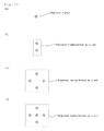
- FIGS. 10( a ) to 10 ( c ) are schematic illustrations for showing dispositions of alignment markers.
- FIG. 11 is a schematic illustration for showing alignment markers provided as a unit.
- FIGS. 12( a ) to 12 ( c ) are views schematically illustrating an embodiment wherein an alignment of photomask is performed by making use of visible light.
- FIG. 13( a ) is a cross sectional view schematically illustrating a flexible semiconductor device wherein the alignment marker extends to reach the lower principal surface of the insulating layer.
- FIG. 13( b ) is a plan view illustrating the flexible semiconductor device taken along a line Ic-Ic of FIG. 13( a ).
- FIG. 14 is a circuit diagram showing a drive circuit of an image display device according to an embodiment of the present invention.
- FIG. 15 is a plan view illustrating an exampled embodiment wherein the drive circuit of FIG. 14 is constructed by a flexible semiconductor device.
- FIG. 16 is a cross sectional view schematically illustrating an image display device according to an embodiment of the present invention.
- FIG. 17 is a cross sectional view schematically illustrating an image display device equipped with a color filter.
- FIGS. 18( a ) to 18 ( e ) are cross sectional views schematically illustrating the steps in a manufacturing process of an image display device according to the present invention.
- FIGS. 19( a ) to 19 ( d ) are cross sectional views schematically illustrating the steps in a manufacturing process of an image display device equipped with a color filter.
- FIG. 20 is a schematic view illustrating an example of a product (an image display part of a television) wherein the flexible semiconductor device is used.
- FIG. 21 is a schematic view illustrating an example of a product (an image display section of a cellular phone) wherein the flexible semiconductor device of the present invention is used.
- FIG. 22 is a schematic view illustrating an example of a product (an image display section of a mobile personal computer or a laptop computer) wherein the flexible semiconductor device of the present invention is used.
- FIG. 23 is a schematic view illustrating an example of a product (an image display section of a digital still camera) wherein the flexible semiconductor device of the present invention is used.
- FIG. 24 is a schematic view illustrating an example of a product (an image display section of a camcorder) wherein the flexible semiconductor device of the present invention is used.
- FIG. 25 is a schematic view illustrating an example of a product (an image display section of an electronic paper) wherein the flexible semiconductor device of the present invention is used.
- Each “direction” referred to in the present description means the direction based on the spacial relationship between the metal layer 10 and the semiconductor layer 30 , in which each of upward direction and downward direction is mentioned relating to the direction in the drawings for convenience. Specifically, the upward direction and the downward direction respectively correspond to the upward direction and the downward direction in each drawing.
- the side on which the semiconductor layer 30 is formed based on the metal layer 10 is referred to as “upward direction” and the side on which the semiconductor layer 30 is not formed based on the metal layer 10 is referred to as “downward direction”.
- FIG. 1( a ) is a schematic sectional structure of the flexible semiconductor device 100 whereas FIG. 1( b ) is a plan view of the device taken along a line Ib-Ib of FIG. 1( a ).
- the device of the present invention is a flexible semiconductor device 100 equipped with a flexible film.
- the flexible semiconductor device 100 comprises a semiconductor structure portion and a film layer 50 formed so as to cover the semiconductor structure portion. More specifically, the flexible semiconductor device 100 of the present invention comprises a metal layer 10 , an insulating layer 20 formed on the metal layer 10 , a semiconductor layer 30 formed on the insulating layer 20 , source and drain electrodes 40 s , 40 d formed on the insulating layer, source and drain electrodes being in contact with the semiconductor layer 30 , and a flexible film layer 50 formed such that the semiconductor layer 30 and the source and drain electrodes 40 s , 40 d are covered with the flexible film layer.
- the gate electrode 10 g is made of a part of the metal layer 10
- the gate insulating film 20 a is made of a part of the insulating layer 20 in the flexible semiconductor device 100 of the present invention.
- the film layer 50 of the flexible semiconductor device 100 has an opening 50 a and an opening 50 b formed therein.
- the opening 50 a extends between the upper surface of the semiconductor structure portion and the upper surface of the semiconductor device 100 .
- the opening 50 b extends between the upper surface of the insulating layer 20 and the upper surface of the semiconductor device 100 .
- the openings 50 a , 50 b are respectively provided with electrically-conductive parts formed therein.
- the electrically-conductive part in the opening 50 a serves as a contact via 60 a which connects between a circuit provided in a layer of the semiconductor structure portion and a circuit provided on the resin film.
- the electrically-conductive part in the opening 50 b serves not as the contact via but as an alignment marker 60 b (which will be described later) although it is similar to that of the opening 50 a in terms of the use of an electrically-conductive material.
- the flexible film layer 50 of the present invention 100 is provided with a plurality of vias extending in a thickness direction of the film layer, wherein at least one of the vias is the alignment marker (i.e., “positioning marker”).
- FIG. 1 illustrates an embodiment wherein only the via 60 b is the alignment marker
- FIG. 2 illustrates an embodiment wherein two vias ( 60 b , 60 b ′) are provided as the alignment markers.
- the film layer 50 is preferably made of a resin material which has flexibility. It is thus preferred that the flexible film layer 50 is a resin film.
- This resin film can serve as a supporting substrate for supporting the semiconductor structure portion (or TFT structure therewith) and is preferably made of a thermoplastic resin material or a thermosetting resin material having flexibility characteristic after being cured. Moreover, it is particularly preferred in the present invention that the resin film is adapted for the formation of the opening.
- the resin film preferably include at least one resin selected from the group consisting of an epoxy resin, a polyimide resin, an acrylic resin, a polyethylene terephthalate resin, a polyethylenenaphthalate resin, a polyphenylene sulfide resin, a polyphenylene ether resin, a liquid crystal polymer and a polytetrafluoroethylene.
- the resin film may be a polyimide film. These resin materials are excellent in the dimensional stability and thus is preferably used as a flexible material of the flexible semiconductor device.
- a laser processing may be adopted by using a carbon dioxide laser, YAG laser or the like.
- a photolithography may also be adopted so as to form the opening in the resin film.
- a resin material suitable for the photolithography e.g., resin film made of photosensitive resin
- an inorganic polymer material film e.g., a siloxane polymer film can be suitably used as the flexible film layer 50 since it has a flexibility and is appropriate for the formation of the opening.
- the flexible film layer may have a thickness of about 2 ⁇ m to about 100 ⁇ m and the adhesive material layer may have a thickness of about 3 ⁇ m to about 20 ⁇ m.
- the electrically-conductive part of the flexible semiconductor device 100 has an identification capability serving as the alignment marker as well as an electrically-conductive capability serving as a contact via.
- the electrically-conductive part comprises a metal component.
- the electrically-conductive parts i.e., vias 60 a , 60 b
- those made from an electroconductive paste material are preferable in terms of cost and productivity.
- the electroconductive paste material the paste material obtained by dispersing a single metal such as Au, Ag, Cu, Pt, Pd, Al and/or Pb, the mixture or alloy thereof, an electroconductive filler such as a carbon filler, a carbon nanotubes and the like into a binder which contains an organic resin (e.g., an epoxy resin) and/or a solvent (e.g., butylcarbitol acetate (BCA)).
- the electroconductive parts can be provided through filling the openings 50 a , 50 b with such electroconductive paste material.
- a metal e.g., Au, Ag, Cu, Ni, Co, Cr, Mn, Fe, Ru, Rh, Pd, Ag, Os, Ir and/or Pt
- a plating process for the purpose of forming the electrically-conductive parts (i.e., vias 60 a , 60 b ).
- a Cu plating process is preferred since it is comparatively inexpensive and the metal Cu in itself has a high electroconductivity.
- the metal Cu is preferred in terms of the identification capability upon the X-ray irradiation since it is a high-atomic-number-element.
- the semiconductor layer may be made of silicon (e.g., Si), germanium (Ge) and the like.
- the semiconductor layer may also be made of an oxide.
- the oxide of the oxide semiconductor may be an oxide of an elementary substance such as ZnO, SnO 2 , In 2 O 3 and/or TiO 2 , or a composite oxide such as InGaZnO, InSnO, InZnO and/or ZnMgO.
- a compound semiconductor may also be used, in which case a compound thereof is for example GaN, SiC, ZnSe, CdS and/or GaAs and so forth.
- an organic semiconductor may also be used, in which case an organic thereof is for example pentacene, poly-3-hexyl-thiophene, porphyrin derivatives, copper phthalocyanine and/or C60 and so forth.
- the flexible semiconductor device 100 of the present invention comprises the semiconductor structure portion which has been subjected to an annealing treatment. Specifically, it is preferred that, as a result of the heat treatment of the semiconductor layer 30 induced by the laser irradiation, a film quality of the semiconductor structure portion has been modified as compared with that before the laser irradiation.
- a component of the semiconductor layer may be modified from an amorphous silicon (before the irradiation) to a polycrystalline silicon (after the irradiation).
- Such polycrystalline silicon has its average particle diameter of a few hundred nm to about 2 micrometers, for example.
- the semiconductor layer 30 consists of polycrystalline silicon at the point in time before the laser irradiation
- the degree of the crystallization thereof can be improved by the irradiation.
- the modification of the film quality of the semiconductor structure portion can improve a mobility of the semiconductor layer 30 . This means that there may be a significant difference in the mobility of the semiconductor layer 30 between the before-irradiation and the after-irradiation.
- film quality substantially means the properties such as “crystalline condition”, “degree of crystallization” and/or “mobility” of the semiconductor layer.
- the modification of the film quality substantially means that “crystalline condition”, “degree of crystallization” and/or “mobility” change(s) or improve(s) as far as the semiconductor layer is concerned.
- the semiconductor properties can also be improved.
- the crystalline oxide semiconductor such as ZnO
- the performing of the annealing treatment makes it possible to improve the crystallinity of the oxide semiconductors (e.g., ZnO), which leads to an improved performance of the semiconductor.
- the formed layer when ZnO is formed by a RF magnetron sputtering process in the order of the formations of ZnO film (50 nm) and SiO 2 film (50 nm), the formed layer only shows as low mobility as 1 cm 2 /Vs or lower at the point in time before the excimer laser irradiation. While on the other hand, after the excimer laser irradiation, the layer becomes capable of functioning as the semiconductor and thus it can have a mobility of about 20 cm 2 /Vs.
- the effects of improving the semiconductor properties can be provided.
- an oxygen deficiency can be restored and thus the mobility can be improved due to the laser irradiation under the oxygen atmosphere (for example, air atmosphere).
- an oxide film e.g., SiO 2 or Al 2 O 2 film
- the oxygen deficiency of the amorphous oxide semiconductor can be restored due to an oxygen supplied thereto through the insulating layer 20 from the openings 50 a , 50 b .
- the very low mobility i.e., about 1 cm 2 /Vs or lower
- the very low mobility i.e., about 1 cm 2 /Vs or lower
- the very low mobility before the laser irradiation can be increased to the degree of about 10 cm 2 /Vs after the laser irradiation.
- the semiconductor structure portion is supported by the metal layer 10 .
- the metal layer 10 may consist of a metal foil. It is preferred that the metal which constitutes the metal foil 10 is a metal with an electric conductivity and a relatively high melting point. For example, copper (Cu, melting point: 1083° C.), nickel (Ni, melting point: 1453° C.), aluminum (Al, melting point: 660° C.) and/or stainless steel (SUS) may be used.
- Cu melting point: 1083° C.
- Ni nickel
- Al melting point: 660° C.
- SUS stainless steel
- the insulating film 20 made of an inorganic insulating material e.g., silicon oxide or silicon nitride
- the semiconductor layer 30 is formed on the insulating film 20 .
- the insulating layer 20 may be formed by oxidizing the surface of the metal layer 10 (e.g., metal foil). It is preferred in this case that a metal foil made of a valve metal (for example, an aluminum foil) is used as the metal layer 10 .
- An anodic oxide film can be formed on the surface of the metal foil by anodizing the valve metal thereof by using a chemical conversion solution, and thus this anodic oxide film may be used as the insulating layer 20 .
- This “anodic oxide film” is a very thin and densified oxide film, providing such an advantageous effect that the insulating layer 20 has no defect or the reduced degree of the defect.
- the material for the insulating layer 20 is not limited to the above, but any suitable materials may be used depending on the property required for the gate insulating film. For example, silicon oxide or silicon nitride may be used. As the material of the insulating layer 20 , not only the inorganic insulating material but also the other insulating materials such as organic insulating materials (e.g., polyimide) may be used.
- the gate electrode 10 g and wirings 10 a , 10 b are formed by the metal foil 10 serving as the support layer.
- the opening e.g., opening 10 ′
- the parts serving the gate electrode 10 g and wirings 10 a , 10 b are provided in the metal layer 10 .
- the source and drain electrodes 40 s , 40 d are in contact with the semiconductor layer 30 .
- a region located between the source electrode 40 s and the drain electrode 40 d functions as a channel region.
- Examples of the material to be used as the source and drain electrodes 40 s , 40 d include a metallic material such as gold (Au), silver (Ag), copper (Cu), nickel (Ni), chromium (Cr), cobalt (Co), magnesium (Mg), calcium (Ca), platinum (Pt), molybdenum (Mo), iron (Fe), zinc (Zn), titanium (Ti) and/or tungsten (W) and the like; an electrically-conductive oxide such as tin oxide (SnO 2 ), indium tin oxide (ITO), fluorine-containing tin oxide (PTO), ruthenium oxide (RuO 2 ), iridium oxide (IrO 2 ) and/or platinum oxide (PtO 2 ) and the like.
- Ag paste may be used to form the source and drain electrodes 40 s , 40 d .
- the source and drain electrodes 40 s , 40 d using such paste material may be formed by the printing technique (e.g., in
- a via opening 20 c in which an interlaminar connecting portion (via) 60 c may be provided.
- the interlaminar connecting portion (via) 60 c may be provided through a filling of an electrically material (e.g., Ag paste) into the via openings 20 c.
- the wiring 10 a is in connection with the drain electrode 40 d provided on the insulating layer 20 through the interlaminar connecting portion (via) 60 c .
- a part of the drain electrode 40 d may extend to the via opening 20 c , and thereby the interlaminar connecting portion (via) 60 c is provided.
- the gate electrode 10 g is provided below the channel region of the semiconductor layer 30 through the intervention of the gate insulating film 20 a . It is desired that the gate electrode and the channel region have the same size as each other, and they are positioned in an overlapping relation with each other with no misalignment. The reason for this will be described with reference to FIG. 3 . Supposing a case where the gate electrode 10 g and the channel 30 a are in misalignment with each other and another case where the gate electrode 10 g is smaller than the channel 30 a (see FIG. 3( a )), there is no portion of the gate electrode 10 g below the channel region 30 a in any of these cases.
- the parasitic capacitance can lead to such undesired problems that a waveform of the output signal can become not sharp, or the amount of the required current can be increased and thereby causing the power consumption to be increased.
- the same is true on the relationship between the gate electrode 10 g and drain electrode 40 d . Accordingly, it is desired that there is smaller overlapping between the gate electrode 40 g and the source electrode 40 s.
- the gate electrode 10 g and the channel region 30 a have the same size as each other and they are positioned in an overlapping relation with each other with no misalignment (see FIG. 3( c )).
- FIGS. 4( a ) to 4 ( e ), FIGS. 5( a ) to 5 ( d ), FIGS. 6( a ) to 6 ( c ) and FIGS. 7( a ) and 7 ( b ) respectively show cross-sectional views illustrating the steps in a manufacturing process of the flexible semiconductor device 100 .
- the step (i) is firstly performed. That is, an insulating layer is formed on one of principal surfaces of a metal foil.
- a metal foil 10 which serves as a support layer is firstly provided.
- a copper foil is provided.
- the metal foil 10 has a thickness preferably in the range of about 3 ⁇ m to about 100 ⁇ m, more preferably in the range of about 4 ⁇ m to about 20 ⁇ m, still more preferably in the range of about 8 ⁇ m to about 16 ⁇ m.
- an insulating layer 20 is formed on a surface of the metal foil 10 as shown in FIG. 4( b ).
- the insulating layer 20 may be provided by the “anodic oxidation of valve metal” as mentioned above (especially in a case where the metal foil is made of a valve metal).
- it is possible to form the insulating layer 20 by performing other methods.
- it can be formed by a sol gel process.
- the insulating layer 20 can be formed by applying (for example, spin-coating) an organic-inorganic hybrid material wherein organic molecules are bonded to the siloxane backbone, followed by calcinating it at about 300° C. to about 600° C.
- the thickness of the insulating layer 20 is approximately in the range of 0.1 ⁇ m to about 1 ⁇ m, for example.
- a via portion 60 c serving as an interlaminar connecting portion is formed in the insulating layer 20 .
- an opening 20 c may be formed at a formed region of the via 60 c , followed by filling an electrically-conductive material into the opening 20 c .
- a typical photolithography process may be performed for the formation of the opening 20 c .
- the etching of the insulating layer performed may be for example a dry etching using CF 3 .
- the step (ii) is performed. That is, a semiconductor layer is formed on the insulating layer, and then source and drain electrodes are formed such that the source and drain electrodes contact with the semiconductor layer. Specifically, the semiconductor layer 30 is firstly formed on the insulating layer 20 as shown in FIG. 4( c ).
- the thickness of the semiconductor layer may be approximately in the range of about 5 nm to about 990 nm (the thickness of the semiconductor structure portion may be for example approximately in the range of about 10 nm to about 1 ⁇ m).
- the formation of the semiconductor layer 30 can be performed for example by a thin film formation process such as a vacuum deposition process, a sputtering process and a plasma CVD process, as well as by a printing process such as a relief printing process, a gravure printing process, a screen printing process and an ink jet printing process.
- a thin film formation process such as a vacuum deposition process, a sputtering process and a plasma CVD process
- a printing process such as a relief printing process, a gravure printing process, a screen printing process and an ink jet printing process.
- a amorphous silicon-containing semiconductor layer 30 can be formed by applying a cyclic silane compound-containing solution (for example, cyclopentasilane-containing toluene solution) to the predetermined position on the insulating layer 20 with the ink jet printing process, followed by subjecting it to a heat treatment at about 300° C.
- the source and drain electrodes 40 s , 40 d are formed on the insulating layer 20 such that the source and drain electrodes 40 s , 40 d contact with the semiconductor layer 30 as shown in FIG. 4( d ).
- the drain electrode 40 d is disposed such that it extends to the position of the via portion 60 c .
- the drain electrode 40 d is formed such that one end of the drain electrode 40 d contacts with the via portion 60 c and the other end of the drain electrode 40 d contacts with the semiconductor layer 30 .
- Each of the source and drain electrodes has the thickness of about 50 nm to about 5 ⁇ m, for example.
- the formation of the source and drain electrodes 40 s , 40 d can be performed through an application of Ag paste by using of a printing process (e.g., a screen printing process, a gravure printing process, or an ink jet printing process).
- a printing process e.g., a screen printing process, a gravure printing process, or an ink jet printing process.
- the matter regarding the formation of the drain electrode can be similarly applied to that of the source electrode.
- the step (iii) is performed. That is, as shown in FIG. 4( e ), a flexible film layer 50 is formed so that the flexible film layer covers the semiconductor layer 30 and the source and drain electrodes 40 , 40 d .
- a resin film in a semi-cured condition is prepared wherein an adhesive material may be applied to the laminating surface of the resin film, and thereafter the prepared resin film is laminated onto the metal layer on which the semiconductor structure portion is provided.
- the laminate thus formed is then subject to a tentative bonding.
- the condition for the tentative bonding can be selected depending on the kinds of the semi-cured resin film and the adhesive material.
- the resin film composed of a polyimide film (thickness: about 12.5 ⁇ m) and an epoxy resin (thickness: about 10 ⁇ m) as the adhesive material applied to the laminating surface thereof
- the resin film and the metal foil are laminated onto each other and the resulting laminate is subject to a tentative pressure bonding under the heating condition of about 60° C. and the pressure condition of about 3 MPa.
- the thickness of the formed resin film 50 is for example in the range of about 4 ⁇ m to about 100 ⁇ m.
- the formation of the resin film 50 makes it possible to protect the semiconductor structure portion and also to safely perform a handling or conveying procedure in the subsequent steps such as the patterning treatment of the metal foil 10 and the like.
- the step (iv) is performed. That is, vias are formed in the flexible film layer, and thereby a semiconductor device precursor is provided. For example, as shown in FIGS. 5( a ) and 5 ( b ), openings 50 a , 50 b are formed in the flexible film layer 50 , and thereafter an electrically-conductive material is supplied into the resulting openings to form the vias 60 a , 60 b . The completion of the formation of the vias 60 a , 60 b produces the semiconductor device precursor 100 ′.
- the openings 50 a , 50 b of the resin film layer can be formed by a laser processing.
- a laser for the laser processing a carbon dioxide laser, a YAG laser, an excimer laser or the like may be used.
- the energy density may be in the range of about 50 mJ/cm 2 to about 500 mJ/cm 2 , for example.
- the opening 50 a used for the contact via can be formed by irradiating the resin film layer 50 with a laser so that a surface of a circuit electrode which is connected to the semiconductor structure portion is exposed.
- the opening 50 b used for the alignment marker can be formed by irradiating the resin film layer with the laser so that the upper surface of the insulating film in a form of metal film is exposed.
- each size (diameter) of the openings 50 a , 50 b can be controlled to a desired size by adjusting the diameter of the laser.
- the opening size (diameter) formed by the laser irradiation may be in the range of about 5 ⁇ m to about 80 ⁇ m.
- the diameter of the opening may be approximately 30 ⁇ m in its aperture plane.
- a desired beam diameter may be obtained not only by adjusting the diameter of the laser, but also by applying a mask to the laser beam.
- each of the openings 50 a , 50 b can be formed in a tapered shape (namely, there can be formed so-called “earthenware mortar form” or “inverted conical form” of the opening). That is, it is capable of forming an angle between the wall surface of each of the openings 50 a , 50 b and the top face of the resin film layer 50 to be an obtuse angle (i.e. larger than 90 degrees).
- the taper angle “ ⁇ ” as shown in FIG. 5( a ) can be in the range of about 110° to about 160°.
- each of the tapered openings 50 a , 50 b enables it to facilitate the filling process of the openings 50 a , 50 b with the use of the electroconductive material.
- the insulating layer made of the inorganic material (for example silica, i.e., SiO 2 ) can be additionally subjected to the laser processing.
- the formed opening can extend not only in the resin film 50 , but also in the insulating layer 20 . Namely, the formed opening can extend to reach the lower metal layer which corresponds to the lower face of the semiconductor structure portion.
- the alignment marker can be visible from below by means of visible light when the removal of the lower metal is performed. This is particularly preferable in a case where a functional layer is laminated onto the lower face of the flexible semiconductor device of the present invention.
- the method for forming the openings 50 a , 50 b is not limited to the laser processing.
- a punching process or mechanical drilling process may also be adopted for the formation of the openings.
- a photolithography process may also be adopted to form the openings in a case where the film is made of a light-sensitive polymer or the like.
- an electrically-conductive part is formed within each of the openings 50 a , 50 b .
- the electrically-conductive part is made from an electrically-conductive paste
- such electrically-conductive paste may be supplied into the openings 50 a , 50 b by a printing process for the purpose of forming the electrically-conductive part. More specifically, a print mask is disposed on a surface of the resin film 50 , and thereafter the openings 50 a , 50 b are filled with the electrically-conductive paste by means of a squeegee.
- the print mask is used for preventing a contamination of the surface of the resin film with the electrically-conductive paste, and thus the print mask is provided with holes formed therein, the holes corresponding to the openings of the resin film.
- a screen plate may be used.
- a PET film mask obtained by the PET film preliminarily laminated onto the surface of the resin film may also be used.
- the PET film is laminated onto the surface of the resin film, and thereafter the laser irradiation is performed with respect to the PET film.
- the PET film mask wherein the holes of the PET film and the openings of the resin film are in alignment with each other.
- the PET film mask in itself is finally removed after the filling of the electrically-conductive paste is completed.
- thermocompression bonding As shown in FIG. 5( c ), it is preferred that a metal foil 15 is disposed on the resin film 50 , and then a thermocompression bonding therebetween is performed (namely, a further metal layer 15 is preferably formed on the semiconductor device precursor 100 ′).
- the condition of the thermocompression bonding may be suitably selected depending on the kinds of the semi-cured resin film and the adhesive material.
- the metal foil 15 may be laminated onto the resin film 50 and thereafter the adhesive material may be subject to a substantial curing for about 1 hour under the condition of about 140° C. and about 5 MPa.
- the metal layer 15 can be formed by a plating process, which is preferable in terms of the productivity since the thermocompression bonding of the laminated metal foil can be eliminated.
- a Cu seed layer is firstly formed by performing an electroless copper plating, and subsequently the opening is filled with Cu material by performing an electrolytic copper plating.
- the electroless copper plating can be performed by immersing a sample into an electroless plating bath obtained by adding a formaldehyde as a reducing agent into a copper sulfate aqueous solution.
- the electrolytic plating can be performed by immersing the sample in a copper sulfate aqueous solution so that the sample is used as a cathode and the phosphorus-containing copper is used as an anode.
- a polyether compound, an organic sulfur compound and/or an amine compound can be added to the copper sulfate aqueous solution, and plating can be performed by applying an electric current of about 3 A/dm 2 (a resist layer may also be formed on the upper surface of the resin film such that holes of the resist layer is in alignment with the openings 50 b of the resin film).
- the step (v) is performed. That is, the metal foil 10 is subjected to a processing treatment, and thereby forming a gate electrode 10 g from the metal foil 10 . It is preferred that wirings 10 a , 10 b are also formed from the metal foil 10 upon the formation of the gate electrode 10 g from the metal foil 10 .
- a photo-resist film 11 is firstly formed on the metal foil at a position for the gate electrode and/or wiring to be formed. Specifically, as shown in FIG. 5( d ), the photo-resist film 11 is formed on the approximate whole of the lower surface of the metal foil 10 . Subsequently, as shown in FIG. 6( a ), a photomask 12 is disposed underneath the photo-resist film 11 . Subsequently, as shown in FIG. 6( b ), the photo-resist film 11 is subjected to a light-exposure treatment through the photomask 12 , and thereafter the developing treatment is performed to remove the unnecessary portions of the photo-resist film.
- the disposition of the photomask 12 is performed by superimposing the alignment marker 60 b of the resin film and a corresponding pattern of the photomask 12 onto each other (see FIGS. 6( a ) and 6 ( b )).
- the identification of the alignment marker of the resin film can be done for example by using a X-ray transmission image obtained by irradiating the semiconductor device precursor 100 ′ with a X-ray wherein the X-ray irradiation is performed above the semiconductor device precursor 100 ′ and thus the X-ray transmission image is obtained underneath the metal foil 10 .
- a lighter element i.e., an element with a lower atomic number
- a heavier element i.e., an element with a higher atomic number
- the metal conductive part i.e., position of alignment marker
- the metal foil 10 with the partially removed photo-resist film 11 ′ disposed thereon is subjected to an etching process, and thereby forming the gate electrode 10 g and wirings 10 a , 10 b from the metal foil 10 ( FIGS. 6( c ) and 7 ( a )).
- the method of the etching can be suitably selected depending on the kind of the metal foil. For example in a case where the metal foil is a copper foil, the etching can be performed by immersing it into an aqueous solution of iron chloride. Alternatively, the etching can be performed by a dry etching process (e.g., RIE).
- the partially removed photo-resist film 11 ′ used upon the developing treatment can be formed by the use of a direct light-exposure (see FIG. 8 ), instead of the use of the photomask.
- a direct light-exposure a desired position (pattern) of the photo-resist film is locally irradiated with the laser (e.g., laser with wavelength of 355 nm). That is, the photo-resist film is directly exposed to the light with no photomask disposed thereon.
- the position to be irradiated with the laser can be determined based on the identification of the alignment marker 60 b . Such identification of the alignment marker 60 b can be done similarly to that of the above use of the photomask.
- the direct light-exposure makes use of at least one of the vias of the semiconductor device precursor as an alignment marker in order to directly expose the desired position of the photo-resist film to the light without using the photomask.
- the alignment marker can be identified by using a visible light when a functional layer (e.g., image display layer) is aligned to be laminated onto both sides or one side of the semiconductor device.
- a functional layer e.g., image display layer
- Such alignment using the visible light is simple and is preferable since it can prevent a cumulative risk of the misalignment only by using the same alignment marker as that of the semiconductor device.
- the photo-resist on the metal foil 15 disposed on the upper surface of the resin film, and thereafter performing the etching process in order to form a desired wiring pattern 70 , image electrode 150 or the like (see FIG. 7( b )).
- the lower metal foil disposed underneath the lower surface of the semiconductor structure portion and the upper metal foil disposed on the resin film are individually performed. It is accordingly preferred that one of the metal foils is protected during the etching of the other metal foil by covering the whole surface of the other metal foil with the photo-resist.
- the kind and thickness of the upper and lower metal foils can be selected as appropriate.
- both of the upper and lower metal foils have the same material and the same thickness as each other (e.g., both of them are copper foils with their thickness of 12 ⁇ m) since the etching processes for the both of them can be performed at a time, making it possible to improve the productivity.
- Such concurrent etching process can be performed by immersing the upper and lower metal foils 10 , 15 with the patterned photo-resist films thereon into the etching solution in order to form the desired patterns of the metal foils 10 , 15 .
- the flexible semiconductor device 100 having the structure as shown in FIG. 7( b ) and FIG. 1 .
- the gate electrode 10 g is made of a part of the metal layer 10
- the gate insulating film 20 a is made of a part of the insulating layer 20 .
- a plurality of vias 60 a , 60 b , 60 c , . . . ) are provided such that they extend in a thickness direction of the layer 50 .
- the partially removed portion of the metal layer is provided at a position of at least one via (i.e., via 60 b in FIG. 7( b )).
- via 60 b a part of the metal foil, which part is in contact with the upper surface of the via 60 b , has been removed, and also another part of the metal foil, which another part is in contact with the lower surface of the via 60 b , has been also removed (the removed portions are indicated by the dashed lines).
- the via 60 b serving as the alignment marker extends from one of the principal surfaces of the flexible film layer 50 to the other of the principal surfaces of the flexible film layer 50 as shown in FIG. 7( b ).
- the openings 50 a , 50 b of the resin film layer 50 are filled with the electrically-conductive material (e.g., metal material) to form the electrically-conductive parts therefrom.
- the formation of the contact via and the formation of the alignment marker can be performed substantially by the same step at a time.
- the alignment marker in the present invention can be well identified by using the X-ray transmission image, making it possible to manufacture the TFT with no misalignment between the gate electrode and the channel.
- the present invention makes it possible to not only improve an efficiency of the manufacturing process but also improve the TFT performance by the alignment marker (i.e., the electrically-conductive part) provided in the resin film.
- the characterizing feature of the present invention i.e., “alignment” and “alignment marker” will be described in detail.
- the X-ray transmission image obtained by using the alignment marker is used upon the alignment of the photomask.
- the X-ray transmission image 110 obtained by irradiating the semiconductor device precursor 100 ′ with the X-ray is used, in which case via-corresponding points 120 in the X-ray transmission image are used as a positioning reference.
- the image points which correspond to the positions of the vias are used as the positioning reference, such image points being obtained by irradiating the semiconductor device precursor 100 ′ having the alignment markers 60 b , 60 b ′ with the X-ray.
- the alignment markers may be provided per light-exposure region.
- a set of the alignment markers e.g. two alignment markers or two units of the alignment markers
- the position of the alignment marker is not particularly limited. Take an embodiment where the alignment of the photomask is performed upon the disposing thereof as an example, the alignment markers may be disposed at the central region of the short side of the rectangular photomask. This makes it possible to minimalize the misalignment between the photomask and the work (i.e., a superimposition accuracy can be improved).
- the two alignment markers are measured by using the X-ray transmission image as described above, and thereby a centroid of the alignment region is determined, and also the assigned dimensions and error are corrected.
- the alignment of the photomask can be suitably performed by considering the values designed from the above centroid.
- the single via can serve as the alignment marker.
- the unit of a plurality of the vias can also serve as the alignment marker, as shown in FIGS. 11( a ) to 11 ( d ). That is, the four alignment markers may be disposed such that the unit (i.e., group) of them forms a square. Alternatively, the five alignment markers may be disposed such that the unit (i.e., group) of them forms a cross-like figure. As such, a plurality of the alignment markers may be disposed so that the unit (i.e., group) of them is in a desired form as a whole. This makes it possible to more clearly distinguish the alignment markers from the contact via, which leads to a desired image recognition.
- the alignment marker 60 b is formed such that it extends to the lower surface of the insulating layer 20 (see FIG. 12( a )), and thereafter the metal layer 10 and the photo-resist film are partially removed at a lower position of the alignment markers 60 b (see FIG. 12( b )).
- the position of the alignment marker 60 b can be identified when illuminating the lower side of the device precursor by means of the visible light (see FIG. 12( c )).
- the finally obtained flexible semiconductor device 100 b can have a structure as shown in FIG. 13 . Namely, as shown in FIG. 13 , the alignment marker 60 b of the flexible semiconductor device 100 b extends to the lower principal surface of the insulating layer 20 beyond the upper principal surface of the insulating layer 20 .
- FIG. 14 is a circuit diagram for explaining a drive circuit 90 of the image display device.
- FIG. 15 is a plan view of an example wherein the drive circuit is constructed by using the flexible semiconductor device 100 according to an embodiment of the present invention.
- the circuit 90 shown in FIG. 14 is a driving circuit which is mounted on an image display device (e.g., organic electroluminescence display), and FIG. 14 shows a constitution of one pixel in the image display device.
- Each pixel in the image display device according to the present invention comprises a circuit with a combination of two transistors ( 100 A, 100 B) and one capacitor 85 .
- This driving circuit includes a switching transistor 100 A (hereinafter, referred to as “Sw-Tr”) and a driving transistor 100 B (hereinafter, referred to as “Dr-Tr”), both of which consist of the flexible semiconductor device 100 of the present invention. It is possible that the structure of the flexible semiconductor device 100 is provided with a capacitor.
- a gate electrode of Sw-Tr 100 A is connected to a selection line 94 .
- the source electrode and the drain electrode of Sw-Tr 100 A one thereof is connected to a data line 92 and the other thereof is connected to a gate electrode of Dr-Tr 100 B.
- the source electrode and the drain electrode of Dr-Tr 100 B one thereof is connected to a power line 93 and the other thereof is connected to a display area 80 (e.g., an organic electroluminescence element).
- the capacitor 85 is connected to the region between the source electrode and the gate electrode of Dr-Tr 100 B.
- FIG. 15 is a plan view of the flexible semiconductor device in which a part of the circuit 90 shown in FIG. 14 is formed.
- FIG. 15( a ) is a plan view seen from the upper surface of the resin film.
- FIG. 15( b ) is a plan view wherein the metal layer and the resin film disposed on the resin film have been eliminated.
- FIG. 15( c ) is a plan view wherein the semiconductor structure portion and the electrically-conductive part as well as the insulating layer disposed on the metal foil have been further eliminated.
- the capacitor 85 which stores capacity is required in the drive circuit capable of driving an image display device.
- the capacitor is built in a part of the substrate structure, thus it is not necessary to arrange a capacitor separately to the exterior of the substrate structure. Therefore, it is possible to provide an image display device having a small size and high density mounting efficiency.
- the image display unit is produced by the transistor or a circuit comprising the transistors (particularly, an embodiment about the image display unit composed of a plurality of pixels over the flexible semiconductor device) will be explained.
- FIG. 16 is a sectional view of an OLED (organic electroluminescence) image display device 200 wherein three colors consisting of R (red), G (green) and B (blue) are used in three pixels on the flexible semiconductor device of the present invention.
- the semiconductor device is illustrated only by a resin film, pixel electrodes (cathodes) and the alignment markers.
- each light emitting layer 170 is arranged on each pixel electrode 150 consisting of R, G and B pixels where the luminescent materials of the light emitting layers respectively correspond to the respective ones of R, G and B.
- Pixel regulating parts 160 are provided between the adjacent pixels to prevent the adjacent luminescent materials from being intermingled with each other as well as to facilitate the positioning upon the supply of the EL materials.
- a transparent electrode layer (anode layer) 180 is provided over the light emitting layer 170 such that it covers the whole of each pixel.
- the materials to be used for the pixel electrodes 150 include a metal (e.g., Cu).
- the pixel electrode may have a stacked layer structure composed of a charge injection layer and a surface layer (e.g., Al surface layer with its thickness of 0.1 ⁇ m) wherein the charge injection layer functions to improve a charge injection efficiency with respect to the light emitting layer 170 , and the surface layer functions to improve a light extraction efficiency in upward direction by reflecting a light emitted from the light emitting layer.
- the pixel electrode may be a reflection electrode with Al/Cu stacked layer structure, for example.
- the material to be used for the light emitting layer 170 examples include, but not limited to, a polyfluorene-based electroluminescent material and a dendrimer-based light emitting material having a dendritically branched structure wherein at least one heavy metal (e.g., Ir or Pt) is positioned at the center of a dendron backbone of a so-called dendrimer.
- the light emitting layer 170 may have a single layer structure.
- the light emitting layer 170 may have a stacked layer structure with an electron injection layer/a light emitting layer/a hole injection layer wherein MoO 3 is used for the hole injection layer (to facilitate the injection of charge) and LiF is used for the electron injection layer.
- ITO may be used as the transparent electrode 180 of the anode.
- the pixel regulating part 160 it may be made of an insulating material.
- a photosensitive resin mainly comprising polyimide, or SiN can be used as the insulating material of the pixel regulating part 160 .
- the image display device may be configured to have a structure with a color filter as shown in FIG. 17 .
- the image display device 200 ′ as shown in FIG. 17 comprises the flexible semiconductor device 100 , a plurality of pixel electrodes 150 provided on the flexible semiconductor device 100 , a light emitting layer 170 provided such that it wholly covers the pixel electrodes 150 , a transparent electrode layer 180 provided on the light emitting layer 170 , and a color filter 190 provided on the transparent electrode layer 180 .
- the color filter 190 has a function to convert lights emitted from the light emitting layer 170 to three kinds of lights of red, green and blue, and thereby three kinds of pixels consisting of R (red), G (green) and B (blue) are provided.
- each of the light emitting layers separated by the pixel regulating parts 160 emits each of red, green and blue lights separately. While on the other hand, as for the image display device 200 ′ shown in FIG. 17 , the light emitted from the light emitting layer has no difference in color (i.e., the light emitting layer emits white light), but the passing of the light through the color filter 190 causes the generation of each of red, green and blue lights.
- the step (I) is performed. That is, the flexible semiconductor device 100 equipped with pixel electrodes 150 is prepared as shown in FIG. 18( a ).
- the pixel electrodes 150 can be provided by subjecting the metal foil 15 to a patterning treatment (that is, the pixel electrodes 150 can be formed by etching away the part of the metal foil provided on the flexible film layer by the photolithography process or the like) upon the manufacturing process of the flexible semiconductor device 100 .
- the pixel electrodes 150 can be provided by applying the raw materials for the pixel electrodes by a printing process or the like at predetermined portions upon the manufacturing process of the flexible semiconductor device 100 .
- step (II) is performed. That is, an image display unit composed of a plurality of pixels is formed over the flexible semiconductor device. For example, as shown in FIGS. 18( b ) to 18 ( d ), a plurality of pixel regulating parts 160 are formed on the flexible semiconductor device 100 , and then each light emitting layer 170 is formed on a region of each pixel electrode 150 , the region being partitioned by the pixel regulating parts 160 .
- the pixel regulating parts 160 can be formed, for example, by forming a precursor layer 160 ′ for the pixel regulating parts wherein the pixel electrodes as a whole are covered with a photosensitive resin material mainly consisting of polyimide, followed by subjecting the precursor layer 160 ′ to a photolithography process.
- Light emitting layers 170 of the predetermined colors are respectively formed on the corresponding ones of the pixel electrodes.
- the light emitting layers 170 can be formed, for example, by applying a solution of a polyfluorene-based electroluminescent material (1%) dissolved into xylene onto the pixel electrodes by performing an ink jet process.
- the light emitting layer 170 may have a thickness of about 80 nm, for example.
- the alignment markers 60 b , 60 b ′ of the flexible semiconductor device are preferably used. This is because the use of the alignment markers 60 b , 60 b ′ can effectively prevent a cumulative risk of the misalignment regarding the constituent elements of the image display device.
- Such partial removal of the metal foil enables the alignment marker to be identified by means of the visible light ray.
- the partial removal of the metal foil disposed on the alignment marker can be performed together with the patterning process of the metal foil, and thus the number of the processes is not substantially increased by such removal.
- a transparent electroconductive layer 180 (e.g., ITO film) is formed so as to cover the light emitting layers 170 .
- the transparent electroconductive layer consisting of the ITO film can be formed by performing a sputtering process.
- the manufacturing process of the image display device 200 ′ equipped with a color filter will now be explained.
- This manufacturing process is substantially the same as that of the above mentioned manufacturing process, while there are some partial differences. Specifically, after the step (I) as mentioned above (see, FIG. 19( a )), a light emitting layer 170 capable of emitting white color is wholly laminated in the form of a film (see FIG. 19( b )). Subsequently, a transparent electrode layer 180 is formed in the same manner as mentioned above (see FIG. 19( c )).
- the color filter 190 capable of emitting R (red), G (green) and B (blue) is formed such that each color of the filter is arranged at each of the corresponding pixel positions (see FIG. 19( d )).
- the image display device 200 ′ Upon the arrangement of the color filter 190 , the alignment markers 60 b , 60 b ′ of the flexible semiconductor device can be used.
- the use of the alignment markers 60 b , 60 b ′ can effectively prevent a cumulative risk of the misalignment regarding the constituent elements of the image display device. In this regard, the removal of a part of the metal foil is preferred, the part being provided on the alignment marker.
- the manufacturing method of the flexible semiconductor device of the present invention is excellent in the productivity of a flexible semiconductor device.
- the resulting flexible semiconductor device can also be used for various image display parts (i.e., image display device), and also can be used for an electronic paper, a digital paper and so forth.
- the flexible semiconductor device can be used for a television picture indicator as shown in FIG. 20 , the image display part of a cellular phone as shown in FIG. 21 , the image display part of a mobile personal computer or a notebook computer as shown in FIG. 22 , the image display part of a digital still camera and a camcorder as shown in FIGS. 23 and 24 , the image display part of an electronic paper as shown in FIG. 25 and so forth.
- the flexible semiconductor device obtained by the manufacturing method of the present invention can also be adapted for the various uses (for example, RF-ID, a memory, MPU, a solar battery, a sensor and so forth) which application is now considered to be adapted by the printing electronics.
Landscapes
- Engineering & Computer Science (AREA)
- Microelectronics & Electronic Packaging (AREA)
- Power Engineering (AREA)
- Physics & Mathematics (AREA)
- General Physics & Mathematics (AREA)
- Condensed Matter Physics & Semiconductors (AREA)
- Computer Hardware Design (AREA)
- Ceramic Engineering (AREA)
- Manufacturing & Machinery (AREA)
- Chemical & Material Sciences (AREA)
- Crystallography & Structural Chemistry (AREA)
- Theoretical Computer Science (AREA)
- Thin Film Transistor (AREA)
- Electroluminescent Light Sources (AREA)
- Devices For Indicating Variable Information By Combining Individual Elements (AREA)
- Internal Circuitry In Semiconductor Integrated Circuit Devices (AREA)
Abstract
Description
- [Patent document 1] Japanese Unexamined Patent Publication (Kokai) No. 2007-67263; and
- [Patent document 2] Japanese Unexamined Patent Publication (Kokai) No. 2004-297084.
-
- (v1) forming a photo-resist film on the other of the principal surfaces of the metal foil;
- (v2) subjecting the photo-resist film to a light-exposure treatment and a developing treatment, and thereby removing at least part of the photo-resist film; and
- (v3) subjecting the metal foil to an etching treatment via the photo-resist film at least part of which has been removed, and thereby forming the gate electrode from the metal foil,
- 10: Metal layer or metal foil (Lower metal layer or lower metal foil)
- 10 g: Gate electrode
- 10 a, 10 b: Wiring made of metal layer
- 12: Photomask
- 15: Metal layer or metal foil (Upper metal layer or upper metal foil)
- 20: Insulating layer (Insulating film)
- 20 a: Gate insulating film (Gate insulating layer)
- 20 c: Via opening provided in insulating layer
- 30: Semiconductor layer
- 40 s, 40 d: Source electrode, Drain electrode
- 50: Flexible film layer
- 50 a, 50 b: Openings provided in flexible film layer
- 60: Via
- 60 a: Contact via (Via)
- 60 b: Alignment marker (Via)
- 60 c: Interlaminar connecting portion
- 70: Wiring layer and/or Pixel electrode
- 80: Display portion
- 82: Wiring
- 85: Capacitor
- 90: Driving circuit
- 92: Data line
- 93: Power-supply line
- 94: Selection line
- 100, 100 a, 100 b: Flexible semiconductor device
- 100′: Semiconductor device precursor
- 110: X-ray transmission image
- 120: Via-corresponding point
- 150: Pixel electrode
- 160: Pixel regulating part
- 160′: Pixel regulating part precursor
- 165: Photomask used for formation of pixel regulating part
- 170: Light emitting layer
- 180: Transparent electrode layer
- 190: Color filter
- 200: Image display device
- 200′: Image display device
-
- When the photomask is disposed per one transistor, the alignment markers are disposed per such one transistor (
FIG. 10( a)). - When the photomask is disposed per one group of a plurality of transistors, the alignment markers are disposed per such one group (
FIG. 10( b)). - When all the transistors in the work are subjected to the light-exposure and developing treatments by using one photomask, a set of the alignment markers are disposed per such work (
FIG. 10( c)).
- When the photomask is disposed per one transistor, the alignment markers are disposed per such one transistor (
-
- Instead of the embodiment where the contact via and the alignment marker are individually provided, another embodiment may be possible where a part of the contact vias is the alignment marker(s).
- Instead of the embodiment where the alignment marker has a form of “via”, another embodiment may be possible where the alignment marker has a form of “through-hole” in which metal film (e.g., copper film) may be provided on an inner-wall surface of the opening by a non-electrolytic plating.
- The present invention is not particularly limited to the embodiment where the resin film is laminated to form the flexible film layer of the flexible semiconductor device. Another embodiment may be possible where the formation of the flexible film layer is performed through an application (e.g., spin coating) of a semi-cured resin material or a photosensitive resin material.
- Each pixel may comprise not only two TFT elements (the first TFT element and the second TFT element) but also more than two elements depending on the constructional design of the display. As a result, the flexible semiconductor device of the present embodiment may be modified according to such constructional design.
- In each of the above embodiments, although the present invention has been described with respect to the flexible semiconductor device which is mounted on an organic EL display, the flexible semiconductor device of the present invention may be mounted on an inorganic EL display. Moreover, the flexible semiconductor device may be mounted not only on the EL display but also on an electronic paper. Furthermore, it is possible that the flexible semiconductor device of the present invention is mounted not only on the display device but also on communication facilities (e.g., RFID), memories and so on.
- The several embodiments wherein each one flexible semiconductor device is manufactured in the form corresponding to one device have been described above. While not being limited thereto, the present invention can be performed such that the flexible semiconductor devices are manufactured in the form corresponding to two or more devices. As an example of such manufacturing form, a roll-to-roll process may be adopted.
Claims (31)
Applications Claiming Priority (3)
| Application Number | Priority Date | Filing Date | Title |
|---|---|---|---|
| JP2011-066139 | 2011-03-24 | ||
| JP2011066139 | 2011-03-24 | ||
| PCT/JP2012/001151 WO2012127779A1 (en) | 2011-03-24 | 2012-02-21 | Flexible semiconductor device and method for producing same |
Publications (2)
| Publication Number | Publication Date |
|---|---|
| US20130168681A1 US20130168681A1 (en) | 2013-07-04 |
| US8993387B2 true US8993387B2 (en) | 2015-03-31 |
Family
ID=46878962
Family Applications (1)
| Application Number | Title | Priority Date | Filing Date |
|---|---|---|---|
| US13/821,352 Active 2032-07-31 US8993387B2 (en) | 2011-03-24 | 2012-02-21 | Flexible semiconductor device, method for manufacturing the same, image display device using the same and method for manufacturing the image display device |
Country Status (5)
| Country | Link |
|---|---|
| US (1) | US8993387B2 (en) |
| JP (1) | JP5842180B2 (en) |
| KR (1) | KR20140024789A (en) |
| CN (1) | CN102812540B (en) |
| WO (1) | WO2012127779A1 (en) |
Families Citing this family (6)
| Publication number | Priority date | Publication date | Assignee | Title |
|---|---|---|---|---|
| CN104659038A (en) * | 2015-03-13 | 2015-05-27 | 京东方科技集团股份有限公司 | Display backboard, method for manufacturing the display backboard, and display device |
| JP6050414B2 (en) * | 2015-03-30 | 2016-12-21 | 日本写真印刷株式会社 | Thin film transistor manufacturing method and thin film transistor |
| US10003023B2 (en) * | 2016-04-15 | 2018-06-19 | Semiconductor Energy Laboratory Co., Ltd. | Display device and electronic device |
| US10867890B2 (en) * | 2018-09-27 | 2020-12-15 | Taiwan Semiconductor Manufacturing Company, Ltd. | Mutli-chip package with encapsulated conductor via |
| CN109643700B (en) | 2018-11-21 | 2019-09-10 | 长江存储科技有限责任公司 | Method, device and structure for the engagement alignment mark at joint interface |
| CN111681990B (en) * | 2020-07-27 | 2023-04-07 | 合肥鑫晟光电科技有限公司 | Preparation method of display substrate, display substrate and display device |
Citations (9)
| Publication number | Priority date | Publication date | Assignee | Title |
|---|---|---|---|---|
| JPH07302881A (en) | 1994-04-28 | 1995-11-14 | Mitsubishi Electric Corp | Semiconductor device, and method of forming fault analysis mark |
| US5821138A (en) | 1995-02-16 | 1998-10-13 | Semiconductor Energy Laboratory Co., Ltd. | Method of manufacturing a semiconductor device using a metal which promotes crystallization of silicon and substrate bonding |
| JP2000305109A (en) | 1999-04-16 | 2000-11-02 | Seiko Epson Corp | Manufacture of electrooptical device and electrooptical device |
| JP2005236186A (en) | 2004-02-23 | 2005-09-02 | Seiko Epson Corp | Semiconductor device, manufacturing method thereof, and electronic equipment |
| JP2007067263A (en) | 2005-09-01 | 2007-03-15 | Konica Minolta Holdings Inc | Organic semiconductor material, organic semiconductor film, organic semiconductor device and organic semiconductor thin-film transistor |
| JP2010145772A (en) | 2008-12-19 | 2010-07-01 | Sony Corp | Display device and electronic apparatus |
| JP2010238873A (en) | 2009-03-31 | 2010-10-21 | Panasonic Corp | Flexible semiconductor device and method for manufacturing the same |
| US20130292666A1 (en) * | 2011-01-20 | 2013-11-07 | Sharp Kabushiki Kaisha | Substrate on which film is formed, and organic el display device |
| US8847229B2 (en) * | 2011-03-24 | 2014-09-30 | Panasonic Corporation | Flexible semiconductor device, method for manufacturing the same, image display device using the same and method for manufacturing the image display device |
Family Cites Families (1)
| Publication number | Priority date | Publication date | Assignee | Title |
|---|---|---|---|---|
| KR100715943B1 (en) * | 2001-01-29 | 2007-05-08 | 삼성전자주식회사 | Liquid crystal display device and method for manufacturing the same |
-
2012
- 2012-02-21 JP JP2012538898A patent/JP5842180B2/en active Active
- 2012-02-21 US US13/821,352 patent/US8993387B2/en active Active
- 2012-02-21 WO PCT/JP2012/001151 patent/WO2012127779A1/en active Application Filing
- 2012-02-21 CN CN201280000786.6A patent/CN102812540B/en active Active
- 2012-02-21 KR KR1020127022898A patent/KR20140024789A/en not_active Application Discontinuation
Patent Citations (16)
| Publication number | Priority date | Publication date | Assignee | Title |
|---|---|---|---|---|
| JPH07302881A (en) | 1994-04-28 | 1995-11-14 | Mitsubishi Electric Corp | Semiconductor device, and method of forming fault analysis mark |
| US7361519B2 (en) | 1995-02-16 | 2008-04-22 | Semiconductor Energy Laboratory Co., Ltd. | Method of manufacturing a semiconductor device |
| US5821138A (en) | 1995-02-16 | 1998-10-13 | Semiconductor Energy Laboratory Co., Ltd. | Method of manufacturing a semiconductor device using a metal which promotes crystallization of silicon and substrate bonding |
| US6376333B1 (en) | 1995-02-16 | 2002-04-23 | Semiconductor Energy Laboratory Co., Ltd. | Method of manufacturing flexible display with transfer from auxiliary substrate |
| JP2004297084A (en) | 1995-02-16 | 2004-10-21 | Semiconductor Energy Lab Co Ltd | Method for manufacturing semiconductor device |
| US20080309585A1 (en) | 1995-02-16 | 2008-12-18 | Semiconductor Energy Laboratory Co., Ltd. | Method of manufacturing a semiconductor device |
| US6998282B1 (en) | 1995-02-16 | 2006-02-14 | Semiconductor Energy Laboratory Co., Ltd. | Method of manufacturing a semiconductor device |
| US7375782B2 (en) | 1995-02-16 | 2008-05-20 | Semiconductor Energy Laboratory Co., Ltd. | Method of manufacturing a semiconductor device |
| JP2000305109A (en) | 1999-04-16 | 2000-11-02 | Seiko Epson Corp | Manufacture of electrooptical device and electrooptical device |
| US7288792B2 (en) | 2004-02-23 | 2007-10-30 | Seiko Epson Corporation | Method of manufacturing semiconductor device, method of manufacturing electronic apparatus, semiconductor device, and electronic apparatus |
| JP2005236186A (en) | 2004-02-23 | 2005-09-02 | Seiko Epson Corp | Semiconductor device, manufacturing method thereof, and electronic equipment |
| JP2007067263A (en) | 2005-09-01 | 2007-03-15 | Konica Minolta Holdings Inc | Organic semiconductor material, organic semiconductor film, organic semiconductor device and organic semiconductor thin-film transistor |
| JP2010145772A (en) | 2008-12-19 | 2010-07-01 | Sony Corp | Display device and electronic apparatus |
| JP2010238873A (en) | 2009-03-31 | 2010-10-21 | Panasonic Corp | Flexible semiconductor device and method for manufacturing the same |
| US20130292666A1 (en) * | 2011-01-20 | 2013-11-07 | Sharp Kabushiki Kaisha | Substrate on which film is formed, and organic el display device |
| US8847229B2 (en) * | 2011-03-24 | 2014-09-30 | Panasonic Corporation | Flexible semiconductor device, method for manufacturing the same, image display device using the same and method for manufacturing the image display device |
Non-Patent Citations (2)
| Title |
|---|
| International Preliminary Report on Patentability and Written Opinion of the International Searching Authority issued Oct. 3, 2013 in International (PCT) Application No. PCT/JP2012/001151. |
| International Search Report issued Apr. 17, 2012 in International (PCT) Application No. PCT/JP2012/001151. |
Also Published As
| Publication number | Publication date |
|---|---|
| JPWO2012127779A1 (en) | 2014-07-24 |
| CN102812540A (en) | 2012-12-05 |
| KR20140024789A (en) | 2014-03-03 |
| US20130168681A1 (en) | 2013-07-04 |
| CN102812540B (en) | 2016-01-20 |
| JP5842180B2 (en) | 2016-01-13 |
| WO2012127779A1 (en) | 2012-09-27 |
Similar Documents
| Publication | Publication Date | Title |
|---|---|---|
| US8847229B2 (en) | Flexible semiconductor device, method for manufacturing the same, image display device using the same and method for manufacturing the image display device | |
| US8975626B2 (en) | Flexible semiconductor device | |
| US8895373B2 (en) | Method for manufacturing flexible semiconductor device having gate electrode disposed within an opening of a resin film | |
| US20120286264A1 (en) | Flexible semiconductor device, method for manufacturing the same and image display device | |
| US8993387B2 (en) | Flexible semiconductor device, method for manufacturing the same, image display device using the same and method for manufacturing the image display device | |
| US20120280229A1 (en) | Flexible semiconductor device, method for manufacturing the same and image display device | |
| US8525172B2 (en) | Flexible semiconductor device | |
| CN102593380B (en) | Semiconductor device and manufacture method thereof | |
| CN101442106B (en) | Semiconductor device, method for manufacturing the same, liquid crystal television, and EL television | |
| JP2009025453A (en) | Display panel and its manufacture method | |
| JP4785396B2 (en) | Method for manufacturing semiconductor device | |
| JP2009054539A (en) | Display device and its manufacturing method | |
| CN113421903A (en) | Display substrate, preparation method thereof, display panel and display device | |
| CN114420711A (en) | Display substrate, preparation method thereof and display device |
Legal Events
| Date | Code | Title | Description |
|---|---|---|---|
| AS | Assignment |
Owner name: PANASONIC CORPORATION, JAPAN Free format text: ASSIGNMENT OF ASSIGNORS INTEREST;ASSIGNORS:SUZUKI, TAKESHI;HIRANO, KOICHI;MASUDA, SHINOBU;REEL/FRAME:030470/0546 Effective date: 20130118 |
|
| AS | Assignment |
Owner name: PANASONIC INTELLECTUAL PROPERTY MANAGEMENT CO., LTD., JAPAN Free format text: ASSIGNMENT OF ASSIGNORS INTEREST;ASSIGNOR:PANASONIC CORPORATION;REEL/FRAME:034194/0143 Effective date: 20141110 Owner name: PANASONIC INTELLECTUAL PROPERTY MANAGEMENT CO., LT Free format text: ASSIGNMENT OF ASSIGNORS INTEREST;ASSIGNOR:PANASONIC CORPORATION;REEL/FRAME:034194/0143 Effective date: 20141110 |
|
| STCF | Information on status: patent grant |
Free format text: PATENTED CASE |
|
| FEPP | Fee payment procedure |
Free format text: PAYOR NUMBER ASSIGNED (ORIGINAL EVENT CODE: ASPN); ENTITY STATUS OF PATENT OWNER: LARGE ENTITY |
|
| MAFP | Maintenance fee payment |
Free format text: PAYMENT OF MAINTENANCE FEE, 4TH YEAR, LARGE ENTITY (ORIGINAL EVENT CODE: M1551); ENTITY STATUS OF PATENT OWNER: LARGE ENTITY Year of fee payment: 4 |
|
| AS | Assignment |
Owner name: PANASONIC INTELLECTUAL PROPERTY MANAGEMENT CO., LTD., JAPAN Free format text: CORRECTIVE ASSIGNMENT TO CORRECT THE ERRONEOUSLY FILED APPLICATION NUMBERS 13/384239, 13/498734, 14/116681 AND 14/301144 PREVIOUSLY RECORDED ON REEL 034194 FRAME 0143. ASSIGNOR(S) HEREBY CONFIRMS THE ASSIGNMENT;ASSIGNOR:PANASONIC CORPORATION;REEL/FRAME:056788/0362 Effective date: 20141110 |
|
| MAFP | Maintenance fee payment |
Free format text: PAYMENT OF MAINTENANCE FEE, 8TH YEAR, LARGE ENTITY (ORIGINAL EVENT CODE: M1552); ENTITY STATUS OF PATENT OWNER: LARGE ENTITY Year of fee payment: 8 |