US9024482B2 - Power feeding device and wireless power feeding system - Google Patents

Power feeding device and wireless power feeding system Download PDF

Info

Publication number
US9024482B2
US9024482B2 US13/352,383 US201213352383A US9024482B2 US 9024482 B2 US9024482 B2 US 9024482B2 US 201213352383 A US201213352383 A US 201213352383A US 9024482 B2 US9024482 B2 US 9024482B2
Authority
US
United States
Prior art keywords
power
circuit
power feeding
coil
wireless
Prior art date
Legal status (The legal status is an assumption and is not a legal conclusion. Google has not performed a legal analysis and makes no representation as to the accuracy of the status listed.)
Active, expires
Application number
US13/352,383
Other versions
US20120187771A1 (en
Inventor
Koichiro Kamata
Shinya Okano
Misako Sato
Shuhei Maeda
Current Assignee (The listed assignees may be inaccurate. Google has not performed a legal analysis and makes no representation or warranty as to the accuracy of the list.)
Semiconductor Energy Laboratory Co Ltd
Original Assignee
Semiconductor Energy Laboratory Co Ltd
Priority date (The priority date is an assumption and is not a legal conclusion. Google has not performed a legal analysis and makes no representation as to the accuracy of the date listed.)
Filing date
Publication date
Application filed by Semiconductor Energy Laboratory Co Ltd filed Critical Semiconductor Energy Laboratory Co Ltd
Assigned to SEMICONDUCTOR ENERGY LABORATORY CO., LTD. reassignment SEMICONDUCTOR ENERGY LABORATORY CO., LTD. ASSIGNMENT OF ASSIGNORS INTEREST (SEE DOCUMENT FOR DETAILS). Assignors: MAEDA, SHUHEI, OKANO, SHINYA, SATO, MISAKO, KAMATA, KOICHIRO
Publication of US20120187771A1 publication Critical patent/US20120187771A1/en
Priority to US14/680,169 priority Critical patent/US9837977B2/en
Application granted granted Critical
Publication of US9024482B2 publication Critical patent/US9024482B2/en
Priority to US15/825,405 priority patent/US10491183B2/en
Active legal-status Critical Current
Adjusted expiration legal-status Critical

Links

Images

Classifications

    • H02J7/025
    • HELECTRICITY
    • H02GENERATION; CONVERSION OR DISTRIBUTION OF ELECTRIC POWER
    • H02JCIRCUIT ARRANGEMENTS OR SYSTEMS FOR SUPPLYING OR DISTRIBUTING ELECTRIC POWER; SYSTEMS FOR STORING ELECTRIC ENERGY
    • H02J50/00Circuit arrangements or systems for wireless supply or distribution of electric power
    • H02J50/10Circuit arrangements or systems for wireless supply or distribution of electric power using inductive coupling
    • H02J50/12Circuit arrangements or systems for wireless supply or distribution of electric power using inductive coupling of the resonant type
    • HELECTRICITY
    • H01ELECTRIC ELEMENTS
    • H01FMAGNETS; INDUCTANCES; TRANSFORMERS; SELECTION OF MATERIALS FOR THEIR MAGNETIC PROPERTIES
    • H01F38/00Adaptations of transformers or inductances for specific applications or functions
    • H01F38/14Inductive couplings
    • HELECTRICITY
    • H02GENERATION; CONVERSION OR DISTRIBUTION OF ELECTRIC POWER
    • H02JCIRCUIT ARRANGEMENTS OR SYSTEMS FOR SUPPLYING OR DISTRIBUTING ELECTRIC POWER; SYSTEMS FOR STORING ELECTRIC ENERGY
    • H02J50/00Circuit arrangements or systems for wireless supply or distribution of electric power
    • H02J50/005Mechanical details of housing or structure aiming to accommodate the power transfer means, e.g. mechanical integration of coils, antennas or transducers into emitting or receiving devices
    • HELECTRICITY
    • H02GENERATION; CONVERSION OR DISTRIBUTION OF ELECTRIC POWER
    • H02JCIRCUIT ARRANGEMENTS OR SYSTEMS FOR SUPPLYING OR DISTRIBUTING ELECTRIC POWER; SYSTEMS FOR STORING ELECTRIC ENERGY
    • H02J50/00Circuit arrangements or systems for wireless supply or distribution of electric power
    • H02J50/40Circuit arrangements or systems for wireless supply or distribution of electric power using two or more transmitting or receiving devices
    • HELECTRICITY
    • H02GENERATION; CONVERSION OR DISTRIBUTION OF ELECTRIC POWER
    • H02JCIRCUIT ARRANGEMENTS OR SYSTEMS FOR SUPPLYING OR DISTRIBUTING ELECTRIC POWER; SYSTEMS FOR STORING ELECTRIC ENERGY
    • H02J50/00Circuit arrangements or systems for wireless supply or distribution of electric power
    • H02J50/80Circuit arrangements or systems for wireless supply or distribution of electric power involving the exchange of data, concerning supply or distribution of electric power, between transmitting devices and receiving devices
    • HELECTRICITY
    • H03ELECTRONIC CIRCUITRY
    • H03CMODULATION
    • H03C1/00Amplitude modulation
    • H03C1/36Amplitude modulation by means of semiconductor device having at least three electrodes
    • HELECTRICITY
    • H03ELECTRONIC CIRCUITRY
    • H03DDEMODULATION OR TRANSFERENCE OF MODULATION FROM ONE CARRIER TO ANOTHER
    • H03D1/00Demodulation of amplitude-modulated oscillations
    • H03D1/02Details
    • HELECTRICITY
    • H03ELECTRONIC CIRCUITRY
    • H03HIMPEDANCE NETWORKS, e.g. RESONANT CIRCUITS; RESONATORS
    • H03H7/00Multiple-port networks comprising only passive electrical elements as network components
    • H03H7/38Impedance-matching networks
    • H04B5/79
    • HELECTRICITY
    • H01ELECTRIC ELEMENTS
    • H01FMAGNETS; INDUCTANCES; TRANSFORMERS; SELECTION OF MATERIALS FOR THEIR MAGNETIC PROPERTIES
    • H01F38/00Adaptations of transformers or inductances for specific applications or functions
    • H01F38/14Inductive couplings
    • H01F2038/146Inductive couplings in combination with capacitive coupling
    • HELECTRICITY
    • H02GENERATION; CONVERSION OR DISTRIBUTION OF ELECTRIC POWER
    • H02JCIRCUIT ARRANGEMENTS OR SYSTEMS FOR SUPPLYING OR DISTRIBUTING ELECTRIC POWER; SYSTEMS FOR STORING ELECTRIC ENERGY
    • H02J50/00Circuit arrangements or systems for wireless supply or distribution of electric power
    • H02J50/90Circuit arrangements or systems for wireless supply or distribution of electric power involving detection or optimisation of position, e.g. alignment

Definitions

  • the present invention relates to power feeding devices and wireless power feeding systems including the power feeding devices.
  • Mobile phones, digital video cameras, and electric propulsion vehicles include batteries which are energy storage means. At the moment, the batteries are charged in most cases by being directly connected to home AC sources which are power feeding means. Other devices that have no battery or do not use power charged in a battery are directly supplied with power from a home AC source through a wiring or the like.
  • Typical methods are ah electromagnetic induction method (also referred to as an electromagnetic coupling method), a radio wave method (also referred to as a microwave method), and a resonance method.
  • An electromagnetic induction method comes into wide use for some electronic device, such as small consumer electronics.
  • a resonant wireless power feeding system has attracted attention since it provides high transmission efficiency at middle and long distance.
  • power transmission efficiency changes enormously depending on the distance between a resonant coil included in a device that receives power (hereinafter “power reception device”) and a resonant coil included in a device that supplies power (hereinafter “power feeding device”).
  • power reception device a resonant coil included in a device that receives power
  • power feeding device a resonant coil included in a device that supplies power
  • Patent Document 1 Japanese Published Patent Application No. 2010-252468
  • Patent Document 2 Japanese Published Patent Application No. 2010-239690
  • FIGS. 8 A 1 , 8 B 1 , and 8 C 1 are schematic diagrams illustrating a first coil 901 and a first resonant coil 902 in a power feeding device and a second coil 903 and a second resonant coil 904 in a power reception device; these coils are positioned between a high frequency power source 900 and a load 910 .
  • FIGS. 8 A 1 , 8 B 1 , and 8 C 1 schematically show the distance between the first resonant coil 902 in the power feeding device and the second resonant coil 904 in the power reception device.
  • FIG. 8 A 1 , 8 B 1 , and 8 C 1 schematically show the distance between the first resonant coil 902 in the power feeding device and the second resonant coil 904 in the power reception device.
  • FIG. 8 A 1 shows a state where these resonant coils are placed at a distance less than the optimal distance for resonance.
  • FIG. 8 B 1 shows a state where the resonant coils are placed at the optimal distance for resonance.
  • FIG. 8 C 1 shows a state where the resonant coils are placed at a distance greater than the optimal distance for resonance.
  • FIGS. 8 A 2 , 8 B 2 , and 8 C 2 are graphs showing dependence of transmission efficiency between the power feeding device and the power reception device on oscillation frequency of the high frequency power source 900 , which correspond to FIGS. 8 A 1 , 8 B 1 , and 8 C 1 .
  • the frequency f 0 in the graphs is the resonant frequency of the resonant coils.
  • the power transmission efficiency is at the maximum with the frequency f 0 as shown in FIG. 8 B 2 .
  • the peak of the power transmission efficiency is split and the efficiency reaches its peak with the frequency f 0 ′ as shown in FIG. 8 A 2 .
  • the frequency f 0 in FIG. 8 A 2 is in the valley between the two peaks, which means that the power transmission efficiency is decreased with the frequency f 0 .
  • an object of one embodiment of the present invention is to provide a resonant power feeding system that can provide high power transmission efficiency between a power feeding device and a power reception device without dynamically controlling the oscillation frequency in accordance with the distance between the power feeding device and the power reception device.
  • high power transmission efficiency between a power feeding device and a power reception device is obtained by addition of a structure for adjusting the matching condition in both the power reception device and the power feeding device.
  • a transmission-reception circuit and a matching circuit are provided in both the power reception device and the power feeding device, and wireless signals for adjusting the matching circuit are transmitted and received through a resonant coil.
  • the power feeding device can efficiently supply power to the power reception device without adjusting the oscillation frequency.
  • a power feeding device includes a first resonant coil resonating with a second resonant coil electromagnetically coupled to a second coil in a power reception device; a first coil electromagnetically coupled to the first resonant coil; a transmission-reception circuit including a modulation circuit configured to modulate an alternating-current signal output from a high frequency power source in order to superimpose a data signal on the alternating-current signal to produce a first wireless signal, and a demodulation circuit configured to demodulate a second wireless signal received by the first coil from the power reception device; a matching circuit configured to match impedance between the high frequency power source side and the first coil side; and a control circuit configured to control the matching circuit in accordance with a power value detected by the power reception device and included in the second wireless signal received by the first coil, and to generate a data signal of the first wireless signal superimposed on the alternating-current signal.
  • a wireless power feeding system includes a power feeding device and a power reception device.
  • the power feeding device includes a first resonant coil; a first coil electromagnetically coupled to the first resonant coil; a first transmission-reception circuit including a modulation circuit configured to modulate an alternating-current signal output from a high frequency power source in order to superimpose a data signal on the alternating-current signal to produce a first wireless signal, and a demodulation circuit configured to demodulate a second wireless signal received by the first coil from the power reception device; a first matching circuit configured to match impedance between the high frequency power source side and the first coil side; and a first control circuit configured to control the first matching circuit in accordance with a power value detected by the power reception device from the second wireless signal received by the first coil, and to generate a data signal of the first wireless signal superimposed on the alternating-current signal.
  • the power reception device includes a second resonant coil receiving the first wireless signal from the power feeding device by resonating with the first resonant coil; a second coil electromagnetically coupled to the second resonant coil; a second transmission-reception circuit including a modulation circuit configured to modulate the first wireless signal received by the second resonant coil, and a demodulation circuit configured to generate the second wireless signal to be transmitted to the first resonant coil; a second matching circuit configured to match impedance between the rectifier circuit side and the second coil side; a received power detection circuit configured to detect a power obtained from the first wireless signal received by the second coil; and a second control circuit configured to control the second matching circuit in accordance with the data signal superimposed on the first wireless signal and received by the second coil, and to control the second transmission-reception circuit so as to generate the second wireless signal in accordance with the power value detected by the received power detection circuit.
  • One embodiment of the present invention can provide a resonant power feeding system that can provide high power transmission efficiency between a power feeding device and a power reception device without dynamically controlling the oscillation frequency in accordance with the distance between the power feeding device and the power reception device.
  • FIG. 1 illustrates a structure in Embodiment 1
  • FIGS. 2A to 2D each illustrate a structure in Embodiment 1;
  • FIG. 3 is a graph illustrating Embodiment 1
  • FIG. 4 is a flow chart illustrating Embodiment 1;
  • FIG. 5 is a graph illustrating Embodiment 1
  • FIG. 6 is a graph illustrating Embodiment 1
  • FIGS. 7A and 7B are diagrams illustrating Embodiment 2;
  • FIGS. 8 A 1 , 8 A 2 , 8 B 1 , 8 B 2 , 8 C 1 , and 8 C 2 are diagrams and graphs for explaining an object
  • FIGS. 9A to 9C each illustrate a structure in Embodiment 1.
  • FIGS. 10A and 10B each illustrate a structure in Embodiment 1.
  • FIG. 1 is a block diagram of a power feeding device and a power reception device.
  • FIG. 1 illustrates power transmission with an electromagnetic field using resonance of a first resonant coil in the power feeding device and a second resonant coil in the power reception device.
  • circuits in the power feeding device and the power reception device are classified according to their functions and shown as independent units. Note that it is difficult to completely separate circuits in accordance with functions in an actual power feeding device and an actual power reception device. It is possible that one circuit has a plurality of functions or a plurality of circuits achieve a function corresponding to one unit.
  • a power feeding device 110 includes a high frequency power source 111 , a first matching circuit 112 , a first transmission-reception circuit 113 , a first coil 114 , a first control circuit 115 , a first resonant coil 116 , and a first resonant capacitor 117 .
  • a power reception device 120 includes a second resonant coil 121 , a second resonant capacitor 122 , a second coil 123 , a second transmission-reception circuit 124 , a second matching circuit 125 , a rectifier circuit 126 , a load 127 , a second control circuit 128 , and a circuit 129 for detecting received power (hereinafter “received power detection circuit”).
  • the high frequency power source 111 is a power source circuit for outputting an alternating-current signal based on a frequency (resonant frequency of the first and the second resonant coils) for transmitting power between the power feeding device and the power reception device by a resonance method.
  • the frequency (oscillation frequency) of an alternating-current signal output from the high frequency power source 111 in the power feeding device 110 in this embodiment can be any frequency as long as power can be transmitted from the power feeding device 110 to the power reception device 120 by a resonance method.
  • the oscillation frequency in a resonance method can be used in the frequency range of several kilohertz to several gigahertz, for example.
  • the first matching circuit 112 is connected to the high frequency power source 111 through the first transmission-reception circuit 113 and connected to the first coil 114 .
  • the first matching circuit 112 includes at least one element that can adjust the impedance and is connected in series and/or in parallel with the high frequency power source 111 .
  • the element that can adjust the impedance refers to a variable capacitor or a variable coil.
  • the operation of the first matching circuit 112 is controlled by the first control circuit 115 so as to match the impedance between the high frequency power source 111 side, which is the input side, and the first coil 114 side, which is the output side.
  • the first transmission-reception circuit 113 is connected to the high frequency power source 111 and the first coil 114 .
  • the first transmission-reception circuit 113 has a function of generating a first wireless signal transmitted from the first coil 114 by modulating an alternating-current signal output from the high frequency power source 111 , and a function of demodulating a second wireless signal received by the first coil 114 .
  • a mixer circuit may be provided on the high frequency power source 111 side.
  • the mixer circuit is a circuit that modulates the amplitude, phase, frequency, or the like of an alternating-current signal output from the high frequency power source, in accordance with an inventory signal, a data signal, or a signal for requesting the power reception device 120 to send back the power value received by the power reception device 120 to the power feeding device 110 , or the like.
  • a detector circuit, an amplifier circuit, and a rectifier circuit may be provided on the first coil 114 side.
  • FIG. 10A is a diagram that specifically illustrates the unit of the first transmission-reception circuit 113 in FIG. 1 .
  • a mixer circuit 501 serving as a modulation circuit is provided on the high frequency power source 111 side.
  • a detector circuit 502 is provided in the first transmission-reception circuit 113 in FIG. 10A .
  • an amplifier circuit 503 is provided in the first transmission-reception circuit 113 in FIG. 10A .
  • a rectifier circuit 504 that serve as a demodulation circuit are provided on the first coil 114 side.
  • the first wireless signal is a wireless signal transmitted from the power feeding device 110 to the power reception device 120 and is obtained by modulation of an alternating-current signal for power feeding.
  • the first wireless signal is a wireless signal capable of superimposing an inventory signal for requesting a response of the power reception device 120 , a signal for requesting the power reception device 120 to send back the power value received by the power reception device 120 to the power feeding device 110 , a data signal, or the like.
  • the second wireless signal is a wireless signal transmitted from the power reception device 120 to the power feeding device 110 and is obtained by applying load modulation to an alternating-current signal for power feeding.
  • the second wireless signal is a wireless signal capable of superimposing a signal for responding to an inventory signal transmitted from the power feeding device 110 , a signal on the value of power received by the power reception device 120 , a signal for responding to reception of a data signal by the power reception device 120 , or the like.
  • the inventory signal is a signal for the power feeding device 110 to confirm the presence of the power reception device 120 .
  • the first coil 114 is connected to the high frequency power source 111 through the first matching circuit 112 and the first transmission-reception circuit 113 . It is preferable that the first coil 114 be electromagnetically coupled to the first resonant coil 116 and made by winding a wire.
  • the first coil 114 in the power feeding device 110 has higher design flexibility than the second coil 123 in the power reception device 120 because the position of the power feeding device 110 is less restricted than the position of the power reception device 120 .
  • the first control circuit 115 is a circuit for controlling the first matching circuit 112 in accordance with a signal that is related to the value of power received by the power reception device 120 and superimposed on the second wireless signal received by the first transmission-reception circuit 113 , and for outputting a data signal that is transmitted from the first transmission-reception circuit 113 to the power reception device 120 by being superimposed on the first wireless signal. Note that as illustrated in FIG. 10A , the first control circuit 115 inputs and outputs signals to/from a storage circuit 505 that stores a plurality of data signals corresponding to values of power received by the power reception device 120 .
  • the first resonant coil 116 is connected to the first resonant capacitor 117 . It is preferable that the first resonant coil 116 be electromagnetically coupled to the first coil 114 and resonate with the second resonant coil 121 , and made by winding a wire. Although there is no particular limitation on the shape of the first resonance coil 116 , the first resonant coil 116 in the power feeding device 110 has higher design flexibility than the second resonant coil 121 in the power reception device 120 because the position of the power feeding device 110 is less restricted than the position of the power reception device 120 . In particular, the first resonance coil 116 preferably has a high Q factor, and specifically the Q factor is preferably 100 or higher.
  • the following signals are transmitted and received wirelessly through electromagnetic coupling between the first coil 114 and the first resonant coil 116 : as the first wireless signal, an inventory signal for requesting a response of the power reception device 120 , a signal for requesting the power reception device 120 to send back the power value received by the power reception device 120 to the power feeding device 110 , a data signal, or the like; as the second wireless signal, a signal for responding to an inventory signal transmitted from the power feeding device 110 , a signal on the value of power received by the power reception device 120 , a signal for responding to reception of a data signal by the power reception device 120 , or the like.
  • the following signals are transmitted and received wirelessly through resonant inductive coupling between the first resonant coil 116 and the second resonant 1 coil 121 : as the first wireless signal, an inventory signal for requesting a response of the power reception device 120 , a signal for requesting the power reception device 120 to send back the power value received by the power reception device 120 to the power feeding device 110 , a data signal, or the like; as the second wireless signal, a signal for responding to an inventory signal transmitted from the power feeding device 110 , a signal on the value of power received by the power reception device 120 , a signal for responding to reception of a data signal by the power reception device 120 , or the like.
  • Resonant inductive coupling is of resonance method among wireless power feeding methods, and power can be transmitted over a longer distance than electromagnetic induction with the same coil diameter.
  • the first resonant capacitor 117 is a capacitor provided to be paired with the first resonant coil 116 such that the desired resonant frequency is obtained. Note that the first resonant capacitor 117 does not need to be provided separately from the first resonant coil 116 , and is not necessarily provided when the stray capacitance of the first resonant coil 116 is large enough to replace the first resonant capacitor 117 .
  • the second resonant coil 121 is connected to the second resonant capacitor 122 . It is preferable that the second resonant coil 121 be electromagnetically coupled to the second coil 123 and resonate with the first resonant coil 116 , and made by winding a wire.
  • the second resonant coil 121 in the power reception device 120 is preferably designed to be smaller than the first resonant coil 116 in the power feeding device 110 because the reduction in size is demanded more strongly for the power reception device 120 than for the power feeding device 110 .
  • the second resonance coil 121 preferably has a high Q factor, and specifically the Q factor is preferably 100 or higher.
  • the following signals are transmitted and received wirelessly through electromagnetic coupling between the second coil 123 and the second resonant coil 121 : as the first wireless signal, an inventory signal for requesting a response of the power reception device 120 , a signal for requesting the power reception device 120 to send back the power value received by the power reception device 120 to the power feeding device 110 , a data signal, or the like; as the second wireless signal, a signal for responding to an inventory signal transmitted from the power feeding device 110 , a signal on the value of power received by the power reception device 120 , a signal for responding to reception of a data signal by the power reception device 120 , or the like.
  • the second coil 123 is connected to the load 127 through the second transmission-reception circuit 124 , the second matching circuit 125 , and the rectifier circuit 126 . It is preferable that the second coil 123 be electromagnetically coupled to the second resonant coil 121 and made by winding a wire. Although there is no particular limitation on the shape of the second coil 123 , the second coil 123 in the power reception device 120 is preferably designed to be smaller than the first coil 114 in the power feeding device 110 because the reduction in size is demanded more strongly for the power reception device 120 than for the power feeding device 110 .
  • the second transmission-reception circuit 124 is connected to the load 127 and the second coil 123 through the second matching circuit 125 and the rectifier circuit 126 .
  • the second transmission-reception circuit 124 has a function of generating the second wireless signal on which a signal on the value of power received from the power feeding device 110 is superimposed, by applying load modulation to an alternating-current signal from the power feeding device 110 for power feeding; and a function of demodulating the first wireless signal received from the power feeding device 110 .
  • a circuit in which a load modulator and a modulation transistor are connected in series may be provided in parallel with the transmission-reception circuit 124 on the second coil 123 side.
  • a detector circuit, an amplifier circuit, and a rectifier circuit may be provided on the second coil 123 side.
  • FIG. 10B is a diagram that specifically illustrates the unit of the second transmission-reception circuit 124 in FIG. 1 .
  • a load modulator 511 and a modulation transistor 512 that serve as a modulation circuit are provided on the second coil 123 side.
  • a detector circuit 513 , an amplifier circuit 514 , and a rectifier circuit 515 that serve as a demodulation circuit are provided on the second coil 123 side.
  • the second matching circuit 125 is connected to the second coil 123 through the second transmission-reception circuit 124 and connected to the rectifier circuit 126 .
  • the second matching circuit 125 includes at least one element that can adjust the impedance and is connected in series and/or in parallel with the load 127 .
  • the operation of the second matching circuit 125 is controlled by the second control circuit 128 so as to match the impedance between the second coil 123 side, which is the input side, and the rectifier circuit 126 side, which is the output side.
  • the second matching circuit 125 preferably has the same structure as the first matching circuit 112 .
  • a corresponding element in the second matching circuit 125 is preferably a variable capacitor.
  • the same can be applied to a variable coil.
  • the rectifier circuit 126 is a circuit for rectifying an alternating-current signal received by the second coil 123 to a direct-current signal.
  • the rectifier circuit 126 includes a diode, for example.
  • the rectifier circuit including a diode may be a full-wave rectifier circuit or a half-wave rectifier circuit, and may be constituted by a circuit using a diode bridge, a full-wave rectifier circuit using a transformer, or the like.
  • the load 127 is any element that operates by receiving power wirelessly.
  • Examples of the load 127 are a battery and an electric motor. Specific examples thereof are an electronic device that operates with a battery, such as a mobile phone, and an electric propulsion vehicle.
  • a DCDC converter 516 for converting a direct-current voltage obtained by receiving the first wireless signal by the second coil 123 into a voltage used in the load 127 may be provided between the load 127 and the rectifier circuit 126 in the power reception device 120 .
  • the second control circuit 128 is a circuit for controlling the second matching circuit 125 in accordance with data included in the first wireless signal received by the second transmission-reception circuit 124 . Moreover, the second control circuit 128 is a circuit for outputting a signal on the value of power received from the power feeding device 110 , from the second transmission-reception circuit 124 . The signal on the value of power is transmitted as the second wireless signal, in accordance with the product of a voltage value and a current value, that is, a power value based on an alternating-current signal from the power feeding device 110 . The power value is detected by the received power detection circuit 129 .
  • the received power detection circuit 129 is a circuit for detecting transmission efficiency of power transmitted from the power feeding device 110 to the power reception device 120 .
  • the received power detection circuit 129 may include an A/D converter circuit and monitor a voltage value and a current value of an alternating-current signal received by the power reception device 120 to estimate a value of power from the power feeding device 110 .
  • the voltage value obtained in the received power detection circuit 129 is converted from an analog signal into a digital signal and can be detected in the second control circuit 128 .
  • FIGS. 2A to 2D illustrate examples of circuit configurations of the first matching circuit 112 and the second matching circuit 125 .
  • FIGS. 2A to 2D each show the configuration of a matching circuit applicable to the first matching circuit 112 and the second matching circuit 125 .
  • a matching circuit 200 represents each of the first matching circuit 112 and the second matching circuit 125 ;
  • an input circuit 241 represents a circuit on the input side, such as the high frequency power source 111 ;
  • an output circuit 242 represents a circuit on the output side, such as the first coil 114 .
  • a control circuit 203 represents each of the first control circuit 115 and the second control circuit 128 .
  • FIG. 2A illustrates the matching circuit 200 that includes a variable capacitor 201 connected in parallel with the input circuit 241 and the output circuit 242 , and a capacitor 202 connected in series with the input circuit 241 and the output circuit 242 .
  • the capacitance of the variable capacitor 201 is controlled by the control circuit 203 .
  • FIG. 2B illustrates the matching circuit 200 that includes the variable capacitor 201 connected in parallel with the input circuit 241 and the output circuit 242 , and a variable capacitor 212 connected in series with the input circuit 241 and the output circuit 242 .
  • the capacitances of the variable capacitors 201 and 212 are controlled by the control circuit 203 .
  • FIG. 2C illustrates the matching circuit 200 that includes a variable coil 221 connected in parallel with the input circuit 241 and the output circuit 242 , and a coil 222 connected in series with the input circuit 241 and the output circuit 242 .
  • the inductance of the variable coil 221 is controlled by the control circuit 203 .
  • FIG. 2D illustrates the matching circuit 200 that includes the variable coil 221 connected in parallel with the input circuit 241 and the output circuit 242 , and a variable coil 232 connected in series with the input circuit 241 and the output circuit 242 .
  • the inductances of the variable coils 221 and 232 are controlled by the control circuit 203 .
  • first matching circuit 112 and the second matching circuit 125 preferably have the same structure.
  • a corresponding element in the second matching circuit 125 is preferably a variable capacitor.
  • the same can be applied to a variable coil.
  • FIGS. 2A and 2B each show the configuration of the matching circuit in which a variable capacitor is used and electrostatic capacitance is controlled by the control circuit 203 .
  • FIG. 9A illustrates a configuration in which a variable capacitance diode (also referred to as a varicap diode) 601 A and a capacitor 601 B are included as the variable capacitor 201 in FIG. 2A .
  • FIG. 9B illustrates a configuration in which the variable capacitance diode 601 A and the capacitor 601 B are included as the variable capacitors 201 , and a variable capacitance diode 602 A and a capacitor 602 B are included as the variable capacitor 212 in FIG. 2B .
  • variable capacitor including the variable capacitance diode is controlled by the control circuit through a D/A converter 603 .
  • the variable capacitor is not limited to using a variable capacitance diode, and can have a structure in which a plurality of capacitors connected to a switch are connected in parallel with each other and electrostatic capacitance is controlled by controlling switching of the switch.
  • the variable capacitor can have a structure in which a rotary variable capacitor is mechanically controlled using an electric motor or the like so that electrostatic capacitance is variable.
  • FIG. 9C illustrates a configuration in which a switch 611 switches the connection between a variable capacitor 612 and a variable coil 613 .
  • the first matching circuit 112 includes a variable capacitor (Cs) connected in series with the high frequency power source 111 , and a variable capacitor (Cp) connected in parallel with the high frequency power source 111 ; and the second matching circuit 125 includes a variable capacitor (Cs) connected in series with the load 127 , and a variable capacitor (Cp) connected in parallel with the load 127 .
  • a parameter of the first matching circuit 112 and a parameter of the second matching circuit 125 are changed so that the power transmission efficiency is maximized depending on the distance between the power feeding device 110 and the power reception device 120 .
  • a signal on a parameter set corresponds to the data signal described using FIG. 1 .
  • the parameter of the first matching circuit 112 refers to the impedance of the variable capacitor or the variable coil included in the first matching circuit 112 .
  • the parameter of the second matching circuit 125 refers to the impedance of the variable capacitor or the variable coil included in the second matching circuit 125 .
  • the distance between the power feeding device 110 and the power reception device 120 refers to the distance between the first resonant coil 116 and the second resonant coil 121 .
  • Table 1 is a table where the parameters of the first matching circuit 112 and the second matching circuit 125 are set so that the power transmission efficiency is at the maximum depending on the distance between the power feeding device 110 and the power reception device 120 .
  • the data of the parameters set shown in Table 1 is provided to be able to be read by the first control circuit 115 or the second control circuit 128 .
  • a description is given below assuming that the first control circuit 115 in the power feeding device 110 includes the data in Table 1.
  • the parameter of the first matching circuit 112 , the parameter of the second matching circuit 125 , and the distance between the power feeding device 110 and the power reception device 120 correspond to one parameter set, to which a number is given. Note that No. 0 indicates an initial state of the first matching circuit 112 and the second matching circuit 125 .
  • FIG 3 shows the relation between distance between the power feeding device 110 and the power reception device 120 and received power.
  • a solid line curve 301 in FIG. 3 shows the relation between distance between the power feeding device 110 and the power reception device 120 and transmission efficiency in the j-th parameter set.
  • a dotted curve 302 in FIG 3 shows the relation between distance between the power feeding device 110 and the power reception device 120 and transmission efficiency in the (j+1)th parameter set.
  • the transmission efficiency is the power transmission efficiency between the power feeding device and the power reception device and can be represented by an S 21 parameter.
  • the maximum power transmission efficiency is obtained when the distance between the power feeding device 110 and the power reception device 120 is Dj (see the solid line curve 301 in FIG. 3 ).
  • the power transmission efficiency is not maximized when the parameter of the first matching circuit 112 is not set to Cs0j and Cp0j and the parameter of the second matching circuit 125 is not set to Cs1j and Cp1j.
  • the power transmission efficiency is not maximized when the distance between the power feeding device 110 and the power reception device 120 is Dj+1 (see the dotted curve 302 in FIG. 3 ).
  • the power transmission efficiency is at the maximum when the distance between the power feeding device 110 and the power reception device 120 is Dj+1 (see the dotted curve 302 in FIG 3 ).
  • FIG. 6 shows the actual relation between distance between the power feeding device 110 and the power reception device 120 and transmission efficiency when the parameters of the first matching circuit 112 and the second matching circuit 125 are set such that Cs ranges from 0 to 1000 pF and Cp ranges from 0 to 150 pF.
  • Table 2 corresponding to FIG. 6
  • the parameter of the first matching circuit 112 , the parameter of the second matching circuit 125 , and the distance with which the power transmission efficiency is at the maximum between the power feeding device 110 and the power reception device 120 are set. Note that the data in FIG. 6 corresponds to Table 2.
  • the transmission efficiency can be maximized in accordance with the distance between the power feeding device and the power reception device. Particularly at short distance, a reduction in transmission efficiency caused by splitting of the peak of power transmission efficiency can be suppressed.
  • FIG. 4 is a flow chart showing an example of a method for supplying power in a wireless power feeding system.
  • the power feeding device 110 intermittently transmits an inventory signal as the first wireless signal superimposed on an alternating-current signal of the high frequency power source (see Step 401 in FIG. 4 ).
  • the power feeding device 110 repeats transmission of the inventory signal until the power reception device 120 is positioned in an appropriate position and the power feeding device 110 receives the second wireless signal for responding to the inventory signal (see Step 402 in FIG. 4 ).
  • the process proceeds to the next step.
  • the power feeding device 110 starts wireless power transmission to the power reception device 120 continuously with the use of an alternating-current signal of the high frequency power source (see Step 403 in FIG 4 ). Since the parameter of the first matching circuit 112 in the power feeding device 110 and the parameter of the second matching circuit 125 in the power reception device 120 are in the initial state (e.g., the 0-th parameter set in Table 1) at this time, power transmission with high transmission efficiency is not always performed at this stage. Note that in this embodiment, a description is given of the case where the number of the selected parameter set is incremented from No. 1.
  • the alternating-current signal is transmitted from the first resonant coil 116 in the power feeding device 110 to the second resonant coil 121 in the power reception device 120 by resonant inductive coupling, and converted into a direct-current signal by the rectifier circuit 126 and applied to the load 127 .
  • the second control circuit 128 in the power reception device 120 detects a voltage value and a current value of a direct current signal rectified from an alternating-current signal received by the power reception device 120 , using the received power detection circuit 129 in accordance with the first wireless signal that is transmitted from the power feeding device 110 and requests the power reception device 120 to send back the power value received by the power reception device 120 to the power feeding device 110 (see Step 404 in FIG. 4 ).
  • the product of the voltage value and current value at this time is denoted by a power value P 0 .
  • Data on the product of the voltage value and current value (the power value P 0 ) is transmitted using the second wireless signal to the first control circuit 115 as a signal on the value of power received by the power reception device 120 from the power feeding device 110 in accordance with an instruction on the power feeding device 110 .
  • data on the product of the voltage value and current value (the power value P 0 ) may be stored once in a storage device (not shown) connected to the second control circuit 128 .
  • Step 405 in FIG. 4 power is charged (or supplied) to the load 127 in the power reception device 120 in a wait state in a given period (e.g., 300 ms) (see Step 405 in FIG. 4 ).
  • the first control circuit 115 determines whether to continue charging of the load 127 depending on the charging state of the load 127 (see Step 406 in FIG 4 ). When it is determined that charging of the load 127 is not to be continued, charging is completed by turning off the high frequency power source 111 (see Step 407 in FIG. 4 ). When it is determined that charging of the load 127 is to be continued, the process proceeds to the next step.
  • the first control circuit 115 determines whether to increment or decrement (whether to select positive variation or negative variation of) the number of the parameter set (see Step 408 in FIG 4 ). When it is determined that the parameter set is not incremented, an instruction to decrement the number of the parameter set is output to the first matching circuit 112 and the second matching circuit 125 (see Step 410 in FIG. 4 ). When it is determined that the parameter set is incremented, an instruction to increment the number of the parameter set is output to the first matching circuit 112 and the second matching circuit 125 (see Step 409 in FIG. 4 ).
  • a data signal is output to the first transmission-reception circuit 113 , and the first wireless signal is transmitted from the first transmission-reception circuit 113 to the second transmission-reception circuit 124 in the power reception device 120 and then output to the second matching circuit 125 through the second control circuit 128 .
  • the power reception device 120 After receiving the first wireless signal, the power reception device 120 transmits a signal for answering the power feeding device that the power reception device 120 has received the data signal, as the second wireless signal.
  • the second control circuit 128 detects a voltage value and a current value in accordance with a signal for requesting the power reception device 120 to send back the power value received by the power reception device 120 to the power feeding device 110 by using the received power detection circuit 129 (see Step 411 in FIG. 4 ).
  • the product of the voltage value and current value at this time is denoted by a power value P 1 .
  • Data on the product of the voltage value and current value (the power value P 1 ) is transmitted using the second wireless signal to the first control circuit 115 as a signal on the value of power received by the power reception device 120 from the power feeding device 110 in accordance with the instruction on the power feeding device 110 side.
  • Data on the product of the voltage value and current value (the power value P 1 ) may be stored once in the storage device (not shown) connected to the second control circuit 128 .
  • the first control circuit 115 determines whether the power value P 1 is larger than the power value P 0 (see Step 412 in FIG. 4 ).
  • an instruction to invert a sign of the variation of the number of the parameter set is output from the first control circuit 115 to the second matching circuit 125 (see Step 414 in FIG. 4 ).
  • an instruction to keep the sign of the variation of the number of the parameter set is output to the first matching circuit 112 and the second matching circuit 125 (see Step 413 in FIG. 4 ).
  • a data signal is output to the first transmission-reception circuit 113 , and the first wireless signal is transmitted from the first transmission-reception circuit 113 to the second transmission-reception circuit 124 in the power reception device 120 and then output to the second matching circuit 125 through the second control circuit 128 .
  • the power reception device 120 After receiving the first wireless signal, the power reception device 120 transmits a signal for answering the power feeding device that the power reception device 120 has received the data signal, as the second wireless signal.
  • the first control circuit 115 substitutes the power value P 1 into the power value P 0 (see Step 415 in FIG. 4 ). After that, the process returns to Step 405 , and the subsequent steps are repeated. In other words, a series of steps from Step 405 to Step 415 is repeated until charging of the load 127 is completed.
  • the first control circuit 115 determines whether the power value P 1 is larger than the power value P 0 (see Step 412 in FIG 4 ).
  • the power value P 1 is determined to be larger than the power value P 0 (Wj>Wj ⁇ 1)
  • an instruction to keep the sign of the variation of the number of the parameter set is output from the first control circuit 115 to the first matching circuit 112 and the second matching circuit 125 (see Step 413 in FIG. 4 ).
  • the power value P 1 is substituted into the power value P 0 in the first control circuit 115 (see Step 415 in FIG. 4 ), so that P 0 becomes equal to Wj and the load 127 is charged for a given period (see Step 405 in FIG. 4 ).
  • the first control circuit 115 determines whether to continue charging of the load 127 , and when the first control circuit 115 determines that charging is continued (Step 406 in FIG. 4 ), the process proceeds to Step 408 .
  • the first control circuit 115 determines whether to increment or decrement (whether to select positive variation or negative variation of) the number of the parameter set (see Step 408 in FIG. 4 ).
  • the first control circuit 115 since it is determined in Step 411 that P 0 ⁇ P 1 is satisfied by incrementing the number of the parameter set from No. j ⁇ 1 to No. j, the first control circuit 115 outputs an instruction to increment the number of the parameter set from No. j to No. j+1 to the first matching circuit 112 and the second matching circuit 125 (see Step 409 in FIG. 4 ).
  • the second control circuit 128 obtains a voltage value and a current value of the (j+1)th parameter set (see Step 411 in FIG. 4 ).
  • the first control circuit 115 determines whether the power value P 1 is larger than the power value P 0 (see Step 412 in FIG. 4 ).
  • the power value P 1 is determined to be smaller than the power value P 0 (Wj ⁇ Wj+1)
  • an instruction to invert the sign of the variation of the number of the parameter set is output to the first matching circuit 112 and the second matching circuit 125 (see Step 414 in FIG. 4 ).
  • the power value P 1 is substituted into the power value P 0 in the first control circuit 115 (Step 415 in FIG. 4 ), so that P 0 becomes equal to Wj+1 and the load 127 is charged for a given period (Step 405 in FIG 4 ).
  • FIG. 5 shows the relation between the above-described parameter set numbers and transmission efficiency.
  • the transmission efficiency is at the maximum in the j-th parameter set, in which case power can be efficiently supplied from the power feeding device 110 to the power reception device 120 .
  • the load 127 can be efficiently charged.
  • the parameter set can be kept shifting until charging of the load 127 is completed, whereby the load 127 can be efficiently charged.
  • the wireless power feeding system in FIG. 1 can provide high power transmission efficiency between the power feeding device 110 and the power reception device 120 without dynamically controlling the oscillation frequency in accordance with the positional relation between the power feeding device and the power reception device.
  • This embodiment can be implemented in appropriate combination with the structures described in another embodiment.
  • Examples of applications of the wireless power feeding system described in Embodiment 1 will be described.
  • Examples of applications of the wireless power feeding system according to one embodiment of the present invention are portable electronic devices, such as a digital video camera, a portable information terminal (e.g., a mobile computer, a mobile phone, a portable game machine, and an e-book reader), and an image reproducing device including a recording medium (specifically a digital versatile disc (DVD)).
  • a digital video camera e.g., a portable information terminal (e.g., a mobile computer, a mobile phone, a portable game machine, and an e-book reader), and an image reproducing device including a recording medium (specifically a digital versatile disc (DVD)).
  • an electric propulsion vehicle that is powered by electric power, such as an electric car, can be given. Examples will be described below with reference to drawings.
  • FIG. 7A illustrates an example of an application of the wireless power feeding system to a mobile phone and a portable information terminal.
  • a power feeding device 701 , a mobile phone 702 A including a power reception device 703 A, and a mobile phone 702 B including a power reception device 703 B are shown.
  • the wireless power feeding system described in Embodiment 1 can be applied between the power feeding device 701 and the power reception device 703 A and between the power feeding device 701 and the power reception device 703 B.
  • the power feeding device 701 can have the configuration of the power feeding device 110 in Embodiment 1
  • the power reception devices 703 A and 703 B can have the configuration of the power reception device 120 in Embodiment 1.
  • the use of the wireless power feeding system according to one embodiment of the present invention can increase power transmission efficiency in accordance with the positional relation between the power feeding device 701 and the power reception device 703 A and between the power feeding device 701 and the power reception device 703 B. Consequently, the power feeding device 701 can efficiently supply power to the power reception devices 703 A and 703 B.
  • FIG. 7B illustrates an example of an application of the wireless power feeding system to an electric car which is an electric propulsion vehicle.
  • a power feeding device 711 and an electric car 712 including a power reception device 713 are shown.
  • the wireless power feeding system in Embodiment 1 can be applied between the power feeding device 711 and the power reception device 713 .
  • the power feeding device 711 can have the configuration of the power feeding device 110 in Embodiment 1
  • the power reception device 713 can have the configuration of the power reception device 120 in Embodiment 1.
  • the use of the wireless power feeding system according to one embodiment of the present invention can increase power transmission efficiency in accordance with the positional relation between the power feeding device 711 and the power reception device 713 . Consequently, the power feeding device 711 can efficiently supply power to the power reception device 713 .
  • the wireless power feeding system described in Embodiment 1 can be used for any object that is driven with power.
  • This embodiment can be implemented in appropriate combination with the structures described in the other embodiment.

Abstract

A resonant power feeding system that can provide high power transmission efficiency between a power feeding device and a power reception device without dynamically controlling the oscillation frequency in accordance with the distance between the power feeding device and the power reception device. High power transmission efficiency between the power feeding device and the power reception device is obtained by addition of a structure for adjusting the matching condition to both the power reception device and the power feeding device. Specifically, a transmission-reception circuit and a matching circuit are provided in both the power reception device and the power feeding device, and wireless signals for adjusting the matching circuit are transmitted and received through a resonant coil. Thus, the power feeding device can efficiently supply power to the power reception device without adjusting the oscillation frequency.

Description

BACKGROUND OF THE INVENTION
1. Field of the Invention
The present invention relates to power feeding devices and wireless power feeding systems including the power feeding devices.
2. Description of the Related Art
A variety of electronic devices have spread, and a wide range of products are shipped to the market. In recent years, portable electronic devices such as mobile phones and digital video cameras have spread widely. Further, electric propulsion vehicles that are powered by electric power, such as electric cars, are coming on the market as products.
Mobile phones, digital video cameras, and electric propulsion vehicles include batteries which are energy storage means. At the moment, the batteries are charged in most cases by being directly connected to home AC sources which are power feeding means. Other devices that have no battery or do not use power charged in a battery are directly supplied with power from a home AC source through a wiring or the like.
On the other hand, methods by which batteries are charged wirelessly or power is transmitted to loads wirelessly have been researched and developed. Typical methods are ah electromagnetic induction method (also referred to as an electromagnetic coupling method), a radio wave method (also referred to as a microwave method), and a resonance method. An electromagnetic induction method comes into wide use for some electronic device, such as small consumer electronics.
A resonant wireless power feeding system has attracted attention since it provides high transmission efficiency at middle and long distance. In the resonant wireless power feeding system, however, it is known that the power transmission efficiency changes enormously depending on the distance between a resonant coil included in a device that receives power (hereinafter “power reception device”) and a resonant coil included in a device that supplies power (hereinafter “power feeding device”). For that reason, structures for maintaining high transmission efficiency even when the distance between the power reception device and the power feeding device is changed have been actively researched and developed (e.g., see Patent Documents 1 and 2).
[Reference]
Patent Document 1: Japanese Published Patent Application No. 2010-252468
Patent Document 2: Japanese Published Patent Application No. 2010-239690
SUMMARY OF THE INVENTION
A resonant wireless power feeding system will be described using schematic diagrams. FIGS. 8A1, 8B1, and 8C1 are schematic diagrams illustrating a first coil 901 and a first resonant coil 902 in a power feeding device and a second coil 903 and a second resonant coil 904 in a power reception device; these coils are positioned between a high frequency power source 900 and a load 910. FIGS. 8A1, 8B1, and 8C1 schematically show the distance between the first resonant coil 902 in the power feeding device and the second resonant coil 904 in the power reception device. FIG. 8A1 shows a state where these resonant coils are placed at a distance less than the optimal distance for resonance. FIG. 8B1 shows a state where the resonant coils are placed at the optimal distance for resonance. FIG. 8C1 shows a state where the resonant coils are placed at a distance greater than the optimal distance for resonance.
FIGS. 8A2, 8B2, and 8C2 are graphs showing dependence of transmission efficiency between the power feeding device and the power reception device on oscillation frequency of the high frequency power source 900, which correspond to FIGS. 8A1, 8B1, and 8C1. Note that the frequency f0 in the graphs is the resonant frequency of the resonant coils.
When the first resonant coil 902 and the second resonant coil 904 are placed at the optimal distance for resonance as shown in FIG. 8B1, the power transmission efficiency is at the maximum with the frequency f0 as shown in FIG. 8B2. When the first resonant coil 902 and the second resonant coil 904 are placed at distance less than the optimal distance for resonance as shown in FIG. 8A1, the peak of the power transmission efficiency is split and the efficiency reaches its peak with the frequency f0′ as shown in FIG. 8A2. The frequency f0 in FIG. 8A2 is in the valley between the two peaks, which means that the power transmission efficiency is decreased with the frequency f0. When the first resonant coil 902 and the second resonant coil 904 are placed at distance greater than the optimal distance for resonance as shown in FIG. 8C1, peak splitting does not occur in FIG. 8C2 but the power transmission efficiency with the resonant frequency f0 is lower than that in FIG. 8B2.
Consequently, in order to provide high power transmission efficiency between the power feeding device and the power reception device, it is important to adjust the oscillation frequency of the high frequency power source in the power feeding device to match a frequency at which the power transmission efficiency is at the maximum and which depends on the distance between the power feeding device and the power reception device as seen from FIGS. 8A1, 8A2, 8B1, 8B2, 8C1, and 8C2. However, a control means is needed for a high frequency power source in order to control the oscillation frequency dynamically in accordance with the distance between the power feeding device and the power reception device. This leads to the increase in size and cost of the device.
In view of the above, an object of one embodiment of the present invention is to provide a resonant power feeding system that can provide high power transmission efficiency between a power feeding device and a power reception device without dynamically controlling the oscillation frequency in accordance with the distance between the power feeding device and the power reception device.
According to one embodiment of the present invention, high power transmission efficiency between a power feeding device and a power reception device is obtained by addition of a structure for adjusting the matching condition in both the power reception device and the power feeding device. Specifically, in one embodiment of the present invention, a transmission-reception circuit and a matching circuit are provided in both the power reception device and the power feeding device, and wireless signals for adjusting the matching circuit are transmitted and received through a resonant coil. Thus, the power feeding device can efficiently supply power to the power reception device without adjusting the oscillation frequency.
According to one embodiment of the present invention, a power feeding device includes a first resonant coil resonating with a second resonant coil electromagnetically coupled to a second coil in a power reception device; a first coil electromagnetically coupled to the first resonant coil; a transmission-reception circuit including a modulation circuit configured to modulate an alternating-current signal output from a high frequency power source in order to superimpose a data signal on the alternating-current signal to produce a first wireless signal, and a demodulation circuit configured to demodulate a second wireless signal received by the first coil from the power reception device; a matching circuit configured to match impedance between the high frequency power source side and the first coil side; and a control circuit configured to control the matching circuit in accordance with a power value detected by the power reception device and included in the second wireless signal received by the first coil, and to generate a data signal of the first wireless signal superimposed on the alternating-current signal.
According to one embodiment of the present invention, a wireless power feeding system includes a power feeding device and a power reception device. The power feeding device includes a first resonant coil; a first coil electromagnetically coupled to the first resonant coil; a first transmission-reception circuit including a modulation circuit configured to modulate an alternating-current signal output from a high frequency power source in order to superimpose a data signal on the alternating-current signal to produce a first wireless signal, and a demodulation circuit configured to demodulate a second wireless signal received by the first coil from the power reception device; a first matching circuit configured to match impedance between the high frequency power source side and the first coil side; and a first control circuit configured to control the first matching circuit in accordance with a power value detected by the power reception device from the second wireless signal received by the first coil, and to generate a data signal of the first wireless signal superimposed on the alternating-current signal. The power reception device includes a second resonant coil receiving the first wireless signal from the power feeding device by resonating with the first resonant coil; a second coil electromagnetically coupled to the second resonant coil; a second transmission-reception circuit including a modulation circuit configured to modulate the first wireless signal received by the second resonant coil, and a demodulation circuit configured to generate the second wireless signal to be transmitted to the first resonant coil; a second matching circuit configured to match impedance between the rectifier circuit side and the second coil side; a received power detection circuit configured to detect a power obtained from the first wireless signal received by the second coil; and a second control circuit configured to control the second matching circuit in accordance with the data signal superimposed on the first wireless signal and received by the second coil, and to control the second transmission-reception circuit so as to generate the second wireless signal in accordance with the power value detected by the received power detection circuit.
One embodiment of the present invention can provide a resonant power feeding system that can provide high power transmission efficiency between a power feeding device and a power reception device without dynamically controlling the oscillation frequency in accordance with the distance between the power feeding device and the power reception device.
BRIEF DESCRIPTION OF THE DRAWINGS
In the accompanying drawings:
FIG. 1 illustrates a structure in Embodiment 1;
FIGS. 2A to 2D each illustrate a structure in Embodiment 1;
FIG. 3 is a graph illustrating Embodiment 1;
FIG. 4 is a flow chart illustrating Embodiment 1;
FIG. 5 is a graph illustrating Embodiment 1;
FIG. 6 is a graph illustrating Embodiment 1;
FIGS. 7A and 7B are diagrams illustrating Embodiment 2;
FIGS. 8A1, 8A2, 8B1, 8B2, 8C1, and 8C2 are diagrams and graphs for explaining an object;
FIGS. 9A to 9C each illustrate a structure in Embodiment 1; and
FIGS. 10A and 10B each illustrate a structure in Embodiment 1.
DETAILED DESCRIPTION OF THE INVENTION
Embodiments of the present invention will be described below with reference to the accompanying drawings. Note that the present invention can be carried out in many different modes, and it is easily understood by those skilled in the art that modes and details of the present invention can be modified in various ways without departing from the spirit and scope of the present invention. Therefore, the present invention should not be construed as being limited to the following description of the embodiments. Note that in structures of the present invention described below, reference numerals denoting the same portions are used in common in different drawings.
Note that the size of components, the thickness of layers, and signal waveform illustrated in the drawings and the like in the embodiments are exaggerated for simplicity in some cases. Therefore, the scale is not necessarily limited to that illustrated in the drawings and the like.
Note that in this specification, the terms “first” to “n-th” (n is a natural number) are used in order to avoid confusion between components and thus do not limit the number of the components.
(Embodiment 1)
In this embodiment, a resonant wireless power feeding system according to one embodiment of the present invention will be described.
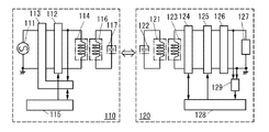
FIG. 1 is a block diagram of a power feeding device and a power reception device. FIG. 1 illustrates power transmission with an electromagnetic field using resonance of a first resonant coil in the power feeding device and a second resonant coil in the power reception device. In the block diagram in FIG. 1, circuits in the power feeding device and the power reception device are classified according to their functions and shown as independent units. Note that it is difficult to completely separate circuits in accordance with functions in an actual power feeding device and an actual power reception device. It is possible that one circuit has a plurality of functions or a plurality of circuits achieve a function corresponding to one unit.
A power feeding device 110 includes a high frequency power source 111, a first matching circuit 112, a first transmission-reception circuit 113, a first coil 114, a first control circuit 115, a first resonant coil 116, and a first resonant capacitor 117.
A power reception device 120 includes a second resonant coil 121, a second resonant capacitor 122, a second coil 123, a second transmission-reception circuit 124, a second matching circuit 125, a rectifier circuit 126, a load 127, a second control circuit 128, and a circuit 129 for detecting received power (hereinafter “received power detection circuit”).
The high frequency power source 111 is a power source circuit for outputting an alternating-current signal based on a frequency (resonant frequency of the first and the second resonant coils) for transmitting power between the power feeding device and the power reception device by a resonance method.
There is no particular limitation on the frequency (oscillation frequency) of an alternating-current signal output from the high frequency power source 111 in the power feeding device 110 in this embodiment, and the oscillation frequency can be any frequency as long as power can be transmitted from the power feeding device 110 to the power reception device 120 by a resonance method. The oscillation frequency in a resonance method can be used in the frequency range of several kilohertz to several gigahertz, for example.
The first matching circuit 112 is connected to the high frequency power source 111 through the first transmission-reception circuit 113 and connected to the first coil 114. The first matching circuit 112 includes at least one element that can adjust the impedance and is connected in series and/or in parallel with the high frequency power source 111. Note that the element that can adjust the impedance refers to a variable capacitor or a variable coil. The operation of the first matching circuit 112 is controlled by the first control circuit 115 so as to match the impedance between the high frequency power source 111 side, which is the input side, and the first coil 114 side, which is the output side.
The first transmission-reception circuit 113 is connected to the high frequency power source 111 and the first coil 114. The first transmission-reception circuit 113 has a function of generating a first wireless signal transmitted from the first coil 114 by modulating an alternating-current signal output from the high frequency power source 111, and a function of demodulating a second wireless signal received by the first coil 114. For the modulation function, a mixer circuit may be provided on the high frequency power source 111 side. The mixer circuit is a circuit that modulates the amplitude, phase, frequency, or the like of an alternating-current signal output from the high frequency power source, in accordance with an inventory signal, a data signal, or a signal for requesting the power reception device 120 to send back the power value received by the power reception device 120 to the power feeding device 110, or the like. For the demodulation function, a detector circuit, an amplifier circuit, and a rectifier circuit may be provided on the first coil 114 side.
FIG. 10A is a diagram that specifically illustrates the unit of the first transmission-reception circuit 113 in FIG. 1. In the first transmission-reception circuit 113 in FIG. 10A, a mixer circuit 501 serving as a modulation circuit is provided on the high frequency power source 111 side. Moreover, in the first transmission-reception circuit 113 in FIG. 10A, a detector circuit 502, an amplifier circuit 503, and a rectifier circuit 504 that serve as a demodulation circuit are provided on the first coil 114 side.
The first wireless signal is a wireless signal transmitted from the power feeding device 110 to the power reception device 120 and is obtained by modulation of an alternating-current signal for power feeding. The first wireless signal is a wireless signal capable of superimposing an inventory signal for requesting a response of the power reception device 120, a signal for requesting the power reception device 120 to send back the power value received by the power reception device 120 to the power feeding device 110, a data signal, or the like. In addition, the second wireless signal is a wireless signal transmitted from the power reception device 120 to the power feeding device 110 and is obtained by applying load modulation to an alternating-current signal for power feeding. The second wireless signal is a wireless signal capable of superimposing a signal for responding to an inventory signal transmitted from the power feeding device 110, a signal on the value of power received by the power reception device 120, a signal for responding to reception of a data signal by the power reception device 120, or the like. Note that the inventory signal is a signal for the power feeding device 110 to confirm the presence of the power reception device 120.
The first coil 114 is connected to the high frequency power source 111 through the first matching circuit 112 and the first transmission-reception circuit 113. It is preferable that the first coil 114 be electromagnetically coupled to the first resonant coil 116 and made by winding a wire. The first coil 114 in the power feeding device 110 has higher design flexibility than the second coil 123 in the power reception device 120 because the position of the power feeding device 110 is less restricted than the position of the power reception device 120.
The first control circuit 115 is a circuit for controlling the first matching circuit 112 in accordance with a signal that is related to the value of power received by the power reception device 120 and superimposed on the second wireless signal received by the first transmission-reception circuit 113, and for outputting a data signal that is transmitted from the first transmission-reception circuit 113 to the power reception device 120 by being superimposed on the first wireless signal. Note that as illustrated in FIG. 10A, the first control circuit 115 inputs and outputs signals to/from a storage circuit 505 that stores a plurality of data signals corresponding to values of power received by the power reception device 120.
The first resonant coil 116 is connected to the first resonant capacitor 117. It is preferable that the first resonant coil 116 be electromagnetically coupled to the first coil 114 and resonate with the second resonant coil 121, and made by winding a wire. Although there is no particular limitation on the shape of the first resonance coil 116, the first resonant coil 116 in the power feeding device 110 has higher design flexibility than the second resonant coil 121 in the power reception device 120 because the position of the power feeding device 110 is less restricted than the position of the power reception device 120. In particular, the first resonance coil 116 preferably has a high Q factor, and specifically the Q factor is preferably 100 or higher. As an example, the following signals are transmitted and received wirelessly through electromagnetic coupling between the first coil 114 and the first resonant coil 116: as the first wireless signal, an inventory signal for requesting a response of the power reception device 120, a signal for requesting the power reception device 120 to send back the power value received by the power reception device 120 to the power feeding device 110, a data signal, or the like; as the second wireless signal, a signal for responding to an inventory signal transmitted from the power feeding device 110, a signal on the value of power received by the power reception device 120, a signal for responding to reception of a data signal by the power reception device 120, or the like. Further, as an example, the following signals are transmitted and received wirelessly through resonant inductive coupling between the first resonant coil 116 and the second resonant1 coil 121: as the first wireless signal, an inventory signal for requesting a response of the power reception device 120, a signal for requesting the power reception device 120 to send back the power value received by the power reception device 120 to the power feeding device 110, a data signal, or the like; as the second wireless signal, a signal for responding to an inventory signal transmitted from the power feeding device 110, a signal on the value of power received by the power reception device 120, a signal for responding to reception of a data signal by the power reception device 120, or the like. Resonant inductive coupling is of resonance method among wireless power feeding methods, and power can be transmitted over a longer distance than electromagnetic induction with the same coil diameter.
The first resonant capacitor 117 is a capacitor provided to be paired with the first resonant coil 116 such that the desired resonant frequency is obtained. Note that the first resonant capacitor 117 does not need to be provided separately from the first resonant coil 116, and is not necessarily provided when the stray capacitance of the first resonant coil 116 is large enough to replace the first resonant capacitor 117.
The second resonant coil 121 is connected to the second resonant capacitor 122. It is preferable that the second resonant coil 121 be electromagnetically coupled to the second coil 123 and resonate with the first resonant coil 116, and made by winding a wire. Although there is no particular limitation on the shape of the second resonant coil 121, the second resonant coil 121 in the power reception device 120 is preferably designed to be smaller than the first resonant coil 116 in the power feeding device 110 because the reduction in size is demanded more strongly for the power reception device 120 than for the power feeding device 110. In particular, the second resonance coil 121 preferably has a high Q factor, and specifically the Q factor is preferably 100 or higher. As an example, the following signals are transmitted and received wirelessly through electromagnetic coupling between the second coil 123 and the second resonant coil 121: as the first wireless signal, an inventory signal for requesting a response of the power reception device 120, a signal for requesting the power reception device 120 to send back the power value received by the power reception device 120 to the power feeding device 110, a data signal, or the like; as the second wireless signal, a signal for responding to an inventory signal transmitted from the power feeding device 110, a signal on the value of power received by the power reception device 120, a signal for responding to reception of a data signal by the power reception device 120, or the like.
The second coil 123 is connected to the load 127 through the second transmission-reception circuit 124, the second matching circuit 125, and the rectifier circuit 126. It is preferable that the second coil 123 be electromagnetically coupled to the second resonant coil 121 and made by winding a wire. Although there is no particular limitation on the shape of the second coil 123, the second coil 123 in the power reception device 120 is preferably designed to be smaller than the first coil 114 in the power feeding device 110 because the reduction in size is demanded more strongly for the power reception device 120 than for the power feeding device 110.
The second transmission-reception circuit 124 is connected to the load 127 and the second coil 123 through the second matching circuit 125 and the rectifier circuit 126. The second transmission-reception circuit 124 has a function of generating the second wireless signal on which a signal on the value of power received from the power feeding device 110 is superimposed, by applying load modulation to an alternating-current signal from the power feeding device 110 for power feeding; and a function of demodulating the first wireless signal received from the power feeding device 110. For the modulation function, a circuit in which a load modulator and a modulation transistor are connected in series may be provided in parallel with the transmission-reception circuit 124 on the second coil 123 side. For the demodulation function, a detector circuit, an amplifier circuit, and a rectifier circuit may be provided on the second coil 123 side.
FIG. 10B is a diagram that specifically illustrates the unit of the second transmission-reception circuit 124 in FIG. 1. In the second transmission-reception circuit 124 in FIG. 10B, a load modulator 511 and a modulation transistor 512 that serve as a modulation circuit are provided on the second coil 123 side. Moreover, in the second transmission-reception circuit 124 in FIG. 10B, a detector circuit 513, an amplifier circuit 514, and a rectifier circuit 515 that serve as a demodulation circuit are provided on the second coil 123 side.
The second matching circuit 125 is connected to the second coil 123 through the second transmission-reception circuit 124 and connected to the rectifier circuit 126. The second matching circuit 125 includes at least one element that can adjust the impedance and is connected in series and/or in parallel with the load 127. The operation of the second matching circuit 125 is controlled by the second control circuit 128 so as to match the impedance between the second coil 123 side, which is the input side, and the rectifier circuit 126 side, which is the output side.
Note that the second matching circuit 125 preferably has the same structure as the first matching circuit 112. For example, when an element connected in series with the high frequency power source 111 is a variable capacitor in the first matching circuit 112, a corresponding element in the second matching circuit 125 is preferably a variable capacitor. Without limitation to a variable capacitor, the same can be applied to a variable coil.
The rectifier circuit 126 is a circuit for rectifying an alternating-current signal received by the second coil 123 to a direct-current signal. The rectifier circuit 126 includes a diode, for example. Moreover, the rectifier circuit including a diode may be a full-wave rectifier circuit or a half-wave rectifier circuit, and may be constituted by a circuit using a diode bridge, a full-wave rectifier circuit using a transformer, or the like.
The load 127 is any element that operates by receiving power wirelessly. Examples of the load 127 are a battery and an electric motor. Specific examples thereof are an electronic device that operates with a battery, such as a mobile phone, and an electric propulsion vehicle. Note that as illustrated in FIG. 10B, a DCDC converter 516 for converting a direct-current voltage obtained by receiving the first wireless signal by the second coil 123 into a voltage used in the load 127 may be provided between the load 127 and the rectifier circuit 126 in the power reception device 120.
The second control circuit 128 is a circuit for controlling the second matching circuit 125 in accordance with data included in the first wireless signal received by the second transmission-reception circuit 124. Moreover, the second control circuit 128 is a circuit for outputting a signal on the value of power received from the power feeding device 110, from the second transmission-reception circuit 124. The signal on the value of power is transmitted as the second wireless signal, in accordance with the product of a voltage value and a current value, that is, a power value based on an alternating-current signal from the power feeding device 110. The power value is detected by the received power detection circuit 129.
The received power detection circuit 129 is a circuit for detecting transmission efficiency of power transmitted from the power feeding device 110 to the power reception device 120. For example, the received power detection circuit 129 may include an A/D converter circuit and monitor a voltage value and a current value of an alternating-current signal received by the power reception device 120 to estimate a value of power from the power feeding device 110. The voltage value obtained in the received power detection circuit 129 is converted from an analog signal into a digital signal and can be detected in the second control circuit 128.
FIGS. 2A to 2D illustrate examples of circuit configurations of the first matching circuit 112 and the second matching circuit 125. FIGS. 2A to 2D each show the configuration of a matching circuit applicable to the first matching circuit 112 and the second matching circuit 125. In FIGS. 2A to 2D, a matching circuit 200 represents each of the first matching circuit 112 and the second matching circuit 125; an input circuit 241 represents a circuit on the input side, such as the high frequency power source 111; and an output circuit 242 represents a circuit on the output side, such as the first coil 114. Moreover, a control circuit 203 represents each of the first control circuit 115 and the second control circuit 128.
FIG. 2A illustrates the matching circuit 200 that includes a variable capacitor 201 connected in parallel with the input circuit 241 and the output circuit 242, and a capacitor 202 connected in series with the input circuit 241 and the output circuit 242. The capacitance of the variable capacitor 201 is controlled by the control circuit 203. FIG. 2B illustrates the matching circuit 200 that includes the variable capacitor 201 connected in parallel with the input circuit 241 and the output circuit 242, and a variable capacitor 212 connected in series with the input circuit 241 and the output circuit 242. The capacitances of the variable capacitors 201 and 212 are controlled by the control circuit 203.
FIG. 2C illustrates the matching circuit 200 that includes a variable coil 221 connected in parallel with the input circuit 241 and the output circuit 242, and a coil 222 connected in series with the input circuit 241 and the output circuit 242. The inductance of the variable coil 221 is controlled by the control circuit 203. FIG. 2D illustrates the matching circuit 200 that includes the variable coil 221 connected in parallel with the input circuit 241 and the output circuit 242, and a variable coil 232 connected in series with the input circuit 241 and the output circuit 242. The inductances of the variable coils 221 and 232 are controlled by the control circuit 203.
Note that the first matching circuit 112 and the second matching circuit 125 preferably have the same structure. For example, when an element connected in series with the high frequency power source 111 is a variable capacitor in the first matching circuit 112, a corresponding element in the second matching circuit 125 is preferably a variable capacitor. Without limitation to a variable capacitor, the same can be applied to a variable coil.
FIGS. 2A and 2B each show the configuration of the matching circuit in which a variable capacitor is used and electrostatic capacitance is controlled by the control circuit 203. Here, specific configurations of variable capacitors will be described. FIG. 9A illustrates a configuration in which a variable capacitance diode (also referred to as a varicap diode) 601A and a capacitor 601B are included as the variable capacitor 201 in FIG. 2A. FIG. 9B illustrates a configuration in which the variable capacitance diode 601A and the capacitor 601B are included as the variable capacitors 201, and a variable capacitance diode 602A and a capacitor 602B are included as the variable capacitor 212 in FIG. 2B. The variable capacitor including the variable capacitance diode is controlled by the control circuit through a D/A converter 603. Note that the variable capacitor is not limited to using a variable capacitance diode, and can have a structure in which a plurality of capacitors connected to a switch are connected in parallel with each other and electrostatic capacitance is controlled by controlling switching of the switch. Moreover, the variable capacitor can have a structure in which a rotary variable capacitor is mechanically controlled using an electric motor or the like so that electrostatic capacitance is variable.
Note that in the configuration of the matching circuit illustrated in any of FIG. 2A to 2D, it is possible that connection is switched between a variable capacitor and a variable coil and electrostatic capacitance is controlled by the control circuit 203. FIG. 9C illustrates a configuration in which a switch 611 switches the connection between a variable capacitor 612 and a variable coil 613. By switching the switch 611 by the control circuit 203 as illustrated in FIG. 9C, the capacitance of the variable capacitor 612 and the inductance of the variable coil 613 can be switched to be controlled.
In the following description of this embodiment, a description is given of the case where the first matching circuit 112 includes a variable capacitor (Cs) connected in series with the high frequency power source 111, and a variable capacitor (Cp) connected in parallel with the high frequency power source 111; and the second matching circuit 125 includes a variable capacitor (Cs) connected in series with the load 127, and a variable capacitor (Cp) connected in parallel with the load 127.
In a resonant wireless power feeding system, the condition in which the power transmission efficiency is at the maximum varies depending on the distance between the first resonant coil 116 in the power feeding device 110 and the second resonant coil 121 in the power reception device 120. Therefore, in the structure in this embodiment, a parameter of the first matching circuit 112 and a parameter of the second matching circuit 125 are changed so that the power transmission efficiency is maximized depending on the distance between the power feeding device 110 and the power reception device 120. Note that a signal on a parameter set (composed of the parameters of the first matching circuit 112 and the second matching circuit 125 with which the power transmission efficiency is at the maximum) corresponds to the data signal described using FIG. 1.
Note that the parameter of the first matching circuit 112 refers to the impedance of the variable capacitor or the variable coil included in the first matching circuit 112. The parameter of the second matching circuit 125 refers to the impedance of the variable capacitor or the variable coil included in the second matching circuit 125. The distance between the power feeding device 110 and the power reception device 120 refers to the distance between the first resonant coil 116 and the second resonant coil 121.
Table 1 is a table where the parameters of the first matching circuit 112 and the second matching circuit 125 are set so that the power transmission efficiency is at the maximum depending on the distance between the power feeding device 110 and the power reception device 120.
TABLE 1
Distance between
Prameter of first Prameter of second power feeding device and
No. matching circuit matching circuit power reception device
0 (Cs00, Cp00) (Cs10, Cp10) D0
1 (Cs01, Cp01) (Cs11, Cp11) D1
2 (Cs02, Cp02) (Cs12, Cp12) D2
. . . .
. . . .
. . . .
j (Cs0j, Cp0j) (Cs1j, Cp1j) Dj
. . . .
. . . .
. . . .
n (Cs0n, Cp0n) (Cs1n, Cp1n) Dn
The data of the parameters set shown in Table 1 is provided to be able to be read by the first control circuit 115 or the second control circuit 128. In this specification, a description is given below assuming that the first control circuit 115 in the power feeding device 110 includes the data in Table 1.
In Table 1, the parameter of the first matching circuit 112, the parameter of the second matching circuit 125, and the distance between the power feeding device 110 and the power reception device 120 correspond to one parameter set, to which a number is given. Note that No. 0 indicates an initial state of the first matching circuit 112 and the second matching circuit 125.
FIG 3 shows the relation between distance between the power feeding device 110 and the power reception device 120 and received power. A solid line curve 301 in FIG. 3 shows the relation between distance between the power feeding device 110 and the power reception device 120 and transmission efficiency in the j-th parameter set. A dotted curve 302 in FIG 3 shows the relation between distance between the power feeding device 110 and the power reception device 120 and transmission efficiency in the (j+1)th parameter set. Note that the transmission efficiency is the power transmission efficiency between the power feeding device and the power reception device and can be represented by an S21 parameter.
For example, in the case where the parameter of the first matching circuit 112 is set to Cs0j and Cp0j and the parameter of the second matching circuit 125 is set to Cs1j and Cp1j in the j-th parameter set as shown in Table 1, the maximum power transmission efficiency is obtained when the distance between the power feeding device 110 and the power reception device 120 is Dj (see the solid line curve 301 in FIG. 3). In other words, in the case where the distance between the power feeding device 110 and the power reception device 120 is Dj, the power transmission efficiency is not maximized when the parameter of the first matching circuit 112 is not set to Cs0j and Cp0j and the parameter of the second matching circuit 125 is not set to Cs1j and Cp1j.
For example, in the case where the parameters of the first matching circuit 112 and the second matching circuit 125 are set to Cs0j, Cp0j, Cs1j, and Cp1j, the power transmission efficiency is not maximized when the distance between the power feeding device 110 and the power reception device 120 is Dj+1 (see the dotted curve 302 in FIG. 3). By setting the parameters of the first matching circuit 112 and the second matching circuit 125 to Cs0j+1, Cp0j+1, Cs1j+1, and Cp1j+1, the power transmission efficiency is at the maximum when the distance between the power feeding device 110 and the power reception device 120 is Dj+1 (see the dotted curve 302 in FIG 3).
FIG. 6 shows the actual relation between distance between the power feeding device 110 and the power reception device 120 and transmission efficiency when the parameters of the first matching circuit 112 and the second matching circuit 125 are set such that Cs ranges from 0 to 1000 pF and Cp ranges from 0 to 150 pF. In Table 2 corresponding to FIG. 6, the parameter of the first matching circuit 112, the parameter of the second matching circuit 125, and the distance with which the power transmission efficiency is at the maximum between the power feeding device 110 and the power reception device 120 are set. Note that the data in FIG. 6 corresponds to Table 2.
TABLE 2
Distance between
Prameter of first Prameter of second power feeding device and
matching circuit matching circuit power reception device
No. (pF) (pF) (mm)
1 (150, 150) (150, 150) 35
2 (200, 150) (200, 150) 50
3 (300, 100) (300, 100) 70
4 (300, 50)  (300, 50)  85
5 (300, 0)  (300, 0)  110
6 (500, 0)  (500, 0)  130
7 (1000, 0)   (1000, 0)   150
By setting the parameter set as shown in FIG. 6 and Table 2, the transmission efficiency can be maximized in accordance with the distance between the power feeding device and the power reception device. Particularly at short distance, a reduction in transmission efficiency caused by splitting of the peak of power transmission efficiency can be suppressed.
Next, a description is given of a method for supplying power in a wireless power feeding system according to one embodiment of the present invention. FIG. 4 is a flow chart showing an example of a method for supplying power in a wireless power feeding system.
The power feeding device 110 intermittently transmits an inventory signal as the first wireless signal superimposed on an alternating-current signal of the high frequency power source (see Step 401 in FIG. 4). The power feeding device 110 repeats transmission of the inventory signal until the power reception device 120 is positioned in an appropriate position and the power feeding device 110 receives the second wireless signal for responding to the inventory signal (see Step 402 in FIG. 4). When it is determined that power reception device 120 is positioned in a position where power can be transmitted thereto, the process proceeds to the next step.
Then, after the power reception device 120 is positioned in an appropriate position, the power feeding device 110 starts wireless power transmission to the power reception device 120 continuously with the use of an alternating-current signal of the high frequency power source (see Step 403 in FIG 4). Since the parameter of the first matching circuit 112 in the power feeding device 110 and the parameter of the second matching circuit 125 in the power reception device 120 are in the initial state (e.g., the 0-th parameter set in Table 1) at this time, power transmission with high transmission efficiency is not always performed at this stage. Note that in this embodiment, a description is given of the case where the number of the selected parameter set is incremented from No. 1.
Upon the start of power transmission from the power feeding device 110 to the power reception device 120, the alternating-current signal is transmitted from the first resonant coil 116 in the power feeding device 110 to the second resonant coil 121 in the power reception device 120 by resonant inductive coupling, and converted into a direct-current signal by the rectifier circuit 126 and applied to the load 127. At this time, the second control circuit 128 in the power reception device 120 detects a voltage value and a current value of a direct current signal rectified from an alternating-current signal received by the power reception device 120, using the received power detection circuit 129 in accordance with the first wireless signal that is transmitted from the power feeding device 110 and requests the power reception device 120 to send back the power value received by the power reception device 120 to the power feeding device 110 (see Step 404 in FIG. 4). The product of the voltage value and current value at this time is denoted by a power value P0. Data on the product of the voltage value and current value (the power value P0) is transmitted using the second wireless signal to the first control circuit 115 as a signal on the value of power received by the power reception device 120 from the power feeding device 110 in accordance with an instruction on the power feeding device 110. Note that data on the product of the voltage value and current value (the power value P0) may be stored once in a storage device (not shown) connected to the second control circuit 128.
Next, power is charged (or supplied) to the load 127 in the power reception device 120 in a wait state in a given period (e.g., 300 ms) (see Step 405 in FIG. 4).
Then, the first control circuit 115 determines whether to continue charging of the load 127 depending on the charging state of the load 127 (see Step 406 in FIG 4). When it is determined that charging of the load 127 is not to be continued, charging is completed by turning off the high frequency power source 111 (see Step 407 in FIG. 4). When it is determined that charging of the load 127 is to be continued, the process proceeds to the next step.
Next, the first control circuit 115 determines whether to increment or decrement (whether to select positive variation or negative variation of) the number of the parameter set (see Step 408 in FIG 4). When it is determined that the parameter set is not incremented, an instruction to decrement the number of the parameter set is output to the first matching circuit 112 and the second matching circuit 125 (see Step 410 in FIG. 4). When it is determined that the parameter set is incremented, an instruction to increment the number of the parameter set is output to the first matching circuit 112 and the second matching circuit 125 (see Step 409 in FIG. 4). In order to output such an instruction from the first control circuit 115 to the second matching circuit 125, a data signal is output to the first transmission-reception circuit 113, and the first wireless signal is transmitted from the first transmission-reception circuit 113 to the second transmission-reception circuit 124 in the power reception device 120 and then output to the second matching circuit 125 through the second control circuit 128. After receiving the first wireless signal, the power reception device 120 transmits a signal for answering the power feeding device that the power reception device 120 has received the data signal, as the second wireless signal.
Then, after the parameter set is incremented or decremented, the second control circuit 128 detects a voltage value and a current value in accordance with a signal for requesting the power reception device 120 to send back the power value received by the power reception device 120 to the power feeding device 110 by using the received power detection circuit 129 (see Step 411 in FIG. 4). The product of the voltage value and current value at this time is denoted by a power value P1. Data on the product of the voltage value and current value (the power value P1) is transmitted using the second wireless signal to the first control circuit 115 as a signal on the value of power received by the power reception device 120 from the power feeding device 110 in accordance with the instruction on the power feeding device 110 side. Data on the product of the voltage value and current value (the power value P1) may be stored once in the storage device (not shown) connected to the second control circuit 128.
Next, the first control circuit 115 determines whether the power value P1 is larger than the power value P0 (see Step 412 in FIG. 4). When the first control circuit 115 determines that the power value P1 is smaller than the power value P0, an instruction to invert a sign of the variation of the number of the parameter set is output from the first control circuit 115 to the second matching circuit 125 (see Step 414 in FIG. 4). When the first control circuit 115 determines that the power value P1 is larger than the power value P0, an instruction to keep the sign of the variation of the number of the parameter set is output to the first matching circuit 112 and the second matching circuit 125 (see Step 413 in FIG. 4). In order to output such an instruction from the first control circuit 115 to the second matching circuit 125, a data signal is output to the first transmission-reception circuit 113, and the first wireless signal is transmitted from the first transmission-reception circuit 113 to the second transmission-reception circuit 124 in the power reception device 120 and then output to the second matching circuit 125 through the second control circuit 128. After receiving the first wireless signal, the power reception device 120 transmits a signal for answering the power feeding device that the power reception device 120 has received the data signal, as the second wireless signal.
Then, the first control circuit 115 substitutes the power value P1 into the power value P0 (see Step 415 in FIG. 4). After that, the process returns to Step 405, and the subsequent steps are repeated. In other words, a series of steps from Step 405 to Step 415 is repeated until charging of the load 127 is completed.
For example, the assumption is made that a series of Steps 405 to 415 is repeated, and the first control circuit 115 obtains the product of a voltage value and a current value of the (j−1)th parameter set (P0=Wj−1), and then increments the number of the parameter set and obtains the product of a voltage value and a current value of the j-th parameter set (P1=Wj) (see Step 411 in FIG 4).
Then, the first control circuit 115 determines whether the power value P1 is larger than the power value P0 (see Step 412 in FIG 4). When the power value P1 is determined to be larger than the power value P0 (Wj>Wj−1), an instruction to keep the sign of the variation of the number of the parameter set is output from the first control circuit 115 to the first matching circuit 112 and the second matching circuit 125 (see Step 413 in FIG. 4).
Then, the power value P1 is substituted into the power value P0 in the first control circuit 115 (see Step 415 in FIG. 4), so that P0 becomes equal to Wj and the load 127 is charged for a given period (see Step 405 in FIG. 4).
Then, the first control circuit 115 determines whether to continue charging of the load 127, and when the first control circuit 115 determines that charging is continued (Step 406 in FIG. 4), the process proceeds to Step 408.
Next, the first control circuit 115 determines whether to increment or decrement (whether to select positive variation or negative variation of) the number of the parameter set (see Step 408 in FIG. 4). Here, since it is determined in Step 411 that P0<P1 is satisfied by incrementing the number of the parameter set from No. j−1 to No. j, the first control circuit 115 outputs an instruction to increment the number of the parameter set from No. j to No. j+1 to the first matching circuit 112 and the second matching circuit 125 (see Step 409 in FIG. 4).
Then, the second control circuit 128 obtains a voltage value and a current value of the (j+1)th parameter set (see Step 411 in FIG. 4). The product of the voltage value and current value at this time is represented as follows: the power value P1=Wj+1.
Next, the first control circuit 115 determines whether the power value P1 is larger than the power value P0 (see Step 412 in FIG. 4). When the power value P1 is determined to be smaller than the power value P0 (Wj<Wj+1), an instruction to invert the sign of the variation of the number of the parameter set is output to the first matching circuit 112 and the second matching circuit 125 (see Step 414 in FIG. 4).
Then, the power value P1 is substituted into the power value P0 in the first control circuit 115 (Step 415 in FIG. 4), so that P0 becomes equal to Wj+1 and the load 127 is charged for a given period (Step 405 in FIG 4).
FIG. 5 shows the relation between the above-described parameter set numbers and transmission efficiency. As shown in FIG. 5, the transmission efficiency is at the maximum in the j-th parameter set, in which case power can be efficiently supplied from the power feeding device 110 to the power reception device 120. By successively incrementing and decrementing the number of the parameter set between j−1 and j+1 repeatedly until charging of the load 127 is completed, the load 127 can be efficiently charged.
In addition, even if the distance between the power feeding device 110 and the power reception device 120 is changed while the load 127 is charged, the parameter set can be kept shifting until charging of the load 127 is completed, whereby the load 127 can be efficiently charged.
By employing the power feeding method shown in FIG. 4, the wireless power feeding system in FIG. 1 can provide high power transmission efficiency between the power feeding device 110 and the power reception device 120 without dynamically controlling the oscillation frequency in accordance with the positional relation between the power feeding device and the power reception device.
This embodiment can be implemented in appropriate combination with the structures described in another embodiment.
(Embodiment 2)
In this embodiment, applications of the wireless power feeding system described in Embodiment 1 will be described. Examples of applications of the wireless power feeding system according to one embodiment of the present invention are portable electronic devices, such as a digital video camera, a portable information terminal (e.g., a mobile computer, a mobile phone, a portable game machine, and an e-book reader), and an image reproducing device including a recording medium (specifically a digital versatile disc (DVD)). In addition, an electric propulsion vehicle that is powered by electric power, such as an electric car, can be given. Examples will be described below with reference to drawings.
FIG. 7A illustrates an example of an application of the wireless power feeding system to a mobile phone and a portable information terminal. A power feeding device 701, a mobile phone 702A including a power reception device 703A, and a mobile phone 702B including a power reception device 703B are shown. The wireless power feeding system described in Embodiment 1 can be applied between the power feeding device 701 and the power reception device 703A and between the power feeding device 701 and the power reception device 703B.
For example, the power feeding device 701 can have the configuration of the power feeding device 110 in Embodiment 1, and the power reception devices 703A and 703B can have the configuration of the power reception device 120 in Embodiment 1.
The use of the wireless power feeding system according to one embodiment of the present invention can increase power transmission efficiency in accordance with the positional relation between the power feeding device 701 and the power reception device 703A and between the power feeding device 701 and the power reception device 703B. Consequently, the power feeding device 701 can efficiently supply power to the power reception devices 703A and 703B.
FIG. 7B illustrates an example of an application of the wireless power feeding system to an electric car which is an electric propulsion vehicle. A power feeding device 711 and an electric car 712 including a power reception device 713 are shown. The wireless power feeding system in Embodiment 1 can be applied between the power feeding device 711 and the power reception device 713.
For example, the power feeding device 711 can have the configuration of the power feeding device 110 in Embodiment 1, and the power reception device 713 can have the configuration of the power reception device 120 in Embodiment 1.
The use of the wireless power feeding system according to one embodiment of the present invention can increase power transmission efficiency in accordance with the positional relation between the power feeding device 711 and the power reception device 713. Consequently, the power feeding device 711 can efficiently supply power to the power reception device 713.
As described above, the wireless power feeding system described in Embodiment 1 can be used for any object that is driven with power.
This embodiment can be implemented in appropriate combination with the structures described in the other embodiment.
This application is based on Japanese Patent Application Ser. No. 2011-009685 filed with Japan Patent Office on Jan. 20, 2011, the entire contents of which are hereby incorporated by reference.

Claims (18)

What is claimed is:
1. A wireless power feeding device comprising:
a high frequency power source configured to output an alternating-current signal;
a first resonant coil configured to resonate with a second resonant coil of a wireless power reception device;
a coil electromagnetically coupled to the first resonant coil;
a transmission-reception circuit configured to generate a first wireless signal and demodulate a second wireless signal from the wireless power reception device;
a matching circuit configured to match impedance between the high frequency power source and the coil in accordance with a power value of the second wireless signal, the power value being detected by the wireless power reception device; and
a control circuit configured to generate a data signal of the first wireless signal in accordance with the power value of the second wireless signal, the data signal including parameters of the matching circuit.
2. The wireless power feeding device according to claim 1, wherein the transmission-reception circuit includes a modulation circuit configured to modulate the alternating-current signal output from the high frequency power source.
3. The wireless power feeding device according to claim 1, wherein the matching circuit includes a variable capacitor whose capacitance is controlled by the control circuit.
4. The wireless power feeding device according to claim 1, wherein the matching circuit includes a variable coil whose inductance is controlled by the control circuit.
5. The wireless power feeding device according to claim 1, wherein the control circuit comprises a memory circuit which stores the parameters of the matching circuit.
6. A wireless power reception device for receiving power signals from a wireless power feeding device having a first resonant coil, the device comprising:
a rectifier circuit;
a second resonant coil configured to resonate with the first resonant coil of the wireless power feeding device;
a coil electromagnetically coupled to the second resonant coil;
a transmission-reception circuit configured to demodulate a first wireless signal from the wireless power feeding device and generate a second wireless signal;
a matching circuit configured to match impedance between the rectifier circuit and the coil in accordance with a data signal of the first wireless signal, the data signal including parameters of the matching circuit; and
a control circuit configured to generate a data of the second wireless signal including a power value received from the wireless power feeding device.
7. The wireless power reception device according to claim 6, wherein the transmission-reception circuit includes a load modulator configured to apply load modulation to an alternating-current signal output from the wireless power feeding device.
8. The wireless power reception device according to claim 6, wherein the matching circuit includes a variable capacitor whose capacitance is controlled by the control circuit.
9. The wireless power reception device according to claim 6, wherein the matching circuit includes a variable coil whose inductance is controlled by the control circuit.
10. he wireless power reception device according to claim 6, further comprising a received power detection circuit configured to detect the power value received by the wireless power reception device.
11. A wireless power feeding system comprising:
a wireless power feeding device comprising:
a high frequency power source configured to output an alternating-current signal;
a first resonant coil configured to resonate with a second resonant coil;
a first coil electromagnetically coupled to the first resonant coil;
a first transmission-reception circuit configured to generate a first wireless signal and demodulate a second wireless signal;
a first matching circuit configured to match impedance between the high frequency power source and the first coil in accordance with a power value of the second wireless signal, the power value being detected by a wireless power reception device; and
a first control circuit configured to generate a data signal of the first wireless signal in accordance with the power value of the second wireless signal, the data signal including parameters of the first matching circuit, and
the wireless power reception device comprising:
the second resonant coil configured to resonate with the first resonant coil;
a second coil electromagnetically coupled to the second resonant coil;
a rectifier circuit;
a second transmission-reception circuit configured to generate the second wireless signal and demodulate the first wireless signal;
a second matching circuit configured to match impedance between the rectifier circuit and the second coil in accordance with the data signal of the first wireless signal; and
a second control circuit configured to generate the second wireless signal including the power value.
12. The wireless power feeding system according to claim 11, wherein the first transmission-reception circuit includes a modulation circuit configured to modulate an alternating-current signal output from the high frequency power source.
13. The wireless power feeding system according to claim 11,
wherein the second transmission-reception circuit includes a load modulator configured to apply load modulation to an alternating-current signal output from the wireless power feeding device.
14. The wireless power feeding system according to claim 11, wherein a configuration of the first matching circuit is the same as a configuration of the second matching circuit.
15. The wireless power feeding system according to claim 14, wherein the first matching circuit includes a variable capacitor whose capacitance is controlled by the first control circuit, and the second matching circuit includes a variable capacitor whose capacitance is controlled by the second control circuit.
16. The wireless power feeding system according to claim 14, wherein the first matching circuit includes a variable coil whose inductance is controlled by the first control circuit, and the second matching circuit includes a variable coil whose inductance is controlled by the second control circuit.
17. The wireless power feeding system according to claim 11, wherein the first control circuit comprises a memory circuit which stores the parameters of the first matching circuit and the second matching circuit.
18. The wireless power feeding system according to claim 11, further comprising a received power detection circuit configured to detect the power value received by the wireless power reception device.
US13/352,383 2011-01-20 2012-01-18 Power feeding device and wireless power feeding system Active 2033-09-30 US9024482B2 (en)

Priority Applications (2)

Application Number Priority Date Filing Date Title
US14/680,169 US9837977B2 (en) 2011-01-20 2015-04-07 Power feeding device and wireless power feeding system
US15/825,405 US10491183B2 (en) 2011-01-20 2017-11-29 Power feeding device and wireless power feeding system

Applications Claiming Priority (2)

Application Number Priority Date Filing Date Title
JP2011009685 2011-01-20
JP2011-009685 2011-01-20

Related Child Applications (1)

Application Number Title Priority Date Filing Date
US14/680,169 Continuation US9837977B2 (en) 2011-01-20 2015-04-07 Power feeding device and wireless power feeding system

Publications (2)

Publication Number Publication Date
US20120187771A1 US20120187771A1 (en) 2012-07-26
US9024482B2 true US9024482B2 (en) 2015-05-05

Family

ID=46543660

Family Applications (3)

Application Number Title Priority Date Filing Date
US13/352,383 Active 2033-09-30 US9024482B2 (en) 2011-01-20 2012-01-18 Power feeding device and wireless power feeding system
US14/680,169 Active 2032-11-30 US9837977B2 (en) 2011-01-20 2015-04-07 Power feeding device and wireless power feeding system
US15/825,405 Active 2032-04-19 US10491183B2 (en) 2011-01-20 2017-11-29 Power feeding device and wireless power feeding system

Family Applications After (2)

Application Number Title Priority Date Filing Date
US14/680,169 Active 2032-11-30 US9837977B2 (en) 2011-01-20 2015-04-07 Power feeding device and wireless power feeding system
US15/825,405 Active 2032-04-19 US10491183B2 (en) 2011-01-20 2017-11-29 Power feeding device and wireless power feeding system

Country Status (4)

Country Link
US (3) US9024482B2 (en)
JP (1) JP2012165633A (en)
KR (1) KR20120084659A (en)
TW (1) TWI539710B (en)

Cited By (6)

* Cited by examiner, † Cited by third party
Publication number Priority date Publication date Assignee Title
US20150214918A1 (en) * 2011-01-20 2015-07-30 Semiconductor Energy Laboratory Co., Ltd. Power feeding device and wireless power feeding system
US20150255990A1 (en) * 2012-11-15 2015-09-10 The Chugoku Electric Power Co., Inc. Non-contact power supply system and control method for non-contact power supply system
US20170098961A1 (en) * 2014-02-07 2017-04-06 Powerbyproxi Limited Inductive power receiver with resonant coupling regulator
US20170126071A1 (en) * 2013-08-02 2017-05-04 Integrated Deivce Technology, Inc. Multimode wireless power transmitters and related methods
CN107800201A (en) * 2016-09-05 2018-03-13 株式会社东芝 Filter circuit and wireless power induction system
US20220069635A1 (en) * 2018-12-20 2022-03-03 Guangdong Midea White Home Appliance Technology Innovation Center Co., Ltd. Wireless power transmission receiving circuit, communication method, and wireless power transmission system

Families Citing this family (23)

* Cited by examiner, † Cited by third party
Publication number Priority date Publication date Assignee Title
US9502920B2 (en) 2011-11-16 2016-11-22 Semiconductor Energy Laboratory Co., Ltd. Power receiving device, power transmission device, and power feeding system
US9246357B2 (en) * 2011-12-07 2016-01-26 Semiconductor Energy Laboratory Co., Ltd. Contactless power feeding system
US9673867B2 (en) 2012-03-14 2017-06-06 Semiconductor Energy Laboratory Co., Ltd. Power transmission device and power feeding system
US10173538B2 (en) * 2012-03-14 2019-01-08 Pioneer Corporation Wireless charging system and wireless charging transmission apparatus and method changing frequency to transmit power
JP5643270B2 (en) 2012-09-13 2014-12-17 トヨタ自動車株式会社 Vehicle and contactless power supply system
JP6119756B2 (en) 2012-09-13 2017-04-26 トヨタ自動車株式会社 Non-contact power supply system and power transmission device
KR101601352B1 (en) 2012-09-26 2016-03-08 엘지이노텍 주식회사 Apparatus for transmitting wireless power and method for controlling power thereof
JP5888201B2 (en) * 2012-10-03 2016-03-16 株式会社豊田自動織機 Power receiving device and non-contact power transmission device
JP6003573B2 (en) * 2012-11-22 2016-10-05 トヨタ自動車株式会社 Power transmission device, power reception device, vehicle including the same, and power transmission system
US20140191568A1 (en) * 2013-01-04 2014-07-10 Mojo Mobility, Inc. System and method for powering or charging multiple receivers wirelessly with a power transmitter
KR101468310B1 (en) * 2013-06-04 2014-12-02 주식회사 올레브 On-line electric vehicle
TWI513136B (en) * 2013-12-06 2015-12-11 Wireless charging system and its control method
US20150214748A1 (en) * 2014-01-24 2015-07-30 Mediatek Inc. Wireless power supply scheme capable of dynamically adjusting output power of wireless power transmitter according to voltage/current/power information of portable electronic device to be charged
US9852843B2 (en) * 2014-07-14 2017-12-26 Qualcomm Incorporated Method and apparatus for adjustable coupling for improved wireless high Q resonant power transfer
US20160064943A1 (en) * 2014-08-28 2016-03-03 Konkuk University Industrial Cooperation Corp. Controlling method and system of power transmission system
KR102207998B1 (en) * 2014-10-24 2021-01-25 엘에스전선 주식회사 Wireless power transmission apparatus and wireless power transmission system
JP5995022B1 (en) * 2015-09-10 2016-09-21 パナソニックIpマネジメント株式会社 Wireless power transmission system and power transmission device
JP2017184605A (en) * 2016-03-25 2017-10-05 古河電気工業株式会社 Power transmission and reception system and power reception apparatus
EP3493363B1 (en) * 2016-07-29 2020-07-01 Sony Semiconductor Solutions Corporation Power-supplying device
US20180083473A1 (en) * 2016-09-16 2018-03-22 Qualcomm Incorporated Variable capacitor series tuning configuration
WO2018086788A1 (en) * 2016-11-11 2018-05-17 Innogy Se Charging station, electric vehicle and system having a charging station and an electric vehicle
CN107104517A (en) * 2017-06-05 2017-08-29 三峡大学 It is a kind of to realize the MCR WPT circuits and its control method of burning voltage output
TWI741958B (en) * 2021-03-05 2021-10-01 國立陽明交通大學 Minimum power input control method

Citations (81)

* Cited by examiner, † Cited by third party
Publication number Priority date Publication date Assignee Title
US5124699A (en) 1989-06-30 1992-06-23 N.V. Netherlandsche Apparatenfabriek Nedap Electromagnetic identification system for identifying a plurality of coded responders simultaneously present in an interrogation field
JPH066272A (en) 1992-06-17 1994-01-14 Omron Corp Pulse receiving circuit of data communication equipment
US5428521A (en) 1992-10-21 1995-06-27 Alps Electric Co, Ltd. Non-contact power supply apparatus
US5652423A (en) 1994-06-21 1997-07-29 Sony Chemicals Corporation Non-contacting RF-ID card for wide voltage range input
US5790946A (en) 1993-07-15 1998-08-04 Rotzoll; Robert R. Wake up device for a communications system
JPH10285087A (en) 1997-04-10 1998-10-23 Omron Corp Data carrier and identification system
JPH1188243A (en) 1997-09-08 1999-03-30 Nippon Steel Corp Data carrier
US20020049714A1 (en) 2000-05-11 2002-04-25 Shunpei Yamazaki Communication system
JP2002259921A (en) 2001-03-02 2002-09-13 Denso Corp Id tag and receiving power control method of id tag
US6509217B1 (en) 1999-10-22 2003-01-21 Damoder Reddy Inexpensive, reliable, planar RFID tag structure and method for making same
US20030017804A1 (en) 2001-07-23 2003-01-23 Heinrich Harley Kent RFID tag having combined battery and passive power source
JP2003085506A (en) 2001-09-12 2003-03-20 Yoshikawa Rf System Kk Overvoltage preventing circuit in data carrier
US20030104848A1 (en) 2001-11-30 2003-06-05 Raj Brideglall RFID device, system and method of operation including a hybrid backscatter-based RFID tag protocol compatible with RFID, bluetooth and/or IEEE 802.11x infrastructure
US20040077383A1 (en) 2002-10-22 2004-04-22 Nokia Corporation Method and device for transponder aided wake-up of a low power radio device
US6737302B2 (en) 2001-10-31 2004-05-18 Semiconductor Energy Laboratory Co., Ltd. Manufacturing method for field-effect transistor
US20040128246A1 (en) 2002-12-27 2004-07-01 Semiconductor Energy Laboratory Co., Ltd. IC card and booking-account system using the IC card
US20040131897A1 (en) 2003-01-02 2004-07-08 Jenson Mark L. Active wireless tagging system on peel and stick substrate
US20040145454A1 (en) 2002-10-18 2004-07-29 Powell Kevin J. System and method for minimizing unwanted re-negotiation of a passive RFID tag
US6837438B1 (en) 1998-10-30 2005-01-04 Hitachi Maxell, Ltd. Non-contact information medium and communication system utilizing the same
JP2005063123A (en) 2003-08-11 2005-03-10 Fuji Electric Holdings Co Ltd Reader/writer device for non-contact card and method for automatically adjusting its antenna natural frequency, and program
US20050215119A1 (en) 2004-02-20 2005-09-29 Hitachi Maxell, Ltd. Adapter panel, electronic equipment, and cable connector identification system
US20050254183A1 (en) 2004-05-12 2005-11-17 Makota Ishida Power generation circuit using electromagnetic wave
US20060009251A1 (en) 2004-07-09 2006-01-12 Nec Corporation RF device on insulating substrate and method of manufacturing RF device
US20060044726A1 (en) 2004-09-02 2006-03-02 Mitsubishi Denki Kabushiki Kaisha Controlling circuit of power semiconductor device and controlling integrated circuit
JP2006180073A (en) 2004-12-21 2006-07-06 Okayama Prefecture Wireless ic tag
US7180421B2 (en) 2004-11-15 2007-02-20 Pahlavan Kourosh Radio frequency tag and reader with asymmetric communication bandwidth
US7209771B2 (en) 2000-12-22 2007-04-24 Terahop Networks, Inc. Battery powered wireless transceiver having LPRF component and second wake up receiver
JP2007183790A (en) 2006-01-06 2007-07-19 Hitachi Ltd Rfid device, rfid system and access control method
US20070216348A1 (en) 2006-03-15 2007-09-20 Semiconductor Energy Laboratory Co., Ltd. Electric power supply system and electric power supply system for motor vehicle
US20070229271A1 (en) 2006-03-15 2007-10-04 Semiconductor Energy Laboratory Co., Ltd. Semiconductor device
US20070229281A1 (en) 2006-03-15 2007-10-04 Semiconductor Energy Laboratory Co., Ltd. Semiconductor device
US20070229279A1 (en) 2006-03-10 2007-10-04 Shunpei Yamazaki Semiconductor device
US20070229228A1 (en) 2006-03-10 2007-10-04 Shunpei Yamazaki Semiconductor device and method for operating the same
US7301830B2 (en) 2002-03-15 2007-11-27 Nec Electronics Corporation Semiconductor memory device and semiconductor device and semiconductor memory device control method
US20070278998A1 (en) 2006-06-02 2007-12-06 Semiconductor Energy Laboratory Co., Ltd. Power storage device and mobile electronic device having the same
US20070285246A1 (en) 2006-05-31 2007-12-13 Semiconductor Energy Laboratory Co., Ltd. Semiconductor device and IC label, IC tag, and IC card having the same
US7394382B2 (en) 2004-07-01 2008-07-01 Power Id Battery-assisted backscatter RFID transponder
US20080285199A1 (en) 2004-02-13 2008-11-20 Bernd Deutschmann Circuit Arrangement and Method For Protecting an Integrated Semiconductor Circuit
US20090325651A1 (en) 2008-06-25 2009-12-31 Seiko Epson Corporation Power transmission control device, power transmission device, power reception control device, power reception device, and electronic apparatus
US20100052431A1 (en) 2008-09-02 2010-03-04 Sony Corporation Non-contact power transmission device
US7675358B2 (en) 2004-10-07 2010-03-09 Semiconductor Energy Laboratory Co., Ltd. Semiconductor device
JP2010068657A (en) 2008-09-11 2010-03-25 Yazaki Corp Wireless power transmitting device and resonance frequency adjustment method
JP2010193598A (en) 2009-02-17 2010-09-02 Nippon Soken Inc Noncontact power supply facility and noncontact power supply system
US20100244577A1 (en) 2009-03-30 2010-09-30 Fujitsu Limited Wireless power supply system and wireless power supply method
US20100244839A1 (en) 2009-03-31 2010-09-30 Fujitsu Limited Power transmitting apparatus
US20100244580A1 (en) 2009-03-31 2010-09-30 Fujitsu Limited Wireless power supply apparatus
US20100259109A1 (en) 2009-04-14 2010-10-14 Sony Corporation Power transmission device, power transmission method, power reception device, power reception method, and power transmission system
JP2010252446A (en) 2009-04-13 2010-11-04 Nippon Soken Inc Contactless power supply equipment, contactless power receiver, and contactless power supply system
JP2010252497A (en) 2009-04-14 2010-11-04 Fujitsu Ten Ltd Radio power transfer device and radio power transfer method
US20100289449A1 (en) 2007-12-19 2010-11-18 Harri Heikki Elo Wireless energy transfer
JP2010268665A (en) 2009-05-18 2010-11-25 Toyota Motor Corp Coil unit, noncontact power transmission device, noncontact power feed system, and vehicle
JP2010284066A (en) 2009-06-08 2010-12-16 Nec Tokin Corp Communication device, communication terminal and communication system
JP2010284006A (en) 2009-06-05 2010-12-16 Nec Tokin Corp Non-contact power transmission apparatus
US20110049995A1 (en) 2009-08-26 2011-03-03 Sony Corporation Noncontact electric power feeding apparatus, noncontact electric power receiving apparatus, noncontact electric power feeding method, noncontact electric power receiving method, and noncontact electric power feeding system
US7907902B2 (en) 2006-10-18 2011-03-15 Semiconductor Energy Laboratory Co., Ltd. Semiconductor device
US20110080053A1 (en) 2009-10-05 2011-04-07 Tdk Corporation Wireless power feeder and wireless power transmission system
US20110095619A1 (en) 2009-10-28 2011-04-28 Tdk Corporation Wireless power feeder, wireless power transmission system, and table and table lamp using the same
US20110101791A1 (en) 2009-10-30 2011-05-05 Tdk Corporation Wireless power feeder, wireless power transmission system, and table and table lamp using the same
JP2011120410A (en) 2009-12-04 2011-06-16 Sony Corp Power transmitter, power receiver, and power-transmission control method
US20110140537A1 (en) 2008-10-29 2011-06-16 Hitachi, Ltd. Frequency variable power transmitter and receiver in fresnel region and power transmitting system
JP2011125184A (en) 2009-12-14 2011-06-23 Toyota Motor Corp Noncontact power supply facility, noncontact power receiving apparatus, and noncontact power supply system
JP2011121456A (en) 2009-12-10 2011-06-23 Toyota Motor Corp Feeder system, vehicle, and vehicle power feeding system
JP2011130614A (en) 2009-12-18 2011-06-30 Nissan Motor Co Ltd Noncontact power supply
JP2011135717A (en) 2009-12-25 2011-07-07 Toko Inc Wireless power transmission system
US20110169337A1 (en) 2010-01-08 2011-07-14 Sony Corporation Power feed device, power receiving device, and wireless power feed system
JP2011142769A (en) 2010-01-08 2011-07-21 Toyota Central R&D Labs Inc Method and device for transmitting magnetic resonance power
US20110241440A1 (en) 2008-12-09 2011-10-06 Kabushiki Kaisha Toyota Jidoshokki Non-contact power transmission apparatus and power transmission method using a non-contact power transmission apparatus
US20110248572A1 (en) 2010-04-09 2011-10-13 Sony Corporation Power feeding apparatus, power receiving apparatus, wireless power feeding system and method for wireless transfer of power
US20110270462A1 (en) 2008-11-14 2011-11-03 Toyota Jidosha Kabushiki Kaisha Contactless power supply system and control method thereof
US8064825B2 (en) 2007-02-16 2011-11-22 Seiko Epson Corporation Power reception control device, power transmission control device, non-contact power transmission system, power reception device, power transmission device, and electronic instrument
US20110309689A1 (en) 2010-06-17 2011-12-22 Semiconductor Energy Laboratory Co., Ltd. Electric power transmitting device, electric power receiving device, and power supply method using electric power transmitting and receiving devices
US8134256B2 (en) 2008-07-15 2012-03-13 Seiko Epson Corporation Power receiving control device, power receiving device, and electronic apparatus
US8160654B2 (en) 2007-01-17 2012-04-17 Seiko Epson Corporation Power reception control device, power reception device, and electronic instrument
US8160636B2 (en) 2006-12-18 2012-04-17 Semiconductor Energy Laboratory Co., Ltd. Semiconductor device
US20120109256A1 (en) 2010-10-28 2012-05-03 Werner Meskins Magnetic induction communication system for an implantable medical device
US20120133212A1 (en) 2010-11-26 2012-05-31 Semiconductor Energy Laboratory Co., Ltd. Power transmission device and wireless power transmission system including the same
US20120161536A1 (en) 2010-12-24 2012-06-28 Semiconductor Energy Laboratory Co., Ltd. Wireless power feeding system
US8369905B2 (en) 2008-07-16 2013-02-05 Seiko Epson Corporation Power transmission control device, power transmission device, power receiving control device, power receiving device, and electronic apparatus
US8461719B2 (en) 2008-09-27 2013-06-11 Witricity Corporation Wireless energy transfer systems
US20130240877A1 (en) 2008-09-19 2013-09-19 Semiconductor Energy Laboratory Co., Ltd. Semiconductor Device and Wireless Tag Using the Same
US8716977B2 (en) * 2009-11-30 2014-05-06 Broadcom Corporation Battery with integrated wireless power receiver and/or RFID

Family Cites Families (7)

* Cited by examiner, † Cited by third party
Publication number Priority date Publication date Assignee Title
US8855554B2 (en) 2008-03-05 2014-10-07 Qualcomm Incorporated Packaging and details of a wireless power device
JP5351499B2 (en) * 2008-11-28 2013-11-27 長野日本無線株式会社 Contactless power transmission system
JP5114371B2 (en) 2008-12-09 2013-01-09 株式会社豊田自動織機 Non-contact power transmission device
JP5324901B2 (en) * 2008-12-09 2013-10-23 日立コンシューマエレクトロニクス株式会社 Non-contact power transmission system
JP5114372B2 (en) 2008-12-09 2013-01-09 株式会社豊田自動織機 Power transmission method and non-contact power transmission apparatus in non-contact power transmission apparatus
WO2011142417A1 (en) * 2010-05-14 2011-11-17 株式会社 豊田自動織機 Resonance-type non-contact power supply system, and adjustment method for matching unit during charging of resonance-type non-contact power supply system
KR20120084659A (en) * 2011-01-20 2012-07-30 가부시키가이샤 한도오따이 에네루기 켄큐쇼 Power feeding device and wireless power feeding system

Patent Citations (88)

* Cited by examiner, † Cited by third party
Publication number Priority date Publication date Assignee Title
US5124699A (en) 1989-06-30 1992-06-23 N.V. Netherlandsche Apparatenfabriek Nedap Electromagnetic identification system for identifying a plurality of coded responders simultaneously present in an interrogation field
JPH066272A (en) 1992-06-17 1994-01-14 Omron Corp Pulse receiving circuit of data communication equipment
US5428521A (en) 1992-10-21 1995-06-27 Alps Electric Co, Ltd. Non-contact power supply apparatus
US20050020321A1 (en) 1993-07-15 2005-01-27 Micron Communications, Inc. Wake up device for a communications system
US5790946A (en) 1993-07-15 1998-08-04 Rotzoll; Robert R. Wake up device for a communications system
US5652423A (en) 1994-06-21 1997-07-29 Sony Chemicals Corporation Non-contacting RF-ID card for wide voltage range input
JPH10285087A (en) 1997-04-10 1998-10-23 Omron Corp Data carrier and identification system
JPH1188243A (en) 1997-09-08 1999-03-30 Nippon Steel Corp Data carrier
US6837438B1 (en) 1998-10-30 2005-01-04 Hitachi Maxell, Ltd. Non-contact information medium and communication system utilizing the same
US6509217B1 (en) 1999-10-22 2003-01-21 Damoder Reddy Inexpensive, reliable, planar RFID tag structure and method for making same
US20020049714A1 (en) 2000-05-11 2002-04-25 Shunpei Yamazaki Communication system
US7209771B2 (en) 2000-12-22 2007-04-24 Terahop Networks, Inc. Battery powered wireless transceiver having LPRF component and second wake up receiver
JP2002259921A (en) 2001-03-02 2002-09-13 Denso Corp Id tag and receiving power control method of id tag
US20030017804A1 (en) 2001-07-23 2003-01-23 Heinrich Harley Kent RFID tag having combined battery and passive power source
JP2003085506A (en) 2001-09-12 2003-03-20 Yoshikawa Rf System Kk Overvoltage preventing circuit in data carrier
US6737302B2 (en) 2001-10-31 2004-05-18 Semiconductor Energy Laboratory Co., Ltd. Manufacturing method for field-effect transistor
US20030104848A1 (en) 2001-11-30 2003-06-05 Raj Brideglall RFID device, system and method of operation including a hybrid backscatter-based RFID tag protocol compatible with RFID, bluetooth and/or IEEE 802.11x infrastructure
US7301830B2 (en) 2002-03-15 2007-11-27 Nec Electronics Corporation Semiconductor memory device and semiconductor device and semiconductor memory device control method
US20040145454A1 (en) 2002-10-18 2004-07-29 Powell Kevin J. System and method for minimizing unwanted re-negotiation of a passive RFID tag
US20040077383A1 (en) 2002-10-22 2004-04-22 Nokia Corporation Method and device for transponder aided wake-up of a low power radio device
US20040128246A1 (en) 2002-12-27 2004-07-01 Semiconductor Energy Laboratory Co., Ltd. IC card and booking-account system using the IC card
US20040131897A1 (en) 2003-01-02 2004-07-08 Jenson Mark L. Active wireless tagging system on peel and stick substrate
JP2005063123A (en) 2003-08-11 2005-03-10 Fuji Electric Holdings Co Ltd Reader/writer device for non-contact card and method for automatically adjusting its antenna natural frequency, and program
US20080285199A1 (en) 2004-02-13 2008-11-20 Bernd Deutschmann Circuit Arrangement and Method For Protecting an Integrated Semiconductor Circuit
US20050215119A1 (en) 2004-02-20 2005-09-29 Hitachi Maxell, Ltd. Adapter panel, electronic equipment, and cable connector identification system
US20050254183A1 (en) 2004-05-12 2005-11-17 Makota Ishida Power generation circuit using electromagnetic wave
US7394382B2 (en) 2004-07-01 2008-07-01 Power Id Battery-assisted backscatter RFID transponder
US20060009251A1 (en) 2004-07-09 2006-01-12 Nec Corporation RF device on insulating substrate and method of manufacturing RF device
US20060044726A1 (en) 2004-09-02 2006-03-02 Mitsubishi Denki Kabushiki Kaisha Controlling circuit of power semiconductor device and controlling integrated circuit
US7675358B2 (en) 2004-10-07 2010-03-09 Semiconductor Energy Laboratory Co., Ltd. Semiconductor device
US7180421B2 (en) 2004-11-15 2007-02-20 Pahlavan Kourosh Radio frequency tag and reader with asymmetric communication bandwidth
JP2006180073A (en) 2004-12-21 2006-07-06 Okayama Prefecture Wireless ic tag
JP2007183790A (en) 2006-01-06 2007-07-19 Hitachi Ltd Rfid device, rfid system and access control method
US20070229279A1 (en) 2006-03-10 2007-10-04 Shunpei Yamazaki Semiconductor device
US20070229228A1 (en) 2006-03-10 2007-10-04 Shunpei Yamazaki Semiconductor device and method for operating the same
US20070229281A1 (en) 2006-03-15 2007-10-04 Semiconductor Energy Laboratory Co., Ltd. Semiconductor device
US20070229271A1 (en) 2006-03-15 2007-10-04 Semiconductor Energy Laboratory Co., Ltd. Semiconductor device
US20070216348A1 (en) 2006-03-15 2007-09-20 Semiconductor Energy Laboratory Co., Ltd. Electric power supply system and electric power supply system for motor vehicle
US20070285246A1 (en) 2006-05-31 2007-12-13 Semiconductor Energy Laboratory Co., Ltd. Semiconductor device and IC label, IC tag, and IC card having the same
US20070278998A1 (en) 2006-06-02 2007-12-06 Semiconductor Energy Laboratory Co., Ltd. Power storage device and mobile electronic device having the same
US7907902B2 (en) 2006-10-18 2011-03-15 Semiconductor Energy Laboratory Co., Ltd. Semiconductor device
US8160636B2 (en) 2006-12-18 2012-04-17 Semiconductor Energy Laboratory Co., Ltd. Semiconductor device
US8160654B2 (en) 2007-01-17 2012-04-17 Seiko Epson Corporation Power reception control device, power reception device, and electronic instrument
US8064825B2 (en) 2007-02-16 2011-11-22 Seiko Epson Corporation Power reception control device, power transmission control device, non-contact power transmission system, power reception device, power transmission device, and electronic instrument
US20100289449A1 (en) 2007-12-19 2010-11-18 Harri Heikki Elo Wireless energy transfer
US20090325651A1 (en) 2008-06-25 2009-12-31 Seiko Epson Corporation Power transmission control device, power transmission device, power reception control device, power reception device, and electronic apparatus
US8406823B2 (en) 2008-06-25 2013-03-26 Seiko Epson Corporation Power transmission control device, power transmission device, power reception control device, power reception device, and electronic apparatus
US8134256B2 (en) 2008-07-15 2012-03-13 Seiko Epson Corporation Power receiving control device, power receiving device, and electronic apparatus
US8369905B2 (en) 2008-07-16 2013-02-05 Seiko Epson Corporation Power transmission control device, power transmission device, power receiving control device, power receiving device, and electronic apparatus
US20100052431A1 (en) 2008-09-02 2010-03-04 Sony Corporation Non-contact power transmission device
JP2010068657A (en) 2008-09-11 2010-03-25 Yazaki Corp Wireless power transmitting device and resonance frequency adjustment method
US20130240877A1 (en) 2008-09-19 2013-09-19 Semiconductor Energy Laboratory Co., Ltd. Semiconductor Device and Wireless Tag Using the Same
US8461719B2 (en) 2008-09-27 2013-06-11 Witricity Corporation Wireless energy transfer systems
US8334619B2 (en) 2008-10-29 2012-12-18 Hitachi, Ltd. Frequency variable power transmitter and receiver in Fresnel region and power transmitting system
US20110140537A1 (en) 2008-10-29 2011-06-16 Hitachi, Ltd. Frequency variable power transmitter and receiver in fresnel region and power transmitting system
US20110270462A1 (en) 2008-11-14 2011-11-03 Toyota Jidosha Kabushiki Kaisha Contactless power supply system and control method thereof
US20110241440A1 (en) 2008-12-09 2011-10-06 Kabushiki Kaisha Toyota Jidoshokki Non-contact power transmission apparatus and power transmission method using a non-contact power transmission apparatus
US20120032521A1 (en) 2009-02-17 2012-02-09 Toyota Jidosha Kabushiki Kaisha Non-contact electric power feeding equipment and non-contact electric power feeding system
JP2010193598A (en) 2009-02-17 2010-09-02 Nippon Soken Inc Noncontact power supply facility and noncontact power supply system
US20100244577A1 (en) 2009-03-30 2010-09-30 Fujitsu Limited Wireless power supply system and wireless power supply method
JP2010239690A (en) 2009-03-30 2010-10-21 Fujitsu Ltd Wireless power supply system and wireless power supply method
US20100244839A1 (en) 2009-03-31 2010-09-30 Fujitsu Limited Power transmitting apparatus
US20100244580A1 (en) 2009-03-31 2010-09-30 Fujitsu Limited Wireless power supply apparatus
US8217535B2 (en) 2009-03-31 2012-07-10 Fujitsu Limited Wireless power supply apparatus
JP2010252446A (en) 2009-04-13 2010-11-04 Nippon Soken Inc Contactless power supply equipment, contactless power receiver, and contactless power supply system
US20100259109A1 (en) 2009-04-14 2010-10-14 Sony Corporation Power transmission device, power transmission method, power reception device, power reception method, and power transmission system
JP2010252468A (en) 2009-04-14 2010-11-04 Sony Corp Power transmission device and method, power receiving device and method, and power transmission system
JP2010252497A (en) 2009-04-14 2010-11-04 Fujitsu Ten Ltd Radio power transfer device and radio power transfer method
JP2010268665A (en) 2009-05-18 2010-11-25 Toyota Motor Corp Coil unit, noncontact power transmission device, noncontact power feed system, and vehicle
JP2010284006A (en) 2009-06-05 2010-12-16 Nec Tokin Corp Non-contact power transmission apparatus
JP2010284066A (en) 2009-06-08 2010-12-16 Nec Tokin Corp Communication device, communication terminal and communication system
US20110049995A1 (en) 2009-08-26 2011-03-03 Sony Corporation Noncontact electric power feeding apparatus, noncontact electric power receiving apparatus, noncontact electric power feeding method, noncontact electric power receiving method, and noncontact electric power feeding system
US20110080053A1 (en) 2009-10-05 2011-04-07 Tdk Corporation Wireless power feeder and wireless power transmission system
US20110095619A1 (en) 2009-10-28 2011-04-28 Tdk Corporation Wireless power feeder, wireless power transmission system, and table and table lamp using the same
US20110101791A1 (en) 2009-10-30 2011-05-05 Tdk Corporation Wireless power feeder, wireless power transmission system, and table and table lamp using the same
US8716977B2 (en) * 2009-11-30 2014-05-06 Broadcom Corporation Battery with integrated wireless power receiver and/or RFID
JP2011120410A (en) 2009-12-04 2011-06-16 Sony Corp Power transmitter, power receiver, and power-transmission control method
JP2011121456A (en) 2009-12-10 2011-06-23 Toyota Motor Corp Feeder system, vehicle, and vehicle power feeding system
JP2011125184A (en) 2009-12-14 2011-06-23 Toyota Motor Corp Noncontact power supply facility, noncontact power receiving apparatus, and noncontact power supply system
JP2011130614A (en) 2009-12-18 2011-06-30 Nissan Motor Co Ltd Noncontact power supply
JP2011135717A (en) 2009-12-25 2011-07-07 Toko Inc Wireless power transmission system
US20110169337A1 (en) 2010-01-08 2011-07-14 Sony Corporation Power feed device, power receiving device, and wireless power feed system
JP2011142769A (en) 2010-01-08 2011-07-21 Toyota Central R&D Labs Inc Method and device for transmitting magnetic resonance power
US20110248572A1 (en) 2010-04-09 2011-10-13 Sony Corporation Power feeding apparatus, power receiving apparatus, wireless power feeding system and method for wireless transfer of power
US20110309689A1 (en) 2010-06-17 2011-12-22 Semiconductor Energy Laboratory Co., Ltd. Electric power transmitting device, electric power receiving device, and power supply method using electric power transmitting and receiving devices
US20120109256A1 (en) 2010-10-28 2012-05-03 Werner Meskins Magnetic induction communication system for an implantable medical device
US20120133212A1 (en) 2010-11-26 2012-05-31 Semiconductor Energy Laboratory Co., Ltd. Power transmission device and wireless power transmission system including the same
US20120161536A1 (en) 2010-12-24 2012-06-28 Semiconductor Energy Laboratory Co., Ltd. Wireless power feeding system

Non-Patent Citations (1)

* Cited by examiner, † Cited by third party
Title
Kurs et al., "Wireless Power Transfer via Strongly Coupled Magnetic Resonances", Science, vol. 317, Jul. 6, 2007, pp. 83-86.

Cited By (12)

* Cited by examiner, † Cited by third party
Publication number Priority date Publication date Assignee Title
US20150214918A1 (en) * 2011-01-20 2015-07-30 Semiconductor Energy Laboratory Co., Ltd. Power feeding device and wireless power feeding system
US9837977B2 (en) * 2011-01-20 2017-12-05 Semiconductor Energy Laboratory Co., Ltd. Power feeding device and wireless power feeding system
US20180091113A1 (en) * 2011-01-20 2018-03-29 Semiconductor Energy Laboratory Co., Ltd. Power feeding device and wireless power feeding system
US10491183B2 (en) * 2011-01-20 2019-11-26 Semiconductor Energy Laboratory Co., Ltd. Power feeding device and wireless power feeding system
US20150255990A1 (en) * 2012-11-15 2015-09-10 The Chugoku Electric Power Co., Inc. Non-contact power supply system and control method for non-contact power supply system
US9711970B2 (en) * 2012-11-15 2017-07-18 The Chugoku Electric Power Co., Inc. Non-contact power supply system and control method for non-contact power supply system
US20170126071A1 (en) * 2013-08-02 2017-05-04 Integrated Deivce Technology, Inc. Multimode wireless power transmitters and related methods
US20170098961A1 (en) * 2014-02-07 2017-04-06 Powerbyproxi Limited Inductive power receiver with resonant coupling regulator
CN107800201A (en) * 2016-09-05 2018-03-13 株式会社东芝 Filter circuit and wireless power induction system
CN107800201B (en) * 2016-09-05 2020-12-22 株式会社东芝 Filter circuit and wireless power transmission system
US20220069635A1 (en) * 2018-12-20 2022-03-03 Guangdong Midea White Home Appliance Technology Innovation Center Co., Ltd. Wireless power transmission receiving circuit, communication method, and wireless power transmission system
US11909229B2 (en) * 2018-12-20 2024-02-20 Guangdong Midea White Home Appliance Technology Innovation Center Co., Ltd. Wireless power transmission receiving circuit, communication method, and wireless power transmission system

Also Published As

Publication number Publication date
TW201234736A (en) 2012-08-16
US20150214918A1 (en) 2015-07-30
US20120187771A1 (en) 2012-07-26
KR20120084659A (en) 2012-07-30
US20180091113A1 (en) 2018-03-29
TWI539710B (en) 2016-06-21
US9837977B2 (en) 2017-12-05
US10491183B2 (en) 2019-11-26
JP2012165633A (en) 2012-08-30

Similar Documents

Publication Publication Date Title
US10491183B2 (en) Power feeding device and wireless power feeding system
JP5947534B2 (en) Contactless power supply system
US10790675B2 (en) Apparatus for transmitting power wirelessly
US10069340B2 (en) Wireless power receiver for adjusting magnitude of wireless power
US10340739B2 (en) Power receiving device, power transmission device, and power feeding system
US9325205B2 (en) Method for driving power supply system
US20170093221A1 (en) Power transmission device and wireless power transmission system including the same
JP6585210B2 (en) Power receiving device
US10298064B2 (en) Power receiving unit, power feeding control method, and feed system
JP2012170315A (en) Power receiving apparatus, power supply system and power supply method
JP2018023276A (en) System and method for charging receiver devices
JP2019208313A (en) Wireless power transmission device, control circuit thereof, and wireless charging device
WO2014030689A1 (en) Non-contact power transmission device and power-receiving apparatus

Legal Events

Date Code Title Description
AS Assignment

Owner name: SEMICONDUCTOR ENERGY LABORATORY CO., LTD., JAPAN

Free format text: ASSIGNMENT OF ASSIGNORS INTEREST;ASSIGNORS:KAMATA, KOICHIRO;OKANO, SHINYA;SATO, MISAKO;AND OTHERS;SIGNING DATES FROM 20120106 TO 20120109;REEL/FRAME:027549/0118

STCF Information on status: patent grant

Free format text: PATENTED CASE

CC Certificate of correction
MAFP Maintenance fee payment

Free format text: PAYMENT OF MAINTENANCE FEE, 4TH YEAR, LARGE ENTITY (ORIGINAL EVENT CODE: M1551); ENTITY STATUS OF PATENT OWNER: LARGE ENTITY

Year of fee payment: 4

MAFP Maintenance fee payment

Free format text: PAYMENT OF MAINTENANCE FEE, 8TH YEAR, LARGE ENTITY (ORIGINAL EVENT CODE: M1552); ENTITY STATUS OF PATENT OWNER: LARGE ENTITY

Year of fee payment: 8