US9030232B2 - Isolator circuit and semiconductor device - Google Patents
Isolator circuit and semiconductor device Download PDFInfo
- Publication number
- US9030232B2 US9030232B2 US13/857,185 US201313857185A US9030232B2 US 9030232 B2 US9030232 B2 US 9030232B2 US 201313857185 A US201313857185 A US 201313857185A US 9030232 B2 US9030232 B2 US 9030232B2
- Authority
- US
- United States
- Prior art keywords
- transistor
- terminal
- circuit
- electrically connected
- layer
- Prior art date
- Legal status (The legal status is an assumption and is not a legal conclusion. Google has not performed a legal analysis and makes no representation as to the accuracy of the status listed.)
- Active, expires
Links
Images


Classifications
-
- H—ELECTRICITY
- H01—ELECTRIC ELEMENTS
- H01L—SEMICONDUCTOR DEVICES NOT COVERED BY CLASS H10
- H01L27/00—Devices consisting of a plurality of semiconductor or other solid-state components formed in or on a common substrate
- H01L27/02—Devices consisting of a plurality of semiconductor or other solid-state components formed in or on a common substrate including semiconductor components specially adapted for rectifying, oscillating, amplifying or switching and having at least one potential-jump barrier or surface barrier; including integrated passive circuit elements with at least one potential-jump barrier or surface barrier
- H01L27/04—Devices consisting of a plurality of semiconductor or other solid-state components formed in or on a common substrate including semiconductor components specially adapted for rectifying, oscillating, amplifying or switching and having at least one potential-jump barrier or surface barrier; including integrated passive circuit elements with at least one potential-jump barrier or surface barrier the substrate being a semiconductor body
- H01L27/06—Devices consisting of a plurality of semiconductor or other solid-state components formed in or on a common substrate including semiconductor components specially adapted for rectifying, oscillating, amplifying or switching and having at least one potential-jump barrier or surface barrier; including integrated passive circuit elements with at least one potential-jump barrier or surface barrier the substrate being a semiconductor body including a plurality of individual components in a non-repetitive configuration
- H01L27/0605—Devices consisting of a plurality of semiconductor or other solid-state components formed in or on a common substrate including semiconductor components specially adapted for rectifying, oscillating, amplifying or switching and having at least one potential-jump barrier or surface barrier; including integrated passive circuit elements with at least one potential-jump barrier or surface barrier the substrate being a semiconductor body including a plurality of individual components in a non-repetitive configuration integrated circuits made of compound material, e.g. AIIIBV
-
- H—ELECTRICITY
- H01—ELECTRIC ELEMENTS
- H01L—SEMICONDUCTOR DEVICES NOT COVERED BY CLASS H10
- H01L27/00—Devices consisting of a plurality of semiconductor or other solid-state components formed in or on a common substrate
- H01L27/02—Devices consisting of a plurality of semiconductor or other solid-state components formed in or on a common substrate including semiconductor components specially adapted for rectifying, oscillating, amplifying or switching and having at least one potential-jump barrier or surface barrier; including integrated passive circuit elements with at least one potential-jump barrier or surface barrier
- H01L27/04—Devices consisting of a plurality of semiconductor or other solid-state components formed in or on a common substrate including semiconductor components specially adapted for rectifying, oscillating, amplifying or switching and having at least one potential-jump barrier or surface barrier; including integrated passive circuit elements with at least one potential-jump barrier or surface barrier the substrate being a semiconductor body
- H01L27/06—Devices consisting of a plurality of semiconductor or other solid-state components formed in or on a common substrate including semiconductor components specially adapted for rectifying, oscillating, amplifying or switching and having at least one potential-jump barrier or surface barrier; including integrated passive circuit elements with at least one potential-jump barrier or surface barrier the substrate being a semiconductor body including a plurality of individual components in a non-repetitive configuration
- H01L27/0688—Integrated circuits having a three-dimensional layout
-
- H—ELECTRICITY
- H01—ELECTRIC ELEMENTS
- H01L—SEMICONDUCTOR DEVICES NOT COVERED BY CLASS H10
- H01L27/00—Devices consisting of a plurality of semiconductor or other solid-state components formed in or on a common substrate
- H01L27/02—Devices consisting of a plurality of semiconductor or other solid-state components formed in or on a common substrate including semiconductor components specially adapted for rectifying, oscillating, amplifying or switching and having at least one potential-jump barrier or surface barrier; including integrated passive circuit elements with at least one potential-jump barrier or surface barrier
- H01L27/12—Devices consisting of a plurality of semiconductor or other solid-state components formed in or on a common substrate including semiconductor components specially adapted for rectifying, oscillating, amplifying or switching and having at least one potential-jump barrier or surface barrier; including integrated passive circuit elements with at least one potential-jump barrier or surface barrier the substrate being other than a semiconductor body, e.g. an insulating body
- H01L27/1203—Devices consisting of a plurality of semiconductor or other solid-state components formed in or on a common substrate including semiconductor components specially adapted for rectifying, oscillating, amplifying or switching and having at least one potential-jump barrier or surface barrier; including integrated passive circuit elements with at least one potential-jump barrier or surface barrier the substrate being other than a semiconductor body, e.g. an insulating body the substrate comprising an insulating body on a semiconductor body, e.g. SOI
Definitions
- a semiconductor device refers to a semiconductor element itself or a device including a semiconductor element.
- a semiconductor element a thin film transistor is given, for example. Therefore, the semiconductor device includes a liquid crystal display device, a memory device, and the like.
- a portable semiconductor device such as a mobile computer has been rapidly spread.
- a portable semiconductor device includes a power storage portion and operates using power fed from the power storage portion, the charge/discharge capacity of the power storage portion is finite. Accordingly, there is a demand for reducing power consumption as much as possible.
- An object of one embodiment of the present invention is to provide a novel isolator circuit capable of two-way electrical disconnection and a semiconductor device including the isolator circuit.
- One embodiment of the present invention is an isolator circuit in which two one-way isolator circuits each capable of one-way electrical disconnection are combined.
- Another embodiment of the present invention is a semiconductor device in which a logic circuit and a signal line are electrically connected to each other through an isolator circuit having the above structure.
- Another embodiment of the present invention is a semiconductor device including a plurality of isolator circuits each having the above structure and a plurality of logic circuits. One of the plurality of logic circuits is electrically connected to a signal line through one of the plurality of isolator circuits.
- a novel isolator circuit capable of two-way electrical disconnection and a semiconductor device including the isolator circuit can be provided.
- FIGS. 1A and 1B are views illustrating one structural example and one application example, respectively, of an isolator circuit which is one embodiment of the present invention
- FIGS. 2A to 2C are views illustrating structural examples of an isolator circuit which is one embodiment of the present invention.
- FIG. 3 is a view illustrating a specific structure of part of the isolator circuit in FIGS. 1A and 1B ;
- FIG. 4 is a view illustrating a semiconductor device which is one embodiment of the present invention.
- FIG. 5 is a view illustrating a first logic circuit 402 and a first isolator circuit 404 in FIG. 4 ;
- FIGS. 6A and 6B are views each illustrating an example of a cross section of a transistor which can be applied to one embodiment of the present invention.
- FIG. 7 is a view illustrating an example of a cross section of a transistor which can be applied to one embodiment of the present invention.
- FIGS. 1A and 1B an isolator circuit which is one embodiment of the present invention will be described with reference to FIGS. 1A and 1B , FIGS. 2A to 2C , FIG. 3 , FIG. 4 , and FIG. 5 .
- FIG. 1A illustrates a circuit 100 functioning as an isolator circuit which is one embodiment of the present invention.
- the circuit 100 illustrated in FIG. 1A is electrically connected to a first terminal 102 and a second terminal 104 .
- the first terminal 102 and the second terminal 104 are an input terminal and an output terminal, respectively; however, without limitation thereto, the first terminal 102 and the second terminal 104 may be an output terminal and an input terminal, respectively.
- the first terminal 102 is electrically connected to one of a source and a drain of a first transistor 106
- the other of the source and the drain of the first transistor 106 is electrically connected to an input terminal of a first buffer 108
- an output terminal of the first buffer 108 is electrically connected to the second terminal 104 .
- first terminal 102 is electrically connected to an output terminal of a second buffer 110
- an input terminal of the second buffer 110 is electrically connected to one of a source and a drain of a second transistor 112
- the other of the source and the drain of the second transistor 112 is electrically connected to the second terminal 104 .
- a gate of the first transistor 106 is electrically connected to a terminal 114 .
- a potential of the terminal 114 can be controlled. When the terminal 114 has a high potential (H), the first transistor 106 is on, and when the terminal 114 has a low potential (L), the first transistor 106 is off.
- a terminal 116 is electrically connected to the first buffer 108 .
- a potential of the terminal 116 can be controlled.
- the terminal 116 corresponds to a third terminal 310 in FIG. 3 which is described later.
- a terminal 118 is electrically connected to the second buffer 110 .
- a potential of the terminal 118 can be controlled.
- the terminal 118 corresponds to the third terminal 310 in FIG. 3 which is described later, as is the case with the terminal 116 .
- a gate of the second transistor 112 is electrically connected to a terminal 120 .
- a potential of the terminal 120 can be controlled.
- the terminal 120 has a high potential (H)
- the second transistor 112 is on
- the terminal 120 has a low potential (L)
- the second transistor 112 is off.
- any transistor can be used as each of the first transistor 106 and the second transistor 112 as long as it has small off-state current.
- the off-state current per micrometer of channel width is 10 aA (1 ⁇ 10 ⁇ 17 A) or lower, preferably 1 aA (1 ⁇ 10 ⁇ 18 A) or lower, further preferably 10 zA (1 ⁇ 10 ⁇ 20 A) or lower, still further preferably 1 zA (1 ⁇ 10 ⁇ 21 A) or lower, most preferably 100 yA (1 ⁇ 10 ⁇ 22 A) or lower.
- any structure can be employed for each of the first buffer 108 and the second buffer 110 as long as it is a structure in which a data holding portion can be formed between the transistor and the buffer, and in which data in the data holding portion can be output to the first terminal 102 or the second terminal 104 when the terminal 116 or the terminal 118 has a high potential (H).
- Such a structure can be realized by a combination of an inverter and a clocked inverter, for example. Note that a specific structure of the first buffer 108 and the second buffer 110 will be described later with reference to FIG. 3 .
- the data holding portions are each denoted by a thick line in FIG. 1A .
- FIG. 1B is a view illustrating an application example of the circuit 100 in FIG. 1A .
- the circuit 100 is provided between a first logic circuit 150 and a second logic circuit 152 .
- the terminal 114 , the terminal 118 , and the terminal 120 are each set to have a low potential (L), and the terminal 116 is set to have a high potential (H).
- L low potential
- H high potential
- FIG. 2A illustrates a circuit 200 as an example of an isolator circuit which is another embodiment of the present invention.
- the circuit 200 in FIG. 2A is electrically connected to a first terminal 202 and a second terminal 204 .
- the first terminal 202 is electrically connected to an input terminal of a first transmission gate 206
- an output terminal of the first transmission gate 206 is electrically connected to the second terminal 204 and one of a source and a drain of a first transistor 208 .
- first terminal 202 is electrically connected to one of a source and a drain of a second transistor 210 and an output terminal of a second transmission gate 212 , and an input terminal of the second transmission gate 212 is electrically connected to the second terminal 204 .
- each of the first transmission gate 206 and the second transmission gate 212 may be reversed.
- FIG. 2B illustrates an example of a specific structure of the first transmission gate 206 or the second transmission gate 212 .
- the first transmission gate 206 is electrically connected to a first control terminal 214 and a second control terminal 216 . Potentials of the first control terminal 214 and the second control terminal 216 can be controlled.
- first control terminal 214 has a high potential (H) and the second control terminal 216 has a low potential (L)
- H high potential
- L low potential
- the p-channel transistor and the n-channel transistor in the first transmission gate 206 are both turned on.
- a gate of the first transistor 208 is electrically connected to a terminal 218 .
- the other of the source and the drain of the first transistor 208 is electrically connected to a terminal 220 .
- a potential of the terminal 218 can be controlled. When the terminal 218 has a high potential (H), the first transistor 208 is on, and when the terminal 218 has a low potential (L), the first transistor 208 is off.
- the terminal 220 is electrically connected to a low-potential power supply line Vss.
- a gate of the second transistor 210 is electrically connected to a terminal 222 .
- the other of the source and the drain of the second transistor 210 is electrically connected to a terminal 224 .
- a potential of the terminal 222 can be controlled. When the terminal 222 has a high potential (H), the second transistor 210 is turned on, and when the terminal 222 has a low potential (L), the second transistor 210 is turned off.
- the terminal 224 is electrically connected to the low-potential power supply line Vss.
- the second transmission gate 212 is electrically connected to a first control terminal 226 and a second control terminal 228 . Potentials of the first control terminal 226 and the second control terminal 228 can be controlled.
- first control terminal 226 has a high potential (H) and the second control terminal 228 has a low potential (L)
- a p-channel transistor and an n-channel transistor in the second transmission gate 212 are both turned off.
- the p-channel transistor and the n-channel transistor in the second transmission gate 212 are both turned on.
- FIG. 2C illustrates a circuit 250 as an example of an isolator circuit which is another embodiment of the present invention.
- the circuit 250 in FIG. 2C is electrically connected to a first terminal 252 and a second terminal 254 .
- the first terminal 252 is electrically connected to one of input terminals of a first AND circuit 256
- an output terminal of the first AND circuit 256 is electrically connected to the second terminal 254 .
- the other of the input terminals of the first AND circuit 256 is electrically connected to a terminal 260 .
- first terminal 252 is electrically connected to an output terminal of a second AND circuit 258 .
- One of input terminals of the second AND circuit 258 is electrically connected to the second terminal 254 , and the other of the input terminals of the second AND circuit 258 is electrically connected to a terminal 262 .
- Potentials of the terminal 260 and the terminal 262 can be controlled.
- the terminal 260 has a high potential (H) and a signal is supplied from the first terminal 252 (the first terminal 252 has a high potential (H))
- the signal is output from the output terminal of the first AND circuit 256 .
- the terminal 260 has a low potential (L)
- the signal is not output from the output terminal of the first AND circuit 256 .
- signal transmission can be controlled.
- a data holding portion is not provided, and accordingly, data is erased when power is turned off. Therefore, a data holding portion needs to be provided additionally for enabling data hold.
- a data holding portion is provided in an isolator circuit, so that an isolator circuit where data is not erased even when power is turned off can be obtained without the need for additional provision of a data holding portion.
- the logic circuit to which the data is input can continue the processing even when power feeding to the logic circuit which has output the data is stopped.
- An object of one embodiment of the present invention which is illustrated in FIG. 1A is to provide a semiconductor device in which a logic circuit (a circuit to which data is input) can continue processing even when another logic circuit which outputs the data which is input to the logic circuit (the circuit to which the data is input) is turned off.
- An object of one embodiment of the present invention which is illustrated in FIG. 1A is to provide a semiconductor device in which even when data which is input to a logic circuit is output from another logic circuit, the latter logic circuit which outputs the data which is input to the former logic circuit can be turned off.
- An object of one embodiment of the present invention which is illustrated in FIG. 1A is to achieve the above-described objects without the need for additional provision of a data holding portion.
- a data holding portion is provided in an isolator circuit without the need for additional provision of a data holding portion outside, and data which is input to a logic circuit which outputs the data is stored in the data holding portion.
- FIG. 1A One embodiment of the present invention which is illustrated in FIG. 1A is an isolator circuit including a first terminal, a second terminal, a first transistor, a second transistor, a first buffer, and a second buffer.
- the first terminal is electrically connected to one of a source and a drain of the first transistor and an output terminal of the second buffer.
- the other of the source and the drain of the first transistor is electrically connected to an input terminal of the first buffer.
- An input terminal of the second buffer is electrically connected to one of a source and a drain of the second transistor.
- the second terminal is electrically connected to an output terminal of the first buffer and the other of the source and the drain of the second transistor.
- the off-state current per micrometer of channel width in each of the first transistor and the second transistor is 10 aA (1 ⁇ 10 ⁇ 17 A) or lower.
- an inverter and a clocked inverter are preferably provided.
- a channel is preferably formed in an oxide semiconductor layer.
- data which is output from a logic circuit (a circuit which outputs data) and input to another logic circuit (a circuit to which the data is input) is held in the data holding portion provided in the isolator circuit, and thus the latter logic circuit (the circuit to which the data is input) can continue processing even when the former logic circuit (the circuit which outputs the data) is turned off.
- FIG. 1A data which is output from a logic circuit (a circuit which outputs data) and input to another logic circuit (a circuit to which the data is input) is held in the data holding portion provided in the isolator circuit, and thus the former logic circuit (the circuit which outputs the data) can be turned off even in the case where the latter logic circuit (the circuit to which the data is input) continues processing.
- FIG. 3 illustrates a circuit 300 as an example of the first buffer 108 and the second buffer 110 in FIG. 1A having a specific configuration.
- the circuit 300 in FIG. 3 is electrically connected to a first terminal 302 and a second terminal 304 .
- the circuit 300 in FIG. 3 includes an inverter circuit including a first transistor 306 and a second transistor 308 ; and a clocked inverter circuit including a third transistor 314 , a fourth transistor 316 , a fifth transistor 318 , and a sixth transistor 320 .
- the first terminal 302 is electrically connected to a gate of the first transistor 306 and a gate of the second transistor 308 .
- One of a source and a drain of the first transistor 306 is electrically connected to a high-potential power supply line Vdd.
- the other of the source and the drain of the first transistor 306 is electrically connected to one of a source and a drain of the second transistor 308 .
- the other of the source and the drain of the second transistor 308 is electrically connected to the low-potential power supply line Vss.
- the third terminal 310 is electrically connected to an input terminal of a NOT circuit 312 and a gate of the sixth transistor 320 .
- An output terminal of the NOT circuit 312 is electrically connected to a gate of the third transistor 314 .
- a gate of the fourth transistor 316 and a gate of the fifth transistor 318 are electrically connected to the other of the source and the drain of the first transistor 306 and the one of the source and the drain of the second transistor 308 .
- One of a source and a drain of the third transistor 314 is electrically connected to the high-potential power supply line Vdd.
- the other of the source and the drain of the third transistor 314 is electrically connected to one of a source and a drain of the fourth transistor 316 .
- the other of the source and the drain of the fourth transistor 316 is electrically connected to one of a source and a drain of the fifth transistor 318 .
- the other of the source and the drain of the fifth transistor 318 is electrically connected to one of a source and a drain of the sixth transistor 320 .
- the other of the source and the drain of the sixth transistor 320 is electrically connected to the low-potential power supply line Vss.
- the other of the source and the drain of the fourth transistor 316 and the one of the source and the drain of the fifth transistor 318 are electrically connected to the second terminal 304 .
- first transistor 306 , the third transistor 314 , and the fourth transistor 316 are p-channel transistors
- the second transistor 308 , the fifth transistor 318 , and the sixth transistor 320 are n-channel transistors.
- the first terminal 302 is an input terminal of the circuit 300 .
- the second terminal 304 is an output terminal of the circuit 300 .
- a potential of the third terminal 310 can be controlled, and the third terminal 310 corresponds to the terminal 116 or the terminal 118 in FIG. 1A .
- the isolator circuit which is one embodiment of the present invention described above can be applied to a semiconductor device.
- a semiconductor device including the isolator circuit which is one embodiment of the present invention will be described below.
- FIG. 4 illustrates a semiconductor device 400 as a semiconductor device which is one embodiment of the present invention.
- the semiconductor device 400 includes a first logic circuit 402 , a second logic circuit 406 , and a third logic circuit 410 .
- a first isolator circuit 404 , a second isolator circuit 408 , and a third isolator circuit 412 are electrically connected to the first logic circuit 402 , the second logic circuit 406 , and the third logic circuit 410 , respectively.
- the first isolator circuit 404 , the second isolator circuit 408 , and the third isolator circuit 412 each correspond to the circuit 100 in FIG. 1A .
- first logic circuit 402 the second logic circuit 406 , and the third logic circuit 410 are logic circuits.
- the first logic circuit 402 , the second logic circuit 406 , and the third logic circuit 410 which are included in the semiconductor device 400 are electrically connected to a signal line 414 , which is shared among these logic circuits, through the first isolator circuit 404 , the second isolator circuit 408 , and the third isolator circuit 412 , respectively.
- the first logic circuit 402 , the second logic circuit 406 , and the third logic circuit 410 share one signal line.
- FIG. 5 focuses on the first logic circuit 402 and the first isolator circuit 404 in the structure.
- the first isolator circuit 404 corresponds to the circuit 100 in FIG. 1A ; therefore, the same reference numerals as those in FIG. 1A are used.
- a first terminal 502 and a second terminal 504 correspond to the first terminal 102 and the second terminal 104 in FIG. 1A , respectively.
- the terminal 114 and the terminal 116 are each set to have a high potential (H), and the terminal 118 and the terminal 120 are each set to have a low potential (L).
- the signal line 500 corresponds to the signal line 414 in FIG. 4 .
- the terminal 114 and the terminal 116 are each set to have a low potential (L), and the terminal 118 and the terminal 120 are each set to have a high potential (H).
- the terminal 114 , the terminal 118 , and the terminal 120 are each set to have a low potential (L), and the terminal 116 is set to have a high potential (H).
- the necessary data is output to the signal line 500 even when the first logic circuit 402 is turned off.
- the first logic circuit 402 can be turned off even in the case where the data from the first logic circuit 402 needs to be output to the signal line 500 .
- the terminal 116 is set to have a low potential (L) in the case where the data from the first logic circuit 402 does not need to be output to the signal line 500 .
- the terminals 114 , 116 , 118 , and 120 are each set to have a low potential (L) before the logic circuit in an on state is turned off. In this manner, the first logic circuit 402 in an off state can be electrically disconnected from the logic circuit in an on state.
- a semiconductor device which is one embodiment of the present invention includes isolator circuits which are each one embodiment of the present invention.
- the use of the isolator circuits enables each of logic circuits included in the semiconductor device to be turned off, so that power consumption can be reduced effectively.
- the logic circuit in an off state and the logic circuit in an on state are electrically disconnected from each other, whereby reverse current to a power supply line or an increase in consumption current due to an intermediate potential can be prevented, and the logic circuit in an on state can perform processing using an output result that is obtained from the logic circuit in an off state just before the logic circuit is turned off.
- a transistor illustrated in FIG. 6A includes a semiconductor layer 604 , an insulating layer 610 , a conductive layer 612 , an insulating layer 614 a , an insulating layer 614 b , an insulating layer 616 , a conductive layer 618 a , a conductive layer 618 b , and an insulating layer 620 .
- the semiconductor layer 604 is provided over an element formation layer 600 with an insulating layer 602 placed therebetween. Note that there is no limitation thereto, and the semiconductor layer 604 may be directly provided over the element formation layer 600 .
- the semiconductor layer 604 includes a region 606 a and a region 606 b to which dopant is added, and further includes a channel formation region 608 between the region 606 a and the region 606 b.
- the insulating layer 610 is provided over part of the semiconductor layer 604 .
- the conductive layer 612 is provided to overlap with the semiconductor layer 604 with the insulating layer 610 placed therebetween.
- the insulating layer 614 a and the insulating layer 614 b are each a sidewall insulating layer which is provided in contact with a side surface of the conductive layer 612 .
- the insulating layer 616 is provided over the conductive layer 612 .
- the conductive layer 618 a and the conductive layer 618 b are provided in contact with the region 606 a and the region 606 b , respectively.
- the conductive layer 618 a and the conductive layer 618 b are also provided in contact with a side surface of the insulating layer 614 a and a side surface of the insulating layer 614 b , respectively.
- the insulating layer 620 is provided over the conductive layer 618 a and the conductive layer 618 b.
- the conductive layer 618 a , the conductive layer 618 b , and the insulating layer 620 are formed by CMP treatment, for example.
- a transistor illustrated in FIG. 6B includes a conductive layer 652 , an insulating layer 654 , an insulating layer 656 , a semiconductor layer 658 , a conductive layer 660 a , a conductive layer 660 b , a conductive layer 662 a , a conductive layer 662 b , and an insulating layer 664 .
- the conductive layer 652 is provided over an element formation layer 650 .
- the insulating layer 654 is provided over the element formation layer 650 .
- Surfaces of the conductive layer 652 and the insulating layer 654 are preferably flat.
- the conductive layer 652 and the insulating layer 654 are formed by CMP treatment, for example.
- the insulating layer 656 is provided over the conductive layer 652 and the insulating layer 654 .
- the semiconductor layer 658 is provided to overlap with the conductive layer 652 with the insulating layer 656 placed therebetween.
- the conductive layer 660 a and the conductive layer 660 b are provided in contact with the semiconductor layer 658 .
- the distance between the conductive layer 660 a and the conductive layer 660 b which corresponds to a channel length of the transistor, is preferably shorter than 50 nm.
- the distance between the conductive layers 660 a and 660 b can be made shorter than 50 nm in such a manner that, for example, part of a conductive film is etched using a resist mask formed by electron beam exposure.
- the distance between the conductive layers 660 a and 660 b is preferably shorter than a distance between the conductive layers 662 a and 662 b , as illustrated in FIG. 6B .
- the conductive layer 662 a is provided on and in contact with part of the conductive layer 660 a
- the conductive layer 662 b is provided on and in contact with part of the conductive layer 660 b .
- the electrical resistivity per unit area of the conductive layers 662 a and 662 b is preferably lower than that of the conductive layers 660 a and 660 b.
- the insulating layer 664 is provided so as to cover the semiconductor layer 658 .
- each of the components illustrated in FIGS. 6A and 6B will be described. Note that the components each have either a single-layer structure or a stacked-layer structure in which a plurality of layers are stacked.
- the insulating layer 602 is a base layer.
- the insulating layer 602 can be formed using, for example, a material such as silicon oxide, silicon nitride, silicon oxynitride, silicon nitride oxide, aluminum oxide, aluminum nitride, aluminum oxynitride, aluminum nitride oxide, or hafnium oxide.
- the insulating layer 654 may be formed using the same material as the insulating layer 602 .
- Each of the semiconductor layers 604 and 658 functions as a layer in which a channel of the transistor is formed (a channel formation layer).
- a channel formation layer the semiconductor layer 604 in FIG. 6A and the semiconductor layer 658 in FIG. 6B will be described.
- an oxide semiconductor layer can be used as each of the semiconductor layers 604 and 658 .
- a structure of an oxide semiconductor layer is described below.
- An oxide semiconductor layer is classified roughly into a single-crystal oxide semiconductor layer and a non-single-crystal oxide semiconductor layer.
- the non-single-crystal oxide semiconductor layer includes any of an amorphous oxide semiconductor layer, a microcrystalline oxide semiconductor layer, a polycrystalline oxide semiconductor layer, a c-axis aligned crystalline oxide semiconductor (CAAC-OS) layer, and the like.
- the amorphous oxide semiconductor layer has disordered atomic arrangement and no crystalline component.
- a typical example thereof is an oxide semiconductor layer in which no crystal part exists even in a microscopic region, and the whole of the layer is amorphous.
- the microcrystalline oxide semiconductor layer includes a microcrystal (also referred to as nanocrystal) with a size greater than or equal to 1 nm and less than 10 nm, for example.
- the microcrystalline oxide semiconductor layer has a higher degree of atomic order than the amorphous oxide semiconductor layer.
- the density of defect states of the microcrystalline oxide semiconductor layer is lower than that of the amorphous oxide semiconductor layer.
- the CAAC-OS layer is one of oxide semiconductor layers including a plurality of crystal parts, and most of each crystal part fits inside a cube whose one side is less than 100 nm. Thus, there is a case where a crystal part included in the CAAC-OS layer fits a cube whose one side is less than 10 nm, less than 5 nm, or less than 3 nm.
- the density of defect states of the CAAC-OS layer is lower than that of the microcrystalline oxide semiconductor layer.
- the CAAC-OS layer is described in detail below.
- TEM transmission electron microscope
- metal atoms are arranged in a layered manner in the crystal parts.
- Each metal atom layer has a morphology reflected by a surface over which the CAAC-OS layer is formed (hereinafter, a surface over which the CAAC-OS layer is formed is referred to as a formation surface) or a top surface of the CAAC-OS layer, and is arranged in parallel to the formation surface or the top surface of the CAAC-OS layer.
- metal atoms are arranged in a triangular or hexagonal configuration in the crystal parts.
- plane TEM image there is no regularity of arrangement of metal atoms between different crystal parts.
- a term “parallel” indicates that the angle formed between two straight lines is greater than or equal to ⁇ 10° and less than or equal to 10°, and accordingly also includes the case where the angle is greater than or equal to ⁇ 5° and less than or equal to 5°.
- a term “perpendicular” indicates that the angle formed between two straight lines is greater than or equal to 80° and less than or equal to 100°, and accordingly includes the case where the angle is greater than or equal to 85° and less than or equal to 95°.
- the trigonal and rhombohedral crystal systems are included in the hexagonal crystal system.
- a CAAC-OS layer is subjected to structural analysis with an X-ray diffraction (XRD) apparatus.
- XRD X-ray diffraction
- each metal atom layer arranged in a layered manner observed in the cross-sectional TEM image corresponds to a plane parallel to the a-b plane of the crystal.
- the crystal part is formed concurrently with formation of the CAAC-OS layer or is formed through crystallization treatment such as heat treatment.
- the c-axis of the crystal is aligned in a direction parallel to a normal vector of a formation surface or a normal vector of a top surface.
- the c-axis might not be necessarily parallel to a normal vector of a formation surface or a normal vector of a top surface of the CAAC-OS layer.
- the degree of crystallinity in the CAAC-OS layer is not necessarily uniform.
- the degree of the crystallinity in the vicinity of the top surface is higher than that in the vicinity of the formation surface in some cases.
- the crystallinity in a region to which the impurity is added is changed, and the degree of crystallinity in the CAAC-OS layer varies depends on regions.
- a peak of 2 ⁇ may also be observed at around 36°, in addition to the peak of 2 ⁇ at around 31°.
- the peak of 2 ⁇ at around 36° is derived from the (311) plane of a ZnGa 2 O 4 crystal; such a peak indicates that a ZnGa 2 O 4 crystal is included in part of the CAAC-OS layer including the InGaZnO 4 crystal. It is preferable that in the CAAC-OS layer, a peak of 2 ⁇ appear at around 31° and a peak of 2 ⁇ do not appear at around 36°.
- the transistor In a transistor using the CAAC-OS layer, change in electric characteristics due to irradiation with visible light or ultraviolet light is small. Thus, the transistor has high reliability.
- an oxide semiconductor layer may be a stacked layer including two or more layers of an amorphous oxide semiconductor layer, a microcrystalline oxide semiconductor layer, and a CAAC-OS layer, for example.
- oxide semiconductor examples include a metal oxide containing zinc and at least one of indium and gallium, and the metal oxide in which gallium is partly or entirely replaced with another metal element.
- an In-based metal oxide As the metal oxide, an In-based metal oxide, a Zn-based metal oxide, an In—Zn-based metal oxide, or an In—Ga—Zn-based metal oxide can be used, for example.
- metal oxide including another metal element instead of part or all of gallium in the In—Ga—Zn-based metal oxide may be used.
- a metal element that is capable of combining with more oxygen atoms than gallium can be used, and one or more elements of titanium, zirconium, hafnium, germanium, and tin can be used, for instance.
- one or more elements of lanthanum, cerium, praseodymium, neodymium, samarium, europium, gadolinium, terbium, dysprosium, holmium, erbium, thulium, ytterbium, and lutetium may be used. These metal elements function as a stabilizer.
- the amount of such a metal element added is determined so that the metal oxide can function as a semiconductor.
- a metal element that is capable of combining with more oxygen atoms than gallium is used and oxygen is supplied to a metal oxide, oxygen defects in the metal oxide can be reduced.
- an In—Sn—Zn-based metal oxide is obtained.
- titanium is replaced with part of gallium contained in the In—Ga—Zn-based metal oxide, an In—Ti—Ga—Zn-based metal oxide is obtained.
- the oxide semiconductor layer It is preferable to remove impurities such as hydrogen, water, a hydroxyl group, and a hydride (also referred to as a hydrogen compound) from an oxide semiconductor layer by dehydration or dehydrogenation and supply oxygen to the oxide semiconductor layer in the case where the oxide semiconductor layer is used as the semiconductor layers 604 and 658 , because the oxide semiconductor layer can be highly purified.
- impurities such as hydrogen, water, a hydroxyl group, and a hydride (also referred to as a hydrogen compound) from an oxide semiconductor layer by dehydration or dehydrogenation and supply oxygen to the oxide semiconductor layer in the case where the oxide semiconductor layer is used as the semiconductor layers 604 and 658 , because the oxide semiconductor layer can be highly purified.
- a layer containing oxygen is formed as the layer in contact with the oxide semiconductor layer, and heat treatment is performed; thus, the oxide semiconductor layer can be highly purified.
- the oxide semiconductor layer that has just been deposited is preferably supersaturated with oxygen so that the proportion of oxygen is higher than that in the stoichiometric composition.
- the deposition is preferably performed under the condition where the proportion of oxygen in a deposition gas is large, in particular, in an oxygen atmosphere (oxygen gas: 100%).
- an insulating layer containing excess oxygen e.g., a SiO x layer where x>2
- the oxide semiconductor layer e.g., the insulating layers 602 , 610 , 656 , and 664 ).
- the insulating layer containing excess oxygen is formed to contain much oxygen by adjusting the deposition condition in a CVD method or a sputtering method.
- oxygen is added by ion implantation, ion doping, or plasma treatment.
- oxygen may be added to the oxide semiconductor layer.
- An entrapment vacuum pump is preferably used in a sputtering apparatus which is used for formation of the oxide semiconductor layer because it is preferable that as little moisture as possible remain in a deposition chamber. Further, the sputtering apparatus may be provided with a cold trap.
- the oxide semiconductor layer is preferably subjected to heat treatment at a substrate temperature higher than or equal to 350° C. and lower than the strain point of a substrate, preferably at a substrate temperature ranging from 350° C. to 450° C.
- Heat treatment may be further performed in a later step.
- a heat treatment apparatus there is no particular limitation on a heat treatment apparatus to be used here, and an electric furnace or an a rapid thermal annealing (RTA) apparatus such as a gas rapid thermal annealing (GRTA) apparatus or a lamp rapid thermal annealing (LRTA) apparatus may be used. Heat treatment may be performed more than once.
- RTA rapid thermal annealing
- GRTA gas rapid thermal annealing
- LRTA lamp rapid thermal annealing
- a high-purity oxygen gas, a high-purity N 2 O gas, or ultra-dry air (having a dew point of ⁇ 40° C. or lower, preferably ⁇ 60° C. or lower) is preferably introduced in the furnace where the heat treatment has been performed while the heating temperature is being maintained or being decreased.
- the oxygen gas or the N 2 O gas do not contain water, hydrogen, and the like.
- the purity of the oxygen gas or the N 2 O gas which is introduced into the heat treatment apparatus is preferably 6N or higher, more preferably 7N or higher. That is, the impurity concentration of the oxygen gas or the N 2 O gas is 1 ppm or lower, preferably 0.1 ppm or lower.
- oxygen is supplied to the oxide semiconductor layer, and oxygen vacancies in the oxide semiconductor layer can be reduced.
- introduction of a high-purity oxygen gas, a high-purity N 2 O gas, or ultra-dry air may be performed at the time of the above heat treatment.
- the hydrogen concentration of the highly purified oxide semiconductor layer is 5 ⁇ 10 19 atoms/cm 3 or lower, preferably 5 ⁇ 10 18 atoms/cm 3 or lower, more preferably 5 ⁇ 10 17 atoms/cm 3 or lower.
- the carrier density of the oxide semiconductor layer can be lower than 1 ⁇ 10 14 /cm 3 , preferably lower than 1 ⁇ 10 12 /cm 3 , further preferably lower than 1 ⁇ 10 11 /cm 3 .
- Such a low carrier density can reduce the off-state current of the field-effect transistor per micrometer of channel width to 1 ⁇ 10 ⁇ 19 A (100 zA) or lower, preferably 1 ⁇ 10 ⁇ 22 A (100 yA) or lower.
- the dopant contained in the regions 606 a and 606 b it is possible to use, for example, one or more elements selected from Group 13 elements (e.g., boron) in the periodic table, Group 15 elements (e.g., nitrogen, phosphorus, and arsenic) in the periodic table, and rare gas elements (e.g., helium, argon, and xenon).
- Group 13 elements e.g., boron
- Group 15 elements e.g., nitrogen, phosphorus, and arsenic
- rare gas elements e.g., helium, argon, and xenon.
- the insulating layers 610 and 656 each function as a gate insulating layer of the transistor.
- Each of the insulating layers 610 and 656 can be, for example, a layer containing a material such as silicon oxide, silicon nitride, silicon oxynitride, silicon nitride oxide, aluminum oxide, aluminum nitride, aluminum oxynitride, aluminum nitride oxide, or hafnium oxide.
- the conductive layers 612 and 652 each function as a gate of the transistor.
- Each of the conductive layers 612 and 652 can be, for example, a layer containing a metal material such as molybdenum, titanium, chromium, tantalum, magnesium, silver, tungsten, aluminum, copper, neodymium, or scandium.
- Each of the insulating layers 614 a , 614 b , and 616 can be, for example, a layer containing a material such as silicon oxide, silicon nitride, silicon oxynitride, silicon nitride oxide, aluminum oxide, aluminum nitride, aluminum oxynitride, aluminum nitride oxide, or hafnium oxide.
- the conductive layers 618 a and 618 b , the conductive layers 660 a and 660 b , and the conductive layers 662 a and 662 b each function as a source or a drain of the transistor.
- Each of the conductive layers 618 a and 618 b , the conductive layers 660 a and 660 b , and the conductive layers 662 a and 662 b can be, for example, a layer containing a conductive material such as molybdenum, titanium, chromium, tantalum, magnesium, silver, tungsten, aluminum, copper, neodymium, scandium, or ruthenium.
- the insulating layers 620 and 664 each function as a protection layer.
- Each of the insulating layers 620 and 664 can be, for example, a layer including a material such as silicon oxide, silicon nitride, silicon oxynitride, silicon nitride oxide, aluminum oxide, aluminum nitride, aluminum oxynitride, aluminum nitride oxide, or hafnium oxide.
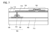
- FIG. 7 is a schematic cross-sectional view illustrating an example of a structure of a semiconductor device in this embodiment.
- the semiconductor device illustrated in FIG. 7 includes a transistor 700 including a single crystal silicon layer 708 that is a channel formation layer, and a transistor 702 that is stacked over the transistor 700 with insulating layers 712 , 714 , and 716 placed therebetween and has the structure illustrated in FIG. 6A . Further, an insulating layer 720 is provided in contact with the transistor 702 .
- the single crystal silicon layer 708 is provided over a substrate 704 with an insulating layer 706 (also referred to as BOX layer) placed therebetween.
- the transistor 700 may be configured using a semiconductor region surrounded by a buried insulating region in a single crystal semiconductor substrate, instead of using the substrate 704 , the insulating layer 706 , and the single crystal silicon layer 708 .
- the insulating layer 712 functions as a protection layer.
- the insulating layer 714 functions as both a protection layer and a planarization layer.
- the insulating layer 716 functions as a base layer.
- Each of the insulating layers 712 , 714 , and 716 can be a layer containing a material similar to that of the insulating layer 602 .
- a conductive layer 718 functioning as a source or a drain of the transistor 702 is connected to a conductive layer 710 functioning as a gate of the transistor 700 .
- the conductive layer 718 and the conductive layer 710 may be connected to each other through a plurality of conductive layers.
- the use of the transistor with small off-state current as the transistor 702 can increase the data retention time of a memory cell.
- the transistor 700 can be included in a logic circuit (including a volatile memory circuit) of a CPU, a signal processing circuit, or the like. In this case, high operation speed can be achieved.
- the transistor 702 illustrated in FIG. 7 corresponds to the first transistor 106 in FIG. 1A which is described in Embodiment 1.
- the transistor 700 illustrated in FIG. 7 corresponds to the first transistor 306 or the second transistor 308 in FIG. 3 which is described in Embodiment 1. Accordingly, the conductive layer 718 in FIG. 7 functions as a data holding portion.
- a transistor with small off-state current can be manufactured as described in this embodiment, a semiconductor device which is one embodiment of the present invention can be achieved.
- the transistor with small off-state current is not limited to the transistor described in this embodiment. There is no particular limitation on the structure of the transistor with small off-state current as long as the transistor has small off-state current that allows the data holding portion to hold data for a necessary period of time.
Landscapes
- Engineering & Computer Science (AREA)
- Power Engineering (AREA)
- Physics & Mathematics (AREA)
- Condensed Matter Physics & Semiconductors (AREA)
- General Physics & Mathematics (AREA)
- Computer Hardware Design (AREA)
- Microelectronics & Electronic Packaging (AREA)
- Thin Film Transistor (AREA)
- Static Random-Access Memory (AREA)
- Electronic Switches (AREA)
Abstract
Description
- [Patent Document 1] Japanese Published Patent Application No. 2008-172230
Claims (20)
Applications Claiming Priority (2)
| Application Number | Priority Date | Filing Date | Title |
|---|---|---|---|
| JP2012091727 | 2012-04-13 | ||
| JP2012-091727 | 2012-04-13 |
Publications (2)
| Publication Number | Publication Date |
|---|---|
| US20130270551A1 US20130270551A1 (en) | 2013-10-17 |
| US9030232B2 true US9030232B2 (en) | 2015-05-12 |
Family
ID=49324273
Family Applications (1)
| Application Number | Title | Priority Date | Filing Date |
|---|---|---|---|
| US13/857,185 Active 2033-08-03 US9030232B2 (en) | 2012-04-13 | 2013-04-05 | Isolator circuit and semiconductor device |
Country Status (2)
| Country | Link |
|---|---|
| US (1) | US9030232B2 (en) |
| JP (1) | JP6214904B2 (en) |
Families Citing this family (8)
| Publication number | Priority date | Publication date | Assignee | Title |
|---|---|---|---|---|
| JP6396671B2 (en) | 2013-04-26 | 2018-09-26 | 株式会社半導体エネルギー研究所 | Semiconductor device |
| JP6106024B2 (en) * | 2013-05-21 | 2017-03-29 | 株式会社ジャパンディスプレイ | Thin film transistor manufacturing method and thin film transistor |
| DE102016207737A1 (en) * | 2015-05-11 | 2016-11-17 | Semiconductor Energy Laboratory Co., Ltd. | Semiconductor device, method for manufacturing the semiconductor device, tire and moving object |
| US9627275B1 (en) * | 2015-10-30 | 2017-04-18 | Taiwan Semiconductor Manufacturing Company Ltd. | Hybrid semiconductor structure on a common substrate |
| CN109478883A (en) | 2016-07-19 | 2019-03-15 | 株式会社半导体能源研究所 | Semiconductor device |
| US10120470B2 (en) | 2016-07-22 | 2018-11-06 | Semiconductor Energy Laboratory Co., Ltd. | Semiconductor device, display device and electronic device |
| WO2018122658A1 (en) | 2016-12-27 | 2018-07-05 | Semiconductor Energy Laboratory Co., Ltd. | Semiconductor device |
| US11538804B2 (en) * | 2019-01-09 | 2022-12-27 | Intel Corporation | Stacked integration of III-N transistors and thin-film transistors |
Citations (107)
| Publication number | Priority date | Publication date | Assignee | Title |
|---|---|---|---|---|
| JPS60198861A (en) | 1984-03-23 | 1985-10-08 | Fujitsu Ltd | Thin film transistor |
| JPS63210024A (en) | 1987-02-24 | 1988-08-31 | Natl Inst For Res In Inorg Mater | Compound having laminar structure of hexagonal crystal system expressed by ingazn5o8 and its production |
| JPS63210023A (en) | 1987-02-24 | 1988-08-31 | Natl Inst For Res In Inorg Mater | Compound having laminar structure of hexagonal crystal system expressed by ingazn4o7 and its production |
| JPS63210022A (en) | 1987-02-24 | 1988-08-31 | Natl Inst For Res In Inorg Mater | Compound having laminar structure of hexagonal crystal system expressed by ingazn3o6 and its production |
| JPS63215519A (en) | 1987-02-27 | 1988-09-08 | Natl Inst For Res In Inorg Mater | Chemical compound of ingazn6o9 with hexagonal system layer structure |
| JPS63239117A (en) | 1987-01-28 | 1988-10-05 | Natl Inst For Res In Inorg Mater | Compound having lamellar structure of hexagonal system expressed in ingazn2o5 and its production |
| JPS63265818A (en) | 1987-04-22 | 1988-11-02 | Natl Inst For Res In Inorg Mater | Compound having hexagonal laminar structure expressed by ingazn7o10 and its production |
| JPH05251705A (en) | 1992-03-04 | 1993-09-28 | Fuji Xerox Co Ltd | Thin-film transistor |
| JPH08264794A (en) | 1995-03-27 | 1996-10-11 | Res Dev Corp Of Japan | Metal oxide semiconductor device forming a pn junction with a thin film transistor of metal oxide semiconductor of copper suboxide and manufacture thereof |
| US5731856A (en) | 1995-12-30 | 1998-03-24 | Samsung Electronics Co., Ltd. | Methods for forming liquid crystal displays including thin film transistors and gate pads having a particular structure |
| US5744864A (en) | 1995-08-03 | 1998-04-28 | U.S. Philips Corporation | Semiconductor device having a transparent switching element |
| JP2000044236A (en) | 1998-07-24 | 2000-02-15 | Hoya Corp | Article having transparent conductive oxide thin film and its production |
| JP2000150900A (en) | 1998-11-17 | 2000-05-30 | Japan Science & Technology Corp | Transistor and semiconductor device |
| US6294274B1 (en) | 1998-11-16 | 2001-09-25 | Tdk Corporation | Oxide thin film |
| US20010046027A1 (en) | 1999-09-03 | 2001-11-29 | Ya-Hsiang Tai | Liquid crystal display having stripe-shaped common electrodes formed above plate-shaped pixel electrodes |
| JP2002076356A (en) | 2000-09-01 | 2002-03-15 | Japan Science & Technology Corp | Semiconductor device |
| US20020056838A1 (en) | 2000-11-15 | 2002-05-16 | Matsushita Electric Industrial Co., Ltd. | Thin film transistor array, method of producing the same, and display panel using the same |
| US20020132454A1 (en) | 2001-03-19 | 2002-09-19 | Fuji Xerox Co., Ltd. | Method of forming crystalline semiconductor thin film on base substrate, lamination formed with crystalline semiconductor thin film and color filter |
| JP2002289859A (en) | 2001-03-23 | 2002-10-04 | Minolta Co Ltd | Thin-film transistor |
| JP2003086808A (en) | 2001-09-10 | 2003-03-20 | Masashi Kawasaki | Thin film transistor and matrix display |
| JP2003086000A (en) | 2001-09-10 | 2003-03-20 | Sharp Corp | Semiconductor memory and its test method |
| US20030189401A1 (en) | 2002-03-26 | 2003-10-09 | International Manufacturing And Engineering Services Co., Ltd. | Organic electroluminescent device |
| US20030218222A1 (en) | 2002-05-21 | 2003-11-27 | The State Of Oregon Acting And Through The Oregon State Board Of Higher Education On Behalf Of | Transistor structures and methods for making the same |
| US20040038446A1 (en) | 2002-03-15 | 2004-02-26 | Sanyo Electric Co., Ltd.- | Method for forming ZnO film, method for forming ZnO semiconductor layer, method for fabricating semiconductor device, and semiconductor device |
| JP2004103957A (en) | 2002-09-11 | 2004-04-02 | Japan Science & Technology Corp | Transparent thin film field effect type transistor using homologous thin film as active layer |
| US20040127038A1 (en) | 2002-10-11 | 2004-07-01 | Carcia Peter Francis | Transparent oxide semiconductor thin film transistors |
| JP2004273614A (en) | 2003-03-06 | 2004-09-30 | Sharp Corp | Semiconductor device and its fabricating process |
| JP2004273732A (en) | 2003-03-07 | 2004-09-30 | Sharp Corp | Active matrix substrate and its producing process |
| WO2004114391A1 (en) | 2003-06-20 | 2004-12-29 | Sharp Kabushiki Kaisha | Semiconductor device, its manufacturing method, and electronic device |
| US20050017302A1 (en) | 2003-07-25 | 2005-01-27 | Randy Hoffman | Transistor including a deposited channel region having a doped portion |
| US20050199959A1 (en) | 2004-03-12 | 2005-09-15 | Chiang Hai Q. | Semiconductor device |
| US20060043377A1 (en) | 2004-03-12 | 2006-03-02 | Hewlett-Packard Development Company, L.P. | Semiconductor device |
| US20060091793A1 (en) | 2004-11-02 | 2006-05-04 | 3M Innovative Properties Company | Methods and displays utilizing integrated zinc oxide row and column drivers in conjunction with organic light emitting diodes |
| US20060110867A1 (en) | 2004-11-10 | 2006-05-25 | Canon Kabushiki Kaisha | Field effect transistor manufacturing method |
| US20060108636A1 (en) | 2004-11-10 | 2006-05-25 | Canon Kabushiki Kaisha | Amorphous oxide and field effect transistor |
| US20060108529A1 (en) | 2004-11-10 | 2006-05-25 | Canon Kabushiki Kaisha | Sensor and image pickup device |
| US20060113536A1 (en) | 2004-11-10 | 2006-06-01 | Canon Kabushiki Kaisha | Display |
| US20060113539A1 (en) | 2004-11-10 | 2006-06-01 | Canon Kabushiki Kaisha | Field effect transistor |
| US20060113565A1 (en) | 2004-11-10 | 2006-06-01 | Canon Kabushiki Kaisha | Electric elements and circuits utilizing amorphous oxides |
| US20060113549A1 (en) | 2004-11-10 | 2006-06-01 | Canon Kabushiki Kaisha | Light-emitting device |
| US7061014B2 (en) | 2001-11-05 | 2006-06-13 | Japan Science And Technology Agency | Natural-superlattice homologous single crystal thin film, method for preparation thereof, and device using said single crystal thin film |
| US20060170111A1 (en) | 2005-01-28 | 2006-08-03 | Semiconductor Energy Laboratory Co., Ltd. | Semiconductor device, electronic device, and method of manufacturing semiconductor device |
| US20060169973A1 (en) | 2005-01-28 | 2006-08-03 | Semiconductor Energy Laboratory Co., Ltd. | Semiconductor device, electronic device, and method of manufacturing semiconductor device |
| US20060197092A1 (en) | 2005-03-03 | 2006-09-07 | Randy Hoffman | System and method for forming conductive material on a substrate |
| US7105868B2 (en) | 2002-06-24 | 2006-09-12 | Cermet, Inc. | High-electron mobility transistor with zinc oxide |
| US20060208977A1 (en) | 2005-03-18 | 2006-09-21 | Semiconductor Energy Laboratory Co., Ltd. | Semiconductor device, and display device, driving method and electronic apparatus thereof |
| US20060228974A1 (en) | 2005-03-31 | 2006-10-12 | Theiss Steven D | Methods of making displays |
| US20060231882A1 (en) | 2005-03-28 | 2006-10-19 | Il-Doo Kim | Low voltage flexible organic/transparent transistor for selective gas sensing, photodetecting and CMOS device applications |
| US20060238135A1 (en) | 2005-04-20 | 2006-10-26 | Semiconductor Energy Laboratory Co., Ltd. | Semiconductor device and display device |
| US20060284172A1 (en) | 2005-06-10 | 2006-12-21 | Casio Computer Co., Ltd. | Thin film transistor having oxide semiconductor layer and manufacturing method thereof |
| US20060284171A1 (en) | 2005-06-16 | 2006-12-21 | Levy David H | Methods of making thin film transistors comprising zinc-oxide-based semiconductor materials and transistors made thereby |
| EP1737044A1 (en) | 2004-03-12 | 2006-12-27 | Japan Science and Technology Agency | Amorphous oxide and thin film transistor |
| US20060292777A1 (en) | 2005-06-27 | 2006-12-28 | 3M Innovative Properties Company | Method for making electronic devices using metal oxide nanoparticles |
| US20070024187A1 (en) | 2005-07-28 | 2007-02-01 | Shin Hyun S | Organic light emitting display (OLED) and its method of fabrication |
| US20070046191A1 (en) | 2005-08-23 | 2007-03-01 | Canon Kabushiki Kaisha | Organic electroluminescent display device and manufacturing method thereof |
| US20070054507A1 (en) | 2005-09-06 | 2007-03-08 | Canon Kabushiki Kaisha | Method of fabricating oxide semiconductor device |
| US20070052025A1 (en) | 2005-09-06 | 2007-03-08 | Canon Kabushiki Kaisha | Oxide semiconductor thin film transistor and method of manufacturing the same |
| US20070090365A1 (en) | 2005-10-20 | 2007-04-26 | Canon Kabushiki Kaisha | Field-effect transistor including transparent oxide and light-shielding member, and display utilizing the transistor |
| US7211825B2 (en) | 2004-06-14 | 2007-05-01 | Yi-Chi Shih | Indium oxide-based thin film transistors and circuits |
| US20070108446A1 (en) | 2005-11-15 | 2007-05-17 | Semiconductor Energy Laboratory Co., Ltd. | Semiconductor device and manufacturing method thereof |
| US20070152217A1 (en) | 2005-12-29 | 2007-07-05 | Chih-Ming Lai | Pixel structure of active matrix organic light-emitting diode and method for fabricating the same |
| US20070172591A1 (en) | 2006-01-21 | 2007-07-26 | Samsung Electronics Co., Ltd. | METHOD OF FABRICATING ZnO FILM AND THIN FILM TRANSISTOR ADOPTING THE ZnO FILM |
| US20070187760A1 (en) | 2006-02-02 | 2007-08-16 | Kochi Industrial Promotion Center | Thin film transistor including low resistance conductive thin films and manufacturing method thereof |
| US20070187678A1 (en) | 2006-02-15 | 2007-08-16 | Kochi Industrial Promotion Center | Semiconductor device including active layer made of zinc oxide with controlled orientations and manufacturing method thereof |
| US20070252928A1 (en) | 2006-04-28 | 2007-11-01 | Toppan Printing Co., Ltd. | Structure, transmission type liquid crystal display, reflection type display and manufacturing method thereof |
| US7297977B2 (en) | 2004-03-12 | 2007-11-20 | Hewlett-Packard Development Company, L.P. | Semiconductor device |
| US20070272922A1 (en) | 2006-04-11 | 2007-11-29 | Samsung Electronics Co. Ltd. | ZnO thin film transistor and method of forming the same |
| US20070287296A1 (en) | 2006-06-13 | 2007-12-13 | Canon Kabushiki Kaisha | Dry etching method for oxide semiconductor film |
| US20080006877A1 (en) | 2004-09-17 | 2008-01-10 | Peter Mardilovich | Method of Forming a Solution Processed Device |
| US7323356B2 (en) | 2002-02-21 | 2008-01-29 | Japan Science And Technology Agency | LnCuO(S,Se,Te)monocrystalline thin film, its manufacturing method, and optical device or electronic device using the monocrystalline thin film |
| US20080038882A1 (en) | 2006-08-09 | 2008-02-14 | Kazushige Takechi | Thin-film device and method of fabricating the same |
| US20080038929A1 (en) | 2006-08-09 | 2008-02-14 | Canon Kabushiki Kaisha | Method of dry etching oxide semiconductor film |
| US20080050595A1 (en) | 2006-01-11 | 2008-02-28 | Murata Manufacturing Co., Ltd. | Transparent conductive film and method for manufacturing the same |
| US20080073653A1 (en) | 2006-09-27 | 2008-03-27 | Canon Kabushiki Kaisha | Semiconductor apparatus and method of manufacturing the same |
| US20080083950A1 (en) | 2006-10-10 | 2008-04-10 | Alfred I-Tsung Pan | Fused nanocrystal thin film semiconductor and method |
| US20080106191A1 (en) | 2006-09-27 | 2008-05-08 | Seiko Epson Corporation | Electronic device, organic electroluminescence device, and organic thin film semiconductor device |
| US20080128689A1 (en) | 2006-11-29 | 2008-06-05 | Je-Hun Lee | Flat panel displays comprising a thin-film transistor having a semiconductive oxide in its channel and methods of fabricating the same for use in flat panel displays |
| US20080129195A1 (en) | 2006-12-04 | 2008-06-05 | Toppan Printing Co., Ltd. | Color el display and method for producing the same |
| US7385224B2 (en) | 2004-09-02 | 2008-06-10 | Casio Computer Co., Ltd. | Thin film transistor having an etching protection film and manufacturing method thereof |
| US20080166834A1 (en) | 2007-01-05 | 2008-07-10 | Samsung Electronics Co., Ltd. | Thin film etching method |
| US7402506B2 (en) | 2005-06-16 | 2008-07-22 | Eastman Kodak Company | Methods of making thin film transistors comprising zinc-oxide-based semiconductor materials and transistors made thereby |
| JP2008172230A (en) | 2007-01-08 | 2008-07-24 | Samsung Electronics Co Ltd | Semiconductor integrated circuit device |
| US20080182358A1 (en) | 2007-01-26 | 2008-07-31 | Cowdery-Corvan Peter J | Process for atomic layer deposition |
| US7411209B2 (en) | 2006-09-15 | 2008-08-12 | Canon Kabushiki Kaisha | Field-effect transistor and method for manufacturing the same |
| US20080224133A1 (en) | 2007-03-14 | 2008-09-18 | Jin-Seong Park | Thin film transistor and organic light-emitting display device having the thin film transistor |
| US20080258143A1 (en) | 2007-04-18 | 2008-10-23 | Samsung Electronics Co., Ltd. | Thin film transitor substrate and method of manufacturing the same |
| US20080258140A1 (en) | 2007-04-20 | 2008-10-23 | Samsung Electronics Co., Ltd. | Thin film transistor including selectively crystallized channel layer and method of manufacturing the thin film transistor |
| US20080258141A1 (en) | 2007-04-19 | 2008-10-23 | Samsung Electronics Co., Ltd. | Thin film transistor, method of manufacturing the same, and flat panel display having the same |
| US20080258139A1 (en) | 2007-04-17 | 2008-10-23 | Toppan Printing Co., Ltd. | Structure with transistor |
| US7453087B2 (en) | 2005-09-06 | 2008-11-18 | Canon Kabushiki Kaisha | Thin-film transistor and thin-film diode having amorphous-oxide semiconductor layer |
| US20080296568A1 (en) | 2007-05-29 | 2008-12-04 | Samsung Electronics Co., Ltd | Thin film transistors and methods of manufacturing the same |
| US7501293B2 (en) | 2002-06-13 | 2009-03-10 | Murata Manufacturing Co., Ltd. | Semiconductor device in which zinc oxide is used as a semiconductor material and method for manufacturing the semiconductor device |
| US20090073325A1 (en) | 2005-01-21 | 2009-03-19 | Semiconductor Energy Laboratory Co., Ltd. | Semiconductor device and method for manufacturing the same, and electric device |
| US20090114910A1 (en) | 2005-09-06 | 2009-05-07 | Canon Kabushiki Kaisha | Semiconductor device |
| US20090134399A1 (en) | 2005-02-18 | 2009-05-28 | Semiconductor Energy Laboratory Co., Ltd. | Semiconductor Device and Method for Manufacturing the Same |
| US20090152506A1 (en) | 2007-12-17 | 2009-06-18 | Fujifilm Corporation | Process for producing oriented inorganic crystalline film, and semiconductor device using the oriented inorganic crystalline film |
| US20090152541A1 (en) | 2005-02-03 | 2009-06-18 | Semiconductor Energy Laboratory Co., Ltd. | Electronic device, semiconductor device and manufacturing method thereof |
| US7674650B2 (en) | 2005-09-29 | 2010-03-09 | Semiconductor Energy Laboratory Co., Ltd. | Semiconductor device and manufacturing method thereof |
| US20100065844A1 (en) | 2008-09-18 | 2010-03-18 | Sony Corporation | Thin film transistor and method of manufacturing thin film transistor |
| US7683654B2 (en) * | 2003-04-30 | 2010-03-23 | Analog Devices, Inc. | Signal isolators using micro-transformers |
| US20100092800A1 (en) | 2008-10-09 | 2010-04-15 | Canon Kabushiki Kaisha | Substrate for growing wurtzite type crystal and method for manufacturing the same and semiconductor device |
| US20100109002A1 (en) | 2007-04-25 | 2010-05-06 | Canon Kabushiki Kaisha | Oxynitride semiconductor |
| US20120274356A1 (en) | 2011-04-29 | 2012-11-01 | Semiconductor Energy Laboratory Co., Ltd. | Signal processing unit |
| US20130134416A1 (en) | 2011-11-30 | 2013-05-30 | Semiconductor Energy Laboratory Co., Ltd. | Semiconductor display device |
| US20130191673A1 (en) | 2012-01-23 | 2013-07-25 | Semiconductor Energy Laboratory Co., Ltd. | Semiconductor device |
| US20130235689A1 (en) | 2012-03-07 | 2013-09-12 | Semiconductor Energy Laboratory Co., Ltd. | Semiconductor device |
| US20130262828A1 (en) | 2012-03-29 | 2013-10-03 | Semiconductor Energy Laboratory Co., Ltd. | Processor and method for driving the same |
Family Cites Families (8)
| Publication number | Priority date | Publication date | Assignee | Title |
|---|---|---|---|---|
| JPS59225422A (en) * | 1983-06-03 | 1984-12-18 | Toshiba Corp | Bidirectional bus buffer |
| JPH08106345A (en) * | 1994-10-05 | 1996-04-23 | Fujitsu Ltd | Interface device between different voltage elements |
| US20050093577A1 (en) * | 2003-11-04 | 2005-05-05 | Liem Nguyen | Multiplexer circuits |
| US7287171B1 (en) * | 2004-03-08 | 2007-10-23 | Altera Corporation | Systems and methods for reducing static and total power consumption in programmable logic device architectures |
| EP2157697B1 (en) * | 2007-03-09 | 2013-02-27 | NEC Corporation | Configurable circuit and configuration method |
| US7911229B2 (en) * | 2008-09-26 | 2011-03-22 | Siliconblue Technologies Corporation | Programmable signal routing systems having low static leakage |
| CN104332177B (en) * | 2009-11-20 | 2018-05-08 | 株式会社半导体能源研究所 | Non-volatile latch circuit and logic circuit, and use its semiconductor devices |
| KR101861991B1 (en) * | 2010-01-20 | 2018-05-30 | 가부시키가이샤 한도오따이 에네루기 켄큐쇼 | Signal processing circuit and method for driving the same |
-
2013
- 2013-04-05 US US13/857,185 patent/US9030232B2/en active Active
- 2013-04-10 JP JP2013081959A patent/JP6214904B2/en not_active Expired - Fee Related
Patent Citations (126)
| Publication number | Priority date | Publication date | Assignee | Title |
|---|---|---|---|---|
| JPS60198861A (en) | 1984-03-23 | 1985-10-08 | Fujitsu Ltd | Thin film transistor |
| JPS63239117A (en) | 1987-01-28 | 1988-10-05 | Natl Inst For Res In Inorg Mater | Compound having lamellar structure of hexagonal system expressed in ingazn2o5 and its production |
| JPS63210024A (en) | 1987-02-24 | 1988-08-31 | Natl Inst For Res In Inorg Mater | Compound having laminar structure of hexagonal crystal system expressed by ingazn5o8 and its production |
| JPS63210023A (en) | 1987-02-24 | 1988-08-31 | Natl Inst For Res In Inorg Mater | Compound having laminar structure of hexagonal crystal system expressed by ingazn4o7 and its production |
| JPS63210022A (en) | 1987-02-24 | 1988-08-31 | Natl Inst For Res In Inorg Mater | Compound having laminar structure of hexagonal crystal system expressed by ingazn3o6 and its production |
| JPS63215519A (en) | 1987-02-27 | 1988-09-08 | Natl Inst For Res In Inorg Mater | Chemical compound of ingazn6o9 with hexagonal system layer structure |
| JPS63265818A (en) | 1987-04-22 | 1988-11-02 | Natl Inst For Res In Inorg Mater | Compound having hexagonal laminar structure expressed by ingazn7o10 and its production |
| JPH05251705A (en) | 1992-03-04 | 1993-09-28 | Fuji Xerox Co Ltd | Thin-film transistor |
| JPH08264794A (en) | 1995-03-27 | 1996-10-11 | Res Dev Corp Of Japan | Metal oxide semiconductor device forming a pn junction with a thin film transistor of metal oxide semiconductor of copper suboxide and manufacture thereof |
| US5744864A (en) | 1995-08-03 | 1998-04-28 | U.S. Philips Corporation | Semiconductor device having a transparent switching element |
| JPH11505377A (en) | 1995-08-03 | 1999-05-18 | フィリップス エレクトロニクス ネムローゼ フェンノートシャップ | Semiconductor device |
| US5731856A (en) | 1995-12-30 | 1998-03-24 | Samsung Electronics Co., Ltd. | Methods for forming liquid crystal displays including thin film transistors and gate pads having a particular structure |
| JP2000044236A (en) | 1998-07-24 | 2000-02-15 | Hoya Corp | Article having transparent conductive oxide thin film and its production |
| US6294274B1 (en) | 1998-11-16 | 2001-09-25 | Tdk Corporation | Oxide thin film |
| JP2000150900A (en) | 1998-11-17 | 2000-05-30 | Japan Science & Technology Corp | Transistor and semiconductor device |
| US7064346B2 (en) | 1998-11-17 | 2006-06-20 | Japan Science And Technology Agency | Transistor and semiconductor device |
| US6727522B1 (en) | 1998-11-17 | 2004-04-27 | Japan Science And Technology Corporation | Transistor and semiconductor device |
| US20010046027A1 (en) | 1999-09-03 | 2001-11-29 | Ya-Hsiang Tai | Liquid crystal display having stripe-shaped common electrodes formed above plate-shaped pixel electrodes |
| JP2002076356A (en) | 2000-09-01 | 2002-03-15 | Japan Science & Technology Corp | Semiconductor device |
| US20020056838A1 (en) | 2000-11-15 | 2002-05-16 | Matsushita Electric Industrial Co., Ltd. | Thin film transistor array, method of producing the same, and display panel using the same |
| US20020132454A1 (en) | 2001-03-19 | 2002-09-19 | Fuji Xerox Co., Ltd. | Method of forming crystalline semiconductor thin film on base substrate, lamination formed with crystalline semiconductor thin film and color filter |
| JP2002289859A (en) | 2001-03-23 | 2002-10-04 | Minolta Co Ltd | Thin-film transistor |
| US6563174B2 (en) | 2001-09-10 | 2003-05-13 | Sharp Kabushiki Kaisha | Thin film transistor and matrix display device |
| JP2003086000A (en) | 2001-09-10 | 2003-03-20 | Sharp Corp | Semiconductor memory and its test method |
| JP2003086808A (en) | 2001-09-10 | 2003-03-20 | Masashi Kawasaki | Thin film transistor and matrix display |
| US7061014B2 (en) | 2001-11-05 | 2006-06-13 | Japan Science And Technology Agency | Natural-superlattice homologous single crystal thin film, method for preparation thereof, and device using said single crystal thin film |
| US7323356B2 (en) | 2002-02-21 | 2008-01-29 | Japan Science And Technology Agency | LnCuO(S,Se,Te)monocrystalline thin film, its manufacturing method, and optical device or electronic device using the monocrystalline thin film |
| US20040038446A1 (en) | 2002-03-15 | 2004-02-26 | Sanyo Electric Co., Ltd.- | Method for forming ZnO film, method for forming ZnO semiconductor layer, method for fabricating semiconductor device, and semiconductor device |
| US7049190B2 (en) | 2002-03-15 | 2006-05-23 | Sanyo Electric Co., Ltd. | Method for forming ZnO film, method for forming ZnO semiconductor layer, method for fabricating semiconductor device, and semiconductor device |
| US20030189401A1 (en) | 2002-03-26 | 2003-10-09 | International Manufacturing And Engineering Services Co., Ltd. | Organic electroluminescent device |
| US20030218222A1 (en) | 2002-05-21 | 2003-11-27 | The State Of Oregon Acting And Through The Oregon State Board Of Higher Education On Behalf Of | Transistor structures and methods for making the same |
| US7501293B2 (en) | 2002-06-13 | 2009-03-10 | Murata Manufacturing Co., Ltd. | Semiconductor device in which zinc oxide is used as a semiconductor material and method for manufacturing the semiconductor device |
| US7105868B2 (en) | 2002-06-24 | 2006-09-12 | Cermet, Inc. | High-electron mobility transistor with zinc oxide |
| JP2004103957A (en) | 2002-09-11 | 2004-04-02 | Japan Science & Technology Corp | Transparent thin film field effect type transistor using homologous thin film as active layer |
| US20040127038A1 (en) | 2002-10-11 | 2004-07-01 | Carcia Peter Francis | Transparent oxide semiconductor thin film transistors |
| US20060035452A1 (en) | 2002-10-11 | 2006-02-16 | Carcia Peter F | Transparent oxide semiconductor thin film transistor |
| JP2004273614A (en) | 2003-03-06 | 2004-09-30 | Sharp Corp | Semiconductor device and its fabricating process |
| JP2004273732A (en) | 2003-03-07 | 2004-09-30 | Sharp Corp | Active matrix substrate and its producing process |
| US7683654B2 (en) * | 2003-04-30 | 2010-03-23 | Analog Devices, Inc. | Signal isolators using micro-transformers |
| WO2004114391A1 (en) | 2003-06-20 | 2004-12-29 | Sharp Kabushiki Kaisha | Semiconductor device, its manufacturing method, and electronic device |
| US20060244107A1 (en) | 2003-06-20 | 2006-11-02 | Toshinori Sugihara | Semiconductor device, manufacturing method, and electronic device |
| US20050017302A1 (en) | 2003-07-25 | 2005-01-27 | Randy Hoffman | Transistor including a deposited channel region having a doped portion |
| US20070194379A1 (en) | 2004-03-12 | 2007-08-23 | Japan Science And Technology Agency | Amorphous Oxide And Thin Film Transistor |
| US20090280600A1 (en) | 2004-03-12 | 2009-11-12 | Japan Science And Technology Agency | Amorphous oxide and thin film transistor |
| US7462862B2 (en) | 2004-03-12 | 2008-12-09 | Hewlett-Packard Development Company, L.P. | Transistor using an isovalent semiconductor oxide as the active channel layer |
| US20060043377A1 (en) | 2004-03-12 | 2006-03-02 | Hewlett-Packard Development Company, L.P. | Semiconductor device |
| US20050199959A1 (en) | 2004-03-12 | 2005-09-15 | Chiang Hai Q. | Semiconductor device |
| US7282782B2 (en) | 2004-03-12 | 2007-10-16 | Hewlett-Packard Development Company, L.P. | Combined binary oxide semiconductor device |
| EP1737044A1 (en) | 2004-03-12 | 2006-12-27 | Japan Science and Technology Agency | Amorphous oxide and thin film transistor |
| US7297977B2 (en) | 2004-03-12 | 2007-11-20 | Hewlett-Packard Development Company, L.P. | Semiconductor device |
| US20080254569A1 (en) | 2004-03-12 | 2008-10-16 | Hoffman Randy L | Semiconductor Device |
| US20090278122A1 (en) | 2004-03-12 | 2009-11-12 | Japan Science And Technology Agency | Amorphous oxide and thin film transistor |
| EP2226847A2 (en) | 2004-03-12 | 2010-09-08 | Japan Science And Technology Agency | Amorphous oxide and thin film transistor |
| US7211825B2 (en) | 2004-06-14 | 2007-05-01 | Yi-Chi Shih | Indium oxide-based thin film transistors and circuits |
| US7385224B2 (en) | 2004-09-02 | 2008-06-10 | Casio Computer Co., Ltd. | Thin film transistor having an etching protection film and manufacturing method thereof |
| US20080006877A1 (en) | 2004-09-17 | 2008-01-10 | Peter Mardilovich | Method of Forming a Solution Processed Device |
| US20060091793A1 (en) | 2004-11-02 | 2006-05-04 | 3M Innovative Properties Company | Methods and displays utilizing integrated zinc oxide row and column drivers in conjunction with organic light emitting diodes |
| US20060108529A1 (en) | 2004-11-10 | 2006-05-25 | Canon Kabushiki Kaisha | Sensor and image pickup device |
| US20060110867A1 (en) | 2004-11-10 | 2006-05-25 | Canon Kabushiki Kaisha | Field effect transistor manufacturing method |
| US20060108636A1 (en) | 2004-11-10 | 2006-05-25 | Canon Kabushiki Kaisha | Amorphous oxide and field effect transistor |
| US20060113536A1 (en) | 2004-11-10 | 2006-06-01 | Canon Kabushiki Kaisha | Display |
| US7453065B2 (en) | 2004-11-10 | 2008-11-18 | Canon Kabushiki Kaisha | Sensor and image pickup device |
| US20060113539A1 (en) | 2004-11-10 | 2006-06-01 | Canon Kabushiki Kaisha | Field effect transistor |
| US20060113565A1 (en) | 2004-11-10 | 2006-06-01 | Canon Kabushiki Kaisha | Electric elements and circuits utilizing amorphous oxides |
| US20060113549A1 (en) | 2004-11-10 | 2006-06-01 | Canon Kabushiki Kaisha | Light-emitting device |
| US20090073325A1 (en) | 2005-01-21 | 2009-03-19 | Semiconductor Energy Laboratory Co., Ltd. | Semiconductor device and method for manufacturing the same, and electric device |
| US20060170111A1 (en) | 2005-01-28 | 2006-08-03 | Semiconductor Energy Laboratory Co., Ltd. | Semiconductor device, electronic device, and method of manufacturing semiconductor device |
| US20060169973A1 (en) | 2005-01-28 | 2006-08-03 | Semiconductor Energy Laboratory Co., Ltd. | Semiconductor device, electronic device, and method of manufacturing semiconductor device |
| US20090152541A1 (en) | 2005-02-03 | 2009-06-18 | Semiconductor Energy Laboratory Co., Ltd. | Electronic device, semiconductor device and manufacturing method thereof |
| US20090134399A1 (en) | 2005-02-18 | 2009-05-28 | Semiconductor Energy Laboratory Co., Ltd. | Semiconductor Device and Method for Manufacturing the Same |
| US20060197092A1 (en) | 2005-03-03 | 2006-09-07 | Randy Hoffman | System and method for forming conductive material on a substrate |
| US20060208977A1 (en) | 2005-03-18 | 2006-09-21 | Semiconductor Energy Laboratory Co., Ltd. | Semiconductor device, and display device, driving method and electronic apparatus thereof |
| US20060231882A1 (en) | 2005-03-28 | 2006-10-19 | Il-Doo Kim | Low voltage flexible organic/transparent transistor for selective gas sensing, photodetecting and CMOS device applications |
| US20060228974A1 (en) | 2005-03-31 | 2006-10-12 | Theiss Steven D | Methods of making displays |
| US20060238135A1 (en) | 2005-04-20 | 2006-10-26 | Semiconductor Energy Laboratory Co., Ltd. | Semiconductor device and display device |
| US20060284172A1 (en) | 2005-06-10 | 2006-12-21 | Casio Computer Co., Ltd. | Thin film transistor having oxide semiconductor layer and manufacturing method thereof |
| US20060284171A1 (en) | 2005-06-16 | 2006-12-21 | Levy David H | Methods of making thin film transistors comprising zinc-oxide-based semiconductor materials and transistors made thereby |
| US7402506B2 (en) | 2005-06-16 | 2008-07-22 | Eastman Kodak Company | Methods of making thin film transistors comprising zinc-oxide-based semiconductor materials and transistors made thereby |
| US20060292777A1 (en) | 2005-06-27 | 2006-12-28 | 3M Innovative Properties Company | Method for making electronic devices using metal oxide nanoparticles |
| US20070024187A1 (en) | 2005-07-28 | 2007-02-01 | Shin Hyun S | Organic light emitting display (OLED) and its method of fabrication |
| US20070046191A1 (en) | 2005-08-23 | 2007-03-01 | Canon Kabushiki Kaisha | Organic electroluminescent display device and manufacturing method thereof |
| US20070054507A1 (en) | 2005-09-06 | 2007-03-08 | Canon Kabushiki Kaisha | Method of fabricating oxide semiconductor device |
| US20070052025A1 (en) | 2005-09-06 | 2007-03-08 | Canon Kabushiki Kaisha | Oxide semiconductor thin film transistor and method of manufacturing the same |
| US20090114910A1 (en) | 2005-09-06 | 2009-05-07 | Canon Kabushiki Kaisha | Semiconductor device |
| US7468304B2 (en) | 2005-09-06 | 2008-12-23 | Canon Kabushiki Kaisha | Method of fabricating oxide semiconductor device |
| US7453087B2 (en) | 2005-09-06 | 2008-11-18 | Canon Kabushiki Kaisha | Thin-film transistor and thin-film diode having amorphous-oxide semiconductor layer |
| US7732819B2 (en) | 2005-09-29 | 2010-06-08 | Semiconductor Energy Laboratory Co., Ltd. | Semiconductor device and manufacturing method thereof |
| US7674650B2 (en) | 2005-09-29 | 2010-03-09 | Semiconductor Energy Laboratory Co., Ltd. | Semiconductor device and manufacturing method thereof |
| US20070090365A1 (en) | 2005-10-20 | 2007-04-26 | Canon Kabushiki Kaisha | Field-effect transistor including transparent oxide and light-shielding member, and display utilizing the transistor |
| US20070108446A1 (en) | 2005-11-15 | 2007-05-17 | Semiconductor Energy Laboratory Co., Ltd. | Semiconductor device and manufacturing method thereof |
| US20070152217A1 (en) | 2005-12-29 | 2007-07-05 | Chih-Ming Lai | Pixel structure of active matrix organic light-emitting diode and method for fabricating the same |
| US20090068773A1 (en) | 2005-12-29 | 2009-03-12 | Industrial Technology Research Institute | Method for fabricating pixel structure of active matrix organic light-emitting diode |
| US20080050595A1 (en) | 2006-01-11 | 2008-02-28 | Murata Manufacturing Co., Ltd. | Transparent conductive film and method for manufacturing the same |
| US20070172591A1 (en) | 2006-01-21 | 2007-07-26 | Samsung Electronics Co., Ltd. | METHOD OF FABRICATING ZnO FILM AND THIN FILM TRANSISTOR ADOPTING THE ZnO FILM |
| US20070187760A1 (en) | 2006-02-02 | 2007-08-16 | Kochi Industrial Promotion Center | Thin film transistor including low resistance conductive thin films and manufacturing method thereof |
| US20070187678A1 (en) | 2006-02-15 | 2007-08-16 | Kochi Industrial Promotion Center | Semiconductor device including active layer made of zinc oxide with controlled orientations and manufacturing method thereof |
| US20070272922A1 (en) | 2006-04-11 | 2007-11-29 | Samsung Electronics Co. Ltd. | ZnO thin film transistor and method of forming the same |
| US20070252928A1 (en) | 2006-04-28 | 2007-11-01 | Toppan Printing Co., Ltd. | Structure, transmission type liquid crystal display, reflection type display and manufacturing method thereof |
| US20070287296A1 (en) | 2006-06-13 | 2007-12-13 | Canon Kabushiki Kaisha | Dry etching method for oxide semiconductor film |
| US20080038882A1 (en) | 2006-08-09 | 2008-02-14 | Kazushige Takechi | Thin-film device and method of fabricating the same |
| US20080038929A1 (en) | 2006-08-09 | 2008-02-14 | Canon Kabushiki Kaisha | Method of dry etching oxide semiconductor film |
| US7411209B2 (en) | 2006-09-15 | 2008-08-12 | Canon Kabushiki Kaisha | Field-effect transistor and method for manufacturing the same |
| US20080073653A1 (en) | 2006-09-27 | 2008-03-27 | Canon Kabushiki Kaisha | Semiconductor apparatus and method of manufacturing the same |
| US20080106191A1 (en) | 2006-09-27 | 2008-05-08 | Seiko Epson Corporation | Electronic device, organic electroluminescence device, and organic thin film semiconductor device |
| US20080083950A1 (en) | 2006-10-10 | 2008-04-10 | Alfred I-Tsung Pan | Fused nanocrystal thin film semiconductor and method |
| US20080128689A1 (en) | 2006-11-29 | 2008-06-05 | Je-Hun Lee | Flat panel displays comprising a thin-film transistor having a semiconductive oxide in its channel and methods of fabricating the same for use in flat panel displays |
| US20080129195A1 (en) | 2006-12-04 | 2008-06-05 | Toppan Printing Co., Ltd. | Color el display and method for producing the same |
| US20080166834A1 (en) | 2007-01-05 | 2008-07-10 | Samsung Electronics Co., Ltd. | Thin film etching method |
| US7643368B2 (en) | 2007-01-08 | 2010-01-05 | Samsung Electronics Co., Ltd. | Power control circuit for semiconductor IC |
| JP2008172230A (en) | 2007-01-08 | 2008-07-24 | Samsung Electronics Co Ltd | Semiconductor integrated circuit device |
| US20080182358A1 (en) | 2007-01-26 | 2008-07-31 | Cowdery-Corvan Peter J | Process for atomic layer deposition |
| US20080224133A1 (en) | 2007-03-14 | 2008-09-18 | Jin-Seong Park | Thin film transistor and organic light-emitting display device having the thin film transistor |
| US20080258139A1 (en) | 2007-04-17 | 2008-10-23 | Toppan Printing Co., Ltd. | Structure with transistor |
| US20080258143A1 (en) | 2007-04-18 | 2008-10-23 | Samsung Electronics Co., Ltd. | Thin film transitor substrate and method of manufacturing the same |
| US20080258141A1 (en) | 2007-04-19 | 2008-10-23 | Samsung Electronics Co., Ltd. | Thin film transistor, method of manufacturing the same, and flat panel display having the same |
| US20080258140A1 (en) | 2007-04-20 | 2008-10-23 | Samsung Electronics Co., Ltd. | Thin film transistor including selectively crystallized channel layer and method of manufacturing the thin film transistor |
| US20100109002A1 (en) | 2007-04-25 | 2010-05-06 | Canon Kabushiki Kaisha | Oxynitride semiconductor |
| US20080296568A1 (en) | 2007-05-29 | 2008-12-04 | Samsung Electronics Co., Ltd | Thin film transistors and methods of manufacturing the same |
| US20090152506A1 (en) | 2007-12-17 | 2009-06-18 | Fujifilm Corporation | Process for producing oriented inorganic crystalline film, and semiconductor device using the oriented inorganic crystalline film |
| US20100065844A1 (en) | 2008-09-18 | 2010-03-18 | Sony Corporation | Thin film transistor and method of manufacturing thin film transistor |
| US20100092800A1 (en) | 2008-10-09 | 2010-04-15 | Canon Kabushiki Kaisha | Substrate for growing wurtzite type crystal and method for manufacturing the same and semiconductor device |
| US20120274356A1 (en) | 2011-04-29 | 2012-11-01 | Semiconductor Energy Laboratory Co., Ltd. | Signal processing unit |
| US20130134416A1 (en) | 2011-11-30 | 2013-05-30 | Semiconductor Energy Laboratory Co., Ltd. | Semiconductor display device |
| US20130191673A1 (en) | 2012-01-23 | 2013-07-25 | Semiconductor Energy Laboratory Co., Ltd. | Semiconductor device |
| US20130235689A1 (en) | 2012-03-07 | 2013-09-12 | Semiconductor Energy Laboratory Co., Ltd. | Semiconductor device |
| US20130262828A1 (en) | 2012-03-29 | 2013-10-03 | Semiconductor Energy Laboratory Co., Ltd. | Processor and method for driving the same |
Non-Patent Citations (87)
| Title |
|---|
| Asakuma, N et al., "Crystallization and Reduction of Sol-Gel-Derived Zinc Oxide Films by Irradiation With Ultraviolet Lamp," Journal of Sol-Gel Science and Technology, 2003, vol. 26, pp. 181-184. |
| Asaoka, Y et al., "29.1: Polarizer-Free Reflective LCD Combined With Ultra Low-Power Driving Technology," SID Digest '09 : SID International Symposium Digest of Technical Papers, 2009, pp. 395-398. |
| Chern, H et al., "An Analytical Model for the Above-Threshold Characteristics of Polysilicon Thin-Film Transistors," IEEE Transactions on Electron Devices, Jul. 1, 1995, vol. 42, No. 7, pp. 1240-1246. |
| Cho, D et al., "21.2: Al and Sn-Doped Zinc Indium Oxide Thin Film Transistors for AMOLED Back-Plane," SID Digest '09 : SID International Symposium Digest of Technical Papers, May 31, 2009, pp. 280-283. |
| Clark, S et al., "First Principles Methods Using CASTEP," Zeitschrift fur Kristallographie, 2005, vol. 220, pp. 567-570. |
| Coates. D et al., "Optical Studies of the Amorphous Liquid-Cholesteric Liquid Crystal Transition: The Blue Phase," Physics Letters, Sep. 10, 1973, vol. 45A, No. 2, pp. 115-116. |
| Costello, M et al., "Electron Microscopy of a Cholesteric Liquid Crystal and Its Blue Phase," Phys. Rev. A (Physical Review. A), May 1, 1984, vol. 29, No. 5, pp. 2957-2959. |
| Dembo, H et al., "RFCPUS on Glass and Plastic Substrates Fabricated by TFT Transfer Technology," IEDM 05: Technical Digest of International Electron Devices Meeting, Dec. 5, 2005, pp. 1067-1069. |
| Fortunato, E et al., "Wide-Bandgap High-Mobility ZnO Thin-Film Transistors Produced at Room Temperature," Appl. Phys. Lett. (Applied Physics Letters), Sep. 27, 2004, vol. 85, No. 13, pp. 2541-2543. |
| Fung, T et al., "2-D Numerical Simulation of High Performance Amorphous In-Ga-Zn-O TFTs for Flat Panel Displays," AM-FPD '08 Digest of Technical Papers, Jul. 2, 2008, pp. 251-252, The Japan Society of Applied Physics. |
| Fung, T et al., "2-D Numerical Simulation of High Performance Amorphous In—Ga—Zn—O TFTs for Flat Panel Displays," AM-FPD '08 Digest of Technical Papers, Jul. 2, 2008, pp. 251-252, The Japan Society of Applied Physics. |
| Godo, H et al., "P-9: Numerical Analysis on Temperature Dependence of Characteristics of Amorphous In-Ga-Zn-Oxide TFT," SID Digest '09 : SID International Symposium Digest of Technical Papers, May 31, 2009, pp. 1110-1112. |
| Godo, H et al., "P-9: Numerical Analysis on Temperature Dependence of Characteristics of Amorphous In—Ga—Zn—Oxide TFT," SID Digest '09 : SID International Symposium Digest of Technical Papers, May 31, 2009, pp. 1110-1112. |
| Godo, H et al., "Temperature Dependence of Characteristics and Electronic Structure for Amorphous In-Ga-Zn-Oxide TFT," AM-FPD '09 Digest of Technical Papers, Jul. 1, 2009, pp. 41-44. |
| Godo, H et al., "Temperature Dependence of Characteristics and Electronic Structure for Amorphous In—Ga—Zn—Oxide TFT," AM-FPD '09 Digest of Technical Papers, Jul. 1, 2009, pp. 41-44. |
| Hayashi, R et al., "42.1: Invited Paper: Improved Amorphous In-Ga-Zn-O TFTs," SID Digest '08 : SID International Symposium Digest of Technical Papers, May 20, 2008, vol. 39, pp. 621-624. |
| Hayashi, R et al., "42.1: Invited Paper: Improved Amorphous In—Ga—Zn—O TFTs," SID Digest '08 : SID International Symposium Digest of Technical Papers, May 20, 2008, vol. 39, pp. 621-624. |
| Hirao, T et al., "Novel Top-Gate Zinc Oxide Thin-Film Transistors (ZnO TFTs) for AMLCDS," Journal of the SID , 2007, vol. 15, No. 1, pp. 17-22. |
| Hosono, H et al., "Working hypothesis to explore novel wide band gap electrically conducting amorphous oxides and examples," J. Non-Cryst. Solids (Journal of Non-Crystalline Solids), 1996, vol. 198-200, pp. 165-169. |
| Hosono, H, "68.3: Invited Paper:Transparent Amorphous Oxide Semiconductors for High Performance TFT," SID Digest '07 : SID International Symposium Digest of Technical Papers, 2007, vol. 38, pp. 1830-1833. |
| Hsieh, H et al., "P-29: Modeling of Amorphous Oxide Semiconductor Thin Film Transistors and Subgap Density of States," SID Digest '08 : SID International Symposium Digest of Technical Papers, 2008, vol. 39, pp. 1277-1280. |
| Ikeda, T et al., "Full-Functional System Liquid Crystal Display Using CG-Silicon Technology," SID Digest '04 : SID International Symposium Digest of Technical Papers, 2004, vol. 35, pp. 860-863. |
| Janotti, A et al., "Native Point Defects in ZnO," Phys. Rev. B (Physical Review. B), 2007, vol. 76, No. 16, pp. 165202-1-165202-22. |
| Janotti, A et al., "Oxygen Vacancies in ZnO," Appl. Phys. Lett. (Applied Physics Letters), 2005, vol. 87, pp. 122102-1-122102-3. |
| Jeong, J et al., "3.1: Distinguished Paper: 12.1-Inch WXGA AMOLED Display Driven by Indium-Gallium-Zinc Oxide TFTs Array," SID Digest '08 : SID International Symposium Digest of Technical Papers, May 20, 2008, vol. 39, No. 1, pp. 1-4. |
| Jeong, J et al., "3.1: Distinguished Paper: 12.1-Inch WXGA AMOLED Display Driven by Indium—Gallium—Zinc Oxide TFTs Array," SID Digest '08 : SID International Symposium Digest of Technical Papers, May 20, 2008, vol. 39, No. 1, pp. 1-4. |
| Jin, D et al., "65.2: Distinguished Paper:World-Largest (6.5'') Flexible Full Color Top Emission AMOLED Display on Plastic Film and Its Bending Properties," SID Digest '09 : SID International Symposium Digest of Technical Papers, May 31, 2009, pp. 983-985. |
| Jin, D et al., "65.2: Distinguished Paper:World-Largest (6.5″) Flexible Full Color Top Emission AMOLED Display on Plastic Film and Its Bending Properties," SID Digest '09 : SID International Symposium Digest of Technical Papers, May 31, 2009, pp. 983-985. |
| Kanno, H et al., "White Stacked Electrophosphorecent Organic Light-Emitting Devices Employing MOO3 as a Charge-Generation Layer," Adv. Mater. (Advanced Materials), 2006, vol. 18, No. 3, pp. 339-342. |
| Kikuchi, H et al., "39.1: Invited Paper: Optically Isotropic Nano-Structured Liquid Crystal Composites for Display Applications," SID Digest '09 : SID International Symposium Digest of Technical Papers, May 31, 2009, pp. 578-581. |
| Kikuchi, H et al., "62.2: Invited Paper: Fast Electro-Optical Switching in Polymer-Stabilized Liquid Crystalline Blue Phases for Display Application," SID Digest '07 : SID International Symposium Digest of Technical Papers, 2007, vol. 38, pp. 1737-1740. |
| Kikuchi, H et al., "Polymer-Stabilized Liquid Crystal Blue Phases," Nature Materials, Sep. 1, 2002, vol. 1, pp. 64-68. |
| Kim, S et al., "High-Performance oxide thin film transistors passivated by various gas plasmas," The Electrochemical Society, 214th ECS Meeting, 2008, No. 2317, 1 page. |
| Kimizuka, N. et al., "Spinel,YbFe2O4, and Yb2Fe3O7 Types of Structures for Compounds in the In2O3 and Sc2O3-A2O3-BO Systems [A; Fe, Ga, or Al; B: Mg, Mn, Fe, Ni, Cu,or Zn] at Temperatures Over 1000° C.," Journal of Solid State Chemistry, 1985, vol. 60, pp. 382-384. |
| Kimizuka, N. et al., "Spinel,YbFe2O4, and Yb2Fe3O7 Types of Structures for Compounds in the In2O3 and Sc2O3—A2O3—BO Systems [A; Fe, Ga, or Al; B: Mg, Mn, Fe, Ni, Cu,or Zn] at Temperatures Over 1000° C.," Journal of Solid State Chemistry, 1985, vol. 60, pp. 382-384. |
| Kimizuka, N. et al., "Syntheses and Single-Crystal Data of Homologous Compounds, In2O3(ZnO)m (m = 3, 4, and 5), InGaO3(ZnO)3, and Ga2O3(ZnO)m (m = 7, 8, 9, and 16) in the In2O3-ZnGa2O4-ZnO System," Journal of Solid State Chemistry, Apr. 1, 1995, vol. 116, No. 1, pp. 170-178. |
| Kimizuka, N. et al., "Syntheses and Single-Crystal Data of Homologous Compounds, In2O3(ZnO)m (m = 3, 4, and 5), InGaO3(ZnO)3, and Ga2O3(ZnO)m (m = 7, 8, 9, and 16) in the In2O3—ZnGa2O4—ZnO System," Journal of Solid State Chemistry, Apr. 1, 1995, vol. 116, No. 1, pp. 170-178. |
| Kitzerow, H et al., "Observation of Blue Phases in Chiral Networks," Liquid Crystals, 1993, vol. 14, No. 3, pp. 911-916. |
| Kurokawa, Y et al., "UHF RFCPUS on Flexible and Glass Substrates for Secure RFID Systems," Journal of Solid-State Circuits , 2008, vol. 43, No. 1, pp. 292-299. |
| Lany, S et al., "Dopability, Intrinsic Conductivity, and Nonstoichiometry of Transparent Conducting Oxides," Phys. Rev. Lett. (Physical Review Letters), Jan. 26, 2007, vol. 98, pp. 045501-1-045501-4. |
| Lee, H et al., "Current Status of, Challenges to, and Perspective View of AM-OLED," IDW '06 : Proceedings of the 13th International Display Workshops, Dec. 7, 2006, pp. 663-666. |
| Lee, J et al., "World's Largest (15-Inch) XGA AMLCD Panel Using IGZO Oxide TFT," SID Digest '08 : SID International Symposium Digest of Technical Papers, May 20, 2008, vol. 39, pp. 625-628. |
| Lee, M et al., "15.4: Excellent Performance of Indium-Oxide-Based Thin-Film Transistors by DC Sputtering," SID Digest '09 : SID International Symposium Digest of Technical Papers, May 31, 2009, pp. 191-193. |
| Lee, M et al., "15.4: Excellent Performance of Indium—Oxide-Based Thin-Film Transistors by DC Sputtering," SID Digest '09 : SID International Symposium Digest of Technical Papers, May 31, 2009, pp. 191-193. |
| Li, C et al., "Modulated Structures of Homologous Compounds InMO3(ZnO)m (M=In,Ga; m=Integer) Described by Four-Dimensional Superspace Group," Journal of Solid State Chemistry, 1998, vol. 139, pp. 347-355. |
| Masuda, S et al., "Transparent thin film transistors using ZnO as an active channel layer and their electrical properties," J. Appl. Phys. (Journal of Applied Physics), Feb. 1, 2003, vol. 93, No. 3, pp. 1624-1630. |
| Meiboom, S et al., "Theory of the Blue Phase of Cholesteric Liquid Crystals," Phys. Rev. Lett. (Physical Review Letters), May 4, 1981, vol. 46, No. 18, pp. 1216-1219. |
| Miyasaka, M, "SUFTLA Flexible Microelectronics on Their Way to Business," SID Digest '07 : SID International Symposium Digest of Technical Papers, 2007, vol. 38, pp. 1673-1676. |
| Mo, Y et al., "Amorphous Oxide TFT Backplanes for Large Size AMOLED Displays," IDW '08 : Proceedings of the 6th International Display Workshops, Dec. 3, 2008, pp. 581-584. |
| Nakamura, "Synthesis of Homologous Compound with New Long-Period Structure," NIRIM Newsletter, Mar. 1995, vol. 150, pp. 1-4 with English translation. |
| Nakamura, M et al., "The phase relations in the In2O3-Ga2ZnO4-ZnO system at 1350° C.," Journal of Solid State Chemistry, Aug. 1, 1991, vol. 93, No. 2, pp. 298-315. |
| Nakamura, M et al., "The phase relations in the In2O3—Ga2ZnO4—ZnO system at 1350° C.," Journal of Solid State Chemistry, Aug. 1, 1991, vol. 93, No. 2, pp. 298-315. |
| Nomura, K et al., "Amorphous Oxide Semiconductors for High-Performance Flexible Thin-Film Transistors," Jpn. J. Appl. Phys. (Japanese Journal of Applied Physics) , 2006, vol. 45, No. 5B, pp. 4303-4308. |
| Nomura, K et al., "Carrier transport in transparent oxide semiconductor with intrinsic structural randomness probed using single-crystalline InGaO3(ZnO)5 films," Appl. Phys. Lett. (Applied Physics Letters) , Sep. 13, 2004, vol. 85, No. 11, pp. 1993-1995. |
| Nomura, K et al., "Room-Temperature Fabrication of Transparent Flexible Thin-Film Transistors Using Amorphous Oxide Semiconductors," Nature, Nov. 25, 2004, vol. 432, pp. 488-492. |
| Nomura, K et al., "Thin-Film Transistor Fabricated in Single-Crystalline Transparent Oxide Semiconductor," Science, May 23, 2003, vol. 300, No. 5623, pp. 1269-1272. |
| Nowatari, H et al., "60.2: Intermediate Connector With Suppressed Voltage Loss for White Tandem OLEDs," SID Digest '09 : SID International Symposium Digest of Technical Papers, May 31, 2009, vol. 40, pp. 899-902. |
| Oba, F et al., "Defect energetics in ZnO: A hybrid Hartree-Fock density functional study," Phys. Rev. B (Physical Review. B), 2008, vol. 77, pp. 245202-1-245202-6. |
| Oh, M et al., "Improving the Gate Stability of ZnO Thin-Film Transistors With Aluminum Oxide Dielectric Layers," J. Electrochem. Soc. (Journal of the Electrochemical Society), 2008, vol. 155, No. 12, pp. H1009-H1014. |
| Ohara, H et al., "21.3: 4.0 In. QVGA AMOLED Display Using In-Ga-Zn-Oxide TFTs With a Novel Passivation Layer," SID Digest '09 : SID International Symposium Digest of Technical Papers, May 31, 2009, pp. 284-287. |
| Ohara, H et al., "21.3: 4.0 In. QVGA AMOLED Display Using In—Ga—Zn—Oxide TFTs With a Novel Passivation Layer," SID Digest '09 : SID International Symposium Digest of Technical Papers, May 31, 2009, pp. 284-287. |
| Ohara, H et al., "Amorphous In-Ga-Zn-Oxide TFTs with Suppressed Variation for 4.0 inch QVGA AMOLED Display," AM-FPD '09 Digest of Technical Papers, Jul. 1, 2009, pp. 227-230, The Japan Society of Applied Physics. |
| Ohara, H et al., "Amorphous In—Ga—Zn—Oxide TFTs with Suppressed Variation for 4.0 inch QVGA AMOLED Display," AM-FPD '09 Digest of Technical Papers, Jul. 1, 2009, pp. 227-230, The Japan Society of Applied Physics. |
| Orita, M et al., "Amorphous transparent conductive oxide InGaO3(ZnO)m (m<4):a Zn4s conductor," Philosophical Magazine, 2001, vol. 81, No. 5, pp. 501-515. |
| Orita, M et al., "Mechanism of Electrical Conductivity of Transparent InGaZnO4," Phys. Rev. B (Physical Review. B), Jan. 15, 2000, vol. 61, No. 3, pp. 1811-1816. |
| Osada, T et al., "15.2: Development of Driver-Integrated Panel using Amorphous In-Ga-Zn-Oxide TFT," SID Digest '09 : SID International Symposium Digest of Technical Papers, May 31, 2009, pp. 184-187. |
| Osada, T et al., "15.2: Development of Driver-Integrated Panel using Amorphous In—Ga—Zn—Oxide TFT," SID Digest '09 : SID International Symposium Digest of Technical Papers, May 31, 2009, pp. 184-187. |
| Osada, T et al., "Development of Driver-Integrated Panel Using Amorphous In-Ga-Zn-Oxide TFT," AM-FPD '09 Digest of Technical Papers, Jul. 1, 2009, pp. 33-36. |
| Osada, T et al., "Development of Driver-Integrated Panel Using Amorphous In—Ga—Zn—Oxide TFT," AM-FPD '09 Digest of Technical Papers, Jul. 1, 2009, pp. 33-36. |
| Park, J et al., "Amorphous Indium-Gallium-Zinc Oxide TFTS and Their Application for Large Size AMOLED," AM-FPD '08 Digest of Technical Papers, Jul. 2, 2008, pp. 275-278. |
| Park, J et al., "Amorphous Indium—Gallium—Zinc Oxide TFTS and Their Application for Large Size AMOLED," AM-FPD '08 Digest of Technical Papers, Jul. 2, 2008, pp. 275-278. |
| Park, J et al., "Dry etching of ZnO films and plasma-induced damage to optical properties," J. Vac. Sci. Technol. B (Journal of Vacuum Science & Technology B), Mar. 1, 2003, vol. 21, No. 2, pp. 800-803. |
| Park, J et al., "Electronic Transport Properties of Amorphous Indium-Gallium-Zinc Oxide Semiconductor Upon Exposure to Water," Appl. Phys. Lett. (Applied Physics Letters), 2008, vol. 92, pp. 072104-1-072104-3. |
| Park, J et al., "Electronic Transport Properties of Amorphous Indium—Gallium—Zinc Oxide Semiconductor Upon Exposure to Water," Appl. Phys. Lett. (Applied Physics Letters), 2008, vol. 92, pp. 072104-1-072104-3. |
| Park, J et al., "High performance amorphous oxide thin film transistors with self-aligned top-gate structure," IEDM 09: Technical Digest of International Electron Devices Meeting, Dec. 7, 2009, pp. 191-194. |
| Park, J et al., "Improvements in the Device Characteristics of Amorphous Indium Gallium Zinc Oxide Thin-Film Transistors by Ar Plasma Treatment," Appl. Phys. Lett. (Applied Physics Letters), Jun. 26, 2007, vol. 90, No. 26, pp. 262106-1-262106-3. |
| Park, S et al., "Challenge to Future Displays: Transparent AM-OLED Driven by PEALD Grown ZnO TFT," IMID '07 Digest, 2007, pp. 1249-1252. |
| Park, Sang-Hee et al., "42.3: Transparent ZnO Thin Film Transistor for the Application of High Aperture Ratio Bottom Emission AM-OLED Display," SID Digest '08 : SID International Symposium Digest of Technical Papers, May 20, 2008, vol. 39, pp. 629-632. |
| Prins, M et al., "A Ferroelectric Transparent Thin-Film Transistor," Appl. Phys. Lett. (Applied Physics Letters), Jun. 17, 1996, vol. 68, No. 25, pp. 3650-3652. |
| Sakata, J et al., "Development of 4.0-In. AMOLED Display With Driver Circuit Using Amorphous In-Ga-Zn-Oxide TFTs," IDW '09 : Proceedings of the 16th International Display Workshops, 2009, pp. 689-692. |
| Sakata, J et al., "Development of 4.0-In. AMOLED Display With Driver Circuit Using Amorphous In—Ga—Zn—Oxide TFTs," IDW '09 : Proceedings of the 16th International Display Workshops, 2009, pp. 689-692. |
| Son, K et al., "42.4L: Late-News Paper: 4 Inch QVGA AMOLED Driven by the Threshold Voltage Controlled Amorphous GIZO (Ga2O3-In2O3-ZnO) TFT," SID Digest '08 : SID International Symposium Digest of Technical Papers, May 20, 2008, vol. 39, pp. 633-636. |
| Son, K et al., "42.4L: Late-News Paper: 4 Inch QVGA AMOLED Driven by the Threshold Voltage Controlled Amorphous GIZO (Ga2O3—In2O3—ZnO) TFT," SID Digest '08 : SID International Symposium Digest of Technical Papers, May 20, 2008, vol. 39, pp. 633-636. |
| Takahashi, M et al., "Theoretical Analysis of IGZO Transparent Amorphous Oxide Semiconductor," IDW '08 : Proceedings of the 15th International Display Workshops, Dec. 3, 2008, pp. 1637-1640. |
| Tsuda, K et al., "Ultra Low Power Consumption Technologies for Mobile TFT-LCDs," IDW '02 : Proceedings of the 9th International Display Workshops, Dec. 4, 2002, pp. 295-298. |
| Ueno, K et al., "Field-Effect Transistor on SrTiO3 With Sputtered Al2O3 Gate Insulator," Appl. Phys. Lett. (Applied Physics Letters), Sep. 1, 2003, vol. 83, No. 9, pp. 1755-1757. |
| Van De Walle, C, "Hydrogen as a Cause of Doping in Zinc Oxide," Phys. Rev. Lett. (Physical Review Letters), Jul. 31, 2000, vol. 85, No. 5, pp. 1012-1015. |
Also Published As
| Publication number | Publication date |
|---|---|
| JP2013236365A (en) | 2013-11-21 |
| JP6214904B2 (en) | 2017-10-18 |
| US20130270551A1 (en) | 2013-10-17 |
Similar Documents
| Publication | Publication Date | Title |
|---|---|---|
| US11750194B2 (en) | Semiconductor device | |
| US11393918B2 (en) | Semiconductor device and method for manufacturing semiconductor device | |
| US9030232B2 (en) | Isolator circuit and semiconductor device | |
| US10256347B2 (en) | Semiconductor device | |
| US9660104B2 (en) | Semiconductor device and manufacturing method thereof | |
| US9997545B2 (en) | Semiconductor device and method for manufacturing thereof | |
| US9001549B2 (en) | Semiconductor device | |
| US9640255B2 (en) | Semiconductor device and driving method of semiconductor device | |
| US9058892B2 (en) | Semiconductor device and shift register | |
| WO2013039126A1 (en) | Semiconductor device | |
| US8975634B2 (en) | Semiconductor device including oxide semiconductor film | |
| US8994019B2 (en) | Semiconductor device | |
| US10446551B2 (en) | Semiconductor device |
Legal Events
| Date | Code | Title | Description |
|---|---|---|---|
| AS | Assignment |
Owner name: SEMICONDUCTOR ENERGY LABORATORY CO., LTD., JAPAN Free format text: ASSIGNMENT OF ASSIGNORS INTEREST;ASSIGNOR:YONEDA, SEIICHI;REEL/FRAME:030239/0642 Effective date: 20130326 |
|
| FEPP | Fee payment procedure |
Free format text: PAYOR NUMBER ASSIGNED (ORIGINAL EVENT CODE: ASPN); ENTITY STATUS OF PATENT OWNER: LARGE ENTITY |
|
| STCF | Information on status: patent grant |
Free format text: PATENTED CASE |
|
| MAFP | Maintenance fee payment |
Free format text: PAYMENT OF MAINTENANCE FEE, 4TH YEAR, LARGE ENTITY (ORIGINAL EVENT CODE: M1551); ENTITY STATUS OF PATENT OWNER: LARGE ENTITY Year of fee payment: 4 |
|
| MAFP | Maintenance fee payment |
Free format text: PAYMENT OF MAINTENANCE FEE, 8TH YEAR, LARGE ENTITY (ORIGINAL EVENT CODE: M1552); ENTITY STATUS OF PATENT OWNER: LARGE ENTITY Year of fee payment: 8 |