US9065423B2 - Wireless energy distribution system - Google Patents
Wireless energy distribution system Download PDFInfo
- Publication number
- US9065423B2 US9065423B2 US13/232,868 US201113232868A US9065423B2 US 9065423 B2 US9065423 B2 US 9065423B2 US 201113232868 A US201113232868 A US 201113232868A US 9065423 B2 US9065423 B2 US 9065423B2
- Authority
- US
- United States
- Prior art keywords
- resonators
- resonator
- repeater
- power
- source
- Prior art date
- Legal status (The legal status is an assumption and is not a legal conclusion. Google has not performed a legal analysis and makes no representation as to the accuracy of the status listed.)
- Active, expires
Links
- 238000009826 distribution Methods 0.000 title claims abstract description 58
- 238000012546 transfer Methods 0.000 claims abstract description 168
- 238000004891 communication Methods 0.000 claims description 143
- 239000003990 capacitor Substances 0.000 claims description 52
- 239000000463 material Substances 0.000 claims description 51
- 238000000034 method Methods 0.000 claims description 47
- 238000004422 calculation algorithm Methods 0.000 claims description 40
- 230000008859 change Effects 0.000 claims description 30
- 238000009408 flooring Methods 0.000 claims description 24
- 230000001965 increasing effect Effects 0.000 claims description 6
- 239000004020 conductor Substances 0.000 description 130
- 239000000696 magnetic material Substances 0.000 description 104
- 238000012795 verification Methods 0.000 description 40
- 230000001939 inductive effect Effects 0.000 description 33
- 230000005540 biological transmission Effects 0.000 description 30
- 239000007787 solid Substances 0.000 description 27
- 230000000694 effects Effects 0.000 description 23
- 238000010586 diagram Methods 0.000 description 20
- 230000006870 function Effects 0.000 description 18
- 230000008901 benefit Effects 0.000 description 16
- 238000010438 heat treatment Methods 0.000 description 14
- 230000008878 coupling Effects 0.000 description 13
- 238000010168 coupling process Methods 0.000 description 13
- 238000005859 coupling reaction Methods 0.000 description 13
- 230000004907 flux Effects 0.000 description 13
- 230000011664 signaling Effects 0.000 description 13
- 238000012545 processing Methods 0.000 description 12
- 230000001788 irregular Effects 0.000 description 11
- 238000013461 design Methods 0.000 description 10
- 238000005259 measurement Methods 0.000 description 10
- 238000001816 cooling Methods 0.000 description 9
- 230000008569 process Effects 0.000 description 9
- 230000004044 response Effects 0.000 description 9
- RYGMFSIKBFXOCR-UHFFFAOYSA-N Copper Chemical group [Cu] RYGMFSIKBFXOCR-UHFFFAOYSA-N 0.000 description 8
- 230000003139 buffering effect Effects 0.000 description 8
- 238000012544 monitoring process Methods 0.000 description 8
- 229910052802 copper Inorganic materials 0.000 description 7
- 239000010949 copper Substances 0.000 description 7
- 230000007423 decrease Effects 0.000 description 7
- 230000007246 mechanism Effects 0.000 description 7
- 230000005855 radiation Effects 0.000 description 6
- 230000007547 defect Effects 0.000 description 5
- 238000001914 filtration Methods 0.000 description 5
- 230000033001 locomotion Effects 0.000 description 5
- 239000000615 nonconductor Substances 0.000 description 5
- 230000002829 reductive effect Effects 0.000 description 5
- 229910052782 aluminium Inorganic materials 0.000 description 4
- XAGFODPZIPBFFR-UHFFFAOYSA-N aluminium Chemical compound [Al] XAGFODPZIPBFFR-UHFFFAOYSA-N 0.000 description 4
- 230000005684 electric field Effects 0.000 description 4
- 230000005672 electromagnetic field Effects 0.000 description 4
- 238000004806 packaging method and process Methods 0.000 description 4
- 238000005070 sampling Methods 0.000 description 4
- 238000000926 separation method Methods 0.000 description 4
- 125000006850 spacer group Chemical group 0.000 description 4
- 239000010752 BS 2869 Class D Substances 0.000 description 3
- 239000004593 Epoxy Substances 0.000 description 3
- 238000006243 chemical reaction Methods 0.000 description 3
- 230000003247 decreasing effect Effects 0.000 description 3
- 239000012212 insulator Substances 0.000 description 3
- 230000010354 integration Effects 0.000 description 3
- 238000004519 manufacturing process Methods 0.000 description 3
- 229910052751 metal Inorganic materials 0.000 description 3
- 239000002184 metal Substances 0.000 description 3
- 239000000203 mixture Substances 0.000 description 3
- 230000009467 reduction Effects 0.000 description 3
- 230000035939 shock Effects 0.000 description 3
- 239000000758 substrate Substances 0.000 description 3
- 230000001360 synchronised effect Effects 0.000 description 3
- XLYOFNOQVPJJNP-UHFFFAOYSA-N water Substances O XLYOFNOQVPJJNP-UHFFFAOYSA-N 0.000 description 3
- 238000004804 winding Methods 0.000 description 3
- 239000002023 wood Substances 0.000 description 3
- 239000010753 BS 2869 Class E Substances 0.000 description 2
- BQCADISMDOOEFD-UHFFFAOYSA-N Silver Chemical compound [Ag] BQCADISMDOOEFD-UHFFFAOYSA-N 0.000 description 2
- 230000009471 action Effects 0.000 description 2
- 238000003491 array Methods 0.000 description 2
- 230000015556 catabolic process Effects 0.000 description 2
- 239000000919 ceramic Substances 0.000 description 2
- 238000012937 correction Methods 0.000 description 2
- 230000006378 damage Effects 0.000 description 2
- 238000004070 electrodeposition Methods 0.000 description 2
- 238000009713 electroplating Methods 0.000 description 2
- 230000007613 environmental effect Effects 0.000 description 2
- 230000017525 heat dissipation Effects 0.000 description 2
- 238000002847 impedance measurement Methods 0.000 description 2
- 230000006872 improvement Effects 0.000 description 2
- 238000009434 installation Methods 0.000 description 2
- 239000011810 insulating material Substances 0.000 description 2
- 238000007726 management method Methods 0.000 description 2
- 239000013307 optical fiber Substances 0.000 description 2
- 230000010355 oscillation Effects 0.000 description 2
- 238000007493 shaping process Methods 0.000 description 2
- 229910052709 silver Inorganic materials 0.000 description 2
- 239000004332 silver Substances 0.000 description 2
- 238000004088 simulation Methods 0.000 description 2
- 238000010200 validation analysis Methods 0.000 description 2
- 238000007740 vapor deposition Methods 0.000 description 2
- 229910000859 α-Fe Inorganic materials 0.000 description 2
- 229910001369 Brass Inorganic materials 0.000 description 1
- 241001465754 Metazoa Species 0.000 description 1
- 239000000853 adhesive Substances 0.000 description 1
- 230000001070 adhesive effect Effects 0.000 description 1
- 229910045601 alloy Inorganic materials 0.000 description 1
- 239000000956 alloy Substances 0.000 description 1
- 238000013459 approach Methods 0.000 description 1
- 230000000712 assembly Effects 0.000 description 1
- 238000000429 assembly Methods 0.000 description 1
- 238000013475 authorization Methods 0.000 description 1
- 238000010009 beating Methods 0.000 description 1
- 230000002457 bidirectional effect Effects 0.000 description 1
- 230000033228 biological regulation Effects 0.000 description 1
- 230000015572 biosynthetic process Effects 0.000 description 1
- 239000010951 brass Substances 0.000 description 1
- 238000004364 calculation method Methods 0.000 description 1
- -1 carpet Substances 0.000 description 1
- 239000011248 coating agent Substances 0.000 description 1
- 238000000576 coating method Methods 0.000 description 1
- 239000002131 composite material Substances 0.000 description 1
- 230000006835 compression Effects 0.000 description 1
- 238000007906 compression Methods 0.000 description 1
- 239000012141 concentrate Substances 0.000 description 1
- 239000004567 concrete Substances 0.000 description 1
- 230000001143 conditioned effect Effects 0.000 description 1
- 230000003750 conditioning effect Effects 0.000 description 1
- 230000008602 contraction Effects 0.000 description 1
- 230000001276 controlling effect Effects 0.000 description 1
- 239000002826 coolant Substances 0.000 description 1
- 238000006731 degradation reaction Methods 0.000 description 1
- 230000001419 dependent effect Effects 0.000 description 1
- 238000001514 detection method Methods 0.000 description 1
- 239000003989 dielectric material Substances 0.000 description 1
- 239000000428 dust Substances 0.000 description 1
- 238000005516 engineering process Methods 0.000 description 1
- 230000003090 exacerbative effect Effects 0.000 description 1
- 230000005284 excitation Effects 0.000 description 1
- 238000004880 explosion Methods 0.000 description 1
- 230000008713 feedback mechanism Effects 0.000 description 1
- 239000000499 gel Substances 0.000 description 1
- 230000014509 gene expression Effects 0.000 description 1
- 238000000227 grinding Methods 0.000 description 1
- 230000036541 health Effects 0.000 description 1
- 238000007373 indentation Methods 0.000 description 1
- 239000000976 ink Substances 0.000 description 1
- 230000003993 interaction Effects 0.000 description 1
- 230000000670 limiting effect Effects 0.000 description 1
- 239000007788 liquid Substances 0.000 description 1
- 230000004807 localization Effects 0.000 description 1
- 238000003754 machining Methods 0.000 description 1
- 238000013507 mapping Methods 0.000 description 1
- 230000001404 mediated effect Effects 0.000 description 1
- 239000007769 metal material Substances 0.000 description 1
- 230000003121 nonmonotonic effect Effects 0.000 description 1
- 239000003921 oil Substances 0.000 description 1
- 239000003973 paint Substances 0.000 description 1
- 230000000737 periodic effect Effects 0.000 description 1
- 230000002093 peripheral effect Effects 0.000 description 1
- 230000035699 permeability Effects 0.000 description 1
- 230000000704 physical effect Effects 0.000 description 1
- 239000011505 plaster Substances 0.000 description 1
- 239000004033 plastic Substances 0.000 description 1
- 229920003023 plastic Polymers 0.000 description 1
- 238000005498 polishing Methods 0.000 description 1
- 238000010248 power generation Methods 0.000 description 1
- 230000001681 protective effect Effects 0.000 description 1
- 230000001105 regulatory effect Effects 0.000 description 1
- 230000002441 reversible effect Effects 0.000 description 1
- 238000010079 rubber tapping Methods 0.000 description 1
- 150000003839 salts Chemical class 0.000 description 1
- 239000000523 sample Substances 0.000 description 1
- 239000004576 sand Substances 0.000 description 1
- 239000004065 semiconductor Substances 0.000 description 1
- 239000002002 slurry Substances 0.000 description 1
- 238000001228 spectrum Methods 0.000 description 1
- 238000004544 sputter deposition Methods 0.000 description 1
- 239000000126 substance Substances 0.000 description 1
- 230000000153 supplemental effect Effects 0.000 description 1
- 239000002470 thermal conductor Substances 0.000 description 1
- 230000001960 triggered effect Effects 0.000 description 1
- 235000012431 wafers Nutrition 0.000 description 1
Images


Classifications
-
- H—ELECTRICITY
- H03—ELECTRONIC CIRCUITRY
- H03H—IMPEDANCE NETWORKS, e.g. RESONANT CIRCUITS; RESONATORS
- H03H7/00—Multiple-port networks comprising only passive electrical elements as network components
- H03H7/38—Impedance-matching networks
- H03H7/40—Automatic matching of load impedance to source impedance
-
- H02J17/00—
-
- H02J5/005—
-
- H—ELECTRICITY
- H02—GENERATION; CONVERSION OR DISTRIBUTION OF ELECTRIC POWER
- H02J—CIRCUIT ARRANGEMENTS OR SYSTEMS FOR SUPPLYING OR DISTRIBUTING ELECTRIC POWER; SYSTEMS FOR STORING ELECTRIC ENERGY
- H02J50/00—Circuit arrangements or systems for wireless supply or distribution of electric power
- H02J50/10—Circuit arrangements or systems for wireless supply or distribution of electric power using inductive coupling
- H02J50/12—Circuit arrangements or systems for wireless supply or distribution of electric power using inductive coupling of the resonant type
-
- H—ELECTRICITY
- H02—GENERATION; CONVERSION OR DISTRIBUTION OF ELECTRIC POWER
- H02J—CIRCUIT ARRANGEMENTS OR SYSTEMS FOR SUPPLYING OR DISTRIBUTING ELECTRIC POWER; SYSTEMS FOR STORING ELECTRIC ENERGY
- H02J50/00—Circuit arrangements or systems for wireless supply or distribution of electric power
- H02J50/40—Circuit arrangements or systems for wireless supply or distribution of electric power using two or more transmitting or receiving devices
-
- H—ELECTRICITY
- H02—GENERATION; CONVERSION OR DISTRIBUTION OF ELECTRIC POWER
- H02J—CIRCUIT ARRANGEMENTS OR SYSTEMS FOR SUPPLYING OR DISTRIBUTING ELECTRIC POWER; SYSTEMS FOR STORING ELECTRIC ENERGY
- H02J50/00—Circuit arrangements or systems for wireless supply or distribution of electric power
- H02J50/50—Circuit arrangements or systems for wireless supply or distribution of electric power using additional energy repeaters between transmitting devices and receiving devices
-
- H—ELECTRICITY
- H02—GENERATION; CONVERSION OR DISTRIBUTION OF ELECTRIC POWER
- H02J—CIRCUIT ARRANGEMENTS OR SYSTEMS FOR SUPPLYING OR DISTRIBUTING ELECTRIC POWER; SYSTEMS FOR STORING ELECTRIC ENERGY
- H02J50/00—Circuit arrangements or systems for wireless supply or distribution of electric power
- H02J50/60—Circuit arrangements or systems for wireless supply or distribution of electric power responsive to the presence of foreign objects, e.g. detection of living beings
-
- H—ELECTRICITY
- H02—GENERATION; CONVERSION OR DISTRIBUTION OF ELECTRIC POWER
- H02J—CIRCUIT ARRANGEMENTS OR SYSTEMS FOR SUPPLYING OR DISTRIBUTING ELECTRIC POWER; SYSTEMS FOR STORING ELECTRIC ENERGY
- H02J50/00—Circuit arrangements or systems for wireless supply or distribution of electric power
- H02J50/80—Circuit arrangements or systems for wireless supply or distribution of electric power involving the exchange of data, concerning supply or distribution of electric power, between transmitting devices and receiving devices
Definitions
- This disclosure relates to wireless energy transfer, methods, systems and apparati to accomplish such transfer, and applications.
- Resonators and resonator assemblies may be positioned to distribute wireless energy over a larger area.
- the wireless energy transfer resonators and components that may be used have been described in, for example, in commonly owned U.S. patent application Ser. No. 12/789,611 published on Sep. 23, 2010 as U.S. Pat. Pub. No. 2010/0237709 and entitled “RESONATOR ARRAYS FOR WIRELESS ENERGY TRANSFER,” and U.S. patent application Ser. No. 12/722,050 published on Jul. 22, 2010 as U.S. Pat. Pub. No. 2010/0181843 and entitled “WIRELESS ENERGY TRANSFER FOR REFRIGERATOR APPLICATION” the contents of which are incorporated in their entirety as if fully set forth herein.
- repeater resonators are positioned around one or more source resonators in a defined area.
- the one or more source may be coupled to an energy source and generate an oscillating magnetic field which may be transferred to the repeater resonators around the sources, and the repeater resonators may transfer the field to other repeaters around them thereby extending the energy over the defined area.
- energy may be extended over an area of 10 cm 2 or 2 m 2 or more.
- the frequency and phase of the sources may be synchronized.
- the distribution system may use tunable repeaters that may have a tunable resonant frequency or other parameters.
- the parameters of the repeaters may dynamically or periodically adjusted to change the magnetic field distribution within the defined area.
- the resonators and components of the system may have a communication capability to coordinate tuning and parameter adjustment of the resonators and components of the system to route or distribute the energy to specific areas of the defined area or route the energy along a specific route of resonators that may be calculated using network routing algorithms and other methods.
- the components of the system may be integrated into flooring material such as tiles and distributed in a room floor or a wall or ceiling.
- multiple resonators and power and control circuitry may be incorporated onto one sheet and may be trimmed or cut to fit desired dimensions.
- This disclosure references certain individual circuit components and elements such as capacitors, inductors, resistors, diodes, transformers, switches and the like; combinations of these elements as networks, topologies, circuits, and the like; and objects that have inherent characteristics such as “self-resonant” objects with capacitance or inductance distributed (or partially distributed, as opposed to solely lumped) throughout the entire object. It would be understood by one of ordinary skill in the art that adjusting and controlling variable components within a circuit or network may adjust the performance of that circuit or network and that those adjustments may be described generally as tuning, adjusting, matching, correcting, and the like.
- FIG. 1 is a system block diagram of wireless energy transfer configurations.
- FIGS. 2A-2E are exemplary structures and schematics of simple resonator structures.
- FIG. 3 is a block diagram of a wireless source with a single-ended amplifier.
- FIG. 4 is a block diagram of a wireless source with a differential amplifier.
- FIGS. 5A and 5B are block diagrams of sensing circuits.
- FIGS. 6A , 6 B, and 6 C are block diagrams of a wireless source.
- FIG. 7 is a plot showing the effects of a duty cycle on the parameters of an amplifier.
- FIG. 8 is a simplified circuit diagram of a wireless power source with a switching amplifier.
- FIG. 9 shows plots of the effects of changes of parameters of a wireless power source.
- FIG. 10 shows plots of the effects of changes of parameters of a wireless power source.
- FIGS. 11A , 11 B, and 11 C are plots showing the effects of changes of parameters of a wireless power source.
- FIG. 12 shows plots of the effects of changes of parameters of a wireless power source.
- FIG. 13 is a simplified circuit diagram of a wireless energy transfer system comprising a wireless power source with a switching amplifier and a wireless power device.
- FIG. 14 shows plots of the effects of changes of parameters of a wireless power source.
- FIG. 15 is a diagram of a resonator showing possible nonuniform agnetic field distributions due to irregular spacing between tiles of magnetic material.
- FIG. 16 is a resonator with an arrangement of tiles in a block of magnetic material that may reduce hotspots in the magnetic material block.
- FIG. 17A is a resonator with a block of magnetic material comprising smaller individual tiles and 17 B and 17 C is the resonator with additional strips of thermally conductive material used for thermal management.
- FIG. 18 is block diagram of a wireless energy transfer system with in-band and out-of-band communication channels.
- FIG. 19A and FIG. 19B are steps that may be used to verify the energy transfer channel using an out-of-band communication channel.
- FIG. 20 is an isometric view of a conductor wire comprising multiple conductor shells.
- FIG. 21 is an isometric view of a conductor wire comprising multiple conductor shells.
- FIG. 22 is a plot showing the current distributions for a solid conductor wire.
- FIG. 23 is a plot showing the current distributions for a conductor wire comprising 25 conductor shells.
- FIG. 24 is a plot showing the current distributions for a conductor wire comprising 25 conductor shells.
- FIG. 25 is plot showing the ratio of the resistance of an optimized conducting-shell structure with overall diameter 1 mm to the AC resistance of a solid conductor of the same diameter.
- FIG. 26 is plot showing the ratio of the resistance of an optimized conducting-shell structure with overall diameter 1 mm to the DC resistance of the same conductor (21.6 m ⁇ /m).
- FIG. 27 is plot showing the ratio of the resistance of an optimized conducting-shell structure with overall diameter 1 mm to the resistance with the same number of elements, but with shells of (optimized) uniform thickness around a copper core.
- FIG. 28A and FIG. 28B are diagrams of embodiments of a wireless power enabled floor tile.
- FIG. 29 is a block diagram of an embodiment of a wireless power enabled floor tile.
- FIG. 30 is diagram of a wireless power enables floor system.
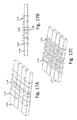
- FIG. 31 is diagram of a cuttable sheet of resonators.
- this disclosure relates to wireless energy transfer using coupled electromagnetic resonators.
- energy transfer is not restricted to electromagnetic resonators, and the wireless energy transfer systems described herein are more general and may be implemented using a wide variety of resonators and resonant objects.
- CMT coupled mode theory
- Q-factors quality factors
- impedance matching is provided, for example, in U.S. patent application Ser. No. 12/789,611 published on Sep. 23, 2010 as US 20100237709 and entitled “RESONATOR ARRAYS FOR WIRELESS ENERGY TRANSFER,” and U.S. patent application Ser. No. 12/722,050 published on Jul. 22, 2010 as US 20100181843 and entitled “WIRELESS ENERGY TRANSFER FOR REFRIGERATOR APPLICATION” and incorporated herein by reference in its entirety as if fully set forth herein.
- CMT coupled mode theory
- Q-factors quality factors
- impedance matching is provided, for example, in U.S. patent application Ser. No. 12/789,611 published on Sep. 23, 2010 as US 20100237709 and entitled “RESONATOR ARRAYS FOR WIRELESS ENERGY TRANSFER,” and U.S. patent application Ser. No. 12/722,050 published on Jul. 22, 2010 as US
- a resonator may be defined as a resonant structure that can store energy in at least two different forms, and where the stored energy oscillates between the two forms.
- the resonant structure will have a specific oscillation mode with a resonant (modal) frequency, f, and a resonant (modal) field.
- a resonator may be constructed such that the two forms of stored energy are magnetic energy and electric energy. Further, the resonator may be constructed such that the electric energy stored by the electric field is primarily confined within the structure while the magnetic energy stored by the magnetic field is primarily in the region surrounding the resonator. In other words, the total electric and magnetic energies would be equal, but their localization would be different.
- energy exchange between at least two structures may be mediated by the resonant magnetic near-field of the at least two resonators.
- These types of resonators may be referred to as magnetic resonators.
- Q Quality Factor
- the quality factor also represents the number of oscillation periods, T, it takes for the energy in the resonator to decay by a factor of e ⁇ 2 ⁇ .
- the quality factor or intrinsic quality factor or Q of the resonator is that due only to intrinsic loss mechanisms.
- the Q of a resonator connected to, or coupled to a power generator, g, or load, l, may be called the “loaded quality factor” or the “loaded Q”.
- the Q of a resonator in the presence of an extraneous object that is not intended to be part of the energy transfer system may be called the “perturbed quality factor” or the “perturbed Q”.
- Resonators coupled through any portion of their near-fields may interact and exchange energy.
- the efficiency of this energy transfer can be significantly enhanced if the resonators operate at substantially the same resonant frequency.
- a source resonator with Q s and a device resonator with Q d may utilize resonators that are high-Q.
- the of each resonator may be high.
- the geometric mean of the resonator Q's, ⁇ square root over (Q s Q d ) ⁇ may also or instead be high.
- the coupling factor, k is a number between 0 ⁇
- high-Q resonators are sub-wavelength structures.
- high-Q resonator structures are designed to have resonant frequencies higher than 100 kHz. In other embodiments, the resonant frequencies may be less than 1 GHz.
- the power radiated into the far-field by these sub wavelength resonators may be further reduced by lowering the resonant frequency of the resonators and the operating frequency of the system.
- the far field radiation may be reduced by arranging for the far fields of two or more resonators to interfere destructively in the far field.
- a resonator may be used as a wireless energy source, a wireless energy capture device, a repeater or a combination thereof.
- a resonator may alternate between transferring energy, receiving energy or relaying energy.
- one or more magnetic resonators may be coupled to an energy source and be energized to produce an oscillating magnetic near-field.
- Other resonators that are within the oscillating magnetic near-fields may capture these fields and convert the energy into electrical energy that may be used to power or charge a load thereby enabling wireless transfer of useful energy.
- the so-called “useful” energy in a useful energy exchange is the energy or power that must be delivered to a device in order to power or charge it at an acceptable rate.
- the transfer efficiency that corresponds to a useful energy exchange may be system or application-dependent. For example, high power vehicle charging applications that transfer kilowatts of power may need to be at least 80% efficient in order to supply useful amounts of power resulting in a useful energy exchange sufficient to recharge a vehicle battery without significantly heating up various components of the transfer system.
- a useful energy exchange may include any energy transfer efficiencies greater than 10%, or any other amount acceptable to keep rechargeable batteries “topped off” and running for long periods of time.
- a useful energy exchange may be any exchange that does not harm the patient but that extends the life of a battery or wakes up a sensor or monitor or stimulator. In such applications, 100 mW of power or less may be useful. In distributed sensing applications, power transfer of microwatts may be useful, and transfer efficiencies may be well below 1%.
- a useful energy exchange for wireless energy transfer in a powering or recharging application may be efficient, highly efficient, or efficient enough, as long as the wasted energy levels, heat dissipation, and associated field strengths are within tolerable limits and are balanced appropriately with related factors such as cost, weight, size, and the like.
- the resonators may be referred to as source resonators, device resonators, first resonators, second resonators, repeater resonators, and the like. Implementations may include three (3) or more resonators.
- a single source resonator may transfer energy to multiple device resonators or multiple devices. Energy may be transferred from a first device to a second, and then from the second device to the third, and so forth.
- Multiple sources may transfer energy to a single device or to multiple devices connected to a single device resonator or to multiple devices connected to multiple device resonators.
- Resonators may serve alternately or simultaneously as sources, devices, and/or they may be used to relay power from a source in one location to a device in another location.
- Intermediate electromagnetic resonators may be used to extend the distance range of wireless energy transfer systems and/or to generate areas of concentrated magnetic near-fields. Multiple resonators may be daisy-chained together, exchanging energy over extended distances and with a wide range of sources and devices. For example, a source resonator may transfer power to a device resonator via several repeater resonators. Energy from a source may be transferred to a first repeater resonator, the first repeater resonator may transfer the power to a second repeater resonator and the second to a third and so on until the final repeater resonator transfers its energy to a device resonator. In this respect the range or distance of wireless energy transfer may be extended and/or tailored by adding repeater resonators. High power levels may be split between multiple sources, transferred to multiple devices and recombined at a distant location.
- the resonators may be designed using coupled mode theory models, circuit models, electromagnetic field models, and the like.
- the resonators may be designed to have tunable characteristic sizes.
- the resonators may be designed to handle different power levels. In exemplary embodiments, high power resonators may require larger conductors and higher current or voltage rated components than lower power resonators.
- FIG. 1 shows a diagram of exemplary configurations and arrangements of a wireless energy transfer system.
- a wireless energy transfer system may include at least one source resonator (R 1 ) 104 (optionally R 6 , 112 ) coupled to an energy source 102 and optionally a sensor and control unit 108 .
- the energy source may be a source of any type of energy capable of being converted into electrical energy that may be used to drive the source resonator 104 .
- the energy source may be a battery, a solar panel, the electrical mains, a wind or water turbine, an electromagnetic resonator, a generator, and the like.
- the electrical energy used to drive the magnetic resonator is converted into oscillating magnetic fields by the resonator.
- the oscillating magnetic fields may be captured by other resonators which may be device resonators (R 2 ) 106 , (R 3 ) 116 that are optionally coupled to an energy drain 110 .
- the oscillating fields may be optionally coupled to repeater resonators (R 4 , R 5 ) that are configured to extend or tailor the wireless energy transfer region.
- Device resonators may capture the magnetic fields in the vicinity of source resonator(s), repeater resonators and other device resonators and convert them into electrical energy that may be used by an energy drain.
- the energy drain 110 may be an electrical, electronic, mechanical or chemical device and the like configured to receive electrical energy.
- Repeater resonators may capture magnetic fields in the vicinity of source, device and repeater resonator(s) and may pass the energy on to other resonators.
- a wireless energy transfer system may comprise a single source resonator 104 coupled to an energy source 102 and a single device resonator 106 coupled to an energy drain 110 .
- a wireless energy transfer system may comprise multiple source resonators coupled to one or more energy sources and may comprise multiple device resonators coupled to one or more energy drains.
- the energy may be transferred directly between a source resonator 104 and a device resonator 106 .
- the energy may be transferred from one or more source resonators 104 , 112 to one or more device resonators 106 , 116 via any number of intermediate resonators which may be device resonators, source resonators, repeater resonators, and the like.
- Energy may be transferred via a network or arrangement of resonators 114 that may include subnetworks 118 , 120 arranged in any combination of topologies such as token ring, mesh, ad hoc, and the like.
- the wireless energy transfer system may comprise a centralized sensing and control system 108 .
- parameters of the resonators, energy sources, energy drains, network topologies, operating parameters, etc. may be monitored and adjusted from a control processor to meet specific operating parameters of the system.
- a central control processor may adjust parameters of individual components of the system to optimize global energy transfer efficiency, to optimize the amount of power transferred, and the like.
- Other embodiments may be designed to have a substantially distributed sensing and control system. Sensing and control may be incorporated into each resonator or group of resonators, energy sources, energy drains, and the like and may be configured to adjust the parameters of the individual components in the group to maximize or minimize the power delivered, to maximize energy transfer efficiency in that group and the like.
- components of the wireless energy transfer system may have wireless or wired data communication links to other components such as devices, sources, repeaters, power sources, resonators, and the like and may transmit or receive data that can be used to enable the distributed or centralized sensing and control.
- a wireless communication channel may be separate from the wireless energy transfer channel, or it may be the same.
- the resonators used for power exchange may also be used to exchange information. In some cases, information may be exchanged by modulating a component in a source or device circuit and sensing that change with port parameter or other monitoring equipment.
- Resonators may signal each other by tuning, changing, varying, dithering, and the like, the resonator parameters such as the impedance of the resonators which may affect the reflected impedance of other resonators in the system.
- the systems and methods described herein may enable the simultaneous transmission of power and communication signals between resonators in wireless power transmission systems, or it may enable the transmission of power and communication signals during different time periods or at different frequencies using the same magnetic fields that are used during the wireless energy transfer.
- wireless communication may be enabled with a separate wireless communication channel such as WiFi, Bluetooth, Infrared, NFC, and the like.
- a wireless energy transfer system may include multiple resonators and overall system performance may be improved by control of various elements in the system. For example, devices with lower power requirements may tune their resonant frequency away from the resonant frequency of a high-power source that supplies power to devices with higher power requirements. For another example, devices needing less power may adjust their rectifier circuits so that they draw less power from the source. In these ways, low and high power devices may safely operate or charge from a single high power source.
- multiple devices in a charging zone may find the power available to them regulated according to any of a variety of consumption control algorithms such as First-Come-First-Serve, Best Effort, Guaranteed Power, etc.
- the power consumption algorithms may be hierarchical in nature, giving priority to certain users or types of devices, or it may support any number of users by equally sharing the power that is available in the source. Power may be shared by any of the multiplexing techniques described in this disclosure.
- electromagnetic resonators may be realized or implemented using a combination of shapes, structures, and configurations.
- Electromagnetic resonators may include an inductive element, a distributed inductance, or a combination of inductances with a total inductance, L, and a capacitive element, a distributed capacitance, or a combination of capacitances, with a total capacitance, C.
- a minimal circuit model of an electromagnetic resonator comprising capacitance, inductance and resistance, is shown in FIG. 2F .
- the resonator may include an inductive element 238 and a capacitive element 240 .
- Intrinsic losses in these electromagnetic resonators include losses due to resistance in the inductive and capacitive elements and to radiation losses, and are represented by the resistor, R, 242 in FIG. 2F .
- FIG. 2A shows a simplified drawing of an exemplary magnetic resonator structure.
- the magnetic resonator may include a loop of conductor acting as an inductive element 202 and a capacitive element 204 at the ends of the conductor loop.
- the inductor 202 and capacitor 204 of an electromagnetic resonator may be bulk circuit elements, or the inductance and capacitance may be distributed and may result from the way the conductors are formed, shaped, or positioned, in the structure.
- the inductor 202 may be realized by shaping a conductor to enclose a surface area, as shown in FIG. 2A .
- This type of resonator may be referred to as a capacitively-loaded loop inductor.
- loop or “coil” to indicate generally a conducting structure (wire, tube, strip, etc), enclosing a surface of any shape and dimension, with any number of turns.
- the enclosed surface area is circular, but the surface may be any of a wide variety of other shapes and sizes and may be designed to achieve certain system performance specifications.
- the inductance may be realized using inductor elements, distributed inductance, networks, arrays, series and parallel combinations of inductors and inductances, and the like.
- the inductance may be fixed or variable and may be used to vary impedance matching as well as resonant frequency operating conditions.
- Capacitor plates 204 may be formed and utilized as shown in FIG. 2A , or the capacitance may be distributed and be realized between adjacent windings of a multi-loop conductor.
- the capacitance may be realized using capacitor elements, distributed capacitance, networks, arrays, series and parallel combinations of capacitances, and the like.
- the capacitance may be fixed or variable and may be used to vary impedance matching as well as resonant frequency operating conditions.
- the inductive elements used in magnetic resonators may contain more than one loop and may spiral inward or outward or up or down or in some combination of directions.
- the magnetic resonators may have a variety of shapes, sizes and number of turns and they may be composed of a variety of conducing materials.
- the conductor 210 may be a wire, a Litz wire, a ribbon, a pipe, a trace formed from conducting ink, paint, gels, and the like or from single or multiple traces printed on a circuit board.
- An exemplary embodiment of a trace pattern on a substrate 208 forming inductive loops is depicted in FIG. 2B .
- the inductive elements may be formed using magnetic materials of any size, shape thickness, and the like, and of materials with a wide range of permeability and loss values. These magnetic materials may be solid blocks, they may enclose hollow volumes, they may be formed from many smaller pieces of magnetic material tiled and or stacked together, and they may be integrated with conducting sheets or enclosures made from highly conducting materials. Conductors may be wrapped around the magnetic materials to generate the magnetic field. These conductors may be wrapped around one or more than one axis of the structure. Multiple conductors may be wrapped around the magnetic materials and combined in parallel, or in series, or via a switch to form customized near-field patterns and/or to orient the dipole moment of the structure. Examples of resonators comprising magnetic material are depicted in FIGS.
- the resonator comprises loops of conductor 224 wrapped around a core of magnetic material 222 creating a structure that has a magnetic dipole moment 228 that is parallel to the axis of the loops of the conductor 224 .
- the resonator may comprise multiple loops of conductor 216 , 212 wrapped in orthogonal directions around the magnetic material 214 forming a resonator with a magnetic dipole moment 218 , 220 that may be oriented in more than one direction as depicted in FIG. 2C , depending on how the conductors are driven.
- An electromagnetic resonator may have a characteristic, natural, or resonant frequency determined by its physical properties.
- the frequency at which this energy is exchanged may be called the characteristic frequency, the natural frequency, or the resonant frequency of the resonator, and is given by ⁇ ,
- the resonant frequency of the resonator may be changed by tuning the inductance, L, and/or the capacitance, C, of the resonator.
- system parameters are dynamically adjustable or tunable to achieve as close as possible to optimal operating conditions. However, based on the discussion above, efficient enough energy exchange may be realized even if some system parameters are not variable or components are not capable of dynamic adjustment.
- a resonator may comprise an inductive element coupled to more than one capacitor arranged in a network of capacitors and circuit elements.
- the coupled network of capacitors and circuit elements may be used to define more than one resonant frequency of the resonator.
- a resonator may be resonant, or partially resonant, at more than one frequency.
- a wireless power source may comprise of at least one resonator coil coupled to a power supply, which may be a switching amplifier, such as a class-D amplifier or a class-E amplifier or a combination thereof.
- the resonator coil is effectively a power load to the power supply.
- a wireless power device may comprise of at least one resonator coil coupled to a power load, which may be a switching rectifier, such as a class-D rectifier or a class-E rectifier or a combination thereof.
- the resonator coil is effectively a power supply for the power load, and the impedance of the load directly relates also to the work-drainage rate of the load from the resonator coil.
- the efficiency of power transmission between a power supply and a power load may be impacted by how closely matched the output impedance of the power source is to the input impedance of the load.
- Power may be delivered to the load at a maximum possible efficiency, when the input impedance of the load is equal to the complex conjugate of the internal impedance of the power supply.
- Designing the power supply or power load impedance to obtain a maximum power transmission efficiency is often called “impedance matching”, and may also referred to as optimizing the ratio of useful-to-lost powers in the system.
- Impedance matching may be performed by adding networks or sets of elements such as capacitors, inductors, transformers, switches, resistors, an the like, to form impedance matching networks between a power supply and a power load.
- the impedance matching network may include variable components that are dynamically adjusted to ensure that the impedance at the power supply terminals looking towards the load and the characteristic impedance of the power supply remain substantially complex conjugates of each other, even in dynamic environments and operating scenarios.
- impedance matching may be accomplished by tuning the duty cycle, and/or the phase, and/or the frequency of the driving signal of the power supply or by tuning a physical component within the power supply, such as a capacitor.
- tuning a tuning mechanism may be advantageous because it may allow impedance matching between a power supply and a load without the use of a tunable impedance matching network, or with a simplified tunable impedance matching network, such as one that has fewer tunable components for example.
- tuning the duty cycle, and/or frequency, and/or phase of the driving signal to a power supply may yield a dynamic impedance matching system with an extended tuning range or precision, with higher power, voltage and/or current capabilities, with faster electronic control, with fewer external components, and the like.
- the parameters of the resonator such as the inductance may be affected by environmental conditions such as surrounding objects, temperature, orientation, number and position of other resonators and the like. Changes in operating parameters of the resonators may change certain system parameters, such as the efficiency of transferred power in the wireless energy transfer. For example, high-conductivity materials located near a resonator may shift the resonant frequency of a resonator and detune it from other resonant objects.
- a resonator feedback mechanism is employed that corrects its frequency by changing a reactive element (e.g., an inductive element or capacitive element). In order to achieve acceptable matching conditions, at least some of the system parameters may need to be dynamically adjustable or tunable.
- All the system parameters may be dynamically adjustable or tunable to achieve approximately the optimal operating conditions. However, efficient enough energy exchange may be realized even if all or some system parameters are not variable.
- at least some of the devices may not be dynamically adjusted.
- at least some of the sources may not be dynamically adjusted.
- at least some of the intermediate resonators may not be dynamically adjusted.
- none of the system parameters may be dynamically adjusted.
- changes in parameters of components may be mitigated by selecting components with characteristics that change in a complimentary or opposite way or direction when subjected to differences in operating environment or operating point.
- a system may be designed with components, such as capacitors, that have an opposite dependence or parameter fluctuation due to temperature, power levels, frequency, and the like.
- the component values as a function of temperature may be stored in a look-up table in a system microcontroller and the reading from a temperature sensor may be used in the system control feedback loop to adjust other parameters to compensate for the temperature induced component value changes.
- the changes in parameter values of components may be compensated with active tuning circuits comprising tunable components. Circuits that monitor the operating environment and operating point of components and system may be integrated in the design. The monitoring circuits may provide the signals necessary to actively compensate for changes in parameters of components. For example, a temperature reading may be used to calculate expected changes in, or to indicate previously measured values of, capacitance of the system allowing compensation by switching in other capacitors or tuning capacitors to maintain the desired capacitance over a range of temperatures.
- the RF amplifier switching waveforms may be adjusted to compensate for component value or load changes in the system.
- the changes in parameters of components may be compensated with active cooling, heating, active environment conditioning, and the like.
- the parameter measurement circuitry may measure or monitor certain power, voltage, and current, signals in the system, and processors or control circuits may adjust certain settings or operating parameters based on those measurements.
- the magnitude and phase of voltage and current signals, and the magnitude of the power signals, throughout the system may be accessed to measure or monitor the system performance.
- the measured signals referred to throughout this disclosure may be any combination of port parameter signals, as well as voltage signals, current signals, power signals, temperatures signals and the like. These parameters may be measured using analog or digital techniques, they may be sampled and processed, and they may be digitized or converted using a number of known analog and digital processing techniques.
- preset values of certain measured quantities are loaded in a system controller or memory location and used in various feedback and control loops, in embodiments, any combination of measured, monitored, and/or preset signals may be used in feedback circuits or systems to control the operation of the resonators and/or the system.
- Adjustment algorithms may be used to adjust the frequency, Q, and/or impedance of the magnetic resonators.
- the algorithms may take as inputs reference signals related to the degree of deviation from a desired operating point for the system and may output correction or control signals related to that deviation that control variable or tunable elements of the system to bring the system back towards the desired operating point or points.
- the reference signals for the magnetic resonators may be acquired while the resonators are exchanging power in a wireless power transmission system, or they may be switched out of the circuit during system operation. Corrections to the system may be applied or performed continuously, periodically, upon a threshold crossing, digitally, using analog methods, and the like.
- lossy extraneous materials and objects may introduce potential reductions in efficiencies by absorbing the magnetic and/or electric energy of the resonators of the wireless power transmission system. Those impacts may be mitigated in various embodiments by positioning resonators to minimize the effects of the lossy extraneous materials and objects and by placing structural field shaping elements (e.g., conductive structures, plates and sheets, magnetic material structures, plates and sheets, and combinations thereof) to minimize their effect.
- structural field shaping elements e.g., conductive structures, plates and sheets, magnetic material structures, plates and sheets, and combinations thereof
- One way to reduce the impact of lossy materials on a resonator is to use high-conductivity materials, magnetic materials, or combinations thereof to shape the resonator fields such that they avoid the lossy objects.
- a layered structure of high-conductivity material and magnetic material may tailor, shape, direct, reorient, etc. the resonator's electromagnetic fields so that they avoid lossy objects in their vicinity by deflecting the fields.
- FIG. 2D shows a top view of a resonator with a sheet of conductor 226 below the magnetic material that may used to tailor the fields of the resonator so that they avoid lossy objects that may be below the sheet of conductor 226 .
- the layer or sheet of good 226 conductor may comprise any high conductivity materials such as copper, silver, aluminum, as may be most appropriate for a given application.
- the layer or sheet of good conductor is thicker than the skin depth of the conductor at the resonator operating frequency.
- the conductor sheet may be preferably larger than the size of the resonator, extending beyond the physical extent of the resonator.
- safety measures may be included in the system.
- the packaging, structure, materials, and the like of the resonators may be designed to provide a spacing or “keep away” zone from the conducting loops in the magnetic resonator.
- high-Q resonators and power and control circuitry may be located in enclosures that confine high voltages or currents to within the enclosure, that protect the resonators and electrical components from weather, moisture, sand, dust, and other external elements, as well as from impacts, vibrations, scrapes, explosions, and other types of mechanical shock.
- enclosure may be constructed of non-lossy materials such as composites, plastics, wood, concrete, and the like and may be used to provide a minimum distance from lossy objects to the resonator components.
- a minimum separation distance from lossy objects or environments which may include metal objects, salt water, oil and the like, may improve the efficiency of wireless energy transfer.
- a “keep away” zone may be used to increase the perturbed Q of a resonator or system of resonators.
- a minimum separation distance may provide for a more reliable or more constant operating parameters of the resonators.
- resonators and their respective sensor and control circuitry may have various levels of integration with other electronic and control systems and subsystems.
- the power and control circuitry and the device resonators are completely separate modules or enclosures with minimal integration to existing systems, providing a power output and a control and diagnostics interface.
- a device is configured to house a resonator and circuit assembly in a cavity inside the enclosure, or integrated into the housing or enclosure of the device.
- FIGS. 3 and 4 show high level block diagrams depicting power generation, monitoring, and control components for exemplary sources of a wireless energy transfer system.
- FIG. 3 is a block diagram of a source comprising a half-bridge switching power amplifier and some of the associated measurement, tuning, and control circuitry.
- FIG. 4 is a block diagram of a source comprising a full-bridge switching amplifier and some of the associated measurement, tuning, and control circuitry.
- the half bridge system topology depicted in FIG. 3 may comprise a processing unit that executes a control algorithm 328 .
- the processing unit executing a control algorithm 328 may be a microcontroller, an application specific circuit, a field programmable gate array, a processor, a digital signal processor, and the like.
- the processing unit may be a single device or it may be a network of devices.
- the control algorithm may run on any portion of the processing unit.
- the algorithm may be customized for certain applications and may comprise a combination of analog and digital circuits and signals.
- the master algorithm may measure and adjust voltage signals and levels, current signals and levels, signal phases, digital count settings, and the like.
- the system may comprise an optional source/device and/or source/other resonator communication controller 332 coupled to wireless communication circuitry 312 .
- the optional source/device and/or source/other resonator communication controller 332 may be part of the same processing unit that executes the master control algorithm, it may a part or a circuit within a microcontroller 302 , it may be external to the wireless power transmission modules, it may be substantially similar to communication controllers used in wire powered or battery powered applications but adapted to include some new or different functionality to enhance or support wireless power transmission.
- the system may comprise a PWM generator 306 coupled to at least two transistor gate drivers 334 and may be controlled by the control algorithm.
- the two transistor gate drivers 334 may be coupled directly or via gate drive transformers to two power transistors 336 that drive the source resonator coil 344 through impedance matching network components 342 .
- the power transistors 336 may be coupled and powered with an adjustable DC supply 304 and the adjustable DC supply 304 may be controlled by a variable bus voltage, Vbus.
- the Vbus controller may be controlled by the control algorithm 328 and may be part of or integrated into, a microcontroller 302 or other integrated circuits.
- the Vbus controller 326 may control the voltage output of an adjustable DC supply 304 which may be used to control power output of the amplifier and power delivered to the resonator coil 344 .
- the system may comprise sensing and measurement circuitry including signal filtering and buffering circuits 318 , 320 that may shape, modify, filter, process, buffer, and the like, signals prior to their input to processors and/or converters such as analog to digital converters (ADC) 314 , 316 , for example.
- the processors and converters such as ADCs 314 , 316 may be integrated into a microcontroller 302 or may be separate circuits that may be coupled to a processing core 330 .
- the control algorithm 328 may generate, limit, initiate, extinguish, control, adjust, or modify the operation of any of the PWM generator 306 , the communication controller 332 , the Vbus control 326 , the source impedance matching controller 338 , the filter/buffering elements, 318 , 320 , the converters, 314 , 316 , the resonator coil 344 , and may be part of, or integrated into, a microcontroller 302 or a separate circuit.
- the impedance matching networks 342 and resonator coils 344 may include electrically controllable, variable, or tunable components such as capacitors, switches, inductors, and the like, as described herein, and these components may have their component values or operating points adjusted according to signals received from the source impedance matching controller 338 .
- Components may be tuned to adjust the operation and characteristics of the resonator including the power delivered to and by the resonator, the resonant frequency of the resonator, the impedance of the resonator, the Q of the resonator, and any other coupled systems, and the like.
- the resonator may be any type or structure resonator described herein including a capacitively loaded loop resonator, a planer resonator comprising a magnetic material or any combination thereof.
- the full bridge system topology depicted in FIG. 4 may comprise a processing unit that executes a master control algorithm 328 .
- the processing unit executing the control algorithm 328 may be a microcontroller, an application specific circuit, a field programmable gate array, a processor, a digital signal processor, and the like.
- the system may comprise a source/device and/or source/other resonator communication controller 332 coupled to wireless communication circuitry 312 .
- the source/device and/or source/other resonator communication controller 332 may be part of the same processing unit that executes that master control algorithm, it may a part or a circuit within a microcontroller 302 , it may be external to the wireless power transmission modules, it may be substantially similar to communication controllers used in wire powered or battery powered applications but adapted to include some new or different functionality to enhance or support wireless power transmission.
- the system may comprise a PWM generator 410 with at least two outputs coupled to at least four transistor gate drivers 334 that may be controlled by signals generated in a master control algorithm.
- the four transistor gate drivers 334 may be coupled to four power transistors 336 directly or via gate drive transformers that may drive the source resonator coil 344 through impedance matching networks 342 .
- the power transistors 336 may be coupled and powered with an adjustable DC supply 304 and the adjustable DC supply 304 may be controlled by a Vbus controller 326 which may be controlled by a master control algorithm.
- the Vbus controller 326 may control the voltage output of the adjustable DC supply 304 which may be used to control power output of the amplifier and power delivered to the resonator coil 344 .
- the system may comprise sensing and measurement circuitry including signal filtering and buffering circuits 318 , 320 and differential/single ended conversion circuitry 402 , 404 that may shape, modify, filter, process, buffer, and the like, signals prior to being input to processors and/or converters such as analog to digital converters (ADC) 314 , 316 .
- the processors and/or converters such as ADC 314 , 316 may be integrated into a microcontroller 302 or may be separate circuits that may be coupled to a processing core 330 .
- the master control algorithm may generate, limit, initiate, extinguish, control, adjust, or modify the operation of any of the PWM generator 410 , the communication controller 332 , the Vbus controller 326 , the source impedance matching controller 338 , the filter/buffering elements, 318 , 320 , differential/single ended conversion circuitry 402 , 404 , the converters, 314 , 316 , the resonator coil 344 , and may be part of or integrated into a microcontroller 302 or a separate circuit.
- Impedance matching networks 342 and resonator coils 344 may comprise electrically controllable, variable, or tunable components such as capacitors, switches, inductors, and the like, as described herein, and these components may have their component values or operating points adjusted according to signals received from the source impedance matching controller 338 .
- Components may be tuned to enable tuning of the operation and characteristics of the resonator including the power delivered to and by the resonator, the resonant frequency of the resonator, the impedance of the resonator, the Q of the resonator, and any other coupled systems, and the like.
- the resonator may be any type or structure resonator described herein including a capacitively loaded loop resonator, a planar resonator comprising a magnetic material or any combination thereof.
- Impedance matching networks may comprise fixed value components such as capacitors, inductors, and networks of components as described herein.
- Parts of the impedance matching networks, A, B and C may comprise inductors, capacitors, transformers, and series and parallel combinations of such components, as described herein.
- parts of the impedance matching networks A, B, and C may be empty (short-circuited).
- part B comprises a series combination of an inductor and a capacitor
- part C is empty.
- the full bridge topology may allow operation at higher output power levels using the same DC bus voltage as an equivalent half bridge amplifier.
- the half bridge exemplary topology of FIG. 3 may provide a single-ended drive signal, while the exemplary full bridge topology of FIG. 4 may provide a differential drive to the source resonator 308 .
- the impedance matching topologies and components and the resonator structure may be different for the two systems, as discussed herein.
- the exemplary systems depicted in FIGS. 3 and 4 may further include fault detection circuitry 340 that may be used to trigger the shutdown of the microcontroller in the source amplifier or to change or interrupt the operation of the amplifier.
- This protection circuitry may comprise a high speed comparator or comparators to monitor the amplifier return current, the amplifier bus voltage (Vbus) from the DC supply 304 , the voltage across the source resonator 308 and/or the optional tuning board, or any other voltage or current signals that may cause damage to components in the system or may yield undesirable operating conditions. Preferred embodiments may depend on the potentially undesirable operating modes associated with different applications. In some embodiments, protection circuitry may not be implemented or circuits may not be populated.
- system and component protection may be implemented as part of a master control algorithm and other system monitoring and control circuits.
- dedicated fault circuitry 340 may include an output (not shown) coupled to a master control algorithm 328 that may trigger a system shutdown, a reduction of the output power (e.g. reduction of Vbus), a change to the PWM generator, a change in the operating frequency, a change to a tuning element, or any other reasonable action that may be implemented by the control algorithm 328 to adjust the operating point mode, improve system performance, and/or provide protection.
- sources in wireless power transfer systems may use a measurement of the input impedance of the impedance matching network 342 driving source resonator coil 344 as an error or control signal for a system control loop that may be part of the master control algorithm.
- variations in any combination of three parameters may be used to tune the wireless power source to compensate for changes in environmental conditions, for changes in coupling, for changes in device power demand, for changes in module, circuit, component or subsystem performance, for an increase or decrease in the number or sources, devices, or repeaters in the system, for user initiated changes, and the like.
- changes to the amplifier duty cycle, to the component values of the variable electrical components such as variable capacitors and inductors, and to the DC bus voltage may be used to change the operating point or operating range of the wireless source and improve some system operating value.
- the specifics of the control algorithms employed for different applications may vary depending on the desired system performance and behavior.
- Impedance measurement circuitry such as described herein, and shown in FIGS. 3 and 4 , may be implemented using two-channel simultaneous sampling ADCs and these ADCs may be integrated into a microcontroller chip or may be part of a separate circuit. Simultaneously sampling of the voltage and current signals at the input to a source resonator's impedance matching network and/or the source resonator, may yield the phase and magnitude information of the current and voltage signals and may be processed using known signal processing techniques to yield complex impedance parameters. In some embodiments, monitoring only the voltage signals or only the current signals may be sufficient.
- measured voltage and current signals may be conditioned, filtered and scaled by filtering/buffering circuitry before being input to ADCs.
- the filter/buffering circuitry may be adjustable to work at a variety of signal levels and frequencies, and circuit parameters such as filter shapes and widths may be adjusted manually, electronically, automatically, in response to a control signal, by the master control algorithm, and the like. Exemplary embodiments of fitter/buffering circuits are shown in FIGS. 3 , 4 , and 5 .
- FIG. 5 shows more detailed views of exemplary circuit components that may be used in filter/buffering circuitry.
- single-ended amplifier topologies may reduce the complexity of the analog signal measurement paths used to characterize system, subsystem, module and/or component performance by eliminating the need for hardware to convert from differential to single-ended signal formats.
- differential signal formats may be preferable.
- the implementations shown in FIG. 5 are exemplary, and should not be construed to be the only possible way to implement the functionality described herein. Rather it should be understood that the analog signal path may employ components with different input requirements and hence may have different signal path architectures.
- the input current to the impedance matching networks 342 driving the resonator coils 344 may be obtained by measuring the voltage across a capacitor 324 , or via a current sensor of some type.
- the current may be sensed on the ground return path from the impedance matching network 342 .
- the input current to the impedance matching networks 342 driving the resonator coils 344 may be measured using a differential amplifier across the terminals of a capacitor 324 or via a current sensor of some type.
- the capacitor 324 may be duplicated at the negative output terminal of the source power amplifier.
- the signals may be filtered 502 to obtain the desired portions of the signal waveforms.
- the signals may be filtered to obtain the fundamental component of the signals.
- the type of filtering performed such as low pass, bandpass, notch, and the like, as well as the filter topology used, such as elliptical, Chebyshev, Butterworth, and the like, may depend on the specific requirements of the system. In some embodiments, no filtering will be required.
- the voltage and current signals may be amplified by an optional amplifier 504 .
- the gain of the optional amplifier 504 may be fixed or variable.
- the gain of the amplifier may be controlled manually, electronically, automatically, in response to a control signal, and the like.
- the gain of the amplifier may be adjusted in a feedback loop, in response to a control algorithm, by the master control algorithm, and the like.
- required performance specifications for the amplifier may depend on signal strength and desired measurement accuracy, and may be different for different application scenarios and control algorithms.
- the measured analog signals may have a DC offset added to them, 506 , which may be required to bring the signals into the input voltage range of the ADC which for some systems may be 0 to 3.3V. In some systems this stage may not be required, depending on the specifications of the particular ADC used.
- the efficiency of power transmission between a power generator and a power load may be impacted by how closely matched the output impedance of the generator is to the input impedance of the load.
- power may be delivered to the load at a maximum possible efficiency, when the input impedance of the load 604 is equal to the complex conjugate of the internal impedance of the power generator or the power amplifier 602 . Designing the generator or load impedance to obtain a high and/or maximum power transmission efficiency may be called “impedance matching”.
- Impedance matching may be performed by inserting appropriate networks or sets of elements such as capacitors, resistors, inductors, transformers, switches and the like, to form an impedance matching network 606 , between a power generator 602 and a power load 604 as shown in FIG. 6B .
- elements such as capacitors, resistors, inductors, transformers, switches and the like.
- mechanical adjustments and changes in element positioning may be used to achieve impedance matching.
- the impedance matching network 606 may include variable components that are dynamically adjusted to ensure that the impedance at the generator terminals looking towards the load and the characteristic impedance of the generator remain substantially complex conjugates of each other, even in dynamic environments and operating scenarios.
- dynamic impedance matching may be accomplished by tuning the duty cycle, and/or the phase, and/or the frequency of the driving signal of the power generator or by tuning a physical component within the power generator, such as a capacitor, as depicted in FIG. 6C .
- Such a tuning mechanism may be advantageous because it may allow impedance matching between a power generator 608 and a load without the use of a tunable impedance matching network, or with a simplified tunable impedance matching network 606 , such as one that has fewer tunable components for example.
- tuning the duty cycle, and/or frequency, and/or phase of the driving signal to a power generator may yield a dynamic impedance matching system with an extended tuning range or precision, with higher power, voltage and/or current capabilities, with faster electronic control, with fewer external components, and the like.
- the impedance matching methods, architectures, algorithms, protocols, circuits, measurements, controls, and the like, described below, may be useful in systems where power generators drive high-Q magnetic resonators and in high-Q wireless power transmission systems as described herein.
- a power generator may be a power amplifier driving a resonator, sometimes referred to as a source resonator, which may be a load to the power amplifier.
- the impedance matching may be accomplished, or accomplished in part, by tuning or adjusting the duty cycle, and/or the phase, and/or the frequency of the driving signal of the power amplifier that drives the resonator.
- Switching amplifiers such as class D, E, F amplifiers, and the like or any combinations thereof, deliver power to a load at a maximum efficiency when almost no power is dissipated on the switching elements of the amplifier.
- This operating condition may be accomplished by designing the system so that the switching operations which are most critical (namely those that are most likely to lead to switching losses) are done when either or both of the voltage across the switching element and the current through the switching element are nearly zero. These conditions may be referred to as Zero Voltage Switching (ZVS) and Zero Current Switching (ZCS) conditions respectively.
- ZVS Zero Voltage Switching
- ZCS Zero Current Switching
- a switching amplifier may convert DC (or very low frequency AC) power to AC power at a specific frequency or range of frequencies, a filter may be introduced before the load to prevent unwanted harmonics that may be generated by the switching process from reaching the load and being dissipated there.
- the value of the characteristic impedance of the amplifier may depend on the operating frequency, the amplifier topology, and the switching sequence of the switching elements.
- the switching amplifier may be a half-bridge topology and, in some embodiments, a full-bridge topology.
- the switching amplifier may be class D and, in some embodiments, class E.
- ⁇ is the frequency at which the switching elements are switched
- the driven load may have impedance that is very different from the characteristic impedance of the external driving circuit, to which it is connected. Furthermore, the driven load may not be a resonant network.
- An Impedance Matching Network is a circuit network that may be connected before a load as in FIG. 6B , in order to regulate the impedance that is seen at the input of the network consisting of the IMN circuit and the load. An IMN circuit may typically achieve this regulation by creating a resonance close to the driving frequency.
- an IMN circuit may be used between the driving circuit and the load.
- impedance matching between the load and the external driving circuit may be achieved by using adjustable/tunable components in the IMN circuit that may be adjusted to match the varying load to the fixed characteristic impedance Z O of the external circuit ( FIG. 6B ). To match both the real and imaginary parts of the impedance two tunable/variable elements in the IMN circuit may be needed.
- the load may be inductive (such as a resonator coil) with impedance R+j ⁇ L, so the two tunable elements in the IMN circuit may be two tunable capacitance networks or one tunable capacitance network and one tunable inductance network or one tunable capacitance network and one tunable mutual inductance network.
- the impedance matching between the load and the driving circuit may be achieved by using adjustable/tunable components or parameters in the amplifier circuit that may be adjusted to match the characteristic impedance Z O of the amplifier to the varying (due to load variations) input impedance of the network consisting of the IMN circuit and the load (IMN+load), where the IMN circuit may also be tunable ( FIG. 6C ).
- adjustable/tunable components or parameters in the amplifier circuit may be adjusted to match the characteristic impedance Z O of the amplifier to the varying (due to load variations) input impedance of the network consisting of the IMN circuit and the load (IMN+load), where the IMN circuit may also be tunable ( FIG. 6C ).
- a total of two tunable/variable elements or parameters in the amplifier and the IMN circuit may be needed.
- the disclosed impedance matching method can reduce the required number of tunable/variable elements in the IMN circuit or even completely eliminate the requirement for tunable/variable elements in the IMN circuit.
- one tunable element in the power amplifier and one tunable element in the IMN circuit may be used.
- two tunable elements in the power amplifier and no tunable element in the IMN circuit may be used.
- the tunable elements or parameters in the power amplifier may be the frequency, amplitude, phase, waveform, duty cycle and the like of the drive signals applied to transistors, switches, diodes and the like.
- the power amplifier with tunable characteristic impedance may be a tunable switching amplifier of class D, E, F or any combinations thereof.
- one tunable element may be the capacitance C ⁇ , which may be tuned by tuning the external capacitors placed in parallel with the switching elements.
- one tunable element may be the duty cycle dc of the ON switch-state of the switching elements of the amplifier. Adjusting the duty cycle, dc, via Pulse Width Modulation (PWM) has been used in switching amplifiers to achieve output power control.
- PWM Pulse Width Modulation
- PWM may also be used to achieve impedance matching, namely to satisfy Eqs. (3), and thus maximize the amplifier efficiency.
- one tunable element may be the switching frequency, which is also the driving frequency of the IMN+load network and may be designed to be substantially close to the resonant frequency of the IMN+load network. Tuning the switching frequency may change the characteristic impedance of the amplifier and the impedance of the IMN+load network. The switching frequency of the amplifier may be tuned appropriately together with one more tunable parameters, so that Eqs. (3) are satisfied.
- a benefit of tuning the duty cycle and/or the driving frequency of the amplifier for dynamic impedance matching is that these parameters can be tuned electronically, quickly, and over a broad range.
- a tunable capacitor that can sustain a large voltage and has a large enough tunable range and quality factor may be expensive, slow or unavailable for with the necessary component specifications
- FIG. 8 A simplified circuit diagram showing the circuit level structure of a class D power amplifier 802 , impedance matching network 804 and an inductive load 806 is shown in FIG. 8 .
- the diagram shows the basic components of the system with the switching amplifier 804 comprising a power source 810 , switching elements 808 , and capacitors.
- the impedance matching network 804 comprising inductors and capacitors, and the load 806 modeled as an inductor and a resistor.
- An exemplary embodiment of this inventive tuning scheme comprises a half-bridge class-D amplifier operating at switching frequency f and driving a low-loss inductive element R+j ⁇ L via an IMN, as shown in FIG. 8 .
- L′ may be tunable.
- L′ may be tuned by a variable tapping point on the inductor or by connecting a tunable capacitor in series or in parallel to the inductor.
- C ⁇ may be tunable.
- C ⁇ may be tuned by varying either one or both capacitors C switc , as only the parallel sum of these capacitors matters for the amplifier operation.
- C ⁇ may be tuned by varying either one, two, three or all capacitors C switc , as only their combination (series sum of the two parallel sums associated with the two halves of the bridge) matters for the amplifier operation.
- two of the components of the IMN may be tunable.
- L′ and C 2 may be tuned.
- elements in the switching amplifier may also be tunable.
- the capacitance C ⁇ along with the IMN capacitor C 2 may be tuned.
- the duty cycle dc along with the IMN capacitor C 2 may be tuned.
- the capacitance C ⁇ along with the IMN inductor L′ may be tuned.
- the duty cycle dc along with the IMN inductor L′ may be tuned.
- dynamic impedance matching with fixed elements inside the IMN may be achieved by varying the driving frequency of the external frequency f (e.g. the switching frequency of a switching amplifier) so that it follows the varying resonant frequency of the resonator.
- the driving frequency of the external frequency f e.g. the switching frequency of a switching amplifier
- full impedance matching can be achieved as R and L are varying without the need of any variable components.
- the low-loss inductive element may be the coil of a source resonator coupled to one or more device resonators or other resonators, such as repeater resonators, for example.
- the impedance of the inductive element R+j ⁇ L may include the reflected impedances of the other resonators on the coil of the source resonator.
- Variations of R and L of the inductive element may occur due to external perturbations in the vicinity of the source resonator and/or the other resonators or thermal drift of components. Variations of R and L of the inductive element may also occur during normal use of the wireless power transmission system due to relative motion of the devices and other resonators with respect to the source.
- dynamic impedance matching may be achieved at the source circuit. In some embodiments, dynamic impedance matching may also be achieved at the device circuit.
- the effective resistance of the source inductive element namely the resistance of the source coil R s plus the reflected impedance from the device
- the resistance R represents both the source coil and the reflected impedances of the device coils to the source coil
- the required output power of the source circuit may need to decrease as U increases. If dynamic impedance matching is achieved via tuning some of the amplifier parameters, the output power of the amplifier may vary accordingly.
- the automatic variation of the output power is preferred to be monotonically decreasing with R, so that it matches the constant device power requirement.
- the output power level is accomplished by adjusting the DC driving voltage of the power generator, using an impedance matching set of tunable parameters which leads to monotonically decreasing output power vs. R will imply that constant power can be kept at the power load in the device with only a moderate adjustment of the DC driving voltage.
- the “knob” to adjust the output power level is the duly cycle de or the phase of a switching amplifier or a component inside an Impedance Matching Network, using an impedance matching set of tunable parameters which leads to monotonically decreasing output power vs. R will imply that constant power can be kept at the power load in the device with only a moderate adjustment of this power “knob”.
- dynamic impedance matching may be achieved at the source circuit, but impedance matching may not be achieved or may only partially be achieved at the device circuit.
- the varying reflected impedance of the device to the source may result in a variation of both the effective resistance R and the effective inductance L of the source inductive element.
- Tuning the duty cycle dc of the switching amplifier and the capacitor C 2s may be used to dynamically impedance match the source, as the non-tunable device is moving relatively to the source changing the mutual inductance M between the source and the device.
- FIG. 14 we show the required values of the tunable parameters along with the output power per DC voltage of the amplifier. The dashed line again indicates the output power of the amplifier that would be needed so that the power at the load is a constant value.
- tuning the driving frequency f of the source driving circuit may still be used to achieve dynamic impedance matching at the source for a system of wireless power transmission between the source and one or more devices.
- this method enables full dynamic impedance matching of the source, even when there are variations in the source inductance L s and thus the source resonant frequency.
- the device resonant frequencies must be tuned to follow the variations of the matched driving and source-resonant frequencies. Tuning a device capacitance (for example, in the embodiment of FIG. 13 C 1d or C 2d ) may be necessary, when there are variations in the resonant frequency of either the source or the device resonators.
- tuning the driving frequency alleviates the need to tune only one source-object resonant frequency, however, all the rest of the objects may need a mechanism (such as a tunable capacitance) to tune their resonant frequencies to match the driving frequency.
- Energy may be dissipated in the resonator components themselves. For example, even high-Q conductors and components have some loss or resistance, and these conductors and components may heat up when electric currents and/or electromagnetic fields flow through them. Energy may be dissipated in materials and objects around a resonator. For example, eddy currents dissipated in imperfect conductors or dielectrics surrounding or near-by the resonator may heat up those objects. In addition to affecting the material properties of those objects, this heat may be transferred through conductive, radiative, or convective processes to the resonator components. Any of these heating effects may affect the resonator Q, impedance, frequency, etc., and therefore the performance of the wireless energy transfer system.
- heat may be generated in the magnetic material due to hysteresis losses and to resistive losses resulting from induced eddy currents. Both effects depend on the magnetic flux density in the material, and both can create significant amounts of heat, especially in regions where the flux density or eddy currents may be concentrated or localized. In addition to the flux density, the frequency of the oscillating magnetic field, the magnetic material composition and losses, and the ambient or operating temperature of the magnetic material may all impact how hysteresis and resistive losses heat the material.
- the properties of the magnetic material such as the type of material, the dimensions of the block, and the like, and the magnetic field parameters may be chosen for specific operating power levels and environments to minimize heating of the magnetic material.
- changes, cracks, or imperfections in a block of magnetic material may increase the losses and heating of the magnetic material in wireless power transmission applications.
- the losses in the block may be uneven and may be concentrated in regions where there are inhomogeneities or relatively narrow gaps between adjacent tiles or pieces of magnetic material.
- the effective reluctance of various magnetic flux paths through the material may be substantially irregular and the magnetic field may be more concentrated in portions of the block where the magnetic reluctance is lowest.
- the effective reluctance may be lowest where the gap between tiles or pieces is narrowest or where the density of imperfections is lowest.
- the magnetic flux density may not be substantially uniform across the block, but may be concentrated in regions offering relatively lower reluctance. Irregular concentrations of the magnetic field within a block of magnetic material may not be desirable because they may result in uneven losses and heat dissipation in the material.
- a magnetic resonator comprising a conductor 1506 wrapped around a block of magnetic material composed of two individual tiles 1502 , 1504 of magnetic material joined such that they form a seam 1508 that is perpendicular to the axis of the conductor 1506 loops as depicted in FIG. 15 .
- An irregular gap in the seam 1508 between the tiles of magnetic material 1502 , 1504 may force the magnetic field 1512 (represented schematically by the dashed magnetic field lines) in the resonator to concentrate in a sub region 1510 of the cross section of the magnetic material.
- a path including an air gap between two pieces of magnetic material may create an effectively higher reluctance path than one that traverses the width of the magnetic material at a point where the pieces of magnetic materials touch or have a smaller air gap.
- the magnetic flux density may therefore preferentially flow through a relatively small cross area of the magnetic material resulting in a high concentration of magnetic flux in that small area 1510 .
- the more inhomogeneous flux density distributions lead to higher overall losses.
- the more inhomogeneous flux distribution may result in material saturation and cause localized heating of the area in which the magnetic flux is concentrated.
- the localized heating may alter the properties of the magnetic material, in some cases exacerbating the losses.
- hysteresis and resistive losses increase with temperature. If heating the material increases material losses, resulting in more heating, the temperature of the material may continue to increase and even runaway if no corrective action is taken. In some instances, the temperature may reach 100 C or more and may degrade the properties of the magnetic material and the performance of wireless power transfer.
- the magnetic materials may be damaged, or the surrounding electronic components, packaging and/or enclosures may be damaged by the excessive heat.
- variations or irregularities between tiles or pieces of the block of magnetic material may be minimized by machining, polishing, grinding, and the like, the edges of the tiles or pieces to ensure a tight fit between tiles of magnetic materials providing a substantially more uniform reluctance through the whole cross section of the block of magnetic material.
- a block of magnetic material may require a means for providing a compression force between the tiles to ensure the tiles are pressed tight together without gaps.
- an adhesive may be used between the tiles to ensure they remain in tight contact.
- the irregular spacing of adjacent tiles of magnetic material may be reduced by adding a deliberate gap between adjacent tiles of magnetic material.
- a deliberate gap may be used as a spacer to ensure even or regular separations between magnetic material tiles or pieces. Deliberate gaps of flexible materials may also reduce irregularities in the spacings due to tile movement or vibrations.
- the edges of adjacent tiles of magnetic material may be taped, dipped, coated, and the like with an electrical insulator, to prevent eddy currents from flowing through reduced cross-sectional areas of the block, thus lowering the eddy current losses in the material.
- a separator may be integrated into the resonator packaging. The spacer may provide a spacing of 1 mm or less.
- the mechanical properties of the spacer between tiles may be chosen so as to improve the tolerance of the overall structure to mechanical effects such as changes in the dimensions and/or shape of the tiles due to intrinsic effects (e.g, magnetostriction, thermal expansion, and the like) as well as external shocks and vibrations.
- the spacer may have a desired amount of mechanical give to accommodate the expansion and/or contraction of individual tiles, and may help reduce the stress on the tiles when they are subjected to mechanical vibrations, thus helping to reduce the appearance of cracks and other defects in the magnetic material.
- the individual tiles that comprise the block of magnetic material may be preferable to arrange the individual tiles that comprise the block of magnetic material to minimize the number of seams or gaps between tiles that are perpendicular to the dipole moment of the resonator. In embodiments it may be preferable to arrange and orient the tiles of magnetic material to minimize the gaps between tiles that are perpendicular to the axis formed by the loops of a conductor comprising the resonator.
- the resonator comprises a conductor 1604 wrapped around a block of magnetic material comprising six separate individual tiles 1602 arranged in a three by two array.
- the arrangement of tiles results in two tile seams 1606 , 1608 when traversing the block of magnetic material in one direction, and only one tile seam 1610 when traversing the block of magnetic material in the orthogonal direction.
- seams and gaps 1606 , 1608 that are parallel to the dipole moment of the resonator.
- Seams and gaps that run perpendicular to the dipole moment of the resonator may also be referred to as critical seams or critical seam areas. It may still be desirable, however, to electrically insulate gaps that run parallel to the dipole moment of the resonator (such as 1606 and 1608 ) so as to reduce eddy current losses. Uneven contact between tiles separated by such parallel gaps may cause eddy currents to flow through narrow contact points, leading to large losses at such points.
- irregularities in spacing may be tolerated with adequate cooling of the critical seam areas to prevent the localized degradation of material properties when the magnetic material heats up. Maintaining the temperature of the magnetic material below a critical temperature may prevent a runaway effect caused by a sufficiently high temperature. With proper cooling of the critical seam area, the wireless energy transfer performance may be satisfactory despite the additional loss and heating effects due to irregular spacing, cracks, or gaps between tiles.
- Effective heatsinking of the resonator structure to prevent excessive localized heating of the magnetic material poses several challenges.
- Metallic materials that are typically used for heatsinks and thermal conduction can interact with the magnetic fields used for wireless energy transfer by the resonators and affect the performance of the system. Their location, size, orientation, and use should be designed so as to not excessively lower the perturbed Q of the resonators in the presence of these heatsinking materials.
- a relatively large contact area between the heatsink and the magnetic material may be required to provide adequate cooling which may require placement of substantial amount of lossy materials close to the magnetic resonator.
- adequate cooling of the resonator may be achieved with minimal effect on the wireless energy transfer performance with strategic placement of thermally conductive materials.
- strips of thermally conductive material may be placed in between loops of conductor wire and in thermal contact with the block of magnetic material.
- FIG. 17 One exemplary embodiment of a resonator with strips of thermally conductive material is depicted in FIG. 17 .
- FIG. 17A shows the resonator structure without the conducting strips and with the block of magnetic material comprising smaller tiles of magnetic material forming gaps or seams.
- Strips of thermally conductive 1708 material may be placed in between the loops of the conductor 1702 and in thermal contact with the block of magnetic material 1704 as depicted in FIGS. 17B and 17C .
- the strips of conductor may be placed to cover as much or as many of the seams or gaps between the tiles as possible especially the seams between tiles that are perpendicular to the dipole moment of the resonator.
- the thermally conductive material may comprise copper, aluminum, brass, thermal epoxy, paste, pads, and the like, and may be any material that has a thermal conductivity that is at least that of the magnetic material in the resonator ( ⁇ 5 W/(K-m) for some commercial ferrite materials).
- the thermally conductive material is also electrically conducting, the material may require a layer or coating of an electrical insulator to prevent shorting and direct electrical contact with the magnetic material or the loops of conductor of the resonator.
- the strips of thermally conductive material may be used to conduct heat from the resonator structure to a structure or medium that can safely dissipate the thermal energy.
- the thermally conductive strips may be connected to a heat sink such as a large plate located above the strips of conductor that can dissipate the thermal energy using passive or forced convection, radiation, or conduction to the environment.
- the system may include any number of active cooling systems that may be external or internal to the resonator structure that can dissipate the thermal energy from the thermally conducting strips and may include liquid cooling systems, forced air systems, and the like.
- the thermally conducting strips may be hollow or comprise channels for coolant that may be pumped or forced through to cool the magnetic material.
- a field deflector made of a good electrical conductor may double as part of the heatsinking apparatus.
- the addition of thermally and electrically conducting strips to the space between the magnetic material and the field deflector may have a marginal effect on the perturbed Q, as the electromagnetic fields in that space are typically suppressed by the presence of the field deflector.
- Such conducting strips may be thermally connected to both the magnetic material and the field deflector to make the temperature distribution among different strips more homogeneous.
- the thermally conducting strips are spaced to allow at least one loop of conductor to wrap around the magnetic material.
- the strips of thermally conductive material may be positioned only at the gaps or seams of the magnetic material.
- the strips may be positioned to contact the magnetic material at substantially throughout its complete length.
- the strips may be distributed to match the flux density within the magnetic material. Areas of the magnetic material which under normal operation of the resonator may have higher magnetic flux densities may have a higher density of contact with the thermally conductive strips.
- the highest magnetic flux density in the magnetic material may be observed toward the center of the block of magnetic material and the lower density may be toward the ends of the block in the direction of the dipole moment of the resonator.
- the inventors have performed a finite element simulation of a resonator structure similar to that depicted in FIG. 17C .
- the structure was simulated operating at a frequency of 235 kHz and comprising a block of EPCOS N95 magnetic material measuring 30 cm ⁇ 30 cm ⁇ 5 mm excited by 10 turns of litz wire (symmetrically placed at 25 mm, 40 mm, 55 mm, 90 mm and 105 mm from the plane of symmetry of the structure) carrying 40 A of peak current each, and thermally connected to a 50 cm ⁇ 50 cm ⁇ 4 mm field deflector by means of three 3 ⁇ 3 ⁇ 4 ⁇ 1′ hollow square tubes (1 ⁇ 8′′ wall thickness) of aluminum (alloy 6063) whose central axes are placed at ⁇ 75 mm, 0 mm, and +75 from the symmetry plane of the structure.
- the perturbed Q due to the field deflector and hollow tubes was found to be 1400 (compared to 1710 for the same structure without the hollow tubes).
- the power dissipated in the shield and tubes was calculated to be 35.6 W, while that dissipated in the magnetic material was 58.3 W.
- the maximum temperature in the structure was 85° C. (at points in the magnetic material approximately halfway between the hollow tubes) while the temperature in parts of the magnetic material in contact with the hollow tubes was approximately 68° C.
- the same resonator without the thermally conducting hollow tubes dissipated 62.0 W in the magnetic material for the same excitation current of 40 W peak and the maximum temperature in the magnetic material was found to be 111° C.
- thermally conductive strips of material may be positioned at areas that may have the highest probability of developing cracks that may cause irregular gaps in the magnetic material. Such areas may be areas of high stress or strain on the material, or areas with poor support or backing from the packaging of the resonator. Strategically positioned thermally conductive strips may ensure that as cracks or irregular gaps develop in the magnetic material, the temperature of the magnetic material will be maintained below its critical temperature.
- the critical temperature may be defined as the Curie temperature of the magnetic material, or any temperature at which the characteristics of the resonator have been degraded beyond the desired performance parameters.
- the heastsinking structure may provide mechanical support to the magnetic material.
- the heatsinking structure may be designed to have a desired amount of mechanical give (e.g., by using epoxy, thermal pads, and the like having suitable mechanical properties to thermally connect different elements of the structure) so as to provide the resonator with a greater amount of tolerance to changes in the intrinsic dimensions of its elements (due to thermal expansion, magnetostriction, and the like) as well as external shocks and vibrations, and prevent the formation of cracks and other defects.
- the strips of conducting material may be tailored to make thermal contact with the magnetic material within areas delimited by two orthogonal sets of adjacent loops.
- a strip may contain appropriate indentations to fit around the conductor of at least one orthogonal winding while making thermal contact with the magnetic material at least one point.
- the magnetic material may be in thermal contact with a number of thermally conducting blocks placed between adjacent loops. The thermally conducting blocks may be in turn thermally connected to one another by means of a good thermal conductor and/or heatsinked.
- thermally conductive strips of material was used as an exemplary specimen of a shape of a material it should be understood by those skilled in the art that any shapes and contours may be substituted without departing from the spirit of the inventions. Squared, ovals, strips, dots, elongated shapes, and the like would all be within the spirit of the present invention.
- a wireless energy transfer system may require a verification step to ensure that energy is being transferred between designated resonators.
- source resonators, device resonators, and repeater resonators do not require physical contact with each other in order to exchange energy, and these resonators may be separated from each other by distances of centimeters or meters, depending on the size and number of resonators in the system.
- multiple resonators may be in a position to generate or receive power, but only two or some of those resonators are designated resonators.
- Communication of information between resonators in a wireless energy transfer system may be utilized to designate resonators. Communication of information between resonators may be implemented using in-band or out-of-band communications or communications channels. If at least some part of a magnetic resonator used to exchange power is also used to exchange information, and the carrier frequency of the information exchange is close to the resonant frequency used in the power exchange, we refer to that communication as in-band. Any other type of communication between magnetic resonators is referred to as out-of-band.
- An out-of-band communication channel may use an antenna and a signaling protocol that is separated from the energy transfer resonator and magnetic fields.
- An out-of-band communication channel may use or be based on Bluetooth, WiFi, Zigbee, NFC technology and the like.
- Communication between resonators may be used to coordinate the wireless energy transfer or to adjust the parameters of a wireless energy transfer system, to identify and authenticate available power sources and devices, to optimize efficiency, power delivery, and the like, to track and bill energy preferences, usage, and the like, and to monitor system performance, battery condition, vehicle health, extraneous objects, also referred to as foreign objects, and the like.
- Methods for designating and verifying resonators for energy transfer may be different when in-band and out-of-band communication channels are used because the distance over which communication signals may be exchanged using out-of-band techniques may greatly exceed the distance over which the power signals may be exchanged. Also, the bandwidth of out-of-band communication signals may be larger than in-band communication signals.
- This difference in communication range and capability may affect the coordination of the wireless energy transfer system.
- the number of resonators that may be addressed using out-of-band communication may be very large and communicating resonators may be farther apart than the distance over which they may efficiently exchange energy.
- all of the signaling and communication may be performed using an in-band communication channel and the signals may be modulated on the fields used for energy transfer.
- in-band communication may use substantially the same frequency spectrum as is used for energy transfer, but communication may occur while useful amounts of energy are not being transmitted.
- Using only the in-band communication channel may be preferable if separate or multiple verification steps are problematic, because the range of the communication may be limited to the same range as the power exchange or because the information arrives as a modulation on the power signal itself.
- a separate out-of-band communication channel may be more desirable.
- an out-of-band communication channel may be less expensive to implement and may support higher data rates.
- An out-of-band communication channel may support longer distance communication, allowing resonator discovery and power system mapping.
- An out-of-band communication channel may operate regardless of whether or not power transfer is taking place and may occur without disruption of the power transfer.
- FIG. 18 An exemplary embodiment of a wireless energy system is shown in FIG. 18 .
- This exemplary embodiment comprises two device resonators 1802 , 1816 each with an out-of-band communication module 1804 , 1818 respectively and two source resonators 1806 , 1810 each with their own out-of-band communication modules 1808 , 1812 respectively.
- the system may use the out-of-band communication channel to adjust and coordinate the energy transfer.
- the communication channel may be used to discover or find resonators in the proximity, to initiate power transfer, and to communicate adjustment of operating parameters such as power output, impedance, frequency, and the like of the individual resonators.
- a device resonator may incorrectly communicate with one source but receive energy from another source resonator.
- device 1802 sends an out-of-band communication signal requesting power from a source.
- Source 1810 may respond and begin to supply power to device 1802 .
- device 1816 also sends an out-of-band communication signal requesting power from a source and that source 1806 responds and begins to supply power to device 1816 .
- device 1802 Because of the proximity of device 1802 to source 1806 , it is possible that device 1802 receives some or most of its power from source 1806 . If the power level received by device 1802 becomes too high, device 1802 may send an out-of-band communication signal to source 1810 to reduce the power it is transmitting to device 1802 . However, device 1802 may still be receiving too much power, because it is receiving power from source 1806 but is not communicating control signals to that source 1806 .
- the separation of the energy transfer channel and the communication channel may create performance, control, safety, security, reliability, and the like issues in wireless energy transfer systems.
- it may be necessary for resonators in a wireless energy transfer system to identify/designate and verify any and all resonators with which it is exchanging power.
- the example shown in FIG. 18 is just one example and there exist many configurations and arrangements of wireless power transmission systems that may benefit from explicit or implicit energy transfer verification steps.
- the potential performance, control, safety, security, reliability and the like, issues may be avoided by providing at least one verification step that insures that the energy transfer channel and the communication channel used by a pair of resonators are associated with the same pair of resonators.
- the verification step may comprise some additional information exchange or signaling through the wireless energy transfer channel.
- a verification step comprising communication or information exchange using the energy transfer channel, or fields of the energy transfer channel may be used to verify that the out-of-band communication channel is exchanging information between the same two resonators that are or will be exchanging energy.
- the verification step may be implicit or explicit.
- verification may be implicit.
- an energy transfer channel may be implicitly verified by monitoring and comparing the behavior of the energy transfer channel to expected behavior or parameters in response to the out-of-band information exchange. For example, after establishing out-of-band communications, a device may request that a wireless source increase the amount of power it is transmitting. At the same time, parameters of the wireless energy transfer channel and resonators may be monitored. An observed increase of delivered power at the device may be used to infer that the out-of-band communication channel and the energy transfer channel are correctly linked to the designated resonators.
- an implicit verification step may involve monitoring any number of the parameters of the wireless energy transfer or parameters of the resonators and components used in the wireless energy transfer.
- the currents, voltages, impedances, frequency, efficiency, temperatures, of the resonators and their drive circuits and the like may be monitored and compared to expected values, trends, changes and the like as a result of an out-of-band communication exchange.
- a resonator may store tables of measured parameters and expected values, trends, and/or changes to these parameters as a consequence of a communication exchange.
- a resonator may store a history of communications and observed parameter changes that may be used to verify the energy transfer channel. In some cases a single unexpected parameter change due to a communication exchange may be not be conclusive enough to determine the out-of-band channel is incorrectly paired. In some embodiments the history of parameter changes may be scanned or monitored over several or many communication exchanges to perform verification.
- FIG. 19A An example algorithm showing the series of steps which may be used to implicitly verify an energy transfer channel in a wireless energy transfer system using out-of-band communication is shown in FIG. 19A .
- an out-of-band communication channel between a source and a device is established.
- the source and device may exchange information regarding adjusting the parameters of the wireless energy transfer or parameters of the components used for wireless energy transfer.
- the information exchange on the out-of-band communication channel may be a normal exchange used in normal operation of the system to control and adjust the energy transfer.
- the out-of-band communication channel may be encrypted preventing eavesdropping, impersonation, and the like.
- the source and the device or just a source or just a device may monitor and keep track of any changes to the parameters of the wireless energy transfer or any changes in parameters in the components used in the energy transfer.
- the tracked changes may be compared against expected changes to the parameters as a consequence of any out-of-band communication exchanges. Validation may be considered failed when one or many observed changes in parameters do not correspond to expected changes in parameters.
- verification may be explicit.
- a source or a device may alter, dither, modulate, and the like the parameters of the wireless energy transfer or the parameters of the resonators used in the wireless energy transfer to communicate or provide a verifiable signal to a source or device through the energy transfer channel.
- the explicit verification may involve changing, altering, modulating, and the like some parameters of the wireless energy transfer or the parameters of the resonators and components used in the energy transfer for the explicit purpose of verification and may not be associated with optimizing, tuning, or adjusting the energy transfer.
- the changing, altering, modulating, and the like some parameters of the wireless energy transfer or the parameters of the resonators and components used in the energy transfer for the purpose of signaling or communicating with another wireless energy resonator or component may also be referred to as in-band communication.
- the in-band communication channel may be implemented as part of the wireless energy transfer resonators and components.
- Information may be transmitted from one resonator to another by changing the parameters of the resonators. Parameters such as inductance, impedance, resistance, and the like may be dithered or changed by one resonator. These changes may affect the impedance, resistance, or inductance of other resonators around the signaling resonator.
- in-band communication may comprise altering, changing, modulating, and the like the power level, amplitude, phase, orientation, frequency, and the like of the magnetic fields used for energy transfer.
- the explicit in-band verification may be performed after an out-of-band communication channel has been established.
- a source and a device may exchange information as to the power transfer capabilities and in-band signaling capabilities.
- Wireless energy transfer between a source and a device may then be initiated.
- the source or device may request or challenge the other source or device to signal using the in-band communication channel to verify the connection between the out-of-band and communication channel and the energy transfer channel.
- the channel is verified when the agreed signaling established in the out-of-band communication channel is observed at the in-band communication channel.
- verification may be performed only during specific or pre-determined times of an energy exchange protocol such as during energy transfer startup.
- explicit verification steps may be performed periodically during the normal operation of the wireless energy transfer system. The verification steps may be triggered when the efficiency or characteristics of the wireless power transfer change which may signal that the physical orientations have changed.
- the communication controller may maintain a history of the energy transfer characteristics and initiate a verification of the transfer that includes signaling using the resonators when a change in the characteristics is observed. A change in the energy transfer characteristics may be observed as a change in the efficiency of the energy transfer, the impedance, voltage, current, and the like of the resonators, or components of the resonators and power and control circuitry.
- a signaling and communication channel capable of transmitting messages may be secured with any number of encryption, authentication, and security algorithms.
- the out-of-band communication may be encrypted and the secured communication channel may be used to transmit random sequences for verification using the in-band channel.
- the in-band communication channel may be encrypted, randomized, or secured by any known security and cryptography protocols and algorithms.
- the security and cryptography algorithms may be used to authenticate and verify compatibility between resonators and may use a public key infrastructure (PKI) and secondary communication channels for authorization and authentication.
- PKI public key infrastructure
- a device may verify the energy transfer channel to ensure it is receiving energy from the desired or assumed source.
- a source may verify the energy transfer channel to ensure energy is being transferred to the desired or assumed source.
- the verification may be bidirectional and a source and device may both verify their energy transfer channels in one step or protocol operation.
- there may be more than two resonators and there may be repeater resonators.
- communication and control may be centralized in one or a few resonators or communication and control may be distributed across many, most, or all the resonators in a network.
- communication and/or control may be effected by one or more semiconductor chips or microcontrollers that are coupled to other wireless energy transfer components.
- FIG. 19B An example algorithm showing the series of steps which may be used to explicitly verify an energy transfer channel in a wireless energy transfer system using out-of-band communication is shown in FIG. 19B .
- the first step 1908 an out-of-band communication channel between a source and a device is established.
- the source and device may coordinate or agree on a signaling protocol, method, scheme, and the like that may be transmitted through the wireless energy transfer channel.
- the out-of-band communication channel may be encrypted and the source and device may follow any number of known cryptographic authentication protocols.
- the verification code may comprise a challenge-response type exchange which may provide an additional level of security and authentication capability.
- a device may challenge the source to encrypt a random verification code which it sends to the source via the out-of-band communication channel using a shared secret encryption key or a private key.
- the verification code transmitted in the out-of-band communication channel may then be signaled 1912 through the in-band communication channel.
- the verification code signaled in the in-band communication channel may be encrypted or modified by the sender with a reversible cryptographic function allowing the receiver to further authenticate the sender and verify that the in-band communication channels are linked with the same source or device associated with the out-of-band communication channel.
- a wireless energy transfer system may try to repeat the validation procedure.
- the system may try to re-validate the wireless energy transfer channel by exchanging another verification sequence for resignaling using the in-band communication channel.
- the system may change or alter the sequence or type of information that is used to verify the in-band communication channel after attempts to verify the in-band communication channel have failed.
- the system may change the type of signaling, protocol, length, complexity and the like of the in-band communication verification code.
- the system may adjust the power level, the strength of modulation, frequency of modulation and the like of the signaling method in the in-band communication channel. For example, upon failure of verification of a source by a device, the system may attempt to perform the verification at a higher energy transfer level. The system may increase the power output of the source generating stronger magnetic fields. In another example, upon failure of verification of a source by a device, the source that communicated the verification code to the device by changing the impedance of its source resonator may increase or even double the amount of change in the impedance of the source resonator for the signaling.
- the system may try to probe, find, or discover other possible sources or devices using the out-of-band communication channel.
- the out-of-band communication channel may be used to find other possible candidates for wireless energy transfer.
- the system may change or adjust the output power or the range of the out-of-band communication channel to help minimize false pairings.
- the out-of-band communication channel may be power modulated to have several modes, long range mode to detect sources and a short range or low power mode to ensure the communication is with another device or source that is within a specified distance.
- the out-of-band communication channel may be matched to the range of the wireless channel for each application. After failure of verification of the energy transfer channel the output power of the out-of-band communication channel may be slowly increased to find other possible sources or devices for wireless energy transfer.
- an out-of-band communication channel may exhibit interferences and obstructions that may be different from the interferences and obstructions of the energy transfer channel and sources and devices that may require higher power levels for out-of-band communication may be in close enough proximity to allow wireless energy transfer.
- the out-of-band communication channel may be directed, arranged, focused, and the like, using shielding or positioning to be only effective in a confined area (i.e., under a vehicle), to insure it is only capable of establishing communication with another source or device that is in close enough proximity, position, and orientation for energy transfer.
- the system may use one or more supplemental sources of information to establish an out-of-band communication channel or to verify an in-band energy transfer channel. For example, during initial establishment of an out-of-band communication channel the locations of the sources or devices may be compared to known or mapped locations or a database of locations of wireless sources or devices to determine the most probable pair for successful energy transfer.
- Out-of-band communication channel discovery may be supplemented with GPS data from one or more GPS receivers, data from positioning sensors, inertial guidance systems and the like.
- example embodiments with verification were described in systems consisting of a source and device verification may be performed in systems with any number of sources, devices, or repeaters.
- a single source may provide verification to multiple devices. In some embodiments multiple sources may provide power to one or more devices concurrently each may be varied.
- verification may be performed with a repeater. In some embodiments verification may be performed through a repeater.
- a device receiving power from a source via a repeater resonator may verify the source of power from the repeater.
- a device receiving power from a source via a repeater resonator may verify the source of energy through the repeater, i.e., the in-band communication may pass through the repeater to the source for verification. It should be clear to those skilled in the art that all of these and other configurations are within the scope of the invention.
- resonator structures used for wireless energy transfer may include conducting wires that conduct high frequency oscillating currents.
- the effective resistance of the conductors may affect the quality factor of the resonator structure and a conductor with a tower loss or lower resistance may be preferable.
- the inventors have discovered new structures thr reducing the effective resistance of conducting wires at high frequencies compared to solid wire conductors or even Litz wire conductors of the same equivalent wire gauge (diameter).
- structures comprising concentric cylindrical conducting shells can be designed that have much lower electrical resistance for frequencies in the MHz range than similarly sized solid wire conductors or commercially available Litz wires.
- wire resistances are dominated by skin-depth effects (also referred to as proximity effects), which prevent electrical current from being uniformly distributed over the wire cross-section.
- skin-depth effects may be mitigated by breaking the wire into a braid of many thin insulated wire strands (e.g. Litz wire), where the diameter of the insulated strands are related to the conductor skin depth at the operating frequency of interest.
- the skin depth for typical conductors such as copper are on the order of 10 ⁇ m, making traditional Litz wire implementations impractical.
- wires comprising fewer than 10 coaxial shells can lower AC resistance by more than a factor of 3 compared to solid wire.
- wires or conductors comprising thin concentric shells can be fabricated by a variety of processes such as electroplating, electrodeposition, vapor deposition, sputtering, and processes that have previously been applied to the fabrication of optical fibers.
- conducting structures comprising nested cylindrical conductors may be analyzed using the quasistatic Maxwell equations. Of particular importance in the design of these conducting structures is taking account of the proximity losses induced by each conducting shell in the others via the magnetic fields. Modeling tools may be used to optimize the number of conducting shells, the size and shape of the conducting shells, the type and thickness of insulating materials for a given conductor diameter, operating frequency and environment, cost, and the like.
- One embodiment of the new conductor structure comprises a number, N, of concentric conducting shells.
- N a number of concentric conducting shells.
- Such a structure can be designed to have much lower AC resistance at frequencies in the 10 MHz range than similar gauge solid or stranded wires or commercially available Litz wires.
- An embodiment of a wire or conductor comprising conducting shells may comprise at least two concentric conducting shells separated by an electrical insulator.
- An exemplary embodiment of an electrical conductor with four concentric shells is shown in FIG. 20 .
- the conductor may have an unlimited length along the z axis. That is, the length along the z axis is the length of the wire or the conductor.
- the wire or conductor may have any number of bends, curves, twists, and the like (not shown) as would other conductors of equivalent gauge or thickness.
- the cross-section of the shell is annular or substantially annular, the shell will consequently be cylindrical or substantially cylindrical.
- the shape of the cross sections and thus the shape of the resulting three-dimensional structure.
- the cross-sectional shape may be rectangular in embodiments.
- An embodiment shown in FIG. 20 comprises four concentric shells 2008 , 2006 , 2004 , 2002 of an electrical conductor that extend through the complete length of the conducting wire along the z axis.
- the conductor shells may be referred to by their location with respect to the center or innermost conductor shell.
- the innermost shell may be referred to as the first shell, and each successive shell as the second shell, third shell, etc.
- the successive shells may also referred to as nested concentric shells.
- conductor shell 2002 may be referred to as the first shell or the innermost shell and the conductor 2004 as the second shell, conductor 2006 as the third shell, and conductor 2008 as the fourth shell or the outermost shell.
- Each shell except the innermost and the outermost shell, is in direct proximity to two neighboring shells, an inner neighbor and an outer neighbor shell.
- the innermost shell only has an outer neighbor, and the outermost shell only has an inner neighbor.
- the third conductor 2006 has two shell neighbors, the inner neighbor being the second shell 2004 and the outer neighbor being the fourth shell 2008 .
- the inner shell may be a solid core (in embodiments, cylindrical with an inner diameter zero). Alternatively, it may have a finite inner diameter and surround a core made of insulating material and the like.
- each successive shell covers its inner neighbor shell long the z axis of the conductor.
- Each shell wraps around its inner neighbor shell except the faces of each shell that are exposed at the ends of the conductor. For example, in the embodiment shown in FIG. 20 , shell 2002 is wrapped around by its outer neighbor shell 2004 and shell 2004 is wrapped by 2006 and etc.
- each successive shell may comprise one or more strips of conductor shaped so as to conform to the cylindrical geometry of the structure.
- the strips in each shell may be mutually insulated and periodically connected to strips in adjacent shells so that the input impedances of the shells and/or strips naturally enforce the current distribution that minimizes the resistance of the structure.
- the strips in each shell may be wound at a particular pitch. The pitch in different shells may be varied on as to assist in the impedance matching of the entire structure.
- FIG. 20 shows an end section of the conductor with the conducting layers staggered to provide a clear illustration of the layers.
- the staggering of layers in the drawing should not be considered as a preferred termination of the conductor.
- the conductor comprising multiple shells may be terminated with all shells ending in the same plane or at different staggered planes as depicted in FIG. 20 .
- the innermost conductor shell 2002 may be solid as shown in FIG. 20 . In embodiments the innermost conductor shell may be hollow defining a hole or cavity along its length along the z axis of the conductor.
- neighboring shells may be separated from each other by layers of an electrical insulator such that neighboring layers are not in electrical contact with one another.
- the thickness and material of the insulating layer may depend on the voltages, currents, and relative voltage potential between each neighboring shell. In general the insulator should be selected such that its breakdown voltage exceeds the voltage potential between neighboring conducting shells.
- the outside of the outermost shell 2010 may be covered by additional electrical insulators or protective casing for electrical safety, durability, water resistance, and the like.
- different shells and insulator layers may have different thicknesses depending on the application, frequency, power levels and the like.
- FIG. 21 Another view of a cross section of an embodiment of the conductor comprising four shells is shown in FIG. 21 .
- the figure shows a cross-section, normal to the z-axis, of the conductor comprising the conductor shells 2102 , 2104 , 2106 , 2108 .
- the insulating layers are not shown explicitly, but are understood to be located between the various shells. In embodiments, the thickness of the insulating layers may be extremely thin, especially in comparison to the thickness of the conducting shells.
- the thickness, relative thickness, size, composition, shape, number, fraction of total current carried and the like, of concentric conducing shells may be selected or optimized for specific criteria such as the voltage and/or current levels carried by the wire, the operating frequency of the resonator, size, weight and flexibility requirements of the resonator, required Q-values, system efficiencies, costs and the like.
- the appropriate size, number, spacing, and the like of the conductors may be determined analytically, through simulation, by trial and error, and the like.
- the benefits of the concentric shell design may be seen by comparing the current distributions in conductors of similar diameters but with different conductor arrangements.
- calculations of the current distributions in two concentric shell conductor structures and one solid conductor are shown in FIGS. 22-24 .
- the figures show the current density at 10 MHz for a copper conductor with an outside diameter (OD) of 1 mm and carrying a peak current of 1 A. Note that the darker shadings indicate higher current densities, as shown in the legend on the right hand side of the figure.
- FIG. 22 shows the current distribution for a wire comprising a single, 1 mm diameter, solid core of copper. Note that the current is concentrated on the outer perimeter of the solid conductor, limiting the area over which the current is distributed, and yielding an effective resistance of 265.9 m ⁇ /m. This behavior is indicative of the known proximity effect.
- FIG. 23 shows the current distribution for an embodiment where the 1 mm diameter wire comprises 24 mutually insulated 5.19 ⁇ m concentric conductive shells, around a solid innermost copper shell, totaling 25 conductive shell elements.
- the optimal current density i.e., the current distribution among the shells that minimizes the AC resistance, which may be found for any given structure using mathematical techniques familiar to those skilled in the art
- this wire comprising concentric conducting shells has an AC resistance that is approximately five times lower than the similarly sized solid conducting wire.
- FIG. 24 shows the current distribution for an embodiment where the 1 mm diameter wire comprises 25 conductive shells (including an innermost solid core) whose thicknesses are varied from shell to shell so as to minimize the overall resistance.
- Each shell is of a different thickness with thinner and thinner shells towards the outside of the wire.
- the thickness of the shells ranged from 16.3 ⁇ m to 3.6 ⁇ m (except for the solid innermost shell).
- the inset in FIG. 24 shows the radial locations of the interfaces between the shells.
- the effective resistance of the wire comprising the varying thickness shells as shown in FIG. 24 is 51.6 m ⁇ /m. Note that the resistance of the conducting structures shown in FIGS. 22-24 was calculated analytically using methods described in A. Kurs, M. Kesler, and S.
- this solid innermost shell may be replaced by a hollow or insulator filled shell, a few skin-depths thick, without significantly increasing the AC resistance of the structure.
- FIGS. 25-27 show plots that compare the ratio of the lowest AC resistance (as a function of the number of shells, N, and the operating frequency, f) achievable for a 1 mm OD wire comprising concentric conducting shells and a 1 mm OD solid core wire, of the same conducting material.
- FIG. 25 shows that an optimized cylindrical shell conductor can significantly outperform a solid conductor of the same OD.
- FIG. 25 shows that much of the relative improvement of an optimized concentric shell conductor over a solid conductor occurs for structures with only a small number of elements or shells.
- a wire comprising 10 concentric conducting shells has an AC resistance that is three times lower than a similarly sized solid wire over the entire 2-20 MHz range.
- the conductor comprising ten shells would have the same resistance per unit length as a solid conductor with a diameter that is 3.33 times greater (and roughly 10 times the cross area) than the wire comprising shells.
- Increasing the number of shells to 20 and 30 further reduces the AC resistance to four times lower, and five times tower than the AC resistance for a similarly sized solid wire.
- concentric conducting shells of a wire may preferably be cylindrical or have circular cross-sections, however other shapes are contemplated and may provide for substantial improvement over solid conductors.
- Concentric conducting shells having an elliptical, rectangular, triangular, or other irregular shapes are within the scope of this invention. The practicality and usefulness of each cross-section shape may depend on the application, manufacturing costs, and the like.
- the structures comprising multiple shells of conductors may comprise free standing conductors that may be used to replace traditional wires.
- the structures comprising multiple shells may be fabricated or etched onto a multilayer printed circuit board or substrate. The structures may be etched, deposited on wafers, boards, and the like. In embodiments thin concentric shells can be fabricated by a variety of processes (such as electroplating, electro-deposition, vapor deposition, or processes utilized in optical fiber fabrication).
- the conductor structures may be utilized in many resonator or coil structures used for wireless energy transfer.
- the multi-shell structures may be used as part of a resonator such as those shown in FIG. 2A-2E .
- the low loss conductors may be wrapped around a core of magnetic material to form low loss planar resonators.
- the low loss conductors may be etched or printed on a printed circuit board to form a printed coil and the like.
- Wireless energy may be distributed over an area using repeater resonators.
- a whole area such as a floor, ceiling, wall, table top, surface, shelf, body, area, and the like may be wirelessly energized by positioning or tiling a series of repeater resonators and source resonators over the area.
- a group of objects comprising resonators may share power amongst themselves, and power may be wireless transmitted to and/or through various objects in the group.
- a number of vehicles may be parked in an area and only some of the vehicles may be positioned to receive wireless power directly from a source resonator.
- certain vehicles may retransmit and/or repeat some of the wireless power to vehicles that are not parked in positions to receive wireless power directly from a source.
- power supplied by a vehicle charging source may use repeaters to transmit power into the vehicles to power devices such as cell phones, computers, displays, navigation devices, communication devices, and the like.
- a vehicle parked over a wireless power source may vary the ratio of the amount of power it receives and the amount of power it retransmits or repeats to other nearby vehicles.
- wireless power may be transmitted from one source to device after device and so on, in a daisy chained fashion.
- certain devices may be able to self determine how much power that receive and how much they pass on.
- power distribution amongst various devices and/or repeaters may be controlled by a master node or a centralized controller.
- Some repeater resonators may be positioned in proximity to one or more source resonators.
- the energy from the source may be transferred from the sources to the repeaters, and from those repeaters to other repeaters, and to other repeaters, and so on. Therefore energy may be wirelessly delivered to a relatively large area with the use of small sized sources being the only components that require physical or wired access to an external energy source.
- the energy distribution over an area using a plurality of repeater resonators and at least one source has many potential advantages including in ease of installation, configurability, control, efficiency, adaptability, cost, and the like.
- using a plurality of repeater resonators allows easier installation since an area may be covered by the repeater resonators in small increments, without requiring connections or wiring between the repeaters or the source and repeaters.
- a plurality of smaller repeater coils allows a greater flexibility of placement allowing the arrangement and coverage of an area with an irregular shape.
- the repeater resonators may be easily moved or repositioned to change the magnetic field distribution within an area.
- the repeaters and the sources may be tunable or adjustable allowing the repeater resonators to be tuned or detuned from the source resonators and allowing a dynamic reconfiguration of energy transfer or magnetic field distribution within the area covered by the repeaters without physically moving components of the system.
- repeater resonators and wireless energy sources may be incorporated or integrated into flooring.
- resonator may be integrated into flooring or flooring products such as carpet tiles to provide wireless power to an area, room, specific location, multiple locations and the like.
- Repeater resonators, source resonators, or device resonators may be integrated into the flooring and distribute wireless power from one or more sources to one more devices on the floor via a series of repeater resonators that transfer the energy from the source over an area of the floor.
- the techniques, system design, and methods may be applied to many flooring types, shapes, and materials including carpet, ceramic tiles, wood boards, wood panels and the like.
- carpet tiles the resonators may be sown in or glued on the underside while for ceramic tiles integration of tiles may require a slurry type material, epoxy, plaster, and the like.
- the resonators may not be integrated into the flooring material but placed under the flooring or on the flooring.
- the resonators may, for example, come prepackaged in padding material that is placed under the flooring.
- a series or an array or pattern of resonators which may include source, device, and repeater resonators, may be integrated in to a large piece of material or flooring which may be cut or trimmed to size. The larger material may be trimmed in between the individual resonators without disrupting or damaging the operation of the cut piece.
- the individual flooring tiles may be wireless power enabled by integrating or inserting a magnetic resonator to the tile or under the tile.
- resonator may comprise a loop or loops of a good conductor such as Litz wire and coupled to a capacitive element providing a specific resonant frequency which may be in the range of 10 KHz to 100 MHz.
- the resonator may be a high-Q resonator with a quality factor greater than 100.
- a floor tile 2802 may include loops of an electrical conductor 2804 that are wound within the perimeter of the tile.
- the conductor 2804 of the resonator may be coupled to additional electric or electronic components 2806 such as capacitors, power and control circuitry, communication circuitry, and the like.
- the tile may include more than one resonator and more than one loop of conductors that may be arranged in an array or a deliberate pattern as described herein such as for example a series of multisized coils, a configurable size coil and the like.
- the coils and resonators integrated into the tiles may include magnetic material.
- Magnetic material may be used to construct planar resonator structures such those depicted in FIG. 2C or FIG. 2E .
- the magnetic material may also be used for shielding of the coil of the resonator from loamy objects that may be under or around the flooring.
- the structures may further include a layer or sheet of a good electrical conductor under the magnetic material to increase the shielding capability of the magnetic material as described herein.
- Tiles with a resonator may have various functionalities and capabilities depending on the control circuitry, communication circuitry, sensing circuitry, and the like that is coupled to the coil or resonator structure.
- the system may include multiple types of wireless enabled tiles with different capabilities.
- One type of floor tile may comprise only a magnetic resonator and function as a fixed tuned repeater resonator that wirelessly transfers power from one resonator to another resonator without any direct or wired power source or wired power drain.
- Another type of floor tile may comprise a resonator coupled to control electronics that may dynamically change or adjust the resonant frequency of the resonator by, for example, adjusting the capacitance, inductance, and the like of the resonator.
- the tile may further include an in-band or out-of-band communication capability such that it can exchange information with other communication enabled tiles. The tile may be then able to adjust its operating parameters such as resonant frequency in response to the received signals from the communication channel.
- Another type of floor tile may comprise a resonator coupled to integrated sensors that may include temperature sensors, pressure sensors, inductive sensors, magnetic sensors, and the like. Some or all the power captured by the resonator may be used to wirelessly power the sensors and the resonator may function as a device or partially as a repeater.
- Yet another type of wireless power enabled floor tile may comprise a resonator with power and control circuitry that may include an amplifier and a wired power connection for driving the resonator and function like a wireless power source.
- the features, functions, capabilities of each of the tiles may be chosen to satisfy specific design constraints and may feature any number of different combinations of resonators, power and control circuitry, amplifiers, sensors, communication capabilities and the like.
- FIG. 29 A block diagram of the components comprising a resonator tile are shown in FIG. 29 .
- a resonator 2902 may be optionally coupled to power and control circuitry 2906 to receive power and power devices or optional sensors 2904 .
- Additional optional communication circuitry 2908 may be connected to the power and control circuitry and control the parameters of the resonator based on received signals.
- Tiles and resonators with different features and capabilities may be used to construct a wireless energy transfer systems with various features and capabilities.
- One embodiment of a system may include sources and only fixed tuned repeater resonator tiles.
- Another system may comprise a mixture of fixed and tunable resonator tiles with communication capability.
- the first example embodiment of the wireless floor system may include a source and only fixed tuned repeater resonator tiles.
- a plurality of fixed tuned resonator tiles may be arranged on a floor to transfer power from a source to an area or location over or next to the tiles and deliver wireless power to devices that may be placed on top of the tiles, below the tiles, or next to the tiles.
- the repeater resonators may be fixed tuned to a fixed frequency that may be close to the frequency of the source.
- An arrangement of the first example embodiment is shown in FIG. 30 .
- the tiles 3002 are arranged in an array with at least one source resonator that may be integrated into a tile 3010 or attached to a wall 3006 and wired 3012 to a power source. Some repeater tiles may be positioned next to the source resonator and arranged to transfer the power from the source to a desired location via one or more additional repeater resonators.
- Energy may be transferred to other tiles and resonators that are further away from the source resonators using tiles with repeater resonators which may be used to deliver power to devices, integrated or connected to its own device resonator and device power and control electronics that are placed on top or near the tiles.
- power from the source resonator 3006 may be transferred wirelessly from the source 3006 to an interior area or interior tile 3022 via multiple repeater resonators 3014 , 3016 , 3018 , 3020 that are between the interior tile 3022 and the source 3006 .
- the interior tile 3022 may than transfer the power to a device such as a resonator built into the base of a lamp 3008 .
- Tiles with repeater resonators may be positioned to extend the wireless energy transfer to a whole area of the floor allowing a device on top of the floor to be freely moved within the area.
- additional repeater resonator tiles 3024 , 3026 , 3028 may be positioned around the lamp 3008 to create a defined area of power (tiles 3014 , 3016 , 3018 , 3020 , 3022 , 3024 , 3026 , 3028 ) over which the lamp may be placed to receive energy from the source via the repeater tiles.
- the defined area over which power is distributed may be changed by adding more repeater tiles in proximity to at least one other repeater or source tile.
- each tile may be movable and configurable by the user to change the power distribution as needed or as the room configuration changes. Except a few tiles with source resonators which may need wired source or energy, each tile may be completely wireless and may be configured or moved by the user or consumer to adjust the wireless power flooring system.
- a second embodiment of the wireless floor system may include a source and one or more tunable repeater resonator tiles.
- the resonators in each or some of the tiles may include control circuitry allowing dynamic or periodic adjustment of the operating parameters of the resonator.
- the control circuitry may change the resonant frequency of the resonator by adjusting a variable capacitor or a changing a bank of capacitors.
- each resonator may be tuned to a different operating point.
- the required power distribution in an array of tiles may be required to be non-uniform, with higher power required on one end of the array and lower power on the opposite end of the array.
- Such a distribution may be obtained, for example, by slightly detailing the frequency of the resonators from the resonant frequency of the system to distribute the wireless energy where it is needed.
- the array of tiles depicted in FIG. 30 comprising 36 tunable repeater resonator tiles with a single source resonator 3006 .
- the tuning of individual tiles may be used to change the energy transfer distribution in the array.
- the repeater tiles that are not in direct path from the source resonator 3006 to the tile closes to the device 3022 may be completely or partially detuned from the frequency of the source.
- Detuning of the unused repeaters reduces the interaction of the resonators with the oscillating magnetic fields changing the distribution of the magnetic fields in the floor area.
- a second device may be placed within the array of tiles or the lamp device 3008 is moved from its current location 3022 to another tile, say 3030 , the magnetic field distribution in the area of the tiles may be changed by retuning tiles that are in the path from the source 3006 to the new location 3030 .
- the resonator may include a communication capability.
- Each resonator may be capable of wirelessly communicating with one or more of its neighboring tiles or any one of the tiles to establish an appropriate magnetic field distribution for a specific device arrangement.
- the tuning or adjustment of the operating point of the individual resonators to generate a desired magnetic field distribution over the area covered by the tiles may be performed in a centralized manner from one source or one “command tile”.
- the central tile may gather the power requirements and the state of each resonator and each tile via wireless communication or in band communication of each tile and calculate the most appropriate operating point of each resonator for the desired power distribution or operating point of the system.
- the information may be communicated to each individual tile wirelessly by an additional wireless communication channel or by modulating the magnetic field used for power transfer.
- the power may be distributed or metered out using protocols similar to those used in communication systems. For example, there may be devices that get guaranteed power, while others get best effort power. Power may be distributed according to a greedy algorithm, or using a token system. Many protocols that have been adapted for sharing information network resources may be adapted for sharing wireless power resources.
- the tuning or adjustment of the operating point of the individual resonators may be performed in a decentralized manner.
- Each tile may adjust the operating point of its resonator on its own based on the power requirements or state of the resonators of tiles in its near proximity.
- each tile may be considered as a node in network and shortest path, quickest path, redundant path, and the like, algorithms may be used to determine the most appropriate tuning of resonators to achieve power delivery to one or more devices.
- various centralized and decentralized routing algorithms may be used to tune and detune resonators of a system to route power via repeater resonators around lossy objects. If an object comprising lossy material is placed on some of the tiles it may the tiles, it may unnecessarily draw power from the tiles or may disrupt energy transmission if the tiles are in the path between a source and the destination tile.
- the repeater tiles may be selectively tuned to bypass lossy objects that may be on the tiles. Routing protocols may be used to tune the repeater resonators such that power is routed around lossy objects.
- the tiles may include sensors.
- the tiles may include sensors that may be power wirelessly from the magnetic energy captured by the resonator built into the tile to detect objects, energy capture devices, people 3034 , and the like on the tiles.
- the tiles may include capacitive, inductive, temperature, strain, weight sensors, and the like. The information from the sensors may be used to calculate or determine the best or satisfactory magnetic field distribution to deliver power to devices and maybe used to detune appropriate resonators.
- the tiles may comprise sensors to detect metal objects.
- the presence of a lossy object may be detected by monitoring the parameters of the resonator. Lossy objects may affect the parameters of the resonator such as resonant frequency, inductance, and the like and may be used to detect the metal object.
- the wireless powered flooring system may have more than one source and source resonators that are part of the tiles, that are located on the wall or in furniture that couple to the resonators in the flooring.
- the location of the sources may be used to adjust or change the power distribution within in the flooring. For example, one side of a room may have devices which require more power and may require more sources closer to the devices.
- the power distribution in the floor comprising multiple tiles may be adjusted by adjusting the output power (the magnitude of the magnetic field) of each source, the phase of each source (the relative phase of the oscillating magnetic field) of each source, and the like.
- the resonator tiles may be configured to transfer energy from more than one source via the repeater resonators to a device.
- Resonators may be tuned or detuned to route the energy from more than one source resonator to more than one device or tile.
- Sources that are operating at slightly different frequencies and/or phase may generate magnetic fields with dynamically changing amplitudes and spatial distributions (due to beating effects between the oscillating sources).
- Multiple source resonators may be synchronized with a wired or wireless synchronization signal that may be generated by a source or external control unit.
- one source resonator may be designed as a master source resonator that dictates the frequency and phase to other resonators.
- a master resonator may operate at its nominal frequency while other source resonators detect the frequency and phase of the magnetic fields generated by the master source and synchronize their signals with that of the master.
- the wireless power from the floor tiles may be transferred to table surfaces, shelves, furniture and the like by integrating additional repeater resonators into the furniture and tables that may extend the range of the wireless energy transfer in the vertical direction from the floor.
- the power delivered by the tiles may not be enough to directly charge a phone or an electronic device that may be placed on top of a table surface that may be two or three feet above the wireless power enabled tiles.
- the coupling between the small resonator of the electronic device on the surface of the table and the resonator of the tile may be improved by placing a large repeater resonator near the surface of the table such as on the underside of the table.
- the relatively large repeater resonator of the table may have good coupling with the resonator of the tiles and, due to close proximity, good coupling between the resonator of the electronic device on the surface of the table resulting in improved coupling and improved wireless power transfer between the resonator of the tile and the resonator of the device on the table.
- a system may include any number of resonator types, source, devices, and may be deployed on floors, ceilings, walls, desks, and the like.
- the system described in terms of floor tiles may be deployed onto, for example, a wall and distribute wireless power on a wall or ceiling into which enabled devices may be attached or positioned to receive power and enable various applications and configurations.
- the system techniques may be applied to multiple resonators distributed across table tops, surfaces, shelves, bodies, vehicles, machines, clothing, furniture, and the like.
- the sheet of resonators may be placed near, on, or below a source resonator to distribute the wireless energy through the sheet or parts of the sheet.
- the sheet of resonators may be used as a configurable sized repeater resonator in that the sheet may be cut or trimmed between the different resonators such as for example along line 3106 shown in FIG. 31 .
- a sheet of repeater resonators may be used in a desktop environment.
- Sheet of repeater resonators may be cut to size to fit the top of a desk or part of the desk, to fit inside drawers, and the like.
- a source resonator may be positioned next to or on top of the sheet of repeater resonators and devices such as computers, computer peripherals, portable electronics, phones, and the like may be charged or powered via the repeaters.
- resonators embedded in floor tiles or carpets can be used to capture energy for radiant floor heating.
- the resonators of each tile may be directly connected to a highly resistive heating element via unrectified AC, and with a local thermal sensor to maintain certain floor temperature.
- Each tile may be able to dissipate a few watts of power in the thermal element to heat a room or to maintain the tiles at a specific temperature.
Abstract
Description
The resonant frequency of the resonator may be changed by tuning the inductance, L, and/or the capacitance, C, of the resonator. In one embodiment system parameters are dynamically adjustable or tunable to achieve as close as possible to optimal operating conditions. However, based on the discussion above, efficient enough energy exchange may be realized even if some system parameters are not variable or components are not capable of dynamic adjustment.
R O =F R(dc)/ωC α ,X O =F X(dc)/ωC α, (1)
where dc is the duty cycle of ON switch-state of the switching elements, the functions FR(dc) and FX(dc) are plotted in
F R(dc)=sin2 u/π, F X(dc)=(u−sin u*cos u)/π, (2)
where u=π(1-2*dc), indicating that the characteristic impedance level of a class D amplifier decreases as the duty cycle, dc, increases towards 50%. For a class D amplifier operation with dc=50%, achieving ZVS and ZCS is possible only when the switching elements have practically no output capacitance (Cα=0) and the load is exactly on resonance (XO=0), while RO can be arbitrary.
R l(ω)=F R(dc)/ωC α , X l(ω)=F X(dc)/ωC α (3).
Claims (28)
Priority Applications (71)
| Application Number | Priority Date | Filing Date | Title |
|---|---|---|---|
| US13/232,868 US9065423B2 (en) | 2008-09-27 | 2011-09-14 | Wireless energy distribution system |
| US13/267,775 US20120091797A1 (en) | 2008-09-27 | 2011-10-06 | Energized tabletop |
| US13/267,757 US20120091796A1 (en) | 2008-09-27 | 2011-10-06 | Wireless powered projector |
| US13/267,796 US20120091820A1 (en) | 2008-09-27 | 2011-10-06 | Wireless power transfer within a circuit breaker |
| US13/267,750 US9160203B2 (en) | 2008-09-27 | 2011-10-06 | Wireless powered television |
| US13/267,733 US20120091794A1 (en) | 2008-09-27 | 2011-10-06 | Wirelessly powered laptop and desktop environment |
| US13/267,789 US20120086867A1 (en) | 2008-09-27 | 2011-10-06 | Modular upgrades for wirelessly powered televisions |
| US13/267,782 US20120091819A1 (en) | 2008-09-27 | 2011-10-06 | Computer that wirelessly powers accessories |
| US13/267,766 US8963488B2 (en) | 2008-09-27 | 2011-10-06 | Position insensitive wireless charging |
| US13/267,792 US20120086284A1 (en) | 2008-09-27 | 2011-10-06 | Wireless transmission of solar generated power |
| US13/267,746 US20120091949A1 (en) | 2008-09-27 | 2011-10-06 | Wireless energy transfer for energizing power tools |
| US13/275,143 US8922066B2 (en) | 2008-09-27 | 2011-10-17 | Wireless energy transfer with multi resonator arrays for vehicle applications |
| US13/275,127 US20120119569A1 (en) | 2008-09-27 | 2011-10-17 | Multi-resonator wireless energy transfer inside vehicles |
| US13/275,139 US20120119698A1 (en) | 2008-09-27 | 2011-10-17 | Wireless energy transfer for vehicles |
| US13/276,297 US8946938B2 (en) | 2008-09-27 | 2011-10-18 | Safety systems for wireless energy transfer in vehicle applications |
| US13/276,295 US8933594B2 (en) | 2008-09-27 | 2011-10-18 | Wireless energy transfer for vehicles |
| US13/276,289 US20120112691A1 (en) | 2008-09-27 | 2011-10-18 | Wireless energy transfer for vehicles |
| US13/277,101 US20120112535A1 (en) | 2008-09-27 | 2011-10-19 | Wireless energy transfer for vehicles |
| US13/277,106 US20120112536A1 (en) | 2008-09-27 | 2011-10-19 | Wireless energy transfer for vehicles |
| US13/277,083 US9035499B2 (en) | 2008-09-27 | 2011-10-19 | Wireless energy transfer for photovoltaic panels |
| US13/279,014 US8901779B2 (en) | 2008-09-27 | 2011-10-21 | Wireless energy transfer with resonator arrays for medical applications |
| US13/278,998 US20120235502A1 (en) | 2008-09-27 | 2011-10-21 | Multi-resonator wireless energy transfer for implanted medical devices |
| US13/279,007 US8901778B2 (en) | 2008-09-27 | 2011-10-21 | Wireless energy transfer with variable size resonators for implanted medical devices |
| US13/278,993 US20120235501A1 (en) | 2008-09-27 | 2011-10-21 | Multi-resonator wireless energy transfer for medical applications |
| US13/279,023 US8907531B2 (en) | 2008-09-27 | 2011-10-21 | Wireless energy transfer with variable size resonators for medical applications |
| US13/283,854 US20120248887A1 (en) | 2008-09-27 | 2011-10-28 | Multi-resonator wireless energy transfer for sensors |
| US13/283,833 US20120242159A1 (en) | 2008-09-27 | 2011-10-28 | Multi-resonator wireless energy transfer for appliances |
| US13/283,811 US20120248981A1 (en) | 2008-09-27 | 2011-10-28 | Multi-resonator wireless energy transfer for lighting |
| US13/283,839 US20120248886A1 (en) | 2008-09-27 | 2011-10-28 | Multi-resonator wireless energy transfer to mobile devices |
| US13/283,822 US8441154B2 (en) | 2008-09-27 | 2011-10-28 | Multi-resonator wireless energy transfer for exterior lighting |
| US13/288,603 US20120112538A1 (en) | 2008-09-27 | 2011-11-03 | Wireless energy transfer for vehicle applications |
| US13/288,589 US8912687B2 (en) | 2008-09-27 | 2011-11-03 | Secure wireless energy transfer for vehicle applications |
| US13/288,616 US8957549B2 (en) | 2008-09-27 | 2011-11-03 | Tunable wireless energy transfer for in-vehicle applications |
| US13/290,983 US9106203B2 (en) | 2008-09-27 | 2011-11-07 | Secure wireless energy transfer in medical applications |
| US13/290,994 US20120248888A1 (en) | 2008-09-27 | 2011-11-07 | Wireless energy transfer with resonator arrays for medical applications |
| US13/291,052 US8466583B2 (en) | 2008-09-27 | 2011-11-07 | Tunable wireless energy transfer for outdoor lighting applications |
| US13/291,032 US20120235566A1 (en) | 2008-09-27 | 2011-11-07 | Tunable wireless energy transfer for lighting applications |
| US13/291,000 US20120256494A1 (en) | 2008-09-27 | 2011-11-07 | Tunable wireless energy transfer for medical applications |
| US13/292,035 US20120228952A1 (en) | 2008-09-27 | 2011-11-08 | Tunable wireless energy transfer for appliances |
| US13/292,048 US20120228954A1 (en) | 2008-09-27 | 2011-11-08 | Tunable wireless energy transfer for clothing applications |
| US13/292,040 US20120235504A1 (en) | 2008-09-27 | 2011-11-08 | Tunable wireless energy transfer for sensors |
| US13/292,044 US20120228953A1 (en) | 2008-09-27 | 2011-11-08 | Tunable wireless energy transfer for furniture applications |
| US13/428,142 US8928276B2 (en) | 2008-09-27 | 2012-03-23 | Integrated repeaters for cell phone applications |
| JP2014514507A JP6124882B2 (en) | 2011-06-06 | 2012-05-31 | Wireless energy transfer for implantable devices |
| KR1020147000342A KR20140051210A (en) | 2011-06-06 | 2012-05-31 | Wireless energy transfer for implantable devices |
| AU2012268613A AU2012268613B2 (en) | 2011-06-06 | 2012-05-31 | Wireless energy transfer for implantable devices |
| EP12797027.5A EP2719057B1 (en) | 2011-06-06 | 2012-05-31 | Wireless energy transfer for implantable devices |
| CN201610903346.1A CN107046332B (en) | 2011-06-06 | 2012-05-31 | Wireless energy transfer for implantable devices |
| PCT/US2012/040184 WO2012170278A2 (en) | 2011-06-06 | 2012-05-31 | Wireless energy transfer for implantable devices |
| CA2837877A CA2837877A1 (en) | 2011-06-06 | 2012-05-31 | Wireless energy transfer for implantable devices |
| CN201280038109.3A CN103733477B (en) | 2011-06-06 | 2012-05-31 | The wireless energy transfer of implantable devices |
| US13/834,366 US9318922B2 (en) | 2008-09-27 | 2013-03-15 | Mechanically removable wireless power vehicle seat assembly |
| US14/546,055 US9698607B2 (en) | 2008-09-27 | 2014-11-18 | Secure wireless energy transfer |
| US14/576,810 US20150236546A1 (en) | 2008-09-27 | 2014-12-19 | Integrated Repeaters For Cell Phone Applications |
| US14/593,863 US20150255994A1 (en) | 2009-09-25 | 2015-01-09 | Safety systems for wireless energy transfer in vehicle applications |
| US14/682,516 US9515494B2 (en) | 2008-09-27 | 2015-04-09 | Wireless power system including impedance matching network |
| US14/700,622 US10097011B2 (en) | 2008-09-27 | 2015-04-30 | Wireless energy transfer for photovoltaic panels |
| US14/746,169 US20150333536A1 (en) | 2008-09-27 | 2015-06-22 | Wireless energy distribution system |
| US14/815,121 US9780605B2 (en) | 2008-09-27 | 2015-07-31 | Wireless power system with associated impedance matching network |
| US14/822,587 US20160087687A1 (en) | 2008-09-27 | 2015-08-10 | Communication in a wireless power transmission system |
| US15/130,246 US9744858B2 (en) | 2008-09-27 | 2016-04-15 | System for wireless energy distribution in a vehicle |
| US15/220,635 US9843228B2 (en) | 2008-09-27 | 2016-07-27 | Impedance matching in wireless power systems |
| US15/220,609 US20170133886A1 (en) | 2008-09-27 | 2016-07-27 | Wireless powered television |
| US15/220,827 US20160362015A1 (en) | 2008-09-27 | 2016-07-27 | Wireless powered television |
| US15/475,233 US10300800B2 (en) | 2008-09-27 | 2017-03-31 | Shielding in vehicle wireless power systems |
| US15/621,730 US10340745B2 (en) | 2008-09-27 | 2017-06-13 | Wireless power sources and devices |
| US15/620,919 US10559980B2 (en) | 2008-09-27 | 2017-06-13 | Signaling in wireless power systems |
| US16/455,843 US11114896B2 (en) | 2008-09-27 | 2019-06-28 | Wireless power system modules |
| US16/724,714 US11114897B2 (en) | 2008-09-27 | 2019-12-23 | Wireless power transmission system enabling bidirectional energy flow |
| US17/462,367 US11479132B2 (en) | 2008-09-27 | 2021-08-31 | Wireless power transmission system enabling bidirectional energy flow |
| US17/462,282 US11958370B2 (en) | 2021-08-31 | Wireless power system modules |
Applications Claiming Priority (44)
| Application Number | Priority Date | Filing Date | Title |
|---|---|---|---|
| US10072108P | 2008-09-27 | 2008-09-27 | |
| US10874308P | 2008-10-27 | 2008-10-27 | |
| US12115908P | 2008-12-09 | 2008-12-09 | |
| US14288909P | 2009-01-06 | 2009-01-06 | |
| US14288709P | 2009-01-06 | 2009-01-06 | |
| US14288009P | 2009-01-06 | 2009-01-06 | |
| US14279609P | 2009-01-06 | 2009-01-06 | |
| US14288509P | 2009-01-06 | 2009-01-06 | |
| US14281809P | 2009-01-06 | 2009-01-06 | |
| US14305809P | 2009-01-07 | 2009-01-07 | |
| US14297709P | 2009-01-07 | 2009-01-07 | |
| US14738609P | 2009-01-26 | 2009-01-26 | |
| US15208609P | 2009-02-12 | 2009-02-12 | |
| US15239009P | 2009-02-13 | 2009-02-13 | |
| US15676409P | 2009-03-02 | 2009-03-02 | |
| US16369509P | 2009-03-26 | 2009-03-26 | |
| US16924009P | 2009-04-14 | 2009-04-14 | |
| US17263309P | 2009-04-24 | 2009-04-24 | |
| US17374709P | 2009-04-29 | 2009-04-29 | |
| US17850809P | 2009-05-15 | 2009-05-15 | |
| US18276809P | 2009-06-01 | 2009-06-01 | |
| US12/567,716 US8461719B2 (en) | 2008-09-27 | 2009-09-25 | Wireless energy transfer systems |
| US12/639,489 US8410636B2 (en) | 2008-09-27 | 2009-12-16 | Low AC resistance conductor designs |
| US12/647,705 US8482158B2 (en) | 2008-09-27 | 2009-12-28 | Wireless energy transfer using variable size resonators and system monitoring |
| US29276810P | 2010-01-06 | 2010-01-06 | |
| US12/705,582 US9184595B2 (en) | 2008-09-27 | 2010-02-13 | Wireless energy transfer in lossy environments |
| US12/721,118 US8723366B2 (en) | 2008-09-27 | 2010-03-10 | Wireless energy transfer resonator enclosures |
| US12/749,571 US8692412B2 (en) | 2008-09-27 | 2010-03-30 | Temperature compensation in a wireless transfer system |
| US12/757,716 US20100259110A1 (en) | 2008-09-27 | 2010-04-09 | Resonator optimizations for wireless energy transfer |
| US12/759,047 US9601261B2 (en) | 2008-09-27 | 2010-04-13 | Wireless energy transfer using repeater resonators |
| US32605110P | 2010-04-20 | 2010-04-20 | |
| US12/767,633 US8497601B2 (en) | 2008-09-27 | 2010-04-26 | Wireless energy transfer converters |
| US12/770,137 US20100277121A1 (en) | 2008-09-27 | 2010-04-29 | Wireless energy transfer between a source and a vehicle |
| US12/789,611 US8598743B2 (en) | 2008-09-27 | 2010-05-28 | Resonator arrays for wireless energy transfer |
| US35149210P | 2010-06-04 | 2010-06-04 | |
| US37860010P | 2010-08-31 | 2010-08-31 | |
| US38280610P | 2010-09-14 | 2010-09-14 | |
| US41149010P | 2010-11-09 | 2010-11-09 | |
| US12/986,018 US8643326B2 (en) | 2008-09-27 | 2011-01-06 | Tunable wireless energy transfer systems |
| US13/021,965 US8947186B2 (en) | 2008-09-27 | 2011-02-07 | Wireless energy transfer resonator thermal management |
| US13/090,369 US8937408B2 (en) | 2008-09-27 | 2011-04-20 | Wireless energy transfer for medical applications |
| US13/154,131 US9577436B2 (en) | 2008-09-27 | 2011-06-06 | Wireless energy transfer for implantable devices |
| US13/222,915 US20120062345A1 (en) | 2008-09-27 | 2011-08-31 | Low resistance electrical conductor |
| US13/232,868 US9065423B2 (en) | 2008-09-27 | 2011-09-14 | Wireless energy distribution system |
Related Parent Applications (2)
| Application Number | Title | Priority Date | Filing Date |
|---|---|---|---|
| US12/899,281 Continuation-In-Part US20110074346A1 (en) | 2008-09-27 | 2010-10-06 | Vehicle charger safety system and method |
| US13/222,915 Continuation-In-Part US20120062345A1 (en) | 2008-09-27 | 2011-08-31 | Low resistance electrical conductor |
Related Child Applications (44)
| Application Number | Title | Priority Date | Filing Date |
|---|---|---|---|
| US13283811 Continuation-In-Part | 2009-09-25 | ||
| US13/267,789 Continuation-In-Part US20120086867A1 (en) | 2008-09-27 | 2011-10-06 | Modular upgrades for wirelessly powered televisions |
| US13/267,775 Continuation-In-Part US20120091797A1 (en) | 2008-09-27 | 2011-10-06 | Energized tabletop |
| US13/267,746 Continuation-In-Part US20120091949A1 (en) | 2008-09-27 | 2011-10-06 | Wireless energy transfer for energizing power tools |
| US13/267,796 Continuation-In-Part US20120091820A1 (en) | 2008-09-27 | 2011-10-06 | Wireless power transfer within a circuit breaker |
| US13/267,733 Continuation-In-Part US20120091794A1 (en) | 2008-09-27 | 2011-10-06 | Wirelessly powered laptop and desktop environment |
| US13/267,766 Continuation-In-Part US8963488B2 (en) | 2008-09-27 | 2011-10-06 | Position insensitive wireless charging |
| US13/267,782 Continuation-In-Part US20120091819A1 (en) | 2008-09-27 | 2011-10-06 | Computer that wirelessly powers accessories |
| US13/267,792 Continuation-In-Part US20120086284A1 (en) | 2008-09-27 | 2011-10-06 | Wireless transmission of solar generated power |
| US13/267,750 Continuation-In-Part US9160203B2 (en) | 2008-09-27 | 2011-10-06 | Wireless powered television |
| US13/267,757 Continuation-In-Part US20120091796A1 (en) | 2008-09-27 | 2011-10-06 | Wireless powered projector |
| US13/275,139 Continuation-In-Part US20120119698A1 (en) | 2008-09-27 | 2011-10-17 | Wireless energy transfer for vehicles |
| US13/275,143 Continuation-In-Part US8922066B2 (en) | 2008-09-27 | 2011-10-17 | Wireless energy transfer with multi resonator arrays for vehicle applications |
| US13/275,127 Continuation-In-Part US20120119569A1 (en) | 2008-09-27 | 2011-10-17 | Multi-resonator wireless energy transfer inside vehicles |
| US13/276,289 Continuation-In-Part US20120112691A1 (en) | 2008-09-27 | 2011-10-18 | Wireless energy transfer for vehicles |
| US13/276,297 Continuation-In-Part US8946938B2 (en) | 2008-09-27 | 2011-10-18 | Safety systems for wireless energy transfer in vehicle applications |
| US13/276,295 Continuation-In-Part US8933594B2 (en) | 2008-09-27 | 2011-10-18 | Wireless energy transfer for vehicles |
| US13/277,101 Continuation-In-Part US20120112535A1 (en) | 2008-09-27 | 2011-10-19 | Wireless energy transfer for vehicles |
| US13/277,083 Continuation-In-Part US9035499B2 (en) | 2008-09-27 | 2011-10-19 | Wireless energy transfer for photovoltaic panels |
| US13/277,106 Continuation-In-Part US20120112536A1 (en) | 2008-09-27 | 2011-10-19 | Wireless energy transfer for vehicles |
| US13/279,023 Continuation-In-Part US8907531B2 (en) | 2008-09-27 | 2011-10-21 | Wireless energy transfer with variable size resonators for medical applications |
| US13/279,014 Continuation-In-Part US8901779B2 (en) | 2008-09-27 | 2011-10-21 | Wireless energy transfer with resonator arrays for medical applications |
| US13/279,007 Continuation-In-Part US8901778B2 (en) | 2008-09-27 | 2011-10-21 | Wireless energy transfer with variable size resonators for implanted medical devices |
| US13/278,993 Continuation-In-Part US20120235501A1 (en) | 2008-09-27 | 2011-10-21 | Multi-resonator wireless energy transfer for medical applications |
| US13/278,998 Continuation-In-Part US20120235502A1 (en) | 2008-09-27 | 2011-10-21 | Multi-resonator wireless energy transfer for implanted medical devices |
| US13/283,811 Continuation-In-Part US20120248981A1 (en) | 2008-09-27 | 2011-10-28 | Multi-resonator wireless energy transfer for lighting |
| US13/283,854 Continuation-In-Part US20120248887A1 (en) | 2008-09-27 | 2011-10-28 | Multi-resonator wireless energy transfer for sensors |
| US13/283,822 Continuation-In-Part US8441154B2 (en) | 2008-09-27 | 2011-10-28 | Multi-resonator wireless energy transfer for exterior lighting |
| US13/283,839 Continuation-In-Part US20120248886A1 (en) | 2008-09-27 | 2011-10-28 | Multi-resonator wireless energy transfer to mobile devices |
| US13/283,833 Continuation-In-Part US20120242159A1 (en) | 2008-09-27 | 2011-10-28 | Multi-resonator wireless energy transfer for appliances |
| US13/288,616 Continuation-In-Part US8957549B2 (en) | 2008-09-27 | 2011-11-03 | Tunable wireless energy transfer for in-vehicle applications |
| US13/288,603 Continuation-In-Part US20120112538A1 (en) | 2008-09-27 | 2011-11-03 | Wireless energy transfer for vehicle applications |
| US13/288,589 Continuation-In-Part US8912687B2 (en) | 2008-09-27 | 2011-11-03 | Secure wireless energy transfer for vehicle applications |
| US13/291,032 Continuation-In-Part US20120235566A1 (en) | 2008-09-27 | 2011-11-07 | Tunable wireless energy transfer for lighting applications |
| US13/291,000 Continuation-In-Part US20120256494A1 (en) | 2008-09-27 | 2011-11-07 | Tunable wireless energy transfer for medical applications |
| US13/291,052 Continuation-In-Part US8466583B2 (en) | 2008-09-27 | 2011-11-07 | Tunable wireless energy transfer for outdoor lighting applications |
| US13/290,994 Continuation-In-Part US20120248888A1 (en) | 2008-09-27 | 2011-11-07 | Wireless energy transfer with resonator arrays for medical applications |
| US13/290,983 Continuation-In-Part US9106203B2 (en) | 2008-09-27 | 2011-11-07 | Secure wireless energy transfer in medical applications |
| US13/292,044 Continuation-In-Part US20120228953A1 (en) | 2008-09-27 | 2011-11-08 | Tunable wireless energy transfer for furniture applications |
| US13/292,040 Continuation-In-Part US20120235504A1 (en) | 2008-09-27 | 2011-11-08 | Tunable wireless energy transfer for sensors |
| US13/292,048 Continuation-In-Part US20120228954A1 (en) | 2008-09-27 | 2011-11-08 | Tunable wireless energy transfer for clothing applications |
| US13/292,035 Continuation-In-Part US20120228952A1 (en) | 2008-09-27 | 2011-11-08 | Tunable wireless energy transfer for appliances |
| US13/428,142 Continuation-In-Part US8928276B2 (en) | 2008-09-27 | 2012-03-23 | Integrated repeaters for cell phone applications |
| US14/746,169 Continuation US20150333536A1 (en) | 2008-09-27 | 2015-06-22 | Wireless energy distribution system |
Publications (2)
| Publication Number | Publication Date |
|---|---|
| US20120235500A1 US20120235500A1 (en) | 2012-09-20 |
| US9065423B2 true US9065423B2 (en) | 2015-06-23 |
Family
ID=46827891
Family Applications (1)
| Application Number | Title | Priority Date | Filing Date |
|---|---|---|---|
| US13/232,868 Active 2031-08-17 US9065423B2 (en) | 2008-09-27 | 2011-09-14 | Wireless energy distribution system |
Country Status (1)
| Country | Link |
|---|---|
| US (1) | US9065423B2 (en) |
Cited By (13)
| Publication number | Priority date | Publication date | Assignee | Title |
|---|---|---|---|---|
| US20150054456A1 (en) * | 2012-02-29 | 2015-02-26 | Equos Research Co., Ltd. | Electric power transmission system |
| US20160020642A1 (en) * | 2012-09-27 | 2016-01-21 | ConvenientPower HK Ltd. | Methods and systems for detecting foreign objects in a wireless charging system |
| US9270138B2 (en) * | 2012-02-29 | 2016-02-23 | Equos Research Co., Ltd. | Electric power transmission system |
| US9393878B1 (en) | 2010-06-02 | 2016-07-19 | Bryan Marc Failing | Energy transfer with vehicles |
| USD770404S1 (en) | 2015-08-05 | 2016-11-01 | Witricity Corporation | Resonator coil |
| US20190319475A1 (en) * | 2015-09-24 | 2019-10-17 | Apple Inc. | Configurable Wireless Transmitter Device |
| US10594160B2 (en) | 2017-01-11 | 2020-03-17 | Apple Inc. | Noise mitigation in wireless power systems |
| US10651685B1 (en) | 2015-09-30 | 2020-05-12 | Apple Inc. | Selective activation of a wireless transmitter device |
| US10734840B2 (en) | 2016-08-26 | 2020-08-04 | Apple Inc. | Shared power converter for a wireless transmitter device |
| US10852069B2 (en) | 2010-05-04 | 2020-12-01 | Fractal Heatsink Technologies, LLC | System and method for maintaining efficiency of a fractal heat sink |
| US20220072970A1 (en) * | 2020-09-09 | 2022-03-10 | Audi Ag | Energy storage device for electric energy, charging arrangement and method for installing an energy storage device or charging arrangement |
| US20220171949A1 (en) * | 2020-11-30 | 2022-06-02 | Qiang Xu | Wireless sensing units, systems, methods, and media |
| US11598593B2 (en) | 2010-05-04 | 2023-03-07 | Fractal Heatsink Technologies LLC | Fractal heat transfer device |
Families Citing this family (148)
| Publication number | Priority date | Publication date | Assignee | Title |
|---|---|---|---|---|
| US8115448B2 (en) | 2007-06-01 | 2012-02-14 | Michael Sasha John | Systems and methods for wireless power |
| US9421388B2 (en) | 2007-06-01 | 2016-08-23 | Witricity Corporation | Power generation for implantable devices |
| US9093853B2 (en) | 2008-09-27 | 2015-07-28 | Witricity Corporation | Flexible resonator attachment |
| US8598743B2 (en) | 2008-09-27 | 2013-12-03 | Witricity Corporation | Resonator arrays for wireless energy transfer |
| US8569914B2 (en) | 2008-09-27 | 2013-10-29 | Witricity Corporation | Wireless energy transfer using object positioning for improved k |
| US8957549B2 (en) | 2008-09-27 | 2015-02-17 | Witricity Corporation | Tunable wireless energy transfer for in-vehicle applications |
| US9035499B2 (en) | 2008-09-27 | 2015-05-19 | Witricity Corporation | Wireless energy transfer for photovoltaic panels |
| US8901779B2 (en) | 2008-09-27 | 2014-12-02 | Witricity Corporation | Wireless energy transfer with resonator arrays for medical applications |
| US8497601B2 (en) | 2008-09-27 | 2013-07-30 | Witricity Corporation | Wireless energy transfer converters |
| US9246336B2 (en) | 2008-09-27 | 2016-01-26 | Witricity Corporation | Resonator optimizations for wireless energy transfer |
| US8901778B2 (en) | 2008-09-27 | 2014-12-02 | Witricity Corporation | Wireless energy transfer with variable size resonators for implanted medical devices |
| US8471410B2 (en) | 2008-09-27 | 2013-06-25 | Witricity Corporation | Wireless energy transfer over distance using field shaping to improve the coupling factor |
| US9544683B2 (en) | 2008-09-27 | 2017-01-10 | Witricity Corporation | Wirelessly powered audio devices |
| US8912687B2 (en) | 2008-09-27 | 2014-12-16 | Witricity Corporation | Secure wireless energy transfer for vehicle applications |
| US8643326B2 (en) | 2008-09-27 | 2014-02-04 | Witricity Corporation | Tunable wireless energy transfer systems |
| US9577436B2 (en) | 2008-09-27 | 2017-02-21 | Witricity Corporation | Wireless energy transfer for implantable devices |
| US8587155B2 (en) | 2008-09-27 | 2013-11-19 | Witricity Corporation | Wireless energy transfer using repeater resonators |
| WO2010036980A1 (en) * | 2008-09-27 | 2010-04-01 | Witricity Corporation | Wireless energy transfer systems |
| US9744858B2 (en) | 2008-09-27 | 2017-08-29 | Witricity Corporation | System for wireless energy distribution in a vehicle |
| US8933594B2 (en) | 2008-09-27 | 2015-01-13 | Witricity Corporation | Wireless energy transfer for vehicles |
| US9184595B2 (en) | 2008-09-27 | 2015-11-10 | Witricity Corporation | Wireless energy transfer in lossy environments |
| US8928276B2 (en) | 2008-09-27 | 2015-01-06 | Witricity Corporation | Integrated repeaters for cell phone applications |
| US8946938B2 (en) | 2008-09-27 | 2015-02-03 | Witricity Corporation | Safety systems for wireless energy transfer in vehicle applications |
| US8947186B2 (en) | 2008-09-27 | 2015-02-03 | Witricity Corporation | Wireless energy transfer resonator thermal management |
| US8922066B2 (en) | 2008-09-27 | 2014-12-30 | Witricity Corporation | Wireless energy transfer with multi resonator arrays for vehicle applications |
| US9318922B2 (en) | 2008-09-27 | 2016-04-19 | Witricity Corporation | Mechanically removable wireless power vehicle seat assembly |
| US8723366B2 (en) | 2008-09-27 | 2014-05-13 | Witricity Corporation | Wireless energy transfer resonator enclosures |
| US8410636B2 (en) | 2008-09-27 | 2013-04-02 | Witricity Corporation | Low AC resistance conductor designs |
| US9601270B2 (en) | 2008-09-27 | 2017-03-21 | Witricity Corporation | Low AC resistance conductor designs |
| US8692412B2 (en) | 2008-09-27 | 2014-04-08 | Witricity Corporation | Temperature compensation in a wireless transfer system |
| US9160203B2 (en) | 2008-09-27 | 2015-10-13 | Witricity Corporation | Wireless powered television |
| US8669676B2 (en) | 2008-09-27 | 2014-03-11 | Witricity Corporation | Wireless energy transfer across variable distances using field shaping with magnetic materials to improve the coupling factor |
| US9106203B2 (en) | 2008-09-27 | 2015-08-11 | Witricity Corporation | Secure wireless energy transfer in medical applications |
| US8476788B2 (en) | 2008-09-27 | 2013-07-02 | Witricity Corporation | Wireless energy transfer with high-Q resonators using field shaping to improve K |
| US9601261B2 (en) | 2008-09-27 | 2017-03-21 | Witricity Corporation | Wireless energy transfer using repeater resonators |
| US9065423B2 (en) | 2008-09-27 | 2015-06-23 | Witricity Corporation | Wireless energy distribution system |
| US8937408B2 (en) | 2008-09-27 | 2015-01-20 | Witricity Corporation | Wireless energy transfer for medical applications |
| US8466583B2 (en) | 2008-09-27 | 2013-06-18 | Witricity Corporation | Tunable wireless energy transfer for outdoor lighting applications |
| US8963488B2 (en) | 2008-09-27 | 2015-02-24 | Witricity Corporation | Position insensitive wireless charging |
| US8629578B2 (en) | 2008-09-27 | 2014-01-14 | Witricity Corporation | Wireless energy transfer systems |
| US8772973B2 (en) | 2008-09-27 | 2014-07-08 | Witricity Corporation | Integrated resonator-shield structures |
| US9396867B2 (en) | 2008-09-27 | 2016-07-19 | Witricity Corporation | Integrated resonator-shield structures |
| US9601266B2 (en) | 2008-09-27 | 2017-03-21 | Witricity Corporation | Multiple connected resonators with a single electronic circuit |
| US8441154B2 (en) | 2008-09-27 | 2013-05-14 | Witricity Corporation | Multi-resonator wireless energy transfer for exterior lighting |
| US8400017B2 (en) | 2008-09-27 | 2013-03-19 | Witricity Corporation | Wireless energy transfer for computer peripheral applications |
| US8587153B2 (en) | 2008-09-27 | 2013-11-19 | Witricity Corporation | Wireless energy transfer using high Q resonators for lighting applications |
| US9105959B2 (en) | 2008-09-27 | 2015-08-11 | Witricity Corporation | Resonator enclosure |
| US8482158B2 (en) | 2008-09-27 | 2013-07-09 | Witricity Corporation | Wireless energy transfer using variable size resonators and system monitoring |
| US8907531B2 (en) | 2008-09-27 | 2014-12-09 | Witricity Corporation | Wireless energy transfer with variable size resonators for medical applications |
| US9515494B2 (en) | 2008-09-27 | 2016-12-06 | Witricity Corporation | Wireless power system including impedance matching network |
| US9232893B2 (en) | 2009-03-09 | 2016-01-12 | Nucurrent, Inc. | Method of operation of a multi-layer-multi-turn structure for high efficiency wireless communication |
| US11476566B2 (en) | 2009-03-09 | 2022-10-18 | Nucurrent, Inc. | Multi-layer-multi-turn structure for high efficiency wireless communication |
| US9300046B2 (en) | 2009-03-09 | 2016-03-29 | Nucurrent, Inc. | Method for manufacture of multi-layer-multi-turn high efficiency inductors |
| US9306358B2 (en) | 2009-03-09 | 2016-04-05 | Nucurrent, Inc. | Method for manufacture of multi-layer wire structure for high efficiency wireless communication |
| US9208942B2 (en) | 2009-03-09 | 2015-12-08 | Nucurrent, Inc. | Multi-layer-multi-turn structure for high efficiency wireless communication |
| US9439287B2 (en) | 2009-03-09 | 2016-09-06 | Nucurrent, Inc. | Multi-layer wire structure for high efficiency wireless communication |
| WO2010104569A1 (en) | 2009-03-09 | 2010-09-16 | Neurds Inc. | System and method for wireless power transfer in implantable medical devices |
| US9444213B2 (en) | 2009-03-09 | 2016-09-13 | Nucurrent, Inc. | Method for manufacture of multi-layer wire structure for high efficiency wireless communication |
| US8909966B2 (en) * | 2010-03-26 | 2014-12-09 | Advantest Corporation | Wireless power supply apparatus |
| US9602168B2 (en) | 2010-08-31 | 2017-03-21 | Witricity Corporation | Communication in wireless energy transfer systems |
| WO2012164846A1 (en) * | 2011-06-02 | 2012-12-06 | 株式会社アドバンテスト | Wireless power-receiving device, wireless power-supply device and wireless power-supply system, and automatic-tuning auxiliary circuit |
| US9948145B2 (en) | 2011-07-08 | 2018-04-17 | Witricity Corporation | Wireless power transfer for a seat-vest-helmet system |
| CA2844062C (en) | 2011-08-04 | 2017-03-28 | Witricity Corporation | Tunable wireless power architectures |
| WO2013036947A2 (en) | 2011-09-09 | 2013-03-14 | Witricity Corporation | Foreign object detection in wireless energy transfer systems |
| US20130062966A1 (en) | 2011-09-12 | 2013-03-14 | Witricity Corporation | Reconfigurable control architectures and algorithms for electric vehicle wireless energy transfer systems |
| US20130068499A1 (en) * | 2011-09-15 | 2013-03-21 | Nucurrent Inc. | Method for Operation of Multi-Layer Wire Structure for High Efficiency Wireless Communication |
| WO2013052950A1 (en) * | 2011-10-06 | 2013-04-11 | Rolls-Royce Corporation | Wireless battery charging system |
| US9318257B2 (en) | 2011-10-18 | 2016-04-19 | Witricity Corporation | Wireless energy transfer for packaging |
| AU2012332131A1 (en) | 2011-11-04 | 2014-05-22 | Witricity Corporation | Wireless energy transfer modeling tool |
| JP2015508987A (en) | 2012-01-26 | 2015-03-23 | ワイトリシティ コーポレーションWitricity Corporation | Wireless energy transmission with reduced field |
| KR101696527B1 (en) * | 2012-02-22 | 2017-01-13 | 도요타지도샤가부시키가이샤 | Non-contact electric power transfer device, non-contact electric power reception device, and non-contact electric power reception system |
| US9796280B2 (en) | 2012-03-23 | 2017-10-24 | Hevo Inc. | Systems and mobile application for electric wireless charging stations |
| US9799443B2 (en) * | 2012-06-12 | 2017-10-24 | Georgia Tech Research Corporation | Wireless power transfer through embedded geometric configurations |
| US9343922B2 (en) | 2012-06-27 | 2016-05-17 | Witricity Corporation | Wireless energy transfer for rechargeable batteries |
| US9287607B2 (en) | 2012-07-31 | 2016-03-15 | Witricity Corporation | Resonator fine tuning |
| US9595378B2 (en) | 2012-09-19 | 2017-03-14 | Witricity Corporation | Resonator enclosure |
| US9236757B2 (en) * | 2012-09-28 | 2016-01-12 | Broadcom Corporation | Wireless power transfer adaptation triggers |
| WO2014063159A2 (en) | 2012-10-19 | 2014-04-24 | Witricity Corporation | Foreign object detection in wireless energy transfer systems |
| US9449757B2 (en) | 2012-11-16 | 2016-09-20 | Witricity Corporation | Systems and methods for wireless power system with improved performance and/or ease of use |
| JP5880455B2 (en) * | 2013-01-16 | 2016-03-09 | ソニー株式会社 | Power receiving device, non-contact power transmission system, and power receiving voltage control method |
| JP2016534698A (en) | 2013-08-14 | 2016-11-04 | ワイトリシティ コーポレーションWitricity Corporation | Impedance tuning |
| US10613356B2 (en) | 2013-09-09 | 2020-04-07 | The General Hospital Corporation | Remotely controllable lens device |
| US9780573B2 (en) | 2014-02-03 | 2017-10-03 | Witricity Corporation | Wirelessly charged battery system |
| WO2015123614A2 (en) | 2014-02-14 | 2015-08-20 | Witricity Corporation | Object detection for wireless energy transfer systems |
| US10004913B2 (en) | 2014-03-03 | 2018-06-26 | The Board Of Trustees Of The Leland Stanford Junior University | Methods and apparatus for power conversion and data transmission in implantable sensors, stimulators, and actuators |
| US9716861B1 (en) | 2014-03-07 | 2017-07-25 | Steelcase Inc. | Method and system for facilitating collaboration sessions |
| US10664772B1 (en) | 2014-03-07 | 2020-05-26 | Steelcase Inc. | Method and system for facilitating collaboration sessions |
| TWI574482B (en) | 2014-04-16 | 2017-03-11 | 外崔色堤股份公司 | Wireless energy transfer system for mobile device applications |
| US9842687B2 (en) | 2014-04-17 | 2017-12-12 | Witricity Corporation | Wireless power transfer systems with shaped magnetic components |
| WO2015161035A1 (en) | 2014-04-17 | 2015-10-22 | Witricity Corporation | Wireless power transfer systems with shield openings |
| US9837860B2 (en) | 2014-05-05 | 2017-12-05 | Witricity Corporation | Wireless power transmission systems for elevators |
| EP3140680B1 (en) | 2014-05-07 | 2021-04-21 | WiTricity Corporation | Foreign object detection in wireless energy transfer systems |
| WO2015171213A1 (en) * | 2014-05-09 | 2015-11-12 | The Board Of Trustees Of The Leland Stanford Junior University | Autofocus wireless power transfer to implantable devices in freely moving animals |
| US9766079B1 (en) | 2014-10-03 | 2017-09-19 | Steelcase Inc. | Method and system for locating resources and communicating within an enterprise |
| US9955318B1 (en) | 2014-06-05 | 2018-04-24 | Steelcase Inc. | Space guidance and management system and method |
| US9380682B2 (en) | 2014-06-05 | 2016-06-28 | Steelcase Inc. | Environment optimization for space based on presence and activities |
| US10614694B1 (en) | 2014-06-06 | 2020-04-07 | Steelcase Inc. | Powered furniture assembly |
| US11744376B2 (en) | 2014-06-06 | 2023-09-05 | Steelcase Inc. | Microclimate control systems and methods |
| US10433646B1 (en) | 2014-06-06 | 2019-10-08 | Steelcaase Inc. | Microclimate control systems and methods |
| US9954375B2 (en) | 2014-06-20 | 2018-04-24 | Witricity Corporation | Wireless power transfer systems for surfaces |
| US10574091B2 (en) | 2014-07-08 | 2020-02-25 | Witricity Corporation | Enclosures for high power wireless power transfer systems |
| US9842688B2 (en) | 2014-07-08 | 2017-12-12 | Witricity Corporation | Resonator balancing in wireless power transfer systems |
| US9852388B1 (en) | 2014-10-03 | 2017-12-26 | Steelcase, Inc. | Method and system for locating resources and communicating within an enterprise |
| US9843217B2 (en) | 2015-01-05 | 2017-12-12 | Witricity Corporation | Wireless energy transfer for wearables |
| USD773411S1 (en) | 2015-04-27 | 2016-12-06 | Witricity Corporation | Resonator coil |
| USD770403S1 (en) | 2015-05-15 | 2016-11-01 | Witricity Corporation | Coil |
| USD769835S1 (en) | 2015-05-15 | 2016-10-25 | Witricity Corporation | Resonator coil |
| USD770402S1 (en) | 2015-05-15 | 2016-11-01 | Witricity Corporation | Coil |
| US10733371B1 (en) | 2015-06-02 | 2020-08-04 | Steelcase Inc. | Template based content preparation system for use with a plurality of space types |
| US9960628B2 (en) | 2015-08-07 | 2018-05-01 | Nucurrent, Inc. | Single structure multi mode antenna having a single layer structure with coils on opposing sides for wireless power transmission using magnetic field coupling |
| US9960629B2 (en) | 2015-08-07 | 2018-05-01 | Nucurrent, Inc. | Method of operating a single structure multi mode antenna for wireless power transmission using magnetic field coupling |
| US10063100B2 (en) | 2015-08-07 | 2018-08-28 | Nucurrent, Inc. | Electrical system incorporating a single structure multimode antenna for wireless power transmission using magnetic field coupling |
| US9941590B2 (en) | 2015-08-07 | 2018-04-10 | Nucurrent, Inc. | Single structure multi mode antenna for wireless power transmission using magnetic field coupling having magnetic shielding |
| US10636563B2 (en) | 2015-08-07 | 2020-04-28 | Nucurrent, Inc. | Method of fabricating a single structure multi mode antenna for wireless power transmission using magnetic field coupling |
| US11205848B2 (en) | 2015-08-07 | 2021-12-21 | Nucurrent, Inc. | Method of providing a single structure multi mode antenna having a unitary body construction for wireless power transmission using magnetic field coupling |
| US10658847B2 (en) | 2015-08-07 | 2020-05-19 | Nucurrent, Inc. | Method of providing a single structure multi mode antenna for wireless power transmission using magnetic field coupling |
| US9941743B2 (en) | 2015-08-07 | 2018-04-10 | Nucurrent, Inc. | Single structure multi mode antenna having a unitary body construction for wireless power transmission using magnetic field coupling |
| US9941729B2 (en) | 2015-08-07 | 2018-04-10 | Nucurrent, Inc. | Single layer multi mode antenna for wireless power transmission using magnetic field coupling |
| US9948129B2 (en) | 2015-08-07 | 2018-04-17 | Nucurrent, Inc. | Single structure multi mode antenna for wireless power transmission using magnetic field coupling having an internal switch circuit |
| WO2017031348A1 (en) | 2015-08-19 | 2017-02-23 | Nucurrent, Inc. | Multi-mode wireless antenna configurations |
| US10248899B2 (en) | 2015-10-06 | 2019-04-02 | Witricity Corporation | RFID tag and transponder detection in wireless energy transfer systems |
| EP3362804B1 (en) | 2015-10-14 | 2024-01-17 | WiTricity Corporation | Phase and amplitude detection in wireless energy transfer systems |
| WO2017070227A1 (en) | 2015-10-19 | 2017-04-27 | Witricity Corporation | Foreign object detection in wireless energy transfer systems |
| EP3365958B1 (en) | 2015-10-22 | 2020-05-27 | WiTricity Corporation | Dynamic tuning in wireless energy transfer systems |
| US10075019B2 (en) | 2015-11-20 | 2018-09-11 | Witricity Corporation | Voltage source isolation in wireless power transfer systems |
| US10263473B2 (en) | 2016-02-02 | 2019-04-16 | Witricity Corporation | Controlling wireless power transfer systems |
| US10063104B2 (en) | 2016-02-08 | 2018-08-28 | Witricity Corporation | PWM capacitor control |
| USD814432S1 (en) | 2016-02-09 | 2018-04-03 | Witricity Corporation | Resonator coil |
| US9921726B1 (en) | 2016-06-03 | 2018-03-20 | Steelcase Inc. | Smart workstation method and system |
| US10916950B2 (en) | 2016-08-26 | 2021-02-09 | Nucurrent, Inc. | Method of making a wireless connector receiver module |
| US10369894B2 (en) | 2016-10-21 | 2019-08-06 | Hevo, Inc. | Parking alignment sequence for wirelessly charging an electric vehicle |
| US10432032B2 (en) | 2016-12-09 | 2019-10-01 | Nucurrent, Inc. | Wireless system having a substrate configured to facilitate through-metal energy transfer via near field magnetic coupling |
| US10264213B1 (en) | 2016-12-15 | 2019-04-16 | Steelcase Inc. | Content amplification system and method |
| KR20180087569A (en) * | 2017-01-25 | 2018-08-02 | 삼성전기주식회사 | Sheet for shielding electromagnetic wave for wireless charging element and method for manufacturing the same |
| US11502547B2 (en) | 2017-02-13 | 2022-11-15 | Nucurrent, Inc. | Wireless electrical energy transmission system with transmitting antenna having magnetic field shielding panes |
| US10128697B1 (en) | 2017-05-01 | 2018-11-13 | Hevo, Inc. | Detecting and deterring foreign objects and living objects at wireless charging stations |
| US11283296B2 (en) | 2017-05-26 | 2022-03-22 | Nucurrent, Inc. | Crossover inductor coil and assembly for wireless transmission |
| USD825503S1 (en) | 2017-06-07 | 2018-08-14 | Witricity Corporation | Resonator coil |
| USD818434S1 (en) | 2017-06-12 | 2018-05-22 | Witricity Corporation | Wireless charger |
| WO2019006376A1 (en) | 2017-06-29 | 2019-01-03 | Witricity Corporation | Protection and control of wireless power systems |
| US11227712B2 (en) | 2019-07-19 | 2022-01-18 | Nucurrent, Inc. | Preemptive thermal mitigation for wireless power systems |
| US11271430B2 (en) | 2019-07-19 | 2022-03-08 | Nucurrent, Inc. | Wireless power transfer system with extended wireless charging range |
| US11056922B1 (en) | 2020-01-03 | 2021-07-06 | Nucurrent, Inc. | Wireless power transfer system for simultaneous transfer to multiple devices |
| US11283303B2 (en) | 2020-07-24 | 2022-03-22 | Nucurrent, Inc. | Area-apportioned wireless power antenna for maximized charging volume |
| US11876386B2 (en) | 2020-12-22 | 2024-01-16 | Nucurrent, Inc. | Detection of foreign objects in large charging volume applications |
| US11881716B2 (en) | 2020-12-22 | 2024-01-23 | Nucurrent, Inc. | Ruggedized communication for wireless power systems in multi-device environments |
| US11695302B2 (en) | 2021-02-01 | 2023-07-04 | Nucurrent, Inc. | Segmented shielding for wide area wireless power transmitter |
| US11831174B2 (en) | 2022-03-01 | 2023-11-28 | Nucurrent, Inc. | Cross talk and interference mitigation in dual wireless power transmitter |
Citations (574)
| Publication number | Priority date | Publication date | Assignee | Title |
|---|---|---|---|---|
| US645576A (en) | 1897-09-02 | 1900-03-20 | Nikola Tesla | System of transmission of electrical energy. |
| US787412A (en) | 1900-05-16 | 1905-04-18 | Nikola Tesla | Art of transmitting electrical energy through the natural mediums. |
| CA142352A (en) | 1905-04-17 | 1912-08-13 | Nikola Tesla | Electrical energy transmission |
| US1119732A (en) | 1907-05-04 | 1914-12-01 | Nikola Tesla | Apparatus for transmitting electrical energy. |
| US2133494A (en) | 1936-10-24 | 1938-10-18 | Harry F Waters | Wirelessly energized electrical appliance |
| US3517350A (en) | 1969-07-07 | 1970-06-23 | Bell Telephone Labor Inc | Energy translating device |
| US3535543A (en) | 1969-05-01 | 1970-10-20 | Nasa | Microwave power receiving antenna |
| US3780425A (en) | 1970-01-30 | 1973-12-25 | Atomic Energy Authority Uk | Thermoelectric units |
| US3871176A (en) | 1973-03-08 | 1975-03-18 | Combustion Eng | Large sodium valve actuator |
| US4088999A (en) | 1976-05-21 | 1978-05-09 | Nasa | RF beam center location method and apparatus for power transmission system |
| US4095998A (en) | 1976-09-30 | 1978-06-20 | The United States Of America As Represented By The Secretary Of The Army | Thermoelectric voltage generator |
| US4180795A (en) | 1976-12-14 | 1979-12-25 | Bridgestone Tire Company, Limited | Alarm device for informing reduction of pneumatic pressure of tire |
| US4280129A (en) | 1978-09-09 | 1981-07-21 | Wells Donald H | Variable mutual transductance tuned antenna |
| US4450431A (en) | 1981-05-26 | 1984-05-22 | Hochstein Peter A | Condition monitoring system (tire pressure) |
| US4588978A (en) | 1984-06-21 | 1986-05-13 | Transensory Devices, Inc. | Remote switch-sensing system |
| JPH0297005A (en) | 1988-10-03 | 1990-04-09 | Tokyo Cosmos Electric Co Ltd | Variable inductance |
| US5027709A (en) | 1990-04-26 | 1991-07-02 | Slagle Glenn B | Magnetic induction mine arming, disarming and simulation system |
| US5034658A (en) | 1990-01-12 | 1991-07-23 | Roland Hierig | Christmas-tree, decorative, artistic and ornamental object illumination apparatus |
| US5033295A (en) | 1988-05-04 | 1991-07-23 | Robert Bosch Gmbh | Device for transmission and evaluation of measurement signals for the tire pressure of motor vehicles |
| US5053774A (en) | 1987-07-31 | 1991-10-01 | Texas Instruments Deutschland Gmbh | Transponder arrangement |
| US5070293A (en) | 1989-03-02 | 1991-12-03 | Nippon Soken, Inc. | Electric power transmitting device with inductive coupling |
| US5118997A (en) | 1991-08-16 | 1992-06-02 | General Electric Company | Dual feedback control for a high-efficiency class-d power amplifier circuit |
| JPH04265875A (en) | 1991-02-21 | 1992-09-22 | Seiko Instr Inc | Plane type gradiometer |
| WO1992017929A1 (en) | 1991-03-26 | 1992-10-15 | Piper, James, William | Inductive power distribution system |
| US5216402A (en) | 1992-01-22 | 1993-06-01 | Hughes Aircraft Company | Separable inductive coupler |
| US5229652A (en) | 1992-04-20 | 1993-07-20 | Hough Wayne E | Non-contact data and power connector for computer based modules |
| WO1993023908A1 (en) | 1992-05-10 | 1993-11-25 | Auckland Uniservices Limited | A non-contact power distribution system |
| US5287112A (en) | 1993-04-14 | 1994-02-15 | Texas Instruments Incorporated | High speed read/write AVI system |
| US5341083A (en) | 1991-09-27 | 1994-08-23 | Electric Power Research Institute, Inc. | Contactless battery charging system |
| US5367242A (en) | 1991-09-20 | 1994-11-22 | Ericsson Radio Systems B.V. | System for charging a rechargeable battery of a portable unit in a rack |
| WO1994028560A1 (en) | 1993-05-21 | 1994-12-08 | Era Patents Limited | Power coupling |
| JPH06341410A (en) | 1993-06-02 | 1994-12-13 | Yaskawa Electric Corp | Universal hydraulic device |
| US5408209A (en) | 1993-11-02 | 1995-04-18 | Hughes Aircraft Company | Cooled secondary coils of electric automobile charging transformer |
| WO1995011545A1 (en) | 1993-10-21 | 1995-04-27 | Auckland Uniservices Limited | Inductive power pick-up coils |
| US5437057A (en) | 1992-12-03 | 1995-07-25 | Xerox Corporation | Wireless communications using near field coupling |
| US5455467A (en) | 1991-12-18 | 1995-10-03 | Apple Computer, Inc. | Power connection scheme |
| WO1996002970A1 (en) | 1994-07-13 | 1996-02-01 | Auckland Uniservices Limited | Inductively powered lighting |
| US5493691A (en) | 1993-12-23 | 1996-02-20 | Barrett; Terence W. | Oscillator-shuttle-circuit (OSC) networks for conditioning energy in higher-order symmetry algebraic topological forms and RF phase conjugation |
| US5522856A (en) | 1994-09-20 | 1996-06-04 | Vitatron Medical, B.V. | Pacemaker with improved shelf storage capacity |
| US5541604A (en) | 1993-09-03 | 1996-07-30 | Texas Instruments Deutschland Gmbh | Transponders, Interrogators, systems and methods for elimination of interrogator synchronization requirement |
| US5550452A (en) | 1993-07-26 | 1996-08-27 | Nintendo Co., Ltd. | Induction charging apparatus |
| US5565763A (en) | 1993-11-19 | 1996-10-15 | Lockheed Martin Corporation | Thermoelectric method and apparatus for charging superconducting magnets |
| US5630835A (en) | 1995-07-24 | 1997-05-20 | Cardiac Control Systems, Inc. | Method and apparatus for the suppression of far-field interference signals for implantable device data transmission systems |
| JPH09182323A (en) | 1995-12-28 | 1997-07-11 | Rohm Co Ltd | Non-contact type electric power transmission device |
| JPH09298847A (en) | 1996-04-30 | 1997-11-18 | Sony Corp | Non-contact charger |
| US5697956A (en) | 1995-06-02 | 1997-12-16 | Pacesetter, Inc. | Implantable stimulation device having means for optimizing current drain |
| US5703573A (en) | 1995-01-11 | 1997-12-30 | Sony Chemicals Corp. | Transmitter-receiver for non-contact IC card system |
| US5703461A (en) | 1995-06-28 | 1997-12-30 | Kabushiki Kaisha Toyoda Jidoshokki Seisakusho | Inductive coupler for electric vehicle charger |
| US5710413A (en) | 1995-03-29 | 1998-01-20 | Minnesota Mining And Manufacturing Company | H-field electromagnetic heating system for fusion bonding |
| US5742471A (en) | 1996-11-25 | 1998-04-21 | The Regents Of The University Of California | Nanostructure multilayer dielectric materials for capacitors and insulators |
| JPH10164837A (en) | 1996-11-26 | 1998-06-19 | Sony Corp | Power supply |
| US5821728A (en) | 1996-07-22 | 1998-10-13 | Schwind; John P. | Armature induction charging of moving electric vehicle batteries |
| US5821731A (en) | 1996-01-30 | 1998-10-13 | Sumitomo Wiring Systems, Ltd. | Connection system and connection method for an electric automotive vehicle |
| WO1998050993A1 (en) | 1997-05-06 | 1998-11-12 | Auckland Uniservices Limited | Inductive power transfer across an extended gap |
| US5864323A (en) | 1995-12-22 | 1999-01-26 | Texas Instruments Incorporated | Ring antennas for resonant circuits |
| JPH1175329A (en) | 1997-08-29 | 1999-03-16 | Hitachi Ltd | Non-contact type ic card system |
| US5903134A (en) | 1998-03-30 | 1999-05-11 | Nippon Electric Industry Co., Ltd. | Inductive battery charger |
| US5923544A (en) | 1996-07-26 | 1999-07-13 | Tdk Corporation | Noncontact power transmitting apparatus |
| JPH11188113A (en) | 1997-12-26 | 1999-07-13 | Nec Corp | Power transmission system, power transmission method and electric stimulation device provided with the power transmission system |
| US5940509A (en) | 1995-06-30 | 1999-08-17 | Intermec Ip Corp. | Method and apparatus for controlling country specific frequency allocation |
| US5959245A (en) | 1996-05-30 | 1999-09-28 | Commscope, Inc. Of North Carolina | Coaxial cable |
| US5957956A (en) | 1994-06-21 | 1999-09-28 | Angeion Corp | Implantable cardioverter defibrillator having a smaller mass |
| US5986895A (en) | 1998-06-05 | 1999-11-16 | Astec International Limited | Adaptive pulse width modulated resonant Class-D converter |
| US5993996A (en) | 1997-09-16 | 1999-11-30 | Inorganic Specialists, Inc. | Carbon supercapacitor electrode materials |
| US5999308A (en) | 1998-04-01 | 1999-12-07 | Massachusetts Institute Of Technology | Methods and systems for introducing electromagnetic radiation into photonic crystals |
| US6012659A (en) | 1995-06-16 | 2000-01-11 | Daicel Chemical Industries, Ltd. | Method for discriminating between used and unused gas generators for air bags during car scrapping process |
| US6047214A (en) | 1998-06-09 | 2000-04-04 | North Carolina State University | System and method for powering, controlling, and communicating with multiple inductively-powered devices |
| US6067473A (en) | 1998-04-29 | 2000-05-23 | Medtronic, Inc. | Implantable medical device using audible sound communication to provide warnings |
| US6066163A (en) | 1996-02-02 | 2000-05-23 | John; Michael Sasha | Adaptive brain stimulation method and system |
| US6108579A (en) | 1996-04-15 | 2000-08-22 | Pacesetter, Inc. | Battery monitoring apparatus and method for programmers of cardiac stimulating devices |
| US6127799A (en) | 1999-05-14 | 2000-10-03 | Gte Internetworking Incorporated | Method and apparatus for wireless powering and recharging |
| WO2000077910A1 (en) | 1999-06-11 | 2000-12-21 | Abb Research Ltd. | Method and assembly for the wireless supply of electric energy to a number of actuators, actuator and primary winding therefor and system for a machine with a number of actuators |
| US6176433B1 (en) | 1997-05-15 | 2001-01-23 | Hitachi, Ltd. | Reader/writer having coil arrangements to restrain electromagnetic field intensity at a distance |
| US6184651B1 (en) | 2000-03-20 | 2001-02-06 | Motorola, Inc. | Contactless battery charger with wireless control link |
| US6207887B1 (en) | 1999-07-07 | 2001-03-27 | Hi-2 Technology, Inc. | Miniature milliwatt electric power generator |
| US6232841B1 (en) | 1999-07-01 | 2001-05-15 | Rockwell Science Center, Llc | Integrated tunable high efficiency power amplifier |
| US6238387B1 (en) | 1996-08-23 | 2001-05-29 | Team Medical, L.L.C. | Electrosurgical generator |
| US6252762B1 (en) | 1999-04-21 | 2001-06-26 | Telcordia Technologies, Inc. | Rechargeable hybrid battery/supercapacitor system |
| JP2001309580A (en) | 2000-04-25 | 2001-11-02 | Matsushita Electric Works Ltd | Non-contact power transfer apparatus |
| DE10029147A1 (en) | 2000-06-14 | 2001-12-20 | Ulf Tiemens | Installation for supplying toys with electrical energy, preferably for production of light, comprises a sender of electromagnetic waves which is located at a small distance above a play area with the toys |
| JP2002010535A (en) | 2000-06-27 | 2002-01-11 | Matsushita Electric Works Ltd | Non-contact power transmission device |
| DE20016655U1 (en) | 2000-09-25 | 2002-02-14 | Ic Haus Gmbh | System for wireless energy and data transmission |
| US20020032471A1 (en) | 2000-09-06 | 2002-03-14 | Loftin Scott M. | Low-power, high-modulation-index amplifier for use in battery-powered device |
| US20020105343A1 (en) | 1999-06-11 | 2002-08-08 | Guntram Scheible | System for a machine having a large number of proximity sensors, as well as a proximity sensor, and a primary winding for this purpose |
| US6436299B1 (en) | 1999-06-21 | 2002-08-20 | Amway Corporation | Water treatment system with an inductively coupled ballast |
| US6450946B1 (en) | 2000-02-11 | 2002-09-17 | Obtech Medical Ag | Food intake restriction with wireless energy transfer |
| US6452465B1 (en) | 2000-06-27 | 2002-09-17 | M-Squared Filters, Llc | High quality-factor tunable resonator |
| US20020130642A1 (en) | 2001-03-02 | 2002-09-19 | Ettes Wilhelmus Gerardus Maria | Inductive coupling system with capacitive parallel compensation of the mutual self-inductance between the primary and the secondary windings |
| US6459218B2 (en) | 1994-07-13 | 2002-10-01 | Auckland Uniservices Limited | Inductively powered lamp unit |
| US6473028B1 (en) | 1999-04-07 | 2002-10-29 | Stmicroelectronics S.A. | Detection of the distance between an electromagnetic transponder and a terminal |
| US20020167294A1 (en) | 2001-05-08 | 2002-11-14 | International Business Machines Corporation | Rechargeable power supply system and method of protection against abnormal charging |
| US6483202B1 (en) | 1997-11-17 | 2002-11-19 | Auckland Uniservices Limited | Control of inductive power transfer pickups |
| US6515878B1 (en) | 1997-08-08 | 2003-02-04 | Meins Juergen G. | Method and apparatus for supplying contactless power |
| EP1285796A1 (en) | 2001-08-07 | 2003-02-26 | Webasto Vehicle Systems International GmbH | Guide arrangement for an openable vehicle roof |
| US20030038641A1 (en) | 2000-03-02 | 2003-02-27 | Guntram Scheible | Proximity sensor |
| US6535133B2 (en) | 2000-11-16 | 2003-03-18 | Yazaki Corporation | Vehicle slide door power supply apparatus and method of supplying power to vehicle slide door |
| US20030062980A1 (en) | 2000-03-09 | 2003-04-03 | Guntram Scheible | Configuration for producing electrical power from a magnetic field |
| US20030062794A1 (en) | 2001-09-15 | 2003-04-03 | Guntram Scheible | Magnetic field production system, and configuration for wire-free supply of a large number of sensors and/or actuators using a magnetic field production system |
| US20030071034A1 (en) | 1998-07-10 | 2003-04-17 | Thompson Leslie L. | Resonant frequency tracking system and method for use in a radio frequency (RF) power supply |
| US6563425B2 (en) | 2000-08-11 | 2003-05-13 | Escort Memory Systems | RFID passive repeater system and apparatus |
| US6561975B1 (en) | 2000-04-19 | 2003-05-13 | Medtronic, Inc. | Method and apparatus for communicating with medical device systems |
| JP2003179526A (en) | 2001-12-11 | 2003-06-27 | Sony Corp | Non-contact communication system, and auxiliary device and method for non-contact communication |
| US20030124050A1 (en) | 2002-01-03 | 2003-07-03 | Tapesh Yadav | Post-processed nanoscale powders and method for such post-processing |
| US20030126948A1 (en) | 2000-02-15 | 2003-07-10 | Tapesh Yadav | High purity fine metal powders and methods to produce such powders |
| US6609023B1 (en) | 2002-09-20 | 2003-08-19 | Angel Medical Systems, Inc. | System for the detection of cardiac events |
| US20030160590A1 (en) | 2002-02-26 | 2003-08-28 | Schaefer Martin A. | Method and apparatus for charging sterilizable rechargeable batteries |
| US6631072B1 (en) | 1998-12-05 | 2003-10-07 | Energy Storage Systems Pty Ltd | Charge storage device |
| US20030199778A1 (en) | 1998-12-22 | 2003-10-23 | Marlin Mickle | Apparatus for energizing a remote station and related method |
| WO2003092329A2 (en) | 2002-04-26 | 2003-11-06 | Access Business Group International Llc | Inductively powered lamp assembly |
| US6650227B1 (en) | 1999-12-08 | 2003-11-18 | Hid Corporation | Reader for a radio frequency identification system having automatic tuning capability |
| WO2003096512A2 (en) | 2002-05-13 | 2003-11-20 | Splashpower Limited | Contact-less power transfer |
| US20030214255A1 (en) | 1999-06-21 | 2003-11-20 | Baarman David W. | Inductively powered apparatus |
| DE10221484A1 (en) | 2002-05-15 | 2003-11-27 | Hans-Joachim Laue | Inductive coils are used to provide electrical energy for inductive coupling used to transmit data from identification tag on animal to processing unit |
| US6664770B1 (en) | 1999-12-05 | 2003-12-16 | Iq- Mobil Gmbh | Wireless power transmission system with increased output voltage |
| US20040000974A1 (en) | 2002-06-26 | 2004-01-01 | Koninklijke Philips Electronics N.V. | Planar resonator for wireless power transfer |
| US6673250B2 (en) | 1999-06-21 | 2004-01-06 | Access Business Group International Llc | Radio frequency identification system for a fluid treatment system |
| US6683256B2 (en) | 2002-03-27 | 2004-01-27 | Ta-San Kao | Structure of signal transmission line |
| US20040026998A1 (en) | 2002-07-24 | 2004-02-12 | Henriott Jay M. | Low voltage electrified furniture unit |
| WO2004015885A1 (en) | 2002-08-12 | 2004-02-19 | Mobilewise, Inc. | Wireless power supply system for small devices |
| US6696647B2 (en) | 2002-03-05 | 2004-02-24 | Hitachi Cable, Ltd. | Coaxial cable and coaxial multicore cable |
| US6703921B1 (en) | 1999-04-07 | 2004-03-09 | Stmicroelectronics S.A. | Operation in very close coupling of an electromagnetic transponder system |
| WO2004038888A2 (en) | 2002-10-28 | 2004-05-06 | Splashpower Limited | Unit and system for contactless power transfer |
| US20040100338A1 (en) | 2002-11-13 | 2004-05-27 | Clark Roger L. | Oscillator module incorporating looped-stub resonator |
| JP2004166459A (en) | 2002-11-15 | 2004-06-10 | Mitsui Eng & Shipbuild Co Ltd | Non-contact feeding device |
| US20040113847A1 (en) | 2002-12-12 | 2004-06-17 | Yihong Qi | Antenna with near-field radiation control |
| WO2004055654A2 (en) | 2002-12-16 | 2004-07-01 | Splashpower Limited | Adapting portable electrical devices to receive power wirelessly |
| US20040130916A1 (en) | 1999-06-21 | 2004-07-08 | Baarman David W. | Adaptive inductive power supply |
| US20040130915A1 (en) | 1999-06-21 | 2004-07-08 | Baarman David W. | Adaptive inductive power supply with communication |
| JP2004201458A (en) | 2002-12-20 | 2004-07-15 | Toko Inc | Transformer for multiple-output power supply |
| US20040142733A1 (en) | 1997-05-09 | 2004-07-22 | Parise Ronald J. | Remote power recharge for electronic equipment |
| US6772011B2 (en) | 2002-08-20 | 2004-08-03 | Thoratec Corporation | Transmission of information from an implanted medical device |
| US20040150934A1 (en) | 2003-02-04 | 2004-08-05 | Baarman David W. | Adapter |
| JP2004229144A (en) | 2003-01-24 | 2004-08-12 | Citizen Electronics Co Ltd | Surface mounting antenna |
| US6798716B1 (en) | 2003-06-19 | 2004-09-28 | Bc Systems, Inc. | System and method for wireless electrical power transmission |
| US20040189246A1 (en) | 2002-12-23 | 2004-09-30 | Claudiu Bulai | System and method for inductive charging a wireless mouse |
| US6803744B1 (en) | 1999-11-01 | 2004-10-12 | Anthony Sabo | Alignment independent and self aligning inductive power transfer system |
| US20040201361A1 (en) | 2003-04-09 | 2004-10-14 | Samsung Electronics Co., Ltd. | Charging system for robot |
| US6806649B2 (en) | 2002-02-19 | 2004-10-19 | Access Business Group International Llc | Starter assembly for a gas discharge lamp |
| US20040227057A1 (en) | 2003-04-17 | 2004-11-18 | Ailocom Oy | Wireless power transmission |
| US20040233043A1 (en) | 2003-05-23 | 2004-11-25 | Hitachi, Ltd. | Communication system |
| US6825620B2 (en) | 1999-06-21 | 2004-11-30 | Access Business Group International Llc | Inductively coupled ballast circuit |
| WO2004112216A1 (en) | 2003-06-16 | 2004-12-23 | Abb Ab | Industrial robot |
| US20040267501A1 (en) | 2001-04-19 | 2004-12-30 | Freed Mason L. | Sensor apparatus management methods and apparatus |
| US6839035B1 (en) | 2003-10-07 | 2005-01-04 | A.C.C. Systems | Magnetically coupled antenna range extender |
| US20050007067A1 (en) | 1999-06-21 | 2005-01-13 | Baarman David W. | Vehicle interface |
| US6844702B2 (en) | 2002-05-16 | 2005-01-18 | Koninklijke Philips Electronics N.V. | System, method and apparatus for contact-less battery charging with dynamic control |
| US20050021134A1 (en) | 2003-06-30 | 2005-01-27 | Opie John C. | Method of rendering a mechanical heart valve non-thrombogenic with an electrical device |
| US20050027192A1 (en) | 2003-07-29 | 2005-02-03 | Assaf Govari | Energy transfer amplification for intrabody devices |
| US20050033382A1 (en) | 2003-08-04 | 2005-02-10 | Peter Single | Temperature regulated implant |
| US6856291B2 (en) | 2002-08-15 | 2005-02-15 | University Of Pittsburgh- Of The Commonwealth System Of Higher Education | Energy harvesting circuits and associated methods |
| US6858970B2 (en) | 2002-10-21 | 2005-02-22 | The Boeing Company | Multi-frequency piezoelectric energy harvester |
| JP2005057444A (en) | 2003-08-01 | 2005-03-03 | Mitsui Chemicals Inc | Small-sized high-sensitivity antenna |
| WO2005024865A2 (en) | 2003-09-08 | 2005-03-17 | Splashpower Limited | Inductive power transfer units having flux shields |
| EP1524010A1 (en) | 2003-10-17 | 2005-04-20 | Alfred E. Mann Foundation for Scientific Research | Method and apparatus for efficient power/data transmission |
| US20050104453A1 (en) | 2003-10-17 | 2005-05-19 | Firefly Power Technologies, Inc. | Method and apparatus for a wireless power supply |
| US20050104064A1 (en) | 2002-03-01 | 2005-05-19 | John Hegarty | Semiconductor photodetector |
| US20050116683A1 (en) | 2002-05-13 | 2005-06-02 | Splashpower Limited | Contact-less power transfer |
| JP2005149238A (en) | 2003-11-17 | 2005-06-09 | Tdk Corp | Battery charger for ic card and passcase |
| US20050125093A1 (en) | 2003-10-01 | 2005-06-09 | Sony Corporation | Relaying apparatus and communication system |
| US6906495B2 (en) | 2002-05-13 | 2005-06-14 | Splashpower Limited | Contact-less power transfer |
| US20050127866A1 (en) | 2003-12-11 | 2005-06-16 | Alistair Hamilton | Opportunistic power supply charge system for portable unit |
| US20050135122A1 (en) | 2002-05-13 | 2005-06-23 | Cheng Lily K. | Contact-less power transfer |
| WO2005060068A1 (en) | 2003-12-17 | 2005-06-30 | Abb Research Ltd | Tool for an industrial robot |
| US20050140482A1 (en) | 2002-05-13 | 2005-06-30 | Cheng Lily K. | Contact-less power transfer |
| US6917431B2 (en) | 2001-05-15 | 2005-07-12 | Massachusetts Institute Of Technology | Mach-Zehnder interferometer using photonic band gap crystals |
| US20050151511A1 (en) | 2004-01-14 | 2005-07-14 | Intel Corporation | Transferring power between devices in a personal area network |
| US20050156560A1 (en) | 2002-04-08 | 2005-07-21 | Motohiro Shimaoka | Charging apparatus by non-contact dielectric feeding |
| SG112842A1 (en) | 2002-06-28 | 2005-07-28 | Tunity Pte Ltd | Passive range extender/booster for rfid tag/reader |
| US20050189945A1 (en) | 2004-02-09 | 2005-09-01 | Arcady Reiderman | Method and apparatus of using magnetic material with residual magnetization in transient electromagnetic measurement |
| US20050194926A1 (en) | 2004-03-02 | 2005-09-08 | Di Stefano Michael V. | Wireless battery charger via carrier frequency signal |
| US6961619B2 (en) | 2000-08-29 | 2005-11-01 | Casey Don E | Subcutaneously implantable power supply |
| US20050253152A1 (en) | 2004-05-11 | 2005-11-17 | Klimov Victor I | Non-contact pumping of light emitters via non-radiative energy transfer |
| WO2005109597A1 (en) | 2004-05-11 | 2005-11-17 | Splashpower Limited | Controlling inductive power transfer systems |
| WO2005109598A1 (en) | 2004-05-11 | 2005-11-17 | Splashpower Limited | Controlling inductive power transfer systems |
| US6967462B1 (en) | 2003-06-05 | 2005-11-22 | Nasa Glenn Research Center | Charging of devices by microwave power beaming |
| US6975198B2 (en) | 2003-02-04 | 2005-12-13 | Access Business Group International Llc | Inductive coil assembly |
| US20050288742A1 (en) | 2004-06-24 | 2005-12-29 | Ethicon Endo-Surgery, Inc. | Transcutaneous energy transfer primary coil with a high aspect ferrite core |
| US20050288739A1 (en) * | 2004-06-24 | 2005-12-29 | Ethicon, Inc. | Medical implant having closed loop transcutaneous energy transfer (TET) power transfer regulation circuitry |
| US20050288741A1 (en) | 2004-06-24 | 2005-12-29 | Ethicon Endo-Surgery, Inc. | Low frequency transcutaneous energy transfer to implanted medical device |
| US20050288740A1 (en) | 2004-06-24 | 2005-12-29 | Ethicon Endo-Surgery, Inc. | Low frequency transcutaneous telemetry to implanted medical device |
| US20060001509A1 (en) | 2004-06-30 | 2006-01-05 | Gibbs Phillip R | Systems and methods for automated resonant circuit tuning |
| US6988026B2 (en) | 1995-06-07 | 2006-01-17 | Automotive Technologies International Inc. | Wireless and powerless sensor and interrogator |
| US20060010902A1 (en) | 2003-06-06 | 2006-01-19 | Trinh David L | Thermal therapeutic method |
| WO2006011769A1 (en) | 2004-07-29 | 2006-02-02 | Jc Protek Co., Ltd. | An amplification relay device of electromagnetic wave and a radio electric power conversion apparatus using the above device |
| US20060022636A1 (en) | 2004-07-30 | 2006-02-02 | Kye Systems Corporation | Pulse frequency modulation for induction charge device |
| US20060053296A1 (en) | 2002-05-24 | 2006-03-09 | Axel Busboom | Method for authenticating a user to a service of a service provider |
| JP2006074848A (en) | 2004-08-31 | 2006-03-16 | Hokushin Denki Kk | Non-contact power transmission system |
| US20060066443A1 (en) | 2004-09-15 | 2006-03-30 | Tagsys Sa | Self-adjusting RF assembly |
| US7035076B1 (en) | 2005-08-15 | 2006-04-25 | Greatbatch-Sierra, Inc. | Feedthrough filter capacitor assembly with internally grounded hermetic insulator |
| US20060090956A1 (en) | 2004-11-04 | 2006-05-04 | Advanced Ultrasonic Solutions, Inc. | Ultrasonic rod waveguide-radiator |
| US20060132045A1 (en) | 2004-12-17 | 2006-06-22 | Baarman David W | Heating system and heater |
| US7069064B2 (en) | 2001-08-22 | 2006-06-27 | Telefonaktiebolaget Lm Ericsson (Publ) | Tunable ferroelectric resonator arrangement |
| US7084605B2 (en) | 2003-10-29 | 2006-08-01 | University Of Pittsburgh | Energy harvesting circuit |
| US20060184210A1 (en) | 2003-05-16 | 2006-08-17 | Medtronic, Inc. | Explantation of implantable medical device |
| US20060184209A1 (en) | 2004-09-02 | 2006-08-17 | John Constance M | Device for brain stimulation using RF energy harvesting |
| US20060185809A1 (en) | 2005-02-23 | 2006-08-24 | Abb. | Actuator system for use in control of a sheet or web forming process |
| US20060199620A1 (en) | 2005-02-24 | 2006-09-07 | Firefly Power Technologies, Inc. | Method, apparatus and system for power transmission |
| US20060202665A1 (en) | 2005-03-10 | 2006-09-14 | Microsoft Corporation | Inductive powering surface for powering portable devices |
| US20060214626A1 (en) | 2005-03-25 | 2006-09-28 | Nilson Lee A | Battery charging assembly for use on a locomotive |
| US20060219448A1 (en) | 2005-04-04 | 2006-10-05 | Grieve Malcolm J | Electric vehicle having multiple-use APU system |
| US7127293B2 (en) | 2002-03-15 | 2006-10-24 | Biomed Solutions, Llc | Biothermal power source for implantable devices |
| US20060238365A1 (en) | 2005-04-24 | 2006-10-26 | Elio Vecchione | Short-range wireless power transmission and reception |
| US20060270440A1 (en) | 2005-05-24 | 2006-11-30 | Firefly Power Technologies, Inc. | Power transmission network |
| US7147604B1 (en) | 2002-08-07 | 2006-12-12 | Cardiomems, Inc. | High Q factor sensor |
| US20060281435A1 (en) | 2005-06-08 | 2006-12-14 | Firefly Power Technologies, Inc. | Powering devices using RF energy harvesting |
| US20070010295A1 (en) | 2005-07-08 | 2007-01-11 | Firefly Power Technologies, Inc. | Power transmission system, apparatus and method with communication |
| US20070013483A1 (en) | 2005-07-15 | 2007-01-18 | Allflex U.S.A. Inc. | Passive dynamic antenna tuning circuit for a radio frequency identification reader |
| US20070016089A1 (en) | 2005-07-15 | 2007-01-18 | Fischell David R | Implantable device for vital signs monitoring |
| WO2007008646A2 (en) | 2005-07-12 | 2007-01-18 | Massachusetts Institute Of Technology | Wireless non-radiative energy transfer |
| US20070021140A1 (en) | 2005-07-22 | 2007-01-25 | Keyes Marion A Iv | Wireless power transmission systems and methods |
| US20070024246A1 (en) | 2005-07-27 | 2007-02-01 | Flaugher David J | Battery Chargers and Methods for Extended Battery Life |
| KR20070017804A (en) | 2005-08-08 | 2007-02-13 | (주)제이씨 프로텍 | A Small and Light Wireless Power Transmitting and Receiving Device |
| DE102005036290A1 (en) | 2005-08-02 | 2007-02-15 | Gebrüder Frei GmbH & Co. KG | Switching device for e.g. operator console, has switching unit that is designed as switch and is selected and operated by operating unit through wireless transmission of data between operating unit and switching unit |
| WO2007020583A2 (en) | 2005-08-16 | 2007-02-22 | Access Business Group International Llc | Inductive power supply, remote device powered by inductive power supply and method for operating same |
| US7191007B2 (en) | 2004-06-24 | 2007-03-13 | Ethicon Endo-Surgery, Inc | Spatially decoupled twin secondary coils for optimizing transcutaneous energy transfer (TET) power transfer characteristics |
| US7193418B2 (en) | 2004-07-23 | 2007-03-20 | Bruker Biospin Ag | Resonator system |
| US20070069687A1 (en) | 2005-09-29 | 2007-03-29 | Sony Ericsson Mobile Communications Japan, Inc. | Charging apparatus and charging system |
| WO2007042952A1 (en) | 2005-10-07 | 2007-04-19 | Koninklijke Philips Electronics, N.V. | Ear-thermometer with ear identification |
| USD541322S1 (en) | 2004-05-05 | 2007-04-24 | Russell Finex Limited | Resonator |
| US20070096875A1 (en) | 2005-10-02 | 2007-05-03 | Paul Waterhouse | Radio tag and system |
| US20070105429A1 (en) | 2005-11-04 | 2007-05-10 | Georgia Tech Research Corporation | High performance interconnect devices & structures |
| US20070117596A1 (en) | 2005-11-21 | 2007-05-24 | Powercast, Llc | Radio-frequency (RF) power portal |
| US20070126650A1 (en) | 2004-05-13 | 2007-06-07 | Wulf Guenther | Antenna Arrangement For Inductive Power Transmission And Use Of The Antenna Arrangement |
| US7233137B2 (en) | 2003-09-30 | 2007-06-19 | Sharp Kabushiki Kaisha | Power supply system |
| US20070145830A1 (en) | 2005-12-27 | 2007-06-28 | Mobilewise, Inc. | System and method for contact free transfer of power |
| US20070164839A1 (en) | 2004-06-14 | 2007-07-19 | Matsushita Electric Industrial Co., Ltd. | Electric machine signal selecting element |
| WO2007084716A2 (en) | 2006-01-18 | 2007-07-26 | Nigel Power Llc | Method and system for powering an electronic device via a wireless link |
| WO2007084717A2 (en) | 2006-01-18 | 2007-07-26 | Nigel Power Llc. | Method and apparatus for delivering energy to an electrical or electronic device via a wireless link |
| US7251527B2 (en) | 1997-09-15 | 2007-07-31 | Cardiac Pacemakers, Inc. | Method for monitoring end of life for battery |
| US20070176840A1 (en) | 2003-02-06 | 2007-08-02 | James Pristas | Multi-receiver communication system with distributed aperture antenna |
| US20070182367A1 (en) | 2006-01-31 | 2007-08-09 | Afshin Partovi | Inductive power source and charging system |
| US20070208263A1 (en) | 2006-03-01 | 2007-09-06 | Michael Sasha John | Systems and methods of medical monitoring according to patient state |
| JP2007266892A (en) | 2006-03-28 | 2007-10-11 | Sumida Corporation | Coil antenna |
| US20070257636A1 (en) | 2006-04-28 | 2007-11-08 | Medtronic, Inc. | Holster for charging pectorally implanted medical devices |
| US20070267918A1 (en) | 2004-04-30 | 2007-11-22 | Gyland Geir O | Device and Method of Non-Contact Energy Transmission |
| US20080012569A1 (en) | 2005-05-21 | 2008-01-17 | Hall David R | Downhole Coils |
| US20080014897A1 (en) | 2006-01-18 | 2008-01-17 | Cook Nigel P | Method and apparatus for delivering energy to an electrical or electronic device via a wireless link |
| KR20080007635A (en) | 2005-04-28 | 2008-01-22 | 마이크로튠 텍사스 엘. 피. | System and method for dynamic impedance tuning to minimize return loss |
| US20080030415A1 (en) | 2006-08-02 | 2008-02-07 | Schlumberger Technology Corporation | Flexible Circuit for Downhole Antenna |
| US20080036588A1 (en) | 2006-06-23 | 2008-02-14 | Rod Iverson | Wireless electromagnetic parasitic power transfer |
| US20080051854A1 (en) | 2005-11-04 | 2008-02-28 | Cherik Bulkes | Mri compatible implanted electronic medical device with power and data communication capability |
| US20080047727A1 (en) | 2003-09-05 | 2008-02-28 | Newire, Inc. | Electrical wire and method of fabricating the electrical wire |
| US7340304B2 (en) | 2002-03-15 | 2008-03-04 | Biomed Soutions, Llc | Biothermal power source for implantable devices |
| US20080067874A1 (en) | 2006-09-14 | 2008-03-20 | Ryan Tseng | Method and apparatus for wireless power transmission |
| DE102006044057A1 (en) | 2006-09-20 | 2008-04-10 | Abb Patent Gmbh | Wireless power supply system for multiple electronic devices e.g. sensors, actuators has at least one field reinforcement or deflection unit that is brought into magnetic field such that resonance is adjusted |
| US7375492B2 (en) | 2003-12-12 | 2008-05-20 | Microsoft Corporation | Inductively charged battery pack |
| US7375493B2 (en) | 2003-12-12 | 2008-05-20 | Microsoft Corporation | Inductive battery charger |
| US7378817B2 (en) | 2003-12-12 | 2008-05-27 | Microsoft Corporation | Inductive power adapter |
| US7382636B2 (en) | 2005-10-14 | 2008-06-03 | Access Business Group International Llc | System and method for powering a load |
| US20080132909A1 (en) | 2006-12-01 | 2008-06-05 | Medtronic Navigation, Inc. | Portable electromagnetic navigation system |
| US7385357B2 (en) | 1999-06-21 | 2008-06-10 | Access Business Group International Llc | Inductively coupled ballast circuit |
| US20080154331A1 (en) | 2006-12-21 | 2008-06-26 | Varghese John | Device for multicentric brain modulation, repair and interface |
| US20080176521A1 (en) | 2007-01-19 | 2008-07-24 | Samsung Electronics Co., Ltd. | Method and system for power saving in wireless communications |
| US20080197802A1 (en) | 2007-02-16 | 2008-08-21 | Seiko Epson Corporation | Power transmission control device, power reception control device, non-contact power transmission system, power transmission device, power reception device, and electronic instrument |
| US20080197710A1 (en) | 2004-11-30 | 2008-08-21 | Abb Research Ltd. | Transmission Of Power Supply For Robot Applications Between A First Member And A Second Member Arranged Rotatable Relative To One Another |
| JP2008206231A (en) | 2007-02-16 | 2008-09-04 | Seiko Epson Corp | Power reception controller, power transmission controller, non-contact point power transmission system, power receiver, power transmitter, and electronic apparatus |
| US20080211320A1 (en) | 2007-03-02 | 2008-09-04 | Nigelpower, Llc | Wireless power apparatus and methods |
| JP2008206327A (en) | 2007-02-21 | 2008-09-04 | Seiko Epson Corp | Power transmission controller, power reception controller, non-contact point power transmission system, power transmitter, power receiver, and electronic apparatus |
| WO2008118178A1 (en) | 2007-03-27 | 2008-10-02 | Massachusetts Institute Of Technology | Wireless energy transfer |
| US20080238364A1 (en) | 2007-04-02 | 2008-10-02 | Visteon Global Technologies, Inc. | System for inductive power transfer |
| US20080255901A1 (en) | 2007-03-26 | 2008-10-16 | John Stuart Carroll | Kiosk systems and methods |
| US7443135B2 (en) | 2005-03-21 | 2008-10-28 | Hanrim Postech Co., Ltd. | No point of contact charging system |
| US20080265684A1 (en) | 2006-10-25 | 2008-10-30 | Laszlo Farkas | High power wireless resonant energy transfer system |
| US20080273242A1 (en) | 2003-09-30 | 2008-11-06 | Graham John Woodgate | Directional Display Apparatus |
| US20080272860A1 (en) | 2007-05-01 | 2008-11-06 | M/A-Com, Inc. | Tunable Dielectric Resonator Circuit |
| US20080278264A1 (en) | 2005-07-12 | 2008-11-13 | Aristeidis Karalis | Wireless energy transfer |
| US20080291277A1 (en) | 2007-01-12 | 2008-11-27 | Jacobsen Jeffrey J | Monocular display device |
| US20080300660A1 (en) * | 2007-06-01 | 2008-12-04 | Michael Sasha John | Power generation for implantable devices |
| US20080300657A1 (en) | 2007-05-31 | 2008-12-04 | Mark Raymond Stultz | Therapy system |
| US7462951B1 (en) | 2004-08-11 | 2008-12-09 | Access Business Group International Llc | Portable inductive power station |
| US7466213B2 (en) | 2003-10-06 | 2008-12-16 | Nxp B.V. | Resonator structure and method of producing it |
| US7471062B2 (en) | 2002-06-12 | 2008-12-30 | Koninklijke Philips Electronics N.V. | Wireless battery charging |
| WO2009009559A1 (en) | 2007-07-09 | 2009-01-15 | Nigelpower, Llc | Wireless energy transfer using coupled antennas |
| WO2009018568A2 (en) | 2007-08-02 | 2009-02-05 | Nigelpower, Llc | Deployable antennas for wireless power |
| US20090033280A1 (en) | 2006-01-31 | 2009-02-05 | Sung-Uk Choi | Contact-less power supply, contact-less charger systems and method for charging rechargeable battery cell |
| US20090038623A1 (en) | 2004-09-21 | 2009-02-12 | Pavad Medical, Inc. | Inductive power transfer system for palatal implant |
| US7492247B2 (en) | 2003-03-19 | 2009-02-17 | Sew-Eurodrive Gmbh & Co. Kg | Transmitter head and system for contactless energy transmission |
| WO2009023155A2 (en) | 2007-08-09 | 2009-02-19 | Nigelpower, Llc | Increasing the q factor of a resonator |
| WO2009023646A2 (en) | 2007-08-13 | 2009-02-19 | Nigelpower, Llc | Long range low frequency resonator and materials |
| US20090045772A1 (en) | 2007-06-11 | 2009-02-19 | Nigelpower, Llc | Wireless Power System and Proximity Effects |
| WO2009033043A2 (en) | 2007-09-05 | 2009-03-12 | University Of Florida Research Foundation, Inc. | Planar near-field wireless power charger and high-speed data communication platform |
| US20090067198A1 (en) | 2007-08-29 | 2009-03-12 | David Jeffrey Graham | Contactless power supply |
| US20090072628A1 (en) | 2007-09-13 | 2009-03-19 | Nigel Power, Llc | Antennas for Wireless Power applications |
| US20090072627A1 (en) | 2007-03-02 | 2009-03-19 | Nigelpower, Llc | Maximizing Power Yield from Wireless Power Magnetic Resonators |
| US20090072782A1 (en) | 2002-12-10 | 2009-03-19 | Mitch Randall | Versatile apparatus and method for electronic devices |
| US20090072629A1 (en) | 2007-09-17 | 2009-03-19 | Nigel Power, Llc | High Efficiency and Power Transfer in Wireless Power Magnetic Resonators |
| US20090079387A1 (en) | 2007-09-26 | 2009-03-26 | Seiko Epson Corporation | Power transmission control device, power transmitting device, power-transmitting-side device, and non-contact power transmission system |
| US20090079268A1 (en) | 2007-03-02 | 2009-03-26 | Nigel Power, Llc | Transmitters and receivers for wireless energy transfer |
| US20090085408A1 (en) | 2007-09-01 | 2009-04-02 | Maquet Gmbh & Co. Kg | Apparatus and method for wireless energy and/or data transmission between a source device and at least one target device |
| US20090085706A1 (en) | 2007-09-28 | 2009-04-02 | Access Business Group International Llc | Printed circuit board coil |
| US7514818B2 (en) | 2005-10-26 | 2009-04-07 | Matsushita Electric Works, Ltd. | Power supply system |
| US20090096413A1 (en) | 2006-01-31 | 2009-04-16 | Mojo Mobility, Inc. | System and method for inductive charging of portable devices |
| US20090102292A1 (en) | 2007-09-19 | 2009-04-23 | Nigel Power, Llc | Biological Effects of Magnetic Power Transfer |
| US20090108679A1 (en) | 2007-10-30 | 2009-04-30 | Ati Technologies Ulc | Wireless energy transfer |
| US20090108997A1 (en) | 2007-10-31 | 2009-04-30 | Intermec Ip Corp. | System, devices, and method for energizing passive wireless data communication devices |
| US20090115628A1 (en) | 2006-10-24 | 2009-05-07 | Kent Dicks | Systems and methods for wireless processing and adapter-based communication with a medical device |
| US20090127937A1 (en) | 2007-11-16 | 2009-05-21 | Nigelpower, Llc | Wireless Power Bridge |
| WO2009062438A1 (en) | 2007-11-09 | 2009-05-22 | City University Of Hong Kong | Planar battery charging system |
| US20090134712A1 (en) | 2007-11-28 | 2009-05-28 | Nigel Power Llc | Wireless Power Range Increase Using Parasitic Antennas |
| WO2009070730A2 (en) | 2007-11-27 | 2009-06-04 | University Of Florida Research Foundation, Inc. | Method and apparatus for high efficiency scalable near-field wireless power transfer |
| US20090146892A1 (en) | 2007-12-07 | 2009-06-11 | Sony Ericsson Mobile Communications Japan, Inc. | Non-contact wireless communication apparatus, method of adjusting resonance frequency of non-contact wireless communication antenna, and mobile terminal apparatus |
| US20090153273A1 (en) | 2007-12-14 | 2009-06-18 | Darfon Electronics Corp. | Energy transferring system and method thereof |
| US20090160261A1 (en) | 2007-12-19 | 2009-06-25 | Nokia Corporation | Wireless energy transfer |
| US20090161078A1 (en) | 2007-12-21 | 2009-06-25 | Oculon Optoelectronics, Inc. | Projector, and mobile device and computer device having the same |
| US20090167449A1 (en) | 2007-10-11 | 2009-07-02 | Nigel Power, Llc | Wireless Power Transfer using Magneto Mechanical Systems |
| US20090174263A1 (en) | 2008-01-07 | 2009-07-09 | Access Business Group International Llc | Inductive power supply with duty cycle control |
| US20090179502A1 (en) | 2008-01-14 | 2009-07-16 | Nigelpower, Llc | Wireless powering and charging station |
| US20090189458A1 (en) | 2008-01-23 | 2009-07-30 | Toyota Jidosha Kabushiki Kaisha | Vehicle power supply apparatus and vehicle window member |
| US20090188396A1 (en) | 2007-08-06 | 2009-07-30 | Hofmann Matthias C | Oven with wireless temperature sensor for use in monitoring food temperature |
| US20090213028A1 (en) | 2008-02-27 | 2009-08-27 | Nigel Power, Llc | Antennas and Their Coupling Characteristics for Wireless Power Transfer via Magnetic Coupling |
| US20090212636A1 (en) | 2008-01-10 | 2009-08-27 | Nigel Power Llc | Wireless desktop IT environment |
| US20090218884A1 (en) | 2005-06-28 | 2009-09-03 | Soar Roger J | Contactless Battery Charging Apparel |
| US20090224609A1 (en) | 2008-03-10 | 2009-09-10 | Nigel Power, Llc | Packaging and Details of a Wireless Power device |
| US20090224723A1 (en) | 2008-03-07 | 2009-09-10 | Canon Kabushiki Kaisha | Charging apparatus |
| US20090224608A1 (en) | 2008-02-24 | 2009-09-10 | Nigel Power, Llc | Ferrite Antennas for Wireless Power Transfer |
| US20090230777A1 (en) | 2008-03-13 | 2009-09-17 | Access Business Group International Llc | Inductive power supply system with multiple coil primary |
| US20090237194A1 (en) | 2006-09-18 | 2009-09-24 | Koninklijke Philips Electronics N. V. | Apparatus, a system and a method for enabling electromagnetic energy transfer |
| US20090243394A1 (en) | 2008-03-28 | 2009-10-01 | Nigelpower, Llc | Tuning and Gain Control in Electro-Magnetic power systems |
| US20090243397A1 (en) | 2008-03-05 | 2009-10-01 | Nigel Power, Llc | Packaging and Details of a Wireless Power device |
| US20090251008A1 (en) | 2008-04-04 | 2009-10-08 | Shigeru Sugaya | Power Exchange Device, Power Exchange Method, Program, and Power Exchange System |
| WO2009126963A2 (en) | 2008-04-11 | 2009-10-15 | University Of Florida Research Foundation, Inc. | Power control duty cycle throttling scheme for planar wireless power transmission system |
| US20090261778A1 (en) | 2006-10-24 | 2009-10-22 | Hanrim Postech Co., Ltd. | Non-Contact Charger Available Of Wireless Data and Power Transmission, Charging Battery-Pack and Mobile Device Using Non-Contact Charger |
| US20090271048A1 (en) | 2008-04-28 | 2009-10-29 | Masataka Wakamatsu | Power Transmitting Apparatus, Power Transmission Method, Program, and Power Transmission System |
| US20090271047A1 (en) | 2008-04-28 | 2009-10-29 | Masataka Wakamatsu | Power transmitting apparatus, power receiving apparatus, power transmission method, program, and power transmission system |
| US20090267558A1 (en) | 2008-04-28 | 2009-10-29 | Chun-Kil Jung | Wireless Power Charging System |
| US20090273242A1 (en) | 2008-05-05 | 2009-11-05 | Nigelpower, Llc | Wireless Delivery of power to a Fixed-Geometry power part |
| US20090273318A1 (en) | 2008-04-30 | 2009-11-05 | Medtronic, Inc. | Time remaining to charge an implantable medical device, charger indicator, system and method therefore |
| US20090281678A1 (en) | 2008-05-12 | 2009-11-12 | Masataka Wakamatsu | Power Transmission Device, Power Transmission Method, Program, Power Receiving Device and Power Transfer System |
| US20090284369A1 (en) | 2008-05-13 | 2009-11-19 | Qualcomm Incorporated | Transmit power control for a wireless charging system |
| WO2009140506A1 (en) | 2008-05-14 | 2009-11-19 | Massachusetts Institute Of Technology | Wireless energy transfer, including interference enhancement |
| KR20090122072A (en) | 2008-05-23 | 2009-11-26 | 고려대학교 산학협력단 | Wireless power providing control system |
| US20090289595A1 (en) | 2008-05-20 | 2009-11-26 | Darfon Electronics Corp. | Wireless charging module and electronic apparatus |
| US20090299918A1 (en) | 2008-05-28 | 2009-12-03 | Nigelpower, Llc | Wireless delivery of power to a mobile powered device |
| WO2009149464A2 (en) | 2008-06-06 | 2009-12-10 | University Of Florida Research Foundation, Inc. | Method and apparatus for contactless power transfer |
| WO2009155000A2 (en) | 2008-05-27 | 2009-12-23 | University Of Florida Research Foundation, Inc. | Method and apparatus for producing substantially uniform magnetic field |
| US20090322280A1 (en) | 2008-06-25 | 2009-12-31 | Seiko Epson Corporation | Power transmission control device, power transmission device, power receiving control device, power receiving device, and electronic apparatus |
| US20100015918A1 (en) | 2008-07-18 | 2010-01-21 | Ferro Solutions, Inc. | Wireless transfer of information using magneto-electric devices |
| US20100017249A1 (en) | 2008-07-11 | 2010-01-21 | Fincham Carson C K | Systems and methods for electric vehicle charging and power management |
| US20100033021A1 (en) | 2008-08-05 | 2010-02-11 | Broadcom Corporation | Phased array wireless resonant power delivery system |
| US20100034238A1 (en) | 2008-08-05 | 2010-02-11 | Broadcom Corporation | Spread spectrum wireless resonant power delivery |
| US20100036773A1 (en) | 2008-08-05 | 2010-02-11 | Broadcom Corporation | Integrated wireless resonant power charging and communication channel |
| US20100038970A1 (en) | 2008-04-21 | 2010-02-18 | Nigel Power, Llc | Short Range Efficient Wireless Power Transfer |
| US20100045114A1 (en) | 2008-08-20 | 2010-02-25 | Sample Alanson P | Adaptive wireless power transfer apparatus and method thereof |
| US20100052431A1 (en) | 2008-09-02 | 2010-03-04 | Sony Corporation | Non-contact power transmission device |
| US20100060077A1 (en) | 2006-11-15 | 2010-03-11 | Pilkington Automotive Deutschland Gmbh | Glazing |
| WO2010030977A2 (en) | 2008-09-12 | 2010-03-18 | University Of Florida Research Foundation, Inc. | Method and apparatus for load detection for a planar wireless power system |
| US20100065352A1 (en) | 2008-09-18 | 2010-03-18 | Toyota Jidosha Kabushiki Kaisha | Noncontact electric power receiving device, noncontact electric power transmitting device, noncontact electric power feeding system, and electrically powered vehicle |
| US20100076524A1 (en) | 2003-10-02 | 2010-03-25 | Medtronic, Inc. | Inductively rechargeable external energy source, charger, system and method for a transcutaneous inductive charger for an implantable medical device |
| WO2010036980A1 (en) | 2008-09-27 | 2010-04-01 | Witricity Corporation | Wireless energy transfer systems |
| US20100081379A1 (en) | 2008-08-20 | 2010-04-01 | Intel Corporation | Wirelessly powered speaker |
| WO2010039967A1 (en) | 2008-10-01 | 2010-04-08 | Massachusetts Institute Of Technology | Efficient near-field wireless energy transfer using adiabatic system variations |
| US20100094381A1 (en) | 2008-10-13 | 2010-04-15 | Electronics And Telecommunications Research Institute | Apparatus for driving artificial retina using medium-range wireless power transmission technique |
| US20100104031A1 (en) | 2007-03-27 | 2010-04-29 | Delachaux S.A. | System for electrical power supply and for transmitting data without electrical contact |
| US20100109604A1 (en) | 2007-05-10 | 2010-05-06 | John Talbot Boys | Multi power sourced electric vehicle |
| US20100115474A1 (en) | 2008-11-04 | 2010-05-06 | Kabushiki Kaisha Toyota Jidoshokki | Non-contact power transmission apparatus and method for designing non-contact power transmission apparatus |
| US20100109443A1 (en) | 2008-07-28 | 2010-05-06 | Qualcomm Incorporated | Wireless power transmission for electronic devices |
| US20100117596A1 (en) | 2008-07-08 | 2010-05-13 | Qualcomm Incorporated | Wireless high power transfer under regulatory constraints |
| US20100117454A1 (en) | 2008-07-17 | 2010-05-13 | Qualcomm Incorporated | Adaptive matching and tuning of hf wireless power transmit antenna |
| US20100123452A1 (en) | 2008-11-17 | 2010-05-20 | Toyota Jidosha Kabushiki Kaisha | Power supply system and method of controlling power supply system |
| US20100123530A1 (en) | 2008-11-17 | 2010-05-20 | Samsung Electronics Co., Ltd. | Apparatus for wireless power transmission using high Q low frequency near magnetic field resonator |
| US20100127660A1 (en) | 2008-08-19 | 2010-05-27 | Qualcomm Incorporated | Wireless power transmission for portable wireless power charging |
| US20100151808A1 (en) | 2008-11-21 | 2010-06-17 | Qualcomm Incorporated | Reduced jamming between receivers and wireless power transmitters |
| US20100148723A1 (en) | 2008-09-02 | 2010-06-17 | Qualcomm Incorporated | Bidirectional wireless power transmission |
| US20100156346A1 (en) | 2008-12-24 | 2010-06-24 | Kabushiki Kaisha Toyota Jidoshokki | Resonance-type non-contact charging apparatus |
| US20100156570A1 (en) | 2008-12-18 | 2010-06-24 | Samsung Electronics Co., Ltd. | Resonator for wireless power transmission |
| US20100156355A1 (en) | 2008-12-19 | 2010-06-24 | Gm Global Technology Operations, Inc. | System and method for charging a plug-in electric vehicle |
| US20100164295A1 (en) | 2008-12-26 | 2010-07-01 | Katsuei Ichikawa | Wireless power transfer system and a load apparatus in the same wireless power transfer system |
| US20100164297A1 (en) | 2008-09-27 | 2010-07-01 | Kurs Andre B | Wireless energy transfer using conducting surfaces to shape fields and reduce loss |
| US20100164296A1 (en) | 2008-09-27 | 2010-07-01 | Kurs Andre B | Wireless energy transfer using variable size resonators and system monitoring |
| US20100164298A1 (en) | 2008-09-27 | 2010-07-01 | Aristeidis Karalis | Wireless energy transfer using magnetic materials to shape field and reduce loss |
| US20100171368A1 (en) | 2008-09-27 | 2010-07-08 | Schatz David A | Wireless energy transfer with frequency hopping |
| US20100179384A1 (en) | 2008-04-25 | 2010-07-15 | Hans David Hoeg | Wirelessly Powered Medical Devices And Instruments |
| US20100184371A1 (en) | 2008-09-17 | 2010-07-22 | Qualcomm Incorporated | Transmitters for wireless power transmission |
| US20100181964A1 (en) | 2009-01-22 | 2010-07-22 | Mark Huggins | Wireless power distribution system and method for power tools |
| US20100181845A1 (en) | 2008-09-27 | 2010-07-22 | Ron Fiorello | Temperature compensation in a wireless transfer system |
| US20100181961A1 (en) | 2009-01-22 | 2010-07-22 | Qualcomm Incorporated | Adaptive power control for wireless charging |
| US20100190436A1 (en) | 2008-08-26 | 2010-07-29 | Qualcomm Incorporated | Concurrent wireless power transmission and near-field communication |
| US20100187913A1 (en) | 2008-08-20 | 2010-07-29 | Smith Joshua R | Wireless power transfer apparatus and method thereof |
| US20100190435A1 (en) | 2008-08-25 | 2010-07-29 | Qualcomm Incorporated | Passive receivers for wireless power transmission |
| US20100188183A1 (en) | 2007-06-12 | 2010-07-29 | Advanced Magnetic Solutions Limited | Magnetic Induction Devices And Methods For Producing Them |
| US20100194335A1 (en) | 2008-11-13 | 2010-08-05 | Qualcomm Incorporated | Wireless power and data transfer for electronic devices |
| US20100194206A1 (en) | 2009-02-05 | 2010-08-05 | Qualcomm Incorporated | Wireless power for charging devices |
| US20100194207A1 (en) | 2009-02-04 | 2010-08-05 | Graham David S | Wireless power transfer with lighting |
| US20100194334A1 (en) | 2008-11-20 | 2010-08-05 | Qualcomm Incorporated | Retrofitting wireless power and near-field communication in electronic devices |
| US20100201204A1 (en) | 2009-02-09 | 2010-08-12 | Kabushiki Kaisha Toyota Jidoshokki | Non-contact power transmission apparatus |
| US20100201189A1 (en) | 2008-05-13 | 2010-08-12 | Qualcomm Incorporated | Wireless power transfer for vehicles |
| US20100201313A1 (en) | 2009-02-06 | 2010-08-12 | Broadcom Corporation | Increasing efficiency of wireless power transfer |
| US20100201513A1 (en) | 2009-02-06 | 2010-08-12 | Broadcom Corporation | Efficiency indicator for increasing efficiency of wireless power transfer |
| US20100201203A1 (en) | 2008-09-27 | 2010-08-12 | Schatz David A | Wireless energy transfer with feedback control for lighting applications |
| WO2010090538A1 (en) | 2009-02-05 | 2010-08-12 | Auckland Uniservices Limited | Inductive power transfer apparatus |
| US20100201316A1 (en) | 2009-02-09 | 2010-08-12 | Kabushiki Kaisha Toyota Jidoshokki | Non-contact power transmission apparatus |
| WO2010090539A1 (en) | 2009-02-05 | 2010-08-12 | Auckland Uniservices Limited | Inductive power transfer apparatus |
| US20100201312A1 (en) | 2009-02-10 | 2010-08-12 | Qualcomm Incorporated | Wireless power transfer for portable enclosures |
| US20100201310A1 (en) | 2009-02-06 | 2010-08-12 | Broadcom Corporation | Wireless power transfer system |
| US20100201201A1 (en) | 2009-02-10 | 2010-08-12 | Qualcomm Incorporated | Wireless power transfer in public places |
| WO2010093997A1 (en) | 2009-02-13 | 2010-08-19 | Witricity Corporation | Wireless energy transfer in lossy environments |
| US20100210233A1 (en) | 2008-09-08 | 2010-08-19 | Qualcomm Incorporated | Receive antenna arrangement for wireless power |
| US20100213895A1 (en) | 2009-02-24 | 2010-08-26 | Qualcomm Incorporated | Wireless power charging timing and charging control |
| US20100213770A1 (en) | 2007-09-17 | 2010-08-26 | Hideo Kikuchi | Induced power transmission circuit |
| US20100217553A1 (en) | 2009-01-22 | 2010-08-26 | Qualcomm Incorporated | Impedance change detection in wireless power transmission |
| US20100219696A1 (en) | 2009-02-27 | 2010-09-02 | Toko, Inc. | Noncontact Electric Power Transmission System |
| US20100219694A1 (en) | 2008-09-27 | 2010-09-02 | Kurs Andre B | Wireless energy transfer in lossy environments |
| US20100219695A1 (en) | 2009-02-27 | 2010-09-02 | Sony Corporation | Electric power supplying apparatus and electric power transmitting system using the same |
| US20100222010A1 (en) | 2009-02-13 | 2010-09-02 | Qualcomm Incorporated | Antenna sharing for wirelessly powered devices |
| US20100225272A1 (en) | 2009-02-13 | 2010-09-09 | Qualcomm Incorporated | Wireless power for chargeable and charging devices |
| US20100225271A1 (en) | 2007-10-25 | 2010-09-09 | Toyota Jidosha Kabushiki Kaisha | Electrical powered vehicle and power feeding device for vehicle |
| US20100225270A1 (en) * | 2009-03-08 | 2010-09-09 | Qualcomm Incorporated | Wireless power transfer for chargeable devices |
| US7795708B2 (en) | 2006-06-02 | 2010-09-14 | Honeywell International Inc. | Multilayer structures for magnetic shielding |
| WO2010104569A1 (en) | 2009-03-09 | 2010-09-16 | Neurds Inc. | System and method for wireless power transfer in implantable medical devices |
| US20100235006A1 (en) | 2009-03-12 | 2010-09-16 | Wendell Brown | Method and Apparatus for Automatic Charging of an Electrically Powered Vehicle |
| US20100231340A1 (en) | 2008-09-27 | 2010-09-16 | Ron Fiorello | Wireless energy transfer resonator enclosures |
| US20100231163A1 (en) | 2007-09-26 | 2010-09-16 | Governing Dynamics, Llc | Self-Charging Electric Vehicles and Aircraft, and Wireless Energy Distribution System |
| US20100234922A1 (en) | 2007-10-16 | 2010-09-16 | Peter Forsell | Method and apparatus for supplying energy to a medical device |
| US20100237709A1 (en) | 2008-09-27 | 2010-09-23 | Hall Katherine L | Resonator arrays for wireless energy transfer |
| US20100244577A1 (en) | 2009-03-30 | 2010-09-30 | Fujitsu Limited | Wireless power supply system and wireless power supply method |
| US20100244767A1 (en) | 2009-03-27 | 2010-09-30 | Microsoft Corporation | Magnetic inductive charging with low far fields |
| US20100248622A1 (en) | 2009-03-28 | 2010-09-30 | Qualcomm Incorporated | Tracking receiver devices with wireless power systems, apparatuses, and methods |
| US20100244578A1 (en) | 2009-03-31 | 2010-09-30 | Fujitsu Limited | Power transmmission apparatus, power transmission/reception apparatus, and method of transmitting power |
| US20100244576A1 (en) | 2009-03-25 | 2010-09-30 | Qualcomm Incorporated | Optimization of wireless power devices |
| US20100244839A1 (en) | 2009-03-31 | 2010-09-30 | Fujitsu Limited | Power transmitting apparatus |
| US20100244581A1 (en) | 2009-03-31 | 2010-09-30 | Fujitsu Limited | Wireless electric power supply method and wireless electric power supply apparatus |
| US20100244582A1 (en) | 2009-03-31 | 2010-09-30 | Fujitsu Limited | Power Transfer Apparatus |
| US20100244579A1 (en) | 2009-03-26 | 2010-09-30 | Seiko Epson Corporation | Coil unit, and power transmission device and power reception device using the coil unit |
| US20100244583A1 (en) | 2009-03-31 | 2010-09-30 | Fujitsu Limited | Wireless power apparatus and wireless power-receiving method |
| US20100244580A1 (en) | 2009-03-31 | 2010-09-30 | Fujitsu Limited | Wireless power supply apparatus |
| US20100253281A1 (en) | 2009-04-07 | 2010-10-07 | Qualcomm Incorporated | Wireless power transmission scheduling |
| US20100256831A1 (en) | 2009-04-03 | 2010-10-07 | Keith Abramo | Wireless power infrastructure |
| US20100256481A1 (en) | 2007-09-27 | 2010-10-07 | Mareci Thomas H | Method and Apparatus for Providing a Wireless Multiple-Frequency MR Coil |
| US20100259110A1 (en) | 2008-09-27 | 2010-10-14 | Kurs Andre B | Resonator optimizations for wireless energy transfer |
| US20100259108A1 (en) | 2008-09-27 | 2010-10-14 | Giler Eric R | Wireless energy transfer using repeater resonators |
| US20100259109A1 (en) | 2009-04-14 | 2010-10-14 | Sony Corporation | Power transmission device, power transmission method, power reception device, power reception method, and power transmission system |
| US20100264747A1 (en) | 2008-09-27 | 2010-10-21 | Hall Katherine L | Wireless energy transfer converters |
| US20100264746A1 (en) | 2009-03-31 | 2010-10-21 | Fujitsu Limited | Wireless power transmitting system, power receiving station, power transmitting station, and recording medium |
| US7825544B2 (en) | 2005-12-02 | 2010-11-02 | Koninklijke Philips Electronics N.V. | Coupling system |
| US20100277004A1 (en) | 2007-12-25 | 2010-11-04 | Masayuki Suzuki | Planar coil and contactless electric power transmission device using the same |
| US20100277121A1 (en) | 2008-09-27 | 2010-11-04 | Hall Katherine L | Wireless energy transfer between a source and a vehicle |
| US20100276995A1 (en) | 2009-04-29 | 2010-11-04 | Thomas Louis Marzetta | Security for wireless transfer of electrical power |
| US20100277120A1 (en) * | 2009-04-28 | 2010-11-04 | Qualcomm Incorporated | Parasitic devices for wireless power transfer |
| US20100277003A1 (en) | 2009-03-20 | 2010-11-04 | Qualcomm Incorporated | Adaptive impedance tuning in wireless power transmission |
| US7835417B2 (en) | 2008-07-15 | 2010-11-16 | Octrolix Bv | Narrow spectrum light source |
| US20100289341A1 (en) | 2009-02-10 | 2010-11-18 | Qualcomm Incorporated | Systems and methods relating to multi-dimensional wireless charging |
| US20100295506A1 (en) | 2008-09-19 | 2010-11-25 | Toyota Jidosha Kabushiki Kaisha | Noncontact power receiving apparatus and vehicle including the same |
| US20100295505A1 (en) | 2009-05-22 | 2010-11-25 | Chun-Kil Jung | Mobile terminals and battery packs for mobile terminals |
| US7843288B2 (en) | 2007-11-15 | 2010-11-30 | Samsung Electronics Co., Ltd. | Apparatus and system for transmitting power wirelessly |
| US20100308939A1 (en) | 2008-09-27 | 2010-12-09 | Kurs Andre B | Integrated resonator-shield structures |
| US20100314946A1 (en) | 2006-10-26 | 2010-12-16 | Koninklijke Philips Electronics N.V. | Floor covering and inductive power system |
| US20100328044A1 (en) | 2006-10-26 | 2010-12-30 | Koninklijke Philips Electronics N.V. | Inductive power system and method of operation |
| US20110004269A1 (en) | 2004-06-10 | 2011-01-06 | Medtronic Urinary Solutions, Inc. | Implantable pulse generator for providing functional and/or therapeutic stimulation of muscles and/or nerves and/or central nervous system tissue |
| US7884697B2 (en) | 2007-06-01 | 2011-02-08 | Industrial Technology Research Institute | Tunable embedded inductor devices |
| US20110031928A1 (en) | 2007-12-21 | 2011-02-10 | Soar Roger J | Soldier system wireless power and data transmission |
| US20110043048A1 (en) | 2008-09-27 | 2011-02-24 | Aristeidis Karalis | Wireless energy transfer using object positioning for low loss |
| US20110043049A1 (en) | 2008-09-27 | 2011-02-24 | Aristeidis Karalis | Wireless energy transfer with high-q resonators using field shaping to improve k |
| US20110043047A1 (en) | 2008-09-27 | 2011-02-24 | Aristeidis Karalis | Wireless energy transfer using field shaping to reduce loss |
| US20110049995A1 (en) | 2009-08-26 | 2011-03-03 | Sony Corporation | Noncontact electric power feeding apparatus, noncontact electric power receiving apparatus, noncontact electric power feeding method, noncontact electric power receiving method, and noncontact electric power feeding system |
| US20110074346A1 (en) | 2009-09-25 | 2011-03-31 | Hall Katherine L | Vehicle charger safety system and method |
| US7919886B2 (en) | 2007-08-31 | 2011-04-05 | Sony Corporation | Power receiving device and power transfer system |
| JP2011072074A (en) | 2009-09-24 | 2011-04-07 | Panasonic Electric Works Co Ltd | Noncontact charging system |
| US7923870B2 (en) | 2007-03-20 | 2011-04-12 | Seiko Epson Corporation | Noncontact power transmission system and power transmitting device |
| US7932798B2 (en) | 2005-03-14 | 2011-04-26 | Koninklijke Philips Electronics N.V. | System, an inductive power device, an energizable load and a method for enabling a wireless power transfer |
| US20110095618A1 (en) | 2008-09-27 | 2011-04-28 | Schatz David A | Wireless energy transfer using repeater resonators |
| KR20110050920A (en) | 2009-11-09 | 2011-05-17 | 삼성전자주식회사 | Load impedance selecting device, wireless power transmission device and wireless power transmission method |
| US20110115303A1 (en) | 2009-11-19 | 2011-05-19 | Access Business Group International Llc | Multiple use wireless power systems |
| US20110115431A1 (en) | 2009-11-17 | 2011-05-19 | Qualcomm Incorporated | Selective wireless power transfer |
| US7948209B2 (en) | 2007-07-13 | 2011-05-24 | Hanrim Postech Co., Ltd. | Wireless charger system for battery pack solution and controlling method thereof |
| WO2011061821A1 (en) | 2009-11-18 | 2011-05-26 | 株式会社 東芝 | Wireless power transmission device |
| WO2011061388A1 (en) | 2009-11-18 | 2011-05-26 | Nokia Corporation | Wireless energy repeater |
| US20110121920A1 (en) | 2008-09-27 | 2011-05-26 | Kurs Andre B | Wireless energy transfer resonator thermal management |
| WO2011062827A2 (en) | 2009-11-17 | 2011-05-26 | Apple Inc. | Wireless power utilization in a local computing environment |
| US20110128015A1 (en) | 2009-11-03 | 2011-06-02 | Robert Bosch Gmbh | Foreign Object Detection in Inductive Coupled Devices |
| US7963941B2 (en) | 2005-04-12 | 2011-06-21 | Wilk Peter J | Intra-abdominal medical method and associated device |
| US7969045B2 (en) | 2006-05-30 | 2011-06-28 | Sew-Eurodrive Gmbh & Co. Kg | Installation |
| US20110184842A1 (en) * | 2010-01-28 | 2011-07-28 | Roger D Melen | Energy transfer systems and methods for mobile vehicles |
| US20110193416A1 (en) | 2008-09-27 | 2011-08-11 | Campanella Andrew J | Tunable wireless energy transfer systems |
| US7999506B1 (en) | 2008-04-09 | 2011-08-16 | SeventhDigit Corporation | System to automatically recharge vehicles with batteries |
| EP2357716A2 (en) | 2008-12-12 | 2011-08-17 | Hanrim Postech Co., Ltd. | Contactless power transmission device |
| US20110215086A1 (en) | 2010-03-02 | 2011-09-08 | Winharbor Technology Co., Ltd. | Wirelessly-chargeable stretch-resistant light-emitting or heat-emitting structure |
| WO2011112795A1 (en) | 2010-03-10 | 2011-09-15 | Witricity Corporation | Wireless energy transfer converters |
| US20110248573A1 (en) | 2010-04-07 | 2011-10-13 | Panasonic Corporation | Wireless power transmission system |
| US20110254377A1 (en) | 2010-04-08 | 2011-10-20 | Qualcomm Incorporated | Wireless power transmission in electric vehicles |
| US20110254503A1 (en) | 2010-04-08 | 2011-10-20 | Qualcomm Incorporated | Wireless power antenna alignment adjustment system for vehicles |
| US20110278943A1 (en) | 2010-05-11 | 2011-11-17 | Searete Llc, A Limited Liability Corporation Of The State Of Delaware | System including wearable power receiver and wearable power-output device |
| US20120001593A1 (en) | 2010-06-30 | 2012-01-05 | Stmicroelectronics S.R.L. | Apparatus for power wireless transfer between two devices and simultaneous data transfer |
| US20120007435A1 (en) | 2010-06-30 | 2012-01-12 | Panasonic Corporation | Power generator and power generation system |
| US20120013198A1 (en) * | 2010-07-15 | 2012-01-19 | Sony Corporation | Power relaying apparatus, power transmission system and method for manufacturing power relaying apparatus |
| US20120032522A1 (en) | 2008-09-27 | 2012-02-09 | Schatz David A | Wireless energy transfer for implantable devices |
| US20120038525A1 (en) | 2008-09-12 | 2012-02-16 | Advanced Automotive Antennas S.L | Flush-mounted low-profile resonant hole antenna |
| US8131378B2 (en) | 1999-03-24 | 2012-03-06 | Second Sight Medical Products, Inc. | Inductive repeater coil for an implantable device |
| US20120062345A1 (en) | 2008-09-27 | 2012-03-15 | Kurs Andre B | Low resistance electrical conductor |
| WO2012037279A1 (en) | 2010-09-14 | 2012-03-22 | Witricity Corporation | Wireless energy distribution system |
| US20120086867A1 (en) | 2008-09-27 | 2012-04-12 | Kesler Morris P | Modular upgrades for wirelessly powered televisions |
| US20120086284A1 (en) | 2008-09-27 | 2012-04-12 | Capanella Andrew J | Wireless transmission of solar generated power |
| US20120091795A1 (en) | 2008-09-27 | 2012-04-19 | Ron Fiorello | Wireless powered television |
| US20120091950A1 (en) | 2008-09-27 | 2012-04-19 | Campanella Andrew J | Position insensitive wireless charging |
| US20120091819A1 (en) | 2008-09-27 | 2012-04-19 | Konrad Kulikowski | Computer that wirelessly powers accessories |
| US20120091949A1 (en) | 2008-09-27 | 2012-04-19 | Campanella Andrew J | Wireless energy transfer for energizing power tools |
| US20120091794A1 (en) | 2008-09-27 | 2012-04-19 | Campanella Andrew J | Wirelessly powered laptop and desktop environment |
| US20120091796A1 (en) | 2008-09-27 | 2012-04-19 | Kesler Morris P | Wireless powered projector |
| US20120091797A1 (en) | 2008-09-27 | 2012-04-19 | Kesler Morris P | Energized tabletop |
| US20120091820A1 (en) | 2008-09-27 | 2012-04-19 | Campanella Andrew J | Wireless power transfer within a circuit breaker |
| US20120098350A1 (en) | 2008-09-27 | 2012-04-26 | Campanella Andrew J | Wireless energy transfer for photovoltaic panels |
| US20120112538A1 (en) | 2008-09-27 | 2012-05-10 | Kesler Morris P | Wireless energy transfer for vehicle applications |
| US20120112536A1 (en) | 2008-09-27 | 2012-05-10 | Aristeidis Karalis | Wireless energy transfer for vehicles |
| US20120112531A1 (en) | 2008-09-27 | 2012-05-10 | Kesler Morris P | Secure wireless energy transfer for vehicle applications |
| US20120112534A1 (en) | 2008-09-27 | 2012-05-10 | Kesler Morris P | Wireless energy transfer with multi resonator arrays for vehicle applications |
| US20120112535A1 (en) | 2008-09-27 | 2012-05-10 | Aristeidis Karalis | Wireless energy transfer for vehicles |
| US20120112691A1 (en) | 2008-09-27 | 2012-05-10 | Kurs Andre B | Wireless energy transfer for vehicles |
| US20120112532A1 (en) | 2008-09-27 | 2012-05-10 | Kesler Morris P | Tunable wireless energy transfer for in-vehicle applications |
| US20120119569A1 (en) | 2008-09-27 | 2012-05-17 | Aristeidis Karalis | Multi-resonator wireless energy transfer inside vehicles |
| US20120119698A1 (en) | 2008-09-27 | 2012-05-17 | Aristeidis Karalis | Wireless energy transfer for vehicles |
| US20120119576A1 (en) | 2008-09-27 | 2012-05-17 | Kesler Morris P | Safety systems for wireless energy transfer in vehicle applications |
| US20120119575A1 (en) | 2008-09-27 | 2012-05-17 | Kurs Andre B | Wireless energy transfer for vehicles |
| US8193769B2 (en) | 2007-10-18 | 2012-06-05 | Powermat Technologies, Ltd | Inductively chargeable audio devices |
| US20120139355A1 (en) | 2008-09-27 | 2012-06-07 | Ganem Steven J | Wireless energy transfer for medical applications |
| US20120146575A1 (en) * | 2010-12-10 | 2012-06-14 | EverHeart Systems LLC | Implantable wireless power system |
| US20120153735A1 (en) | 2008-09-27 | 2012-06-21 | Aristeidis Karalis | Wireless energy transfer with high-q resonators using field shaping to improve k |
| US20120153733A1 (en) | 2008-09-27 | 2012-06-21 | Schatz David A | Wireless energy transfer systems |
| US20120153737A1 (en) | 2008-09-27 | 2012-06-21 | Aristeidis Karalis | Wireless energy transfer over distance using field shaping to improve the coupling factor |
| US20120153738A1 (en) | 2008-09-27 | 2012-06-21 | Aristeidis Karalis | Wireless energy transfer across variable distances using field shaping with magnetic materials to improve the coupling factor |
| US20120153736A1 (en) | 2008-09-27 | 2012-06-21 | Aristeidis Karalis | Wireless energy transfer using object positioning for improved k |
| US20120153893A1 (en) | 2008-09-27 | 2012-06-21 | Schatz David A | Wireless energy transfer for supplying power and heat to a device |
| US20120153732A1 (en) | 2008-09-27 | 2012-06-21 | Kurs Andre B | Wireless energy transfer for computer peripheral applications |
| US20120153734A1 (en) | 2008-09-27 | 2012-06-21 | Kurs Andre B | Wireless energy transfer using conducting surfaces to shape field and improve k |
| US8212414B2 (en) | 2008-07-10 | 2012-07-03 | Lockheed Martin Corporation | Resonant, contactless radio frequency power coupling |
| US20120184338A1 (en) | 2008-09-27 | 2012-07-19 | Kesler Morris P | Integrated repeaters for cell phone applications |
| US20120223573A1 (en) | 2008-09-27 | 2012-09-06 | Schatz David A | Flexible resonator attachment |
| US20120228952A1 (en) | 2008-09-27 | 2012-09-13 | Hall Katherine L | Tunable wireless energy transfer for appliances |
| US20120228953A1 (en) | 2008-09-27 | 2012-09-13 | Kesler Morris P | Tunable wireless energy transfer for furniture applications |
| US20120228954A1 (en) | 2008-09-27 | 2012-09-13 | Kesler Morris P | Tunable wireless energy transfer for clothing applications |
| US20120235567A1 (en) | 2008-09-27 | 2012-09-20 | Aristeidis Karalis | Tunable wireless energy transfer for outdoor lighting applications |
| US20120235502A1 (en) | 2008-09-27 | 2012-09-20 | Kesler Morris P | Multi-resonator wireless energy transfer for implanted medical devices |
| US20120235504A1 (en) | 2008-09-27 | 2012-09-20 | Kesler Morris P | Tunable wireless energy transfer for sensors |
| US20120235500A1 (en) | 2008-09-27 | 2012-09-20 | Ganem Steven J | Wireless energy distribution system |
| US20120235566A1 (en) | 2008-09-27 | 2012-09-20 | Aristeidis Karalis | Tunable wireless energy transfer for lighting applications |
| US20120235503A1 (en) | 2008-09-27 | 2012-09-20 | Kesler Morris P | Secure wireless energy transfer in medical applications |
| US20120235634A1 (en) | 2008-09-27 | 2012-09-20 | Hall Katherine L | Wireless energy transfer with variable size resonators for medical applications |
| US20120235633A1 (en) | 2008-09-27 | 2012-09-20 | Kesler Morris P | Wireless energy transfer with variable size resonators for implanted medical devices |
| US20120235501A1 (en) | 2008-09-27 | 2012-09-20 | Kesler Morris P | Multi-resonator wireless energy transfer for medical applications |
| US20120239117A1 (en) | 2008-09-27 | 2012-09-20 | Kesler Morris P | Wireless energy transfer with resonator arrays for medical applications |
| US20120242159A1 (en) | 2008-09-27 | 2012-09-27 | Herbert Toby Lou | Multi-resonator wireless energy transfer for appliances |
| US20120242225A1 (en) | 2008-09-27 | 2012-09-27 | Aristeidis Karalis | Multi-resonator wireless energy transfer for exterior lighting |
| US20120248888A1 (en) | 2008-09-27 | 2012-10-04 | Kesler Morris P | Wireless energy transfer with resonator arrays for medical applications |
| US20120248887A1 (en) | 2008-09-27 | 2012-10-04 | Kesler Morris P | Multi-resonator wireless energy transfer for sensors |
| US20120248981A1 (en) | 2008-09-27 | 2012-10-04 | Aristeidis Karalis | Multi-resonator wireless energy transfer for lighting |
| US20120248886A1 (en) | 2008-09-27 | 2012-10-04 | Kesler Morris P | Multi-resonator wireless energy transfer to mobile devices |
| US20120256494A1 (en) | 2008-09-27 | 2012-10-11 | Kesler Morris P | Tunable wireless energy transfer for medical applications |
| US20120267960A1 (en) | 2011-04-19 | 2012-10-25 | Qualcomm Incorporated | Wireless power transmitter tuning |
| US20120280765A1 (en) | 2008-09-27 | 2012-11-08 | Kurs Andre B | Low AC resistance conductor designs |
| US20120313449A1 (en) | 2008-09-27 | 2012-12-13 | Witricity Corporation | Resonator optimizations for wireless energy transfer |
| WO2012170278A2 (en) | 2011-06-06 | 2012-12-13 | Witricity Corporation | Wireless energy transfer for implantable devices |
| US20120313742A1 (en) | 2008-09-27 | 2012-12-13 | Witricity Corporation | Compact resonators for wireless energy transfer in vehicle applications |
| US20130007949A1 (en) | 2011-07-08 | 2013-01-10 | Witricity Corporation | Wireless energy transfer for person worn peripherals |
| US20130020878A1 (en) | 2011-07-21 | 2013-01-24 | Witricity Corporation | Wireless power component selection |
| US20130033118A1 (en) | 2011-08-04 | 2013-02-07 | Witricity Corporation | Tunable wireless power architectures |
| US20130038402A1 (en) | 2011-07-21 | 2013-02-14 | Witricity Corporation | Wireless power component selection |
| US20130057364A1 (en) | 2008-09-27 | 2013-03-07 | Witricity Corporation | Resonator enclosure |
| WO2013036947A2 (en) | 2011-09-09 | 2013-03-14 | Witricity Corporation | Foreign object detection in wireless energy transfer systems |
| US20130062966A1 (en) | 2011-09-12 | 2013-03-14 | Witricity Corporation | Reconfigurable control architectures and algorithms for electric vehicle wireless energy transfer systems |
| US20130069753A1 (en) | 2011-09-16 | 2013-03-21 | Witricity Corporation | High frequency pcb coils |
| WO2013059441A1 (en) | 2011-10-18 | 2013-04-25 | Witricity Corporation | Wireless energy transfer for photovoltaic panels |
| US20130099587A1 (en) | 2011-10-18 | 2013-04-25 | Witricity Corporation | Wireless energy transfer for packaging |
| WO2013067484A1 (en) | 2011-11-04 | 2013-05-10 | Witricity Corporation | Wireless energy transfer modeling tool |
| US8457547B2 (en) | 2008-04-28 | 2013-06-04 | Cochlear Limited | Magnetic induction signal repeater |
| US8461817B2 (en) | 2007-09-11 | 2013-06-11 | Powercast Corporation | Method and apparatus for providing wireless power to a load device |
| US20130154383A1 (en) | 2011-12-16 | 2013-06-20 | Qualcomm Incorporated | System and method for low loss wireless power transmission |
| US20130175874A1 (en) | 2012-01-09 | 2013-07-11 | Witricity Corporation | Wireless energy transfer for promotional items |
| US20130175875A1 (en) | 2008-09-27 | 2013-07-11 | Witricity Corporation | Wireless energy transfer systems |
| US8487480B1 (en) | 2008-09-27 | 2013-07-16 | Witricity Corporation | Wireless energy transfer resonator kit |
| WO2013113017A1 (en) | 2012-01-26 | 2013-08-01 | Witricity Corporation | Wireless energy transfer with reduced fields |
| US20130221744A1 (en) | 2008-09-27 | 2013-08-29 | Witricity Corporation | Mechanically removable wireless power vehicle seat assembly |
| WO2013142840A1 (en) | 2012-03-23 | 2013-09-26 | Witricity Corporation | Integrated repeaters for cell phone applications |
| US20130334892A1 (en) | 2008-09-27 | 2013-12-19 | Witricity Corporation | Wireless energy transfer converters |
| US20140002012A1 (en) | 2012-06-27 | 2014-01-02 | Witricity Corporation | Wireless energy transfer for rechargeable batteries |
| WO2014004843A1 (en) | 2012-06-27 | 2014-01-03 | Witricity Corporation | Wireless energy transfer for rechargeable batteries |
| US20140070764A1 (en) | 2012-09-11 | 2014-03-13 | Qualcomm Incorporated | Wireless power transfer system coil arrangements and method of operation |
-
2011
- 2011-09-14 US US13/232,868 patent/US9065423B2/en active Active
Patent Citations (804)
| Publication number | Priority date | Publication date | Assignee | Title |
|---|---|---|---|---|
| US645576A (en) | 1897-09-02 | 1900-03-20 | Nikola Tesla | System of transmission of electrical energy. |
| US649621A (en) | 1897-09-02 | 1900-05-15 | Nikola Tesla | Apparatus for transmission of electrical energy. |
| US787412A (en) | 1900-05-16 | 1905-04-18 | Nikola Tesla | Art of transmitting electrical energy through the natural mediums. |
| CA142352A (en) | 1905-04-17 | 1912-08-13 | Nikola Tesla | Electrical energy transmission |
| US1119732A (en) | 1907-05-04 | 1914-12-01 | Nikola Tesla | Apparatus for transmitting electrical energy. |
| US2133494A (en) | 1936-10-24 | 1938-10-18 | Harry F Waters | Wirelessly energized electrical appliance |
| US3535543A (en) | 1969-05-01 | 1970-10-20 | Nasa | Microwave power receiving antenna |
| US3517350A (en) | 1969-07-07 | 1970-06-23 | Bell Telephone Labor Inc | Energy translating device |
| US3780425A (en) | 1970-01-30 | 1973-12-25 | Atomic Energy Authority Uk | Thermoelectric units |
| US3871176A (en) | 1973-03-08 | 1975-03-18 | Combustion Eng | Large sodium valve actuator |
| US4088999A (en) | 1976-05-21 | 1978-05-09 | Nasa | RF beam center location method and apparatus for power transmission system |
| US4095998A (en) | 1976-09-30 | 1978-06-20 | The United States Of America As Represented By The Secretary Of The Army | Thermoelectric voltage generator |
| US4180795A (en) | 1976-12-14 | 1979-12-25 | Bridgestone Tire Company, Limited | Alarm device for informing reduction of pneumatic pressure of tire |
| US4280129A (en) | 1978-09-09 | 1981-07-21 | Wells Donald H | Variable mutual transductance tuned antenna |
| US4450431A (en) | 1981-05-26 | 1984-05-22 | Hochstein Peter A | Condition monitoring system (tire pressure) |
| US4588978A (en) | 1984-06-21 | 1986-05-13 | Transensory Devices, Inc. | Remote switch-sensing system |
| US5053774A (en) | 1987-07-31 | 1991-10-01 | Texas Instruments Deutschland Gmbh | Transponder arrangement |
| US5033295A (en) | 1988-05-04 | 1991-07-23 | Robert Bosch Gmbh | Device for transmission and evaluation of measurement signals for the tire pressure of motor vehicles |
| JPH0297005A (en) | 1988-10-03 | 1990-04-09 | Tokyo Cosmos Electric Co Ltd | Variable inductance |
| US5070293A (en) | 1989-03-02 | 1991-12-03 | Nippon Soken, Inc. | Electric power transmitting device with inductive coupling |
| US5034658A (en) | 1990-01-12 | 1991-07-23 | Roland Hierig | Christmas-tree, decorative, artistic and ornamental object illumination apparatus |
| US5027709A (en) | 1990-04-26 | 1991-07-02 | Slagle Glenn B | Magnetic induction mine arming, disarming and simulation system |
| JPH04265875A (en) | 1991-02-21 | 1992-09-22 | Seiko Instr Inc | Plane type gradiometer |
| WO1992017929A1 (en) | 1991-03-26 | 1992-10-15 | Piper, James, William | Inductive power distribution system |
| US5118997A (en) | 1991-08-16 | 1992-06-02 | General Electric Company | Dual feedback control for a high-efficiency class-d power amplifier circuit |
| US5367242A (en) | 1991-09-20 | 1994-11-22 | Ericsson Radio Systems B.V. | System for charging a rechargeable battery of a portable unit in a rack |
| US5341083A (en) | 1991-09-27 | 1994-08-23 | Electric Power Research Institute, Inc. | Contactless battery charging system |
| US5455467A (en) | 1991-12-18 | 1995-10-03 | Apple Computer, Inc. | Power connection scheme |
| US5216402A (en) | 1992-01-22 | 1993-06-01 | Hughes Aircraft Company | Separable inductive coupler |
| US5229652A (en) | 1992-04-20 | 1993-07-20 | Hough Wayne E | Non-contact data and power connector for computer based modules |
| WO1993023908A1 (en) | 1992-05-10 | 1993-11-25 | Auckland Uniservices Limited | A non-contact power distribution system |
| US5898579A (en) | 1992-05-10 | 1999-04-27 | Auckland Uniservices Limited | Non-contact power distribution system |
| US5437057A (en) | 1992-12-03 | 1995-07-25 | Xerox Corporation | Wireless communications using near field coupling |
| US5374930A (en) | 1993-04-14 | 1994-12-20 | Texas Instruments Deutschland Gmbh | High speed read/write AVI system |
| US5287112A (en) | 1993-04-14 | 1994-02-15 | Texas Instruments Incorporated | High speed read/write AVI system |
| WO1994028560A1 (en) | 1993-05-21 | 1994-12-08 | Era Patents Limited | Power coupling |
| JPH06341410A (en) | 1993-06-02 | 1994-12-13 | Yaskawa Electric Corp | Universal hydraulic device |
| US5550452A (en) | 1993-07-26 | 1996-08-27 | Nintendo Co., Ltd. | Induction charging apparatus |
| US5541604A (en) | 1993-09-03 | 1996-07-30 | Texas Instruments Deutschland Gmbh | Transponders, Interrogators, systems and methods for elimination of interrogator synchronization requirement |
| WO1995011545A1 (en) | 1993-10-21 | 1995-04-27 | Auckland Uniservices Limited | Inductive power pick-up coils |
| US5528113A (en) | 1993-10-21 | 1996-06-18 | Boys; John T. | Inductive power pick-up coils |
| US5408209A (en) | 1993-11-02 | 1995-04-18 | Hughes Aircraft Company | Cooled secondary coils of electric automobile charging transformer |
| US5565763A (en) | 1993-11-19 | 1996-10-15 | Lockheed Martin Corporation | Thermoelectric method and apparatus for charging superconducting magnets |
| US5493691A (en) | 1993-12-23 | 1996-02-20 | Barrett; Terence W. | Oscillator-shuttle-circuit (OSC) networks for conditioning energy in higher-order symmetry algebraic topological forms and RF phase conjugation |
| US5957956A (en) | 1994-06-21 | 1999-09-28 | Angeion Corp | Implantable cardioverter defibrillator having a smaller mass |
| WO1996002970A1 (en) | 1994-07-13 | 1996-02-01 | Auckland Uniservices Limited | Inductively powered lighting |
| US6459218B2 (en) | 1994-07-13 | 2002-10-01 | Auckland Uniservices Limited | Inductively powered lamp unit |
| EP1335477A2 (en) | 1994-07-13 | 2003-08-13 | Auckland Uniservices Limited | Inductively powered lighting |
| US5522856A (en) | 1994-09-20 | 1996-06-04 | Vitatron Medical, B.V. | Pacemaker with improved shelf storage capacity |
| US5703573A (en) | 1995-01-11 | 1997-12-30 | Sony Chemicals Corp. | Transmitter-receiver for non-contact IC card system |
| US5710413A (en) | 1995-03-29 | 1998-01-20 | Minnesota Mining And Manufacturing Company | H-field electromagnetic heating system for fusion bonding |
| US5697956A (en) | 1995-06-02 | 1997-12-16 | Pacesetter, Inc. | Implantable stimulation device having means for optimizing current drain |
| US6988026B2 (en) | 1995-06-07 | 2006-01-17 | Automotive Technologies International Inc. | Wireless and powerless sensor and interrogator |
| US6012659A (en) | 1995-06-16 | 2000-01-11 | Daicel Chemical Industries, Ltd. | Method for discriminating between used and unused gas generators for air bags during car scrapping process |
| US5703461A (en) | 1995-06-28 | 1997-12-30 | Kabushiki Kaisha Toyoda Jidoshokki Seisakusho | Inductive coupler for electric vehicle charger |
| US5940509A (en) | 1995-06-30 | 1999-08-17 | Intermec Ip Corp. | Method and apparatus for controlling country specific frequency allocation |
| US5630835A (en) | 1995-07-24 | 1997-05-20 | Cardiac Control Systems, Inc. | Method and apparatus for the suppression of far-field interference signals for implantable device data transmission systems |
| US5864323A (en) | 1995-12-22 | 1999-01-26 | Texas Instruments Incorporated | Ring antennas for resonant circuits |
| JPH09182323A (en) | 1995-12-28 | 1997-07-11 | Rohm Co Ltd | Non-contact type electric power transmission device |
| US5821731A (en) | 1996-01-30 | 1998-10-13 | Sumitomo Wiring Systems, Ltd. | Connection system and connection method for an electric automotive vehicle |
| US6066163A (en) | 1996-02-02 | 2000-05-23 | John; Michael Sasha | Adaptive brain stimulation method and system |
| US6108579A (en) | 1996-04-15 | 2000-08-22 | Pacesetter, Inc. | Battery monitoring apparatus and method for programmers of cardiac stimulating devices |
| JPH09298847A (en) | 1996-04-30 | 1997-11-18 | Sony Corp | Non-contact charger |
| US5959245A (en) | 1996-05-30 | 1999-09-28 | Commscope, Inc. Of North Carolina | Coaxial cable |
| US5821728A (en) | 1996-07-22 | 1998-10-13 | Schwind; John P. | Armature induction charging of moving electric vehicle batteries |
| US5923544A (en) | 1996-07-26 | 1999-07-13 | Tdk Corporation | Noncontact power transmitting apparatus |
| US6238387B1 (en) | 1996-08-23 | 2001-05-29 | Team Medical, L.L.C. | Electrosurgical generator |
| US5742471A (en) | 1996-11-25 | 1998-04-21 | The Regents Of The University Of California | Nanostructure multilayer dielectric materials for capacitors and insulators |
| JPH10164837A (en) | 1996-11-26 | 1998-06-19 | Sony Corp | Power supply |
| WO1998050993A1 (en) | 1997-05-06 | 1998-11-12 | Auckland Uniservices Limited | Inductive power transfer across an extended gap |
| US20040142733A1 (en) | 1997-05-09 | 2004-07-22 | Parise Ronald J. | Remote power recharge for electronic equipment |
| US6176433B1 (en) | 1997-05-15 | 2001-01-23 | Hitachi, Ltd. | Reader/writer having coil arrangements to restrain electromagnetic field intensity at a distance |
| US6515878B1 (en) | 1997-08-08 | 2003-02-04 | Meins Juergen G. | Method and apparatus for supplying contactless power |
| JPH1175329A (en) | 1997-08-29 | 1999-03-16 | Hitachi Ltd | Non-contact type ic card system |
| US7251527B2 (en) | 1997-09-15 | 2007-07-31 | Cardiac Pacemakers, Inc. | Method for monitoring end of life for battery |
| US5993996A (en) | 1997-09-16 | 1999-11-30 | Inorganic Specialists, Inc. | Carbon supercapacitor electrode materials |
| US6483202B1 (en) | 1997-11-17 | 2002-11-19 | Auckland Uniservices Limited | Control of inductive power transfer pickups |
| JPH11188113A (en) | 1997-12-26 | 1999-07-13 | Nec Corp | Power transmission system, power transmission method and electric stimulation device provided with the power transmission system |
| US5903134A (en) | 1998-03-30 | 1999-05-11 | Nippon Electric Industry Co., Ltd. | Inductive battery charger |
| US5999308A (en) | 1998-04-01 | 1999-12-07 | Massachusetts Institute Of Technology | Methods and systems for introducing electromagnetic radiation into photonic crystals |
| US6067473A (en) | 1998-04-29 | 2000-05-23 | Medtronic, Inc. | Implantable medical device using audible sound communication to provide warnings |
| US5986895A (en) | 1998-06-05 | 1999-11-16 | Astec International Limited | Adaptive pulse width modulated resonant Class-D converter |
| US6047214A (en) | 1998-06-09 | 2000-04-04 | North Carolina State University | System and method for powering, controlling, and communicating with multiple inductively-powered devices |
| US20030071034A1 (en) | 1998-07-10 | 2003-04-17 | Thompson Leslie L. | Resonant frequency tracking system and method for use in a radio frequency (RF) power supply |
| US6631072B1 (en) | 1998-12-05 | 2003-10-07 | Energy Storage Systems Pty Ltd | Charge storage device |
| US20030199778A1 (en) | 1998-12-22 | 2003-10-23 | Marlin Mickle | Apparatus for energizing a remote station and related method |
| US8131378B2 (en) | 1999-03-24 | 2012-03-06 | Second Sight Medical Products, Inc. | Inductive repeater coil for an implantable device |
| US6703921B1 (en) | 1999-04-07 | 2004-03-09 | Stmicroelectronics S.A. | Operation in very close coupling of an electromagnetic transponder system |
| US6473028B1 (en) | 1999-04-07 | 2002-10-29 | Stmicroelectronics S.A. | Detection of the distance between an electromagnetic transponder and a terminal |
| US6252762B1 (en) | 1999-04-21 | 2001-06-26 | Telcordia Technologies, Inc. | Rechargeable hybrid battery/supercapacitor system |
| US6127799A (en) | 1999-05-14 | 2000-10-03 | Gte Internetworking Incorporated | Method and apparatus for wireless powering and recharging |
| US20020118004A1 (en) | 1999-06-11 | 2002-08-29 | Guntram Scheible | System for wirelessly supplying a large number of actuators of a machine with electrical power |
| US20020105343A1 (en) | 1999-06-11 | 2002-08-08 | Guntram Scheible | System for a machine having a large number of proximity sensors, as well as a proximity sensor, and a primary winding for this purpose |
| WO2000077910A1 (en) | 1999-06-11 | 2000-12-21 | Abb Research Ltd. | Method and assembly for the wireless supply of electric energy to a number of actuators, actuator and primary winding therefor and system for a machine with a number of actuators |
| US6749119B2 (en) | 1999-06-11 | 2004-06-15 | Abb Research Ltd. | System for a machine having a large number of proximity sensors, as well as a proximity sensor, and a primary winding for this purpose |
| US6597076B2 (en) | 1999-06-11 | 2003-07-22 | Abb Patent Gmbh | System for wirelessly supplying a large number of actuators of a machine with electrical power |
| US6825620B2 (en) | 1999-06-21 | 2004-11-30 | Access Business Group International Llc | Inductively coupled ballast circuit |
| US20050093475A1 (en) | 1999-06-21 | 2005-05-05 | Kuennen Roy W. | Inductively coupled ballast circuit |
| US20050122059A1 (en) | 1999-06-21 | 2005-06-09 | Baarman David W. | Inductively powered apparatus |
| US6731071B2 (en) | 1999-06-21 | 2004-05-04 | Access Business Group International Llc | Inductively powered lamp assembly |
| US20050127850A1 (en) | 1999-06-21 | 2005-06-16 | Baarman David W. | Inductively powered apparatus |
| US7385357B2 (en) | 1999-06-21 | 2008-06-10 | Access Business Group International Llc | Inductively coupled ballast circuit |
| US20050127849A1 (en) | 1999-06-21 | 2005-06-16 | Baarman David W. | Inductively powered apparatus |
| US20050116650A1 (en) | 1999-06-21 | 2005-06-02 | Baarman David W. | Method of manufacturing a lamp assembly |
| US20050007067A1 (en) | 1999-06-21 | 2005-01-13 | Baarman David W. | Vehicle interface |
| US6831417B2 (en) | 1999-06-21 | 2004-12-14 | Access Business Group International Llc | Method of manufacturing a lamp assembly |
| US7212414B2 (en) | 1999-06-21 | 2007-05-01 | Access Business Group International, Llc | Adaptive inductive power supply |
| US7639514B2 (en) | 1999-06-21 | 2009-12-29 | Access Business Group International Llc | Adaptive inductive power supply |
| US20080191638A1 (en) | 1999-06-21 | 2008-08-14 | Access Business Group International Llc | Inductively coupled ballast circuit |
| US6436299B1 (en) | 1999-06-21 | 2002-08-20 | Amway Corporation | Water treatment system with an inductively coupled ballast |
| US20050122058A1 (en) | 1999-06-21 | 2005-06-09 | Baarman David W. | Inductively powered apparatus |
| US6812645B2 (en) | 1999-06-21 | 2004-11-02 | Access Business Group International Llc | Inductively powered lamp assembly |
| US7615936B2 (en) | 1999-06-21 | 2009-11-10 | Access Business Group International Llc | Inductively powered apparatus |
| US20070171681A1 (en) | 1999-06-21 | 2007-07-26 | Access Business Group International Llc | Adaptive inductive power supply |
| US20040130916A1 (en) | 1999-06-21 | 2004-07-08 | Baarman David W. | Adaptive inductive power supply |
| US7474058B2 (en) | 1999-06-21 | 2009-01-06 | Access Business Group International Llc | Inductively powered secondary assembly |
| US20040130915A1 (en) | 1999-06-21 | 2004-07-08 | Baarman David W. | Adaptive inductive power supply with communication |
| US7118240B2 (en) | 1999-06-21 | 2006-10-10 | Access Business Group International Llc | Inductively powered apparatus |
| US20030214255A1 (en) | 1999-06-21 | 2003-11-20 | Baarman David W. | Inductively powered apparatus |
| US7180248B2 (en) | 1999-06-21 | 2007-02-20 | Access Business Group International, Llc | Inductively coupled ballast circuit |
| US7126450B2 (en) | 1999-06-21 | 2006-10-24 | Access Business Group International Llc | Inductively powered apparatus |
| US6673250B2 (en) | 1999-06-21 | 2004-01-06 | Access Business Group International Llc | Radio frequency identification system for a fluid treatment system |
| US6232841B1 (en) | 1999-07-01 | 2001-05-15 | Rockwell Science Center, Llc | Integrated tunable high efficiency power amplifier |
| US6207887B1 (en) | 1999-07-07 | 2001-03-27 | Hi-2 Technology, Inc. | Miniature milliwatt electric power generator |
| US6803744B1 (en) | 1999-11-01 | 2004-10-12 | Anthony Sabo | Alignment independent and self aligning inductive power transfer system |
| US6664770B1 (en) | 1999-12-05 | 2003-12-16 | Iq- Mobil Gmbh | Wireless power transmission system with increased output voltage |
| US6650227B1 (en) | 1999-12-08 | 2003-11-18 | Hid Corporation | Reader for a radio frequency identification system having automatic tuning capability |
| US6450946B1 (en) | 2000-02-11 | 2002-09-17 | Obtech Medical Ag | Food intake restriction with wireless energy transfer |
| US20030126948A1 (en) | 2000-02-15 | 2003-07-10 | Tapesh Yadav | High purity fine metal powders and methods to produce such powders |
| US20030038641A1 (en) | 2000-03-02 | 2003-02-27 | Guntram Scheible | Proximity sensor |
| US20030062980A1 (en) | 2000-03-09 | 2003-04-03 | Guntram Scheible | Configuration for producing electrical power from a magnetic field |
| US6184651B1 (en) | 2000-03-20 | 2001-02-06 | Motorola, Inc. | Contactless battery charger with wireless control link |
| US6561975B1 (en) | 2000-04-19 | 2003-05-13 | Medtronic, Inc. | Method and apparatus for communicating with medical device systems |
| JP2001309580A (en) | 2000-04-25 | 2001-11-02 | Matsushita Electric Works Ltd | Non-contact power transfer apparatus |
| US6917163B2 (en) | 2000-06-12 | 2005-07-12 | Access Business Group International Llc | Inductively powered lamp assembly |
| DE10029147A1 (en) | 2000-06-14 | 2001-12-20 | Ulf Tiemens | Installation for supplying toys with electrical energy, preferably for production of light, comprises a sender of electromagnetic waves which is located at a small distance above a play area with the toys |
| US6452465B1 (en) | 2000-06-27 | 2002-09-17 | M-Squared Filters, Llc | High quality-factor tunable resonator |
| JP2002010535A (en) | 2000-06-27 | 2002-01-11 | Matsushita Electric Works Ltd | Non-contact power transmission device |
| US6563425B2 (en) | 2000-08-11 | 2003-05-13 | Escort Memory Systems | RFID passive repeater system and apparatus |
| US6961619B2 (en) | 2000-08-29 | 2005-11-01 | Casey Don E | Subcutaneously implantable power supply |
| US20020032471A1 (en) | 2000-09-06 | 2002-03-14 | Loftin Scott M. | Low-power, high-modulation-index amplifier for use in battery-powered device |
| DE20016655U1 (en) | 2000-09-25 | 2002-02-14 | Ic Haus Gmbh | System for wireless energy and data transmission |
| US6535133B2 (en) | 2000-11-16 | 2003-03-18 | Yazaki Corporation | Vehicle slide door power supply apparatus and method of supplying power to vehicle slide door |
| US20020130642A1 (en) | 2001-03-02 | 2002-09-19 | Ettes Wilhelmus Gerardus Maria | Inductive coupling system with capacitive parallel compensation of the mutual self-inductance between the primary and the secondary windings |
| US20060181242A1 (en) | 2001-04-19 | 2006-08-17 | Freed Mason L | Sensor apparatus management methods and apparatus |
| US20040267501A1 (en) | 2001-04-19 | 2004-12-30 | Freed Mason L. | Sensor apparatus management methods and apparatus |
| US20020167294A1 (en) | 2001-05-08 | 2002-11-14 | International Business Machines Corporation | Rechargeable power supply system and method of protection against abnormal charging |
| US6917431B2 (en) | 2001-05-15 | 2005-07-12 | Massachusetts Institute Of Technology | Mach-Zehnder interferometer using photonic band gap crystals |
| EP1285796A1 (en) | 2001-08-07 | 2003-02-26 | Webasto Vehicle Systems International GmbH | Guide arrangement for an openable vehicle roof |
| US7069064B2 (en) | 2001-08-22 | 2006-06-27 | Telefonaktiebolaget Lm Ericsson (Publ) | Tunable ferroelectric resonator arrangement |
| US20030062794A1 (en) | 2001-09-15 | 2003-04-03 | Guntram Scheible | Magnetic field production system, and configuration for wire-free supply of a large number of sensors and/or actuators using a magnetic field production system |
| US6937130B2 (en) | 2001-09-15 | 2005-08-30 | Abb Research Ltd. | Magnetic field production system, and configuration for wire-free supply of a large number of sensors and/or actuators using a magnetic field production system |
| JP2003179526A (en) | 2001-12-11 | 2003-06-27 | Sony Corp | Non-contact communication system, and auxiliary device and method for non-contact communication |
| US20030124050A1 (en) | 2002-01-03 | 2003-07-03 | Tapesh Yadav | Post-processed nanoscale powders and method for such post-processing |
| US20040222751A1 (en) | 2002-02-19 | 2004-11-11 | Mollema Scott A. | Starter assembly for a gas discharge lamp |
| US6806649B2 (en) | 2002-02-19 | 2004-10-19 | Access Business Group International Llc | Starter assembly for a gas discharge lamp |
| US20030160590A1 (en) | 2002-02-26 | 2003-08-28 | Schaefer Martin A. | Method and apparatus for charging sterilizable rechargeable batteries |
| US20050104064A1 (en) | 2002-03-01 | 2005-05-19 | John Hegarty | Semiconductor photodetector |
| US6696647B2 (en) | 2002-03-05 | 2004-02-24 | Hitachi Cable, Ltd. | Coaxial cable and coaxial multicore cable |
| US7340304B2 (en) | 2002-03-15 | 2008-03-04 | Biomed Soutions, Llc | Biothermal power source for implantable devices |
| US7127293B2 (en) | 2002-03-15 | 2006-10-24 | Biomed Solutions, Llc | Biothermal power source for implantable devices |
| US6683256B2 (en) | 2002-03-27 | 2004-01-27 | Ta-San Kao | Structure of signal transmission line |
| US20050156560A1 (en) | 2002-04-08 | 2005-07-21 | Motohiro Shimaoka | Charging apparatus by non-contact dielectric feeding |
| WO2003092329A2 (en) | 2002-04-26 | 2003-11-06 | Access Business Group International Llc | Inductively powered lamp assembly |
| US20050135122A1 (en) | 2002-05-13 | 2005-06-23 | Cheng Lily K. | Contact-less power transfer |
| WO2003096361A1 (en) | 2002-05-13 | 2003-11-20 | Splashpower Limited | Improvements relating to the transfer of electromagnetic power |
| US7525283B2 (en) | 2002-05-13 | 2009-04-28 | Access Business Group International Llc | Contact-less power transfer |
| US7042196B2 (en) | 2002-05-13 | 2006-05-09 | Splashpower Limited | Contact-less power transfer |
| US20050140482A1 (en) | 2002-05-13 | 2005-06-30 | Cheng Lily K. | Contact-less power transfer |
| US7239110B2 (en) | 2002-05-13 | 2007-07-03 | Splashpower Limited | Primary units, methods and systems for contact-less power transfer |
| US20050116683A1 (en) | 2002-05-13 | 2005-06-02 | Splashpower Limited | Contact-less power transfer |
| US7248017B2 (en) | 2002-05-13 | 2007-07-24 | Spashpower Limited | Portable contact-less power transfer devices and rechargeable batteries |
| US6906495B2 (en) | 2002-05-13 | 2005-06-14 | Splashpower Limited | Contact-less power transfer |
| WO2003096512A2 (en) | 2002-05-13 | 2003-11-20 | Splashpower Limited | Contact-less power transfer |
| DE10221484A1 (en) | 2002-05-15 | 2003-11-27 | Hans-Joachim Laue | Inductive coils are used to provide electrical energy for inductive coupling used to transmit data from identification tag on animal to processing unit |
| US6844702B2 (en) | 2002-05-16 | 2005-01-18 | Koninklijke Philips Electronics N.V. | System, method and apparatus for contact-less battery charging with dynamic control |
| US20060053296A1 (en) | 2002-05-24 | 2006-03-09 | Axel Busboom | Method for authenticating a user to a service of a service provider |
| US7471062B2 (en) | 2002-06-12 | 2008-12-30 | Koninklijke Philips Electronics N.V. | Wireless battery charging |
| US6960968B2 (en) | 2002-06-26 | 2005-11-01 | Koninklijke Philips Electronics N.V. | Planar resonator for wireless power transfer |
| US20040000974A1 (en) | 2002-06-26 | 2004-01-01 | Koninklijke Philips Electronics N.V. | Planar resonator for wireless power transfer |
| SG112842A1 (en) | 2002-06-28 | 2005-07-28 | Tunity Pte Ltd | Passive range extender/booster for rfid tag/reader |
| US20040026998A1 (en) | 2002-07-24 | 2004-02-12 | Henriott Jay M. | Low voltage electrified furniture unit |
| US7147604B1 (en) | 2002-08-07 | 2006-12-12 | Cardiomems, Inc. | High Q factor sensor |
| WO2004015885A1 (en) | 2002-08-12 | 2004-02-19 | Mobilewise, Inc. | Wireless power supply system for small devices |
| US20040130425A1 (en) | 2002-08-12 | 2004-07-08 | Tal Dayan | Enhanced RF wireless adaptive power provisioning system for small devices |
| US6856291B2 (en) | 2002-08-15 | 2005-02-15 | University Of Pittsburgh- Of The Commonwealth System Of Higher Education | Energy harvesting circuits and associated methods |
| US6772011B2 (en) | 2002-08-20 | 2004-08-03 | Thoratec Corporation | Transmission of information from an implanted medical device |
| US6609023B1 (en) | 2002-09-20 | 2003-08-19 | Angel Medical Systems, Inc. | System for the detection of cardiac events |
| US6858970B2 (en) | 2002-10-21 | 2005-02-22 | The Boeing Company | Multi-frequency piezoelectric energy harvester |
| WO2004038888A2 (en) | 2002-10-28 | 2004-05-06 | Splashpower Limited | Unit and system for contactless power transfer |
| US20060061323A1 (en) | 2002-10-28 | 2006-03-23 | Cheng Lily K | Contact-less power transfer |
| US20040100338A1 (en) | 2002-11-13 | 2004-05-27 | Clark Roger L. | Oscillator module incorporating looped-stub resonator |
| JP2004166459A (en) | 2002-11-15 | 2004-06-10 | Mitsui Eng & Shipbuild Co Ltd | Non-contact feeding device |
| US20090072782A1 (en) | 2002-12-10 | 2009-03-19 | Mitch Randall | Versatile apparatus and method for electronic devices |
| US20040113847A1 (en) | 2002-12-12 | 2004-06-17 | Yihong Qi | Antenna with near-field radiation control |
| WO2004055654A2 (en) | 2002-12-16 | 2004-07-01 | Splashpower Limited | Adapting portable electrical devices to receive power wirelessly |
| US20060205381A1 (en) | 2002-12-16 | 2006-09-14 | Beart Pilgrim G | Adapting portable electrical devices to receive power wirelessly |
| JP2004201458A (en) | 2002-12-20 | 2004-07-15 | Toko Inc | Transformer for multiple-output power supply |
| US20040189246A1 (en) | 2002-12-23 | 2004-09-30 | Claudiu Bulai | System and method for inductive charging a wireless mouse |
| JP2004229144A (en) | 2003-01-24 | 2004-08-12 | Citizen Electronics Co Ltd | Surface mounting antenna |
| WO2004073150A1 (en) | 2003-02-04 | 2004-08-26 | Access Business Group International Llc | Adaptive inductive power supply |
| US7518267B2 (en) | 2003-02-04 | 2009-04-14 | Access Business Group International Llc | Power adapter for a remote device |
| US20040150934A1 (en) | 2003-02-04 | 2004-08-05 | Baarman David W. | Adapter |
| US7132918B2 (en) | 2003-02-04 | 2006-11-07 | Access Business Group International Llc | Inductive coil assembly |
| US6975198B2 (en) | 2003-02-04 | 2005-12-13 | Access Business Group International Llc | Inductive coil assembly |
| WO2004073176A2 (en) | 2003-02-04 | 2004-08-26 | Access Business Group International Llc | Adapter |
| US7116200B2 (en) | 2003-02-04 | 2006-10-03 | Access Business Group International Llc | Inductive coil assembly |
| WO2004073177A2 (en) | 2003-02-04 | 2004-08-26 | Access Business Group International Llc | Inductively powered apparatus |
| US20040232845A1 (en) | 2003-02-04 | 2004-11-25 | Baarman David W. | Inductive coil assembly |
| WO2004073166A2 (en) | 2003-02-04 | 2004-08-26 | Access Business Group International Llc | Adaptive inductive power supply with communication |
| US20070176840A1 (en) | 2003-02-06 | 2007-08-02 | James Pristas | Multi-receiver communication system with distributed aperture antenna |
| US7492247B2 (en) | 2003-03-19 | 2009-02-17 | Sew-Eurodrive Gmbh & Co. Kg | Transmitter head and system for contactless energy transmission |
| US20040201361A1 (en) | 2003-04-09 | 2004-10-14 | Samsung Electronics Co., Ltd. | Charging system for robot |
| US20040227057A1 (en) | 2003-04-17 | 2004-11-18 | Ailocom Oy | Wireless power transmission |
| US20060184210A1 (en) | 2003-05-16 | 2006-08-17 | Medtronic, Inc. | Explantation of implantable medical device |
| US20040233043A1 (en) | 2003-05-23 | 2004-11-25 | Hitachi, Ltd. | Communication system |
| US6967462B1 (en) | 2003-06-05 | 2005-11-22 | Nasa Glenn Research Center | Charging of devices by microwave power beaming |
| US20060010902A1 (en) | 2003-06-06 | 2006-01-19 | Trinh David L | Thermal therapeutic method |
| WO2004112216A1 (en) | 2003-06-16 | 2004-12-23 | Abb Ab | Industrial robot |
| US6798716B1 (en) | 2003-06-19 | 2004-09-28 | Bc Systems, Inc. | System and method for wireless electrical power transmission |
| US20050021134A1 (en) | 2003-06-30 | 2005-01-27 | Opie John C. | Method of rendering a mechanical heart valve non-thrombogenic with an electrical device |
| US20050027192A1 (en) | 2003-07-29 | 2005-02-03 | Assaf Govari | Energy transfer amplification for intrabody devices |
| JP2005057444A (en) | 2003-08-01 | 2005-03-03 | Mitsui Chemicals Inc | Small-sized high-sensitivity antenna |
| US20050033382A1 (en) | 2003-08-04 | 2005-02-10 | Peter Single | Temperature regulated implant |
| US20080047727A1 (en) | 2003-09-05 | 2008-02-28 | Newire, Inc. | Electrical wire and method of fabricating the electrical wire |
| WO2005024865A2 (en) | 2003-09-08 | 2005-03-17 | Splashpower Limited | Inductive power transfer units having flux shields |
| JP2007505480A (en) | 2003-09-08 | 2007-03-08 | スプラッシュパワー リミテッド | Inductive power transmission unit with magnetic flux shield |
| US20070064406A1 (en) | 2003-09-08 | 2007-03-22 | Beart Pilgrim G W | Inductive power transfer units having flux shields |
| US7233137B2 (en) | 2003-09-30 | 2007-06-19 | Sharp Kabushiki Kaisha | Power supply system |
| US20080273242A1 (en) | 2003-09-30 | 2008-11-06 | Graham John Woodgate | Directional Display Apparatus |
| EP1521206B1 (en) | 2003-10-01 | 2009-07-01 | Sony Corporation | Relaying apparatus and communication system |
| US20050125093A1 (en) | 2003-10-01 | 2005-06-09 | Sony Corporation | Relaying apparatus and communication system |
| US20100076524A1 (en) | 2003-10-02 | 2010-03-25 | Medtronic, Inc. | Inductively rechargeable external energy source, charger, system and method for a transcutaneous inductive charger for an implantable medical device |
| US7466213B2 (en) | 2003-10-06 | 2008-12-16 | Nxp B.V. | Resonator structure and method of producing it |
| US6839035B1 (en) | 2003-10-07 | 2005-01-04 | A.C.C. Systems | Magnetically coupled antenna range extender |
| EP1524010A1 (en) | 2003-10-17 | 2005-04-20 | Alfred E. Mann Foundation for Scientific Research | Method and apparatus for efficient power/data transmission |
| US20060164866A1 (en) | 2003-10-17 | 2006-07-27 | Vanderelli Timm A | Method and apparatus for a wireless power supply |
| US20050085873A1 (en) | 2003-10-17 | 2005-04-21 | Gord John C. | Method and apparatus for efficient power/data transmission |
| US7027311B2 (en) | 2003-10-17 | 2006-04-11 | Firefly Power Technologies, Inc. | Method and apparatus for a wireless power supply |
| US20050104453A1 (en) | 2003-10-17 | 2005-05-19 | Firefly Power Technologies, Inc. | Method and apparatus for a wireless power supply |
| US7084605B2 (en) | 2003-10-29 | 2006-08-01 | University Of Pittsburgh | Energy harvesting circuit |
| JP2005149238A (en) | 2003-11-17 | 2005-06-09 | Tdk Corp | Battery charger for ic card and passcase |
| US20050127866A1 (en) | 2003-12-11 | 2005-06-16 | Alistair Hamilton | Opportunistic power supply charge system for portable unit |
| US7375493B2 (en) | 2003-12-12 | 2008-05-20 | Microsoft Corporation | Inductive battery charger |
| US7375492B2 (en) | 2003-12-12 | 2008-05-20 | Microsoft Corporation | Inductively charged battery pack |
| US7378817B2 (en) | 2003-12-12 | 2008-05-27 | Microsoft Corporation | Inductive power adapter |
| WO2005060068A1 (en) | 2003-12-17 | 2005-06-30 | Abb Research Ltd | Tool for an industrial robot |
| US20070276538A1 (en) | 2003-12-17 | 2007-11-29 | Abb Research Ltd. | Tool for an Industrial Robot |
| US20050151511A1 (en) | 2004-01-14 | 2005-07-14 | Intel Corporation | Transferring power between devices in a personal area network |
| US20050189945A1 (en) | 2004-02-09 | 2005-09-01 | Arcady Reiderman | Method and apparatus of using magnetic material with residual magnetization in transient electromagnetic measurement |
| US20050194926A1 (en) | 2004-03-02 | 2005-09-08 | Di Stefano Michael V. | Wireless battery charger via carrier frequency signal |
| US7288918B2 (en) | 2004-03-02 | 2007-10-30 | Distefano Michael Vincent | Wireless battery charger via carrier frequency signal |
| US20070267918A1 (en) | 2004-04-30 | 2007-11-22 | Gyland Geir O | Device and Method of Non-Contact Energy Transmission |
| USD541322S1 (en) | 2004-05-05 | 2007-04-24 | Russell Finex Limited | Resonator |
| USD545855S1 (en) | 2004-05-05 | 2007-07-03 | Russell Finex Limited | Resonator |
| WO2005109597A1 (en) | 2004-05-11 | 2005-11-17 | Splashpower Limited | Controlling inductive power transfer systems |
| US7554316B2 (en) | 2004-05-11 | 2009-06-30 | Access Business Group International Llc | Controlling inductive power transfer systems |
| US20050253152A1 (en) | 2004-05-11 | 2005-11-17 | Klimov Victor I | Non-contact pumping of light emitters via non-radiative energy transfer |
| US20090322158A1 (en) | 2004-05-11 | 2009-12-31 | Access Business Group International Llc | Controlling inductive power transfer systems |
| WO2005109598A1 (en) | 2004-05-11 | 2005-11-17 | Splashpower Limited | Controlling inductive power transfer systems |
| JP2007537637A (en) | 2004-05-13 | 2007-12-20 | バクームシュメルツェ ゲゼルシャフト ミット ベシュレンクテル ハフツング ウント コンパニ コマンディートゲゼルシャフト | Inductive energy transmission antenna device and method of using the antenna device |
| US7545337B2 (en) | 2004-05-13 | 2009-06-09 | Vacuumscmelze Gmbh & Co. Kg | Antenna arrangement for inductive power transmission and use of the antenna arrangement |
| US20070126650A1 (en) | 2004-05-13 | 2007-06-07 | Wulf Guenther | Antenna Arrangement For Inductive Power Transmission And Use Of The Antenna Arrangement |
| US20110004269A1 (en) | 2004-06-10 | 2011-01-06 | Medtronic Urinary Solutions, Inc. | Implantable pulse generator for providing functional and/or therapeutic stimulation of muscles and/or nerves and/or central nervous system tissue |
| US20070164839A1 (en) | 2004-06-14 | 2007-07-19 | Matsushita Electric Industrial Co., Ltd. | Electric machine signal selecting element |
| US7191007B2 (en) | 2004-06-24 | 2007-03-13 | Ethicon Endo-Surgery, Inc | Spatially decoupled twin secondary coils for optimizing transcutaneous energy transfer (TET) power transfer characteristics |
| US20050288739A1 (en) * | 2004-06-24 | 2005-12-29 | Ethicon, Inc. | Medical implant having closed loop transcutaneous energy transfer (TET) power transfer regulation circuitry |
| US7599743B2 (en) | 2004-06-24 | 2009-10-06 | Ethicon Endo-Surgery, Inc. | Low frequency transcutaneous energy transfer to implanted medical device |
| US20050288742A1 (en) | 2004-06-24 | 2005-12-29 | Ethicon Endo-Surgery, Inc. | Transcutaneous energy transfer primary coil with a high aspect ferrite core |
| US20050288740A1 (en) | 2004-06-24 | 2005-12-29 | Ethicon Endo-Surgery, Inc. | Low frequency transcutaneous telemetry to implanted medical device |
| US20050288741A1 (en) | 2004-06-24 | 2005-12-29 | Ethicon Endo-Surgery, Inc. | Low frequency transcutaneous energy transfer to implanted medical device |
| US20060001509A1 (en) | 2004-06-30 | 2006-01-05 | Gibbs Phillip R | Systems and methods for automated resonant circuit tuning |
| US7193418B2 (en) | 2004-07-23 | 2007-03-20 | Bruker Biospin Ag | Resonator system |
| US7885050B2 (en) | 2004-07-29 | 2011-02-08 | Jc Protek Co., Ltd. | Amplification relay device of electromagnetic wave and a radio electric power conversion apparatus using the above device |
| JP2008508842A (en) | 2004-07-29 | 2008-03-21 | ジェーシー プロテク カンパニー リミテッド | Electromagnetic wave amplification repeater and wireless power conversion device using the same |
| WO2006011769A1 (en) | 2004-07-29 | 2006-02-02 | Jc Protek Co., Ltd. | An amplification relay device of electromagnetic wave and a radio electric power conversion apparatus using the above device |
| US20080266748A1 (en) | 2004-07-29 | 2008-10-30 | Hyung-Joo Lee | Amplification Relay Device of Electromagnetic Wave and a Radio Electric Power Conversion Apparatus Using the Above Device |
| US20060022636A1 (en) | 2004-07-30 | 2006-02-02 | Kye Systems Corporation | Pulse frequency modulation for induction charge device |
| US7462951B1 (en) | 2004-08-11 | 2008-12-09 | Access Business Group International Llc | Portable inductive power station |
| JP2006074848A (en) | 2004-08-31 | 2006-03-16 | Hokushin Denki Kk | Non-contact power transmission system |
| US20060184209A1 (en) | 2004-09-02 | 2006-08-17 | John Constance M | Device for brain stimulation using RF energy harvesting |
| US20060066443A1 (en) | 2004-09-15 | 2006-03-30 | Tagsys Sa | Self-adjusting RF assembly |
| US20090038623A1 (en) | 2004-09-21 | 2009-02-12 | Pavad Medical, Inc. | Inductive power transfer system for palatal implant |
| US20060090956A1 (en) | 2004-11-04 | 2006-05-04 | Advanced Ultrasonic Solutions, Inc. | Ultrasonic rod waveguide-radiator |
| US20080197710A1 (en) | 2004-11-30 | 2008-08-21 | Abb Research Ltd. | Transmission Of Power Supply For Robot Applications Between A First Member And A Second Member Arranged Rotatable Relative To One Another |
| US20060132045A1 (en) | 2004-12-17 | 2006-06-22 | Baarman David W | Heating system and heater |
| US20060185809A1 (en) | 2005-02-23 | 2006-08-24 | Abb. | Actuator system for use in control of a sheet or web forming process |
| US20060199620A1 (en) | 2005-02-24 | 2006-09-07 | Firefly Power Technologies, Inc. | Method, apparatus and system for power transmission |
| US20060202665A1 (en) | 2005-03-10 | 2006-09-14 | Microsoft Corporation | Inductive powering surface for powering portable devices |
| US7932798B2 (en) | 2005-03-14 | 2011-04-26 | Koninklijke Philips Electronics N.V. | System, an inductive power device, an energizable load and a method for enabling a wireless power transfer |
| US7443135B2 (en) | 2005-03-21 | 2008-10-28 | Hanrim Postech Co., Ltd. | No point of contact charging system |
| US20060214626A1 (en) | 2005-03-25 | 2006-09-28 | Nilson Lee A | Battery charging assembly for use on a locomotive |
| US20060219448A1 (en) | 2005-04-04 | 2006-10-05 | Grieve Malcolm J | Electric vehicle having multiple-use APU system |
| US7963941B2 (en) | 2005-04-12 | 2011-06-21 | Wilk Peter J | Intra-abdominal medical method and associated device |
| US20060238365A1 (en) | 2005-04-24 | 2006-10-26 | Elio Vecchione | Short-range wireless power transmission and reception |
| KR20080007635A (en) | 2005-04-28 | 2008-01-22 | 마이크로튠 텍사스 엘. 피. | System and method for dynamic impedance tuning to minimize return loss |
| US20080012569A1 (en) | 2005-05-21 | 2008-01-17 | Hall David R | Downhole Coils |
| US20060270440A1 (en) | 2005-05-24 | 2006-11-30 | Firefly Power Technologies, Inc. | Power transmission network |
| US7844306B2 (en) | 2005-05-24 | 2010-11-30 | Powercast Corporation | Power transmission network |
| US20060281435A1 (en) | 2005-06-08 | 2006-12-14 | Firefly Power Technologies, Inc. | Powering devices using RF energy harvesting |
| US7863859B2 (en) | 2005-06-28 | 2011-01-04 | Cynetic Designs Ltd. | Contactless battery charging apparel |
| US20090218884A1 (en) | 2005-06-28 | 2009-09-03 | Soar Roger J | Contactless Battery Charging Apparel |
| US20070010295A1 (en) | 2005-07-08 | 2007-01-11 | Firefly Power Technologies, Inc. | Power transmission system, apparatus and method with communication |
| US20110148219A1 (en) | 2005-07-12 | 2011-06-23 | Aristeidis Karalis | Short range efficient wireless power transfer |
| US20100127574A1 (en) | 2005-07-12 | 2010-05-27 | Joannopoulos John D | Wireless energy transfer with high-q at high efficiency |
| US20100231053A1 (en) | 2005-07-12 | 2010-09-16 | Aristeidis Karalis | Wireless power range increase using parasitic resonators |
| US20100207458A1 (en) | 2005-07-12 | 2010-08-19 | Joannopoulos John D | Wireless energy transfer over a distance with devices at variable distances |
| US20100237708A1 (en) | 2005-07-12 | 2010-09-23 | Aristeidis Karalis | Transmitters and receivers for wireless energy transfer |
| US20100237706A1 (en) | 2005-07-12 | 2010-09-23 | Aristeidis Karalis | Wireless power system and proximity effects |
| US20100237707A1 (en) | 2005-07-12 | 2010-09-23 | Aristeidis Karalis | Increasing the q factor of a resonator |
| US20100201205A1 (en) | 2005-07-12 | 2010-08-12 | Aristeidis Karalis | Biological effects of magnetic power transfer |
| US20100253152A1 (en) | 2005-07-12 | 2010-10-07 | Aristeidis Karalis | Long range low frequency resonator |
| US20100264745A1 (en) | 2005-07-12 | 2010-10-21 | Aristeidis Karalis | Resonators for wireless power applications |
| US7825543B2 (en) | 2005-07-12 | 2010-11-02 | Massachusetts Institute Of Technology | Wireless energy transfer |
| US20100277005A1 (en) | 2005-07-12 | 2010-11-04 | Aristeidis Karalis | Wireless powering and charging station |
| US20100327660A1 (en) | 2005-07-12 | 2010-12-30 | Aristeidis Karalis | Resonators and their coupling characteristics for wireless power transfer via magnetic coupling |
| US20100327661A1 (en) | 2005-07-12 | 2010-12-30 | Aristeidis Karalis | Packaging and details of a wireless power device |
| US20100187911A1 (en) | 2005-07-12 | 2010-07-29 | Joannopoulos John D | Wireless energy transfer over distances to a moving device |
| US20100181844A1 (en) | 2005-07-12 | 2010-07-22 | Aristeidis Karalis | High efficiency and power transfer in wireless power magnetic resonators |
| US20110012431A1 (en) | 2005-07-12 | 2011-01-20 | Aristeidis Karalis | Resonators for wireless power transfer |
| US20110018361A1 (en) | 2005-07-12 | 2011-01-27 | Aristeidis Karalis | Tuning and gain control in electro-magnetic power systems |
| US20080278264A1 (en) | 2005-07-12 | 2008-11-13 | Aristeidis Karalis | Wireless energy transfer |
| US20110025131A1 (en) | 2005-07-12 | 2011-02-03 | Aristeidis Karalis | Packaging and details of a wireless power device |
| US20100171370A1 (en) | 2005-07-12 | 2010-07-08 | Aristeidis Karalis | Maximizing power yield from wireless power magnetic resonators |
| US20110043046A1 (en) | 2005-07-12 | 2011-02-24 | Joannopoulos John D | Wireless energy transfer with high-q capacitively loaded conducting loops |
| US20110049996A1 (en) | 2005-07-12 | 2011-03-03 | Aristeidis Karalis | Wireless desktop it environment |
| WO2007008646A2 (en) | 2005-07-12 | 2007-01-18 | Massachusetts Institute Of Technology | Wireless non-radiative energy transfer |
| US20110049998A1 (en) | 2005-07-12 | 2011-03-03 | Aristeidis Karalis | Wireless delivery of power to a fixed-geometry power part |
| US20110074347A1 (en) | 2005-07-12 | 2011-03-31 | Aristeidis Karalis | Wireless energy transfer |
| US20110074218A1 (en) | 2005-07-12 | 2011-03-31 | Aristedis Karalis | Wireless energy transfer |
| US7741734B2 (en) | 2005-07-12 | 2010-06-22 | Massachusetts Institute Of Technology | Wireless non-radiative energy transfer |
| US20110089895A1 (en) | 2005-07-12 | 2011-04-21 | Aristeidis Karalis | Wireless energy transfer |
| US20100133919A1 (en) | 2005-07-12 | 2010-06-03 | Joannopoulos John D | Wireless energy transfer across variable distances with high-q capacitively-loaded conducting-wire loops |
| US20100133918A1 (en) | 2005-07-12 | 2010-06-03 | Joannopoulos John D | Wireless energy transfer over variable distances between resonators of substantially similar resonant frequencies |
| US20100133920A1 (en) | 2005-07-12 | 2010-06-03 | Joannopoulos John D | Wireless energy transfer across a distance to a moving device |
| US20100127573A1 (en) | 2005-07-12 | 2010-05-27 | Joannopoulos John D | Wireless energy transfer over a distance at high efficiency |
| US20100127575A1 (en) | 2005-07-12 | 2010-05-27 | Joannopoulos John D | Wireless energy transfer with high-q to more than one device |
| US20100123353A1 (en) | 2005-07-12 | 2010-05-20 | Joannopoulos John D | Wireless energy transfer with high-q from more than one source |
| US20100123355A1 (en) | 2005-07-12 | 2010-05-20 | Joannopoulos John D | Wireless energy transfer with high-q sub-wavelength resonators |
| US20110140544A1 (en) | 2005-07-12 | 2011-06-16 | Aristeidis Karalis | Adaptive wireless power transfer apparatus and method thereof |
| US20100123354A1 (en) | 2005-07-12 | 2010-05-20 | Joannopoulos John D | Wireless energy transfer with high-q devices at variable distances |
| US20100117455A1 (en) | 2005-07-12 | 2010-05-13 | Joannopoulos John D | Wireless energy transfer using coupled resonators |
| US20100117456A1 (en) | 2005-07-12 | 2010-05-13 | Aristeidis Karalis | Applications of wireless energy transfer using coupled antennas |
| US20110162895A1 (en) | 2005-07-12 | 2011-07-07 | Aristeidis Karalis | Noncontact electric power receiving device, noncontact electric power transmitting device, noncontact electric power feeding system, and electrically powered vehicle |
| US20110169339A1 (en) | 2005-07-12 | 2011-07-14 | Aristeidis Karalis | Method and apparatus of load detection for a planar wireless power system |
| US20100102639A1 (en) | 2005-07-12 | 2010-04-29 | Joannopoulos John D | Wireless non-radiative energy transfer |
| US20100102640A1 (en) | 2005-07-12 | 2010-04-29 | Joannopoulos John D | Wireless energy transfer to a moving device between high-q resonators |
| US20100102641A1 (en) | 2005-07-12 | 2010-04-29 | Joannopoulos John D | Wireless energy transfer across variable distances |
| US20100096934A1 (en) | 2005-07-12 | 2010-04-22 | Joannopoulos John D | Wireless energy transfer with high-q similar resonant frequency resonators |
| US20110181122A1 (en) | 2005-07-12 | 2011-07-28 | Aristeidis Karalis | Wirelessly powered speaker |
| US20110193419A1 (en) | 2005-07-12 | 2011-08-11 | Aristeidis Karalis | Wireless energy transfer |
| US20110198939A1 (en) | 2005-07-12 | 2011-08-18 | Aristeidis Karalis | Flat, asymmetric, and e-field confined wireless power transfer apparatus and method thereof |
| US20110221278A1 (en) | 2005-07-12 | 2011-09-15 | Aristeidis Karalis | Power supply system and method of controlling power supply system |
| US8022576B2 (en) | 2005-07-12 | 2011-09-20 | Massachusetts Institute Of Technology | Wireless non-radiative energy transfer |
| US20110227528A1 (en) | 2005-07-12 | 2011-09-22 | Aristeidis Karalis | Adaptive matching, tuning, and power transfer of wireless power |
| US20110227530A1 (en) | 2005-07-12 | 2011-09-22 | Aristeidis Karalis | Wireless power transmission for portable wireless power charging |
| US20110241618A1 (en) | 2005-07-12 | 2011-10-06 | Aristeidis Karalis | Methods and systems for wireless power transmission |
| US8076800B2 (en) | 2005-07-12 | 2011-12-13 | Massachusetts Institute Of Technology | Wireless non-radiative energy transfer |
| US8084889B2 (en) | 2005-07-12 | 2011-12-27 | Massachusetts Institute Of Technology | Wireless non-radiative energy transfer |
| US8097983B2 (en) | 2005-07-12 | 2012-01-17 | Massachusetts Institute Of Technology | Wireless energy transfer |
| US20100225175A1 (en) | 2005-07-12 | 2010-09-09 | Aristeidis Karalis | Wireless power bridge |
| US20120248884A1 (en) | 2005-07-12 | 2012-10-04 | Aristeidis Karalis | Wireless power transmission apparatus |
| US8395282B2 (en) | 2005-07-12 | 2013-03-12 | Massachusetts Institute Of Technology | Wireless non-radiative energy transfer |
| US8395283B2 (en) | 2005-07-12 | 2013-03-12 | Massachusetts Institute Of Technology | Wireless energy transfer over a distance at high efficiency |
| US8400024B2 (en) | 2005-07-12 | 2013-03-19 | Massachusetts Institute Of Technology | Wireless energy transfer across variable distances |
| US8400018B2 (en) | 2005-07-12 | 2013-03-19 | Massachusetts Institute Of Technology | Wireless energy transfer with high-Q at high efficiency |
| US8400019B2 (en) | 2005-07-12 | 2013-03-19 | Massachusetts Institute Of Technology | Wireless energy transfer with high-Q from more than one source |
| US8400022B2 (en) | 2005-07-12 | 2013-03-19 | Massachusetts Institute Of Technology | Wireless energy transfer with high-Q similar resonant frequency resonators |
| US8400023B2 (en) | 2005-07-12 | 2013-03-19 | Massachusetts Institute Of Technology | Wireless energy transfer with high-Q capacitively loaded conducting loops |
| US8400020B2 (en) | 2005-07-12 | 2013-03-19 | Massachusetts Institute Of Technology | Wireless energy transfer with high-Q devices at variable distances |
| US8400021B2 (en) | 2005-07-12 | 2013-03-19 | Massachusetts Institute Of Technology | Wireless energy transfer with high-Q sub-wavelength resonators |
| US20090267710A1 (en) | 2005-07-12 | 2009-10-29 | Joannopoulos John D | Wireless non-radiative energy transfer |
| US20090267709A1 (en) | 2005-07-12 | 2009-10-29 | Joannopoulos John D | Wireless non-radiative energy transfer |
| US20070222542A1 (en) | 2005-07-12 | 2007-09-27 | Joannopoulos John D | Wireless non-radiative energy transfer |
| US20090224856A1 (en) | 2005-07-12 | 2009-09-10 | Aristeidis Karalis | Wireless energy transfer |
| US20090195333A1 (en) | 2005-07-12 | 2009-08-06 | John D Joannopoulos | Wireless non-radiative energy transfer |
| US20090195332A1 (en) | 2005-07-12 | 2009-08-06 | John D Joannopoulos | Wireless non-radiative energy transfer |
| US20070016089A1 (en) | 2005-07-15 | 2007-01-18 | Fischell David R | Implantable device for vital signs monitoring |
| US20070013483A1 (en) | 2005-07-15 | 2007-01-18 | Allflex U.S.A. Inc. | Passive dynamic antenna tuning circuit for a radio frequency identification reader |
| US20070021140A1 (en) | 2005-07-22 | 2007-01-25 | Keyes Marion A Iv | Wireless power transmission systems and methods |
| US20070024246A1 (en) | 2005-07-27 | 2007-02-01 | Flaugher David J | Battery Chargers and Methods for Extended Battery Life |
| DE102005036290A1 (en) | 2005-08-02 | 2007-02-15 | Gebrüder Frei GmbH & Co. KG | Switching device for e.g. operator console, has switching unit that is designed as switch and is selected and operated by operating unit through wireless transmission of data between operating unit and switching unit |
| KR20070017804A (en) | 2005-08-08 | 2007-02-13 | (주)제이씨 프로텍 | A Small and Light Wireless Power Transmitting and Receiving Device |
| US7035076B1 (en) | 2005-08-15 | 2006-04-25 | Greatbatch-Sierra, Inc. | Feedthrough filter capacitor assembly with internally grounded hermetic insulator |
| WO2007020583A2 (en) | 2005-08-16 | 2007-02-22 | Access Business Group International Llc | Inductive power supply, remote device powered by inductive power supply and method for operating same |
| US20090010028A1 (en) | 2005-08-16 | 2009-01-08 | Access Business Group International Llc | Inductive power supply, remote device powered by inductive power supply and method for operating same |
| US20070069687A1 (en) | 2005-09-29 | 2007-03-29 | Sony Ericsson Mobile Communications Japan, Inc. | Charging apparatus and charging system |
| US20070096875A1 (en) | 2005-10-02 | 2007-05-03 | Paul Waterhouse | Radio tag and system |
| WO2007042952A1 (en) | 2005-10-07 | 2007-04-19 | Koninklijke Philips Electronics, N.V. | Ear-thermometer with ear identification |
| US7382636B2 (en) | 2005-10-14 | 2008-06-03 | Access Business Group International Llc | System and method for powering a load |
| US7514818B2 (en) | 2005-10-26 | 2009-04-07 | Matsushita Electric Works, Ltd. | Power supply system |
| US20080051854A1 (en) | 2005-11-04 | 2008-02-28 | Cherik Bulkes | Mri compatible implanted electronic medical device with power and data communication capability |
| US20070105429A1 (en) | 2005-11-04 | 2007-05-10 | Georgia Tech Research Corporation | High performance interconnect devices & structures |
| US20070117596A1 (en) | 2005-11-21 | 2007-05-24 | Powercast, Llc | Radio-frequency (RF) power portal |
| US7825544B2 (en) | 2005-12-02 | 2010-11-02 | Koninklijke Philips Electronics N.V. | Coupling system |
| US20070145830A1 (en) | 2005-12-27 | 2007-06-28 | Mobilewise, Inc. | System and method for contact free transfer of power |
| US7521890B2 (en) | 2005-12-27 | 2009-04-21 | Power Science Inc. | System and method for selective transfer of radio frequency power |
| US20080014897A1 (en) | 2006-01-18 | 2008-01-17 | Cook Nigel P | Method and apparatus for delivering energy to an electrical or electronic device via a wireless link |
| US20070178945A1 (en) | 2006-01-18 | 2007-08-02 | Cook Nigel P | Method and system for powering an electronic device via a wireless link |
| WO2007084717A2 (en) | 2006-01-18 | 2007-07-26 | Nigel Power Llc. | Method and apparatus for delivering energy to an electrical or electronic device via a wireless link |
| WO2007084716A2 (en) | 2006-01-18 | 2007-07-26 | Nigel Power Llc | Method and system for powering an electronic device via a wireless link |
| US20090096413A1 (en) | 2006-01-31 | 2009-04-16 | Mojo Mobility, Inc. | System and method for inductive charging of portable devices |
| US7952322B2 (en) | 2006-01-31 | 2011-05-31 | Mojo Mobility, Inc. | Inductive power source and charging system |
| US20070182367A1 (en) | 2006-01-31 | 2007-08-09 | Afshin Partovi | Inductive power source and charging system |
| US20090033280A1 (en) | 2006-01-31 | 2009-02-05 | Sung-Uk Choi | Contact-less power supply, contact-less charger systems and method for charging rechargeable battery cell |
| US20070208263A1 (en) | 2006-03-01 | 2007-09-06 | Michael Sasha John | Systems and methods of medical monitoring according to patient state |
| JP2007266892A (en) | 2006-03-28 | 2007-10-11 | Sumida Corporation | Coil antenna |
| US20070257636A1 (en) | 2006-04-28 | 2007-11-08 | Medtronic, Inc. | Holster for charging pectorally implanted medical devices |
| US7969045B2 (en) | 2006-05-30 | 2011-06-28 | Sew-Eurodrive Gmbh & Co. Kg | Installation |
| US7795708B2 (en) | 2006-06-02 | 2010-09-14 | Honeywell International Inc. | Multilayer structures for magnetic shielding |
| US20080036588A1 (en) | 2006-06-23 | 2008-02-14 | Rod Iverson | Wireless electromagnetic parasitic power transfer |
| US20080030415A1 (en) | 2006-08-02 | 2008-02-07 | Schlumberger Technology Corporation | Flexible Circuit for Downhole Antenna |
| US20080067874A1 (en) | 2006-09-14 | 2008-03-20 | Ryan Tseng | Method and apparatus for wireless power transmission |
| US20090237194A1 (en) | 2006-09-18 | 2009-09-24 | Koninklijke Philips Electronics N. V. | Apparatus, a system and a method for enabling electromagnetic energy transfer |
| DE102006044057A1 (en) | 2006-09-20 | 2008-04-10 | Abb Patent Gmbh | Wireless power supply system for multiple electronic devices e.g. sensors, actuators has at least one field reinforcement or deflection unit that is brought into magnetic field such that resonance is adjusted |
| US20090261778A1 (en) | 2006-10-24 | 2009-10-22 | Hanrim Postech Co., Ltd. | Non-Contact Charger Available Of Wireless Data and Power Transmission, Charging Battery-Pack and Mobile Device Using Non-Contact Charger |
| US20090115628A1 (en) | 2006-10-24 | 2009-05-07 | Kent Dicks | Systems and methods for wireless processing and adapter-based communication with a medical device |
| US7880337B2 (en) | 2006-10-25 | 2011-02-01 | Laszlo Farkas | High power wireless resonant energy transfer system |
| US20080265684A1 (en) | 2006-10-25 | 2008-10-30 | Laszlo Farkas | High power wireless resonant energy transfer system |
| US20100314946A1 (en) | 2006-10-26 | 2010-12-16 | Koninklijke Philips Electronics N.V. | Floor covering and inductive power system |
| US20100328044A1 (en) | 2006-10-26 | 2010-12-30 | Koninklijke Philips Electronics N.V. | Inductive power system and method of operation |
| US20100060077A1 (en) | 2006-11-15 | 2010-03-11 | Pilkington Automotive Deutschland Gmbh | Glazing |
| US20080132909A1 (en) | 2006-12-01 | 2008-06-05 | Medtronic Navigation, Inc. | Portable electromagnetic navigation system |
| US20080154331A1 (en) | 2006-12-21 | 2008-06-26 | Varghese John | Device for multicentric brain modulation, repair and interface |
| US20080291277A1 (en) | 2007-01-12 | 2008-11-27 | Jacobsen Jeffrey J | Monocular display device |
| US20080176521A1 (en) | 2007-01-19 | 2008-07-24 | Samsung Electronics Co., Ltd. | Method and system for power saving in wireless communications |
| US20080197802A1 (en) | 2007-02-16 | 2008-08-21 | Seiko Epson Corporation | Power transmission control device, power reception control device, non-contact power transmission system, power transmission device, power reception device, and electronic instrument |
| JP2008206231A (en) | 2007-02-16 | 2008-09-04 | Seiko Epson Corp | Power reception controller, power transmission controller, non-contact point power transmission system, power receiver, power transmitter, and electronic apparatus |
| JP2008206327A (en) | 2007-02-21 | 2008-09-04 | Seiko Epson Corp | Power transmission controller, power reception controller, non-contact point power transmission system, power transmitter, power receiver, and electronic apparatus |
| US20120001492A9 (en) | 2007-03-02 | 2012-01-05 | Nigelpower, Llc | Increasing the q factor of a resonator |
| US20090072627A1 (en) | 2007-03-02 | 2009-03-19 | Nigelpower, Llc | Maximizing Power Yield from Wireless Power Magnetic Resonators |
| US20110266878A9 (en) | 2007-03-02 | 2011-11-03 | Nigel Power, Llc | Transmitters and receivers for wireless energy transfer |
| WO2008109489A2 (en) | 2007-03-02 | 2008-09-12 | Nigelpower, Llc | Wireless power apparatus and methods |
| US8482157B2 (en) | 2007-03-02 | 2013-07-09 | Qualcomm Incorporated | Increasing the Q factor of a resonator |
| US20080211320A1 (en) | 2007-03-02 | 2008-09-04 | Nigelpower, Llc | Wireless power apparatus and methods |
| US20090051224A1 (en) * | 2007-03-02 | 2009-02-26 | Nigelpower, Llc | Increasing the q factor of a resonator |
| US20090079268A1 (en) | 2007-03-02 | 2009-03-26 | Nigel Power, Llc | Transmitters and receivers for wireless energy transfer |
| US7923870B2 (en) | 2007-03-20 | 2011-04-12 | Seiko Epson Corporation | Noncontact power transmission system and power transmitting device |
| US20080255901A1 (en) | 2007-03-26 | 2008-10-16 | John Stuart Carroll | Kiosk systems and methods |
| WO2008118178A1 (en) | 2007-03-27 | 2008-10-02 | Massachusetts Institute Of Technology | Wireless energy transfer |
| US20100104031A1 (en) | 2007-03-27 | 2010-04-29 | Delachaux S.A. | System for electrical power supply and for transmitting data without electrical contact |
| US20080238364A1 (en) | 2007-04-02 | 2008-10-02 | Visteon Global Technologies, Inc. | System for inductive power transfer |
| US20080272860A1 (en) | 2007-05-01 | 2008-11-06 | M/A-Com, Inc. | Tunable Dielectric Resonator Circuit |
| US20100109604A1 (en) | 2007-05-10 | 2010-05-06 | John Talbot Boys | Multi power sourced electric vehicle |
| US20080300657A1 (en) | 2007-05-31 | 2008-12-04 | Mark Raymond Stultz | Therapy system |
| US20080300660A1 (en) * | 2007-06-01 | 2008-12-04 | Michael Sasha John | Power generation for implantable devices |
| US20120206096A1 (en) | 2007-06-01 | 2012-08-16 | Witricity Corporation | Systems and methods for wireless power |
| US7884697B2 (en) | 2007-06-01 | 2011-02-08 | Industrial Technology Research Institute | Tunable embedded inductor devices |
| US8115448B2 (en) | 2007-06-01 | 2012-02-14 | Michael Sasha John | Systems and methods for wireless power |
| US20120007441A1 (en) | 2007-06-01 | 2012-01-12 | Michael Sasha John | Wireless Power Harvesting and Transmission with Heterogeneous Signals. |
| US20090058361A1 (en) | 2007-06-01 | 2009-03-05 | Michael Sasha John | Systems and Methods for Wireless Power |
| US20090045772A1 (en) | 2007-06-11 | 2009-02-19 | Nigelpower, Llc | Wireless Power System and Proximity Effects |
| US20100188183A1 (en) | 2007-06-12 | 2010-07-29 | Advanced Magnetic Solutions Limited | Magnetic Induction Devices And Methods For Producing Them |
| US20090015075A1 (en) | 2007-07-09 | 2009-01-15 | Nigel Power, Llc | Wireless Energy Transfer Using Coupled Antennas |
| WO2009009559A1 (en) | 2007-07-09 | 2009-01-15 | Nigelpower, Llc | Wireless energy transfer using coupled antennas |
| US7948209B2 (en) | 2007-07-13 | 2011-05-24 | Hanrim Postech Co., Ltd. | Wireless charger system for battery pack solution and controlling method thereof |
| US20090033564A1 (en) | 2007-08-02 | 2009-02-05 | Nigel Power, Llc | Deployable Antennas for Wireless Power |
| WO2009018568A2 (en) | 2007-08-02 | 2009-02-05 | Nigelpower, Llc | Deployable antennas for wireless power |
| US20090188396A1 (en) | 2007-08-06 | 2009-07-30 | Hofmann Matthias C | Oven with wireless temperature sensor for use in monitoring food temperature |
| WO2009023155A2 (en) | 2007-08-09 | 2009-02-19 | Nigelpower, Llc | Increasing the q factor of a resonator |
| WO2009023646A2 (en) | 2007-08-13 | 2009-02-19 | Nigelpower, Llc | Long range low frequency resonator and materials |
| US20090058189A1 (en) | 2007-08-13 | 2009-03-05 | Nigelpower, Llc | Long range low frequency resonator and materials |
| US20090067198A1 (en) | 2007-08-29 | 2009-03-12 | David Jeffrey Graham | Contactless power supply |
| US7919886B2 (en) | 2007-08-31 | 2011-04-05 | Sony Corporation | Power receiving device and power transfer system |
| US20090085408A1 (en) | 2007-09-01 | 2009-04-02 | Maquet Gmbh & Co. Kg | Apparatus and method for wireless energy and/or data transmission between a source device and at least one target device |
| WO2009033043A2 (en) | 2007-09-05 | 2009-03-12 | University Of Florida Research Foundation, Inc. | Planar near-field wireless power charger and high-speed data communication platform |
| US8461817B2 (en) | 2007-09-11 | 2013-06-11 | Powercast Corporation | Method and apparatus for providing wireless power to a load device |
| US20090072628A1 (en) | 2007-09-13 | 2009-03-19 | Nigel Power, Llc | Antennas for Wireless Power applications |
| US20090072629A1 (en) | 2007-09-17 | 2009-03-19 | Nigel Power, Llc | High Efficiency and Power Transfer in Wireless Power Magnetic Resonators |
| US20100213770A1 (en) | 2007-09-17 | 2010-08-26 | Hideo Kikuchi | Induced power transmission circuit |
| US20090102292A1 (en) | 2007-09-19 | 2009-04-23 | Nigel Power, Llc | Biological Effects of Magnetic Power Transfer |
| US20100231163A1 (en) | 2007-09-26 | 2010-09-16 | Governing Dynamics, Llc | Self-Charging Electric Vehicles and Aircraft, and Wireless Energy Distribution System |
| US20090079387A1 (en) | 2007-09-26 | 2009-03-26 | Seiko Epson Corporation | Power transmission control device, power transmitting device, power-transmitting-side device, and non-contact power transmission system |
| US20100256481A1 (en) | 2007-09-27 | 2010-10-07 | Mareci Thomas H | Method and Apparatus for Providing a Wireless Multiple-Frequency MR Coil |
| US20090085706A1 (en) | 2007-09-28 | 2009-04-02 | Access Business Group International Llc | Printed circuit board coil |
| US20090167449A1 (en) | 2007-10-11 | 2009-07-02 | Nigel Power, Llc | Wireless Power Transfer using Magneto Mechanical Systems |
| US20100234922A1 (en) | 2007-10-16 | 2010-09-16 | Peter Forsell | Method and apparatus for supplying energy to a medical device |
| US8193769B2 (en) | 2007-10-18 | 2012-06-05 | Powermat Technologies, Ltd | Inductively chargeable audio devices |
| US20100225271A1 (en) | 2007-10-25 | 2010-09-09 | Toyota Jidosha Kabushiki Kaisha | Electrical powered vehicle and power feeding device for vehicle |
| US20090108679A1 (en) | 2007-10-30 | 2009-04-30 | Ati Technologies Ulc | Wireless energy transfer |
| US20090108997A1 (en) | 2007-10-31 | 2009-04-30 | Intermec Ip Corp. | System, devices, and method for energizing passive wireless data communication devices |
| WO2009062438A1 (en) | 2007-11-09 | 2009-05-22 | City University Of Hong Kong | Planar battery charging system |
| US7843288B2 (en) | 2007-11-15 | 2010-11-30 | Samsung Electronics Co., Ltd. | Apparatus and system for transmitting power wirelessly |
| US20090127937A1 (en) | 2007-11-16 | 2009-05-21 | Nigelpower, Llc | Wireless Power Bridge |
| WO2009070730A2 (en) | 2007-11-27 | 2009-06-04 | University Of Florida Research Foundation, Inc. | Method and apparatus for high efficiency scalable near-field wireless power transfer |
| US20090134712A1 (en) | 2007-11-28 | 2009-05-28 | Nigel Power Llc | Wireless Power Range Increase Using Parasitic Antennas |
| US8260200B2 (en) | 2007-12-07 | 2012-09-04 | Sony Mobile Communications Japan, Inc. | Non-contact wireless communication apparatus, method of adjusting resonance frequency of non-contact wireless communication antenna, and mobile terminal apparatus |
| US20090146892A1 (en) | 2007-12-07 | 2009-06-11 | Sony Ericsson Mobile Communications Japan, Inc. | Non-contact wireless communication apparatus, method of adjusting resonance frequency of non-contact wireless communication antenna, and mobile terminal apparatus |
| US7994880B2 (en) * | 2007-12-14 | 2011-08-09 | Darfon Electronics Corp. | Energy transferring system and method thereof |
| US20090153273A1 (en) | 2007-12-14 | 2009-06-18 | Darfon Electronics Corp. | Energy transferring system and method thereof |
| US20100289449A1 (en) | 2007-12-19 | 2010-11-18 | Harri Heikki Elo | Wireless energy transfer |
| US20090160261A1 (en) | 2007-12-19 | 2009-06-25 | Nokia Corporation | Wireless energy transfer |
| US20110031928A1 (en) | 2007-12-21 | 2011-02-10 | Soar Roger J | Soldier system wireless power and data transmission |
| US20090161078A1 (en) | 2007-12-21 | 2009-06-25 | Oculon Optoelectronics, Inc. | Projector, and mobile device and computer device having the same |
| US20100277004A1 (en) | 2007-12-25 | 2010-11-04 | Masayuki Suzuki | Planar coil and contactless electric power transmission device using the same |
| US20090174263A1 (en) | 2008-01-07 | 2009-07-09 | Access Business Group International Llc | Inductive power supply with duty cycle control |
| US20090212636A1 (en) | 2008-01-10 | 2009-08-27 | Nigel Power Llc | Wireless desktop IT environment |
| US20090179502A1 (en) | 2008-01-14 | 2009-07-16 | Nigelpower, Llc | Wireless powering and charging station |
| US20090189458A1 (en) | 2008-01-23 | 2009-07-30 | Toyota Jidosha Kabushiki Kaisha | Vehicle power supply apparatus and vehicle window member |
| US20090224608A1 (en) | 2008-02-24 | 2009-09-10 | Nigel Power, Llc | Ferrite Antennas for Wireless Power Transfer |
| US20090213028A1 (en) | 2008-02-27 | 2009-08-27 | Nigel Power, Llc | Antennas and Their Coupling Characteristics for Wireless Power Transfer via Magnetic Coupling |
| US20090243397A1 (en) | 2008-03-05 | 2009-10-01 | Nigel Power, Llc | Packaging and Details of a Wireless Power device |
| US20090224723A1 (en) | 2008-03-07 | 2009-09-10 | Canon Kabushiki Kaisha | Charging apparatus |
| US20090224609A1 (en) | 2008-03-10 | 2009-09-10 | Nigel Power, Llc | Packaging and Details of a Wireless Power device |
| US20090230777A1 (en) | 2008-03-13 | 2009-09-17 | Access Business Group International Llc | Inductive power supply system with multiple coil primary |
| US20090243394A1 (en) | 2008-03-28 | 2009-10-01 | Nigelpower, Llc | Tuning and Gain Control in Electro-Magnetic power systems |
| US20090251008A1 (en) | 2008-04-04 | 2009-10-08 | Shigeru Sugaya | Power Exchange Device, Power Exchange Method, Program, and Power Exchange System |
| US7999506B1 (en) | 2008-04-09 | 2011-08-16 | SeventhDigit Corporation | System to automatically recharge vehicles with batteries |
| WO2009126963A2 (en) | 2008-04-11 | 2009-10-15 | University Of Florida Research Foundation, Inc. | Power control duty cycle throttling scheme for planar wireless power transmission system |
| US20100038970A1 (en) | 2008-04-21 | 2010-02-18 | Nigel Power, Llc | Short Range Efficient Wireless Power Transfer |
| US20100179384A1 (en) | 2008-04-25 | 2010-07-15 | Hans David Hoeg | Wirelessly Powered Medical Devices And Instruments |
| US20090271048A1 (en) | 2008-04-28 | 2009-10-29 | Masataka Wakamatsu | Power Transmitting Apparatus, Power Transmission Method, Program, and Power Transmission System |
| US20090271047A1 (en) | 2008-04-28 | 2009-10-29 | Masataka Wakamatsu | Power transmitting apparatus, power receiving apparatus, power transmission method, program, and power transmission system |
| US20090267558A1 (en) | 2008-04-28 | 2009-10-29 | Chun-Kil Jung | Wireless Power Charging System |
| US8457547B2 (en) | 2008-04-28 | 2013-06-04 | Cochlear Limited | Magnetic induction signal repeater |
| US20090273318A1 (en) | 2008-04-30 | 2009-11-05 | Medtronic, Inc. | Time remaining to charge an implantable medical device, charger indicator, system and method therefore |
| US20090273242A1 (en) | 2008-05-05 | 2009-11-05 | Nigelpower, Llc | Wireless Delivery of power to a Fixed-Geometry power part |
| US20090281678A1 (en) | 2008-05-12 | 2009-11-12 | Masataka Wakamatsu | Power Transmission Device, Power Transmission Method, Program, Power Receiving Device and Power Transfer System |
| US20090284220A1 (en) | 2008-05-13 | 2009-11-19 | Qualcomm Incorporated | Method and apparatus for adaptive tuning of wireless power transfer |
| US20090286470A1 (en) | 2008-05-13 | 2009-11-19 | Qualcomm Incorporated | Repeaters for enhancement of wireless power transfer |
| US20090284369A1 (en) | 2008-05-13 | 2009-11-19 | Qualcomm Incorporated | Transmit power control for a wireless charging system |
| US20090286475A1 (en) | 2008-05-13 | 2009-11-19 | Qualcomm Incorporated | Signaling charging in wireless power environment |
| US20090284218A1 (en) | 2008-05-13 | 2009-11-19 | Qualcomm Incorporated | Method and apparatus for an enlarged wireless charging area |
| US20090284227A1 (en) | 2008-05-13 | 2009-11-19 | Qualcomm Incorporated | Receive antenna for wireless power transfer |
| US20090286476A1 (en) | 2008-05-13 | 2009-11-19 | Qualcomm Incorporated | Reverse link signaling via receive antenna impedance modulation |
| US20100201189A1 (en) | 2008-05-13 | 2010-08-12 | Qualcomm Incorporated | Wireless power transfer for vehicles |
| US20090284245A1 (en) | 2008-05-13 | 2009-11-19 | Qualcomm Incorporated | Wireless power transfer for appliances and equipments |
| US20100201202A1 (en) | 2008-05-13 | 2010-08-12 | Qualcomm Incorporated | Wireless power transfer for furnishings and building elements |
| US20090284082A1 (en) | 2008-05-13 | 2009-11-19 | Qualcomm Incorporated | Method and apparatus with negative resistance in wireless power transfers |
| US20090284083A1 (en) | 2008-05-14 | 2009-11-19 | Aristeidis Karalis | Wireless energy transfer, including interference enhancement |
| WO2009140506A1 (en) | 2008-05-14 | 2009-11-19 | Massachusetts Institute Of Technology | Wireless energy transfer, including interference enhancement |
| US8076801B2 (en) | 2008-05-14 | 2011-12-13 | Massachusetts Institute Of Technology | Wireless energy transfer, including interference enhancement |
| US20120068549A1 (en) | 2008-05-14 | 2012-03-22 | Aristeidis Karalis | Wireless energy transfer, including interference enhancement |
| US20090289595A1 (en) | 2008-05-20 | 2009-11-26 | Darfon Electronics Corp. | Wireless charging module and electronic apparatus |
| KR20090122072A (en) | 2008-05-23 | 2009-11-26 | 고려대학교 산학협력단 | Wireless power providing control system |
| WO2009155000A2 (en) | 2008-05-27 | 2009-12-23 | University Of Florida Research Foundation, Inc. | Method and apparatus for producing substantially uniform magnetic field |
| US20090299918A1 (en) | 2008-05-28 | 2009-12-03 | Nigelpower, Llc | Wireless delivery of power to a mobile powered device |
| WO2009149464A2 (en) | 2008-06-06 | 2009-12-10 | University Of Florida Research Foundation, Inc. | Method and apparatus for contactless power transfer |
| US20090322280A1 (en) | 2008-06-25 | 2009-12-31 | Seiko Epson Corporation | Power transmission control device, power transmission device, power receiving control device, power receiving device, and electronic apparatus |
| US20100117596A1 (en) | 2008-07-08 | 2010-05-13 | Qualcomm Incorporated | Wireless high power transfer under regulatory constraints |
| US8212414B2 (en) | 2008-07-10 | 2012-07-03 | Lockheed Martin Corporation | Resonant, contactless radio frequency power coupling |
| US20100017249A1 (en) | 2008-07-11 | 2010-01-21 | Fincham Carson C K | Systems and methods for electric vehicle charging and power management |
| US7835417B2 (en) | 2008-07-15 | 2010-11-16 | Octrolix Bv | Narrow spectrum light source |
| US20100117454A1 (en) | 2008-07-17 | 2010-05-13 | Qualcomm Incorporated | Adaptive matching and tuning of hf wireless power transmit antenna |
| US20100015918A1 (en) | 2008-07-18 | 2010-01-21 | Ferro Solutions, Inc. | Wireless transfer of information using magneto-electric devices |
| US20100109443A1 (en) | 2008-07-28 | 2010-05-06 | Qualcomm Incorporated | Wireless power transmission for electronic devices |
| US7893564B2 (en) * | 2008-08-05 | 2011-02-22 | Broadcom Corporation | Phased array wireless resonant power delivery system |
| US20100033021A1 (en) | 2008-08-05 | 2010-02-11 | Broadcom Corporation | Phased array wireless resonant power delivery system |
| US20100034238A1 (en) | 2008-08-05 | 2010-02-11 | Broadcom Corporation | Spread spectrum wireless resonant power delivery |
| US20100036773A1 (en) | 2008-08-05 | 2010-02-11 | Broadcom Corporation | Integrated wireless resonant power charging and communication channel |
| US20100127660A1 (en) | 2008-08-19 | 2010-05-27 | Qualcomm Incorporated | Wireless power transmission for portable wireless power charging |
| US20100045114A1 (en) | 2008-08-20 | 2010-02-25 | Sample Alanson P | Adaptive wireless power transfer apparatus and method thereof |
| US20100081379A1 (en) | 2008-08-20 | 2010-04-01 | Intel Corporation | Wirelessly powered speaker |
| US20100052811A1 (en) | 2008-08-20 | 2010-03-04 | Smith Joshua R | Flat, asymmetric, and e-field confined wireless power transfer apparatus and method thereof |
| US20100187913A1 (en) | 2008-08-20 | 2010-07-29 | Smith Joshua R | Wireless power transfer apparatus and method thereof |
| US20100190435A1 (en) | 2008-08-25 | 2010-07-29 | Qualcomm Incorporated | Passive receivers for wireless power transmission |
| US20100190436A1 (en) | 2008-08-26 | 2010-07-29 | Qualcomm Incorporated | Concurrent wireless power transmission and near-field communication |
| US20100052431A1 (en) | 2008-09-02 | 2010-03-04 | Sony Corporation | Non-contact power transmission device |
| US20100148723A1 (en) | 2008-09-02 | 2010-06-17 | Qualcomm Incorporated | Bidirectional wireless power transmission |
| US20100210233A1 (en) | 2008-09-08 | 2010-08-19 | Qualcomm Incorporated | Receive antenna arrangement for wireless power |
| US20100066349A1 (en) | 2008-09-12 | 2010-03-18 | University Of Florida Research Foundation, Inc. | Method and Apparatus of Load Detection for a Planar Wireless Power System |
| US20120038525A1 (en) | 2008-09-12 | 2012-02-16 | Advanced Automotive Antennas S.L | Flush-mounted low-profile resonant hole antenna |
| WO2010030977A2 (en) | 2008-09-12 | 2010-03-18 | University Of Florida Research Foundation, Inc. | Method and apparatus for load detection for a planar wireless power system |
| US20100184371A1 (en) | 2008-09-17 | 2010-07-22 | Qualcomm Incorporated | Transmitters for wireless power transmission |
| US20100065352A1 (en) | 2008-09-18 | 2010-03-18 | Toyota Jidosha Kabushiki Kaisha | Noncontact electric power receiving device, noncontact electric power transmitting device, noncontact electric power feeding system, and electrically powered vehicle |
| US20100295506A1 (en) | 2008-09-19 | 2010-11-25 | Toyota Jidosha Kabushiki Kaisha | Noncontact power receiving apparatus and vehicle including the same |
| US20120086284A1 (en) | 2008-09-27 | 2012-04-12 | Capanella Andrew J | Wireless transmission of solar generated power |
| US8441154B2 (en) | 2008-09-27 | 2013-05-14 | Witricity Corporation | Multi-resonator wireless energy transfer for exterior lighting |
| US20130057364A1 (en) | 2008-09-27 | 2013-03-07 | Witricity Corporation | Resonator enclosure |
| US20120313742A1 (en) | 2008-09-27 | 2012-12-13 | Witricity Corporation | Compact resonators for wireless energy transfer in vehicle applications |
| US20100308939A1 (en) | 2008-09-27 | 2010-12-09 | Kurs Andre B | Integrated resonator-shield structures |
| US20120313449A1 (en) | 2008-09-27 | 2012-12-13 | Witricity Corporation | Resonator optimizations for wireless energy transfer |
| US8324759B2 (en) | 2008-09-27 | 2012-12-04 | Witricity Corporation | Wireless energy transfer using magnetic materials to shape field and reduce loss |
| US20120280765A1 (en) | 2008-09-27 | 2012-11-08 | Kurs Andre B | Low AC resistance conductor designs |
| US8304935B2 (en) | 2008-09-27 | 2012-11-06 | Witricity Corporation | Wireless energy transfer using field shaping to reduce loss |
| US8643326B2 (en) | 2008-09-27 | 2014-02-04 | Witricity Corporation | Tunable wireless energy transfer systems |
| US20100181843A1 (en) | 2008-09-27 | 2010-07-22 | Schatz David A | Wireless energy transfer for refrigerator application |
| US20120256494A1 (en) | 2008-09-27 | 2012-10-11 | Kesler Morris P | Tunable wireless energy transfer for medical applications |
| US20100181845A1 (en) | 2008-09-27 | 2010-07-22 | Ron Fiorello | Temperature compensation in a wireless transfer system |
| US20120248886A1 (en) | 2008-09-27 | 2012-10-04 | Kesler Morris P | Multi-resonator wireless energy transfer to mobile devices |
| US8629578B2 (en) | 2008-09-27 | 2014-01-14 | Witricity Corporation | Wireless energy transfer systems |
| US20100171368A1 (en) | 2008-09-27 | 2010-07-08 | Schatz David A | Wireless energy transfer with frequency hopping |
| US20100164298A1 (en) | 2008-09-27 | 2010-07-01 | Aristeidis Karalis | Wireless energy transfer using magnetic materials to shape field and reduce loss |
| US20100164296A1 (en) | 2008-09-27 | 2010-07-01 | Kurs Andre B | Wireless energy transfer using variable size resonators and system monitoring |
| US8618696B2 (en) | 2008-09-27 | 2013-12-31 | Witricity Corporation | Wireless energy transfer systems |
| US20110043048A1 (en) | 2008-09-27 | 2011-02-24 | Aristeidis Karalis | Wireless energy transfer using object positioning for low loss |
| US20110043049A1 (en) | 2008-09-27 | 2011-02-24 | Aristeidis Karalis | Wireless energy transfer with high-q resonators using field shaping to improve k |
| US20110043047A1 (en) | 2008-09-27 | 2011-02-24 | Aristeidis Karalis | Wireless energy transfer using field shaping to reduce loss |
| US20100164297A1 (en) | 2008-09-27 | 2010-07-01 | Kurs Andre B | Wireless energy transfer using conducting surfaces to shape fields and reduce loss |
| US20130334892A1 (en) | 2008-09-27 | 2013-12-19 | Witricity Corporation | Wireless energy transfer converters |
| US20120248981A1 (en) | 2008-09-27 | 2012-10-04 | Aristeidis Karalis | Multi-resonator wireless energy transfer for lighting |
| US20120248887A1 (en) | 2008-09-27 | 2012-10-04 | Kesler Morris P | Multi-resonator wireless energy transfer for sensors |
| US20130320773A1 (en) | 2008-09-27 | 2013-12-05 | Witricity Corporation | Wireless energy transfer for implantable devices |
| US20120248888A1 (en) | 2008-09-27 | 2012-10-04 | Kesler Morris P | Wireless energy transfer with resonator arrays for medical applications |
| US20120242225A1 (en) | 2008-09-27 | 2012-09-27 | Aristeidis Karalis | Multi-resonator wireless energy transfer for exterior lighting |
| US20100277121A1 (en) | 2008-09-27 | 2010-11-04 | Hall Katherine L | Wireless energy transfer between a source and a vehicle |
| US8598743B2 (en) | 2008-09-27 | 2013-12-03 | Witricity Corporation | Resonator arrays for wireless energy transfer |
| US20120242159A1 (en) | 2008-09-27 | 2012-09-27 | Herbert Toby Lou | Multi-resonator wireless energy transfer for appliances |
| US20120239117A1 (en) | 2008-09-27 | 2012-09-20 | Kesler Morris P | Wireless energy transfer with resonator arrays for medical applications |
| US20100141042A1 (en) | 2008-09-27 | 2010-06-10 | Kesler Morris P | Wireless energy transfer systems |
| US20110095618A1 (en) | 2008-09-27 | 2011-04-28 | Schatz David A | Wireless energy transfer using repeater resonators |
| US20130307349A1 (en) | 2008-09-27 | 2013-11-21 | Witricity Corporation | Wireless energy transfer converters |
| US8587155B2 (en) | 2008-09-27 | 2013-11-19 | Witricity Corporation | Wireless energy transfer using repeater resonators |
| US8587153B2 (en) | 2008-09-27 | 2013-11-19 | Witricity Corporation | Wireless energy transfer using high Q resonators for lighting applications |
| US20120235505A1 (en) | 2008-09-27 | 2012-09-20 | Schatz David A | Wireless energy transfer using repeater resonators |
| US20130300353A1 (en) | 2008-09-27 | 2013-11-14 | Witricity Corporation | Low ac resistance conductor designs |
| US8569914B2 (en) | 2008-09-27 | 2013-10-29 | Witricity Corporation | Wireless energy transfer using object positioning for improved k |
| US20110121920A1 (en) | 2008-09-27 | 2011-05-26 | Kurs Andre B | Wireless energy transfer resonator thermal management |
| US20130278075A1 (en) | 2008-09-27 | 2013-10-24 | Witricity Corporation | Wireless energy transfer using variable size resonators and system monitoring |
| US20120235501A1 (en) | 2008-09-27 | 2012-09-20 | Kesler Morris P | Multi-resonator wireless energy transfer for medical applications |
| US20130278073A1 (en) | 2008-09-27 | 2013-10-24 | Witricity Corporation | Wireless energy transfer using variable size resonators and system monitoring |
| US20120235633A1 (en) | 2008-09-27 | 2012-09-20 | Kesler Morris P | Wireless energy transfer with variable size resonators for implanted medical devices |
| US20120235634A1 (en) | 2008-09-27 | 2012-09-20 | Hall Katherine L | Wireless energy transfer with variable size resonators for medical applications |
| US20130278074A1 (en) | 2008-09-27 | 2013-10-24 | WiTricity Corportion | Wireless energy transfer using variable size resonators and system monitoring |
| US20100109445A1 (en) | 2008-09-27 | 2010-05-06 | Kurs Andre B | Wireless energy transfer systems |
| EP2340611A1 (en) | 2008-09-27 | 2011-07-06 | Witricity Corporation | Wireless energy transfer systems |
| US20100201203A1 (en) | 2008-09-27 | 2010-08-12 | Schatz David A | Wireless energy transfer with feedback control for lighting applications |
| US20120235503A1 (en) | 2008-09-27 | 2012-09-20 | Kesler Morris P | Secure wireless energy transfer in medical applications |
| US20120235566A1 (en) | 2008-09-27 | 2012-09-20 | Aristeidis Karalis | Tunable wireless energy transfer for lighting applications |
| US8552592B2 (en) | 2008-09-27 | 2013-10-08 | Witricity Corporation | Wireless energy transfer with feedback control for lighting applications |
| US20120235500A1 (en) | 2008-09-27 | 2012-09-20 | Ganem Steven J | Wireless energy distribution system |
| US20100264747A1 (en) | 2008-09-27 | 2010-10-21 | Hall Katherine L | Wireless energy transfer converters |
| US20110193416A1 (en) | 2008-09-27 | 2011-08-11 | Campanella Andrew J | Tunable wireless energy transfer systems |
| WO2010036980A1 (en) | 2008-09-27 | 2010-04-01 | Witricity Corporation | Wireless energy transfer systems |
| US20120235504A1 (en) | 2008-09-27 | 2012-09-20 | Kesler Morris P | Tunable wireless energy transfer for sensors |
| US20130221744A1 (en) | 2008-09-27 | 2013-08-29 | Witricity Corporation | Mechanically removable wireless power vehicle seat assembly |
| US20130200716A1 (en) | 2008-09-27 | 2013-08-08 | Morris P. Kesler | Wireless energy transfer resonator kit |
| US8497601B2 (en) | 2008-09-27 | 2013-07-30 | Witricity Corporation | Wireless energy transfer converters |
| US20100259108A1 (en) | 2008-09-27 | 2010-10-14 | Giler Eric R | Wireless energy transfer using repeater resonators |
| US20100259110A1 (en) | 2008-09-27 | 2010-10-14 | Kurs Andre B | Resonator optimizations for wireless energy transfer |
| US20120235502A1 (en) | 2008-09-27 | 2012-09-20 | Kesler Morris P | Multi-resonator wireless energy transfer for implanted medical devices |
| US8487480B1 (en) | 2008-09-27 | 2013-07-16 | Witricity Corporation | Wireless energy transfer resonator kit |
| US20120235567A1 (en) | 2008-09-27 | 2012-09-20 | Aristeidis Karalis | Tunable wireless energy transfer for outdoor lighting applications |
| US8035255B2 (en) | 2008-09-27 | 2011-10-11 | Witricity Corporation | Wireless energy transfer using planar capacitively loaded conducting loop resonators |
| US20130175875A1 (en) | 2008-09-27 | 2013-07-11 | Witricity Corporation | Wireless energy transfer systems |
| US8482158B2 (en) | 2008-09-27 | 2013-07-09 | Witricity Corporation | Wireless energy transfer using variable size resonators and system monitoring |
| US20120228954A1 (en) | 2008-09-27 | 2012-09-13 | Kesler Morris P | Tunable wireless energy transfer for clothing applications |
| US8476788B2 (en) | 2008-09-27 | 2013-07-02 | Witricity Corporation | Wireless energy transfer with high-Q resonators using field shaping to improve K |
| CN102239633A (en) | 2008-09-27 | 2011-11-09 | 韦特里西提公司 | Wireless energy transfer systems |
| US8471410B2 (en) | 2008-09-27 | 2013-06-25 | Witricity Corporation | Wireless energy transfer over distance using field shaping to improve the coupling factor |
| US20130154389A1 (en) | 2008-09-27 | 2013-06-20 | Witricity Corporation | Wireless energy transfer systems |
| US8466583B2 (en) | 2008-09-27 | 2013-06-18 | Witricity Corporation | Tunable wireless energy transfer for outdoor lighting applications |
| US8461722B2 (en) | 2008-09-27 | 2013-06-11 | Witricity Corporation | Wireless energy transfer using conducting surfaces to shape field and improve K |
| US20120228953A1 (en) | 2008-09-27 | 2012-09-13 | Kesler Morris P | Tunable wireless energy transfer for furniture applications |
| US8461719B2 (en) | 2008-09-27 | 2013-06-11 | Witricity Corporation | Wireless energy transfer systems |
| US8461721B2 (en) | 2008-09-27 | 2013-06-11 | Witricity Corporation | Wireless energy transfer using object positioning for low loss |
| US8461720B2 (en) | 2008-09-27 | 2013-06-11 | Witricity Corporation | Wireless energy transfer using conducting surfaces to shape fields and reduce loss |
| US20120228952A1 (en) | 2008-09-27 | 2012-09-13 | Hall Katherine L | Tunable wireless energy transfer for appliances |
| US20120223573A1 (en) | 2008-09-27 | 2012-09-06 | Schatz David A | Flexible resonator attachment |
| US8106539B2 (en) | 2008-09-27 | 2012-01-31 | Witricity Corporation | Wireless energy transfer for refrigerator application |
| US20100237709A1 (en) | 2008-09-27 | 2010-09-23 | Hall Katherine L | Resonator arrays for wireless energy transfer |
| US20120032522A1 (en) | 2008-09-27 | 2012-02-09 | Schatz David A | Wireless energy transfer for implantable devices |
| US8410636B2 (en) | 2008-09-27 | 2013-04-02 | Witricity Corporation | Low AC resistance conductor designs |
| US20120184338A1 (en) | 2008-09-27 | 2012-07-19 | Kesler Morris P | Integrated repeaters for cell phone applications |
| JP2012504387A (en) | 2008-09-27 | 2012-02-16 | ウィトリシティ コーポレーション | Wireless energy transfer system |
| US8400017B2 (en) | 2008-09-27 | 2013-03-19 | Witricity Corporation | Wireless energy transfer for computer peripheral applications |
| US20120062345A1 (en) | 2008-09-27 | 2012-03-15 | Kurs Andre B | Low resistance electrical conductor |
| US20120153734A1 (en) | 2008-09-27 | 2012-06-21 | Kurs Andre B | Wireless energy transfer using conducting surfaces to shape field and improve k |
| US20120153732A1 (en) | 2008-09-27 | 2012-06-21 | Kurs Andre B | Wireless energy transfer for computer peripheral applications |
| US20120086867A1 (en) | 2008-09-27 | 2012-04-12 | Kesler Morris P | Modular upgrades for wirelessly powered televisions |
| US20100219694A1 (en) | 2008-09-27 | 2010-09-02 | Kurs Andre B | Wireless energy transfer in lossy environments |
| US20120091795A1 (en) | 2008-09-27 | 2012-04-19 | Ron Fiorello | Wireless powered television |
| US20120091950A1 (en) | 2008-09-27 | 2012-04-19 | Campanella Andrew J | Position insensitive wireless charging |
| US20120091819A1 (en) | 2008-09-27 | 2012-04-19 | Konrad Kulikowski | Computer that wirelessly powers accessories |
| US20120091949A1 (en) | 2008-09-27 | 2012-04-19 | Campanella Andrew J | Wireless energy transfer for energizing power tools |
| US20120091794A1 (en) | 2008-09-27 | 2012-04-19 | Campanella Andrew J | Wirelessly powered laptop and desktop environment |
| US20120091796A1 (en) | 2008-09-27 | 2012-04-19 | Kesler Morris P | Wireless powered projector |
| US20120091797A1 (en) | 2008-09-27 | 2012-04-19 | Kesler Morris P | Energized tabletop |
| US20120091820A1 (en) | 2008-09-27 | 2012-04-19 | Campanella Andrew J | Wireless power transfer within a circuit breaker |
| US20120098350A1 (en) | 2008-09-27 | 2012-04-26 | Campanella Andrew J | Wireless energy transfer for photovoltaic panels |
| US20120153893A1 (en) | 2008-09-27 | 2012-06-21 | Schatz David A | Wireless energy transfer for supplying power and heat to a device |
| US20120112538A1 (en) | 2008-09-27 | 2012-05-10 | Kesler Morris P | Wireless energy transfer for vehicle applications |
| US20120112536A1 (en) | 2008-09-27 | 2012-05-10 | Aristeidis Karalis | Wireless energy transfer for vehicles |
| US20120112531A1 (en) | 2008-09-27 | 2012-05-10 | Kesler Morris P | Secure wireless energy transfer for vehicle applications |
| US20120112534A1 (en) | 2008-09-27 | 2012-05-10 | Kesler Morris P | Wireless energy transfer with multi resonator arrays for vehicle applications |
| US20120112535A1 (en) | 2008-09-27 | 2012-05-10 | Aristeidis Karalis | Wireless energy transfer for vehicles |
| US20120112691A1 (en) | 2008-09-27 | 2012-05-10 | Kurs Andre B | Wireless energy transfer for vehicles |
| US20120112532A1 (en) | 2008-09-27 | 2012-05-10 | Kesler Morris P | Tunable wireless energy transfer for in-vehicle applications |
| US20120153736A1 (en) | 2008-09-27 | 2012-06-21 | Aristeidis Karalis | Wireless energy transfer using object positioning for improved k |
| US20120119569A1 (en) | 2008-09-27 | 2012-05-17 | Aristeidis Karalis | Multi-resonator wireless energy transfer inside vehicles |
| US20120119698A1 (en) | 2008-09-27 | 2012-05-17 | Aristeidis Karalis | Wireless energy transfer for vehicles |
| US20120119576A1 (en) | 2008-09-27 | 2012-05-17 | Kesler Morris P | Safety systems for wireless energy transfer in vehicle applications |
| US20120119575A1 (en) | 2008-09-27 | 2012-05-17 | Kurs Andre B | Wireless energy transfer for vehicles |
| US20120153738A1 (en) | 2008-09-27 | 2012-06-21 | Aristeidis Karalis | Wireless energy transfer across variable distances using field shaping with magnetic materials to improve the coupling factor |
| US20120139355A1 (en) | 2008-09-27 | 2012-06-07 | Ganem Steven J | Wireless energy transfer for medical applications |
| US20100231340A1 (en) | 2008-09-27 | 2010-09-16 | Ron Fiorello | Wireless energy transfer resonator enclosures |
| US20120153735A1 (en) | 2008-09-27 | 2012-06-21 | Aristeidis Karalis | Wireless energy transfer with high-q resonators using field shaping to improve k |
| US20120153733A1 (en) | 2008-09-27 | 2012-06-21 | Schatz David A | Wireless energy transfer systems |
| US20120153737A1 (en) | 2008-09-27 | 2012-06-21 | Aristeidis Karalis | Wireless energy transfer over distance using field shaping to improve the coupling factor |
| US20100148589A1 (en) | 2008-10-01 | 2010-06-17 | Hamam Rafif E | Efficient near-field wireless energy transfer using adiabatic system variations |
| WO2010039967A1 (en) | 2008-10-01 | 2010-04-08 | Massachusetts Institute Of Technology | Efficient near-field wireless energy transfer using adiabatic system variations |
| US8362651B2 (en) | 2008-10-01 | 2013-01-29 | Massachusetts Institute Of Technology | Efficient near-field wireless energy transfer using adiabatic system variations |
| US20100094381A1 (en) | 2008-10-13 | 2010-04-15 | Electronics And Telecommunications Research Institute | Apparatus for driving artificial retina using medium-range wireless power transmission technique |
| US20100115474A1 (en) | 2008-11-04 | 2010-05-06 | Kabushiki Kaisha Toyota Jidoshokki | Non-contact power transmission apparatus and method for designing non-contact power transmission apparatus |
| US20100194335A1 (en) | 2008-11-13 | 2010-08-05 | Qualcomm Incorporated | Wireless power and data transfer for electronic devices |
| US20100123452A1 (en) | 2008-11-17 | 2010-05-20 | Toyota Jidosha Kabushiki Kaisha | Power supply system and method of controlling power supply system |
| US20100123530A1 (en) | 2008-11-17 | 2010-05-20 | Samsung Electronics Co., Ltd. | Apparatus for wireless power transmission using high Q low frequency near magnetic field resonator |
| US8178995B2 (en) | 2008-11-17 | 2012-05-15 | Toyota Jidosha Kabushiki Kaisha | Power supply system and method of controlling power supply system |
| US20100194334A1 (en) | 2008-11-20 | 2010-08-05 | Qualcomm Incorporated | Retrofitting wireless power and near-field communication in electronic devices |
| US20100151808A1 (en) | 2008-11-21 | 2010-06-17 | Qualcomm Incorporated | Reduced jamming between receivers and wireless power transmitters |
| EP2357716A2 (en) | 2008-12-12 | 2011-08-17 | Hanrim Postech Co., Ltd. | Contactless power transmission device |
| US20100156570A1 (en) | 2008-12-18 | 2010-06-24 | Samsung Electronics Co., Ltd. | Resonator for wireless power transmission |
| US20100156355A1 (en) | 2008-12-19 | 2010-06-24 | Gm Global Technology Operations, Inc. | System and method for charging a plug-in electric vehicle |
| US20100156346A1 (en) | 2008-12-24 | 2010-06-24 | Kabushiki Kaisha Toyota Jidoshokki | Resonance-type non-contact charging apparatus |
| US20100164295A1 (en) | 2008-12-26 | 2010-07-01 | Katsuei Ichikawa | Wireless power transfer system and a load apparatus in the same wireless power transfer system |
| US20100181964A1 (en) | 2009-01-22 | 2010-07-22 | Mark Huggins | Wireless power distribution system and method for power tools |
| US20100181961A1 (en) | 2009-01-22 | 2010-07-22 | Qualcomm Incorporated | Adaptive power control for wireless charging |
| US20100217553A1 (en) | 2009-01-22 | 2010-08-26 | Qualcomm Incorporated | Impedance change detection in wireless power transmission |
| US20100194207A1 (en) | 2009-02-04 | 2010-08-05 | Graham David S | Wireless power transfer with lighting |
| US20120025602A1 (en) | 2009-02-05 | 2012-02-02 | John Talbot Boys | Inductive power transfer apparatus |
| US20100194206A1 (en) | 2009-02-05 | 2010-08-05 | Qualcomm Incorporated | Wireless power for charging devices |
| WO2010090538A1 (en) | 2009-02-05 | 2010-08-12 | Auckland Uniservices Limited | Inductive power transfer apparatus |
| WO2010090539A1 (en) | 2009-02-05 | 2010-08-12 | Auckland Uniservices Limited | Inductive power transfer apparatus |
| US20100201313A1 (en) | 2009-02-06 | 2010-08-12 | Broadcom Corporation | Increasing efficiency of wireless power transfer |
| US20100201310A1 (en) | 2009-02-06 | 2010-08-12 | Broadcom Corporation | Wireless power transfer system |
| US20100201513A1 (en) | 2009-02-06 | 2010-08-12 | Broadcom Corporation | Efficiency indicator for increasing efficiency of wireless power transfer |
| US20100201204A1 (en) | 2009-02-09 | 2010-08-12 | Kabushiki Kaisha Toyota Jidoshokki | Non-contact power transmission apparatus |
| US20100201316A1 (en) | 2009-02-09 | 2010-08-12 | Kabushiki Kaisha Toyota Jidoshokki | Non-contact power transmission apparatus |
| US20100201201A1 (en) | 2009-02-10 | 2010-08-12 | Qualcomm Incorporated | Wireless power transfer in public places |
| US20100201312A1 (en) | 2009-02-10 | 2010-08-12 | Qualcomm Incorporated | Wireless power transfer for portable enclosures |
| US20100289341A1 (en) | 2009-02-10 | 2010-11-18 | Qualcomm Incorporated | Systems and methods relating to multi-dimensional wireless charging |
| US20100222010A1 (en) | 2009-02-13 | 2010-09-02 | Qualcomm Incorporated | Antenna sharing for wirelessly powered devices |
| WO2010093997A1 (en) | 2009-02-13 | 2010-08-19 | Witricity Corporation | Wireless energy transfer in lossy environments |
| US20100225272A1 (en) | 2009-02-13 | 2010-09-09 | Qualcomm Incorporated | Wireless power for chargeable and charging devices |
| CN102439669A (en) | 2009-02-13 | 2012-05-02 | 韦特里西提公司 | Wireless energy transfer in lossy environments |
| US20100213895A1 (en) | 2009-02-24 | 2010-08-26 | Qualcomm Incorporated | Wireless power charging timing and charging control |
| US20100219695A1 (en) | 2009-02-27 | 2010-09-02 | Sony Corporation | Electric power supplying apparatus and electric power transmitting system using the same |
| US20100219696A1 (en) | 2009-02-27 | 2010-09-02 | Toko, Inc. | Noncontact Electric Power Transmission System |
| US20100225270A1 (en) * | 2009-03-08 | 2010-09-09 | Qualcomm Incorporated | Wireless power transfer for chargeable devices |
| WO2010104569A1 (en) | 2009-03-09 | 2010-09-16 | Neurds Inc. | System and method for wireless power transfer in implantable medical devices |
| US20100235006A1 (en) | 2009-03-12 | 2010-09-16 | Wendell Brown | Method and Apparatus for Automatic Charging of an Electrically Powered Vehicle |
| US20100277003A1 (en) | 2009-03-20 | 2010-11-04 | Qualcomm Incorporated | Adaptive impedance tuning in wireless power transmission |
| US20100244576A1 (en) | 2009-03-25 | 2010-09-30 | Qualcomm Incorporated | Optimization of wireless power devices |
| US20100244579A1 (en) | 2009-03-26 | 2010-09-30 | Seiko Epson Corporation | Coil unit, and power transmission device and power reception device using the coil unit |
| US20100244767A1 (en) | 2009-03-27 | 2010-09-30 | Microsoft Corporation | Magnetic inductive charging with low far fields |
| US20100248622A1 (en) | 2009-03-28 | 2010-09-30 | Qualcomm Incorporated | Tracking receiver devices with wireless power systems, apparatuses, and methods |
| US20100244577A1 (en) | 2009-03-30 | 2010-09-30 | Fujitsu Limited | Wireless power supply system and wireless power supply method |
| US20100244582A1 (en) | 2009-03-31 | 2010-09-30 | Fujitsu Limited | Power Transfer Apparatus |
| US20100264746A1 (en) | 2009-03-31 | 2010-10-21 | Fujitsu Limited | Wireless power transmitting system, power receiving station, power transmitting station, and recording medium |
| US20100244581A1 (en) | 2009-03-31 | 2010-09-30 | Fujitsu Limited | Wireless electric power supply method and wireless electric power supply apparatus |
| US20100244583A1 (en) | 2009-03-31 | 2010-09-30 | Fujitsu Limited | Wireless power apparatus and wireless power-receiving method |
| US20100244580A1 (en) | 2009-03-31 | 2010-09-30 | Fujitsu Limited | Wireless power supply apparatus |
| US20100244839A1 (en) | 2009-03-31 | 2010-09-30 | Fujitsu Limited | Power transmitting apparatus |
| US20100244578A1 (en) | 2009-03-31 | 2010-09-30 | Fujitsu Limited | Power transmmission apparatus, power transmission/reception apparatus, and method of transmitting power |
| US20100256831A1 (en) | 2009-04-03 | 2010-10-07 | Keith Abramo | Wireless power infrastructure |
| US20100253281A1 (en) | 2009-04-07 | 2010-10-07 | Qualcomm Incorporated | Wireless power transmission scheduling |
| US20100259109A1 (en) | 2009-04-14 | 2010-10-14 | Sony Corporation | Power transmission device, power transmission method, power reception device, power reception method, and power transmission system |
| US20100277120A1 (en) * | 2009-04-28 | 2010-11-04 | Qualcomm Incorporated | Parasitic devices for wireless power transfer |
| US20100276995A1 (en) | 2009-04-29 | 2010-11-04 | Thomas Louis Marzetta | Security for wireless transfer of electrical power |
| US20100295505A1 (en) | 2009-05-22 | 2010-11-25 | Chun-Kil Jung | Mobile terminals and battery packs for mobile terminals |
| US20110049995A1 (en) | 2009-08-26 | 2011-03-03 | Sony Corporation | Noncontact electric power feeding apparatus, noncontact electric power receiving apparatus, noncontact electric power feeding method, noncontact electric power receiving method, and noncontact electric power feeding system |
| JP2011072074A (en) | 2009-09-24 | 2011-04-07 | Panasonic Electric Works Co Ltd | Noncontact charging system |
| US20110074346A1 (en) | 2009-09-25 | 2011-03-31 | Hall Katherine L | Vehicle charger safety system and method |
| US20110128015A1 (en) | 2009-11-03 | 2011-06-02 | Robert Bosch Gmbh | Foreign Object Detection in Inductive Coupled Devices |
| KR20110050920A (en) | 2009-11-09 | 2011-05-17 | 삼성전자주식회사 | Load impedance selecting device, wireless power transmission device and wireless power transmission method |
| US8334620B2 (en) | 2009-11-09 | 2012-12-18 | Samsung Electronics Co., Ltd. | Load impedance decision device, wireless power transmission device, and wireless power transmission method |
| WO2011062827A2 (en) | 2009-11-17 | 2011-05-26 | Apple Inc. | Wireless power utilization in a local computing environment |
| US20110115431A1 (en) | 2009-11-17 | 2011-05-19 | Qualcomm Incorporated | Selective wireless power transfer |
| US8427101B2 (en) * | 2009-11-18 | 2013-04-23 | Nokia Corporation | Wireless energy repeater |
| WO2011061821A1 (en) | 2009-11-18 | 2011-05-26 | 株式会社 東芝 | Wireless power transmission device |
| WO2011061388A1 (en) | 2009-11-18 | 2011-05-26 | Nokia Corporation | Wireless energy repeater |
| US20110115303A1 (en) | 2009-11-19 | 2011-05-19 | Access Business Group International Llc | Multiple use wireless power systems |
| US20110184842A1 (en) * | 2010-01-28 | 2011-07-28 | Roger D Melen | Energy transfer systems and methods for mobile vehicles |
| US20110215086A1 (en) | 2010-03-02 | 2011-09-08 | Winharbor Technology Co., Ltd. | Wirelessly-chargeable stretch-resistant light-emitting or heat-emitting structure |
| WO2011112795A1 (en) | 2010-03-10 | 2011-09-15 | Witricity Corporation | Wireless energy transfer converters |
| US20110248573A1 (en) | 2010-04-07 | 2011-10-13 | Panasonic Corporation | Wireless power transmission system |
| US20110254503A1 (en) | 2010-04-08 | 2011-10-20 | Qualcomm Incorporated | Wireless power antenna alignment adjustment system for vehicles |
| US20110254377A1 (en) | 2010-04-08 | 2011-10-20 | Qualcomm Incorporated | Wireless power transmission in electric vehicles |
| US20110278943A1 (en) | 2010-05-11 | 2011-11-17 | Searete Llc, A Limited Liability Corporation Of The State Of Delaware | System including wearable power receiver and wearable power-output device |
| US20120007435A1 (en) | 2010-06-30 | 2012-01-12 | Panasonic Corporation | Power generator and power generation system |
| US20120001593A1 (en) | 2010-06-30 | 2012-01-05 | Stmicroelectronics S.R.L. | Apparatus for power wireless transfer between two devices and simultaneous data transfer |
| US20120013198A1 (en) * | 2010-07-15 | 2012-01-19 | Sony Corporation | Power relaying apparatus, power transmission system and method for manufacturing power relaying apparatus |
| WO2012037279A1 (en) | 2010-09-14 | 2012-03-22 | Witricity Corporation | Wireless energy distribution system |
| CN103329397A (en) | 2010-09-14 | 2013-09-25 | 无线电力公司 | Wireless energy distribution system |
| JP2013543718A (en) | 2010-09-14 | 2013-12-05 | ウィットリシティ コーポレイション | Wireless energy distribution system |
| US20120146575A1 (en) * | 2010-12-10 | 2012-06-14 | EverHeart Systems LLC | Implantable wireless power system |
| US20120267960A1 (en) | 2011-04-19 | 2012-10-25 | Qualcomm Incorporated | Wireless power transmitter tuning |
| WO2012170278A2 (en) | 2011-06-06 | 2012-12-13 | Witricity Corporation | Wireless energy transfer for implantable devices |
| WO2012170278A3 (en) | 2011-06-06 | 2013-01-31 | Witricity Corporation | Wireless energy transfer for implantable devices |
| US20130007949A1 (en) | 2011-07-08 | 2013-01-10 | Witricity Corporation | Wireless energy transfer for person worn peripherals |
| US20130020878A1 (en) | 2011-07-21 | 2013-01-24 | Witricity Corporation | Wireless power component selection |
| WO2013013235A3 (en) | 2011-07-21 | 2013-05-30 | Witricity Corporation | Wireless power component selection |
| US20130038402A1 (en) | 2011-07-21 | 2013-02-14 | Witricity Corporation | Wireless power component selection |
| WO2013013235A2 (en) | 2011-07-21 | 2013-01-24 | Witricity Corporation | Wireless power component selection |
| US20130033118A1 (en) | 2011-08-04 | 2013-02-07 | Witricity Corporation | Tunable wireless power architectures |
| WO2013020138A3 (en) | 2011-08-04 | 2013-04-04 | Witricity Corporation | Tunable wireless power architectures |
| WO2013020138A2 (en) | 2011-08-04 | 2013-02-07 | Witricity Corporation | Tunable wireless power architectures |
| US20130069441A1 (en) | 2011-09-09 | 2013-03-21 | Witricity Corporation | Foreign object detection in wireless energy transfer systems |
| WO2013036947A3 (en) | 2011-09-09 | 2013-05-02 | Witricity Corporation | Foreign object detection in wireless energy transfer systems |
| WO2013036947A2 (en) | 2011-09-09 | 2013-03-14 | Witricity Corporation | Foreign object detection in wireless energy transfer systems |
| US20130062966A1 (en) | 2011-09-12 | 2013-03-14 | Witricity Corporation | Reconfigurable control architectures and algorithms for electric vehicle wireless energy transfer systems |
| US20130069753A1 (en) | 2011-09-16 | 2013-03-21 | Witricity Corporation | High frequency pcb coils |
| WO2013059441A1 (en) | 2011-10-18 | 2013-04-25 | Witricity Corporation | Wireless energy transfer for photovoltaic panels |
| US20130099587A1 (en) | 2011-10-18 | 2013-04-25 | Witricity Corporation | Wireless energy transfer for packaging |
| WO2013067484A1 (en) | 2011-11-04 | 2013-05-10 | Witricity Corporation | Wireless energy transfer modeling tool |
| US20130159956A1 (en) | 2011-11-04 | 2013-06-20 | Witricity Corporation | Wireless energy transfer modeling tool |
| US20130154383A1 (en) | 2011-12-16 | 2013-06-20 | Qualcomm Incorporated | System and method for low loss wireless power transmission |
| US20130175874A1 (en) | 2012-01-09 | 2013-07-11 | Witricity Corporation | Wireless energy transfer for promotional items |
| WO2013113017A1 (en) | 2012-01-26 | 2013-08-01 | Witricity Corporation | Wireless energy transfer with reduced fields |
| US20130200721A1 (en) | 2012-01-26 | 2013-08-08 | Witricity Corporation | Wireless energy transfer with reduced fields |
| WO2013142840A1 (en) | 2012-03-23 | 2013-09-26 | Witricity Corporation | Integrated repeaters for cell phone applications |
| US20140002012A1 (en) | 2012-06-27 | 2014-01-02 | Witricity Corporation | Wireless energy transfer for rechargeable batteries |
| WO2014004843A1 (en) | 2012-06-27 | 2014-01-03 | Witricity Corporation | Wireless energy transfer for rechargeable batteries |
| US20140070764A1 (en) | 2012-09-11 | 2014-03-13 | Qualcomm Incorporated | Wireless power transfer system coil arrangements and method of operation |
Non-Patent Citations (155)
| Title |
|---|
| "Next Little Thing 2010 Electricity without wires", CNN Money (See money.cnn.com/galleries/2009/smallbusiness/0911/gallery.next-little-thing-2010.smb/) (dated Nov. 30, 2009). |
| "Physics Update, Unwired Energy", Physics Today, pp. 26, (Jan. 2007) (See http://arxiv.org/abs/physics/0611063.). |
| Abe et al., "A noncontact Charger Using a Resonant Converter with Parallel Capacitor of the Secondary Coil", IEEE, vol. 36, No. 2, Mar./Apr. 2000, pp. 444-451. |
| Ahmadian, M. et al., "Miniature Transmitter for Implantable Micro Systems", Proceedings of the 25th Annual International Conference of the IEEE EMBS Cancun, Mexico, pp. 3028-3031 (Sep. 17-21, 2003). |
| Altchev et al., "Efficient Resonant Inductive Coupling Energy Transfer Using New Magnetic and Design Criteria", IEEE, Jun. 16, 2005, pp. 1293-1298. |
| Aoki et al., "Observation of strong coupling between one atom and a monolithic microresonator," Nature, vol. 443, Oct. 12, 2006, pp. 671-674. |
| Apneseth et al., "Introducing wireless proximity switches", ABB Review, Apr. 2002, pp. 42-49. |
| Australian Application Serial No. 2006269374, Examination Report mailed Sep. 18, 2008. |
| Baker et al., "Feedback Analysis and Design of RF Power Links for Low-Power Bionic Systems", IEEE Transactions on Biomedical Circuits and Systems, vol. 1, No. 1, Mar. 2007, pp. 28-38. |
| Balanis, Constantine A., Antenna Theory: Analysis and Design, 3rd Edition, Sections 4.2, 4.3, 5.2, 5.3, John Wiley & Sons Inc., 2005, 40 pages. |
| Berardelli, Phil, "Outlets Are Out", ScienceNOW Daily News, Science Now, http://sciencenow.sciencemag.org/cgi/content/full/2006/1114/2, Nov. 14, 2006, 2 pages. |
| Biever, Celeste, "Evanescent coupling could power gadgets wirelessly", NewScientistsTech.com, http://www.newscientisttech.com/article.ns?id=dn10575&print=true, Nov. 15, 2006, 2 pages. |
| Borenstein, S., "Man tries wirelessly boosting batteries", (The Associated Press), USA Today, (Nov. 16, 2006) 1 page. |
| Borenstein, Seth, (AP Science writer) "Man tries wirelessly boosting batteries", Boston.com, http://www.boston.com/business/technology/articles/2006/11/15/man-tries-wirelessly-b . . . Nov. 15, 2006, 1 page. |
| Boyle, Alan, "Electro-nirvana? Not so fast", MSNBC, http://cosmiclog.msnbc.msn.com/-news/2007/06/08/4350760-electro-nirvana-not-so-fast, Jun. 8, 2007, 1 page. |
| Budhia, M. et al., "A New IPT Magnetic Coupler for Electric Vehicle Charging Systems", IECON 2010-36th Annual Conference on IEEE Industrial Electronics Society, Glendale, AZ, pp. 2487-2492 (Nov. 7-10, 2010). |
| Budhia, M. et al., "Development and evaluation of single sided flux couplers for contactless electric vehicle charging", 2011 IEEE Energy Conversion Congress and Exposition (ECCE), Phoenix, AZ, pp. 614-621 (Sep. 17-22, 2011). |
| Budhia, M. et al.,"Development of a Single-Sided Flux Magnetic Coupler for Electric Vehicle IPT", IEEE Transactions on Industrial Electronics, vol. 60:318-328 (Jan. 2013). |
| Bulkeley, William M., "MIT Scientists Pave the Way for Wireless Battery Charging", The Wall Street Journal, http://online.wsj.com/article/SB118123955549228045.html?mod=googlenews-wsj, Jun. 8, 2007, 2 pages. |
| Burri et al., Invention Description, Feb. 5, 2008, 16 pages. |
| Cass, Stephen, "Air Power-Wireless data connections are common-now scientists are working on wireless power", Sponsored by IEEE Spectrum, http://spectrum.ieee.org/computing/hardware/air-power, Nov. 2006, 2 pages. |
| Castelvecchi, Davide, "The Power of Induction-Cutting the last cord could resonate with our increasingly gadget-dependent lives", Science News Online, vol. 172, No. 3, Jul. 21, 2007, 6 pages. |
| Chang, Angela, "Recharging, The Wireless Way-Even physicists forget to recharge their cell phones sometimes", PC Magazine, ABC News Internet Ventures, Dec. 12, 2006, 1 page. |
| Chinaview, "Scientists light bulb with 'wireless electricity' ", www.Chinaview.cn, http://news.xinhuanet.com/english/2007-06/08/content-6215681.htm, Jun. 2007, 1 page. |
| Cooks, Gareth (Globe staff), "The vision of an MIT physicist: Getting rid of pesky rechargers" Boston.com, Dec. 11, 2006, 1 page. |
| Derbyshire, David, "The end of the plug? Scientists invent wireless device that beams electricity through your home", Daily Mail, http://www.dailymail.co.uk/pages/live/articles/technology/technology.html?in-article-id=4 . . . , Jun. 7, 2007, 3 pages. |
| Dibenedetto, Examiner Michael N., Non-Final Office Action, U.S. Appl. No. 13/154,131, mailed Jun. 24, 2013, 7 pages. |
| Dibenedetto, Examiner Michael N., Non-Final Office Action, U.S. Appl. No. 13/154,131, mailed May 12, 2014, 9 pages. |
| Eisenberg, Anne, "Automatic Recharging, From a Distance", The New York Times, (see www.nytimes.com/2012/03/11/business/built-in-wireless-chargeing-for-electronic-devices.html?-r=0) (published on Mar. 10, 2012). |
| Esser et al., "A New Approach to Power Supplies for Robots", IEEE, vol. 27, No. 5, Sep./Oct. 1991, pp. 872-875. |
| European Application No. 06 786 588.1-1242, Examination Report mailed Jan. 15, 2009, 5 pages. |
| Extended European Search Report for 11184066.6 mailed Mar. 28, 2013, Massachusetts Institute of Technology, 7 pages. |
| Fan, Shanhui et al., "Rate-Equation Analysis of Output Efficiency and Modulation Rate of Photomic-Crystal Light-Emitting Diodes", IEEE Journal of Quantum Electronics, vol. 36(10):1123-1130 (Oct. 2000). |
| Fenske et al., "Dielectric Materials at Microwave Frequencies", Appiied Microwave & Wireless, 2000, pp. 92-100. |
| Fernandez et al., "A simple DC-DC converter for the power supply of a cochlear implant", Power Electronics Specialist Conference, IEEE 34th Annual, Jun. 2003, pp. 1965-1970. |
| Ferris, David, "How Wireless Charging Will Make Life Simpler (and Greener)", Forbes (See forbes.com/sites/davidferris/2012/07/24/how-wireless-charging-will-make-life-simpler-and-greener/print/) (dated Jul. 24, 2012). |
| Fildes, Jonathan, "The technology with impact 2007", BBC News, Dec. 27, 2007, 3 pages. |
| Fildes, Jonathan, "Wireless energy promise powers up" Science and Technology Report, BBC News, http://news.bbc.co.uk/2/hi/technology/6725955.stm, Jun. 7, 2007, 3 pages. |
| Fildes, Jonathan, (Science and Technology Reporter), "Physics Promises Wireless Power" BBC News, Nov. 15, 2006, 3 pages. |
| Finkenzeller, Klaus, "RFID Handbook (2nd Edition)", The Nikkan Kogyo Shimbun, Ltd., pp. 19, 20, 38, 39, 43, 44, 62, 63, 67, 68, 87, 88, 291, 292 (Published on May 31, 2004). |
| Finkenzeller, Klaus, "RFID Handbook-Fundamentals and Applications in Contactless Smart Cards", Nikkan Kohgyo-sya, Kanno Taihei, first version, pp. 32-37, 253 (Aug. 21, 2001). |
| Freedman, David H., "Power on a Chip", MIT Technology Review, Nov. 2004, 3 pages. |
| Geyi, Wen, "A Method for the Evaluation of Small Antenna Q, IEEE Transactions on Antennas and Propagation", vol. 51, No. 8, Aug. 2003, pp. 2124-2129. |
| Hadley, Franklin, "Goodbye Wires-MIT Team Experimentally Demonstrates Wireless Power Transfer, Potentially Useful for Power Laptops, Cell-Phones Without Cords", Massachusetts Institute of Technology, Institute for Soldier Nanotechnologies, http://web.mit.edu/newsoffice/2007/wireless-0607.html, Jun. 7, 2007, 3 pages. |
| Haus, H.A., "Waves and Fields in Optoelectronics", Chapter 7 Coupling of Modes-Reasonators and Couplers, 1984, pp. 197-234. |
| Heikkinen et al., "Performance and Efficiency of Planar Rectennas for Short-Range Wireless Power Transfer at 2.45 GHz", Microwave and Optical Technology Letters, vol. 31, No. 2, Oct. 20, 2001, pp. 86-91. |
| Highfield, Roger, (Science Editor), "Wireless revolution could spell end of plugs", Telegraph.co.uk, http://www.telegraph.co.uk/news/main.jhtml?xml=/news/2007/06/07/nwireless107.xml, Jun. 7, 2007, 3 pages. |
| Hirai et al., "Integral Motor with Driver and Wireless Transmission of Power and Information for Autonomous Subspindle Drive", IEEE, vol. 15, No. 1, Jan. 2000, pp. 13-20. |
| Hirai et al., "Practical Study on Wireless Transmission of Power and Information for Autonomous Decentralized Manufacturing System", IEEE, vol. 46, No. 2, Apr. 1999, pp. 349-359. |
| Hirai et al., "Study on Intelligent Battery Charging Using Inductive Transmission of Power and Information", IEEE, vol. 15, No. 2, Mar. 2000, pp. 335-345. |
| Hirai et al., "Wireless Transmission of Power and Information and Information for Cableless Linear Motor Drive", IEEE, vol. 15, No. 1, Jan. 2000, pp. 21-27. |
| Hirayama, Makoto, "Splashpower-World Leaders in Wireless Power", PowerPoint presentation, Splashpower Japan, Sep. 3, 2007, 30 pages. |
| Ho, S. L. et al., "A Comparative Study Between Novel Witricity and Traditional Inductive Magnetic Coupling in Wireless Charging", IEEE Transactions on Magnetics, vol. 47(5):1522-1525 (May 2011). |
| I.M. Filanovsky et al., Synchronization of Mutually Coupled LC-Oscillators, 2006, IEEE. * |
| In pictures: A year in technology, BBC News, http://news.bbc.co.uk/2/hi/in-pictures/7129507.stm, Dec. 28, 2007, 2 pages. |
| Infotech Online, "Recharging gadgets without cables", infotech.indiatimes.com, Nov. 17, 2006, 1 page. |
| Intel News Release, "Intel CTO Says Gap between Humans, Machines Will Close by 2050", (intel.com/.../20080821comp.htm?iid=S . . . ), Printed Nov. 6, 2009, 2 pages. |
| International Application Serial No. PCT/US2006/026480, International Preliminary Report on Patentability mailed Jan. 29, 2008, 8 pages. |
| International Application Serial No. PCT/US2006/026480, International Search Report and Written Opinion mailed Dec. 21, 2007, 14 pages. |
| International Application Serial No. PCT/US2007/070892, International Preliminary Report on Patentability mailed Sep. 29, 2009, 14 pages. |
| International Application Serial No. PCT/US2007/070892, International Search Report and Written Opinion mailed Mar. 3, 2008, 21 pages. |
| International Application Serial No. PCT/US2009/058499, International Preliminary Report on Patentability mailed Mar. 29, 2011, 5 pages. |
| International Application Serial No. PCT/US2009/058499, International Search Report and Written Opinion mailed Dec. 10, 2009, 6 pages. |
| International Application Serial No. PCT/US2009/059244, International Search Report and Written Opinion mailed Dec. 7, 2009, 12 pages. |
| International Application Serial No. PCT/US2009/43970, International Search Report and Written Opinion mailed Jul. 14, 2009, 9 pages. |
| International Application Serial No. PCT/US2010/024199, International Preliminary Report on Patentability mailed Aug. 25, 2011, 8 pages. |
| International Application Serial No. PCT/US2010/024199, International Search Report and Written Opinion mailed May 14, 2010, 12 pages. |
| International Application Serial No. PCT/US2011/027868, International Preliminary Report on Patentability mailed Sep. 20, 2012, 8 pages. |
| International Application Serial No. PCT/US2011/027868, International Search Report and Written Opinion mailed Jul. 5, 2011, 9 pages. |
| International Application Serial No. PCT/US2011/051634, International Preliminary Report on Patentability mailed Mar. 28, 2013, Witricity Corporation et al, 8 pages. |
| International Application Serial No. PCT/US2011/051634, International Search Report and Written Opinion mailed Jan. 6, 2012, 11 pages. |
| International Application Serial No. PCT/US2011/054544, International Search Report and Written Opinion mailed Jan. 30, 2012, 17 pages. |
| International Application Serial No. PCT/US2012/040184, International Search Report and Written Opinion mailed Nov. 18, 2012, Witricity Corporation et al., 8 pages. |
| International Application Serial No. PCT/US2012/047844, International Search Report and Written Opinion mailed Mar. 25, 13, Witricity Corporation et al, 9 pages. |
| International Application Serial No. PCT/US2012/049777; International Search Report and VVritten Opinion mailed Jan. 23, 2013, 10 pages. |
| International Application Serial No. PCT/US2012/054490, International Search Report and Written Opinion mailed Feb. 28, 2013, Witricity Corporation et al, 8 pages. |
| International Application Serial No. PCT/US2012/060793, International Search Report and Written Opinion mailed Mar. 8, 2013, Witricity Corporation, 13 pages. |
| International Application Serial No. PCT/US2012/063530, International Search Report and Written Opinion mailed Mar. 13, 2013, Witricity Corporation, 16 pages |
| International Application Serial No. PCT/US2013/023478, International Search Report and Written Opinion mailed Jun. 25, 2013, Witricity Corporation, 15 pages. |
| Jackson, J. D., "Classical Electrodynamics", 3rd Edition, Wiley, New York, Sections 1.11, 5.5, 5.17, 6.9, 8.1, 8.8, 9.2, and 9.3, 1999, pp. 40-43, 181-184, 215-218, 264-267, 352-356, 371-374, 410-416. |
| Jackson, J.D., Classical Electrodynamics, 3rd Edition, 1999, pp. 201-203. |
| Jacob et al., "Lithium Tantalate-A High Permittivity Dielectric Material for Microwave Communication Systems", Proceedings of IEEE TENCON-Poster Papers, 2003, pp. 1362-1366. |
| Karalis et al., Efficient Wireless non-radiative mid-range energy transfer, Annals of Physics, vol. 323, 2008, pp. 34-48. |
| Karalis, Aristeidis, "Electricity Unplugged", Feature: Wireless Energy, Physics World, physicsworld.com, Feb. 2009, pp. 23-25. |
| Kawamura et al., "Wireless Transmission of Power and Information Through One High-Frequency Resonant AC Link Inverter for Robot Manipulator Applications", IEEE, vol. 32, No. 3, May/Jun. 1996, pp. 503-508. |
| Konishi, Yoshihiro, Microwave Electronic Circuit Technology, (Marcel Dekker, Inc., New York, NY 1998), Chapter 4, pp. 145-197. |
| Kurs et al., "Optimized design of a low-resistance electrical conductor for the multimegahertz range," Applied Physics Letters, vol. 98, Apr. 2011, pp. 172504-172504-3. |
| Kurs et al., "Simultaneous mid-range power transfer to multiple devices", Applied Physics Letters, vol. 96, Jan. 26, 2010, pp. 044102-044102-3. |
| Kurs et al., "Wireless Power Transfer via Strongly Coupled Magnetic Resonances", Science vol. 317, No. 5834, Jul. 6, 2007, pp. 83-86. |
| Lamb, Gregory M., "Look, Ma-no wires!-Electricity broadcast through the air may someday run your home", The Christian Science Monitor, http://www.csmonitor.com/2006/1116/p14s01-stct.html, Nov. 15, 2006, 2 pages. |
| Lee, "Antenna Circuit Design for RFID Applications", Microchip Technology Inc., AN710, Jan. 21, 2003, 50 pages. |
| Lee, "RFID Coil Design", Microchip Technology Inc., AN678, 1998, 21 pages. |
| Liang et al., Silicon waveguide two-photon absorption detector at 1.5 mum wavelength for autocorrelation measurements, Applied Physics Letters, vol. 81, No. 7, Aug. 12, 2002, pp. 1323-1325. |
| Liang et al., Silicon waveguide two-photon absorption detector at 1.5 μm wavelength for autocorrelation measurements, Applied Physics Letters, vol. 81, No. 7, Aug. 12, 2002, pp. 1323-1325. |
| Markoff, John, "Intel Moves to Free Gadgets of Their Recharging Cords", The New York Time-nytimes.com, Aug. 21, 2008, 2 pages. |
| Mediano et al. "Design of class E amplifier with nonlinear and linear shunt capacitances for any duty cycle", IEEE Trans. Microwave Theor. Tech., vol. 55, No. 3, Mar. 2007, pp. 484-492. |
| Microchip Technology Inc., "MCRF355/360 Reader Reference Design", microID 13.56 MHz Design Guide, 2001, 24 pages. |
| Minkel, J.R., "Wireless Energy Lights Bulb from Seven Feet Away-Physicists vow to cut the cord between your laptop battery and the wall socket with just a simple loop of wire", Scientific American, http://www.scientificamerican.com/article.cfm?id=wireless-energy-lights-bulb-from-seven-feet-away , Jun. 7, 2007, 1 page. |
| Minkel, J.R., "Wireless Energy Transfer May Power Devices at a Distance", Scientific American, Nov. 14, 2006, 1 page. |
| Morgan, James, "Lab report: Pull the plug for a positive charge", The Herald, Web Issue 2680, Nov. 16, 2006, 3 pages. |
| Moskvitch, Katia, "Wireless charging-the future for electric cars?", BBC News Technology (See www.bbc.co.uk/news/technology-14183409) (dated Jul. 21, 2011). |
| Mourad, Examiner Rasem, Final Office Action, U.S. Appl. No. 13/290,994, mailed Apr. 24, 2014, 11 pages. |
| Mourad, Examiner Rasem, Non-Final Office Action, U.S. Appl. No. 13/290,994, mailed Nov. 20, 2013, 13 pages. |
| O'Brien et al., "Analysis of Wireless Power Supplies for Industrial Automation Systems", IEEE, Nov. 2-6, 2003, pp. 367-372. |
| O'Brien et al., "Design of Large Air-Gap Transformers for Wireless Power Supplies", IEEE, Jun. 15-19, 2003, pp. 1557-1562. |
| Pendry, J.B., "A Chiral Route to Negative Refraction", Science, vol. 306, Nov. 19, 2004, pp. 1353-1355. |
| Peterson, Gary, MIT WiTricity Not So Original After All, Feed Line No. 9:, http://www.tfcbooks.com/articles/witricity.htm, accessed on Nov. 12, 2009, pp. 1-3. |
| Physics Today, "Unwired energy questions asked, answered", Sep. 2007, pp. 16-17. |
| Physics Today,"Unwired Energy" section in Physics Update, www.physicstoday.org, http://arxiv.org/abs/physics/0611063, Jan. 2007, pp. 26. |
| Powercast L.L.C., "White Paper", Powercast simply wire free, 2003, 2 pages. |
| PR News wire, "The Big Story for CES 2007: The public debut of eCoupled Intelligent Wireless Power", Press Release, Fulton Innovation LLC, Las Vegas, NV, Dec. 27, 2006, 3 pages. |
| Press Release, "The world's first sheet-type wireless power transmission system: Will a socket be replaced by e-wall?", Public Relations Office, School of Engineering, University of Tokyo, Japan, Dec. 12, 2006, 4 pages. |
| PressTV, "Wireless power transfer possible", http://edition.presstv.ir/detail/12754.html, Jun. 11, 2007, 1 page. |
| Reidy, Chris (Globe staff), "MIT discovery could unplug your iPod forever", Boston.com, http://www.boston.com/business/ticker/2007/06/mit-discovery-c.html, Jun. 7, 2007, 3 pages. |
| Risen, Clay, "Wireless Energy", The New York Times, Dec. 9, 2007, 1 page. |
| Sakamoto et al., A Novel Circuit for Non-Contact Charging Through Electro-Magnetic Coupling, IEEE, Jun. 29-Jul. 3, 1992, pp. 168-174. |
| Scheible et al., "Novel Wireless Power Supply System for Wireless Communication Devices in Industrial Automation Systems", IEEE, Nov. 5-8, 2002, pp. 1358-1363. |
| Schneider, D. "A Critical Look at Wireless Power", IEEE Spectrum, pp. 35-39 (May 2010). |
| Schneider, David, "Electrons Unplugged. Wireless power at a distance is still far away," IEEE Spectrum, May 2010, pp. 35-39. |
| Schuder et al., "An Inductively Coupled RF System for the Transmission of 1 kW of Power Through the Skin", IEEE Transactions on Bio-Medical Engineering, vol. BME-18, No. 4, Jul. 1971, pp. 265-273. |
| Schuder et al., "Energy Transport Into the Closed Chest From a Set of Very-Large Mutually Orthogonal Coils", Communication Electronics, vol. 64, Jan. 1963, pp. 527-534. |
| Schuder, John C., "Powering an Artificial Heart: Birth of the Inductively Coupled-Radio Frequency System in 1960", Artificial Organs, vol. 26, No. 11, Nov. 2002, pp. 909-915. |
| Schutz et al., "Load Adaptive Medium Frequency Resonant Power Supply", IEEE, Nov. 2002, pp. 282-287. |
| Sekitani et al., "A large-area flexible wireless power transmission sheet using printed plastic MEMS switches and organic field-effect transistors".Dec. 11-13, 2006, 1-3 [Publication Unknown] Possible source, need to check w D. Peterson: IEDM '06. International Electron Devices Meeting, 2006, Dec. 11-13, 2006, 4 pages. |
| Sekitani et al., "A large-area wireless power-transmission sheet using printed organic transistors and plastic MEMS switches", Nature Materials 6: 413-417 (Jun. 1, 2007) Published online Apr. 29, 2007, 5 pages. |
| Sekiya et al. "FM/PWM control scheme in class DE inverter", IEEE Trans. Circuits Syst. I, vol. 51, No. 7, Jul. 2004, pp. 1250-1260. |
| Senge, Miebi, "MIT's wireless electricity for mobile phones", Vanguard, http://www.vanguardngr.com/articles/2002/features/gsm/gsm211062007.htm, Jun. 11, 2007, 1 page. |
| Sensiper, S.,"Electromagnetic wave propogation on helical conductors", Technical Report No. 194 (based on PhD thesis), Massachusetts Institute of Technology, May 16, 1951, 126 pages. |
| Soljacic et al., "Photonic-crystal slow-light enhancement of nonlinear phase sensitivity", J. Opt. Soc. Am B, vol. 19, No. 9, Sep. 2002, pp. 2052-2059. |
| Soljacic et al., "Wireless Energy Transfer Can Potentially Recharge Laptops, Cell Phones Without Cords", Nov. 14, 2006, 3 pages. |
| Soljacic, "Wireless Non-Radiative Energy Transfer", PowerPoint presentation, Massachusetts Institute of Technology, Oct. 6, 2005, 14 pages. |
| Soljacic, Marin, "Wireless nonradiative energy transfer", Visions of Discovery New Light on Physics, Cosmology, and Consciousness, Cambridge University Press, New York, 2011, pp. 530-542. |
| Someya, Takao, "The world's first sheet-type wireless power transmission system", Press Interview Handout, University of Tokyo, Dec. 12, 2006, 18 pages. |
| Staelin et al., Electromagnetic Waves, (Prentice Hall Upper Saddle River, New Jersey, 1998), Chapters 2, 3, 4, and 8, pp. 46-176 and 336-405. |
| Stark III, Joseph C., "Wireless Power Transmission Utilizing a Phased Array of Tesla Coils", Master Thesis, Massachusetts Institute of Technology, 2004, 247 pages. |
| Stewart, W., "The Power to Set you Free", Science, vol. 317:55-56 (Jul. 6, 2007). |
| Tang, S.C. et al., "Evaluation of the Shielding Effects on Printed-Circuit-Board Transformers Using Ferrite Plates and Copper Sheets", IEEE Transactions on Power Electronics, vol. 17:1080-1088 (Nov. 2002). |
| Tesla, Nikola, "High Frequency Oscillators for Electro-Therapeutic and Other Purposes", Proceedings of the IEEE, vol. 87, No. 7, Jul. 1999, pp. 1282-1292. |
| Tesla, Nikola, "High Frequency Oscillators for Electro-Therapeutic and Other Purposes", The Electrical Engineer, vol. XXVI, No. 50, Nov. 17, 1898, 11 pages. |
| Texas Instruments, "HF Antenna Design Notes", Technical Application Report, Literature No. 11-08-26-003, Sep. 2003, 47 pages. |
| Thomsen et al., "Ultrahigh speed all-optical demultiplexing based on two-photon absorption in a laser diode", Electronics Letters, vol. 34, No. 19, Sep. 17, 1998, pp. 1871-1872. |
| U.S. Appl. No. 12/613,686, Notice of Allowance mailed Jan. 6, 2011, 10 pages. |
| U.S. Appl. No. 12/613,686, Notice of Allowance mailed Mar. 7, 2011, 27 pages. |
| U.S. Appl. No. 12/759,047, Non Final Office Action mailed Jul. 18, 2013, 7 pages. |
| U.S. Appl. No. 60/698,442, "Wireless Non-Radiative Energy Transfer", filed Jul. 12, 2005, 14 pages. |
| U.S. Appl. No. 60/908,383, "Wireless Energy Transfer", filed Mar. 27, 2007, 80 pages. |
| U.S. Appl. No. 60/908,666, "Wireless Energy Transfer", filed Mar. 28, 2007, 108 pages. |
| UPM Rafsec, "Tutorial overview of inductively coupled RFID Systems", http://www.rafsec.com/rfidsystems.pdf, May 2003, 7 pages. |
| Vandevoorde et al., "Wireless energy transfer for stand-alone systems: a comparison between low and high power applicability", Sensors and Actuators A 92, Jul. 17, 2001, pp. 305-311. |
| Vilkomerson et al., "Implantable Doppler System for Self-Monitoring Vascular Grafts", IEEE Ultrasonics Symposium, Aug. 23-27, 2004, pp. 461-465. |
| Villeneuve, Pierre R. et al., "Microcavities in photonic crystals: Mode symmetry, tunability, and coupling efficiency", Physical Review B, vol. 54:7837-7842 (Sep. 15, 1996). |
| Yariv et al., "Coupled-resonator optical waveguide: a proposal and analysis", Optics Letters, vol. 24, No. 11, Jun. 1, 1999, pp. 711-713. |
| Yates, David C. et al., "Optimal Transmission Frequency for Ultralow-Power Short-Range Radio Links", IEEE Transactions on Circuits and Systems-1, Regular Papers, vol. 51:1405-1413 (Jul. 2004). |
| Ziaie, Babak et al., "A Low-Power Miniature Transmitter Using a Low-Loss Silicon Platform for Biotelemetry", Proceedings-19th International Conference IEEE/EMBS, pp. 2221-2224, (Oct. 30-Nov. 2, 1997) 4 pages. |
| Zierhofer et al., "High-Efficiency Coupling-Insensitive Transcutaneous Power and Data Transmission Via an Inductive Link", IEEE Transactions on Biomedical Engineering, vol. 37, No. 7, Jul. 1990, pp. 716-722. |
Cited By (21)
| Publication number | Priority date | Publication date | Assignee | Title |
|---|---|---|---|---|
| US11598593B2 (en) | 2010-05-04 | 2023-03-07 | Fractal Heatsink Technologies LLC | Fractal heat transfer device |
| US10852069B2 (en) | 2010-05-04 | 2020-12-01 | Fractal Heatsink Technologies, LLC | System and method for maintaining efficiency of a fractal heat sink |
| US10124691B1 (en) | 2010-06-02 | 2018-11-13 | Bryan Marc Failing | Energy transfer with vehicles |
| US9393878B1 (en) | 2010-06-02 | 2016-07-19 | Bryan Marc Failing | Energy transfer with vehicles |
| US11186192B1 (en) | 2010-06-02 | 2021-11-30 | Bryan Marc Failing | Improving energy transfer with vehicles |
| US9270138B2 (en) * | 2012-02-29 | 2016-02-23 | Equos Research Co., Ltd. | Electric power transmission system |
| US20150054456A1 (en) * | 2012-02-29 | 2015-02-26 | Equos Research Co., Ltd. | Electric power transmission system |
| US9825486B2 (en) * | 2012-09-27 | 2017-11-21 | ConvenientPower HK Ltd. | Methods and systems for detecting foreign objects in a wireless charging system |
| US20160020642A1 (en) * | 2012-09-27 | 2016-01-21 | ConvenientPower HK Ltd. | Methods and systems for detecting foreign objects in a wireless charging system |
| US10305332B2 (en) * | 2012-09-27 | 2019-05-28 | ConvenientPower HK Ltd. | Methods and systems for detecting foreign objects in a wireless charging system |
| US20180331584A1 (en) * | 2012-09-27 | 2018-11-15 | ConvenientPower HK Ltd. | Methods and Systems for Detecting Foreign Objects in a Wireless Charging System |
| US10044233B2 (en) * | 2012-09-27 | 2018-08-07 | ConvenientPower HK Ltd. | Methods and systems for detecting foreign objects in a wireless charging system |
| USD770404S1 (en) | 2015-08-05 | 2016-11-01 | Witricity Corporation | Resonator coil |
| US20190319475A1 (en) * | 2015-09-24 | 2019-10-17 | Apple Inc. | Configurable Wireless Transmitter Device |
| US10790699B2 (en) * | 2015-09-24 | 2020-09-29 | Apple Inc. | Configurable wireless transmitter device |
| US10651685B1 (en) | 2015-09-30 | 2020-05-12 | Apple Inc. | Selective activation of a wireless transmitter device |
| US10734840B2 (en) | 2016-08-26 | 2020-08-04 | Apple Inc. | Shared power converter for a wireless transmitter device |
| US10594160B2 (en) | 2017-01-11 | 2020-03-17 | Apple Inc. | Noise mitigation in wireless power systems |
| US20220072970A1 (en) * | 2020-09-09 | 2022-03-10 | Audi Ag | Energy storage device for electric energy, charging arrangement and method for installing an energy storage device or charging arrangement |
| US20220171949A1 (en) * | 2020-11-30 | 2022-06-02 | Qiang Xu | Wireless sensing units, systems, methods, and media |
| US11699048B2 (en) * | 2020-11-30 | 2023-07-11 | Huawei Technologies Co., Ltd. | Wireless sensing units, systems, methods, and media |
Also Published As
| Publication number | Publication date |
|---|---|
| US20120235500A1 (en) | 2012-09-20 |
Similar Documents
| Publication | Publication Date | Title |
|---|---|---|
| US9065423B2 (en) | Wireless energy distribution system | |
| EP2617120B1 (en) | Wireless energy distribution system | |
| US11621585B2 (en) | Tunable wireless power architectures | |
| US9602168B2 (en) | Communication in wireless energy transfer systems | |
| US20120062345A1 (en) | Low resistance electrical conductor | |
| US20140339910A1 (en) | Device to device signaling in wireless energy transfer systems | |
| US10536034B2 (en) | Wireless energy transfer resonator thermal management | |
| US9662161B2 (en) | Wireless energy transfer for medical applications | |
| US10084348B2 (en) | Wireless energy transfer for implantable devices | |
| US20150333536A1 (en) | Wireless energy distribution system | |
| AU2011302083B2 (en) | Wireless energy distribution system |
Legal Events
| Date | Code | Title | Description |
|---|---|---|---|
| AS | Assignment |
Owner name: WITRICITY CORPORATION, MASSACHUSETTS Free format text: ASSIGNMENT OF ASSIGNORS INTEREST;ASSIGNORS:GANEM, STEVEN J.;SCHATZ, DAVID A.;KESLER, MORRIS P.;AND OTHERS;SIGNING DATES FROM 20111222 TO 20111228;REEL/FRAME:029007/0491 |
|
| STCF | Information on status: patent grant |
Free format text: PATENTED CASE |
|
| CC | Certificate of correction | ||
| MAFP | Maintenance fee payment |
Free format text: PAYMENT OF MAINTENANCE FEE, 4TH YEAR, LARGE ENTITY (ORIGINAL EVENT CODE: M1551); ENTITY STATUS OF PATENT OWNER: LARGE ENTITY Year of fee payment: 4 |
|
| MAFP | Maintenance fee payment |
Free format text: PAYMENT OF MAINTENANCE FEE, 8TH YEAR, LARGE ENTITY (ORIGINAL EVENT CODE: M1552); ENTITY STATUS OF PATENT OWNER: LARGE ENTITY Year of fee payment: 8 |