US9129698B2 - Solid state storage device and sensing voltage setting method thereof - Google Patents
Solid state storage device and sensing voltage setting method thereof Download PDFInfo
- Publication number
- US9129698B2 US9129698B2 US14/160,566 US201414160566A US9129698B2 US 9129698 B2 US9129698 B2 US 9129698B2 US 201414160566 A US201414160566 A US 201414160566A US 9129698 B2 US9129698 B2 US 9129698B2
- Authority
- US
- United States
- Prior art keywords
- read voltage
- statistical parametric
- predetermined
- parametric values
- detection
- Prior art date
- Legal status (The legal status is an assumption and is not a legal conclusion. Google has not performed a legal analysis and makes no representation as to the accuracy of the status listed.)
- Active, expires
Links
Images


Classifications
-
- G—PHYSICS
- G11—INFORMATION STORAGE
- G11C—STATIC STORES
- G11C11/00—Digital stores characterised by the use of particular electric or magnetic storage elements; Storage elements therefor
- G11C11/56—Digital stores characterised by the use of particular electric or magnetic storage elements; Storage elements therefor using storage elements with more than two stable states represented by steps, e.g. of voltage, current, phase, frequency
- G11C11/5621—Digital stores characterised by the use of particular electric or magnetic storage elements; Storage elements therefor using storage elements with more than two stable states represented by steps, e.g. of voltage, current, phase, frequency using charge storage in a floating gate
- G11C11/5642—Sensing or reading circuits; Data output circuits
-
- G—PHYSICS
- G11—INFORMATION STORAGE
- G11C—STATIC STORES
- G11C16/00—Erasable programmable read-only memories
- G11C16/02—Erasable programmable read-only memories electrically programmable
- G11C16/06—Auxiliary circuits, e.g. for writing into memory
- G11C16/34—Determination of programming status, e.g. threshold voltage, overprogramming or underprogramming, retention
-
- G—PHYSICS
- G11—INFORMATION STORAGE
- G11C—STATIC STORES
- G11C16/00—Erasable programmable read-only memories
- G11C16/02—Erasable programmable read-only memories electrically programmable
- G11C16/04—Erasable programmable read-only memories electrically programmable using variable threshold transistors, e.g. FAMOS
- G11C16/0483—Erasable programmable read-only memories electrically programmable using variable threshold transistors, e.g. FAMOS comprising cells having several storage transistors connected in series
-
- G—PHYSICS
- G11—INFORMATION STORAGE
- G11C—STATIC STORES
- G11C16/00—Erasable programmable read-only memories
- G11C16/02—Erasable programmable read-only memories electrically programmable
- G11C16/06—Auxiliary circuits, e.g. for writing into memory
- G11C16/26—Sensing or reading circuits; Data output circuits
-
- G—PHYSICS
- G11—INFORMATION STORAGE
- G11C—STATIC STORES
- G11C16/00—Erasable programmable read-only memories
- G11C16/02—Erasable programmable read-only memories electrically programmable
- G11C16/06—Auxiliary circuits, e.g. for writing into memory
- G11C16/34—Determination of programming status, e.g. threshold voltage, overprogramming or underprogramming, retention
- G11C16/349—Arrangements for evaluating degradation, retention or wearout, e.g. by counting erase cycles
-
- G—PHYSICS
- G11—INFORMATION STORAGE
- G11C—STATIC STORES
- G11C16/00—Erasable programmable read-only memories
- G11C16/02—Erasable programmable read-only memories electrically programmable
- G11C16/06—Auxiliary circuits, e.g. for writing into memory
- G11C16/26—Sensing or reading circuits; Data output circuits
- G11C16/28—Sensing or reading circuits; Data output circuits using differential sensing or reference cells, e.g. dummy cells
Definitions
- the invention relates to a solid state storage device, and more particularly, to a sensing voltage setting method of a flash memory module.
- Flash memory is one of the most adaptable storage media for portable electronic products such as laptop computer due to its data non-volatility, low power consumption, small volume, non-mechanical structure and high read/write speed.
- a solid state drive (SSD) is a storage apparatus which utilizes a flash memory as its storage medium. For these reasons, the flash memory has become an import part of the electronic industries.
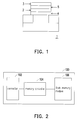
- FIG. 1 is a schematic diagram illustrating a flash memory device according to conventional art.
- a flash memory device 1 includes a charge trapping layer 2 for storing electrons, a control gate 3 for applying voltages, a tunnel oxide layer 4 and an interpoly dielectric layer 5 .
- a threshold voltage of the flash memory device 1 may be changed by injecting electrons into the charge trapping layer 2 .
- a digital-level state of the flash memory device 1 is defined to implement a function of storing data.
- a process for injecting the electrons into the charge trapping layer 2 is referred to as a programming process.
- the injected electrons are removed from the charge trapping layer 2 , and then the flash memory device 1 is restored back to a status before programming.
- the flash memory device 1 deteriorates due to the frequent injection and removal of the electrons, thus increasing the speed of injecting the electrons and extending the distribution of the threshold voltage. As a result, after the frequent injection and removal of the electrons, the storage state of the flash memory device 1 is unlikely to be identified accurately, and results in occurrence of error bits.
- the invention is directed to a solid state storage device and a sensing voltage setting method thereof, and capable of accurately identify a storage state of the memory cell when the memory cell deteriorates.
- the invention provides a sensing voltage setting method of a solid state storage device, and the solid state storage device includes a flash memory module configured to store data.
- the flash memory module has a plurality of memory cells, and each of the memory cells has a first storage state and a second storage state.
- the sensing voltage setting method includes the following steps. First, a predetermined read voltage of the memory cells is adjusted to obtain a plurality of detection read voltages. Next, the predetermined read voltage and the detection read voltages are respectively applied to a plurality of memory cells in order to read a plurality of verification bit data.
- the step of adjusting the predetermined read voltage of the memory cells to obtain the detection read voltages includes: using the predetermined read voltage as a reference for obtaining the detection read voltages according to the predetermined read voltage and a plurality of predetermined intervals, in which a number of the detection read voltages is equal to a number of the predetermined intervals.
- the step of calculating and recording the statistical parametric values between the predetermined read voltage and the detection read voltages adjacent to each other according to the verification bit data corresponding to the predetermined read voltage and the detection read voltages includes: calculating a plurality of variations of bit data identified as in the first storage state among the verification bit data corresponding to the predetermined read voltage and the detection read voltages; calculating and obtaining the statistical parametric values between the predetermined read voltage and the detection read voltages adjacent to each other according to the variations and the predetermined intervals respectively corresponding to the predetermined read voltage and the detection read voltages.
- the method before the step of obtaining the optimized read voltage according to the statistical parametric values, the method further includes: applying an additional detection read voltage to the memory cells, and calculating an additional statistical parametric value between one of the detection read voltages adjacent to the additional detection read voltage and the additional detection read voltage; and recording the additional statistical parametric value as one of the statistical parametric values.
- the step of obtaining the optimized read voltage according to the statistical parametric values includes: establishing a polynomial equation according to the statistical parametric values currently recorded and approximating the statistical parametric values through the polynomial equation; and searching a minimum estimated value according to the polynomial equation and obtaining the optimized read voltage according to the minimum estimated value.
- the method before the step of establishing the polynomial equation according to the statistical parametric values currently recorded and approximating the statistical parametric values through the polynomial equation, the method further includes: determining whether a local minimum can be searched from the statistical parametric values; and if the local minimum cannot be searched from the statistical parametric values, applying an additional detection read voltage to the memory cells to obtain the additional statistical parametric value and record the additional statistical parametric value as one of the statistical parametric values.
- the method before the step of applying the additional detection read voltage to the memory cells to obtain the additional statistical parametric value and record the additional statistical parametric value as one of the statistical parametric values, the method further includes: determining whether a read number is greater than a predetermined number, in which the read number is a sum of a number of times for applying the detection read voltages and applying the predetermined read voltage to the memory cells and a number of times for applying the additional detection read voltage to the memory cells; and if the read number is greater than the predetermined number, obtaining the optimized read voltage according to the statistical parametric values currently recorded.
- the method further includes: determining whether the polynomial equation and the statistical parametric values are in a normal status according to the polynomial equation and the statistical parametric values; and if the polynomial equation and the statistical parametric values are not in the normal status, applying the additional detection read voltage to the memory cells to obtain the additional statistical parametric value and record the additional statistical parametric value as one of the statistical parametric values.
- the sensing voltage setting method further includes: determining whether the statistical parametric values are in a first shifting status or in a second shifting status according to a parametric model; when the statistical parametric values are in the first shifting status, selecting the additional detection read voltage greater than the predetermined read voltage; and when the statistical parametric values are in the second shifting status, selecting the additional detection read voltage less than the predetermined read voltage.
- the invention provides a solid state storage device, which includes a flash memory module and a memory controller.
- the flash memory module has a plurality of memory cells, and each of the memory cells has a first storage state and a second storage state.
- the memory controller is coupled to the flash memory module, and the memory controller is configured to adjust a predetermined read voltage of the memory cells to obtain a plurality of detection read voltages.
- the memory controller is further configured to apply the predetermined read voltage and the detection read voltages respectively to the memory cells to read a plurality of verification bit data corresponding to the predetermined read voltage and the detection read voltages.
- the memory controller is further configured to calculate and record a plurality of statistical parametric values between the predetermined read voltage and the detection read voltages adjacent to each other according to the verification bit data corresponding to the predetermined read voltage and the detection read voltages.
- the memory controller is further configured to obtain an optimized read voltage according to the statistical parametric values.
- the solid state storage device and the sensing voltage setting method thereof are capable of adjusting the predetermined read voltage by using the appropriate detection read voltages based on the threshold voltage distribution of the memory cells.
- the storage state of the memory cell may be correctly identified, so as to avoid loss of data stored in the memory cell.
- FIG. 1 is a schematic diagram illustrating a flash memory device according to conventional art.
- FIG. 2 is a schematic block diagram illustrating a memory storage device according to an exemplary embodiment.
- FIG. 3 is a schematic block diagram illustrating a flash memory module according to an exemplary embodiment.
- FIG. 4 is a schematic diagram illustrating a memory cell array according to an exemplary embodiment.
- FIG. 5 is a schematic diagram illustrating a relation between the storage states and the threshold voltages in the flash memory module according to an exemplary embodiment.
- FIG. 6A to FIG. 6C are other schematic diagrams illustrating a relation between the storage states and the threshold voltages in the flash memory module according to an exemplary embodiment.
- FIG. 7 is a flowchart illustrating a sensing voltage setting method according to an embodiment of the invention.
- FIG. 8 is a schematic diagram illustrating a relation between the variations and the threshold voltages according to an embodiment of the invention.
- FIG. 9 is a schematic diagram illustrating a relation between the statistical parametric values and the threshold voltages according to an embodiment of the invention.
- FIG. 10 is a schematic diagram illustrating a relation between the variations and the threshold voltages according to an embodiment of the invention.
- FIG. 11 is a schematic diagram illustrating a relation between the statistical parametric values and the threshold voltages according to an embodiment of the invention.
- a solid state storage device includes a flash memory module and a memory controller.
- the solid state storage device is usually used together with a host system so that the host system may write data to or read data from the solid state storage device.
- FIG. 2 is a schematic block diagram illustrating a solid state storage device according to an exemplary embodiment.
- a solid state storage device 100 includes a connector 102 , a memory controller 104 , and a flash memory module 106 .
- the connector 102 is compatible with a Universal Serial Bus (USB) interface.
- USB Universal Serial Bus
- the invention is not limited thereto, and the connector 102 may also be compatible with a Parallel Advanced Technology Attachment (PATA) standard, an Institute of Electrical and Electronic Engineers (IEEE) 1394 standard, a Peripheral Component Interconnect Express (PCI Express) interface standard, a Secure Digital (SD) interface standard, a Serial Advanced Technology Attachment (SATA) standard, a Memory Stick (MS) interface standard, a Multi Media Card (MMC) interface standard, an embedded MMC (eMMC) interface standard, a Universal Flash Storage (UFS) interface standard, a Compact Flash (CF) interface standard, an Integrated Device Electronics (IDE) interface standard or other suitable standards.
- PATA Parallel Advanced Technology Attachment
- IEEE 1394 Peripheral Component Interconnect Express
- SD Serial Advanced Technology Attachment
- MS Memory Stick
- MMC Multi Media Card
- UFS Universal Flash Storage
- CF Compact Flash
- IDE Integrated Device Electronics
- the memory controller 104 is used to execute a plurality of logic gates or control commands which are implemented in a hardware form or in a firmware form, so as to perform operations of writing, reading or erasing data in the flash memory module 106 according to the commands of the host system.
- the flash memory module 106 is coupled to the memory controller 104 and configured to store the data written by the host system.
- the flash memory module 106 may be a Single Level Cell (SLC) NAND flash memory module (i.e., a flash memory module capable of storing one bit data in one memory cell), a Multi Level Cell (MLC) NAND flash memory module (i.e., a flash memory module capable of storing two bit data in one memory cell), a Trinary Level Cell (TLC) NAND flash memory module (i.e., a flash memory module capable of storing three bit data in one memory cell), other flash memory modules or any memory module having the same features.
- SLC Single Level Cell
- MLC Multi Level Cell
- TLC Trinary Level Cell
- FIG. 3 is a schematic block diagram illustrating a flash memory module according to an exemplary embodiment.
- the flash memory module 106 includes a memory cell array 2202 , a word line control circuit 2204 , a bit line control circuit 2206 , a column decoder 2208 , a data input-output buffer 2210 and a control circuit 2212 .
- FIG. 4 is a schematic diagram illustrating a memory cell array according to an exemplary embodiment.
- the memory cell array 2202 includes a plurality of memory cells 702 used to store data, a plurality of select gate drain (SGD) transistors 712 , a plurality of select gate source (SGS) transistors 714 , as well as a plurality of bit lines 704 , a plurality of word lines 706 , a common source line 708 connected to the memory cells.
- the memory cells 702 are disposed at intersections of the bit lines 704 and the word lines 706 in arrays.
- the control circuit 2212 controls the word line control circuit 2204 , the bit line control circuit 2206 , the column decoder 2208 , the data input-output buffer 2210 to write the data in the memory cell array 2202 or read the data from the memory cell array 2202 .
- the word line control circuit 2204 is configured to control voltages applied to the word lines 706 ;
- the bit line control circuit 2206 is configured to control voltages applied to the bit lines 704 ;
- the column decoder 2208 is configured to select the corresponding bit line according to a decoding row address in a command; and the data input-output buffer 2210 is configured to temporarily store the data.
- the bit data stored in the memory cells in the flash memory module 106 are represented by a gate threshold voltage. More specifically, each of the memory cells in the memory array 2022 has a plurality of storage states, and the storage states are differentiated according a plurality of predetermined read voltages when reading the data.
- FIG. 5 is a schematic diagram illustrating a relation between the storage states and the read voltages in the flash memory module according to an exemplary embodiment.
- the threshold voltage of each of the memory cells may be differentiated into four storage states according to a first predetermined read voltage VA, a second predetermined read voltage VB and a third predetermined read voltage VA, and bit data “11”, “10”, “00” and “01” are represented by the storage states, respectively.
- each of the storage states includes a least significant bit (LSB) and a most significant bit (MSB).
- LSB least significant bit
- MSB most significant bit
- each of the memory cells may store two bit data.
- each of the memory cells includes four storage states, and the four storage states are the threshold voltages being differentiated by using the three predetermined read voltages.
- the storage states corresponding to the threshold voltages as illustrated in the FIG. 5 are merely an example and are not intended to limit the scope of the invention.
- the storage states corresponding to the read voltages may also have an arrangement of “11”, “10”, “01” and “00” that is arranged according to the threshold voltages from small to large.
- FIG. 6A to FIG. 6C are schematic diagrams illustrating a relation between the storage states and the read voltages in the flash memory module according to an exemplary embodiment.
- the bit data stored in the memory cells are represented by the threshold voltages.
- the memory controller 104 issues a read command to the flash memory module 106 .
- a control circuit 2212 of the flash memory module 106 applies the predetermined read voltage to the word line connected to the memory cells to be read, so as to verify the storage states of the memory cells. As shown in FIG.
- a predetermined read voltage VR may be used to identify whether the bit data stored in the memory cells are in the storage state “A” or the storage state “B”.
- the control circuit 2212 applies the predetermined read voltage VR to the memory cells intended to be read, the memory cells being turned on are identified as in the storage state “A”, and the memory cells not being turned on are identified as in the storage state “B”, such that the bit data stored in the memory cells may then be informed of
- a part of structures in the memory cells 702 of the flash memory module 106 may be deteriorated (e.g., the tunnel oxide layer may be deteriorated) due to the frequent injection and removal of the electrons.
- the threshold voltages of the memory cells 702 may shift as the electrons are injected and removed repeatedly (as illustrated in dash lines of FIG. 6B ), and result in that the storage states of the memory cells are unlikely to be identified accurately by the predetermined read voltage VR.
- a slash area Z_ 1 represents the occurrence of inaccurate determination when using the predetermined read voltage VR.
- the memory cells in the slash area Z_ 1 are supposed to be identified as in the storage state “A”, but the threshold voltages have already been shifted by the frequent injection and removal of the electrons, such that the memory cells are determined as in the storage state “B” based on the predetermined read voltage VR.
- the invention may adaptively adjust the read voltage for identifying the storage states to further improve accuracy in accessing data in the solid state storage device.
- the memory controller 104 may estimate an ideal read voltage VR _ 1 (as shown in FIG. 6C ) suitable for the threshold voltage distribution being shifted in the present embodiment.
- the ideal read voltage VR_ 1 is used to identify the memory cells as in the storage state “A” or in the storage state “B”, in comparison to the slash region Z_ 1 depicted in FIG.
- a slash region Z_ 2 depicted in FIG. 6C where the data may be identified inaccurately is relatively smaller.
- a probability for identifying the data inaccurately may be lowered by using the ideal read voltage VR_ 1 for reading the data.
- FIG. 7 is a flowchart illustrating a sensing voltage setting method of a solid state storage device according to an embodiment of the invention.
- a method of the present embodiment is adapted to the solid state storage device 100 as described above. Detailed steps in the method of the present embodiment are described as below, with reference to each elements of the solid state storage device 100 depicted in FIG. 2 .
- the memory controller 104 may set a plurality of detection read voltages according to the predetermined read voltage for reading the data from the memory cells, and decide an optimized read voltage according to a statistical data of verification bit data among the data being read.
- the memory controller 104 may program the data into the memory cells of the flash memory module 106 in advance, so as to further decide the optimized read voltage currently under estimation is going to be used on which two storage states of the read voltages.
- the predetermined read voltage may identify the memory cells stored with the data as in a first storage state or in a second storage state when reading the data.
- the memory controller 104 adjusts a predetermined read voltage of the memory cells to obtain a plurality of detection read voltages.
- the predetermined read voltage is already decided when the flash memory module 106 is designed by a design personnel.
- the predetermined read voltage is the read voltage initially used by the memory controller 104 for reading the data.
- FIG. 8 is a schematic diagram illustrating a relation between the variations and the threshold voltages according to an embodiment of the invention.
- the memory controller 104 may use the predetermined read voltage VR as a reference for obtaining the detection read voltages according to the predetermined read voltage VR and a plurality of predetermined intervals. More specifically, in the embodiment depicted in FIG. 8 , the memory controller 104 uses the predetermined read voltage VR as a center reference point for obtaining the detection read voltages by using a summation and a decrement methods.
- a predetermined interval R 1 is a voltage difference between a detection voltage VD 1 and the predetermined read voltage VR
- a predetermined interval R 2 is a voltage difference between a detection voltage VD 2 and the predetermined read voltage VR.
- a predetermined interval R 3 is a voltage difference between a detection voltage VD 3 and the detection voltage VD 1
- a predetermined interval R 4 is a voltage difference between a detection voltage VD 4 and the detection voltage VD 2 .
- step S 720 the memory controller 104 applies the predetermined read voltage VR and the detection read voltages VD 1 to VD 4 respectively to the memory cells to read a plurality of verification bit data corresponding to the predetermined read voltage VR and the detection read voltages VD 1 to VD 4 .
- each of the verification bit data obtained after reading by the memory controller 104 using the predetermined read voltage VR and the detection read voltages VD 1 to VD 4 are different from one another.
- step S 730 the memory controller 104 calculates and records a plurality of statistical parametric values between the predetermined read voltage and the detection read voltages adjacent to each other according to the verification bit data corresponding to the predetermined read voltage VR and the detection read voltages VD 1 to VD 4 .
- the memory controller 104 obtains a plurality of different verification bit data by using different voltages, and obtains the statistical parametric values between the predetermined read voltage and the detection read voltages adjacent to each other according to information provided by the verification bit data.
- step S 730 includes steps S 731 and S 732 .
- step S 731 the memory controller 104 calculates a plurality of variations V 1 to V 5 of bit data identified as in the first storage state among the verification bit data corresponding to the predetermined read voltage VR and the detection read voltages VD 1 to VD 4 .
- the variations may represent a degree and a condition of shifting in the threshold voltage distribution, and a unit used therein is a number of the memory cells.
- the memory control 104 may program detection data into the memory cells and apply the predetermined read voltage VR and the detection read voltages VD 1 to VD 4 memory to read a plurality of initial verification bit data and calculate a number of the bit data identified as in the first storage state among the initial verification bit data. Information regarding the number of the bit data identified as in the first storage state among the initial verification bit data corresponding to the predetermined read voltage VR and the detection read voltages VD 1 to VD 4 are recorded.
- the memory controller 104 may calculate the number of the bit data currently identified as in the first storage state among the verification bit data corresponding to the predetermined read voltage VR and the detection read voltages VD 1 to VD 4 .
- the memory controller 104 may subtract the number of the bit data identified as in the first storage state among the verification bit data obtained by using the predetermined read voltage VR and the detection read voltages VD 1 to VD 4 by the number of the bit data identified as in the first storage state among the corresponding initial verification bit data.
- the variations of the bit data identified as in the first storage state may be obtained. Based on the above, it can be known that in case the different read voltages are applied, the different verification bit data may be read.
- the memory controller 104 may obtain the variations of the predetermined read voltage VR and the detection read voltages VD 1 to VD 4 according to the initial verification bit data and the verification bit data of each of the predetermined read voltage VR and the detection read voltages VD 1 to VD 4 .
- a curve L depicted FIG. 8 represents the variations corresponding to the different read voltages.
- the memory controller 104 may not calculate the variations corresponding to all of the read voltages one by one but only obtain the variations V 1 to V 5 corresponding to the predetermined read voltage VR and the detection read voltages VD 1 to VD 4 . As shown in FIG.
- the predetermined read voltage VR is corresponding to the variation V 1 ; the detection read voltage VD 1 is corresponding to the variation V 2 ; the detection read voltage VD 2 is corresponding to the variation V 3 ; the detection read voltage VD 3 is corresponding to the variation V 4 ; and the detection read voltage VD 4 is corresponding to the variation V 5 .
- the memory controller 104 may calculate and obtain statistical parametric values between the predetermined read voltage VR and the detection read voltages VD 1 to VD 4 adjacent to each other according to the voltage ranges of the variations V 1 to V 5 and the predetermined intervals R 1 to R 4 respectively corresponding to the predetermined read voltage VR and the detection read voltages VD 1 to VD 4 .
- FIG. 9 is a schematic diagram illustrating a relation between the statistical parametric values and the threshold voltages according to an embodiment of the invention. Referring to FIG. 8 and FIG.
- statistical parametric values S 1 to S 4 between the predetermined read voltage VR and the detection read voltages VD 1 to VD 4 adjacent to each other are obtained by calculating an area of a region corresponding to two variations in each of the predetermined intervals R 1 to R 4 .
- the statistical parametric value S 1 between the predetermined read voltage VR and the detection read voltage VD 1 is equal to an area of a region al (a slash region depicted in FIG. 8 ) corresponding to the variation V 1 , the variation V 2 and the predetermined interval R 1 .
- the memory controller 104 may also obtain the statistical parametric values S 2 to S 4 by calculating areas of regions. More specifically, the statistical parametric values S 1 to S 4 may represent the number of memory cells having the threshold voltage that falls within each of the predetermined intervals R 1 to R 4 , respectively. For instance, the statistical parametric value S 1 may be referred to as the number of the memory cells having the threshold voltage that falls between predetermined read voltage VR and the detection read voltage VD 1 . As shown in FIG.
- the statistical parametric value S 1 is provided between the predetermined read voltage VR and the detection read voltage VD 1 ; the statistical parametric value S 2 is provided between the predetermined read voltage VR and the detection read voltage VD 2 ; the statistical parametric value S 3 is provided between the detection read voltage VD 1 and the detection read voltage VD 3 ; and the statistical parametric value S 4 is provided between the detection read voltage VD 2 and the detection read voltage VD 4 .
- the memory controller 104 may determine whether the optimized read voltage can be searched from the statistical parametric values currently recorded by using other mechanisms.
- step S 740 the memory controller 104 determines whether a local minimum can be searched from the statistical parametric values.
- the memory controller 104 determines whether a local minimum can be searched from the statistical parametric values.
- the current statistical parametric values S 1 to S 4 are gradually increased along with increases in the threshold voltages, it indicates that the local minimum may not be included in the statistical parametric values currently recorded. Otherwise, it indicates that the local minimum may have included in the statistical parametric values currently recorded, such that the memory controller 104 may obtain the optimized read voltage in subsequent processes according to the local minimum included in the statistical parametric values.
- step S 740 determines whether a read number is greater than a predetermined number.
- the read number is a sum of a number of times for applying the detection read voltages and the predetermined read voltage to the memory cells and a number of times for applying the additional detection read voltage to the memory cells (i.e., a number of times for the memory controller 104 to read the data).
- the memory controller 104 stops reading and applying the additional detection read voltage. Accordingly, proceeding back to step S 750 in which the memory controller 104 obtains the optimized read voltage according to the statistical parametric values currently recorded. If the read number is not greater than the predetermined number, in step S 770 , the memory controller 104 applies an additional detection read voltage to the memory cells, and calculates an additional statistical parametric value between one of the detection read voltages adjacent to the additional detection read voltage and the additional detection read voltage.
- FIG. 10 is a schematic diagram illustrating a relation between the variations and the threshold voltages according to an embodiment of the invention.
- the memory controller 104 obtains the detection read voltage VD 5 according to the voltage range of the predetermined interval R 5 , and applies the detection read voltage VD 5 to perform a sixth read, so as to obtain a variation V 6 corresponding to the detection read voltage VD 5 .
- the voltage range of the predetermined interval R 5 may be identical to or different from that of the predetermined intervals R 1 to R 4 depended on the actual applications.
- an area of a region a 2 may be obtained by the memory controller 104 according to the voltage ranges of the variation V 5 , the variation V 6 and the predetermined interval R 5 .
- an additional statistical parametric value S 5 may be obtained by the memory controller 104 according to the voltage ranges of the variation V 5 , the variation V 6 and the predetermined interval R 5 .
- step S 780 the memory controller 104 records the additional statistical parametric value as one of the statistical parametric values.
- FIG. 11 is a schematic diagram illustrating a relation between the variations and the threshold voltages according to an embodiment of the invention. Referring to FIG. 11 , the memory controller 104 adds the additional statistical parametric value S 5 into the statistical parametric values S 1 to S 4 already being recorded. Hence, all of the statistical parametric values S 1 to S 5 are not only simply gradually increased or gradually decreased along with increases in the threshold voltages. This indicates that the local minimum may be searched from the statistical parametric values S 1 to S 5 by the memory controller 104 without reading again for obtaining the additional statistical parametric value.
- step S 750 includes steps S 751 to S 753 .
- the memory controller 104 establishes a polynomial equation according to the statistical parametric values currently recorded and approximates the statistical parametric values through the polynomial equation. For instance, as shown in FIG. 11 , the memory controller 104 may establish a quadratic function (as shown in a dash line M in FIG. 11 ) according to the statistical parametric values currently recorded, but the invention is not limited thereto.
- step S 752 the memory controller 104 determines whether the polynomial equation and the statistical parametric values are in a normal status according to the polynomial equation and the statistical parametric values.
- the memory controller 104 may obtain the polynomial equation which cannot accurately approximate other statistical parametric values due to said error value. Accordingly, the memory controller 104 may, for example, determine whether the polynomial equation and the statistical parametric values are in the normal status (indicating a real situation) by calculating a root-mean-square error of all the statistical parametric values and the polynomial equation. If the determination in step S 752 is no, proceeding to step S 770 in which the memory controller 104 applies an additional detection read voltage to the memory cells, and calculates an additional statistical parametric value between one of the detection read voltages adjacent to the additional detection read voltage and the additional detection read voltage.
- step S 752 determines whether the determination in step S 752 is yes. If the determination in step S 752 is yes, proceeding to step S 753 in which the memory controller 104 searches a minimum estimated value of the polynomial equation and obtains the optimized read voltage according to the minimum estimated value. For instance, as shown in FIG. 11 , a minimum estimated value Smin (a lowest point at the dash line M) of the quadratic function M may be searched by the memory controller 104 , and an optimized read voltage Vest may be obtained according to the minimum estimated value Smin.
- a minimum estimated value Smin a lowest point at the dash line M
- an optimized read voltage Vest may be obtained according to the minimum estimated value Smin.
- the memory controller 104 may estimate a statistical amount of the current memory cells having the threshold voltage that falls within each of the predetermined interval R 1 to R 5 , and further estimate the optimized read voltage Vest according to above-said information. Accordingly, the memory controller 104 may lower a bit error rate when reading the data by using the optimized read voltage Vest.
- the memory controller 104 may also use other parameter information for deciding the optimized read voltage. More specifically, in the present embodiment, the memory controller 104 may determine whether the statistical parametric values are in a first shifting status or in a second shifting status according to a parametric model. Accordingly, the additional detection read voltage being greater than or less than the predetermined read voltage may be selected. Therein, the parametric model may be established based on experiments or simulations being performed in advance. For instance, according to a gradient of a connection between statistical parametric values and the parametric model established in advance, the memory controller 104 may be known of whether the optimized read voltage is shifted towards a direction to be greater than the predetermined read voltage or shifted towards a direction to be less than the predetermined read voltage. As shown in FIG.
- a gradient between the statistical parametric value S 1 and the statistical parametric value S 2 is positive, and a gradient between the statistical parametric value S 3 and the statistical parametric value S 2 is also positive. Accordingly, it can be known that the optimized read voltage is shift towards the direction to be less than the predetermined read voltage.
- the solid state storage device and the sensing voltage setting method thereof according to the invention are capable of dynamically adjust the read voltages appropriately, so as to avoid loss of the data.
- the optimized read voltage may be obtained by applying a small amount of the detection voltages in the invention, so that the optimized read voltage may be implemented in actual applications more easily.
- the optimized read voltage may be obtained simply by using 4 to 5 of the detection voltages.
- the solid state storage device may identify the stored data by using the optimized read voltage, so as to lower the bit error rate when reading the data.
Abstract
Description
Claims (18)
Applications Claiming Priority (3)
| Application Number | Priority Date | Filing Date | Title |
|---|---|---|---|
| CN201310542369 | 2013-11-05 | ||
| CN201310542369.0 | 2013-11-05 | ||
| CN201310542369.0A CN104616695B (en) | 2013-11-05 | 2013-11-05 | Solid-state storage device and its reading voltage setting method |
Publications (2)
| Publication Number | Publication Date |
|---|---|
| US20150124533A1 US20150124533A1 (en) | 2015-05-07 |
| US9129698B2 true US9129698B2 (en) | 2015-09-08 |
Family
ID=53006922
Family Applications (1)
| Application Number | Title | Priority Date | Filing Date |
|---|---|---|---|
| US14/160,566 Active 2034-05-01 US9129698B2 (en) | 2013-11-05 | 2014-01-22 | Solid state storage device and sensing voltage setting method thereof |
Country Status (2)
| Country | Link |
|---|---|
| US (1) | US9129698B2 (en) |
| CN (1) | CN104616695B (en) |
Cited By (9)
| Publication number | Priority date | Publication date | Assignee | Title |
|---|---|---|---|---|
| US9812210B2 (en) * | 2016-03-16 | 2017-11-07 | Lite-On Electronics (Guangzhou) Limited | Power off period estimating method for solid state storage device |
| US10613795B2 (en) | 2017-09-19 | 2020-04-07 | Samsung Electronics Co., Ltd. | Pre-processing system, method processing characteristic data, and memory control system using same |
| US11029890B1 (en) | 2020-03-02 | 2021-06-08 | Micron Technology, Inc. | Compound feature generation in classification of error rate of data retrieved from memory cells |
| US11081200B1 (en) * | 2020-05-07 | 2021-08-03 | Micron Technology, Inc. | Intelligent proactive responses to operations to read data from memory cells |
| US11086572B1 (en) | 2020-03-02 | 2021-08-10 | Micron Technology, Inc. | Self adapting iterative read calibration to retrieve data from memory cells |
| US11221800B2 (en) | 2020-03-02 | 2022-01-11 | Micron Technology, Inc. | Adaptive and/or iterative operations in executing a read command to retrieve data from memory cells |
| US11257546B2 (en) | 2020-05-07 | 2022-02-22 | Micron Technology, Inc. | Reading of soft bits and hard bits from memory cells |
| US11562793B2 (en) | 2020-05-07 | 2023-01-24 | Micron Technology, Inc. | Read soft bits through boosted modulation following reading hard bits |
| US11740970B2 (en) | 2020-03-02 | 2023-08-29 | Micron Technology, Inc. | Dynamic adjustment of data integrity operations of a memory system based on error rate classification |
Families Citing this family (13)
| Publication number | Priority date | Publication date | Assignee | Title |
|---|---|---|---|---|
| CN107025940B (en) * | 2016-01-19 | 2020-11-20 | 威盛电子股份有限公司 | Nonvolatile memory device and real-time adaptive read voltage adjustment method thereof |
| KR102500616B1 (en) * | 2016-02-26 | 2023-02-17 | 에스케이하이닉스 주식회사 | Data storage device and operating method thereof |
| CN107331420A (en) * | 2016-04-28 | 2017-11-07 | 大心电子股份有限公司 | Coding/decoding method, memory storage apparatus and memorizer control circuit unit |
| CN109065092B (en) * | 2017-02-21 | 2022-06-17 | 北京忆恒创源科技股份有限公司 | Method and device for setting reading threshold of NVM (non-volatile memory) chip |
| CN107527644B (en) * | 2017-08-28 | 2020-07-28 | 苏州浪潮智能科技有限公司 | Method and device for optimizing read reference voltage of solid state disk |
| CN109584935A (en) * | 2017-09-29 | 2019-04-05 | 大心电子(英属维京群岛)股份有限公司 | Method for reading data and storage control |
| CN108133730B (en) * | 2017-12-22 | 2020-09-11 | 联芸科技(杭州)有限公司 | Reading control method of flash memory, memory reading device and memory system |
| TWI651721B (en) | 2018-03-09 | 2019-02-21 | 大陸商深圳大心電子科技有限公司 | Decoding method and storage controller |
| KR102470726B1 (en) * | 2018-03-14 | 2022-11-25 | 삼성전자주식회사 | Non-volatile memory device |
| TWI651726B (en) * | 2018-03-30 | 2019-02-21 | 大陸商深圳大心電子科技有限公司 | Decoding method and storage controller |
| TWI661427B (en) | 2018-04-02 | 2019-06-01 | 大陸商深圳大心電子科技有限公司 | Memory management method and storage controller |
| CN110767253B (en) * | 2018-07-25 | 2021-08-03 | 建兴储存科技(广州)有限公司 | Solid state storage device and read table management method thereof |
| US11244729B1 (en) * | 2020-08-07 | 2022-02-08 | Micron Technology, Inc. | Search for an optimized read voltage |
Citations (2)
| Publication number | Priority date | Publication date | Assignee | Title |
|---|---|---|---|---|
| US20080123420A1 (en) * | 2006-11-03 | 2008-05-29 | Yigal Brandman | Nonvolatile Memory With Variable Read Threshold |
| US8661184B2 (en) * | 2010-01-27 | 2014-02-25 | Fusion-Io, Inc. | Managing non-volatile media |
Family Cites Families (3)
| Publication number | Priority date | Publication date | Assignee | Title |
|---|---|---|---|---|
| KR100888842B1 (en) * | 2007-06-28 | 2009-03-17 | 삼성전자주식회사 | Flash memory device optimizing read voltage and method for optimizing read voltage thereof |
| KR101642465B1 (en) * | 2008-12-12 | 2016-07-25 | 삼성전자주식회사 | Access method of non-volatile memory device |
| KR101578511B1 (en) * | 2009-05-20 | 2015-12-18 | 삼성전자주식회사 | Method for setting a read voltage |
-
2013
- 2013-11-05 CN CN201310542369.0A patent/CN104616695B/en active Active
-
2014
- 2014-01-22 US US14/160,566 patent/US9129698B2/en active Active
Patent Citations (2)
| Publication number | Priority date | Publication date | Assignee | Title |
|---|---|---|---|---|
| US20080123420A1 (en) * | 2006-11-03 | 2008-05-29 | Yigal Brandman | Nonvolatile Memory With Variable Read Threshold |
| US8661184B2 (en) * | 2010-01-27 | 2014-02-25 | Fusion-Io, Inc. | Managing non-volatile media |
Cited By (15)
| Publication number | Priority date | Publication date | Assignee | Title |
|---|---|---|---|---|
| US9812210B2 (en) * | 2016-03-16 | 2017-11-07 | Lite-On Electronics (Guangzhou) Limited | Power off period estimating method for solid state storage device |
| US10613795B2 (en) | 2017-09-19 | 2020-04-07 | Samsung Electronics Co., Ltd. | Pre-processing system, method processing characteristic data, and memory control system using same |
| US11726719B2 (en) | 2020-03-02 | 2023-08-15 | Micron Technology, Inc. | Compound feature generation in classification of error rate of data retrieved from memory cells |
| US11029890B1 (en) | 2020-03-02 | 2021-06-08 | Micron Technology, Inc. | Compound feature generation in classification of error rate of data retrieved from memory cells |
| US11775217B2 (en) | 2020-03-02 | 2023-10-03 | Micron Technology, Inc. | Adaptive and/or iterative operations in executing a read command to retrieve data from memory cells |
| US11086572B1 (en) | 2020-03-02 | 2021-08-10 | Micron Technology, Inc. | Self adapting iterative read calibration to retrieve data from memory cells |
| US11221800B2 (en) | 2020-03-02 | 2022-01-11 | Micron Technology, Inc. | Adaptive and/or iterative operations in executing a read command to retrieve data from memory cells |
| US11403042B2 (en) | 2020-03-02 | 2022-08-02 | Micron Technology, Inc. | Self adapting iterative read calibration to retrieve data from memory cells |
| US11474748B2 (en) | 2020-03-02 | 2022-10-18 | Micron Technology, Inc. | Compound feature generation in classification of error rate of data retrieved from memory cells |
| US11762599B2 (en) | 2020-03-02 | 2023-09-19 | Micron Technology, Inc. | Self adapting iterative read calibration to retrieve data from memory cells |
| US11740970B2 (en) | 2020-03-02 | 2023-08-29 | Micron Technology, Inc. | Dynamic adjustment of data integrity operations of a memory system based on error rate classification |
| US11257546B2 (en) | 2020-05-07 | 2022-02-22 | Micron Technology, Inc. | Reading of soft bits and hard bits from memory cells |
| US11657886B2 (en) | 2020-05-07 | 2023-05-23 | Micron Technology, Inc. | Intelligent proactive responses to operations to read data from memory cells |
| US11562793B2 (en) | 2020-05-07 | 2023-01-24 | Micron Technology, Inc. | Read soft bits through boosted modulation following reading hard bits |
| US11081200B1 (en) * | 2020-05-07 | 2021-08-03 | Micron Technology, Inc. | Intelligent proactive responses to operations to read data from memory cells |
Also Published As
| Publication number | Publication date |
|---|---|
| CN104616695B (en) | 2017-12-22 |
| CN104616695A (en) | 2015-05-13 |
| US20150124533A1 (en) | 2015-05-07 |
Similar Documents
| Publication | Publication Date | Title |
|---|---|---|
| US9129698B2 (en) | Solid state storage device and sensing voltage setting method thereof | |
| TWI521513B (en) | Data reading method, and control circuit, and memory storage apparatus using the same | |
| US9019770B2 (en) | Data reading method, and control circuit, memory module and memory storage apparatus and memory module using the same | |
| US8386860B2 (en) | Methods of calculating compensation voltage and adjusting threshold voltage and memory apparatus and controller | |
| US9286986B2 (en) | Data writing method, and memory control circuit unit and memory storage apparatus using the same | |
| US10930358B2 (en) | Memory system and method of operating the same | |
| TWI541810B (en) | Data writing method, and memory controller and memory storage apparatus using the same | |
| US9257187B2 (en) | Data storing method, memory control circuit unit and memory storage apparatus | |
| US8737126B2 (en) | Data writing method, and memory controller and memory storage apparatus using the same | |
| US9830219B2 (en) | Encoding scheme for 3D vertical flash memory | |
| US9563508B2 (en) | Memory management method, memory control circuit unit and memory storage apparatus | |
| KR20150121835A (en) | Data decoding method of Non-volatile memory device | |
| US8972653B2 (en) | Memory management method, and memory controller and memory storage apparatus using the same | |
| US8830750B1 (en) | Data reading method, and control circuit, memory module and memory storage apparatus using the same | |
| US20150106667A1 (en) | Solid state storage device and controlling method thereof | |
| CN108428467B (en) | Read voltage tracking method, memory storage device and control circuit unit | |
| US20140050024A1 (en) | Data reading method, and circuit, rewritable non-volatile memory module and memory storage apparatus using the same | |
| TWI521525B (en) | Time estimating method, memory storage device, and memory controlling circuit unit | |
| US11887680B2 (en) | Reducing program verifies for multi-level NAND cells | |
| CN104679441A (en) | Time estimation method, memory storage device and memory control circuit unit | |
| US11941271B2 (en) | Storage devices performing secure erase and operating methods thereof | |
| US20230343401A1 (en) | Nonvolatile memory device, memory system, and programming method |
Legal Events
| Date | Code | Title | Description |
|---|---|---|---|
| AS | Assignment |
Owner name: LITE-ON IT CORPORATION, TAIWAN Free format text: ASSIGNMENT OF ASSIGNORS INTEREST;ASSIGNORS:ZENG, SHIH-JIA;FU, JEN-CHIEN;WU, YU-SHAN;AND OTHERS;SIGNING DATES FROM 20131226 TO 20140102;REEL/FRAME:032034/0137 |
|
| AS | Assignment |
Owner name: LITE-ON TECHNOLOGY CORPORATION, TAIWAN Free format text: ASSIGNMENT OF ASSIGNORS INTEREST;ASSIGNOR:LITE-ON IT CORP.;REEL/FRAME:032892/0554 Effective date: 20140512 |
|
| STCF | Information on status: patent grant |
Free format text: PATENTED CASE |
|
| MAFP | Maintenance fee payment |
Free format text: PAYMENT OF MAINTENANCE FEE, 4TH YEAR, LARGE ENTITY (ORIGINAL EVENT CODE: M1551); ENTITY STATUS OF PATENT OWNER: LARGE ENTITY Year of fee payment: 4 |
|
| AS | Assignment |
Owner name: SOLID STATE STORAGE TECHNOLOGY CORPORATION, TAIWAN Free format text: ASSIGNMENT OF ASSIGNORS INTEREST;ASSIGNOR:LITE-ON TECHNOLOGY CORPORATION;REEL/FRAME:051213/0875 Effective date: 20191204 |
|
| MAFP | Maintenance fee payment |
Free format text: PAYMENT OF MAINTENANCE FEE, 8TH YEAR, LARGE ENTITY (ORIGINAL EVENT CODE: M1552); ENTITY STATUS OF PATENT OWNER: LARGE ENTITY Year of fee payment: 8 |