US9151827B2 - Compensating slowly varying if DC offsets in receivers - Google Patents
Compensating slowly varying if DC offsets in receivers Download PDFInfo
- Publication number
- US9151827B2 US9151827B2 US13/710,963 US201213710963A US9151827B2 US 9151827 B2 US9151827 B2 US 9151827B2 US 201213710963 A US201213710963 A US 201213710963A US 9151827 B2 US9151827 B2 US 9151827B2
- Authority
- US
- United States
- Prior art keywords
- signal
- generate
- compensation parameters
- correction
- partial sum
- Prior art date
- Legal status (The legal status is an assumption and is not a legal conclusion. Google has not performed a legal analysis and makes no representation as to the accuracy of the status listed.)
- Active, expires
Links
Images


Classifications
-
- G—PHYSICS
- G01—MEASURING; TESTING
- G01S—RADIO DIRECTION-FINDING; RADIO NAVIGATION; DETERMINING DISTANCE OR VELOCITY BY USE OF RADIO WAVES; LOCATING OR PRESENCE-DETECTING BY USE OF THE REFLECTION OR RERADIATION OF RADIO WAVES; ANALOGOUS ARRANGEMENTS USING OTHER WAVES
- G01S7/00—Details of systems according to groups G01S13/00, G01S15/00, G01S17/00
- G01S7/02—Details of systems according to groups G01S13/00, G01S15/00, G01S17/00 of systems according to group G01S13/00
- G01S7/35—Details of non-pulse systems
- G01S7/352—Receivers
- G01S7/354—Extracting wanted echo-signals
-
- G—PHYSICS
- G01—MEASURING; TESTING
- G01S—RADIO DIRECTION-FINDING; RADIO NAVIGATION; DETERMINING DISTANCE OR VELOCITY BY USE OF RADIO WAVES; LOCATING OR PRESENCE-DETECTING BY USE OF THE REFLECTION OR RERADIATION OF RADIO WAVES; ANALOGOUS ARRANGEMENTS USING OTHER WAVES
- G01S13/00—Systems using the reflection or reradiation of radio waves, e.g. radar systems; Analogous systems using reflection or reradiation of waves whose nature or wavelength is irrelevant or unspecified
- G01S13/02—Systems using reflection of radio waves, e.g. primary radar systems; Analogous systems
- G01S13/06—Systems determining position data of a target
- G01S13/08—Systems for measuring distance only
- G01S13/32—Systems for measuring distance only using transmission of continuous waves, whether amplitude-, frequency-, or phase-modulated, or unmodulated
- G01S13/34—Systems for measuring distance only using transmission of continuous waves, whether amplitude-, frequency-, or phase-modulated, or unmodulated using transmission of continuous, frequency-modulated waves while heterodyning the received signal, or a signal derived therefrom, with a locally-generated signal related to the contemporaneously transmitted signal
- G01S13/343—Systems for measuring distance only using transmission of continuous waves, whether amplitude-, frequency-, or phase-modulated, or unmodulated using transmission of continuous, frequency-modulated waves while heterodyning the received signal, or a signal derived therefrom, with a locally-generated signal related to the contemporaneously transmitted signal using sawtooth modulation
-
- G—PHYSICS
- G01—MEASURING; TESTING
- G01S—RADIO DIRECTION-FINDING; RADIO NAVIGATION; DETERMINING DISTANCE OR VELOCITY BY USE OF RADIO WAVES; LOCATING OR PRESENCE-DETECTING BY USE OF THE REFLECTION OR RERADIATION OF RADIO WAVES; ANALOGOUS ARRANGEMENTS USING OTHER WAVES
- G01S7/00—Details of systems according to groups G01S13/00, G01S15/00, G01S17/00
- G01S7/02—Details of systems according to groups G01S13/00, G01S15/00, G01S17/00 of systems according to group G01S13/00
- G01S7/03—Details of HF subsystems specially adapted therefor, e.g. common to transmitter and receiver
- G01S7/038—Feedthrough nulling circuits
-
- G—PHYSICS
- G01—MEASURING; TESTING
- G01S—RADIO DIRECTION-FINDING; RADIO NAVIGATION; DETERMINING DISTANCE OR VELOCITY BY USE OF RADIO WAVES; LOCATING OR PRESENCE-DETECTING BY USE OF THE REFLECTION OR RERADIATION OF RADIO WAVES; ANALOGOUS ARRANGEMENTS USING OTHER WAVES
- G01S7/00—Details of systems according to groups G01S13/00, G01S15/00, G01S17/00
- G01S7/02—Details of systems according to groups G01S13/00, G01S15/00, G01S17/00 of systems according to group G01S13/00
- G01S7/40—Means for monitoring or calibrating
- G01S7/4004—Means for monitoring or calibrating of parts of a radar system
Definitions
- FMCW radar systems are used to wirelessly detect the position of objects through the use of electromagnetic radiation.
- Frequency modulated continuous wave (FMCW) radar systems have become a common type of radar system.
- FMCW radars utilize a signal that continually changes frequency around a fixed reference frequency. Since the frequency of the signal continually changes with time, the frequency of a transmitted signal and a reflected signal will differ by a frequency that is proportional to the round trip time of the signal, giving a distance of a detected object.
- FIG. 1A illustrates a block diagram of a typical FMCW radar system 100 .
- FMCW radar system 100 comprises a transmission path and a reception path.
- a ramped signal generator 102 is configured to generate a ramped signal S ramp that is provided to a transmission chain 104 in the transmission path and a receive mixer 118 in the reception path.
- the transmission chain 104 generates a ramped RF signal that is transmitted as an electromagnetic wave 108 by a transmit antenna 106 .
- Electromagnetic wave 108 reflects off of an object 110 as a reflected wave 112 , which is returned to a reception antenna 114 that provides a reflected signal to a reception chain 116 that down-converts the reflected signal.
- the receive mixer 118 mixes the down-converted signal with the ramped signal S ramp to generate a signal having a frequency proportional to a position of the object 110 , which is provided to a signal processing unit (SPU) 120 .
- SPU signal processing unit
- FIG. 1B illustrates a timing diagram 122 showing operation of FMCW radar system 100 .
- a transmitted signal 124 has a continually varying linear frequency ramp with a sawtooth waveform
- a reflected signal 126 has a continually varying linear frequency ramp with a sawtooth waveform that is offset in time from transmitted signal 124 by a round-trip time t rt (corresponding to a frequency difference).
- FIG. 1A is a block diagram of a FMCW (frequency modulated continuous wave) radar system.
- FIG. 1B is a timing diagram showing operation f the FMCW of FIG. 1A .
- FIG. 2 is a block diagram of a radar system having a feedback path with a signal correction element.
- FIG. 3 is a block diagram of a FMCW radar system having a feedback path with a signal correction element.
- FIG. 4 is a block diagram of a FMCW radar system having a feedback path with a signal correction element.
- FIGS. 5A-5B illustrate graphs showing the reduction in unwanted low frequency and/or DC signals.
- FIGS. 6A-6B illustrate a FMCW radar system having a feedback path comprising an analog polynomial generator configured to generate a correction signal.
- FIGS. 7A-7B illustrate a FMCW radar system having a feedback path comprising a digital polynomial generator configured to generate a correction signal.
- FIG. 8 is a flow diagram of an exemplary method of reducing offset errors in a sensor signal.
- signal leakage may occur from a transmission path to a reception path when simultaneously operated in close proximity. Such signal leakage may result in unwanted signal components (e.g., DC and/or low frequency components) in a reflected signal that often have a large amplitude.
- the gain of the reception path can be set low. However, setting the gain of the reception path low limits the dynamic range of the reception path.
- high pass filtering or AC coupling can be used to remove the unwanted signal components.
- filtering utilizes large capacitors which take a long time to settle, posing problems when the radar system is operated in a burst or ‘duty cycle’ mode, in which a transmitter is intermittently switched on and off. Setting filter capacitors to have a short time constant (i.e., to settle quickly) will alleviate the long settling time, but filters out useful low frequency signal components from close range targets.
- the transmitter can be switched on earlier (to allow extra time settling time), but switching the transmitter on earlier results in more power consumption and unwanted signal emissions.
- the present disclosure relates to receiver system comprising a feedback path having a signal correction element configured to remove unwanted signal components from a received signal based upon signal information from previous received signals.
- the receiver system comprises a signal generator configured to generate a plurality of signal patterns. One of the plurality of signal patterns is provided to a transmit antenna configured to wirelessly transmit the signal pattern.
- a receive antenna port is configured to receive a reflected signal comprising a time-shifted version of the signal pattern and to provide the reflected signal to a reception path.
- a feedback path extends from the reception path to a signal correction element configured to selectively generate a correction signal that reduces unwanted signal components in the reflected signal.
- the signal correction element generates the correction signal from compensation parameters stored in a memory, which correspond to previously received reflected signals comprising the signal pattern, so that the correction signal can be used to reduce unwanted signal components in real time.
- FIG. 2 is a block diagram of a radar system 200 having a feedback path with a signal correction element 220 configured to generate a correction signal S cor that removes unwanted signal components from a reflected signal S ref .
- the radar system 200 comprises a signal generator 204 configured to generate a plurality of signal patterns.
- the signal generator 204 provides one of the plurality of signal patterns to a transmit antenna 202 configured to transmit the signal pattern as electromagnetic radiation 206 .
- a receive antenna 212 having a constant coupling with the transmit antenna 202 , is configured to receive a reflected signal 210 comprising a time shifted version of the signal pattern from an object 208 .
- the reflected signal S ref is provided a receive antenna port 214 , a downstream intermediate frequency (IF) signal processing element 218 , and a downstream signal processing unit 224 .
- IF intermediate frequency
- a feedback path extending from an output of the IF signal processing element 218 to a signal correction element 220 , provides a feedback signal S fb to the signal correction element 220 .
- the signal correction element 220 is configured to perform a measurement sweep of the feedback signal S fb and from the measurement sweep to determine one or more compensation parameters corresponding to the received signal pattern.
- the signal correction element 220 comprises a memory element 222 configured to store compensation parameters corresponding to a plurality of signal patterns determined over a plurality of measurement sweeps.
- the signal correction element 220 After the signal correction element 220 has determined compensation parameters corresponding to a signal pattern, the signal correction element is able to generate a correction signal S cor , based upon stored compensation parameters, which reduces unwanted signal components in a reflected signal S ref comprising the signal pattern.
- the correction signal S cor is subtracted from the reflected signal by adder 216 to generate an adjusted signal S adj that has reduced unwanted signal components.
- FIG. 3 is a block diagram of a disclosed FMCW (frequency modulated continuous wave) radar system 300 having a feedback path 316 with a signal correction element 318 configured to generate a correction signal S cor that removes unwanted signal components from a reflected signal S ref .
- FMCW frequency modulated continuous wave
- the FMCW radar system 300 comprises one or more receive antennas 302 configured to receive an electromagnetic signal 306 reflected from an object 304 .
- the one or more receive antennas 302 may comprise a single antenna configured to receive the electromagnetic signal 306 .
- the one or more receive antennas 302 may comprise an antenna array having a plurality of antennas, wherein respective antennas are configured to receive a different frequency channel of the electromagnetic signal 306 .
- the FMCW radar system 300 further comprises a ramped signal generator 320 configured to generate a plurality of ramped signal having a continually varying frequency ramp (e.g., a sawtooth waveform).
- the ramped signal generator 320 is controlled by a transmit system controller 322 that is configured to define one or more parameters of the ramped signals.
- a ramped signal S ramp comprising one of the plurality of ramped signals, is provided to a transmission path TX, which transmit a signal from the FMCW radar system 300 , and to a receive mixer 308 located within the reception path.
- the receive mixer 308 also receives a reflected signal S ref , which is based upon the electromagnetic signal 306 , and mixes the reflected signal S ref with the ramped signal S ramp . Mixing the reflected signal S ref with the ramped signal S ramp provides for a mixed signal S mix having a frequency that is proportional to a distance between the FMCW radar system 300 and the object 304 .
- the mixed signal S mix is provided to an IF signal processing element 310 .
- the IF signal processing element 310 may comprise a modulation element, one or more amplifiers, and one or more filtering elements.
- the IF signal processing element 310 is configured to generate an amplified, down-converted mixed signal S mix ′ that is input to an analog-to-digital converter (ADC) 312 configured to convert the mixed signal S mix ′ from an analog signal to a digital signal.
- ADC analog-to-digital converter
- the digital signal is provided to a digital signal processor 314 configured to process the digital signal to determine a location of the object 304 .
- the amplified, down-converted mixed signal S mix ′ is also provided to a feedback path 316 that provides a feedback signal S fb to a signal correction element 318 .
- the feedback path 316 extends to the signal correction element 318 from a location in the reception path that is downstream of the receive mixer 308 .
- the feedback path 316 may extend from an output of IF signal processing element 310 to the signal correction element 318 .
- the feedback path 316 may extend from an output of ADC 312 to the signal correction element 318 .
- the signal correction element 318 is configured to receive the feedback signal S fb from the feedback path 316 , and a trigger signal S trig from transmit system controller 322 , which indicates a change in the ramped signal S ramp . Based upon the trigger signal S trig and the feedback signal S fb , the signal correction element 318 is configured to determine unwanted signal components of a mixed signal S mix (e.g., low frequency and/or DC components) corresponding to a ramped signal indicated by the trigger signal S trig . For example, the signal correction element 318 may perform a measurement sweep of a feedback signal S fb over a period of time to determine unwanted signal components of a mixed signal corresponding to a ramped signal indicated by the trigger signal S trig .
- a mixed signal S mix e.g., low frequency and/or DC components
- the signal correction element 318 is configured to store compensation parameters corresponding to unwanted signal components of different ramped signals.
- the signal correction element 318 is configured to store compensation parameters corresponding to unwanted signal components of a first ramped signal, compensation parameters corresponding to unwanted signal components of a second ramped signal, etc.
- the signal correction element 318 is able to generate a correction signal S cor that reduces unwanted signal components based upon signal information from a previous measurement sweep of a ramped signal.
- the ramped signal generator 320 will output a first ramped signal that is provided to receive mixer 308 .
- the trigger signal S trig indicates to the signal correction element 318 that the first ramped signal is being received. If ramped signal generator 320 has previously used the first ramped signal, the signal correction element 318 will have stored compensation parameters corresponding to the first ramped signal from a previous measurement sweep. Therefore, upon receiving the trigger signal S trig the signal correction element 318 will generate a non-zero correction signal based upon the stored compensation parameters corresponding to the first ramped signal.
- the signal correction element 318 will not have stored compensation parameters corresponding to the first ramped signal and will not generate a non-zero correction signal. Rather, the signal correction element 318 will calculate one or more compensation parameters at the end of a measurement sweep of the first ramped signal and will store the compensation parameters to be used when the first ramped signal is used again.
- the correction signal is provided to an adder 216 configured to subtract the correction signal S cor from the mixed signal S mix to generate an adjusted signal S adj having reduced unwanted signal components.
- adder 216 is positioned upstream of the IF signal processing element 310 . By eliminating the unwanted signal components prior to IF signal processing, the gain of the IF signal processing can be set higher allowing the intermediate frequency (IF) signal processing stages to be better utilized.
- substantially constant coupling paths between transmitter and reception paths of the FMCW radar system 300 allow for the signal correction element 318 to generated compensation parameters associated with unwanted signal components of a ramped signal, and upon a ramped signal being used to subsequently access the compensation parameters to generate a correction signal in real time.
- FIG. 4 illustrates a more detailed block diagram of some embodiments of a disclosed FMCW radar system 400 .
- the FMCW radar system 400 comprises a ramped signal generator 410 and a signal correction element 402 .
- the ramped signal generator 410 comprises a ramp controller 412 and a controlled oscillator 414 .
- the ramp controller 412 is configured to receive one or more ramp parameters and a trigger signal S trig from a transmit system controller 322 .
- the one or more ramp parameters define a ramped signal S ramp to be generated by the controlled oscillator 414 .
- the ramp controller 412 is configured to operate the controlled oscillator 414 to generate the ramped signal S ramp , which is provided to a transmission path TX and to a receive mixer 308 located within a reception path.
- the trigger signal S trig indicates a change in the ramped signal S ramp .
- the signal correction element 402 comprises a parameter extraction element 404 , a memory element 406 , and a correction signal generator 408 .
- the parameter extraction element 404 is configured to receive a feedback signal S fb from the reception path and to generate one or more compensation parameters based upon a measurement sweep comprising a temporal section of the feedback signal S fb (e.g., a 2 us section of the feedback signal).
- the one or more compensation parameters are provided to the memory element 406 , which is configured to store one or more compensation parameters corresponding to unwanted signal components associated with the ramped signal S ramp .
- the memory element 406 is configured to store one or more compensation parameters corresponding to unwanted signal components associated with a first ramped signal, one or more compensation parameters corresponding to unwanted signal components associated with a second ramped signal, etc.
- the memory element 406 may comprise non-volatile memory configured to store one or more compensation parameters when FMCW radar system 100 is not powered.
- one or more compensation parameters stored in memory element 406 from prior operation of the FMCW radar system 100 can be used to immediately remove unwanted signal components of a received reflected signal.
- one or more compensation parameters may be initially pre-loaded into the memory element 406 (e.g., based on pre-manufacturing simulations or test data) and subsequently updated based upon the feedback signal S fb .
- the one or more compensation parameters corresponding to a ramped signal may comprise an average of compensation parameters determined over a plurality of measurement sweeps. For example, if a measurement sweep is performed on a reflected signal comprising a ramped signal having stored compensation parameters, the memory element 406 can store an average of the already stored compensation parameters and new compensation parameters determined from the measurement sweep.
- the correction signal generator 408 is configured to receive the trigger signal S trig from transmit system controller 322 and one or more compensation parameters corresponding to the ramped signal S ramp from memory element 406 . Based upon the one or more compensation parameters, the correction signal generator 408 is configured to generate a correction signal S cor that accounts for unwanted signal components (e.g., low frequency or DC signal components) in the mixed signal.
- unwanted signal components e.g., low frequency or DC signal components
- the correction signal S cor may comprise a polynomial correction signal having any order polynomial function.
- the correction signal S cor may comprise a first order polynomial function (e.g., a constant and a linear ramp signal), while in other embodiments the correction signal S cor may comprise a second or higher order polynomial function.
- the correction signal S cor may comprise other functions, such as harmonic functions (e.g., sine and cosine functions) for example.
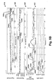
- FIGS. 5A-5B illustrate graphs showing operation of a disclosed FMCW radar system having a feedback path with signal correction element.
- Graphs 500 , 506 , 510 , and 514 illustrate the disclosed FMCW radar system operating on a reflected signal having no stored compensation parameters.
- Graphs 516 , 522 , 526 , and 532 illustrate the disclosed FMCW radar system operating on a reflected signal having stored compensation parameters.
- Graph 500 illustrates a signal strength of a reflected signal (y-axis) as a function of time (x-axis) for a measurement sweep of the reflected signal having a normalized time of 2 units.
- the reflected signal comprises four frequency channels 502 a - 502 d .
- the signal strength of each of the four frequency channels 502 a - 502 d has a high frequency component and low frequency and/or DC components.
- frequency channel 502 c has a low frequency component having a half period of approximately 1.4 units.
- Graph 500 further illustrates a correction signal 504 . Since no compensation parameters are stored for a ramped signal of the reflected signal 502 , the correction signal 504 has a constant value of zero.
- Graph 506 illustrates a signal strength of a reflected signal that has been adjusted according to the correction signal 504 (y-axis) as a function of time (x-axis). As shown in graph 506 , since the correction signal 504 has a constant value of zero, the signal strength of the adjusted signal in graph 508 a - 508 d is equal to the signal strength of the reflected signal in graph 500 .
- Graph 510 illustrates a signal strength of a reflected signal that has been adjusted according to the correction signal 504 (y-axis) as a function of frequency (x-axis). As shown in graph 510 , the reflected signal 512 a - 512 d has a high signal strength at low frequencies and at DC frequencies corresponding to unwanted signal components.
- Graph 514 illustrates a reduction in the signal level provided by the correction signal 504 (y-axis) as a function of frequency (x-axis). As shown in graph 514 , since the correction signal 504 has a constant value of zero, the signal level of the reflected signal is not adjusted at any frequency.
- Graph 516 illustrates a signal strength of a reflected signal (y-axis) as a function of time (x-axis) for a measurement sweep of the reflected signal.
- the reflected signal comprises four frequency channels 518 a - 518 d having a high frequency component and low frequency and/or DC components.
- Graph 516 further illustrates correction signals 520 a - 520 d for each of the four frequency channels. For example, a first correction signal 520 a is selected to reduce the unwanted low frequency signal of a reflected signal in the first frequency channel 518 a , a second correction signal 520 b is selected to reduce the unwanted low frequency signal of a reflected signal in the second frequency channel 518 b , etc. Since compensation parameters are stored for a ramped signal of reflected signal 518 , the correction signals 520 a - 520 d have a non-zero value.
- Graph 522 illustrates a signal strength of an adjusted signal that has been adjusted according to the correction signals 520 a - 520 d (y-axis) as a function of time (x-axis). Since the correction signals 520 a - 520 d have a non-zero value, they reduce the unwanted signal components, resulting in adjusted signals 524 a - 524 d for each of the four channels that have a signal strength less than that of the reflected signal in graph 516 .
- Graph 526 illustrates a signal strength of the adjusted signal (y-axis) as a function of frequency (x-axis).
- the signal level of the adjusted signal 530 a - 530 d is reduced at low frequencies and at DC frequencies relative to the unadjusted signals 528 a - 528 d , but is relatively unchanged at higher frequencies. Therefore, the correction signals 520 a - 520 d accurately reduce unwanted low frequency and DC signal components without altering higher frequency useful signal components.
- Graph 530 illustrates a reduction in the signal level provided by the correction signals 520 a - 520 d (y-axis) as a function of frequency (x-axis). As shown in graph 530 , the signal levels of the adjusted signals 530 a - 530 d are reduced by between approximately 20 to 30 dB for DC signals and for smaller amounts for low frequency signals. Furthermore, for higher frequencies, the signal levels of the adjusted signals 530 a - 530 d are not reduced.
- FIG. 6A is a block diagram of a disclosed FMCW radar system 600 having a feedback path comprising an analog polynomial generator 610 configured to generate a correction signal S cor that accounts for unwanted signal components in a reflected signal.
- the feedback path comprises an IF (intermediate frequency) parameter extraction element 602 .
- the IF parameter extraction element 602 is configured to time divide a received measurement sweep of a reflected signal into an equal number of sections, to sum the signal within the sections, and from the sums to generate one or more compensation parameters.
- the IF parameter extraction element 602 is configured to divide a received signal into four equal time-domain quarters. The IF parameter extraction element 602 then sums the signal within the quarters and from the sums calculates compensation parameters for a square law polynomial correction signal.
- the IF parameter extraction element 602 comprises an adder 604 connected to an accumulator 606 .
- a feedback path extends from the output of the accumulator 606 to an input of the adder 604 , such that the output of the accumulator 606 is added to a feedback signal S fb received by the adder 604 .
- the accumulator 606 sums the reflected signal to generate one or more partial sums Q n for a measurement sweep.
- the one or more partial sums Q n are provided to a compensation parameter calculation element 608 configured to calculate one or more compensation parameters from the partial sums Q n .
- the accumulator 606 is configured to receive a reset signal S reset from the transmit system controller 616 .
- the reset signal S reset resets the value of the accumulator 606 in a manner that splits the measurement sweep into a plurality of sections in the time-domain. By splitting the measurement sweep into a plurality of sections, a partial sum Q n is generated for each section.
- the reset signal comprises the trigger signal S trig .
- the IF parameter extraction element 602 is configured to generate first, second, and third compensation parameters (a, b, and c) for a second order polynomial correction signal.
- the IF parameter extraction element 602 splits a measurement sweep into four quarters.
- the accumulator 606 is configured to generate partial sums, Q 1 -Q 4 , for the four quarters of the measurement sweep.
- the IF parameter extraction element 602 is configured to write the one or more compensation parameters to a memory element 618 configured to store one or more compensation parameters corresponding to various ramped signals.
- the memory element 618 may be comprised within the transmit system controller 616 .
- the transmit system controller 616 is configured to provide the one or more compensation parameters corresponding to the ramped signal S ramp to an analog polynomial generator 612 by way of a digital-to-analog converter (DAC) 609 configured to convert the compensation parameters from a digital signal to an analog signal.
- the analog polynomial generator 612 is configured to generate an analog correction signal S cor comprising a polynomial function.
- the analog correction signal S cor may be filtered by a filtering element 614 before being provided to adder 216 , which subtracts the correction signal S cor from the mixed signal S mix to reduce unwanted signal components.
- FIG. 6B is a block diagram of some embodiments of an analog polynomial generator 620 configured to generate a second degree polynomial (e.g., at 2 +bt+c).
- an analog polynomial generator 620 configured to generate a second degree polynomial (e.g., at 2 +bt+c).
- the analog polynomial generator 620 comprises a first analog accumulator 622 , a first adder 624 , a second analog accumulator 626 , and a second adder 628 .
- the first accumulator 622 is configured to receive an initialization signal (e.g., trigger signal S trig ) and a first compensation parameter a. Upon receiving the initialization signal, the first accumulator 622 begins to integrate the value of a in time to generate a signal having a value of at.
- the first adder 624 is configured to add the output of the first accumulator 622 to a second compensation parameter b to generate a signal having a value of at +b.
- the second accumulator 626 is configured to receive the initialization signal and the signal having a value of at +b. Upon receiving the initialization signal, the second accumulator 626 begins to integrate the value of at +b in time to generate a signal having a value of at 2 +bt.
- the second adder 628 is configured to add the output of the second accumulator 626 to a third compensation parameter c to generate a correction signal S cor comprising a second order polynomial having a value of at 2 +bt+c.
- FIG. 7A is a block diagram of a disclosed FMCW radar system 700 having a feedback path comprising a digital polynomial generator 704 configured to generate a correction signal S cor that accounts for unwanted signal components in a reflected signal.
- the digital polynomial generator 704 is configured to receive one or more compensation parameters from a memory element 618 and from the one or more compensation parameters to generate a digital correction signal S cor comprising a polynomial function.
- the digital correction signal S cor is provided to a digital-to-analog converter 706 configured to convert to the digital correction signal S cor to an analog signal.
- the analog signal may be filtered by a filtering element 614 before being provided to adder 216 , which subtracts the correction signal S cor from the mixed signal S mix to reduce unwanted signal components.
- FIG. 7B is a block diagram of some embodiments of a digital polynomial generator 708 .
- the digital polynomial generator 708 comprises a first adder 710 , a first digital accumulator 712 , a second adder 714 , a third adder 716 , a second digital accumulator 718 , and a fourth adder 720 .
- the first adder 710 is configured to receive an initialization signal init (e.g., trigger signal S trig ) and a first input parameter p 2 .
- the first adder 710 has an output node connected to an input node of the first accumulator 712 .
- a feedback path extends from an output node of the first accumulator 712 to an input node of the first adder 710 , to generate a signal having a value of p 2 t.
- the second adder 714 is configured to add a second input parameter p 1 to the signal having a value of p 2 t to generate a signal having a value p 2 t+p 1 .
- the second adder 714 has an output node connected to an input node of a third adder 716 .
- the third adder 716 has an output node connected to an input node of the second accumulator 718 .
- a feedback path extends from an output node of the second accumulator 718 to an input node of the third adder 716 , to generate a signal having a value of 1 ⁇ 2p 2 t 2 ⁇ 1 ⁇ 2p 2 t+p 1 t.
- the fourth adder 720 has an input node connected to an output node of the second accumulator 718 and is configured to add a third input parameter p 0 to the signal having a value of 1 ⁇ 2p 2 t 2 ⁇ 1 ⁇ 2p 2 t+p 1 t, to generate an output signal having a value 1 ⁇ 2p 2 t 2 ⁇ 1 ⁇ 2p 2 t+p 1 t+p 0 .
- a parameter conversion element 722 is configured to receive the compensation parameters a, b, and c and to perform a substitution of coefficients according to a recurrence relation, as is well known to one of ordinary skill in the art.
- FIG. 8 is a flow diagram of an exemplary method 800 of reducing unwanted signal components (e.g., low frequency and DC signal components) in a FMCW radar system.
- unwanted signal components e.g., low frequency and DC signal components
- method 800 is illustrated and described below as a series of acts or events, the illustrated ordering of such acts or events are not to be interpreted in a limiting sense. For example, some acts may occur in different orders and/or concurrently with other acts or events apart from those illustrated and/or described herein. In addition, not all illustrated acts may be required to implement one or more aspects or embodiments of the disclosure herein. Also, one or more of the acts depicted herein may be carried out in one or more separate acts and/or phases.
- the reflected signal comprises a signal transmitted from a radar system, which has reflected off of an object and returned to the radar system.
- the reflected signal is mixed with a ramped signal having a continually varying frequency ramp.
- the ramped signal may comprise a sawtooth waveform.
- method 800 may check to determine if one or more compensation parameters corresponding to the ramped signal are stored in memory (e.g., from a prior measurement sweep) at 806 . In other embodiments, wherein the one or more compensation parameters have been pre-loaded into memory, acts 806 - 810 may be skipped.
- a correction signal may be selectively generated from one or more stored compensation parameters corresponding to the ramped signal, at 808 .
- the correction signal is subtracted from the mixed signal.
- the correction signal reduces unwanted frequency components (e.g., low frequency and/or DC components) in the mixed signal.
- the correction signal may comprise a polynomial function or harmonic functions.
- one or more compensation parameters corresponding to unwanted signal components are generated.
- the compensation parameters are generated by dividing a measurement sweep of the mixed signal (a temporal section of the mixed signal generated at 804 ) into a number of equal time-domain sections at 814 .
- signals in each of the equal time-domain sections are integrated to generate a number of partial sums equal to the number of equal time-domain sections.
- the partial sums are then mathematically operated upon to generate the one or more compensation parameters at 818 .
- one or more compensation parameters corresponding to the ramped signal are stored.
- the method may repeat over multiple measurement sweeps. After one or more compensation parameters are stored for a ramped signal ( 820 ), a correction signal corresponding to the ramped signal may be determined from one or more stored compensation parameters at 808 .
Abstract
Description
a=−Q 1 −Q 2 +Q 3 +Q 4,
b=2*(Q 1 −Q 2 −Q 3 +Q 4), and
c=⅙(−Q 1+7*Q 2+7*Q 3 −Q 4).
p 0 =c
p 1 =a+b
p 2=2*a
The input parameters p0, p1, and p2 are fed into the digital polynomial generator 508, so that the digital
Claims (21)
Priority Applications (3)
| Application Number | Priority Date | Filing Date | Title |
|---|---|---|---|
| US13/710,963 US9151827B2 (en) | 2012-12-11 | 2012-12-11 | Compensating slowly varying if DC offsets in receivers |
| CN201310668411.3A CN103869294B (en) | 2012-12-11 | 2013-12-11 | Compensate the slowly varying intermediate frequency DC skew in receiver |
| DE102013113859.4A DE102013113859A1 (en) | 2012-12-11 | 2013-12-11 | Compensating slowly varying intermediate frequency DC voltage offsets in receivers |
Applications Claiming Priority (1)
| Application Number | Priority Date | Filing Date | Title |
|---|---|---|---|
| US13/710,963 US9151827B2 (en) | 2012-12-11 | 2012-12-11 | Compensating slowly varying if DC offsets in receivers |
Publications (2)
| Publication Number | Publication Date |
|---|---|
| US20140159943A1 US20140159943A1 (en) | 2014-06-12 |
| US9151827B2 true US9151827B2 (en) | 2015-10-06 |
Family
ID=50778305
Family Applications (1)
| Application Number | Title | Priority Date | Filing Date |
|---|---|---|---|
| US13/710,963 Active 2033-12-31 US9151827B2 (en) | 2012-12-11 | 2012-12-11 | Compensating slowly varying if DC offsets in receivers |
Country Status (3)
| Country | Link |
|---|---|
| US (1) | US9151827B2 (en) |
| CN (1) | CN103869294B (en) |
| DE (1) | DE102013113859A1 (en) |
Cited By (3)
| Publication number | Priority date | Publication date | Assignee | Title |
|---|---|---|---|---|
| US20200348393A1 (en) * | 2014-12-23 | 2020-11-05 | Infineon Technologies Ag | System and Method for Radar |
| US20210141052A1 (en) * | 2019-11-08 | 2021-05-13 | Richwave Technology Corp. | Radar and Method of Updating Background Components of Echo Signal of Radar |
| US20210208266A1 (en) * | 2018-05-18 | 2021-07-08 | Polyvalor, Limited Partnershi | Fundamental-and-harmonics multi-frequency doppler radar system with radar motion cancellation |
Families Citing this family (7)
| Publication number | Priority date | Publication date | Assignee | Title |
|---|---|---|---|---|
| DE102010030628A1 (en) * | 2010-06-29 | 2011-12-29 | Robert Bosch Gmbh | Radar sensor for motor vehicles |
| US9151827B2 (en) * | 2012-12-11 | 2015-10-06 | Infineon Technologies Ag | Compensating slowly varying if DC offsets in receivers |
| KR101465370B1 (en) * | 2013-12-09 | 2014-11-26 | 한국항공우주연구원 | Apparatus and method of generating of direct digital synthesizer chirp signal using phase accumulation polynomial |
| KR20150134126A (en) * | 2014-05-21 | 2015-12-01 | 재단법인대구경북과학기술원 | Method and apparatus for processing radar signal |
| GB2544753B (en) * | 2015-11-24 | 2021-12-08 | Trw Ltd | Transceiver Circuits |
| KR102582054B1 (en) * | 2016-03-31 | 2023-09-25 | 한국전자통신연구원 | Pulse radar apparatus and method for operating pulse radar apparatus |
| US11237649B2 (en) * | 2017-08-10 | 2022-02-01 | Mediatek Singapore Pte. Ltd. | Inductive beacon for time-keying virtual reality applications |
Citations (14)
| Publication number | Priority date | Publication date | Assignee | Title |
|---|---|---|---|---|
| US4593287A (en) * | 1982-09-30 | 1986-06-03 | The Boeing Company | FM/CW sweep linearizer and method therefor |
| US5990738A (en) * | 1998-06-19 | 1999-11-23 | Datum Telegraphic Inc. | Compensation system and methods for a linear power amplifier |
| US6054896A (en) * | 1998-12-17 | 2000-04-25 | Datum Telegraphic Inc. | Controller and associated methods for a linc linear power amplifier |
| US6054894A (en) * | 1998-06-19 | 2000-04-25 | Datum Telegraphic Inc. | Digital control of a linc linear power amplifier |
| US20040041727A1 (en) * | 2002-08-30 | 2004-03-04 | Fujitsu Limited | Crossover detection method, radar apparatus and crossover detection program |
| US20080100500A1 (en) * | 2006-10-31 | 2008-05-01 | Hitachi, Ltd. | Radar, radio frequency sensor, and radar detection method |
| US7737885B2 (en) | 2007-08-01 | 2010-06-15 | Infineon Technologies Ag | Ramp linearization for FMCW radar using digital down-conversion of a sampled VCO signal |
| US7952501B2 (en) | 2007-05-11 | 2011-05-31 | Sung Wan Kim | Demodulator capable of compensating offset voltage of RF signal and method thereof |
| US8068804B2 (en) | 2008-12-29 | 2011-11-29 | Intel Corporation | Receiver local oscillator leakage compensation in the presence of an interferer |
| US8203481B2 (en) * | 2006-10-06 | 2012-06-19 | Adc Automotive Distance Control Systems Gmbh | Radar system for detecting the surroundings with compensation of interfering signals |
| US20130154703A1 (en) * | 2011-12-15 | 2013-06-20 | Intel Mobile Communications GmbH | Method and System to Measure and Compensate undue DCO Frequency Peaks at GFSK Ramp Down |
| US20140159943A1 (en) * | 2012-12-11 | 2014-06-12 | Infineon Technologies Ag | Compensating Slowly Varying IF DC Offsets in Receivers |
| US9020454B2 (en) * | 2006-02-15 | 2015-04-28 | Texas Instruments Incorporated | Linearization and calibration predistortion of a digitally controlled power amplifier |
| US9019154B2 (en) * | 2011-09-29 | 2015-04-28 | Infineon Technologies Ag | Radar circuit, radar system and method for testing |
Family Cites Families (5)
| Publication number | Priority date | Publication date | Assignee | Title |
|---|---|---|---|---|
| US4760319A (en) * | 1987-02-27 | 1988-07-26 | Magnetic Peripherals Inc. | Circuit for removing unwanted slope transitions from an incoming signal |
| US5068663A (en) * | 1991-01-24 | 1991-11-26 | Valentine Research, Inc. | Motor vehicle radar detector including amplitude detection |
| JP2000065930A (en) * | 1998-08-26 | 2000-03-03 | Nissan Motor Co Ltd | Radar apparatus for vehicle |
| US7450051B1 (en) * | 2005-11-18 | 2008-11-11 | Valentine Research, Inc. | Systems and methods for discriminating signals in a multi-band detector |
| DE102010030628A1 (en) * | 2010-06-29 | 2011-12-29 | Robert Bosch Gmbh | Radar sensor for motor vehicles |
-
2012
- 2012-12-11 US US13/710,963 patent/US9151827B2/en active Active
-
2013
- 2013-12-11 CN CN201310668411.3A patent/CN103869294B/en not_active Expired - Fee Related
- 2013-12-11 DE DE102013113859.4A patent/DE102013113859A1/en not_active Withdrawn
Patent Citations (14)
| Publication number | Priority date | Publication date | Assignee | Title |
|---|---|---|---|---|
| US4593287A (en) * | 1982-09-30 | 1986-06-03 | The Boeing Company | FM/CW sweep linearizer and method therefor |
| US5990738A (en) * | 1998-06-19 | 1999-11-23 | Datum Telegraphic Inc. | Compensation system and methods for a linear power amplifier |
| US6054894A (en) * | 1998-06-19 | 2000-04-25 | Datum Telegraphic Inc. | Digital control of a linc linear power amplifier |
| US6054896A (en) * | 1998-12-17 | 2000-04-25 | Datum Telegraphic Inc. | Controller and associated methods for a linc linear power amplifier |
| US20040041727A1 (en) * | 2002-08-30 | 2004-03-04 | Fujitsu Limited | Crossover detection method, radar apparatus and crossover detection program |
| US9020454B2 (en) * | 2006-02-15 | 2015-04-28 | Texas Instruments Incorporated | Linearization and calibration predistortion of a digitally controlled power amplifier |
| US8203481B2 (en) * | 2006-10-06 | 2012-06-19 | Adc Automotive Distance Control Systems Gmbh | Radar system for detecting the surroundings with compensation of interfering signals |
| US20080100500A1 (en) * | 2006-10-31 | 2008-05-01 | Hitachi, Ltd. | Radar, radio frequency sensor, and radar detection method |
| US7952501B2 (en) | 2007-05-11 | 2011-05-31 | Sung Wan Kim | Demodulator capable of compensating offset voltage of RF signal and method thereof |
| US7737885B2 (en) | 2007-08-01 | 2010-06-15 | Infineon Technologies Ag | Ramp linearization for FMCW radar using digital down-conversion of a sampled VCO signal |
| US8068804B2 (en) | 2008-12-29 | 2011-11-29 | Intel Corporation | Receiver local oscillator leakage compensation in the presence of an interferer |
| US9019154B2 (en) * | 2011-09-29 | 2015-04-28 | Infineon Technologies Ag | Radar circuit, radar system and method for testing |
| US20130154703A1 (en) * | 2011-12-15 | 2013-06-20 | Intel Mobile Communications GmbH | Method and System to Measure and Compensate undue DCO Frequency Peaks at GFSK Ramp Down |
| US20140159943A1 (en) * | 2012-12-11 | 2014-06-12 | Infineon Technologies Ag | Compensating Slowly Varying IF DC Offsets in Receivers |
Non-Patent Citations (1)
| Title |
|---|
| "Frequency-Modulated Continuous-Wave Radar"; Radar Basics http://www.radartutorial.eu/02.basics/rp07.en.html; Nov. 14, 2012, p. 1-2. |
Cited By (4)
| Publication number | Priority date | Publication date | Assignee | Title |
|---|---|---|---|---|
| US20200348393A1 (en) * | 2014-12-23 | 2020-11-05 | Infineon Technologies Ag | System and Method for Radar |
| US20210208266A1 (en) * | 2018-05-18 | 2021-07-08 | Polyvalor, Limited Partnershi | Fundamental-and-harmonics multi-frequency doppler radar system with radar motion cancellation |
| US20210141052A1 (en) * | 2019-11-08 | 2021-05-13 | Richwave Technology Corp. | Radar and Method of Updating Background Components of Echo Signal of Radar |
| US11573287B2 (en) * | 2019-11-08 | 2023-02-07 | Richwave Technology Corp. | Radar and method of updating background components of echo signal of radar |
Also Published As
| Publication number | Publication date |
|---|---|
| DE102013113859A1 (en) | 2014-06-12 |
| US20140159943A1 (en) | 2014-06-12 |
| CN103869294A (en) | 2014-06-18 |
| CN103869294B (en) | 2016-10-05 |
Similar Documents
| Publication | Publication Date | Title |
|---|---|---|
| US9151827B2 (en) | Compensating slowly varying if DC offsets in receivers | |
| US11650285B2 (en) | Chirp frequency non-linearity mitigation in radar systems | |
| CN107976656B (en) | Radar transceiver with phase noise cancellation | |
| US7737885B2 (en) | Ramp linearization for FMCW radar using digital down-conversion of a sampled VCO signal | |
| KR102197588B1 (en) | Integrated multi-channel rf circuit with phase sensing | |
| CA2744567C (en) | System employing a direct digital synthesiser | |
| US8823583B2 (en) | Radar sensor having two oscillators, two I/Q transmit mixers, and two I/Q receive mixers | |
| US10145937B2 (en) | Dynamic IQ mismatch correction in FMCW radar | |
| CN107250833B (en) | Radar apparatus | |
| US20180011181A1 (en) | Radar systems and methods thereof | |
| WO2016031108A1 (en) | Fmcw radar | |
| EP3260881B1 (en) | Fm-cw radar and fm-cw signal generation method | |
| US11029388B2 (en) | Spectral estimation of noise in radar apparatus | |
| US7982663B2 (en) | Digital signal processor | |
| WO2006040263A1 (en) | Electro-optical method for measuring distance and detecting a non-ideal chirp profile | |
| US10505770B2 (en) | Reception signal processing device, radar, and object detection method | |
| Dao et al. | A two sweeping VCO source for heterodyne FMCW radar | |
| CN112204421B (en) | Radar apparatus, control circuit, and program storage medium | |
| JP2011127923A (en) | Radar system | |
| KR20100009846A (en) | Method and apparatus for improving linearity of fmcw(frequency-modulated continuous wave) radar system | |
| Carlowitz et al. | A low power pulse frequency modulated UWB radar transmitter concept based on switched injection locked harmonic sampling |
Legal Events
| Date | Code | Title | Description |
|---|---|---|---|
| AS | Assignment |
Owner name: INFINEON TECHNOLOGIES AG, GERMANY Free format text: ASSIGNMENT OF ASSIGNORS INTEREST;ASSIGNOR:JAEGER, HERBERT, DR.;REEL/FRAME:029446/0176 Effective date: 20121211 |
|
| STCF | Information on status: patent grant |
Free format text: PATENTED CASE |
|
| MAFP | Maintenance fee payment |
Free format text: PAYMENT OF MAINTENANCE FEE, 4TH YEAR, LARGE ENTITY (ORIGINAL EVENT CODE: M1551); ENTITY STATUS OF PATENT OWNER: LARGE ENTITY Year of fee payment: 4 |
|
| MAFP | Maintenance fee payment |
Free format text: PAYMENT OF MAINTENANCE FEE, 8TH YEAR, LARGE ENTITY (ORIGINAL EVENT CODE: M1552); ENTITY STATUS OF PATENT OWNER: LARGE ENTITY Year of fee payment: 8 |