US9204849B2 - Radiation detection panel, radiation imaging device, and diagnostic imaging device - Google Patents

Radiation detection panel, radiation imaging device, and diagnostic imaging device Download PDF

Info

Publication number
US9204849B2
US9204849B2 US13/959,778 US201313959778A US9204849B2 US 9204849 B2 US9204849 B2 US 9204849B2 US 201313959778 A US201313959778 A US 201313959778A US 9204849 B2 US9204849 B2 US 9204849B2
Authority
US
United States
Prior art keywords
output circuit
transistor
signal
radiation
imaging device
Prior art date
Legal status (The legal status is an assumption and is not a legal conclusion. Google has not performed a legal analysis and makes no representation as to the accuracy of the status listed.)
Expired - Fee Related, expires
Application number
US13/959,778
Other versions
US20140056405A1 (en
Inventor
Yoshiyuki Kurokawa
Takayuki Ikeda
Current Assignee (The listed assignees may be inaccurate. Google has not performed a legal analysis and makes no representation or warranty as to the accuracy of the list.)
Semiconductor Energy Laboratory Co Ltd
Original Assignee
Semiconductor Energy Laboratory Co Ltd
Priority date (The priority date is an assumption and is not a legal conclusion. Google has not performed a legal analysis and makes no representation as to the accuracy of the date listed.)
Filing date
Publication date
Application filed by Semiconductor Energy Laboratory Co Ltd filed Critical Semiconductor Energy Laboratory Co Ltd
Assigned to SEMICONDUCTOR ENERGY LABORATORY CO., LTD. reassignment SEMICONDUCTOR ENERGY LABORATORY CO., LTD. ASSIGNMENT OF ASSIGNORS INTEREST (SEE DOCUMENT FOR DETAILS). Assignors: IKEDA, TAKAYUKI, KUROKAWA, YOSHIYUKI
Publication of US20140056405A1 publication Critical patent/US20140056405A1/en
Application granted granted Critical
Publication of US9204849B2 publication Critical patent/US9204849B2/en
Expired - Fee Related legal-status Critical Current
Adjusted expiration legal-status Critical

Links

Images

Classifications

    • GPHYSICS
    • G01MEASURING; TESTING
    • G01TMEASUREMENT OF NUCLEAR OR X-RADIATION
    • G01T1/00Measuring X-radiation, gamma radiation, corpuscular radiation, or cosmic radiation
    • G01T1/16Measuring radiation intensity
    • G01T1/20Measuring radiation intensity with scintillation detectors
    • AHUMAN NECESSITIES
    • A61MEDICAL OR VETERINARY SCIENCE; HYGIENE
    • A61BDIAGNOSIS; SURGERY; IDENTIFICATION
    • A61B6/00Apparatus for radiation diagnosis, e.g. combined with radiation therapy equipment
    • A61B6/42Apparatus for radiation diagnosis, e.g. combined with radiation therapy equipment with arrangements for detecting radiation specially adapted for radiation diagnosis
    • A61B6/4208Apparatus for radiation diagnosis, e.g. combined with radiation therapy equipment with arrangements for detecting radiation specially adapted for radiation diagnosis characterised by using a particular type of detector
    • GPHYSICS
    • G01MEASURING; TESTING
    • G01TMEASUREMENT OF NUCLEAR OR X-RADIATION
    • G01T1/00Measuring X-radiation, gamma radiation, corpuscular radiation, or cosmic radiation
    • G01T1/16Measuring radiation intensity
    • G01T1/20Measuring radiation intensity with scintillation detectors
    • G01T1/2018Scintillation-photodiode combinations
    • GPHYSICS
    • G01MEASURING; TESTING
    • G01TMEASUREMENT OF NUCLEAR OR X-RADIATION
    • G01T1/00Measuring X-radiation, gamma radiation, corpuscular radiation, or cosmic radiation
    • G01T1/16Measuring radiation intensity
    • G01T1/20Measuring radiation intensity with scintillation detectors
    • G01T1/208Circuits specially adapted for scintillation detectors, e.g. for the photo-multiplier section
    • HELECTRICITY
    • H04ELECTRIC COMMUNICATION TECHNIQUE
    • H04NPICTORIAL COMMUNICATION, e.g. TELEVISION
    • H04N25/00Circuitry of solid-state image sensors [SSIS]; Control thereof
    • H04N25/60Noise processing, e.g. detecting, correcting, reducing or removing noise
    • H04N25/63Noise processing, e.g. detecting, correcting, reducing or removing noise applied to dark current
    • HELECTRICITY
    • H04ELECTRIC COMMUNICATION TECHNIQUE
    • H04NPICTORIAL COMMUNICATION, e.g. TELEVISION
    • H04N25/00Circuitry of solid-state image sensors [SSIS]; Control thereof
    • H04N25/70SSIS architectures; Circuits associated therewith
    • H04N25/71Charge-coupled device [CCD] sensors; Charge-transfer registers specially adapted for CCD sensors
    • H04N25/75Circuitry for providing, modifying or processing image signals from the pixel array
    • HELECTRICITY
    • H04ELECTRIC COMMUNICATION TECHNIQUE
    • H04NPICTORIAL COMMUNICATION, e.g. TELEVISION
    • H04N5/00Details of television systems
    • H04N5/30Transforming light or analogous information into electric information
    • H04N5/32Transforming X-rays

Definitions

  • the present invention relates to a radiation detection panel and a radiation imaging device including the radiation detection panel.
  • the radiation imaging device particularly relates to a diagnostic imaging device in which a radiation source can emit X-rays.
  • a device that images an object with radiation (hereinafter referred to as a radiation imaging device) is used in various applications in medical and industrial fields; for example, in the medical field, a diagnostic imaging device that images the inside of a human body with X-rays is widely used in medical practice.
  • an X-ray source emits X-rays to a specific part (e.g., a bone or a lung) of a patient, and X-rays passing through the part are projected on a photographic film or the like. Then, the photographic film is developed, so that the inside of the specific part can be visualized.
  • a specific part e.g., a bone or a lung
  • An example of a method of digitizing imaging data is a method of using an imaging plate and a bio-imaging analyzer.
  • a plate (am imaging plate) in which a material layer that emits light when being irradiated with X-rays (such properties are referred to as stimulability or photostimulable properties) is formed on a support is used, and X-rays passing through a specific part of a patient are projected on the imaging plate.
  • X-ray projection light emitted from the plate is detected with a bio-imaging analyzer, whereby imaging data is constituted to obtain digitized data.
  • imaging data can be digitized by the method, the process is complicated because an image is first obtained as analog data by the imaging plate and then is digitized by the bio-imaging analyzer.
  • a radiation imaging device that obtains digital imaging data with the use of a radiation detection panel (also referred to as a flat panel detector) has recently received attention (e.g., see Patent Document 1).
  • the radiation detection panel is composed of a conversion unit that converts radiation (e.g., X-rays) emitted from a radiation source into charge or light (e.g., visible light), and a detection unit that includes a plurality of detection circuits for detecting the charge or the light.
  • Imaging data of an object can be digitized by being composed of signals output from the detection unit.
  • charge is generated directly from radiation, and a detection circuit generates an output signal with the use of the charge.
  • an indirect conversion flat panel detector radiation is first converted into light (e.g., a conversion unit generates visible light by being irradiated with X-rays), the light is further converted into charge, and a detection circuit generates an output signal with the use of the charge.
  • light e.g., a conversion unit generates visible light by being irradiated with X-rays
  • the light is further converted into charge
  • a detection circuit generates an output signal with the use of the charge.
  • Patent Document 1 Japanese Published Patent Application No. H11-316428
  • a signal constituting imaging data of the object (the signal is hereinafter referred to as a pixel signal) correctly represent the amount of radiation entering the conversion unit of the radiation detection panel (i.e., the amount of radiation passing through the object).
  • a conversion unit e.g., a scintillator of a radiation detection panel with indirect conversion
  • a phenomenon in which light emission continues even after radiation emission stops which is called afterglow.
  • afterglow a phenomenon in which light emission continues even after radiation emission stops
  • an interval long enough to sufficiently reduce afterglow is provided between stop of radiation emission (A 1 in FIG. 11A ) and the next radiation emission (A 2 in FIG. 11A ) as shown in FIG. 11A
  • adverse effect of afterglow on a signal output from a detection circuit can be reduced.
  • the next X-ray irradiation starts while a signal due to afterglow in the conversion unit is output from the detection circuit. Accordingly, as shown in FIG. 11B , a signal resulting from addition of signals due to the previous and earlier afterglows (corresponding to a region 1101 in FIG. 11B ) to a signal based on radiation emission (corresponding to a region 1100 in FIG. 11B ) is output from the detection circuit and serves as a pixel signal.
  • an object of one embodiment of the invention disclosed herein is to provide a radiation detection panel that outputs signals for generating an accurate pixel signal regardless of the performance of a conversion unit.
  • Another object of one embodiment of the invention disclosed herein is to provide a radiation imaging device that includes the radiation detection panel with the above characteristics and has high resolution to obtain a high-definition image.
  • a pixel signal should not include a signal due to afterglow.
  • a detection circuit that outputs signals used for generating one pixel signal is composed of a first output circuit that outputs a first signal including information on light emission due to afterglow, and a second output circuit that outputs a second signal including both information on light emission based on radiation emission and information on light emission due to afterglow.
  • the first output circuit detects the amount of light incident from a conversion unit in a period M (the amount corresponds to a region 1200 in FIG. 12 ). This amount of the incident light is due to afterglow in the conversion unit.
  • the second output circuit detects the amount of light incident from the conversion unit in a period N (the amount corresponds to a region 1201 in FIG. 12 ).
  • This incident light includes light from the conversion unit based on radiation emission and light from the conversion unit due to afterglow.
  • the period M and the period N are the same in length in FIG. 12 .
  • the light from the conversion unit due to afterglow is drastically decreased in a time as short as several milliseconds after the end of radiation emission, and then gradually decreased.
  • the amount of incident light due to afterglow in the period M and that in the period N become closer as the period M and the period N become shorter.
  • the first output circuit outputs a signal based on the amount of light incident from the conversion unit in the period M (hereinafter, the signal output from the first output circuit is called “first signal”)
  • the second output circuit outputs a signal based on the amount of light incident from the conversion unit in the period N (hereinafter, the signal output from the second output circuit is called “second signal”). Accordingly, a pixel signal can be produced using a difference between both these signals and as a result, accurate imaging data of an object can be obtained.
  • the detection unit detection of the amount of light incident from the conversion unit in the period M by the first output circuit and detection of the amount of light incident from the conversion unit in the period N by the second output circuit are sequentially performed in all detection circuits, and then the first signal and the second signal are output from each of the detection circuits. Accordingly, the first output circuit and the second output circuit included in each detection circuit need to hold data (which can also be represented as charge or potential) generated based on the amount of light incident from the conversion unit, at least until all the detection circuits complete the detection process.
  • each of the first and second output circuits is configured to hold the data between a drain (or a source) of a transistor using an oxide semiconductor material for a channel formation region and a gate of another transistor.
  • the bandgap of a film using an oxide semiconductor material is greater than or equal to 3.0 eV (electron volts), which is much wider than the bandgap of silicon (1.1 eV).
  • the off-resistance of a transistor is inversely proportional to the concentration of carriers thermally excited in a channel formation region. Since the bandgap of silicon is 1.1 eV even in a state where there is no carrier caused by a donor or an acceptor (i.e., even in the case of an intrinsic semiconductor), the concentration of thermally excited carriers at room temperature (200 K) is approximately 1 ⁇ 10 11 cm ⁇ 3 .
  • the bandgap of a film using an oxide semiconductor material is generally as wide as 3.0 eV or more as described above, and the concentration of thermally excited carriers in a film with a bandgap of 3.2 eV, for example, is approximately 1 ⁇ 10 ⁇ 7 cm ⁇ 3 .
  • the resistivity is inversely proportional to the carrier concentration, and thus the resistivity of the semiconductor with a bandgap of 3.2 eV is 18 orders of magnitude higher than that of silicon.
  • a transistor that uses such a wide bandgap oxide semiconductor material for a channel formation region can achieve extremely low off-state current, using the transistor in the above manner enables data generated based on the amount of light incident from the conversion unit to be held in the first output circuit and the second output circuit for a long time.
  • the first output circuit and the second output circuit can hold data based on the amount of light incident from the conversion unit (hereinafter the data in the first output circuit is referred to as first data and the data in the second output circuit is referred to as second data) until all the detection circuits complete the detection process.
  • each of the detection circuits outputs a signal generated using the first data (hereinafter the signal is referred to as the first signal) and a signal generated using the second data (hereinafter the signal is referred to as the second signal).
  • One embodiment of the present invention is a radiation detection panel including a conversion unit configured to convert radiation into light, and a detection unit including a plurality of detection circuits each having a first output circuit and a second output circuit.
  • the first output circuit and the second output circuit each include a photoelectric conversion element generating charge in response to light incident from the conversion unit, a first transistor in which a gate potential varies in accordance with the amount of the charge, a second transistor controlling a signal output from the first transistor, and a third transistor that holds the gate potential of the first transistor and uses an oxide semiconductor material for a channel formation region.
  • the first output circuit generates first data corresponding to the amount of charge generated by the photoelectric conversion element when radiation is not emitted, and holds the first data.
  • the second output circuit generates second data corresponding to the amount of charge generated by the photoelectric conversion element when radiation is emitted, and holds the second data.
  • the detection unit outputs a first signal generated using the first data and a second signal generated using the second data from each of the detection circuits after the first data is held in all the first output circuits and the second data is held in all the second output circuits in the detection unit.
  • the radiation detection panel having the above structure a signal component due to afterglow in the conversion unit can be eliminated, resulting in achievement of a radiation detection panel in which signals for generating an accurate pixel signal is obtained regardless of the performance of the conversion unit.
  • One of electrodes of the photoelectric conversion element is electrically connected to a first wiring, and the other is electrically connected to one of a source and a drain of the third transistor.
  • One of a source and a drain of the first transistor is electrically connected to a second wiring, and the other is electrically connected to one of a source and a drain of the second transistor.
  • the other of the source and the drain of the second transistor is electrically connected to a third wiring.
  • a gate of the second transistor is electrically connected to a fourth wiring.
  • the other of the source and the drain of the third transistor is electrically connected to a gate of the first transistor.
  • a gate of the third transistor is electrically connected to a fifth wiring.
  • the first output circuit and the second output circuit used for generating one pixel signal be provided adjacent to each other, because an accurate pixel signal is difficult to obtain when they are placed apart from each other.
  • the length of a time for the first output circuit to detect light (hereinafter also referred to as a first detection time) is preferably smaller than or equal to the length of a time for the second output circuit to detect light (hereinafter also referred to as a second detection time).
  • the amount of light due to afterglow is approximately the same in the first detection time and the second detection time; however, the amount of light due to afterglow in the second detection time is sometimes smaller than that in the first detection time depending on the material used for the conversion unit. Consequently, making the first detection period shorter than the second detection period can adjust a reduction in the amount of light due to afterglow in the second detection period.
  • At least one of the first transistor and the second transistor provided in each of the first and second output circuits may include a channel formation region formed using an oxide semiconductor material.
  • a radiation imaging device capable of obtaining accurate imaging data can be achieved by a combination of the radiation detection panel, a radiation source, and a pixel signal generation unit that generates a pixel signal by using a difference between the first signal and the second signal output from the radiation detection panel.
  • the radiation imaging device is a diagnostic imaging device in which the radiation source is an X-ray radiation source and the conversion unit includes a scintillator converting X-rays into visible light.
  • the diagnostic imaging device can diagnose an internal condition more correctly with a more accurate pixel signal and higher contrast.
  • the internal condition can be diagnosed correctly by obtainment of more segmented scan images by shortening each emission time for the radiation source and shortening an interval between detection operations, for example.
  • the detection circuit used for generating a pixel signal is composed of the first output circuit that outputs the first signal including information on light emission due to afterglow, and the second output circuit that outputs the second signal including both information on light emission based on radiation emission and information on light emission due to afterglow.
  • a transistor using an oxide semiconductor material for a channel formation region is used as some of the transistors included in the first and second output circuits.
  • the signal (the first signal or the second signal) can be held in each of the output circuits; therefore, after all the output circuits hold the signal (the first signal or the second signal), the first signal and the second signal can be sequentially output from the detection circuits.
  • pixel signals composing imaging data are produced using the first signals and the second signals that are output from the detection circuits included in the radiation detection panel.
  • the radiation imaging device can obtain accurate imaging data.
  • FIG. 1 illustrates the structure of a radiation detection panel
  • FIGS. 2A to 2E each illustrate the structure of a detection unit included in a radiation detection panel
  • FIG. 3A illustrates the structure of a detection circuit
  • FIG. 3B is a chart showing the operation of the detection circuit
  • FIG. 4 illustrates the structure of a detection unit
  • FIG. 5 is a chart showing the operation of a detection unit
  • FIGS. 6A to 6C each illustrate the structure of an operational amplifier circuit
  • FIG. 7A illustrates the structure of a detection unit different from that in Embodiment 1, and FIG. 7B is a chart showing the operation of the detection unit;
  • FIG. 8 illustrates the structure of a detection unit different from that in Embodiment 1;
  • FIG. 9A illustrates the structure of a detection unit different from that in Embodiment 1, and FIG. 9B is a chart showing the operation of the detection unit;
  • FIG. 10 illustrates the structure of a detection unit different from that in Embodiment 1;
  • FIGS. 11A and 11B each illustrate signals output from a detection circuit
  • FIG. 12 explains the concept of generating a pixel signal
  • FIG. 13 illustrates the structure of a radiation imaging device
  • FIGS. 14A and 14B illustrate the layout of a detection circuit
  • FIGS. 15A and 15B explain the concept of a method for obtaining a difference between detection signals.
  • one terminal of a transistor refers to one of a source electrode and a drain electrode
  • the other terminal of the transistor refers to the other of the source electrode and the drain electrode. That is, when one terminal of the transistor is the source electrode, the other terminal of the transistor refers to the drain electrode.
  • Embodiment 1 the structure of a radiation detection panel will be described with reference to FIG. 1 and FIGS. 2A to 2E .
  • a radiation detection panel 100 includes a conversion unit 101 that receives radiation 104 emitted from the outside and converts the radiation 104 into light, and a plurality of detection circuits 110 each including a first output circuit 111 and a second output circuit 112 each of which outputs a signal based on light 105 emitted from the conversion unit 101 .
  • the radiation 104 is emitted from a radiation source 103 and enters the radiation detection panel 100 .
  • An object 106 is disposed between the radiation detection panel 100 and the radiation source 103 .
  • the conversion unit 101 includes a substance that absorbs energy of incident radiation (e.g., X-rays, ⁇ -rays, ⁇ -rays, or neutron rays) and emits light (e.g., infrared rays, visible light, or ultraviolet rays) or a material containing the substance; known examples of such a substance and such a material are a material such as Gd 2 O 2 S:Tb, Gd 2 O 2 S:Pr, Gd 2 O 2 S:Eu, BaFCl:Eu, CsI:Ti, ZnS:Ag, LiF:W, or LiI:Eu, and a resin or ceramics in which any of the above materials is dispersed. Note that the substance after the colon represents an impurity mixed to facilitate the capture of excited electrons.
  • incident radiation e.g., X-rays, ⁇ -rays, ⁇ -rays, or neutron rays
  • light e.g., infrared rays
  • a detection unit 102 includes the plurality of detection circuits 110 each including the first output circuit 111 and the second output circuit 112 .
  • a pixel signal is generated using a first signal output from the first output circuit 111 and a second signal output from the second output circuit 112 in the detection circuit 110 .
  • the first output circuit and the second output circuit used for generating one pixel signal are placed apart from each other, an accurate pixel signal cannot be obtained in some cases.
  • a pixel signal is preferably generated using a pair of the first output circuit 111 and the second output circuit 112 that can receive light emitted from the conversion unit 101 under substantially the same conditions (i.e., that are provided at positions at which lights emitted from one point of the conversion unit 101 have approximately the same intensity). Consequently, the first output circuit 111 and the second output circuit 112 used in a pair to produce a pixel signal are preferably provided adjacent to each other.
  • the detection unit 102 seen from the above can have a structure in which a plurality of detection circuits 110 each have a pair of the first output circuit 111 and the second output circuit 112 adjacent in the horizontal direction as illustrated in FIG. 2A , a structure in which a plurality of detection circuits 110 each have a pair of the first output circuit 111 and the second output circuit 112 adjacent in the vertical direction as illustrated in FIG. 2B , or a structure in which a plurality of detection circuits 110 each have a pair of the first output circuit 111 and the second output circuit 112 adjacent in an oblique direction as illustrated in FIG. 2C .
  • first output circuits 111 and the second output circuits 112 are not necessarily arranged neatly in a matrix, and for example, as illustrated in FIG. 2D , a plurality of detection circuits 110 each having a pair of the first output circuit 111 and the second output circuit 112 may be misaligned (i.e., one pair of the first output circuit 111 and the second output circuit 112 may not be aligned with another pair).
  • a plurality of detection circuits 110 each having a pair of the first output circuit 111 and the second output circuit 112 may cross each other (i.e., in such a manner that one pair of the first output circuit 111 and the second output circuit 112 crosses another pair).
  • the first output circuit 111 and the second output circuit 112 may be placed in an inverted position.
  • the first output circuit 111 is placed on the left side of the detection circuit 110 and the second output circuit 112 is placed on the right side of the detection circuit 110 ; however, the first output circuit 111 may be placed on the right side of the detection circuit 110 and the second output circuit 112 may be placed on the left side of the detection circuit 110 .
  • first output circuit 111 and the second output circuit 112 An example of the configuration of the first output circuit 111 and the second output circuit 112 will be described below with reference to FIG. 3A . Note that the first output circuit 111 and the second output circuit 112 can have the same configuration.
  • the first output circuit 111 and the second output circuit 112 are configured to include a photoelectric conversion element 300 that generates charge in response to light emitted from the conversion unit 101 , a first transistor 301 in which a potential applied to a gate varies in accordance with the amount of charge generated by the photoelectric conversion element 300 , a second transistor 302 that controls a signal output from the first transistor 301 , and a third transistor 303 that holds the potential applied to the gate of the first transistor 301 (also referred to as the potential of a second wiring 312 ).
  • One electrode of the photoelectric conversion element 300 is connected to a first wiring 311 (also referred to as a wiring PR).
  • the gate of the first transistor 301 is electrically connected to the second wiring 312 (also referred to as a wiring FD).
  • One of a source and a drain of the first transistor 301 is electrically connected to a third wiring 313 (also referred to as a wiring VR).
  • the other of the source and the drain of the first transistor 301 is electrically connected to one of a source and a drain of the second transistor 302 .
  • the other of the source and the drain of the second transistor 302 is electrically connected to a fourth wiring 314 (also referred to as a wiring OUT).
  • a gate of the second transistor 302 is electrically connected to a fifth wiring 315 (also referred to as a wiring SE).
  • an integrator circuit may be connected to the fourth wiring 314 (OUT). Connecting the integrator circuit to the fourth wiring 314 (OUT) increases S/N, enabling detection of weaker light.
  • a specific configuration example of the integrator circuit will be described in Embodiment 2.
  • One of a source and a drain of the third transistor 303 provided between the photoelectric conversion element 300 and the first transistor 301 is electrically connected to the other electrode of the photoelectric conversion element 300 .
  • the other of the source and the drain of the third transistor 303 is electrically connected to the second wiring 312 (FD).
  • a gate of the third transistor 303 is electrically connected to a sixth wiring 316 (also referred to as a wiring TX).
  • Examples of the photoelectric conversion element 300 are an element that generates charge by receiving infrared rays, an element that generates charge by receiving visible light, and an element that generates charge by receiving ultraviolet rays.
  • the third transistor 303 in an off state needs to have a function of holding charge generated when the photoelectric conversion element 300 receives light, as a potential at the second wiring 312 ; consequently, the third transistor 303 needs to be a transistor with high mobility and extremely low off-state current. For this reason, an oxide semiconductor material is used for a channel formation region of the third transistor 303 .
  • FIG. 3A for easy understanding, “OS” is written beside the transistor using an oxide semiconductor material for a channel formation region.
  • the first transistor 301 can be a thin film transistor in which amorphous silicon, microcrystalline silicon, polycrystalline silicon, single crystal silicon, or the like is used for a channel formation region. Since the first transistor 301 is provided to amplify an electric signal generated by the photoelectric conversion element 300 , the first transistor 301 needs high mobility. Moreover, the first transistor 301 needs low off-state current in order to prevent output of an unnecessary potential to the third wiring 313 (VR). For these reasons, it is also effective to use a transistor that uses an oxide semiconductor material achieving both high mobility and low off-state current in a channel formation region.
  • the second transistor 302 can be a thin film transistor in which amorphous silicon, microcrystalline silicon, polycrystalline silicon, single crystal silicon, or the like is used for a channel formation region. Since the second transistor 302 is provided to control an output from the detection circuit 110 , the second transistor 302 needs high mobility. Further, the second transistor 302 needs low off-state current in order to prevent output of an unnecessary potential to the fourth wiring 314 (OUT). For these reasons, it is also effective to use a transistor that uses an oxide semiconductor material achieving both high mobility and low off-state current in a channel formation region.
  • transistors using an oxide semiconductor material for a channel formation region as all the transistors included in the detection circuit 110 can simplify the process of fabricating the detection circuit.
  • Connecting a capacitor to the fourth wiring 314 (OUT) is effective in stabilizing the potential of the fourth wiring 314 (OUT).
  • the first transistor 301 and the second transistor 302 are electrically connected in series in this order between the third wiring 313 (VR) and the fourth wiring 314 (OUT); alternatively, the first transistor 301 and the second transistor 302 may be connected in reverse. That is, the second transistor 302 and the first transistor 301 may be electrically connected in series in this order between the third wiring 313 (VR) and the fourth wiring 314 (OUT).
  • the third transistor 303 has a gate only on one side of a semiconductor layer; however, the third transistor 303 may have a pair of gates placed so that the semiconductor layer is sandwiched therebetween.
  • the third transistor 303 has a pair of gates placed so that the semiconductor layer is sandwiched therebetween, one of the gates can function as a front gate to which the potential of the second wiring 312 is applied, and the other gate can function as a backgate that controls the threshold voltage or the like of the third transistor 303 .
  • the potential applied to the other gate preferably ranges from ⁇ 20 V to +2 V with reference to the source potential. If a change in the threshold voltage of the third transistor 303 does not adversely affect the operation of the detection circuit 110 when the potential applied to the other gate varies in the above range, the other gate may be electrically isolated (floating).
  • the operation of the output circuit illustrated in FIG. 3A will be described with reference to a timing chart in FIG. 3B . Note that the first output circuit 111 and the second output circuit 112 can perform a read operation in the same manner.
  • signals 311 S, 312 S, 314 S, 315 S, and 316 S correspond to potentials of the first wiring 311 (PR), the second wiring 312 (FD), the fourth wiring 314 (OUT), the fifth wiring 315 (SE), and the sixth wiring 316 (TX) in FIG. 3A .
  • the potential of the third wiring 313 (VR) is fixed at low level.
  • the potential of the first wiring 311 (PR) (the signal 311 S) is set high and the potential of the sixth wiring 316 (TX) (the signal 316 S) is set high (i.e., a reset operation starts), so that a forward bias is applied to the photoelectric conversion element 300 and the potential of the second wiring 312 (FD) (the signal 312 S) becomes high.
  • the potential of the fourth wiring 314 (OUT) (the signal 314 S) is precharged to high level.
  • the potential of the first wiring 311 (PR) (the signal 311 S) is set low and the potential of the sixth wiring 316 (TX) (the signal 316 S) is kept high (i.e., the reset operation finishes and an accumulation operation starts), so that a photocurrent flows through the photoelectric conversion element 300 in response to light emitted from the conversion unit 101 , and the potential of the second wiring 312 (FD) (the signal 312 S) starts to be lowered.
  • the speed of decrease in the potential of the second wiring 312 (FD) (the signal 312 S) changes in accordance with the amount of emitted light.
  • the channel resistance between the source and the drain of the first transistor 301 changes in accordance with the amount of light emitted to the photoelectric conversion element 300 from the conversion unit 101 .
  • the potential of the sixth wiring 316 (TX) (the signal 316 S) is set low (i.e., the accumulation operation finishes).
  • the third transistor 303 is a transistor whose channel formation region is formed using an oxide semiconductor material as described above and thus has extremely low off-state current, the charge can be held at the second wiring 312 (FD), which is also referred to as the wiring between the other of the source and the drain of the third transistor and the gate of the first transistor, until a subsequent selection operation is performed.
  • the amount of the charge corresponds to data held in the output circuit (first data in the first output circuit 111 and second data in the second output circuit 112 ).
  • the potential of the second wiring 312 (FD) depends on the amount of charge generated by the photoelectric conversion element 300 during the accumulation operation. That is, the potential of the second wiring 312 (FD) changes in accordance with the amount of light emitted to the photoelectric conversion element 300 from the conversion unit 101 .
  • the potential of the sixth wiring 316 (TX) (the signal 316 S) is set low
  • the potential of the second wiring 312 (FD) sometimes changes because of parasitic capacitance between the sixth wiring 316 (TX) and the second wiring 312 (FD).
  • a large amount of potential change makes it impossible to obtain an accurate amount of charge generated by the photoelectric conversion element 300 during the accumulation operation.
  • Examples of effective measures to reduce the amount of potential change include reducing the capacitance between the gate and the source (or between the gate and the drain) of the third transistor 303 , increasing the gate capacitance of the first transistor 301 , and providing a storage capacitor to connect the second wiring 312 (FD). Note that in FIG. 3B , the potential change can be ignored by the adoption of these measures.
  • the potential of the fifth wiring 315 (SE) (the signal 315 S) is set high (i.e., the selection operation starts), so that the potential of the fourth wiring 314 (OUT) (the signal 314 S) decreases. Note that precharge of the fourth wiring 314 (OUT) is terminated before the time T 4 .
  • the speed of decrease in the potential of the fourth wiring 314 (OUT) depends on the channel resistance between the source and the drain of the first transistor 301 . That is, this speed changes in accordance with the amount of light emitted to the photoelectric conversion element 300 from the conversion unit 101 during the accumulation operation.
  • the potential of the fifth wiring 315 (SE) (the signal 315 S) is set low (i.e., the selection operation finishes), so that a current flowing between the source and the drain of the second transistor 302 is interrupted and the potential of the fourth wiring 314 (OUT) (the signal 314 S) becomes constant.
  • This potential corresponds to a signal output from the output circuit (the first signal in the first output circuit 111 and the second signal in the second output circuit 112 ).
  • the constant potential of the fourth wiring 314 (OUT) varies depending on the amount of light entering the photoelectric conversion element 300 from the conversion unit 101 .
  • the potential of the fourth wiring 314 (OUT) the signal 314 S
  • the amount of light entering the photoelectric conversion element 300 from the conversion unit 101 during the accumulation operation can be found.
  • the potential of the second wiring 312 (FD) (the signal 312 S) becomes lower and the gate potential of the first transistor 301 becomes lower; thus, the speed of decrease in the potential of the fourth wiring 314 (OUT) (the signal 314 S) becomes lower. As a result, the potential of the fourth wiring 314 (OUT) (the signal 314 S) is higher.
  • the potential of the second wiring 312 (FD) (the signal 312 S) becomes higher and the gate potential of the first transistor 301 becomes higher; thus, the speed of decrease in the potential of the fourth wiring 314 (OUT) (the signal 314 S) becomes higher. As a result, the potential of the fourth wiring 314 (OUT) (the signal 314 S) is lower.
  • the operation of the first output circuit 111 and the second output circuit 112 is performed by repetition of a sequence of the reset operation, the accumulation operation, and the selection operation.
  • first output circuit 111 and the second output circuit 112 are not limited to those illustrated in FIGS. 3A and 3B .
  • a different configuration of the first output circuit 111 and the second output circuit 112 and the operation flow for the configuration will be described in Embodiment 3.
  • the detection unit 102 includes the first output circuits 111 and the second output circuits 112 arranged in a matrix of m rows and n columns
  • the first output circuits 111 are provided in odd-numbered rows and the second output circuits 112 are provided in even-numbered rows. That is, the plurality of detection circuits 110 have the structure illustrated in FIG. 2B , in which the first output circuit and the second output circuit used for producing a pixel signal are arranged in the vertical direction.
  • FIG. 5 is an example of a timing chart showing the operation flow of the entire detection unit 102 and shows the operation of the area surrounded by dashed-dotted lines in FIG. 4 . Note that the operation of the first output circuit 111 and the second output circuit 112 is the same as that described above.
  • a signal PR( 1 ), a signal PR( 2 ), a signal PR( 3 ), and a signal PR( 4 ) correspond to the potentials of the wirings PR in the first row, the second row, the third row, and the fourth row, respectively, of pixels.
  • a signal TX( 1 ), a signal TX( 2 ), a signal TX( 3 ), and a signal TX( 4 ) correspond to the potentials of the wirings TX in the first row, the second row, the third row, and the fourth row, respectively, of the pixels.
  • a signal SE( 1 ), a signal SE( 2 ), a signal SE( 3 ), and a signal SE( 4 ) correspond to the potentials of the wirings SE in the first row, the second row, the third row, and the fourth row, respectively, of the pixels.
  • a period T fr is a period necessary for one imaging.
  • a period T re1 is a period during which the first output circuits 111 , which are the circuits in the first and third rows, perform the reset operation.
  • a period T ac1 is a period during which the first output circuits 111 perform the accumulation operation.
  • a period T re2 is a period during which the second output circuits 112 , which are the circuits in the second and fourth rows, perform the reset operation.
  • a period T ac2 is a period during which the second output circuits 112 perform the accumulation operation.
  • Periods T se1 to T se4 are periods during which the circuit in the first row (the first output circuit 111 ) to the circuit in the fourth row (the second output circuit 112 ) perform the selection operation.
  • the circuits in the first and third rows concurrently perform the reset operation or the accumulation operation
  • the circuits in the second and fourth rows concurrently perform the reset operation or the accumulation operation.
  • pixels in adjacent rows that is, in the first and second rows, the second and third rows, and the third and fourth rows perform the reset operation or the accumulation operation in different periods. After the accumulation operation is finished, the selection operation is sequentially performed from the first row.
  • the accumulation period of the circuits in the first and third rows (the first output circuits 111 ), that is, the period T ac1 is a period during which radiation is not emitted from the radiation source 103
  • the accumulation period of the circuits in the second and fourth rows (the second output circuits 112 ) is a period during which radiation is emitted from the radiation source 103 .
  • data (first data) corresponding to light emitted from the conversion unit 101 due to afterglow is generated in the first output circuit 111 in the period T ac1
  • data (second data) corresponding to light emitted from the conversion unit 101 due to radiation emission is generated in the second output circuit 112 in the period T ac2 .
  • the generated data are held in the respective circuits.
  • each output circuit in the detection unit 102 is sufficiently small in size
  • light detected by the detection circuit in the first row (the first output circuit 111 ) and light detected by the detection circuit in the second row (the second output circuit 112 ) can be considered as light emitted from the same point, that is, light generated in response to radiation emitted to the same point of the object.
  • light detected by the detection circuit in the third row (the first output circuit 111 ) and light detected by the detection circuit in the fourth row (the second output circuit 112 ) can be considered as light emitted from the same point, that is, light generated in response to radiation emitted to the same point of the object.
  • the amount of light due to afterglow is drastically decreased in about several milliseconds after the end of radiation emission, and then gradually decreased in general; therefore, the amount of light due to afterglow corresponding to radiation emitted before the period T ac2 can be considered to be approximately the same in the period T ac1 and the period T ac2 .
  • the radiation detection panel 100 can output signals for generating an accurate pixel signal regardless of the performance of the conversion unit 101 .
  • a system (hereinafter referred to as a pixel signal generation unit) that generates a pixel signal with the use of a difference between a first detection signal (the first signal) and a second detection signal (the second signal) may be provided in the radiation detection panel 100 , for example, in the detection unit 102 .
  • a pixel signal generation unit 1301 may be provided in a radiation imaging device 1300 together with the radiation source 103 and the radiation detection panel 100 and electrically connected to the radiation detection panel 100 .
  • an external output terminal 1302 electrically connected to the pixel signal generation unit 1301 is connected to a display device, and imaging data of the object is displayed.
  • the display device may be provided in the radiation imaging device 1300 .
  • the structure of the pixel signal generation unit 1301 can be determined as appropriate by a practitioner.
  • the amount of change in afterglow component between the period T ac1 and the period T ac2 becomes smaller and as a result, the amount of afterglow component in the period T ac1 and that in the period T ac2 can be made closer to each other.
  • a pixel signal generated using the first signal and the second signal can constitute a more accurate image.
  • the period T ac1 is preferably shorter than the period T ac2 .
  • the amount of light due to afterglow is approximately the same in the period T ac1 and the period T ac2 ; however, the amount of light due to afterglow in the period T ac2 is sometimes smaller than that in the period T ac1 depending on the material used for the conversion unit 101 . Consequently, making the period T ac1 shorter than the period T ac2 can adjust a reduction in the amount of light due to afterglow in the period T ac2 .
  • the amount of light due to afterglow in the period T ac1 and that in the period T ac2 can be made closer to each other in the following manner: after the first signal is obtained in the period T ac1 shortened as above, the second signal is obtained in the period T ac2 , and then a pixel signal is generated using a difference between the second signal and a signal obtained by integral multiple of the first signal.
  • the multiplier is not limited to ten.
  • the practitioner can determine, as appropriate in view of the properties of the material used for the conversion unit 101 or the like, how long the period T ac1 is relative to the period T ac2 ; how short the period T ac1 is compared to the period T ac2 ; whether the period T ac1 is multiplied; and how many times the period T ac1 is multiplied (what is the number to multiply the period T ac1 ), for example.
  • This embodiment shows the example where the accumulation periods of the output circuits are the same in the first and third rows and in the second and fourth rows; however, the structure is not limited to this as long as the accumulation periods are different between adjacent rows.
  • the accumulation periods of the output circuits are the same in the first and fourth rows and in the second and third rows so that radiation emission is stopped in the accumulation period in the first and fourth rows and radiation is emitted in the accumulation period in the second and third rows.
  • obtaining a difference between the adjacent first and second rows and between the adjacent third and fourth rows can provide similar effects to the above.
  • the radiation detection panel can output signals for generating an accurate pixel signal regardless of the performance of the conversion unit.
  • the radiation detection panel can be employed for a non-destructive imaging device using a radiation source emitting X-rays, ⁇ -rays, ⁇ -rays, or neutron rays.
  • the radiation detection panel can be used as a detection unit in a diagnostic imaging device in which a radiation source is an X-ray radiation source and a scintillator that converts X-rays into visible light is used for a conversion unit.
  • imaging devices using the radiation detection panel described in this embodiment can be high-performance devices capable of obtaining high-contrast images.
  • Embodiment 2 shows examples of the structure of an integrator circuit used to be connected to the fourth wiring 314 (OUT).
  • FIG. 6A illustrates an integrator circuit including an operational amplifier circuit (also referred to as an op-amp).
  • An inverting input terminal of the operational amplifier circuit is connected to the fourth wiring 314 (OUT) through a resistor R.
  • a non-inverting input terminal of the operational amplifier circuit is grounded.
  • An output terminal of the operational amplifier circuit is connected to the inverting input terminal of the operational amplifier circuit through a capacitor C.
  • the operational amplifier circuit is assumed to be an ideal operational amplifier circuit. In other words, it is assumed that input impedance is infinite (the input terminals draw no current). Since the potential of the non-inverting input terminal and the potential of the inverting input terminal are equal in a steady state, the potential of the inverting input terminal can be considered as a ground potential.
  • a bias current flows even when a signal is not input to the input terminals, so that an output voltage is generated at the output terminal and charge is accumulated in the capacitor C. It is therefore effective to connect a resistor in parallel with the capacitor C so that the capacitor C can be discharged.
  • FIG. 6B illustrates an integrator circuit including an operational amplifier circuit having a structure different from that in FIG. 6A .
  • An inverting input terminal of the operational amplifier circuit is connected to the fourth wiring 314 (OUT) through a resistor R and a capacitor C 1 .
  • a non-inverting input terminal of the operational amplifier circuit is grounded.
  • An output terminal of the operational amplifier circuit is connected to the inverting input terminal of the operational amplifier circuit through a capacitor C 2 .
  • the operational amplifier circuit is assumed to be an ideal operational amplifier circuit. In other words, it is assumed that input impedance is infinite (the input terminals draw no current). Since the potential of the non-inverting input terminal and the potential of the inverting input terminal are equal in a steady state, the potential of the inverting input terminal can be considered as a ground potential.
  • Vo ⁇ (1/C 2 R) ⁇ Vidt when Vo ⁇ dVo/dt, which corresponds to a high-frequency component
  • Vo ⁇ C 1 /C 2 ⁇ Vi when Vo>>dVo/dt, which corresponds to a low-frequency component.
  • a bias current flows even when a signal is not input to the input terminals, so that an output voltage is generated at the output terminal and charge is accumulated in the capacitor C 2 . It is thus effective to connect a resistor in parallel with the capacitor C 2 so that the capacitor C 2 can be discharged.
  • FIG. 6C illustrates an integrator circuit including an operational amplifier circuit having a structure different from those in FIGS. 6A and 6B .
  • a non-inverting input terminal of the operational amplifier circuit is connected to the fourth wiring 314 (OUT) through a resistor R and is grounded through a capacitor C.
  • An output terminal of the operational amplifier circuit is connected to an inverting input terminal of the operational amplifier circuit.
  • the resistor R and the capacitor C constitute a CR integrator circuit.
  • the operational amplifier circuit is a unity gain buffer.
  • Vo (1/CR) ⁇ Vidt holds, where Vi is the potential of the fourth wiring 314 (OUT) and Vo is the potential of the output terminal of the operational amplifier circuit.
  • Vo is saturated at the value of Vi, a noise component included in the input signal Vi can be averaged by the CR integrator circuit, and as a result, S/N of the detection signal Vo can be increased.
  • the above are the examples of the structure of the integrator circuit used to be connected to the fourth wiring 314 (OUT). Connecting the integrator circuit to the fourth wiring 314 (OUT) increases S/N of the detection signal and enables weaker light to be detected; thus, the performance of the radiation detection panel can be further improved.
  • Embodiment 3 the configuration and operation flow of the detection circuit 110 including the first output circuit 111 and the second output circuit 112 , which are different from those in Embodiment 1, will be described with reference to FIGS. 7A and 7B , FIG. 8 , FIGS. 9A and 9B , and FIG. 10 .
  • the detection circuit 110 including the first output circuit 111 and the second output circuit 112 may have a configuration illustrated in FIG. 7A .
  • the configuration in FIG. 7A differs from that in FIG. 3A in that one electrode of the photoelectric conversion element 300 is electrically connected to one of the source and the drain of the third transistor 303 and the other electrode of the photoelectric conversion element 300 is electrically connected to the first wiring 311 (PR).
  • a capacitor or an integrator circuit is provided to connect the fourth wiring 314 (OUT); the first transistor 301 and the second transistor 302 are connected in reverse; and the third transistor 303 has a backgate.
  • FIG. 7A An example of operation flow of the detection circuit illustrated in FIG. 7A will be described with reference to a timing chart in FIG. 7B .
  • the potential of the first wiring 311 (PR) (the signal 311 S) is set low and the potential of the sixth wiring 316 (TX) (the signal 316 S) is set high (i.e., the reset operation starts), so that a forward bias is applied to the photoelectric conversion element 300 and the potential of the second wiring 312 (FD) (the signal 312 S) becomes low. That is, the potential of the second wiring 312 (FD), which is the charge accumulation portion, is reset. Note that the potential of the fourth wiring 314 (OUT) (the signal 314 S) is precharged to high level.
  • the potential of the first wiring 311 (PR) (the signal 311 S) is set high and the potential of the sixth wiring 316 (TX) (the signal 316 S) is kept high (i.e., the reset operation finishes and the accumulation operation starts), so that a reverse bias is applied to the photoelectric conversion element 300 , and as a result, the potential of the second wiring 312 (FD) (the signal 312 S) starts to rise because of the reverse current. Since the reverse current increases when the photoelectric conversion element 300 is irradiated with light, the speed of increase in the potential of the second wiring 312 (FD) (the signal 312 S) changes in accordance with the amount of light emitted from the conversion unit 101 . In other words, the channel resistance between the source and the drain of the first transistor 301 changes in accordance with the amount of light emitted to the photoelectric conversion element 300 from the conversion unit 101 .
  • the operations after the time T 3 are similar to those in the timing chart shown in FIG. 3B .
  • the potential of the fourth wiring 314 (OUT) at the time T 5 the amount of light emitted to the photoelectric conversion element 300 from the conversion unit 101 during the accumulation operation can be found.
  • the detection circuit 110 including the first output circuit 111 and the second output circuit 112 may have a configuration illustrated in FIG. 8 .
  • the detection circuit illustrated in FIG. 8 includes a fourth transistor 304 in addition to the components of the detection circuit illustrated in FIG. 3A .
  • a gate of the fourth transistor 304 is electrically connected to the first wiring 311 (PR).
  • One of a source and a drain of the fourth transistor 304 is electrically connected to the second wiring 312 (FD).
  • the other of the source and the drain of the fourth transistor 304 is electrically connected to a seventh wiring 317 .
  • One electrode of the photoelectric conversion element 300 is electrically connected to an eighth wiring 318 .
  • the eighth wiring 318 is a signal line (low potential line) for applying a reverse bias to the photoelectric conversion element 300 all the time.
  • the seventh wiring 317 is a signal line (high potential line) for resetting the second wiring 312 (FD) to a high potential.
  • the fourth transistor 304 functions as a reset transistor for resetting the second wiring 312 (FD). Accordingly, unlike in the detection circuit in FIG. 3A , the reset operation using the photoelectric conversion element 300 is not performed, and a reverse bias is always applied to the photoelectric conversion element 300 .
  • the second wiring 312 (FD) can be reset by setting the potential of the first wiring 311 (PR) high, and the detection circuit in FIG. 8 can operate according to the timing chart in FIG. 3B like the detection circuit in FIG. 3A .
  • the fourth transistor 304 can be formed using a silicon semiconductor such as amorphous silicon, microcrystalline silicon, polycrystalline silicon, or single crystal silicon; however, when leakage current is large, the charge accumulation portion cannot hold charge long enough. For this reason, like the third transistor 303 , it is preferable to use a transistor in which a semiconductor layer (at least a channel formation region) is formed using an oxide semiconductor material achieving extremely low off-state current.
  • a capacitor or an integrator circuit is provided to connect the fourth wiring 314 (OUT); the first transistor 301 and the second transistor 302 are connected in reverse; and the third transistor 303 has a backgate.
  • the detection circuit 110 including the first output circuit 111 and the second output circuit 112 may have a configuration illustrated in FIG. 9A .
  • the detection circuit illustrated in FIG. 9A includes the fourth transistor 304 in addition to the components of the detection circuit illustrated in FIG. 7A .
  • the gate of the fourth transistor 304 is electrically connected to the first wiring 311 (PR).
  • One of the source and the drain of the fourth transistor 304 is electrically connected to the second wiring 312 (FD).
  • the other of the source and the drain of the fourth transistor 304 is electrically connected to a seventh wiring 317 .
  • the other electrode of the photoelectric conversion element 300 is electrically connected to the eighth wiring 318 .
  • the eighth wiring 318 is a signal line (high potential line) for applying a reverse bias to the photoelectric conversion element 300 all the time.
  • the seventh wiring 317 is a signal line (low potential line) for resetting the second wiring 312 (FD) to a low potential.
  • the fourth transistor 304 functions as a reset transistor for resetting the second wiring 312 (FD). Accordingly, unlike in the detection circuit in FIG. 7A , the reset operation using the photoelectric conversion element 300 is not performed, and a reverse bias is always applied to the photoelectric conversion element 300 .
  • the second wiring 312 (FD) can be reset by setting the potential of the first wiring 311 (PR) high.
  • the detection circuit illustrated in FIG. 9A can operate according to a timing chart in FIG. 9B .
  • the fourth transistor 304 can be formed using a silicon semiconductor such as amorphous silicon, microcrystalline silicon, polycrystalline silicon, or single crystal silicon, the charge accumulation portion cannot hold charge long enough when leakage current is large. For this reason, like the third transistor 303 , a transistor that is formed using an oxide semiconductor achieving extremely low off-state current is preferably used.
  • a capacitor or an integrator circuit is provided to connect the fourth wiring 314 (OUT); the first transistor 301 and the second transistor 302 are connected in reverse; and the third transistor 303 has a backgate.
  • the detection circuit 110 including the first output circuit 111 and the second output circuit 112 may have a configuration illustrated in FIG. 10 .
  • the photoelectric conversion element 300 in the configuration in FIG. 8 or FIG. 9A is replaced with a variable resistor 330 .
  • the variable resistor 330 can have a pair of electrodes and an i-type amorphous silicon layer provided between the pair of electrodes. Since the resistance of the i-type amorphous silicon layer varies with light emission, the potential of the second wiring 312 (FD) can be changed as in the case of using the photoelectric conversion element 300 ; thus, the amount of light emitted to the variable resistor 330 from the conversion unit 101 during the accumulation operation can be found.
  • a capacitor or an integrator circuit is provided to connect the fourth wiring 314 (OUT); the first transistor 301 and the second transistor 302 are connected in reverse; and the third transistor 303 has a backgate.
  • the detection circuit illustrated in FIG. 10 can operate according to the timing chart in FIG. 3B when the eighth wiring 318 has the low potential and the seventh wiring 317 has the high potential, whereas the detection circuit can operate according to the timing chart in FIG. 9B when the eighth wiring 318 has the high potential and the seventh wiring 317 has the low potential.
  • the detection circuit 110 including the first output circuit 111 and the second output circuit 112 can have various configurations including the above.
  • Embodiment 4 an example of the layout of the detection circuit in FIG. 3A of Embodiment 1 will be described with reference to FIGS. 14A and 14B .
  • FIG. 14A is a top view of the detection circuit illustrated in FIG. 3A
  • FIG. 14B is a cross-sectional view along the dashed-dotted line A 1 -A 2 in FIG. 14A .
  • the detection circuit includes, over a substrate 1460 on which an insulating film 1461 is formed, a conductive film 1411 serving as the first wiring 311 (PR), a conductive film 1412 serving as the second wiring 312 (FD), a conductive film 1413 serving as the third wiring 313 (VR), a conductive film 1414 serving as the fourth wiring 314 (OUT), a conductive film 1415 serving as the fifth wiring 315 (SE), and a conductive film 1416 serving as the sixth wiring 316 (TX).
  • a conductive film 1411 serving as the first wiring 311 (PR)
  • a conductive film 1412 serving as the second wiring 312 (FD)
  • a conductive film 1413 serving as the third wiring 313 (VR)
  • a conductive film 1414 serving as the fourth wiring 314 (OUT)
  • SE fifth wiring 315
  • TX sixth wiring 316
  • the photoelectric conversion element 300 includes a p-type semiconductor film 1401 , an i-type semiconductor film 1402 , and an n-type semiconductor film 1403 that are stacked in this order.
  • the conductive film 1411 which serves as the first wiring 311 (PR), is electrically connected to the p-type semiconductor film 1401 that functions as one of the electrodes (the anode) of the photoelectric conversion element 300 .
  • a conductive film 1418 functions as the gate of the third transistor 303 and is electrically connected to the conductive film 1416 , which serves as the sixth wiring 316 (TX).
  • a conductive film 1419 functions as one of the source and the drain of the third transistor 303 .
  • a conductive film 1420 functions as the other of the source and the drain of the third transistor 303 .
  • a conductive film 1421 is electrically connected to the n-type semiconductor film 1403 and the conductive film 1419 .
  • a conductive film 1422 functions as the gate of the first transistor 301 and is electrically connected to the conductive film 1420 . Note that the conductive films 1420 and 1422 correspond to the second wiring 312 (FD) provided in the detection circuit illustrated in FIG. 3A .
  • a conductive film 1423 functions as the one of the source and the drain of the first transistor 301 and is electrically connected to the conductive film 1413 , which serves as the third wiring 313 (VR).
  • a conductive film 1424 functions as the other of the source and the drain of the first transistor 301 and one of the source and the drain of the second transistor 302 .
  • a conductive film 1425 functions as the other of the source and the drain of the second transistor 302 and is electrically connected to the conductive film 1414 , which serves as the fourth wiring 314 (OUT).
  • a conductive film 1426 functions as the gate of the second transistor 302 and is electrically connected to the conductive film 1415 , which serves as the fifth wiring 315 (SE).
  • the conductive films 1413 , 1414 , 1418 , 1422 , and 1426 can be formed by processing of one conductive film formed on the insulating surface into a desired shape.
  • a gate insulating film 1428 is formed over the conductive films 1413 , 1414 , 1418 , 1422 , and 1426 .
  • Semiconductor layers 1451 to 1453 are formed over the gate insulating film 1428 .
  • the semiconductor layers 1451 to 1453 are the semiconductor layers of the first to third transistors 301 to 303 .
  • the conductive films 1411 , 1415 , 1416 , 1419 , 1420 , 1423 , 1424 , and 1425 can be formed by processing of one conductive film formed over the semiconductor layers 1451 to 1453 and the gate insulating film 1428 into a desired shape.
  • An insulating film 1481 and an insulating film 1482 are formed over the conductive films 1411 , 1415 , 1416 , 1419 , 1420 , 1423 , 1424 , and 1425 .
  • the conductive film 1421 is formed over the insulating films 1481 and 1482 .
  • An oxide semiconductor is preferably used for the semiconductor layer 1453 of the third transistor 303 .
  • the third transistor 303 that is electrically connected to the charge accumulation portion needs to have extremely low off-state current. For this reason, the use of an oxide semiconductor material for the semiconductor layer 1453 can improve the performance of the detection circuit. Note that the charge accumulation portion refers to the second wiring 312 (FD) in the detection circuit.
  • the elements such as the transistors and the photoelectric conversion element 300 may overlap each other. This structure can increase the pixel density and thus can increase the resolution of an imaging device. In addition, the area of the photoelectric conversion element 300 can be increased, and the sensitivity of the imaging device can be increased as a result.
  • Embodiment 5 shows a structure of the transistor using an oxide semiconductor material for a channel formation region described in Embodiment 1, a material used for the semiconductor layer of the transistor, and a fabrication method and a structure of the semiconductor layer.
  • the transistor can have the structure illustrated in the top view and the cross-sectional view of FIGS. 14A and 14B of the third transistor 303 including the semiconductor layer 1453 .
  • This structure is an example of a channel-etched bottom-gate structure, but the transistor can have a variety of other known structures such as a channel-protective bottom-gate structure, a non-self-aligned top-gate structure, and a self-aligned top-gate structure.
  • An oxide semiconductor material used for the semiconductor layer preferably contains at least indium (In) or zinc (Zn).
  • the oxide semiconductor material preferably contains In and Zn.
  • the oxide semiconductor material preferably contains gallium (Ga), tin (Sn), hafnium (Hf), and/or aluminum (Al).
  • the oxide semiconductor material may contain one or plural kinds of lanthanoid such as lanthanum (La), cerium (Ce), praseodymium (Pr), neodymium (Nd), samarium (Sm), europium (Eu), gadolinium (Gd), terbium (Tb), dysprosium (Dy), holmium (Ho), erbium (Er), thulium (Tm), ytterbium (Yb), and lutetium (Lu).
  • lanthanoid such as lanthanum (La), cerium (Ce), praseodymium (Pr), neodymium (Nd), samarium (Sm), europium (Eu), gadolinium (Gd), terbium (Tb), dysprosium (Dy), holmium (Ho), erbium (Er), thulium (Tm), ytterbium (Yb), and lutetium (Lu
  • oxide semiconductor material to be used examples include indium oxide, tin oxide, zinc oxide, In—Zn-based oxide, In—Mg-based oxide, In—Ga-based oxide, In—Ga—Zn-based oxide (also referred to as IGZO), In—Al—Zn-based oxide, In—Sn—Zn-based oxide, In—Hf—Zn-based oxide, In—La—Zn-based oxide, In—Ce—Zn-based oxide, In—Pr—Zn-based oxide, In—Nd—Zn-based oxide, In—Sm—Zn-based oxide, In—Eu—Zn-based oxide, In—Gd—Zn-based oxide, In—Tb—Zn-based oxide, In—Dy—Zn-based oxide, In—Ho—Zn-based oxide, In—Er—Zn-based oxide, In—Tm—Zn-based oxide, In—Yb—Zn-based oxide, In—Lu—Zn-based oxide, In—Sn—
  • an In—Ga—Zn-based oxide refers to an oxide containing In, Ga, and Zn as its main components, and there is no limitation on the composition ratio of In, Ga, and Zn.
  • the In—Ga—Zn-based oxide may contain a metal element other than In, Ga, and Zn.
  • the In—Ga—Zn-based oxide has sufficiently high resistance when no electric field is applied thereto, so that off-state current can be sufficiently reduced.
  • the In—Ga—Zn-based oxide has high mobility and thus is a semiconductor material suitable for a transistor in a radiation detection panel.
  • a material represented by InMO 3 (ZnO) m (m>0, where m is not an integer) may be used as the oxide semiconductor material.
  • M represents one or more metal elements selected from Ga, Fe, Mn, and Co.
  • a material expressed by In 2 SnO 5 (ZnO) n (n>0, where n is an integer) may be used as the oxide semiconductor material.
  • an oxide semiconductor film As the semiconductor layer, a film formed using an oxide semiconductor material (hereinafter referred to as an oxide semiconductor film) can be formed in the following manner, for example: an oxide semiconductor film is formed by PVD such as sputtering or electron beam evaporation; a resist mask is formed over the film by photolithography or the like; and then, the oxide semiconductor film is selectively removed by dry etching, wet etching, or the like.
  • PVD such as sputtering or electron beam evaporation
  • a resist mask is formed over the film by photolithography or the like
  • the oxide semiconductor film is selectively removed by dry etching, wet etching, or the like.
  • the hydrogen concentration in the oxide semiconductor film is preferably lower than 5 ⁇ 10 18 atoms/cm 3 , more preferably 1 ⁇ 10 18 atoms/cm 3 or lower, still more preferably 5 ⁇ 10 17 atoms/cm 3 or lower, even more preferably 1 ⁇ 10 16 atoms/cm 3 or lower.
  • the hydrogen concentration in the semiconductor layer is measured by secondary ion mass spectrometry (SIMS).
  • the gas used for deposition of the oxide semiconductor film do not contain impurities such as water, hydrogen, a hydroxyl group, or a hydride.
  • a deposition gas having a purity of 6N or higher, preferably 7N or higher i.e., an impurity concentration of 1 ppm or less, preferably 0.1 ppm or less
  • a deposition gas having a dew point of ⁇ 80° C. or lower, preferably ⁇ 100° C. or lower is preferably used.
  • An entrapment vacuum pump such as a cryopump, an ion pump, or a titanium sublimation pump is preferably used to remove moisture (including water, water vapor, hydrogen, a hydroxyl group, or a hydroxide) in a deposition chamber.
  • the evacuation unit may be a turbo molecular pump provided with a cold trap. From the deposition chamber which is evacuated with a cryopump, a hydrogen atom, a compound containing a hydrogen atom such as water (H 2 O) (preferably, also a compound containing a carbon atom), and the like are removed, whereby the concentration of impurities such as hydrogen or moisture in the oxide semiconductor film formed in the deposition chamber can be reduced.
  • the oxide semiconductor film contain nitrogen as little as possible. This is because nitrogen is bonded to the oxide semiconductor like hydrogen, so that part of the nitrogen serves as a donor and causes generation of an electron which is a carrier.
  • a semiconductor film having a peak of the amount of released ammonia molecules of 5.0 ⁇ 10 21 molecules/cm 3 or less, preferably 1.0 ⁇ 10 21 molecules/cm 3 or less, further preferably 8.0 ⁇ 10 20 molecules/cm 3 or less when measured by TDS after the semiconductor film is heated.
  • the concentration of an alkali metal or an alkaline earth metal in the oxide semiconductor film is preferably 1 ⁇ 10 18 atoms/cm 3 or lower, more preferably 2 ⁇ 10 16 atoms/cm 3 or lower. This is because carriers might be generated when an alkali metal or an alkaline earth metal is bonded to the oxide semiconductor like hydrogen and nitrogen mentioned above, leading to an increase in off-state current of the transistor.
  • the oxide semiconductor film is classified roughly into a single-crystal oxide semiconductor film and a non-single-crystal oxide semiconductor film.
  • the non-single-crystal oxide semiconductor film includes any of an amorphous oxide semiconductor film, a microcrystalline oxide semiconductor film, a polycrystalline oxide semiconductor film, a c-axis aligned crystalline oxide semiconductor (CAAC-OS) film, and the like.
  • CAAC-OS c-axis aligned crystalline oxide semiconductor
  • the oxide semiconductor film may be a stacked film including two or more films of an amorphous oxide semiconductor film, a microcrystalline oxide semiconductor film, and a CAAC-OS film, for example.
  • the amorphous oxide semiconductor film has disordered atomic arrangement and no crystalline component.
  • a typical example of the amorphous oxide semiconductor film is an oxide semiconductor film in which no crystal part exists even in a microscopic region, and the whole of the film is amorphous.
  • the microcrystalline oxide semiconductor film includes a microcrystal (also referred to as nanocrystal) with a size greater than or equal to 1 nm and less than 10 nm, for example.
  • the microcrystalline oxide semiconductor film has a higher degree of atomic order than the amorphous oxide semiconductor film.
  • the density of defect states of the microcrystalline oxide semiconductor film is lower than that of the amorphous oxide semiconductor film.
  • the oxide semiconductor film is preferably a CAAC-OS (c-axis aligned crystalline oxide semiconductor) film.
  • the CAAC-OS film is one of oxide semiconductor films including a plurality of crystal parts, and most of the crystal parts each fit inside a cube whose one side is less than 100 nm. Thus, there is a case where a crystal part included in the CAAC-OS film fits inside a cube whose one side is less than 10 nm, less than 5 nm, or less than 3 nm. The density of defect states of the CAAC-OS film is lower than that of the microcrystalline oxide semiconductor film.
  • the CAAC-OS film is described in detail below.
  • the term “parallel” indicates that the angle formed between two straight lines is greater than or equal to ⁇ 10° and less than or equal to 10°, and accordingly also includes the case where the angle is greater than or equal to ⁇ 5° and less than or equal to 5°.
  • the term “perpendicular” indicates that the angle formed between two straight lines is greater than or equal to 80° and less than or equal to 100°, and accordingly includes the case where the angle is greater than or equal to 85° and less than or equal to 95°.
  • TEM transmission electron microscope
  • metal atoms are arranged in a layered manner in the crystal parts.
  • Each metal atom layer has a morphology reflected by a surface over which the CAAC-OS film is formed (hereinafter, a surface over which the CAAC-OS film is formed is referred to as a formation surface) or a top surface of the CAAC-OS film, and is arranged in parallel to the formation surface or the top surface of the CAAC-OS film.
  • metal atoms are arranged in a triangular or hexagonal configuration in the crystal parts.
  • plane TEM image there is no regularity of arrangement of metal atoms between different crystal parts.
  • a CAAC-OS film is subjected to structural analysis with an X-ray diffraction (XRD) apparatus.
  • XRD X-ray diffraction
  • each metal atom layer arranged in a layered manner observed in the cross-sectional TEM image corresponds to a plane parallel to the a-b plane of the crystal.
  • the crystal part is formed concurrently with deposition of the CAAC-OS film or is formed through crystallization treatment such as heat treatment.
  • the c-axis of the crystal is aligned in a direction parallel to a normal vector of a formation surface or a normal vector of a top surface.
  • the c-axis might not be necessarily parallel to a normal vector of a formation surface or a normal vector of a top surface of the CAAC-OS film.
  • the degree of crystallinity in the CAAC-OS film is not necessarily uniform. For example, in the case where crystal growth leading to the CAAC-OS film occurs from the vicinity of the top surface of the film, the degree of the crystallinity in the vicinity of the top surface is higher than that in the vicinity of the formation surface in some cases. Further, when an impurity is added to the CAAC-OS film, the crystallinity in a region to which the impurity is added is changed, and the degree of crystallinity in the CAAC-OS film varies depending on regions.
  • a peak of 2 ⁇ may also be observed at around 36°, in addition to the peak of 2 ⁇ at around 31°.
  • the peak of 2 ⁇ at around 36° indicates that a crystal having no c-axis alignment is included in part of the CAAC-OS film. It is preferable that in the CAAC-OS film, a peak of 2 ⁇ appear at around 31° and a peak of 2 ⁇ do not appear at around 36°.
  • the transistor With the use of the CAAC-OS film in a transistor, change in electric characteristics of the transistor due to irradiation with visible light or ultraviolet light is small. Thus, the transistor has high reliability.
  • the CAAC-OS film is formed by sputtering with a polycrystalline oxide semiconductor sputtering target.
  • a crystal region included in the sputtering target may be cleaved along an a-b plane and sputtered particles having a plane parallel to the a-b plane (flat-plate-like sputtered particles or pellet-like sputtered particles) may flake off from the sputtering target.
  • the flat-plate-like (or pellet-like) sputtered particles reach a substrate while maintaining their crystal state, whereby the CAAC-OS film can be formed.
  • the following conditions are preferably used.
  • Decay of the crystal state due to impurities can be prevented by reducing the amount of impurities entering the CAAC-OS film during the deposition, for example, by reduction in the concentration of impurities (e.g., hydrogen, water, carbon dioxide, and nitrogen) in the deposition chamber or in a deposition gas.
  • impurities e.g., hydrogen, water, carbon dioxide, and nitrogen
  • a deposition gas with a dew point of ⁇ 80° C. or lower, preferably ⁇ 100° C. or lower is used.
  • the substrate heating temperature during the deposition ranges from 100° C. to 740° C., preferably from 150° C. to 500° C.
  • the substrate heating temperature during the deposition ranges from 100° C. to 740° C., preferably from 150° C. to 500° C.
  • the proportion of oxygen in the deposition gas be increased and the power be optimized in order to reduce plasma damage at the deposition.
  • the proportion of oxygen in the deposition gas is 30 vol % or higher, preferably 100 vol %.
  • a higher proportion of oxygen contained in the deposition gas facilitates formation of the CAAC-OS film because an unnecessary atom (e.g., a rare gas atom) does not enter the CAAC-OS film.
  • an In—Ga—Zn—O compound target As an example of the sputtering target, an In—Ga—Zn—O compound target will be described below.
  • a polycrystalline In—Ga—Zn—O compound target is made by mixing InO X powder, GaO Y powder, and ZnO Z powder at a predetermined molar ratio, applying pressure to the mixture, and then performing heat treatment on the mixture at temperatures ranging from 1000° C. to 1500° C.
  • X, Y, and Z are each a given positive number.
  • the predetermined molar ratio of InO X powder to GaO Y powder and ZnO Z powder is, for example, 2:2:1, 8:4:3, 3:1:1, 1:1:1, 4:2:3, or 3:1:2.
  • the kinds of powder and the molar ratio for mixing the powder can be determined as appropriate depending on the intended sputtering target.
  • the semiconductor layer may be a single-layer oxide semiconductor film formed using the material and the method described above, or a stack of a plurality of such oxide semiconductor films.
  • the semiconductor layer may be a stack of a first oxide semiconductor film, a second oxide semiconductor film, and a third oxide semiconductor film that have different compositions.
  • the first, second, and third oxide semiconductor films are formed using the same constituent elements and have different compositions.
  • the second oxide semiconductor film preferably contains more In than Ga (In>Ga). Further, the first oxide semiconductor film and the third oxide semiconductor film preferably contain In and Ga at a proportion of In ⁇ Ga.
  • the s orbital of heavy metal mainly contributes to carrier transfer, and overlap of the s orbitals is likely to increase when the In content in the oxide semiconductor is increased. Therefore, an oxide having a composition of In>Ga has higher mobility than an oxide having a composition of In ⁇ Ga. Further, the formation energy of oxygen vacancy is larger and thus oxygen vacancy is less likely to occur in Ga than in In; thus, the oxide having a composition of In ⁇ Ga has more stable characteristics than the oxide having a composition of In>Ga.
  • the film that is different from the oxide semiconductor film and is in contact with the oxide semiconductor film (in FIG. 14B , the insulating film 1481 and the gate insulating film 1428 , for example) is provided, impurities might be diffused into the oxide semiconductor film from the film in contact with the oxide semiconductor film. For example, if silicon, carbon, or the like contained in the insulating film 1481 or the gate insulating film 1428 is diffused into the oxide semiconductor film, electric characteristics of the transistor may be adversely affected.
  • the oxide semiconductor film has the stacked structure as described above. Specifically, an oxide semiconductor film (i.e., an oxide semiconductor film having a composition of In ⁇ Ga, which corresponds to the first oxide semiconductor film and the third oxide semiconductor film in this embodiment) having fewer oxygen vacancies and more stable characteristics than a high-mobility oxide semiconductor film (i.e., an oxide semiconductor film having a composition of In>Ga, which corresponds to the second oxide semiconductor film in this embodiment) is formed in contact with the high-mobility oxide semiconductor film so that the high-mobility oxide semiconductor film can keep a distance from the film in contact with the oxide semiconductor film (in FIG. 14B , the insulating film 1481 , the gate insulating film 1428 , or the like). Consequently, adverse effect of impurity diffusion on the electric characteristics of the transistor (e.g., a reduction in mobility) can be suppressed. Thus, the mobility and reliability of the transistor can be increased.
  • an oxide semiconductor film i.e., an oxide semiconductor film having a composition of In ⁇ Ga
  • first data and second data generated based on the amount of light incident from the conversion unit 101 can be held in the first output circuit 111 and the second output circuit 112 , respectively.
  • the radiation detection panel 100 can output signals for generating an accurate pixel signal regardless of the performance of the conversion unit 101 .

Abstract

To achieve a radiation detection panel capable of outputting a signal for generating an accurate pixel signal regardless of the performance of a conversion unit, a detection circuit that outputs a signal used for generating a pixel signal includes a first output circuit that outputs a signal due to afterglow, and a second output circuit that outputs a signal including both a signal based on radiation emission and a signal due to afterglow. Transistors using an oxide semiconductor material for a channel formation region are used as some transistors included in the first and second output circuits. In the radiation detection panel having this structure, the signal (a first signal or a second signal) can be held in each output circuit; therefore, after all output circuits hold the signal (the first signal or the second signal), the first signal and the second signal can be sequentially output from detection circuits.

Description

BACKGROUND OF THE INVENTION
1. Field of the Invention
The present invention relates to a radiation detection panel and a radiation imaging device including the radiation detection panel. The radiation imaging device particularly relates to a diagnostic imaging device in which a radiation source can emit X-rays.
2. Description of the Related Art
A device that images an object with radiation (hereinafter referred to as a radiation imaging device) is used in various applications in medical and industrial fields; for example, in the medical field, a diagnostic imaging device that images the inside of a human body with X-rays is widely used in medical practice.
With a conventional diagnostic imaging device using X-rays, an X-ray source emits X-rays to a specific part (e.g., a bone or a lung) of a patient, and X-rays passing through the part are projected on a photographic film or the like. Then, the photographic film is developed, so that the inside of the specific part can be visualized.
In the case of employing a photographic film, a method of digitizing imaging data is commonly used because storage of photographic films, that is, storage of data after imaging is troublesome.
An example of a method of digitizing imaging data is a method of using an imaging plate and a bio-imaging analyzer. In this method, a plate (am imaging plate) in which a material layer that emits light when being irradiated with X-rays (such properties are referred to as stimulability or photostimulable properties) is formed on a support is used, and X-rays passing through a specific part of a patient are projected on the imaging plate. After X-ray projection, light emitted from the plate is detected with a bio-imaging analyzer, whereby imaging data is constituted to obtain digitized data.
Although imaging data can be digitized by the method, the process is complicated because an image is first obtained as analog data by the imaging plate and then is digitized by the bio-imaging analyzer.
For this reason, instead of the above method, a radiation imaging device that obtains digital imaging data with the use of a radiation detection panel (also referred to as a flat panel detector) has recently received attention (e.g., see Patent Document 1).
The radiation detection panel is composed of a conversion unit that converts radiation (e.g., X-rays) emitted from a radiation source into charge or light (e.g., visible light), and a detection unit that includes a plurality of detection circuits for detecting the charge or the light. Imaging data of an object can be digitized by being composed of signals output from the detection unit.
In a direct conversion flat panel detector, charge is generated directly from radiation, and a detection circuit generates an output signal with the use of the charge.
On the other hand, in an indirect conversion flat panel detector, radiation is first converted into light (e.g., a conversion unit generates visible light by being irradiated with X-rays), the light is further converted into charge, and a detection circuit generates an output signal with the use of the charge.
REFERENCE
Patent Document 1: Japanese Published Patent Application No. H11-316428
SUMMARY OF THE INVENTION
In order to make an appropriate diagnosis of fine contrast of the affected area by a radiation imaging device including the radiation detection panel, it is necessary that a signal constituting imaging data of the object (the signal is hereinafter referred to as a pixel signal) correctly represent the amount of radiation entering the conversion unit of the radiation detection panel (i.e., the amount of radiation passing through the object).
In a conversion unit (e.g., a scintillator) of a radiation detection panel with indirect conversion, there occurs a phenomenon in which light emission continues even after radiation emission stops (which is called afterglow). However, when an interval long enough to sufficiently reduce afterglow is provided between stop of radiation emission (A1 in FIG. 11A) and the next radiation emission (A2 in FIG. 11A) as shown in FIG. 11A, for example, adverse effect of afterglow on a signal output from a detection circuit can be reduced.
However, application for taking moving images (or temporally continuous still images), for example, for monitoring blood flow in vessels needs to increase the time resolution of a radiation imaging device to obtain high-definition images; thus, it is desired that a period after stop of X-ray irradiation before start of the next X-ray irradiation be as short as possible.
When a period after stop of X-ray irradiation before start of the next X-ray irradiation is short as described above, the next X-ray irradiation starts while a signal due to afterglow in the conversion unit is output from the detection circuit. Accordingly, as shown in FIG. 11B, a signal resulting from addition of signals due to the previous and earlier afterglows (corresponding to a region 1101 in FIG. 11B) to a signal based on radiation emission (corresponding to a region 1100 in FIG. 11B) is output from the detection circuit and serves as a pixel signal.
For this reason, if a period after stop of X-ray irradiation before start of the next X-ray irradiation is short and a signal output from the detection circuit of the radiation detection panel is used as a pixel signal without change, a difference arises between the amount of radiation entering the conversion unit of the radiation detection panel and imaging data of the object.
There has been recently developed a conversion unit in which afterglow is very small (i.e., decay of light emission after stop of radiation emission is fast and afterglow disappears (or becomes negligible) in an extremely short time); however, the conversion unit with such characteristics is generally expensive and thus its use is limited. In particular, a radiation imaging device that includes a plurality of conversion units or a large-area conversion unit, for example, becomes extremely expensive by using the conversion unit with very small afterglow.
In view of the foregoing problems, an object of one embodiment of the invention disclosed herein is to provide a radiation detection panel that outputs signals for generating an accurate pixel signal regardless of the performance of a conversion unit.
Another object of one embodiment of the invention disclosed herein is to provide a radiation imaging device that includes the radiation detection panel with the above characteristics and has high resolution to obtain a high-definition image.
In order to achieve these objects, a pixel signal should not include a signal due to afterglow.
In view of this, in one embodiment of the invention disclosed herein, a detection circuit that outputs signals used for generating one pixel signal is composed of a first output circuit that outputs a first signal including information on light emission due to afterglow, and a second output circuit that outputs a second signal including both information on light emission based on radiation emission and information on light emission due to afterglow.
The reasons the two output circuits are provided in the detection circuit are described below with reference to FIG. 12.
First, before radiation emission, the first output circuit detects the amount of light incident from a conversion unit in a period M (the amount corresponds to a region 1200 in FIG. 12). This amount of the incident light is due to afterglow in the conversion unit.
Then, the second output circuit detects the amount of light incident from the conversion unit in a period N (the amount corresponds to a region 1201 in FIG. 12). This incident light includes light from the conversion unit based on radiation emission and light from the conversion unit due to afterglow. For easy understanding of the concept, the period M and the period N are the same in length in FIG. 12.
In general, the light from the conversion unit due to afterglow is drastically decreased in a time as short as several milliseconds after the end of radiation emission, and then gradually decreased. Thus, the amount of incident light due to afterglow in the period M and that in the period N become closer as the period M and the period N become shorter.
In such a manner, the first output circuit outputs a signal based on the amount of light incident from the conversion unit in the period M (hereinafter, the signal output from the first output circuit is called “first signal”), and the second output circuit outputs a signal based on the amount of light incident from the conversion unit in the period N (hereinafter, the signal output from the second output circuit is called “second signal”). Accordingly, a pixel signal can be produced using a difference between both these signals and as a result, accurate imaging data of an object can be obtained.
In the detection unit, detection of the amount of light incident from the conversion unit in the period M by the first output circuit and detection of the amount of light incident from the conversion unit in the period N by the second output circuit are sequentially performed in all detection circuits, and then the first signal and the second signal are output from each of the detection circuits. Accordingly, the first output circuit and the second output circuit included in each detection circuit need to hold data (which can also be represented as charge or potential) generated based on the amount of light incident from the conversion unit, at least until all the detection circuits complete the detection process.
In view of this, in one embodiment of the invention disclosed herein, in order not to leak data generated by the first output circuit based on the amount of light incident from the conversion unit and data generated by the second output circuit based on the amount of light incident from the conversion unit, each of the first and second output circuits is configured to hold the data between a drain (or a source) of a transistor using an oxide semiconductor material for a channel formation region and a gate of another transistor.
The bandgap of a film using an oxide semiconductor material is greater than or equal to 3.0 eV (electron volts), which is much wider than the bandgap of silicon (1.1 eV).
The off-resistance of a transistor (resistance between a source and a drain of the transistor in an off state) is inversely proportional to the concentration of carriers thermally excited in a channel formation region. Since the bandgap of silicon is 1.1 eV even in a state where there is no carrier caused by a donor or an acceptor (i.e., even in the case of an intrinsic semiconductor), the concentration of thermally excited carriers at room temperature (200 K) is approximately 1×1011 cm−3.
The bandgap of a film using an oxide semiconductor material is generally as wide as 3.0 eV or more as described above, and the concentration of thermally excited carriers in a film with a bandgap of 3.2 eV, for example, is approximately 1×10⁻⁷ cm−3. When the electron mobility is the same, the resistivity is inversely proportional to the carrier concentration, and thus the resistivity of the semiconductor with a bandgap of 3.2 eV is 18 orders of magnitude higher than that of silicon.
Since a transistor that uses such a wide bandgap oxide semiconductor material for a channel formation region can achieve extremely low off-state current, using the transistor in the above manner enables data generated based on the amount of light incident from the conversion unit to be held in the first output circuit and the second output circuit for a long time.
Thus, the first output circuit and the second output circuit can hold data based on the amount of light incident from the conversion unit (hereinafter the data in the first output circuit is referred to as first data and the data in the second output circuit is referred to as second data) until all the detection circuits complete the detection process.
After all the detection circuits complete the detection process, each of the detection circuits outputs a signal generated using the first data (hereinafter the signal is referred to as the first signal) and a signal generated using the second data (hereinafter the signal is referred to as the second signal).
One embodiment of the present invention is a radiation detection panel including a conversion unit configured to convert radiation into light, and a detection unit including a plurality of detection circuits each having a first output circuit and a second output circuit. The first output circuit and the second output circuit each include a photoelectric conversion element generating charge in response to light incident from the conversion unit, a first transistor in which a gate potential varies in accordance with the amount of the charge, a second transistor controlling a signal output from the first transistor, and a third transistor that holds the gate potential of the first transistor and uses an oxide semiconductor material for a channel formation region. The first output circuit generates first data corresponding to the amount of charge generated by the photoelectric conversion element when radiation is not emitted, and holds the first data. The second output circuit generates second data corresponding to the amount of charge generated by the photoelectric conversion element when radiation is emitted, and holds the second data. The detection unit outputs a first signal generated using the first data and a second signal generated using the second data from each of the detection circuits after the first data is held in all the first output circuits and the second data is held in all the second output circuits in the detection unit.
In the radiation detection panel having the above structure, a signal component due to afterglow in the conversion unit can be eliminated, resulting in achievement of a radiation detection panel in which signals for generating an accurate pixel signal is obtained regardless of the performance of the conversion unit.
Detailed connections between the photoelectric conversion element and the first to third transistors in the aforementioned radiation detection panel are as follows. One of electrodes of the photoelectric conversion element is electrically connected to a first wiring, and the other is electrically connected to one of a source and a drain of the third transistor. One of a source and a drain of the first transistor is electrically connected to a second wiring, and the other is electrically connected to one of a source and a drain of the second transistor. The other of the source and the drain of the second transistor is electrically connected to a third wiring. A gate of the second transistor is electrically connected to a fourth wiring. The other of the source and the drain of the third transistor is electrically connected to a gate of the first transistor. A gate of the third transistor is electrically connected to a fifth wiring.
In the radiation detection panel, it is preferable that the first output circuit and the second output circuit used for generating one pixel signal be provided adjacent to each other, because an accurate pixel signal is difficult to obtain when they are placed apart from each other.
The length of a time for the first output circuit to detect light (hereinafter also referred to as a first detection time) is preferably smaller than or equal to the length of a time for the second output circuit to detect light (hereinafter also referred to as a second detection time). As described above, the amount of light due to afterglow is approximately the same in the first detection time and the second detection time; however, the amount of light due to afterglow in the second detection time is sometimes smaller than that in the first detection time depending on the material used for the conversion unit. Consequently, making the first detection period shorter than the second detection period can adjust a reduction in the amount of light due to afterglow in the second detection period.
In the radiation detection panel, at least one of the first transistor and the second transistor provided in each of the first and second output circuits may include a channel formation region formed using an oxide semiconductor material.
A radiation imaging device capable of obtaining accurate imaging data can be achieved by a combination of the radiation detection panel, a radiation source, and a pixel signal generation unit that generates a pixel signal by using a difference between the first signal and the second signal output from the radiation detection panel.
One embodiment of the radiation imaging device is a diagnostic imaging device in which the radiation source is an X-ray radiation source and the conversion unit includes a scintillator converting X-rays into visible light. The diagnostic imaging device can diagnose an internal condition more correctly with a more accurate pixel signal and higher contrast. Moreover, the internal condition can be diagnosed correctly by obtainment of more segmented scan images by shortening each emission time for the radiation source and shortening an interval between detection operations, for example.
The detection circuit used for generating a pixel signal is composed of the first output circuit that outputs the first signal including information on light emission due to afterglow, and the second output circuit that outputs the second signal including both information on light emission based on radiation emission and information on light emission due to afterglow.
A transistor using an oxide semiconductor material for a channel formation region is used as some of the transistors included in the first and second output circuits.
In the radiation detection panel having the above structure, the signal (the first signal or the second signal) can be held in each of the output circuits; therefore, after all the output circuits hold the signal (the first signal or the second signal), the first signal and the second signal can be sequentially output from the detection circuits.
Then, pixel signals composing imaging data are produced using the first signals and the second signals that are output from the detection circuits included in the radiation detection panel.
With the use of the radiation detection panel in a radiation imaging device, the radiation imaging device can obtain accurate imaging data.
BRIEF DESCRIPTION OF THE DRAWINGS
In the accompanying drawings:
FIG. 1 illustrates the structure of a radiation detection panel;
FIGS. 2A to 2E each illustrate the structure of a detection unit included in a radiation detection panel;
FIG. 3A illustrates the structure of a detection circuit, and FIG. 3B is a chart showing the operation of the detection circuit;
FIG. 4 illustrates the structure of a detection unit;
FIG. 5 is a chart showing the operation of a detection unit;
FIGS. 6A to 6C each illustrate the structure of an operational amplifier circuit;
FIG. 7A illustrates the structure of a detection unit different from that in Embodiment 1, and FIG. 7B is a chart showing the operation of the detection unit;
FIG. 8 illustrates the structure of a detection unit different from that in Embodiment 1;
FIG. 9A illustrates the structure of a detection unit different from that in Embodiment 1, and FIG. 9B is a chart showing the operation of the detection unit;
FIG. 10 illustrates the structure of a detection unit different from that in Embodiment 1;
FIGS. 11A and 11B each illustrate signals output from a detection circuit;
FIG. 12 explains the concept of generating a pixel signal;
FIG. 13 illustrates the structure of a radiation imaging device;
FIGS. 14A and 14B illustrate the layout of a detection circuit; and
FIGS. 15A and 15B explain the concept of a method for obtaining a difference between detection signals.
DETAILED DESCRIPTION OF THE INVENTION
Embodiments will be hereinafter described in detail with reference to the accompanying drawings. Note that embodiments described below can be embodied in many different modes, and it is easily understood by those skilled in the art that modes and details can be variously changed without departing from the spirit and scope of the present invention. Therefore, the present invention should not be construed as being limited to the following description of the embodiments. In the drawings for explaining the embodiments, the same parts or parts having a similar function are denoted by the same reference numerals, and description of such parts is not repeated.
Note that in the embodiments described below, “one terminal” of a transistor refers to one of a source electrode and a drain electrode, and “the other terminal” of the transistor refers to the other of the source electrode and the drain electrode. That is, when one terminal of the transistor is the source electrode, the other terminal of the transistor refers to the drain electrode.
Embodiment 1
In Embodiment 1, the structure of a radiation detection panel will be described with reference to FIG. 1 and FIGS. 2A to 2E.
<Structure of Radiation Detection Panel>
An overview of the structure of a radiation detection panel will be described with reference to FIG. 1. In FIG. 1, a radiation detection panel 100 includes a conversion unit 101 that receives radiation 104 emitted from the outside and converts the radiation 104 into light, and a plurality of detection circuits 110 each including a first output circuit 111 and a second output circuit 112 each of which outputs a signal based on light 105 emitted from the conversion unit 101. Note that the radiation 104 is emitted from a radiation source 103 and enters the radiation detection panel 100. An object 106 is disposed between the radiation detection panel 100 and the radiation source 103.
The conversion unit 101 includes a substance that absorbs energy of incident radiation (e.g., X-rays, γ-rays, β-rays, or neutron rays) and emits light (e.g., infrared rays, visible light, or ultraviolet rays) or a material containing the substance; known examples of such a substance and such a material are a material such as Gd2O2S:Tb, Gd2O2S:Pr, Gd2O2S:Eu, BaFCl:Eu, CsI:Ti, ZnS:Ag, LiF:W, or LiI:Eu, and a resin or ceramics in which any of the above materials is dispersed. Note that the substance after the colon represents an impurity mixed to facilitate the capture of excited electrons.
A detection unit 102 includes the plurality of detection circuits 110 each including the first output circuit 111 and the second output circuit 112.
As described above, a pixel signal is generated using a first signal output from the first output circuit 111 and a second signal output from the second output circuit 112 in the detection circuit 110. Thus, for example, if the first output circuit and the second output circuit used for generating one pixel signal are placed apart from each other, an accurate pixel signal cannot be obtained in some cases.
That is, a pixel signal is preferably generated using a pair of the first output circuit 111 and the second output circuit 112 that can receive light emitted from the conversion unit 101 under substantially the same conditions (i.e., that are provided at positions at which lights emitted from one point of the conversion unit 101 have approximately the same intensity). Consequently, the first output circuit 111 and the second output circuit 112 used in a pair to produce a pixel signal are preferably provided adjacent to each other.
For example, the detection unit 102 seen from the above can have a structure in which a plurality of detection circuits 110 each have a pair of the first output circuit 111 and the second output circuit 112 adjacent in the horizontal direction as illustrated in FIG. 2A, a structure in which a plurality of detection circuits 110 each have a pair of the first output circuit 111 and the second output circuit 112 adjacent in the vertical direction as illustrated in FIG. 2B, or a structure in which a plurality of detection circuits 110 each have a pair of the first output circuit 111 and the second output circuit 112 adjacent in an oblique direction as illustrated in FIG. 2C.
Note that the first output circuits 111 and the second output circuits 112 are not necessarily arranged neatly in a matrix, and for example, as illustrated in FIG. 2D, a plurality of detection circuits 110 each having a pair of the first output circuit 111 and the second output circuit 112 may be misaligned (i.e., one pair of the first output circuit 111 and the second output circuit 112 may not be aligned with another pair).
Alternatively, as illustrated in FIG. 2E, a plurality of detection circuits 110 each having a pair of the first output circuit 111 and the second output circuit 112 may cross each other (i.e., in such a manner that one pair of the first output circuit 111 and the second output circuit 112 crosses another pair).
Note that in the detection circuits 110 illustrated in FIGS. 2A to 2E, the first output circuit 111 and the second output circuit 112 may be placed in an inverted position. For example, in FIG. 2A, the first output circuit 111 is placed on the left side of the detection circuit 110 and the second output circuit 112 is placed on the right side of the detection circuit 110; however, the first output circuit 111 may be placed on the right side of the detection circuit 110 and the second output circuit 112 may be placed on the left side of the detection circuit 110.
<Configuration of Output Circuit>
An example of the configuration of the first output circuit 111 and the second output circuit 112 will be described below with reference to FIG. 3A. Note that the first output circuit 111 and the second output circuit 112 can have the same configuration.
As illustrated in FIG. 3A, the first output circuit 111 and the second output circuit 112 are configured to include a photoelectric conversion element 300 that generates charge in response to light emitted from the conversion unit 101, a first transistor 301 in which a potential applied to a gate varies in accordance with the amount of charge generated by the photoelectric conversion element 300, a second transistor 302 that controls a signal output from the first transistor 301, and a third transistor 303 that holds the potential applied to the gate of the first transistor 301 (also referred to as the potential of a second wiring 312).
One electrode of the photoelectric conversion element 300 is connected to a first wiring 311 (also referred to as a wiring PR).
The gate of the first transistor 301 is electrically connected to the second wiring 312 (also referred to as a wiring FD). One of a source and a drain of the first transistor 301 is electrically connected to a third wiring 313 (also referred to as a wiring VR). The other of the source and the drain of the first transistor 301 is electrically connected to one of a source and a drain of the second transistor 302.
The other of the source and the drain of the second transistor 302 is electrically connected to a fourth wiring 314 (also referred to as a wiring OUT). A gate of the second transistor 302 is electrically connected to a fifth wiring 315 (also referred to as a wiring SE).
Note that an integrator circuit may be connected to the fourth wiring 314 (OUT). Connecting the integrator circuit to the fourth wiring 314 (OUT) increases S/N, enabling detection of weaker light. A specific configuration example of the integrator circuit will be described in Embodiment 2.
One of a source and a drain of the third transistor 303 provided between the photoelectric conversion element 300 and the first transistor 301 is electrically connected to the other electrode of the photoelectric conversion element 300. The other of the source and the drain of the third transistor 303 is electrically connected to the second wiring 312 (FD). A gate of the third transistor 303 is electrically connected to a sixth wiring 316 (also referred to as a wiring TX).
Examples of the photoelectric conversion element 300 are an element that generates charge by receiving infrared rays, an element that generates charge by receiving visible light, and an element that generates charge by receiving ultraviolet rays.
The third transistor 303 in an off state needs to have a function of holding charge generated when the photoelectric conversion element 300 receives light, as a potential at the second wiring 312; consequently, the third transistor 303 needs to be a transistor with high mobility and extremely low off-state current. For this reason, an oxide semiconductor material is used for a channel formation region of the third transistor 303. In FIG. 3A, for easy understanding, “OS” is written beside the transistor using an oxide semiconductor material for a channel formation region.
The structure of the transistor using an oxide semiconductor material for a channel formation region will be described in detail in Embodiment 5.
The first transistor 301 can be a thin film transistor in which amorphous silicon, microcrystalline silicon, polycrystalline silicon, single crystal silicon, or the like is used for a channel formation region. Since the first transistor 301 is provided to amplify an electric signal generated by the photoelectric conversion element 300, the first transistor 301 needs high mobility. Moreover, the first transistor 301 needs low off-state current in order to prevent output of an unnecessary potential to the third wiring 313 (VR). For these reasons, it is also effective to use a transistor that uses an oxide semiconductor material achieving both high mobility and low off-state current in a channel formation region.
The second transistor 302 can be a thin film transistor in which amorphous silicon, microcrystalline silicon, polycrystalline silicon, single crystal silicon, or the like is used for a channel formation region. Since the second transistor 302 is provided to control an output from the detection circuit 110, the second transistor 302 needs high mobility. Further, the second transistor 302 needs low off-state current in order to prevent output of an unnecessary potential to the fourth wiring 314 (OUT). For these reasons, it is also effective to use a transistor that uses an oxide semiconductor material achieving both high mobility and low off-state current in a channel formation region.
The use of transistors using an oxide semiconductor material for a channel formation region as all the transistors included in the detection circuit 110 can simplify the process of fabricating the detection circuit.
When a semiconductor material capable of providing higher mobility than an oxide semiconductor material, such as polycrystalline or single crystal silicon, is used for the channel formation regions of the first transistor 301 and the second transistor 302, data can be read from the detection circuit 110 at high speed.
Connecting a capacitor to the fourth wiring 314 (OUT) is effective in stabilizing the potential of the fourth wiring 314 (OUT).
In FIG. 3A, the first transistor 301 and the second transistor 302 are electrically connected in series in this order between the third wiring 313 (VR) and the fourth wiring 314 (OUT); alternatively, the first transistor 301 and the second transistor 302 may be connected in reverse. That is, the second transistor 302 and the first transistor 301 may be electrically connected in series in this order between the third wiring 313 (VR) and the fourth wiring 314 (OUT).
In FIG. 3A, the third transistor 303 has a gate only on one side of a semiconductor layer; however, the third transistor 303 may have a pair of gates placed so that the semiconductor layer is sandwiched therebetween. When the third transistor 303 has a pair of gates placed so that the semiconductor layer is sandwiched therebetween, one of the gates can function as a front gate to which the potential of the second wiring 312 is applied, and the other gate can function as a backgate that controls the threshold voltage or the like of the third transistor 303. In this case, the potential applied to the other gate preferably ranges from −20 V to +2 V with reference to the source potential. If a change in the threshold voltage of the third transistor 303 does not adversely affect the operation of the detection circuit 110 when the potential applied to the other gate varies in the above range, the other gate may be electrically isolated (floating).
The above is the description of one example of the configuration of the first output circuit 111 and the second output circuit 112 included in the detection circuit 110. A layout example of the output circuit illustrated in FIG. 3A will be described in Embodiment 4.
<Operation Flow of Output Circuit>
The operation of the output circuit illustrated in FIG. 3A will be described with reference to a timing chart in FIG. 3B. Note that the first output circuit 111 and the second output circuit 112 can perform a read operation in the same manner.
In FIG. 3B, signals 311S, 312S, 314S, 315S, and 316S correspond to potentials of the first wiring 311 (PR), the second wiring 312 (FD), the fourth wiring 314 (OUT), the fifth wiring 315 (SE), and the sixth wiring 316 (TX) in FIG. 3A. The potential of the third wiring 313 (VR) is fixed at low level.
First, at a time T1, the potential of the first wiring 311 (PR) (the signal 311S) is set high and the potential of the sixth wiring 316 (TX) (the signal 316S) is set high (i.e., a reset operation starts), so that a forward bias is applied to the photoelectric conversion element 300 and the potential of the second wiring 312 (FD) (the signal 312S) becomes high. Note that the potential of the fourth wiring 314 (OUT) (the signal 314S) is precharged to high level.
Next, at a time T2, the potential of the first wiring 311 (PR) (the signal 311S) is set low and the potential of the sixth wiring 316 (TX) (the signal 316S) is kept high (i.e., the reset operation finishes and an accumulation operation starts), so that a photocurrent flows through the photoelectric conversion element 300 in response to light emitted from the conversion unit 101, and the potential of the second wiring 312 (FD) (the signal 312S) starts to be lowered.
Since the amount of photocurrent increases when the photoelectric conversion element 300 is irradiated with light, the speed of decrease in the potential of the second wiring 312 (FD) (the signal 312S) changes in accordance with the amount of emitted light. In other words, the channel resistance between the source and the drain of the first transistor 301 changes in accordance with the amount of light emitted to the photoelectric conversion element 300 from the conversion unit 101.
Then, at a time T3, the potential of the sixth wiring 316 (TX) (the signal 316S) is set low (i.e., the accumulation operation finishes).
Since the third transistor 303 is a transistor whose channel formation region is formed using an oxide semiconductor material as described above and thus has extremely low off-state current, the charge can be held at the second wiring 312 (FD), which is also referred to as the wiring between the other of the source and the drain of the third transistor and the gate of the first transistor, until a subsequent selection operation is performed. The amount of the charge corresponds to data held in the output circuit (first data in the first output circuit 111 and second data in the second output circuit 112).
Here, the potential of the second wiring 312 (FD) depends on the amount of charge generated by the photoelectric conversion element 300 during the accumulation operation. That is, the potential of the second wiring 312 (FD) changes in accordance with the amount of light emitted to the photoelectric conversion element 300 from the conversion unit 101.
Note that when the potential of the sixth wiring 316 (TX) (the signal 316S) is set low, the potential of the second wiring 312 (FD) sometimes changes because of parasitic capacitance between the sixth wiring 316 (TX) and the second wiring 312 (FD). A large amount of potential change makes it impossible to obtain an accurate amount of charge generated by the photoelectric conversion element 300 during the accumulation operation. Examples of effective measures to reduce the amount of potential change include reducing the capacitance between the gate and the source (or between the gate and the drain) of the third transistor 303, increasing the gate capacitance of the first transistor 301, and providing a storage capacitor to connect the second wiring 312 (FD). Note that in FIG. 3B, the potential change can be ignored by the adoption of these measures.
Then, at a time T4, the potential of the fifth wiring 315 (SE) (the signal 315S) is set high (i.e., the selection operation starts), so that the potential of the fourth wiring 314 (OUT) (the signal 314S) decreases. Note that precharge of the fourth wiring 314 (OUT) is terminated before the time T4.
Here, the speed of decrease in the potential of the fourth wiring 314 (OUT) (the signal 314S) depends on the channel resistance between the source and the drain of the first transistor 301. That is, this speed changes in accordance with the amount of light emitted to the photoelectric conversion element 300 from the conversion unit 101 during the accumulation operation.
Next, at a time T5, the potential of the fifth wiring 315 (SE) (the signal 315S) is set low (i.e., the selection operation finishes), so that a current flowing between the source and the drain of the second transistor 302 is interrupted and the potential of the fourth wiring 314 (OUT) (the signal 314S) becomes constant. This potential corresponds to a signal output from the output circuit (the first signal in the first output circuit 111 and the second signal in the second output circuit 112).
Here, the constant potential of the fourth wiring 314 (OUT) varies depending on the amount of light entering the photoelectric conversion element 300 from the conversion unit 101. Thus, by obtaining the potential of the fourth wiring 314 (OUT) (the signal 314S), the amount of light entering the photoelectric conversion element 300 from the conversion unit 101 during the accumulation operation can be found.
Specifically, as the amount of light entering the photoelectric conversion element 300 from the conversion unit 101 is larger, the potential of the second wiring 312 (FD) (the signal 312S) becomes lower and the gate potential of the first transistor 301 becomes lower; thus, the speed of decrease in the potential of the fourth wiring 314 (OUT) (the signal 314S) becomes lower. As a result, the potential of the fourth wiring 314 (OUT) (the signal 314S) is higher.
Further, as the amount of light entering the photoelectric conversion element 300 from the conversion unit 101 is smaller, the potential of the second wiring 312 (FD) (the signal 312S) becomes higher and the gate potential of the first transistor 301 becomes higher; thus, the speed of decrease in the potential of the fourth wiring 314 (OUT) (the signal 314S) becomes higher. As a result, the potential of the fourth wiring 314 (OUT) (the signal 314S) is lower.
As described above, the operation of the first output circuit 111 and the second output circuit 112 is performed by repetition of a sequence of the reset operation, the accumulation operation, and the selection operation.
Note that the configuration and operation flow of the first output circuit 111 and the second output circuit 112 are not limited to those illustrated in FIGS. 3A and 3B. A different configuration of the first output circuit 111 and the second output circuit 112 and the operation flow for the configuration will be described in Embodiment 3.
The operation of reading a signal from one output circuit included in the detection circuit 110 has been described so far. In order to achieve short-time imaging in the radiation detection panel, all the detection circuits need to perform the reset operation, the accumulation operation, and the selection operation at high speed. The operation flow of the entire detection unit 102 including a plurality of detection circuits 110 will be described below with reference to FIG. 4 and FIG. 5.
<Operation Flow of Entire Detection Unit>
As illustrated in FIG. 4, the detection unit 102 includes the first output circuits 111 and the second output circuits 112 arranged in a matrix of m rows and n columns In the configuration, when counting from the top in the row direction, the first output circuits 111 are provided in odd-numbered rows and the second output circuits 112 are provided in even-numbered rows. That is, the plurality of detection circuits 110 have the structure illustrated in FIG. 2B, in which the first output circuit and the second output circuit used for producing a pixel signal are arranged in the vertical direction.
FIG. 5 is an example of a timing chart showing the operation flow of the entire detection unit 102 and shows the operation of the area surrounded by dashed-dotted lines in FIG. 4. Note that the operation of the first output circuit 111 and the second output circuit 112 is the same as that described above.
In the timing chart in FIG. 5, a signal PR(1), a signal PR(2), a signal PR(3), and a signal PR(4) correspond to the potentials of the wirings PR in the first row, the second row, the third row, and the fourth row, respectively, of pixels.
A signal TX(1), a signal TX(2), a signal TX(3), and a signal TX(4) correspond to the potentials of the wirings TX in the first row, the second row, the third row, and the fourth row, respectively, of the pixels.
A signal SE(1), a signal SE(2), a signal SE(3), and a signal SE(4) correspond to the potentials of the wirings SE in the first row, the second row, the third row, and the fourth row, respectively, of the pixels.
A period Tfr is a period necessary for one imaging.
A period Tre1 is a period during which the first output circuits 111, which are the circuits in the first and third rows, perform the reset operation. A period Tac1 is a period during which the first output circuits 111 perform the accumulation operation.
A period Tre2 is a period during which the second output circuits 112, which are the circuits in the second and fourth rows, perform the reset operation. A period Tac2 is a period during which the second output circuits 112 perform the accumulation operation.
Periods Tse1 to Tse4 are periods during which the circuit in the first row (the first output circuit 111) to the circuit in the fourth row (the second output circuit 112) perform the selection operation.
In FIG. 5, the circuits in the first and third rows (the first output circuits 111) concurrently perform the reset operation or the accumulation operation, and the circuits in the second and fourth rows (the second output circuits 112) concurrently perform the reset operation or the accumulation operation. However, pixels in adjacent rows, that is, in the first and second rows, the second and third rows, and the third and fourth rows perform the reset operation or the accumulation operation in different periods. After the accumulation operation is finished, the selection operation is sequentially performed from the first row.
Here, the accumulation period of the circuits in the first and third rows (the first output circuits 111), that is, the period Tac1 is a period during which radiation is not emitted from the radiation source 103, and the accumulation period of the circuits in the second and fourth rows (the second output circuits 112), that is, the period Tac2 is a period during which radiation is emitted from the radiation source 103.
In other words, data (first data) corresponding to light emitted from the conversion unit 101 due to afterglow is generated in the first output circuit 111 in the period Tac1, and data (second data) corresponding to light emitted from the conversion unit 101 due to radiation emission is generated in the second output circuit 112 in the period Tac2. The generated data are held in the respective circuits.
Assuming that each output circuit in the detection unit 102 is sufficiently small in size, light detected by the detection circuit in the first row (the first output circuit 111) and light detected by the detection circuit in the second row (the second output circuit 112) can be considered as light emitted from the same point, that is, light generated in response to radiation emitted to the same point of the object. Similarly, light detected by the detection circuit in the third row (the first output circuit 111) and light detected by the detection circuit in the fourth row (the second output circuit 112) can be considered as light emitted from the same point, that is, light generated in response to radiation emitted to the same point of the object.
As has been described above, the amount of light due to afterglow is drastically decreased in about several milliseconds after the end of radiation emission, and then gradually decreased in general; therefore, the amount of light due to afterglow corresponding to radiation emitted before the period Tac2 can be considered to be approximately the same in the period Tac1 and the period Tac2.
Consequently, with the use of a difference between the signal (first signal) obtained from the circuit in the first row (the first output circuit 111) and the signal (second signal) obtained from the circuit in the second row (the second output circuit 112), an accurate pixel signal can be generated regardless of the performance of the conversion unit 101. In addition, with the use of a difference between the signal (first signal) obtained from the circuit in the third row (the first output circuit 111) and the signal (second signal) obtained from the circuit in the fourth row (the second output circuit 112), an accurate pixel signal can be generated regardless of the performance of the conversion unit 101.
With the detection unit 102 having the above configuration, the radiation detection panel 100 can output signals for generating an accurate pixel signal regardless of the performance of the conversion unit 101.
Note that a system (hereinafter referred to as a pixel signal generation unit) that generates a pixel signal with the use of a difference between a first detection signal (the first signal) and a second detection signal (the second signal) may be provided in the radiation detection panel 100, for example, in the detection unit 102. Alternatively, as illustrated in FIG. 13, a pixel signal generation unit 1301 may be provided in a radiation imaging device 1300 together with the radiation source 103 and the radiation detection panel 100 and electrically connected to the radiation detection panel 100.
Moreover, an external output terminal 1302 electrically connected to the pixel signal generation unit 1301 is connected to a display device, and imaging data of the object is displayed. Note that the display device may be provided in the radiation imaging device 1300.
The structure of the pixel signal generation unit 1301 can be determined as appropriate by a practitioner.
Note that when the object moves largely between the period Tac1 and the period Tac2, not only the presence or absence of X-ray emission but also the outline of the object or the like affects the difference. For this reason, with a detection time in the period Tac1 and the period Tac2 of 20 ms or less, preferably 10 ms or less, further preferably 5 ms or less, noise due to movement of the object can be reduced as much as possible.
As the detection time in the period Tac1 and the period Tac2 becomes shorter, the amount of change in afterglow component between the period Tac1 and the period Tac2 becomes smaller and as a result, the amount of afterglow component in the period Tac1 and that in the period Tac2 can be made closer to each other. Thus, a pixel signal generated using the first signal and the second signal can constitute a more accurate image.
Note that the period Tac1 is preferably shorter than the period Tac2. As described above, the amount of light due to afterglow is approximately the same in the period Tac1 and the period Tac2; however, the amount of light due to afterglow in the period Tac2 is sometimes smaller than that in the period Tac1 depending on the material used for the conversion unit 101. Consequently, making the period Tac1 shorter than the period Tac2 can adjust a reduction in the amount of light due to afterglow in the period Tac2.
The amount of light due to afterglow in the period Tac1 and that in the period Tac2 can be made closer to each other in the following manner: after the first signal is obtained in the period Tac1 shortened as above, the second signal is obtained in the period Tac2, and then a pixel signal is generated using a difference between the second signal and a signal obtained by integral multiple of the first signal.
For example, assuming that the period Tac2 is X [ms], the amount of light due to afterglow in the period Tac1 and that in the period Tac2 can be made closer to each other when the period Tac1 is set (1/10)X [ms], a signal obtained in the period Tac1 is multiplied by ten (see FIG. 15B), and a difference between the resulting signal and the signal in the period Tac2 is obtained than when the period Tac1 is also set X [ms] to obtain a signal (see FIG. 15A) and a difference between the signals is obtained. Needless to say, the multiplier is not limited to ten.
In the case where the period Tac1 and the period Tac2 are adjusted as described above, the practitioner can determine, as appropriate in view of the properties of the material used for the conversion unit 101 or the like, how long the period Tac1 is relative to the period Tac2; how short the period Tac1 is compared to the period Tac2; whether the period Tac1 is multiplied; and how many times the period Tac1 is multiplied (what is the number to multiply the period Tac1), for example.
This embodiment shows the example where the accumulation periods of the output circuits are the same in the first and third rows and in the second and fourth rows; however, the structure is not limited to this as long as the accumulation periods are different between adjacent rows. For example, it is possible that the accumulation periods of the output circuits are the same in the first and fourth rows and in the second and third rows so that radiation emission is stopped in the accumulation period in the first and fourth rows and radiation is emitted in the accumulation period in the second and third rows. In this case, obtaining a difference between the adjacent first and second rows and between the adjacent third and fourth rows can provide similar effects to the above.
Note that in output circuits having the same reset period and the same accumulation period (corresponding to output circuits positioned in the same row in FIG. 4), it is effective to use the shared first wiring 311 (PR) and the shared sixth wiring 316 (TX) (see FIG. 4). The use of the shared wiring can eliminate the need for a special driver circuit and simplify a peripheral circuit.
With the above-described embodiment, the radiation detection panel can output signals for generating an accurate pixel signal regardless of the performance of the conversion unit.
In the industrial field, for example, the radiation detection panel can be employed for a non-destructive imaging device using a radiation source emitting X-rays, γ-rays, β-rays, or neutron rays.
In the medical field or the like, the radiation detection panel can be used as a detection unit in a diagnostic imaging device in which a radiation source is an X-ray radiation source and a scintillator that converts X-rays into visible light is used for a conversion unit.
These imaging devices using the radiation detection panel described in this embodiment can be high-performance devices capable of obtaining high-contrast images.
Embodiment 2
Embodiment 2 shows examples of the structure of an integrator circuit used to be connected to the fourth wiring 314 (OUT).
FIG. 6A illustrates an integrator circuit including an operational amplifier circuit (also referred to as an op-amp). An inverting input terminal of the operational amplifier circuit is connected to the fourth wiring 314 (OUT) through a resistor R. A non-inverting input terminal of the operational amplifier circuit is grounded. An output terminal of the operational amplifier circuit is connected to the inverting input terminal of the operational amplifier circuit through a capacitor C.
Here, the operational amplifier circuit is assumed to be an ideal operational amplifier circuit. In other words, it is assumed that input impedance is infinite (the input terminals draw no current). Since the potential of the non-inverting input terminal and the potential of the inverting input terminal are equal in a steady state, the potential of the inverting input terminal can be considered as a ground potential.
Relational expressions Vi=i1·R, i2=C·dVo/dt, and i1+i2=0 are satisfied, where Vi is the potential of the fourth wiring 314 (OUT), Vo is the potential of the output terminal of the operational amplifier circuit, i1 is a current flowing through the resistor R, and i2 is a current flowing through the capacitor C. Here, when charge in the capacitor C is discharged at the time t=0, the potential Vo of the output terminal of the operational amplifier circuit at the time t=t is expressed by Vo=−(1/CR)∫Vidt. In other words, with a longer time t (integral time), the potential (Vi) to be read can be raised and output as the detection signal Vo. Moreover, lengthening of the time t corresponds to averaging of thermal noise or the like and can increase S/N of the detection signal Vo.
In a real operational amplifier circuit, a bias current flows even when a signal is not input to the input terminals, so that an output voltage is generated at the output terminal and charge is accumulated in the capacitor C. It is therefore effective to connect a resistor in parallel with the capacitor C so that the capacitor C can be discharged.
FIG. 6B illustrates an integrator circuit including an operational amplifier circuit having a structure different from that in FIG. 6A. An inverting input terminal of the operational amplifier circuit is connected to the fourth wiring 314 (OUT) through a resistor R and a capacitor C1. A non-inverting input terminal of the operational amplifier circuit is grounded. An output terminal of the operational amplifier circuit is connected to the inverting input terminal of the operational amplifier circuit through a capacitor C2.
Here, the operational amplifier circuit is assumed to be an ideal operational amplifier circuit. In other words, it is assumed that input impedance is infinite (the input terminals draw no current). Since the potential of the non-inverting input terminal and the potential of the inverting input terminal are equal in a steady state, the potential of the inverting input terminal can be considered as a ground potential.
Relational expressions Vi=(1/C1)∫i1dt+i1·R, i2=C2·dVo/dt, and i1+i2=0 are satisfied, where Vi is the potential of the fourth wiring 314 (OUT), Vo is the potential of the output terminal of the operational amplifier circuit, i1 is a current flowing through the resistor R and the capacitor C1, and i2 is a current flowing through the capacitor C2. Here, assuming that charge in the capacitor C2 is discharged at the time t=0, the potential Vo of the output terminal of the operational amplifier circuit at the time t=t is expressed by Vo=−(1/C2R)∫Vidt when Vo<<dVo/dt, which corresponds to a high-frequency component, and Vo=−C1/C2·Vi when Vo>>dVo/dt, which corresponds to a low-frequency component. In other words, by appropriately setting the capacitance ratio of the capacitor C1 to the capacitor C2, the potential (Vi) to be read can be raised and output as the detection signal Vo. Further, a high-frequency noise component of the input signal can be averaged by time integration, and S/N of the detection signal Vo can be increased.
In a real operational amplifier circuit, a bias current flows even when a signal is not input to the input terminals, so that an output voltage is generated at the output terminal and charge is accumulated in the capacitor C2. It is thus effective to connect a resistor in parallel with the capacitor C2 so that the capacitor C2 can be discharged.
FIG. 6C illustrates an integrator circuit including an operational amplifier circuit having a structure different from those in FIGS. 6A and 6B. A non-inverting input terminal of the operational amplifier circuit is connected to the fourth wiring 314 (OUT) through a resistor R and is grounded through a capacitor C. An output terminal of the operational amplifier circuit is connected to an inverting input terminal of the operational amplifier circuit. The resistor R and the capacitor C constitute a CR integrator circuit. The operational amplifier circuit is a unity gain buffer.
The relation Vo=(1/CR)∫Vidt holds, where Vi is the potential of the fourth wiring 314 (OUT) and Vo is the potential of the output terminal of the operational amplifier circuit. Although Vo is saturated at the value of Vi, a noise component included in the input signal Vi can be averaged by the CR integrator circuit, and as a result, S/N of the detection signal Vo can be increased.
The above are the examples of the structure of the integrator circuit used to be connected to the fourth wiring 314 (OUT). Connecting the integrator circuit to the fourth wiring 314 (OUT) increases S/N of the detection signal and enables weaker light to be detected; thus, the performance of the radiation detection panel can be further improved.
Embodiment 3
In Embodiment 3, the configuration and operation flow of the detection circuit 110 including the first output circuit 111 and the second output circuit 112, which are different from those in Embodiment 1, will be described with reference to FIGS. 7A and 7B, FIG. 8, FIGS. 9A and 9B, and FIG. 10.
<Different Configuration and Operation Flow (1)>
The detection circuit 110 including the first output circuit 111 and the second output circuit 112 may have a configuration illustrated in FIG. 7A. Although the components of the detection circuit in FIG. 7A are the same as those in FIG. 3A, the configuration in FIG. 7A differs from that in FIG. 3A in that one electrode of the photoelectric conversion element 300 is electrically connected to one of the source and the drain of the third transistor 303 and the other electrode of the photoelectric conversion element 300 is electrically connected to the first wiring 311 (PR).
Note that as described in Embodiment 1, it is possible to employ any of the following structures: a capacitor or an integrator circuit is provided to connect the fourth wiring 314 (OUT); the first transistor 301 and the second transistor 302 are connected in reverse; and the third transistor 303 has a backgate.
An example of operation flow of the detection circuit illustrated in FIG. 7A will be described with reference to a timing chart in FIG. 7B.
First, at the time T1, the potential of the first wiring 311 (PR) (the signal 311S) is set low and the potential of the sixth wiring 316 (TX) (the signal 316S) is set high (i.e., the reset operation starts), so that a forward bias is applied to the photoelectric conversion element 300 and the potential of the second wiring 312 (FD) (the signal 312S) becomes low. That is, the potential of the second wiring 312 (FD), which is the charge accumulation portion, is reset. Note that the potential of the fourth wiring 314 (OUT) (the signal 314S) is precharged to high level.
Next, at the time T2, the potential of the first wiring 311 (PR) (the signal 311S) is set high and the potential of the sixth wiring 316 (TX) (the signal 316S) is kept high (i.e., the reset operation finishes and the accumulation operation starts), so that a reverse bias is applied to the photoelectric conversion element 300, and as a result, the potential of the second wiring 312 (FD) (the signal 312S) starts to rise because of the reverse current. Since the reverse current increases when the photoelectric conversion element 300 is irradiated with light, the speed of increase in the potential of the second wiring 312 (FD) (the signal 312S) changes in accordance with the amount of light emitted from the conversion unit 101. In other words, the channel resistance between the source and the drain of the first transistor 301 changes in accordance with the amount of light emitted to the photoelectric conversion element 300 from the conversion unit 101.
The operations after the time T3 are similar to those in the timing chart shown in FIG. 3B. By obtaining the potential of the fourth wiring 314 (OUT) at the time T5, the amount of light emitted to the photoelectric conversion element 300 from the conversion unit 101 during the accumulation operation can be found.
<Different Configuration and Operation Flow (2)>
The detection circuit 110 including the first output circuit 111 and the second output circuit 112 may have a configuration illustrated in FIG. 8. The detection circuit illustrated in FIG. 8 includes a fourth transistor 304 in addition to the components of the detection circuit illustrated in FIG. 3A. A gate of the fourth transistor 304 is electrically connected to the first wiring 311 (PR). One of a source and a drain of the fourth transistor 304 is electrically connected to the second wiring 312 (FD). The other of the source and the drain of the fourth transistor 304 is electrically connected to a seventh wiring 317. One electrode of the photoelectric conversion element 300 is electrically connected to an eighth wiring 318. Here, the eighth wiring 318 is a signal line (low potential line) for applying a reverse bias to the photoelectric conversion element 300 all the time. The seventh wiring 317 is a signal line (high potential line) for resetting the second wiring 312 (FD) to a high potential.
The fourth transistor 304 functions as a reset transistor for resetting the second wiring 312 (FD). Accordingly, unlike in the detection circuit in FIG. 3A, the reset operation using the photoelectric conversion element 300 is not performed, and a reverse bias is always applied to the photoelectric conversion element 300. The second wiring 312 (FD) can be reset by setting the potential of the first wiring 311 (PR) high, and the detection circuit in FIG. 8 can operate according to the timing chart in FIG. 3B like the detection circuit in FIG. 3A.
The fourth transistor 304 can be formed using a silicon semiconductor such as amorphous silicon, microcrystalline silicon, polycrystalline silicon, or single crystal silicon; however, when leakage current is large, the charge accumulation portion cannot hold charge long enough. For this reason, like the third transistor 303, it is preferable to use a transistor in which a semiconductor layer (at least a channel formation region) is formed using an oxide semiconductor material achieving extremely low off-state current.
Note that as described in Embodiment 1, it is possible to employ any of the following structures: a capacitor or an integrator circuit is provided to connect the fourth wiring 314 (OUT); the first transistor 301 and the second transistor 302 are connected in reverse; and the third transistor 303 has a backgate.
<Different Configuration and Operation Flow (3)>
The detection circuit 110 including the first output circuit 111 and the second output circuit 112 may have a configuration illustrated in FIG. 9A. The detection circuit illustrated in FIG. 9A includes the fourth transistor 304 in addition to the components of the detection circuit illustrated in FIG. 7A. The gate of the fourth transistor 304 is electrically connected to the first wiring 311 (PR). One of the source and the drain of the fourth transistor 304 is electrically connected to the second wiring 312 (FD). The other of the source and the drain of the fourth transistor 304 is electrically connected to a seventh wiring 317. The other electrode of the photoelectric conversion element 300 is electrically connected to the eighth wiring 318. Here, the eighth wiring 318 is a signal line (high potential line) for applying a reverse bias to the photoelectric conversion element 300 all the time. The seventh wiring 317 is a signal line (low potential line) for resetting the second wiring 312 (FD) to a low potential.
The fourth transistor 304 functions as a reset transistor for resetting the second wiring 312 (FD). Accordingly, unlike in the detection circuit in FIG. 7A, the reset operation using the photoelectric conversion element 300 is not performed, and a reverse bias is always applied to the photoelectric conversion element 300. The second wiring 312 (FD) can be reset by setting the potential of the first wiring 311 (PR) high.
The detection circuit illustrated in FIG. 9A can operate according to a timing chart in FIG. 9B.
Although the fourth transistor 304 can be formed using a silicon semiconductor such as amorphous silicon, microcrystalline silicon, polycrystalline silicon, or single crystal silicon, the charge accumulation portion cannot hold charge long enough when leakage current is large. For this reason, like the third transistor 303, a transistor that is formed using an oxide semiconductor achieving extremely low off-state current is preferably used.
Note that as described in Embodiment 1, it is possible to employ any of the following structures: a capacitor or an integrator circuit is provided to connect the fourth wiring 314 (OUT); the first transistor 301 and the second transistor 302 are connected in reverse; and the third transistor 303 has a backgate.
<Different Configuration and Operation Flow (4)>
The detection circuit 110 including the first output circuit 111 and the second output circuit 112 may have a configuration illustrated in FIG. 10. In the configuration for the detection circuit illustrated in FIG. 10, the photoelectric conversion element 300 in the configuration in FIG. 8 or FIG. 9A is replaced with a variable resistor 330. The variable resistor 330 can have a pair of electrodes and an i-type amorphous silicon layer provided between the pair of electrodes. Since the resistance of the i-type amorphous silicon layer varies with light emission, the potential of the second wiring 312 (FD) can be changed as in the case of using the photoelectric conversion element 300; thus, the amount of light emitted to the variable resistor 330 from the conversion unit 101 during the accumulation operation can be found.
As described in Embodiment 1, it is possible to employ any of the following structures: a capacitor or an integrator circuit is provided to connect the fourth wiring 314 (OUT); the first transistor 301 and the second transistor 302 are connected in reverse; and the third transistor 303 has a backgate.
The detection circuit illustrated in FIG. 10 can operate according to the timing chart in FIG. 3B when the eighth wiring 318 has the low potential and the seventh wiring 317 has the high potential, whereas the detection circuit can operate according to the timing chart in FIG. 9B when the eighth wiring 318 has the high potential and the seventh wiring 317 has the low potential.
The detection circuit 110 including the first output circuit 111 and the second output circuit 112 can have various configurations including the above.
Embodiment 4
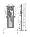
In Embodiment 4, an example of the layout of the detection circuit in FIG. 3A of Embodiment 1 will be described with reference to FIGS. 14A and 14B.
FIG. 14A is a top view of the detection circuit illustrated in FIG. 3A, and FIG. 14B is a cross-sectional view along the dashed-dotted line A1-A2 in FIG. 14A.
The detection circuit includes, over a substrate 1460 on which an insulating film 1461 is formed, a conductive film 1411 serving as the first wiring 311 (PR), a conductive film 1412 serving as the second wiring 312 (FD), a conductive film 1413 serving as the third wiring 313 (VR), a conductive film 1414 serving as the fourth wiring 314 (OUT), a conductive film 1415 serving as the fifth wiring 315 (SE), and a conductive film 1416 serving as the sixth wiring 316 (TX).
The photoelectric conversion element 300 includes a p-type semiconductor film 1401, an i-type semiconductor film 1402, and an n-type semiconductor film 1403 that are stacked in this order.
The conductive film 1411, which serves as the first wiring 311 (PR), is electrically connected to the p-type semiconductor film 1401 that functions as one of the electrodes (the anode) of the photoelectric conversion element 300.
A conductive film 1418 functions as the gate of the third transistor 303 and is electrically connected to the conductive film 1416, which serves as the sixth wiring 316 (TX).
A conductive film 1419 functions as one of the source and the drain of the third transistor 303.
A conductive film 1420 functions as the other of the source and the drain of the third transistor 303.
A conductive film 1421 is electrically connected to the n-type semiconductor film 1403 and the conductive film 1419.
A conductive film 1422 functions as the gate of the first transistor 301 and is electrically connected to the conductive film 1420. Note that the conductive films 1420 and 1422 correspond to the second wiring 312 (FD) provided in the detection circuit illustrated in FIG. 3A.
A conductive film 1423 functions as the one of the source and the drain of the first transistor 301 and is electrically connected to the conductive film 1413, which serves as the third wiring 313 (VR).
A conductive film 1424 functions as the other of the source and the drain of the first transistor 301 and one of the source and the drain of the second transistor 302.
A conductive film 1425 functions as the other of the source and the drain of the second transistor 302 and is electrically connected to the conductive film 1414, which serves as the fourth wiring 314 (OUT).
A conductive film 1426 functions as the gate of the second transistor 302 and is electrically connected to the conductive film 1415, which serves as the fifth wiring 315 (SE).
The conductive films 1413, 1414, 1418, 1422, and 1426 can be formed by processing of one conductive film formed on the insulating surface into a desired shape. A gate insulating film 1428 is formed over the conductive films 1413, 1414, 1418, 1422, and 1426. Semiconductor layers 1451 to 1453 are formed over the gate insulating film 1428. The semiconductor layers 1451 to 1453 are the semiconductor layers of the first to third transistors 301 to 303. The conductive films 1411, 1415, 1416, 1419, 1420, 1423, 1424, and 1425 can be formed by processing of one conductive film formed over the semiconductor layers 1451 to 1453 and the gate insulating film 1428 into a desired shape.
An insulating film 1481 and an insulating film 1482 are formed over the conductive films 1411, 1415, 1416, 1419, 1420, 1423, 1424, and 1425. The conductive film 1421 is formed over the insulating films 1481 and 1482.
An oxide semiconductor is preferably used for the semiconductor layer 1453 of the third transistor 303. In order for the charge accumulation portion to achieve long-term storage of charge generated by irradiation of the photoelectric conversion element 300 with light, the third transistor 303 that is electrically connected to the charge accumulation portion needs to have extremely low off-state current. For this reason, the use of an oxide semiconductor material for the semiconductor layer 1453 can improve the performance of the detection circuit. Note that the charge accumulation portion refers to the second wiring 312 (FD) in the detection circuit.
In the detection circuit, the elements such as the transistors and the photoelectric conversion element 300 may overlap each other. This structure can increase the pixel density and thus can increase the resolution of an imaging device. In addition, the area of the photoelectric conversion element 300 can be increased, and the sensitivity of the imaging device can be increased as a result.
This embodiment can be combined with any of the other embodiments disclosed in this specification as appropriate.
Embodiment 5
Embodiment 5 shows a structure of the transistor using an oxide semiconductor material for a channel formation region described in Embodiment 1, a material used for the semiconductor layer of the transistor, and a fabrication method and a structure of the semiconductor layer.
<Structure of Transistor>
For example, the transistor can have the structure illustrated in the top view and the cross-sectional view of FIGS. 14A and 14B of the third transistor 303 including the semiconductor layer 1453. This structure is an example of a channel-etched bottom-gate structure, but the transistor can have a variety of other known structures such as a channel-protective bottom-gate structure, a non-self-aligned top-gate structure, and a self-aligned top-gate structure.
<Material used for Semiconductor Layer>
An oxide semiconductor material used for the semiconductor layer preferably contains at least indium (In) or zinc (Zn). In particular, the oxide semiconductor material preferably contains In and Zn. In addition, as a stabilizer for reducing variations in electric characteristics of transistors using the oxide semiconductor material, the oxide semiconductor material preferably contains gallium (Ga), tin (Sn), hafnium (Hf), and/or aluminum (Al).
As another stabilizer, the oxide semiconductor material may contain one or plural kinds of lanthanoid such as lanthanum (La), cerium (Ce), praseodymium (Pr), neodymium (Nd), samarium (Sm), europium (Eu), gadolinium (Gd), terbium (Tb), dysprosium (Dy), holmium (Ho), erbium (Er), thulium (Tm), ytterbium (Yb), and lutetium (Lu).
Examples of the oxide semiconductor material to be used are indium oxide, tin oxide, zinc oxide, In—Zn-based oxide, In—Mg-based oxide, In—Ga-based oxide, In—Ga—Zn-based oxide (also referred to as IGZO), In—Al—Zn-based oxide, In—Sn—Zn-based oxide, In—Hf—Zn-based oxide, In—La—Zn-based oxide, In—Ce—Zn-based oxide, In—Pr—Zn-based oxide, In—Nd—Zn-based oxide, In—Sm—Zn-based oxide, In—Eu—Zn-based oxide, In—Gd—Zn-based oxide, In—Tb—Zn-based oxide, In—Dy—Zn-based oxide, In—Ho—Zn-based oxide, In—Er—Zn-based oxide, In—Tm—Zn-based oxide, In—Yb—Zn-based oxide, In—Lu—Zn-based oxide, In—Sn—Ga—Zn-based oxide, In—Hf—Ga—Zn-based oxide, In—Al—Ga—Zn-based oxide, In—Sn—Al—Zn-based oxide, In—Sn—Hf—Zn-based oxide, and In—Hf—Al—Zn-based oxide.
For example, an In—Ga—Zn-based oxide refers to an oxide containing In, Ga, and Zn as its main components, and there is no limitation on the composition ratio of In, Ga, and Zn. The In—Ga—Zn-based oxide may contain a metal element other than In, Ga, and Zn. The In—Ga—Zn-based oxide has sufficiently high resistance when no electric field is applied thereto, so that off-state current can be sufficiently reduced. Moreover, the In—Ga—Zn-based oxide has high mobility and thus is a semiconductor material suitable for a transistor in a radiation detection panel.
For example, an In—Ga—Zn-based oxide with an atomic ratio of In:Ga:Zn=1:1:1 (=1/3:1/3:1/3) or In:Ga:Zn=2:2:1 (=2/5:2/5:1/5), or an oxide with an atomic ratio close to the above atomic ratios can be used. Alternatively, an In—Sn—Zn-based oxide with an atomic ratio of In:Sn:Zn=1:1:1 (=1/3:1/3:1/3), In:Sn:Zn=2:1:3 (=1/3:1/6:1/2), or In:Sn:Zn=2:1:5 (=1/4:1/8:5/8) or an oxide with an atomic ratio close to the above atomic ratios may be used.
Alternatively, a material represented by InMO3(ZnO)m (m>0, where m is not an integer) may be used as the oxide semiconductor material. Note that M represents one or more metal elements selected from Ga, Fe, Mn, and Co. Further alternatively, a material expressed by In2SnO5(ZnO)n (n>0, where n is an integer) may be used as the oxide semiconductor material.
<Method for Forming Semiconductor Layer>
As the semiconductor layer, a film formed using an oxide semiconductor material (hereinafter referred to as an oxide semiconductor film) can be formed in the following manner, for example: an oxide semiconductor film is formed by PVD such as sputtering or electron beam evaporation; a resist mask is formed over the film by photolithography or the like; and then, the oxide semiconductor film is selectively removed by dry etching, wet etching, or the like.
Note that if the oxide semiconductor film contains a large amount of hydrogen, the hydrogen and the oxide semiconductor are bonded to each other, so that part of the hydrogen serves as a donor and causes generation of an electron which is a carrier. As a result, the threshold voltage of the transistor shifts in the negative direction. Accordingly, the hydrogen concentration in the oxide semiconductor film is preferably lower than 5×10¹⁸ atoms/cm3, more preferably 1×10¹⁸ atoms/cm3 or lower, still more preferably 5×10¹⁷ atoms/cm3 or lower, even more preferably 1×10¹⁶ atoms/cm3 or lower. Note that the hydrogen concentration in the semiconductor layer is measured by secondary ion mass spectrometry (SIMS).
For the above reason, it is preferable that the gas used for deposition of the oxide semiconductor film do not contain impurities such as water, hydrogen, a hydroxyl group, or a hydride.
For example, a deposition gas having a purity of 6N or higher, preferably 7N or higher (i.e., an impurity concentration of 1 ppm or less, preferably 0.1 ppm or less) is used. Alternatively, a deposition gas having a dew point of −80° C. or lower, preferably −100° C. or lower is preferably used.
An entrapment vacuum pump such as a cryopump, an ion pump, or a titanium sublimation pump is preferably used to remove moisture (including water, water vapor, hydrogen, a hydroxyl group, or a hydroxide) in a deposition chamber. The evacuation unit may be a turbo molecular pump provided with a cold trap. From the deposition chamber which is evacuated with a cryopump, a hydrogen atom, a compound containing a hydrogen atom such as water (H2O) (preferably, also a compound containing a carbon atom), and the like are removed, whereby the concentration of impurities such as hydrogen or moisture in the oxide semiconductor film formed in the deposition chamber can be reduced.
It is also preferable that the oxide semiconductor film contain nitrogen as little as possible. This is because nitrogen is bonded to the oxide semiconductor like hydrogen, so that part of the nitrogen serves as a donor and causes generation of an electron which is a carrier. Thus, it is preferable to use a semiconductor film having a peak of the amount of released ammonia molecules of 5.0×10²¹ molecules/cm3 or less, preferably 1.0×10²¹ molecules/cm3 or less, further preferably 8.0×10²⁰ molecules/cm3 or less when measured by TDS after the semiconductor film is heated.
Moreover, the concentration of an alkali metal or an alkaline earth metal in the oxide semiconductor film is preferably 1×10¹⁸ atoms/cm3 or lower, more preferably 2×10¹⁶ atoms/cm3 or lower. This is because carriers might be generated when an alkali metal or an alkaline earth metal is bonded to the oxide semiconductor like hydrogen and nitrogen mentioned above, leading to an increase in off-state current of the transistor.
The oxide semiconductor film is classified roughly into a single-crystal oxide semiconductor film and a non-single-crystal oxide semiconductor film. The non-single-crystal oxide semiconductor film includes any of an amorphous oxide semiconductor film, a microcrystalline oxide semiconductor film, a polycrystalline oxide semiconductor film, a c-axis aligned crystalline oxide semiconductor (CAAC-OS) film, and the like. Note that the oxide semiconductor film may be a stacked film including two or more films of an amorphous oxide semiconductor film, a microcrystalline oxide semiconductor film, and a CAAC-OS film, for example.
The amorphous oxide semiconductor film has disordered atomic arrangement and no crystalline component. A typical example of the amorphous oxide semiconductor film is an oxide semiconductor film in which no crystal part exists even in a microscopic region, and the whole of the film is amorphous.
The microcrystalline oxide semiconductor film includes a microcrystal (also referred to as nanocrystal) with a size greater than or equal to 1 nm and less than 10 nm, for example. Thus, the microcrystalline oxide semiconductor film has a higher degree of atomic order than the amorphous oxide semiconductor film. Hence, the density of defect states of the microcrystalline oxide semiconductor film is lower than that of the amorphous oxide semiconductor film.
The oxide semiconductor film is preferably a CAAC-OS (c-axis aligned crystalline oxide semiconductor) film.
The CAAC-OS film is one of oxide semiconductor films including a plurality of crystal parts, and most of the crystal parts each fit inside a cube whose one side is less than 100 nm. Thus, there is a case where a crystal part included in the CAAC-OS film fits inside a cube whose one side is less than 10 nm, less than 5 nm, or less than 3 nm. The density of defect states of the CAAC-OS film is lower than that of the microcrystalline oxide semiconductor film. The CAAC-OS film is described in detail below.
In the following description, the term “parallel” indicates that the angle formed between two straight lines is greater than or equal to −10° and less than or equal to 10°, and accordingly also includes the case where the angle is greater than or equal to −5° and less than or equal to 5°. In addition, the term “perpendicular” indicates that the angle formed between two straight lines is greater than or equal to 80° and less than or equal to 100°, and accordingly includes the case where the angle is greater than or equal to 85° and less than or equal to 95°.
In a transmission electron microscope (TEM) image of the CAAC-OS film, a boundary between crystal parts, that is, a grain boundary is not clearly observed. Thus, in the CAAC-OS film, a reduction in electron mobility due to the grain boundary is less likely to occur.
According to the TEM image of the CAAC-OS film observed in a direction substantially parallel to a sample surface (cross-sectional TEM image), metal atoms are arranged in a layered manner in the crystal parts. Each metal atom layer has a morphology reflected by a surface over which the CAAC-OS film is formed (hereinafter, a surface over which the CAAC-OS film is formed is referred to as a formation surface) or a top surface of the CAAC-OS film, and is arranged in parallel to the formation surface or the top surface of the CAAC-OS film.
On the other hand, according to the TEM image of the CAAC-OS film observed in a direction substantially perpendicular to the sample surface (plan TEM image), metal atoms are arranged in a triangular or hexagonal configuration in the crystal parts. However, there is no regularity of arrangement of metal atoms between different crystal parts.
From the results of the cross-sectional TEM image and the plan TEM image, alignment is found in the crystal parts in the CAAC-OS film.
A CAAC-OS film is subjected to structural analysis with an X-ray diffraction (XRD) apparatus. For example, when the CAAC-OS film including an InGaZnO4 crystal is analyzed by an out-of-plane method, a peak appears frequently when the diffraction angle (2θ) is around 31°. This peak is derived from the (009) plane of the InGaZnO4 crystal, which indicates that crystals in the CAAC-OS film have c-axis alignment, and that the c-axes are aligned in a direction substantially perpendicular to the formation surface or the top surface of the CAAC-OS film.
On the other hand, when the CAAC-OS film is analyzed by an in-plane method in which an X-ray enters a sample in a direction substantially perpendicular to the c-axis, a peak appears frequently when 2θ is around 56°. This peak is derived from the (110) plane of the InGaZnO4 crystal. Here, analysis (φ scan) is performed under conditions where the sample is rotated around a normal vector of a sample surface as an axis (φ axis) with 2θ fixed at around 56°. In the case where the sample is a single-crystal oxide semiconductor film of InGaZnO4, six peaks appear. The six peaks are derived from crystal planes equivalent to the (110) plane. On the other hand, in the case of a CAAC-OS film, a peak is not clearly observed even when φ scan is performed with 2θ fixed at around 56°.
According to the above results, in the CAAC-OS film having c-axis alignment, while the directions of a-axes and b-axes are different between crystal parts, the c-axes are aligned in a direction parallel to a normal vector of a formation surface or a normal vector of a top surface. Thus, each metal atom layer arranged in a layered manner observed in the cross-sectional TEM image corresponds to a plane parallel to the a-b plane of the crystal.
Note that the crystal part is formed concurrently with deposition of the CAAC-OS film or is formed through crystallization treatment such as heat treatment. As described above, the c-axis of the crystal is aligned in a direction parallel to a normal vector of a formation surface or a normal vector of a top surface. Thus, for example, in the case where the shape of the CAAC-OS film is changed by etching or the like, the c-axis might not be necessarily parallel to a normal vector of a formation surface or a normal vector of a top surface of the CAAC-OS film.
The degree of crystallinity in the CAAC-OS film is not necessarily uniform. For example, in the case where crystal growth leading to the CAAC-OS film occurs from the vicinity of the top surface of the film, the degree of the crystallinity in the vicinity of the top surface is higher than that in the vicinity of the formation surface in some cases. Further, when an impurity is added to the CAAC-OS film, the crystallinity in a region to which the impurity is added is changed, and the degree of crystallinity in the CAAC-OS film varies depending on regions.
Note that when the CAAC-OS film with an InGaZnO4 crystal is analyzed by an out-of-plane method, a peak of 2θ may also be observed at around 36°, in addition to the peak of 2θ at around 31°. The peak of 2θ at around 36° indicates that a crystal having no c-axis alignment is included in part of the CAAC-OS film. It is preferable that in the CAAC-OS film, a peak of 2θ appear at around 31° and a peak of 2θ do not appear at around 36°.
With the use of the CAAC-OS film in a transistor, change in electric characteristics of the transistor due to irradiation with visible light or ultraviolet light is small. Thus, the transistor has high reliability.
For example, the CAAC-OS film is formed by sputtering with a polycrystalline oxide semiconductor sputtering target. By collision of ions with the sputtering target, a crystal region included in the sputtering target may be cleaved along an a-b plane and sputtered particles having a plane parallel to the a-b plane (flat-plate-like sputtered particles or pellet-like sputtered particles) may flake off from the sputtering target. In this case, the flat-plate-like (or pellet-like) sputtered particles reach a substrate while maintaining their crystal state, whereby the CAAC-OS film can be formed.
For the deposition of the CAAC-OS film, the following conditions are preferably used.
Decay of the crystal state due to impurities can be prevented by reducing the amount of impurities entering the CAAC-OS film during the deposition, for example, by reduction in the concentration of impurities (e.g., hydrogen, water, carbon dioxide, and nitrogen) in the deposition chamber or in a deposition gas. Specifically, a deposition gas with a dew point of −80° C. or lower, preferably −100° C. or lower is used.
With higher substrate heating temperature during the deposition, migration of sputtered particles is likely to occur after the sputtered particles reach a substrate surface. Specifically, the substrate heating temperature during the deposition ranges from 100° C. to 740° C., preferably from 150° C. to 500° C. By increase in the substrate heating temperature during the deposition, when the flat-plate-like sputtered particle reaches the substrate, migration occurs on the substrate surface, so that a flat plane of the flat-plate-like sputtered particle is attached to the substrate.
It is preferable that the proportion of oxygen in the deposition gas be increased and the power be optimized in order to reduce plasma damage at the deposition. The proportion of oxygen in the deposition gas is 30 vol % or higher, preferably 100 vol %. A higher proportion of oxygen contained in the deposition gas facilitates formation of the CAAC-OS film because an unnecessary atom (e.g., a rare gas atom) does not enter the CAAC-OS film.
As an example of the sputtering target, an In—Ga—Zn—O compound target will be described below.
A polycrystalline In—Ga—Zn—O compound target is made by mixing InOX powder, GaOY powder, and ZnOZ powder at a predetermined molar ratio, applying pressure to the mixture, and then performing heat treatment on the mixture at temperatures ranging from 1000° C. to 1500° C. Note that X, Y, and Z are each a given positive number. Here, the predetermined molar ratio of InOX powder to GaOY powder and ZnOZ powder is, for example, 2:2:1, 8:4:3, 3:1:1, 1:1:1, 4:2:3, or 3:1:2. The kinds of powder and the molar ratio for mixing the powder can be determined as appropriate depending on the intended sputtering target.
<Structure of Semiconductor Layer>
The semiconductor layer may be a single-layer oxide semiconductor film formed using the material and the method described above, or a stack of a plurality of such oxide semiconductor films. For example, the semiconductor layer may be a stack of a first oxide semiconductor film, a second oxide semiconductor film, and a third oxide semiconductor film that have different compositions.
For example, it is possible that the first, second, and third oxide semiconductor films are formed using the same constituent elements and have different compositions. For example, the first oxide semiconductor film and the third oxide semiconductor film may have an atomic ratio of In:Ga:Zn=1:1:1, and the second oxide semiconductor film may have an atomic ratio of In:Ga:Zn=3:1:2. Alternatively, the first oxide semiconductor film and the third oxide semiconductor film may have an atomic ratio of In:Ga:Zn=1:3:2, and the second oxide semiconductor film may have an atomic ratio of In:Ga:Zn=3:1:2.
At this time, the second oxide semiconductor film preferably contains more In than Ga (In>Ga). Further, the first oxide semiconductor film and the third oxide semiconductor film preferably contain In and Ga at a proportion of In≦Ga.
In an oxide semiconductor, the s orbital of heavy metal mainly contributes to carrier transfer, and overlap of the s orbitals is likely to increase when the In content in the oxide semiconductor is increased. Therefore, an oxide having a composition of In>Ga has higher mobility than an oxide having a composition of In≦Ga. Further, the formation energy of oxygen vacancy is larger and thus oxygen vacancy is less likely to occur in Ga than in In; thus, the oxide having a composition of In≦Ga has more stable characteristics than the oxide having a composition of In>Ga.
Note that when the film that is different from the oxide semiconductor film and is in contact with the oxide semiconductor film (in FIG. 14B, the insulating film 1481 and the gate insulating film 1428, for example) is provided, impurities might be diffused into the oxide semiconductor film from the film in contact with the oxide semiconductor film. For example, if silicon, carbon, or the like contained in the insulating film 1481 or the gate insulating film 1428 is diffused into the oxide semiconductor film, electric characteristics of the transistor may be adversely affected.
However, the oxide semiconductor film has the stacked structure as described above. Specifically, an oxide semiconductor film (i.e., an oxide semiconductor film having a composition of In≦Ga, which corresponds to the first oxide semiconductor film and the third oxide semiconductor film in this embodiment) having fewer oxygen vacancies and more stable characteristics than a high-mobility oxide semiconductor film (i.e., an oxide semiconductor film having a composition of In>Ga, which corresponds to the second oxide semiconductor film in this embodiment) is formed in contact with the high-mobility oxide semiconductor film so that the high-mobility oxide semiconductor film can keep a distance from the film in contact with the oxide semiconductor film (in FIG. 14B, the insulating film 1481, the gate insulating film 1428, or the like). Consequently, adverse effect of impurity diffusion on the electric characteristics of the transistor (e.g., a reduction in mobility) can be suppressed. Thus, the mobility and reliability of the transistor can be increased.
With the use of a transistor including a semiconductor layer formed using the oxide semiconductor film described in this embodiment for at least some of the transistors in the detection circuit 110, first data and second data generated based on the amount of light incident from the conversion unit 101 can be held in the first output circuit 111 and the second output circuit 112, respectively. Thus, the radiation detection panel 100 can output signals for generating an accurate pixel signal regardless of the performance of the conversion unit 101.
This embodiment can be implemented in appropriate combination with the structures described in any of the other embodiments.
This application is based on Japanese Patent Application serial No. 2012-184985 filed with Japan Patent Office on Aug. 24, 2012, the entire contents of which are hereby incorporated by reference.

Claims (20)

What is claimed is:
1. An imaging device comprising:
a detection unit;
a conversion unit; and
a radiation source,
wherein the conversion unit is configured to convert radiation from the radiation source into light,
wherein the detection unit comprises a plurality of detection circuits each comprising a first output circuit and a second output circuit,
wherein each of the first output circuit and the second output circuit comprises a photoelectric conversion element configured to generate charge in response to light incident from the conversion unit,
wherein the first output circuit is configured to generate first data corresponding to an amount of charge generated by the photoelectric conversion element when radiation is not emitted from the radiation source, and hold the first data,
wherein the second output circuit is configured to generate second data corresponding to an amount of charge generated by the photoelectric conversion element when radiation is emitted from the radiation source, and hold the second data, and
wherein the detection unit is configured to output a first signal corresponding to the first data and a second signal corresponding to the second data from each of the detection circuits.
2. The imaging device according to claim 1,
wherein each of the first output circuit and the second output circuit comprises a first transistor and a second transistor,
wherein the first transistor of the first output circuit is configured to hold potential of a gate of the second transistor of the first output circuit corresponding to the first data,
wherein the first transistor of the second output circuit is configured to hold potential of a gate of the second transistor of the second output circuit corresponding to the second data, and
wherein the first transistor of each of the first output circuit and the second output circuit comprises a channel formation region comprising an oxide semiconductor material.
3. The imaging device according to claim 1,
wherein the first output circuit and the second output circuit are provided adjacent to each other in each of the detection circuits.
4. The imaging device according to claim 1,
wherein the first output circuit and the second output circuit are provided adjacent in an oblique direction in each of the detection circuits.
5. The imaging device according to claim 1,
wherein the length of a time for the first output circuit to detect light is smaller than or equal to the length of a time for the second output circuit to detect light.
6. The imaging device according to claim 1,
wherein each of the first output circuit and the second output circuit comprises a transistor comprising a channel formation region comprising an oxide semiconductor material.
7. The imaging device according to claim 1,
wherein the radiation source is an X-ray radiation source, and
wherein the conversion unit is a scintillator converting X-rays into visible light.
8. An imaging device comprising:
a detection unit; and
a conversion unit,
wherein the conversion unit is configured to convert radiation from a radiation source into light,
wherein the detection unit comprises a plurality of detection circuits each comprising a first output circuit and a second output circuit,
wherein each of the first output circuit and the second output circuit comprises a photoelectric conversion element configured to generate charge in response to light incident from the conversion unit,
wherein the first output circuit is configured to generate first data corresponding to an amount of light incident from the conversion unit when radiation is not emitted from the radiation source, and hold the first data,
wherein the second output circuit is configured to generate second data corresponding to an amount of light incident from the conversion unit when radiation is emitted from the radiation source, and hold the second data, and
wherein the detection unit is configured to output a first signal corresponding to the first data and a second signal corresponding to the second data from each of the detection circuits.
9. The imaging device according to claim 8,
wherein each of the first output circuit and the second output circuit comprises a first transistor and a second transistor,
wherein the first transistor of the first output circuit is configured to hold potential of a gate of the second transistor of the first output circuit corresponding to the first data,
wherein the first transistor of the second output circuit is configured to hold potential of a gate of the second transistor of the second output circuit corresponding to the second data, and
wherein the first transistor of each of the first output circuit and the second output circuit comprises a channel formation region comprising an oxide semiconductor material.
10. The imaging device according to claim 8,
wherein the first output circuit and the second output circuit are provided adjacent to each other in each of the detection circuits.
11. The imaging device according to claim 8,
wherein the first output circuit and the second output circuit are provided adjacent in an oblique direction in each of the detection circuits.
12. The imaging device according to claim 8,
wherein the length of a time for the first output circuit to detect light is smaller than or equal to the length of a time for the second output circuit to detect light.
13. The imaging device according to claim 8,
wherein each of the first output circuit and the second output circuit comprises a transistor comprising a channel formation region comprising an oxide semiconductor material.
14. The imaging device according to claim 8,
wherein the radiation source is an X-ray radiation source, and
wherein the conversion unit is a scintillator converting X-rays into visible light.
15. An imaging device comprising:
a detection unit,
wherein the detection unit comprises a plurality of detection circuits each comprising a first output circuit and a second output circuit,
wherein each of the first output circuit and the second output circuit comprises a photoelectric conversion element configured to generate charge in response to light incident from a conversion unit configured to convert radiation from a radiation source into the light,
wherein the first output circuit is configured to generate first data corresponding to an amount of light incident from the conversion unit when radiation is not emitted from the radiation source, and hold the first data,
wherein the second output circuit is configured to generate second data corresponding to an amount of light incident from the conversion unit when radiation is emitted from the radiation source, and hold the second data, and
wherein the detection unit is configured to output a first signal corresponding to the first data and a second signal corresponding to the second data from each of the detection circuits.
16. The imaging device according to claim 15,
wherein the first output circuit and the second output circuit are provided adjacent to each other in each of the detection circuits.
17. The imaging device according to claim 15,
wherein the first output circuit and the second output circuit are provided adjacent in an oblique direction in each of the detection circuits.
18. The imaging device according to claim 15,
wherein the length of a time for the first output circuit to detect light is smaller than or equal to the length of a time for the second output circuit to detect light.
19. The imaging device according to claim 15,
wherein each of the first output circuit and the second output circuit comprises a transistor comprising a channel formation region comprising an oxide semiconductor material.
20. The imaging device according to claim 15,
wherein the radiation source is an X-ray radiation source, and
wherein the conversion unit is a scintillator converting X-rays into visible light.
US13/959,778 2012-08-24 2013-08-06 Radiation detection panel, radiation imaging device, and diagnostic imaging device Expired - Fee Related US9204849B2 (en)

Applications Claiming Priority (2)

Application Number Priority Date Filing Date Title
JP2012184985 2012-08-24
JP2012-184985 2012-08-24

Publications (2)

Publication Number Publication Date
US20140056405A1 US20140056405A1 (en) 2014-02-27
US9204849B2 true US9204849B2 (en) 2015-12-08

Family

ID=50147992

Family Applications (1)

Application Number Title Priority Date Filing Date
US13/959,778 Expired - Fee Related US9204849B2 (en) 2012-08-24 2013-08-06 Radiation detection panel, radiation imaging device, and diagnostic imaging device

Country Status (5)

Country Link
US (1) US9204849B2 (en)
JP (1) JP6151126B2 (en)
KR (1) KR102069683B1 (en)
DE (1) DE102013216406B4 (en)
TW (1) TWI593990B (en)

Cited By (4)

* Cited by examiner, † Cited by third party
Publication number Priority date Publication date Assignee Title
US10200573B2 (en) 2015-06-08 2019-02-05 Semiconductor Energy Laboratory Co., Ltd. Imaging device, operation method thereof, and electronic device
US10357214B2 (en) * 2013-04-26 2019-07-23 Toshiba Medical Systems Corporation Photon counting CT apparatus, light detection device, radiation detection device, and radiation analysis device
US20190242835A1 (en) * 2018-02-05 2019-08-08 Rhombus Holdings Llc Component configuration for a robust tunable sensor system for a high radiation environment
US11925497B2 (en) 2021-09-01 2024-03-12 Mazor Robotics Ltd. Systems, methods, and devices for multiple exposures imaging

Families Citing this family (13)

* Cited by examiner, † Cited by third party
Publication number Priority date Publication date Assignee Title
DE102013217278B4 (en) * 2012-09-12 2017-03-30 Semiconductor Energy Laboratory Co., Ltd. A photodetector circuit, an imaging device, and a method of driving a photodetector circuit
TWI635750B (en) 2013-08-02 2018-09-11 半導體能源研究所股份有限公司 Imaging device and operation method thereof
US9360564B2 (en) 2013-08-30 2016-06-07 Semiconductor Energy Laboratory Co., Ltd. Imaging device
US9674470B2 (en) 2014-04-11 2017-06-06 Semiconductor Energy Laboratory Co., Ltd. Semiconductor device, method for driving semiconductor device, and method for driving electronic device
KR20220100106A (en) 2014-06-09 2022-07-14 가부시키가이샤 한도오따이 에네루기 켄큐쇼 Imaging device
TW202243228A (en) 2014-06-27 2022-11-01 日商半導體能源研究所股份有限公司 Imaging device and electronic device
US9729809B2 (en) 2014-07-11 2017-08-08 Semiconductor Energy Laboratory Co., Ltd. Semiconductor device and driving method of semiconductor device or electronic device
US10126433B2 (en) 2014-11-10 2018-11-13 Halliburton Energy Services, Inc. Energy detection apparatus, methods, and systems
WO2018201308A1 (en) 2017-05-03 2018-11-08 Shenzhen Xpectvision Technology Co., Ltd. Method of making radiation detector
KR102637438B1 (en) 2017-06-27 2024-02-15 가부시키가이샤 한도오따이 에네루기 켄큐쇼 Semiconductor devices and electronic components
WO2019084704A1 (en) * 2017-10-30 2019-05-09 Shenzhen Xpectvision Technology Co., Ltd. Dark noise compensation in radiation detector
WO2021016747A1 (en) * 2019-07-26 2021-02-04 Shenzhen Xpectvision Technology Co., Ltd. Radiation detector with scintillator
CN117740145A (en) * 2022-09-15 2024-03-22 无锡中科德芯感知科技有限公司 Linear photoelectric focal plane detector and manufacturing method thereof

Citations (123)

* Cited by examiner, † Cited by third party
Publication number Priority date Publication date Assignee Title
JPS60198861A (en) 1984-03-23 1985-10-08 Fujitsu Ltd Thin film transistor
JPS63210023A (en) 1987-02-24 1988-08-31 Natl Inst For Res In Inorg Mater Compound having laminar structure of hexagonal crystal system expressed by ingazn4o7 and its production
JPS63210022A (en) 1987-02-24 1988-08-31 Natl Inst For Res In Inorg Mater Compound having laminar structure of hexagonal crystal system expressed by ingazn3o6 and its production
JPS63210024A (en) 1987-02-24 1988-08-31 Natl Inst For Res In Inorg Mater Compound having laminar structure of hexagonal crystal system expressed by ingazn5o8 and its production
JPS63215519A (en) 1987-02-27 1988-09-08 Natl Inst For Res In Inorg Mater Chemical compound of ingazn6o9 with hexagonal system layer structure
JPS63239117A (en) 1987-01-28 1988-10-05 Natl Inst For Res In Inorg Mater Compound having lamellar structure of hexagonal system expressed in ingazn2o5 and its production
JPS63265818A (en) 1987-04-22 1988-11-02 Natl Inst For Res In Inorg Mater Compound having hexagonal laminar structure expressed by ingazn7o10 and its production
JPH05251705A (en) 1992-03-04 1993-09-28 Fuji Xerox Co Ltd Thin-film transistor
JPH08264794A (en) 1995-03-27 1996-10-11 Res Dev Corp Of Japan Metal oxide semiconductor device forming a pn junction with a thin film transistor of metal oxide semiconductor of copper suboxide and manufacture thereof
US5731856A (en) 1995-12-30 1998-03-24 Samsung Electronics Co., Ltd. Methods for forming liquid crystal displays including thin film transistors and gate pads having a particular structure
US5731613A (en) 1994-08-19 1998-03-24 Semiconductor Energy Laboratory Co., Ltd. Semiconductor device having a monocrystalline layer composed of carbon, oxygen, hydrogen and nitrogen atoms
US5744864A (en) 1995-08-03 1998-04-28 U.S. Philips Corporation Semiconductor device having a transparent switching element
US5923722A (en) * 1996-08-05 1999-07-13 Siemens Aktiengesellschaft X-ray diagnostic apparatus with control of x-ray emission dependent on the afterglow in the solid-state detector
JPH11316428A (en) 1998-01-30 1999-11-16 Konica Corp Method and system for forming x-ray image
JP2000044236A (en) 1998-07-24 2000-02-15 Hoya Corp Article having transparent conductive oxide thin film and its production
US6025607A (en) 1996-05-08 2000-02-15 Semiconductor Energy Laboratory Co., Ltd. Thin-film transistor and liquid crystal display device
JP2000150900A (en) 1998-11-17 2000-05-30 Japan Science & Technology Corp Transistor and semiconductor device
US6198799B1 (en) 1998-01-30 2001-03-06 Konica Corporation X-ray image forming method and x-ray image forming system
US6294274B1 (en) 1998-11-16 2001-09-25 Tdk Corporation Oxide thin film
US20010046027A1 (en) 1999-09-03 2001-11-29 Ya-Hsiang Tai Liquid crystal display having stripe-shaped common electrodes formed above plate-shaped pixel electrodes
JP2002076356A (en) 2000-09-01 2002-03-15 Japan Science & Technology Corp Semiconductor device
US20020056838A1 (en) 2000-11-15 2002-05-16 Matsushita Electric Industrial Co., Ltd. Thin film transistor array, method of producing the same, and display panel using the same
US20020132454A1 (en) 2001-03-19 2002-09-19 Fuji Xerox Co., Ltd. Method of forming crystalline semiconductor thin film on base substrate, lamination formed with crystalline semiconductor thin film and color filter
JP2002289859A (en) 2001-03-23 2002-10-04 Minolta Co Ltd Thin-film transistor
JP2003086000A (en) 2001-09-10 2003-03-20 Sharp Corp Semiconductor memory and its test method
JP2003086808A (en) 2001-09-10 2003-03-20 Masashi Kawasaki Thin film transistor and matrix display
US20030189401A1 (en) 2002-03-26 2003-10-09 International Manufacturing And Engineering Services Co., Ltd. Organic electroluminescent device
US20030218222A1 (en) 2002-05-21 2003-11-27 The State Of Oregon Acting And Through The Oregon State Board Of Higher Education On Behalf Of Transistor structures and methods for making the same
US20040038446A1 (en) 2002-03-15 2004-02-26 Sanyo Electric Co., Ltd.- Method for forming ZnO film, method for forming ZnO semiconductor layer, method for fabricating semiconductor device, and semiconductor device
JP2004103957A (en) 2002-09-11 2004-04-02 Japan Science & Technology Corp Transparent thin film field effect type transistor using homologous thin film as active layer
US6747638B2 (en) 2000-01-31 2004-06-08 Semiconductor Energy Laboratory Co., Ltd. Adhesion type area sensor and display device having adhesion type area sensor
US20040127038A1 (en) 2002-10-11 2004-07-01 Carcia Peter Francis Transparent oxide semiconductor thin film transistors
JP2004273732A (en) 2003-03-07 2004-09-30 Sharp Corp Active matrix substrate and its producing process
JP2004273614A (en) 2003-03-06 2004-09-30 Sharp Corp Semiconductor device and its fabricating process
WO2004114391A1 (en) 2003-06-20 2004-12-29 Sharp Kabushiki Kaisha Semiconductor device, its manufacturing method, and electronic device
US20050017302A1 (en) 2003-07-25 2005-01-27 Randy Hoffman Transistor including a deposited channel region having a doped portion
US20050199959A1 (en) 2004-03-12 2005-09-15 Chiang Hai Q. Semiconductor device
US20060043377A1 (en) 2004-03-12 2006-03-02 Hewlett-Packard Development Company, L.P. Semiconductor device
US20060091793A1 (en) 2004-11-02 2006-05-04 3M Innovative Properties Company Methods and displays utilizing integrated zinc oxide row and column drivers in conjunction with organic light emitting diodes
US20060110867A1 (en) 2004-11-10 2006-05-25 Canon Kabushiki Kaisha Field effect transistor manufacturing method
US20060108529A1 (en) 2004-11-10 2006-05-25 Canon Kabushiki Kaisha Sensor and image pickup device
US20060108636A1 (en) 2004-11-10 2006-05-25 Canon Kabushiki Kaisha Amorphous oxide and field effect transistor
US20060113539A1 (en) 2004-11-10 2006-06-01 Canon Kabushiki Kaisha Field effect transistor
US20060113536A1 (en) 2004-11-10 2006-06-01 Canon Kabushiki Kaisha Display
US20060113549A1 (en) 2004-11-10 2006-06-01 Canon Kabushiki Kaisha Light-emitting device
US20060113565A1 (en) 2004-11-10 2006-06-01 Canon Kabushiki Kaisha Electric elements and circuits utilizing amorphous oxides
US7061014B2 (en) 2001-11-05 2006-06-13 Japan Science And Technology Agency Natural-superlattice homologous single crystal thin film, method for preparation thereof, and device using said single crystal thin film
US20060157760A1 (en) 2005-01-04 2006-07-20 Sony Corporation Imaging apparatus and imaging method
US20060169973A1 (en) 2005-01-28 2006-08-03 Semiconductor Energy Laboratory Co., Ltd. Semiconductor device, electronic device, and method of manufacturing semiconductor device
US20060170111A1 (en) 2005-01-28 2006-08-03 Semiconductor Energy Laboratory Co., Ltd. Semiconductor device, electronic device, and method of manufacturing semiconductor device
US20060197092A1 (en) 2005-03-03 2006-09-07 Randy Hoffman System and method for forming conductive material on a substrate
US7105868B2 (en) 2002-06-24 2006-09-12 Cermet, Inc. High-electron mobility transistor with zinc oxide
US20060208977A1 (en) 2005-03-18 2006-09-21 Semiconductor Energy Laboratory Co., Ltd. Semiconductor device, and display device, driving method and electronic apparatus thereof
US20060228974A1 (en) 2005-03-31 2006-10-12 Theiss Steven D Methods of making displays
US20060231882A1 (en) 2005-03-28 2006-10-19 Il-Doo Kim Low voltage flexible organic/transparent transistor for selective gas sensing, photodetecting and CMOS device applications
US20060238135A1 (en) 2005-04-20 2006-10-26 Semiconductor Energy Laboratory Co., Ltd. Semiconductor device and display device
US20060284172A1 (en) 2005-06-10 2006-12-21 Casio Computer Co., Ltd. Thin film transistor having oxide semiconductor layer and manufacturing method thereof
US20060284171A1 (en) 2005-06-16 2006-12-21 Levy David H Methods of making thin film transistors comprising zinc-oxide-based semiconductor materials and transistors made thereby
US20060292777A1 (en) 2005-06-27 2006-12-28 3M Innovative Properties Company Method for making electronic devices using metal oxide nanoparticles
US20070018075A1 (en) 2005-07-21 2007-01-25 Stmicroelectronics S.A. Image sensor
US20070024187A1 (en) 2005-07-28 2007-02-01 Shin Hyun S Organic light emitting display (OLED) and its method of fabrication
US20070046191A1 (en) 2005-08-23 2007-03-01 Canon Kabushiki Kaisha Organic electroluminescent display device and manufacturing method thereof
US20070054507A1 (en) 2005-09-06 2007-03-08 Canon Kabushiki Kaisha Method of fabricating oxide semiconductor device
US20070052025A1 (en) 2005-09-06 2007-03-08 Canon Kabushiki Kaisha Oxide semiconductor thin film transistor and method of manufacturing the same
US20070090365A1 (en) 2005-10-20 2007-04-26 Canon Kabushiki Kaisha Field-effect transistor including transparent oxide and light-shielding member, and display utilizing the transistor
US7211825B2 (en) 2004-06-14 2007-05-01 Yi-Chi Shih Indium oxide-based thin film transistors and circuits
US20070108446A1 (en) 2005-11-15 2007-05-17 Semiconductor Energy Laboratory Co., Ltd. Semiconductor device and manufacturing method thereof
US20070152217A1 (en) 2005-12-29 2007-07-05 Chih-Ming Lai Pixel structure of active matrix organic light-emitting diode and method for fabricating the same
US20070172591A1 (en) 2006-01-21 2007-07-26 Samsung Electronics Co., Ltd. METHOD OF FABRICATING ZnO FILM AND THIN FILM TRANSISTOR ADOPTING THE ZnO FILM
US20070187760A1 (en) 2006-02-02 2007-08-16 Kochi Industrial Promotion Center Thin film transistor including low resistance conductive thin films and manufacturing method thereof
US20070187678A1 (en) 2006-02-15 2007-08-16 Kochi Industrial Promotion Center Semiconductor device including active layer made of zinc oxide with controlled orientations and manufacturing method thereof
US20070194379A1 (en) 2004-03-12 2007-08-23 Japan Science And Technology Agency Amorphous Oxide And Thin Film Transistor
US7271835B2 (en) 2002-09-18 2007-09-18 Sony Corporation Solid-state image pickup device and device driving control method for solid-state image pickup
US20070252928A1 (en) 2006-04-28 2007-11-01 Toppan Printing Co., Ltd. Structure, transmission type liquid crystal display, reflection type display and manufacturing method thereof
US7297977B2 (en) 2004-03-12 2007-11-20 Hewlett-Packard Development Company, L.P. Semiconductor device
US20070272922A1 (en) 2006-04-11 2007-11-29 Samsung Electronics Co. Ltd. ZnO thin film transistor and method of forming the same
US20070287296A1 (en) 2006-06-13 2007-12-13 Canon Kabushiki Kaisha Dry etching method for oxide semiconductor film
US20080006877A1 (en) 2004-09-17 2008-01-10 Peter Mardilovich Method of Forming a Solution Processed Device
US7323356B2 (en) 2002-02-21 2008-01-29 Japan Science And Technology Agency LnCuO(S,Se,Te)monocrystalline thin film, its manufacturing method, and optical device or electronic device using the monocrystalline thin film
US20080038882A1 (en) 2006-08-09 2008-02-14 Kazushige Takechi Thin-film device and method of fabricating the same
US20080038929A1 (en) 2006-08-09 2008-02-14 Canon Kabushiki Kaisha Method of dry etching oxide semiconductor film
US20080050595A1 (en) 2006-01-11 2008-02-28 Murata Manufacturing Co., Ltd. Transparent conductive film and method for manufacturing the same
US20080054319A1 (en) 2006-08-31 2008-03-06 Micron Technology, Inc. Transparent-channel thin-film transistor-based pixels for high-performance image sensors
US20080073653A1 (en) 2006-09-27 2008-03-27 Canon Kabushiki Kaisha Semiconductor apparatus and method of manufacturing the same
US20080083950A1 (en) 2006-10-10 2008-04-10 Alfred I-Tsung Pan Fused nanocrystal thin film semiconductor and method
US20080106191A1 (en) 2006-09-27 2008-05-08 Seiko Epson Corporation Electronic device, organic electroluminescence device, and organic thin film semiconductor device
US20080129195A1 (en) 2006-12-04 2008-06-05 Toppan Printing Co., Ltd. Color el display and method for producing the same
US20080128689A1 (en) 2006-11-29 2008-06-05 Je-Hun Lee Flat panel displays comprising a thin-film transistor having a semiconductive oxide in its channel and methods of fabricating the same for use in flat panel displays
US7385224B2 (en) 2004-09-02 2008-06-10 Casio Computer Co., Ltd. Thin film transistor having an etching protection film and manufacturing method thereof
US20080166834A1 (en) 2007-01-05 2008-07-10 Samsung Electronics Co., Ltd. Thin film etching method
US7402506B2 (en) 2005-06-16 2008-07-22 Eastman Kodak Company Methods of making thin film transistors comprising zinc-oxide-based semiconductor materials and transistors made thereby
US20080182358A1 (en) 2007-01-26 2008-07-31 Cowdery-Corvan Peter J Process for atomic layer deposition
US7411209B2 (en) 2006-09-15 2008-08-12 Canon Kabushiki Kaisha Field-effect transistor and method for manufacturing the same
US20080224133A1 (en) 2007-03-14 2008-09-18 Jin-Seong Park Thin film transistor and organic light-emitting display device having the thin film transistor
US20080258143A1 (en) 2007-04-18 2008-10-23 Samsung Electronics Co., Ltd. Thin film transitor substrate and method of manufacturing the same
US20080258139A1 (en) 2007-04-17 2008-10-23 Toppan Printing Co., Ltd. Structure with transistor
US20080258141A1 (en) 2007-04-19 2008-10-23 Samsung Electronics Co., Ltd. Thin film transistor, method of manufacturing the same, and flat panel display having the same
US20080258140A1 (en) 2007-04-20 2008-10-23 Samsung Electronics Co., Ltd. Thin film transistor including selectively crystallized channel layer and method of manufacturing the thin film transistor
US7453087B2 (en) 2005-09-06 2008-11-18 Canon Kabushiki Kaisha Thin-film transistor and thin-film diode having amorphous-oxide semiconductor layer
US20080296568A1 (en) 2007-05-29 2008-12-04 Samsung Electronics Co., Ltd Thin film transistors and methods of manufacturing the same
US7465958B2 (en) 2004-03-12 2008-12-16 Semiconductor Energy Laboratory Co., Ltd. Thin film transistor, semiconductor device, and method for manufacturing the same
US7501293B2 (en) 2002-06-13 2009-03-10 Murata Manufacturing Co., Ltd. Semiconductor device in which zinc oxide is used as a semiconductor material and method for manufacturing the semiconductor device
US20090073325A1 (en) 2005-01-21 2009-03-19 Semiconductor Energy Laboratory Co., Ltd. Semiconductor device and method for manufacturing the same, and electric device
US20090101948A1 (en) 2007-10-19 2009-04-23 Samsung Electronics Co., Ltd. CMOS image sensors having transparent transistors and methods of manufacturing the same
US20090114910A1 (en) 2005-09-06 2009-05-07 Canon Kabushiki Kaisha Semiconductor device
US20090134399A1 (en) 2005-02-18 2009-05-28 Semiconductor Energy Laboratory Co., Ltd. Semiconductor Device and Method for Manufacturing the Same
US20090152541A1 (en) 2005-02-03 2009-06-18 Semiconductor Energy Laboratory Co., Ltd. Electronic device, semiconductor device and manufacturing method thereof
US20090152506A1 (en) 2007-12-17 2009-06-18 Fujifilm Corporation Process for producing oriented inorganic crystalline film, and semiconductor device using the oriented inorganic crystalline film
US7674650B2 (en) 2005-09-29 2010-03-09 Semiconductor Energy Laboratory Co., Ltd. Semiconductor device and manufacturing method thereof
US20100065844A1 (en) 2008-09-18 2010-03-18 Sony Corporation Thin film transistor and method of manufacturing thin film transistor
US20100092800A1 (en) 2008-10-09 2010-04-15 Canon Kabushiki Kaisha Substrate for growing wurtzite type crystal and method for manufacturing the same and semiconductor device
US20100109002A1 (en) 2007-04-25 2010-05-06 Canon Kabushiki Kaisha Oxynitride semiconductor
US20100117991A1 (en) 2008-11-07 2010-05-13 Semiconductor Energy Laboratory Co., Ltd. Image input-output device
US20100182282A1 (en) 2009-01-21 2010-07-22 Semiconductor Energy Laboratory Co., Ltd. Touch panel and electronic device
US20110176038A1 (en) 2010-01-15 2011-07-21 Semiconductor Energy Laboratory Co., Ltd. Semiconductor device and method for driving the same
US20110215323A1 (en) 2010-03-08 2011-09-08 Semiconductor Energy Laboratory Co., Ltd. Semiconductor device and manufacturing method thereof
US20110220889A1 (en) 2010-03-12 2011-09-15 Semiconductor Energy Laboratory Co., Ltd. Semiconductor device
US20110221723A1 (en) 2010-03-12 2011-09-15 Semiconductor Energy Laboratory Co., Ltd. Driving method of display device
US20120001076A1 (en) * 2009-03-26 2012-01-05 Koninklijke Philips Electronics N.V. Data acquisition
US20120002090A1 (en) 2010-07-01 2012-01-05 Semiconductor Energy Laboratory Co., Ltd. Solid-state imaging device and semiconductor display device
US20120056861A1 (en) 2010-09-08 2012-03-08 Semiconductor Energy Laboratory Co., Ltd. Semiconductor device
US20120146027A1 (en) 2010-12-09 2012-06-14 Semiconductor Energy Laboratory Co., Ltd. Photodetector circuit, input device, and input/output device
US20130083227A1 (en) * 2010-05-27 2013-04-04 Panasonic Corporation Solid-state image capturing element and method for driving solid-state image capturing element

Family Cites Families (10)

* Cited by examiner, † Cited by third party
Publication number Priority date Publication date Assignee Title
KR100246358B1 (en) * 1997-09-25 2000-03-15 김영환 Active pixel sensor with electronic shutter
JP3868621B2 (en) * 1998-03-17 2007-01-17 株式会社東芝 Image acquisition apparatus, image acquisition method, and recording medium
JP4965931B2 (en) * 2005-08-17 2012-07-04 キヤノン株式会社 Radiation imaging apparatus, radiation imaging system, control method thereof, and control program
JP4882404B2 (en) * 2006-02-14 2012-02-22 株式会社島津製作所 Radiation imaging apparatus and radiation detection signal processing method
JP5043448B2 (en) * 2006-03-10 2012-10-10 キヤノン株式会社 Radiation imaging apparatus and radiation imaging system
JP2009082194A (en) * 2007-09-27 2009-04-23 Fujifilm Corp Radiation conversion panel and method of capturing radiation image with it
JP5672853B2 (en) * 2010-08-25 2015-02-18 ソニー株式会社 Radiation imaging device
KR101372637B1 (en) * 2010-09-06 2014-03-10 가부시키가이샤 시마쓰세사쿠쇼 Radiation detector
JP5830867B2 (en) * 2011-02-03 2015-12-09 ソニー株式会社 Radiation imaging apparatus and radiation imaging display system
JP2012184985A (en) 2011-03-04 2012-09-27 Panasonic Corp Dispersion type power generation system

Patent Citations (146)

* Cited by examiner, † Cited by third party
Publication number Priority date Publication date Assignee Title
JPS60198861A (en) 1984-03-23 1985-10-08 Fujitsu Ltd Thin film transistor
JPS63239117A (en) 1987-01-28 1988-10-05 Natl Inst For Res In Inorg Mater Compound having lamellar structure of hexagonal system expressed in ingazn2o5 and its production
JPS63210023A (en) 1987-02-24 1988-08-31 Natl Inst For Res In Inorg Mater Compound having laminar structure of hexagonal crystal system expressed by ingazn4o7 and its production
JPS63210022A (en) 1987-02-24 1988-08-31 Natl Inst For Res In Inorg Mater Compound having laminar structure of hexagonal crystal system expressed by ingazn3o6 and its production
JPS63210024A (en) 1987-02-24 1988-08-31 Natl Inst For Res In Inorg Mater Compound having laminar structure of hexagonal crystal system expressed by ingazn5o8 and its production
JPS63215519A (en) 1987-02-27 1988-09-08 Natl Inst For Res In Inorg Mater Chemical compound of ingazn6o9 with hexagonal system layer structure
JPS63265818A (en) 1987-04-22 1988-11-02 Natl Inst For Res In Inorg Mater Compound having hexagonal laminar structure expressed by ingazn7o10 and its production
JPH05251705A (en) 1992-03-04 1993-09-28 Fuji Xerox Co Ltd Thin-film transistor
US5731613A (en) 1994-08-19 1998-03-24 Semiconductor Energy Laboratory Co., Ltd. Semiconductor device having a monocrystalline layer composed of carbon, oxygen, hydrogen and nitrogen atoms
JPH08264794A (en) 1995-03-27 1996-10-11 Res Dev Corp Of Japan Metal oxide semiconductor device forming a pn junction with a thin film transistor of metal oxide semiconductor of copper suboxide and manufacture thereof
JPH11505377A (en) 1995-08-03 1999-05-18 フィリップス エレクトロニクス ネムローゼ フェンノートシャップ Semiconductor device
US5744864A (en) 1995-08-03 1998-04-28 U.S. Philips Corporation Semiconductor device having a transparent switching element
US5731856A (en) 1995-12-30 1998-03-24 Samsung Electronics Co., Ltd. Methods for forming liquid crystal displays including thin film transistors and gate pads having a particular structure
US6025607A (en) 1996-05-08 2000-02-15 Semiconductor Energy Laboratory Co., Ltd. Thin-film transistor and liquid crystal display device
US5923722A (en) * 1996-08-05 1999-07-13 Siemens Aktiengesellschaft X-ray diagnostic apparatus with control of x-ray emission dependent on the afterglow in the solid-state detector
EP0933673B1 (en) 1998-01-30 2004-09-15 Konica Corporation X-ray image forming method and x-ray image forming system
JPH11316428A (en) 1998-01-30 1999-11-16 Konica Corp Method and system for forming x-ray image
US6198799B1 (en) 1998-01-30 2001-03-06 Konica Corporation X-ray image forming method and x-ray image forming system
JP2000044236A (en) 1998-07-24 2000-02-15 Hoya Corp Article having transparent conductive oxide thin film and its production
US6294274B1 (en) 1998-11-16 2001-09-25 Tdk Corporation Oxide thin film
JP2000150900A (en) 1998-11-17 2000-05-30 Japan Science & Technology Corp Transistor and semiconductor device
US7064346B2 (en) 1998-11-17 2006-06-20 Japan Science And Technology Agency Transistor and semiconductor device
US6727522B1 (en) 1998-11-17 2004-04-27 Japan Science And Technology Corporation Transistor and semiconductor device
US20010046027A1 (en) 1999-09-03 2001-11-29 Ya-Hsiang Tai Liquid crystal display having stripe-shaped common electrodes formed above plate-shaped pixel electrodes
US6747638B2 (en) 2000-01-31 2004-06-08 Semiconductor Energy Laboratory Co., Ltd. Adhesion type area sensor and display device having adhesion type area sensor
US20090295769A1 (en) 2000-01-31 2009-12-03 Semiconductor Energy Laboratory Co., Ltd. Adhesion type area sensor and display device having adhesion type area sensor
US7525523B2 (en) 2000-01-31 2009-04-28 Semiconductor Energy Laboratory Co., Ltd. Semiconductor device comprising pixel having light receiving portion and display portion
JP2002076356A (en) 2000-09-01 2002-03-15 Japan Science & Technology Corp Semiconductor device
US20020056838A1 (en) 2000-11-15 2002-05-16 Matsushita Electric Industrial Co., Ltd. Thin film transistor array, method of producing the same, and display panel using the same
US20020132454A1 (en) 2001-03-19 2002-09-19 Fuji Xerox Co., Ltd. Method of forming crystalline semiconductor thin film on base substrate, lamination formed with crystalline semiconductor thin film and color filter
JP2002289859A (en) 2001-03-23 2002-10-04 Minolta Co Ltd Thin-film transistor
US6563174B2 (en) 2001-09-10 2003-05-13 Sharp Kabushiki Kaisha Thin film transistor and matrix display device
JP2003086808A (en) 2001-09-10 2003-03-20 Masashi Kawasaki Thin film transistor and matrix display
JP2003086000A (en) 2001-09-10 2003-03-20 Sharp Corp Semiconductor memory and its test method
US7061014B2 (en) 2001-11-05 2006-06-13 Japan Science And Technology Agency Natural-superlattice homologous single crystal thin film, method for preparation thereof, and device using said single crystal thin film
US7323356B2 (en) 2002-02-21 2008-01-29 Japan Science And Technology Agency LnCuO(S,Se,Te)monocrystalline thin film, its manufacturing method, and optical device or electronic device using the monocrystalline thin film
US20040038446A1 (en) 2002-03-15 2004-02-26 Sanyo Electric Co., Ltd.- Method for forming ZnO film, method for forming ZnO semiconductor layer, method for fabricating semiconductor device, and semiconductor device
US7049190B2 (en) 2002-03-15 2006-05-23 Sanyo Electric Co., Ltd. Method for forming ZnO film, method for forming ZnO semiconductor layer, method for fabricating semiconductor device, and semiconductor device
US20030189401A1 (en) 2002-03-26 2003-10-09 International Manufacturing And Engineering Services Co., Ltd. Organic electroluminescent device
US20030218222A1 (en) 2002-05-21 2003-11-27 The State Of Oregon Acting And Through The Oregon State Board Of Higher Education On Behalf Of Transistor structures and methods for making the same
US7501293B2 (en) 2002-06-13 2009-03-10 Murata Manufacturing Co., Ltd. Semiconductor device in which zinc oxide is used as a semiconductor material and method for manufacturing the semiconductor device
US7105868B2 (en) 2002-06-24 2006-09-12 Cermet, Inc. High-electron mobility transistor with zinc oxide
JP2004103957A (en) 2002-09-11 2004-04-02 Japan Science & Technology Corp Transparent thin film field effect type transistor using homologous thin film as active layer
US7271835B2 (en) 2002-09-18 2007-09-18 Sony Corporation Solid-state image pickup device and device driving control method for solid-state image pickup
US20060035452A1 (en) 2002-10-11 2006-02-16 Carcia Peter F Transparent oxide semiconductor thin film transistor
US20040127038A1 (en) 2002-10-11 2004-07-01 Carcia Peter Francis Transparent oxide semiconductor thin film transistors
JP2004273614A (en) 2003-03-06 2004-09-30 Sharp Corp Semiconductor device and its fabricating process
JP2004273732A (en) 2003-03-07 2004-09-30 Sharp Corp Active matrix substrate and its producing process
US20060244107A1 (en) 2003-06-20 2006-11-02 Toshinori Sugihara Semiconductor device, manufacturing method, and electronic device
WO2004114391A1 (en) 2003-06-20 2004-12-29 Sharp Kabushiki Kaisha Semiconductor device, its manufacturing method, and electronic device
US20050017302A1 (en) 2003-07-25 2005-01-27 Randy Hoffman Transistor including a deposited channel region having a doped portion
US20080254569A1 (en) 2004-03-12 2008-10-16 Hoffman Randy L Semiconductor Device
US20070194379A1 (en) 2004-03-12 2007-08-23 Japan Science And Technology Agency Amorphous Oxide And Thin Film Transistor
US7465958B2 (en) 2004-03-12 2008-12-16 Semiconductor Energy Laboratory Co., Ltd. Thin film transistor, semiconductor device, and method for manufacturing the same
US20090072321A1 (en) 2004-03-12 2009-03-19 Semiconductor Energy Laboratory Co., Ltd. Thin film transistor, semiconductor device, and method for manufacturing the same
US7297977B2 (en) 2004-03-12 2007-11-20 Hewlett-Packard Development Company, L.P. Semiconductor device
US7462862B2 (en) 2004-03-12 2008-12-09 Hewlett-Packard Development Company, L.P. Transistor using an isovalent semiconductor oxide as the active channel layer
US7282782B2 (en) 2004-03-12 2007-10-16 Hewlett-Packard Development Company, L.P. Combined binary oxide semiconductor device
EP1737044B1 (en) 2004-03-12 2014-12-10 Japan Science and Technology Agency Amorphous oxide and thin film transistor
EP2226847A2 (en) 2004-03-12 2010-09-08 Japan Science And Technology Agency Amorphous oxide and thin film transistor
US20050199959A1 (en) 2004-03-12 2005-09-15 Chiang Hai Q. Semiconductor device
US20090278122A1 (en) 2004-03-12 2009-11-12 Japan Science And Technology Agency Amorphous oxide and thin film transistor
US20090280600A1 (en) 2004-03-12 2009-11-12 Japan Science And Technology Agency Amorphous oxide and thin film transistor
US20060043377A1 (en) 2004-03-12 2006-03-02 Hewlett-Packard Development Company, L.P. Semiconductor device
US7211825B2 (en) 2004-06-14 2007-05-01 Yi-Chi Shih Indium oxide-based thin film transistors and circuits
US7385224B2 (en) 2004-09-02 2008-06-10 Casio Computer Co., Ltd. Thin film transistor having an etching protection film and manufacturing method thereof
US20080006877A1 (en) 2004-09-17 2008-01-10 Peter Mardilovich Method of Forming a Solution Processed Device
US20060091793A1 (en) 2004-11-02 2006-05-04 3M Innovative Properties Company Methods and displays utilizing integrated zinc oxide row and column drivers in conjunction with organic light emitting diodes
US20060108529A1 (en) 2004-11-10 2006-05-25 Canon Kabushiki Kaisha Sensor and image pickup device
US20060113549A1 (en) 2004-11-10 2006-06-01 Canon Kabushiki Kaisha Light-emitting device
US20060110867A1 (en) 2004-11-10 2006-05-25 Canon Kabushiki Kaisha Field effect transistor manufacturing method
US7453065B2 (en) 2004-11-10 2008-11-18 Canon Kabushiki Kaisha Sensor and image pickup device
US20060108636A1 (en) 2004-11-10 2006-05-25 Canon Kabushiki Kaisha Amorphous oxide and field effect transistor
US20060113539A1 (en) 2004-11-10 2006-06-01 Canon Kabushiki Kaisha Field effect transistor
US20060113536A1 (en) 2004-11-10 2006-06-01 Canon Kabushiki Kaisha Display
US20060113565A1 (en) 2004-11-10 2006-06-01 Canon Kabushiki Kaisha Electric elements and circuits utilizing amorphous oxides
US20060157760A1 (en) 2005-01-04 2006-07-20 Sony Corporation Imaging apparatus and imaging method
US20090073325A1 (en) 2005-01-21 2009-03-19 Semiconductor Energy Laboratory Co., Ltd. Semiconductor device and method for manufacturing the same, and electric device
US20060170111A1 (en) 2005-01-28 2006-08-03 Semiconductor Energy Laboratory Co., Ltd. Semiconductor device, electronic device, and method of manufacturing semiconductor device
US20060169973A1 (en) 2005-01-28 2006-08-03 Semiconductor Energy Laboratory Co., Ltd. Semiconductor device, electronic device, and method of manufacturing semiconductor device
US20090152541A1 (en) 2005-02-03 2009-06-18 Semiconductor Energy Laboratory Co., Ltd. Electronic device, semiconductor device and manufacturing method thereof
US20090134399A1 (en) 2005-02-18 2009-05-28 Semiconductor Energy Laboratory Co., Ltd. Semiconductor Device and Method for Manufacturing the Same
US20060197092A1 (en) 2005-03-03 2006-09-07 Randy Hoffman System and method for forming conductive material on a substrate
US20060208977A1 (en) 2005-03-18 2006-09-21 Semiconductor Energy Laboratory Co., Ltd. Semiconductor device, and display device, driving method and electronic apparatus thereof
US20060231882A1 (en) 2005-03-28 2006-10-19 Il-Doo Kim Low voltage flexible organic/transparent transistor for selective gas sensing, photodetecting and CMOS device applications
US20060228974A1 (en) 2005-03-31 2006-10-12 Theiss Steven D Methods of making displays
US20060238135A1 (en) 2005-04-20 2006-10-26 Semiconductor Energy Laboratory Co., Ltd. Semiconductor device and display device
US20060284172A1 (en) 2005-06-10 2006-12-21 Casio Computer Co., Ltd. Thin film transistor having oxide semiconductor layer and manufacturing method thereof
US20060284171A1 (en) 2005-06-16 2006-12-21 Levy David H Methods of making thin film transistors comprising zinc-oxide-based semiconductor materials and transistors made thereby
US7402506B2 (en) 2005-06-16 2008-07-22 Eastman Kodak Company Methods of making thin film transistors comprising zinc-oxide-based semiconductor materials and transistors made thereby
US20060292777A1 (en) 2005-06-27 2006-12-28 3M Innovative Properties Company Method for making electronic devices using metal oxide nanoparticles
US20070018075A1 (en) 2005-07-21 2007-01-25 Stmicroelectronics S.A. Image sensor
US20070024187A1 (en) 2005-07-28 2007-02-01 Shin Hyun S Organic light emitting display (OLED) and its method of fabrication
US20070046191A1 (en) 2005-08-23 2007-03-01 Canon Kabushiki Kaisha Organic electroluminescent display device and manufacturing method thereof
US20070052025A1 (en) 2005-09-06 2007-03-08 Canon Kabushiki Kaisha Oxide semiconductor thin film transistor and method of manufacturing the same
US20070054507A1 (en) 2005-09-06 2007-03-08 Canon Kabushiki Kaisha Method of fabricating oxide semiconductor device
US7468304B2 (en) 2005-09-06 2008-12-23 Canon Kabushiki Kaisha Method of fabricating oxide semiconductor device
US20090114910A1 (en) 2005-09-06 2009-05-07 Canon Kabushiki Kaisha Semiconductor device
US7453087B2 (en) 2005-09-06 2008-11-18 Canon Kabushiki Kaisha Thin-film transistor and thin-film diode having amorphous-oxide semiconductor layer
US7674650B2 (en) 2005-09-29 2010-03-09 Semiconductor Energy Laboratory Co., Ltd. Semiconductor device and manufacturing method thereof
US7732819B2 (en) 2005-09-29 2010-06-08 Semiconductor Energy Laboratory Co., Ltd. Semiconductor device and manufacturing method thereof
US20070090365A1 (en) 2005-10-20 2007-04-26 Canon Kabushiki Kaisha Field-effect transistor including transparent oxide and light-shielding member, and display utilizing the transistor
US20070108446A1 (en) 2005-11-15 2007-05-17 Semiconductor Energy Laboratory Co., Ltd. Semiconductor device and manufacturing method thereof
US20090068773A1 (en) 2005-12-29 2009-03-12 Industrial Technology Research Institute Method for fabricating pixel structure of active matrix organic light-emitting diode
US20070152217A1 (en) 2005-12-29 2007-07-05 Chih-Ming Lai Pixel structure of active matrix organic light-emitting diode and method for fabricating the same
US20080050595A1 (en) 2006-01-11 2008-02-28 Murata Manufacturing Co., Ltd. Transparent conductive film and method for manufacturing the same
US20070172591A1 (en) 2006-01-21 2007-07-26 Samsung Electronics Co., Ltd. METHOD OF FABRICATING ZnO FILM AND THIN FILM TRANSISTOR ADOPTING THE ZnO FILM
US20070187760A1 (en) 2006-02-02 2007-08-16 Kochi Industrial Promotion Center Thin film transistor including low resistance conductive thin films and manufacturing method thereof
US20070187678A1 (en) 2006-02-15 2007-08-16 Kochi Industrial Promotion Center Semiconductor device including active layer made of zinc oxide with controlled orientations and manufacturing method thereof
US20070272922A1 (en) 2006-04-11 2007-11-29 Samsung Electronics Co. Ltd. ZnO thin film transistor and method of forming the same
US20070252928A1 (en) 2006-04-28 2007-11-01 Toppan Printing Co., Ltd. Structure, transmission type liquid crystal display, reflection type display and manufacturing method thereof
US20070287296A1 (en) 2006-06-13 2007-12-13 Canon Kabushiki Kaisha Dry etching method for oxide semiconductor film
US20080038929A1 (en) 2006-08-09 2008-02-14 Canon Kabushiki Kaisha Method of dry etching oxide semiconductor film
US20080038882A1 (en) 2006-08-09 2008-02-14 Kazushige Takechi Thin-film device and method of fabricating the same
US7663165B2 (en) 2006-08-31 2010-02-16 Aptina Imaging Corporation Transparent-channel thin-film transistor-based pixels for high-performance image sensors
US20080054319A1 (en) 2006-08-31 2008-03-06 Micron Technology, Inc. Transparent-channel thin-film transistor-based pixels for high-performance image sensors
US7411209B2 (en) 2006-09-15 2008-08-12 Canon Kabushiki Kaisha Field-effect transistor and method for manufacturing the same
US20080106191A1 (en) 2006-09-27 2008-05-08 Seiko Epson Corporation Electronic device, organic electroluminescence device, and organic thin film semiconductor device
US20080073653A1 (en) 2006-09-27 2008-03-27 Canon Kabushiki Kaisha Semiconductor apparatus and method of manufacturing the same
US20080083950A1 (en) 2006-10-10 2008-04-10 Alfred I-Tsung Pan Fused nanocrystal thin film semiconductor and method
US20080128689A1 (en) 2006-11-29 2008-06-05 Je-Hun Lee Flat panel displays comprising a thin-film transistor having a semiconductive oxide in its channel and methods of fabricating the same for use in flat panel displays
US20080129195A1 (en) 2006-12-04 2008-06-05 Toppan Printing Co., Ltd. Color el display and method for producing the same
US20080166834A1 (en) 2007-01-05 2008-07-10 Samsung Electronics Co., Ltd. Thin film etching method
US20080182358A1 (en) 2007-01-26 2008-07-31 Cowdery-Corvan Peter J Process for atomic layer deposition
US20080224133A1 (en) 2007-03-14 2008-09-18 Jin-Seong Park Thin film transistor and organic light-emitting display device having the thin film transistor
US20080258139A1 (en) 2007-04-17 2008-10-23 Toppan Printing Co., Ltd. Structure with transistor
US20080258143A1 (en) 2007-04-18 2008-10-23 Samsung Electronics Co., Ltd. Thin film transitor substrate and method of manufacturing the same
US20080258141A1 (en) 2007-04-19 2008-10-23 Samsung Electronics Co., Ltd. Thin film transistor, method of manufacturing the same, and flat panel display having the same
US20080258140A1 (en) 2007-04-20 2008-10-23 Samsung Electronics Co., Ltd. Thin film transistor including selectively crystallized channel layer and method of manufacturing the thin film transistor
US20100109002A1 (en) 2007-04-25 2010-05-06 Canon Kabushiki Kaisha Oxynitride semiconductor
US20080296568A1 (en) 2007-05-29 2008-12-04 Samsung Electronics Co., Ltd Thin film transistors and methods of manufacturing the same
US20090101948A1 (en) 2007-10-19 2009-04-23 Samsung Electronics Co., Ltd. CMOS image sensors having transparent transistors and methods of manufacturing the same
US20090152506A1 (en) 2007-12-17 2009-06-18 Fujifilm Corporation Process for producing oriented inorganic crystalline film, and semiconductor device using the oriented inorganic crystalline film
US20100065844A1 (en) 2008-09-18 2010-03-18 Sony Corporation Thin film transistor and method of manufacturing thin film transistor
US20100092800A1 (en) 2008-10-09 2010-04-15 Canon Kabushiki Kaisha Substrate for growing wurtzite type crystal and method for manufacturing the same and semiconductor device
US20100117991A1 (en) 2008-11-07 2010-05-13 Semiconductor Energy Laboratory Co., Ltd. Image input-output device
US20100182282A1 (en) 2009-01-21 2010-07-22 Semiconductor Energy Laboratory Co., Ltd. Touch panel and electronic device
US20120001076A1 (en) * 2009-03-26 2012-01-05 Koninklijke Philips Electronics N.V. Data acquisition
US20110176038A1 (en) 2010-01-15 2011-07-21 Semiconductor Energy Laboratory Co., Ltd. Semiconductor device and method for driving the same
US20110215323A1 (en) 2010-03-08 2011-09-08 Semiconductor Energy Laboratory Co., Ltd. Semiconductor device and manufacturing method thereof
US20110220889A1 (en) 2010-03-12 2011-09-15 Semiconductor Energy Laboratory Co., Ltd. Semiconductor device
US20110221723A1 (en) 2010-03-12 2011-09-15 Semiconductor Energy Laboratory Co., Ltd. Driving method of display device
US20130083227A1 (en) * 2010-05-27 2013-04-04 Panasonic Corporation Solid-state image capturing element and method for driving solid-state image capturing element
US20120002090A1 (en) 2010-07-01 2012-01-05 Semiconductor Energy Laboratory Co., Ltd. Solid-state imaging device and semiconductor display device
US20120056861A1 (en) 2010-09-08 2012-03-08 Semiconductor Energy Laboratory Co., Ltd. Semiconductor device
US20120146027A1 (en) 2010-12-09 2012-06-14 Semiconductor Energy Laboratory Co., Ltd. Photodetector circuit, input device, and input/output device

Non-Patent Citations (72)

* Cited by examiner, † Cited by third party
Title
Asakuma.N et al., "Crystallization and Reduction of Sol-Gel-Derived Zinc Oxide Films by Irradiation With Ultraviolet Lamp,", Journal of Sol-Gel Science and Technology, 2003, vol. 26, pp. 181-184.
Asaoka.Y et al., "29.1:Polarizer-Free Reflective LCD Combined With Ultra Low-Power Driving Technology,", SID Digest '09 : SID International Symposium Digest of Technical Papers, May 31, 2009, pp. 395-398.
Chern.H et al., "An Analytical Model for the Above-Threshold Characteristics of Polysilicon Thin-Film Transistors,", IEEE Transactions on Electron Devices, Jul. 1, 1995, vol. 42, No. 7, pp. 1240-1246.
Cho.D et al., "21.2:Al and Sn-Doped Zinc Indium Oxide Thin Film Transistors for AMOLED Back-Plane,", SID Digest '09 : SID International Symposium Digest of Technical Papers, May 31, 2009, pp. 280-283.
Clark.S et al., "First Principles Methods Using CASTEP,", Zeitschrift fur Kristallographie, 2005, vol. 220, pp. 567-570.
Coates.D et al., "Optical Studies of the Amorphous Liquid-Cholesteric Liquid Crystal Transition:The "Blue Phase",", Physics Letters, Sep. 10, 1973, vol. 45A, No. 2, pp. 115-116.
Costello.M et al., "Electron Microscopy of a Cholesteric Liquid Crystal and Its Blue Phase,", Phys. Rev. A (Physical Review. A), May 1, 1984, vol. 29, No. 5, pp. 2957-2959.
Dembo.H et al., "RFCPUS on Glass and Plastic Substrates Fabricated by TFT Transfer Technology,", IEDM 05: Technical Digest of International Electron Devices Meeting, Dec. 5, 2005, pp. 1067-1069.
Fortunato.E et al., "Wide-Bandgap High-Mobility ZnO Thin-Film Transistors Produced at Room Temperature,", Appl. Phys. Lett. (Applied Physics Letters) , Sep. 27, 2004, vol. 85, No. 13, pp. 2541-2543.
Fung.T et al., "2-D Numerical Simulation of High Performance Amorphous In-Ga-Zn-O TFTs for Flat Panel Displays,", AM-FPD '08 Digest of Technical Papers, Jul. 2, 2008, pp. 251-252, The Japan Society of Applied Physics.
Godo.H et al., "P-9:Numerical Analysis on Temperature Dependence of Characteristics of Amorphous In-Ga-Zn-Oxide TFT,", SID Digest '09 : SID International Symposium Digest of Technical Papers, May 31, 2009, pp. 1110-1112.
Godo.H et al., "Temperature Dependence of Characteristics and Electronic Structure for Amorphous In-Ga-Zn-Oxide TFT,", AM-FPD '09 Digest of Technical Papers, Jul. 1, 2009, pp. 41-44.
Hayashi.R et al., "42.1: Invited Paper: Improved Amorphous In-Ga-Zn-O TFTs,", SID Digest '08 : SID International Symposium Digest of Technical Papers, May 20, 2008, vol. 39, pp. 621-624.
Hirao.T et al., "Novel Top-Gate Zinc Oxide Thin-Film Transistors (ZnO TFTs) for AMLCDs,", Journal of the SID, 2007, vol. 15, No. 1, pp. 17-22.
Hosono.H et al., "Working hypothesis to explore novel wide band gap electrically conducting amorphous oxides and examples,", J. Non-Cryst. Solids (Journal of Non-Crystalline Solids), 1996, vol. 198-200, pp. 165-169.
Hosono.H, "68.3:Invited Paper:Transparent Amorphous Oxide Semiconductors for High Performance TFT,", SID Digest '07 : SID International Symposium Digest of Technical Papers, 2007, vol. 38, pp. 1830-1833.
Hsieh.H et al., "P-29:Modeling of Amorphous Oxide Semiconductor Thin Film Transistors and Subgap Density of States,", SID Digest '08 : SID International Symposium Digest of Technical Papers, 2008, vol. 39, pp. 1277-1280.
Ikeda.T et al., "Full-Functional System Liquid Crystal Display Using Cg-Silicon Technology,", SID Digest '04 : SID International Symposium Digest of Technical Papers, 2004, vol. 35, pp. 860-863.
Janotti.A et al., "Native Point Defects in ZnO,", Phys. Rev. B (Physical Review. B), Oct. 4, 2007, vol. 76, No. 16, pp. 165202-1-165202-22.
Janotti.A et al., "Oxygen Vacancies in ZnO,", Appl. Phys. Lett. (Applied Physics Letters) , 2005, vol. 87, pp. 122102-1-122102-3.
Jeon.S et al., "180nm Gate Length Amorphous InGaZnO Thin Film Transistor for High Density Image Sensor Applications,", IEDM 10: Technical Digest of International Electron Devices Meeting, Dec. 6, 2010, pp. 504-507.
Jeong.J et al., "3.1: Distinguished Paper: 12.1-Inch WXGA AMOLED Display Driven by Indium-Gallium-Zinc Oxide TFTs Array,", SID Digest '08 : SID International Symposium Digest of Technical Papers, May 20, 2008, vol. 39, No. 1, pp. 1-4.
Jin.D et al., "65.2:Distinguished Paper:World-Largest (6.5'') Flexible Full Color Top Emission AMOLED Display on Plastic Film and Its Bending Properties,", SID Digest '09 : SID International Symposium Digest of Technical Papers, May 31, 2009, pp. 983-985.
Jin.D et al., "65.2:Distinguished Paper:World-Largest (6.5″) Flexible Full Color Top Emission AMOLED Display on Plastic Film and Its Bending Properties,", SID Digest '09 : SID International Symposium Digest of Technical Papers, May 31, 2009, pp. 983-985.
Kanno.H et al., "White Stacked Electrophosphorecent Organic Light-Emitting Devices Employing MOO3 as a Charge-Generation Layer,", Adv. Mater. (Advanced Materials), 2006, vol. 18, No. 3, pp. 339-342.
Kikuchi.H et al., "39.1:Invited Paper:Optically Isotropic Nano-Structured Liquid Crystal Composites for Display Applications,", SID Digest '09 : SID International Symposium Digest of Technical Papers, May 31, 2009, pp. 578-581.
Kikuchi.H et al., "62.2:Invited Paper:Fast Electro-Optical Switching in Polymer-Stabilized Liquid Crystalline Blue Phases for Display Application,", SID Digest '07 : SID International Symposium Digest of Technical Papers, 2007, vol. 38, pp. 1737-1740.
Kikuchi.H et al., "Polymer-Stabilized Liquid Crystal Blue Phases,", Nature Materials, Sep. 2, 2002, vol. 1, pp. 64-68.
Kim.S et al., "High-Performance oxide thin film transistors passivated by various gas plasmas,", 214th ECS Meeting, 2008, No. 2317, ECS.
Kimizuka.N et al., "Syntheses and Single-Crystal Data of Homologous Compounds, In2O3(ZnO)m (m=3, 4, and 5), InGaO3(ZnO)3, and Ga2O3(ZnO)m (m=7, 8, 9, 16) in the In2O3-ZnGa2O4-ZnO System,", Journal of Solid State Chemistry, Apr. 1, 1995, vol. 116, No. 1, pp. 170-178.
Kimizuka.N. et al., "Spinel,YbFe2O4, and Yb2Fe3O7 Types of Structures for Compounds in the In2O3 and Sc2O3-A2O3-BO systems [A; Fe, Ga, or Al; B: Mg, Mn, Fe, Ni, Cu,or Zn] at Temperatures over 1000° C.,", Journal of Solid State Chemistry, 1985, vol. 60, pp. 382-384.
Kitzerow.H et al., "Observation of Blue Phases in Chiral Networks,", Liquid Crystals, 1993, vol. 14, No. 3, pp. 911-916.
Kurokawa.Y et al., "UHF RFCPUS on Flexible and Glass Substrates for Secure RFID Systems,", Journal of Solide-State Circuits, 2008, vol. 43, No. 1, pp. 292-299.
Lany.S et al., "Dopability, Intrinsic Conductivity, and Nonstoichiometry of Transparent Conducting Oxides,", Phys. Rev. Lett. (Physical Review Letters), Jan. 26, 2007, vol. 98, pp. 045501-1-045501-4.
Lee.H et al., "Current Status of, Challenges to, and Perspective View of AM-OLED ,", IDW '06 : Proceedings of the 13th International Display Workshops, Dec. 7, 2006, pp. 663-666.
Lee.J et al., "World's Largest (15-Inch) XGA AMLCD Panel Using IGZO Oxide TFT,", SID Digest '08 : SID International Symposium Digest of Technical Papers, May 20, 2008, vol. 39, pp. 625-628.
Lee.M et al., "15.4:Excellent Performance of Indium-Oxide-Based Thin-Film Transistors by DC Sputtering,", SID Digest '09 : SID International Symposium Digest of Technical Papers, May 31, 2009, pp. 191-193.
Li.C et al., "Modulated Structures of Homologous Compounds InMO3(ZnO)m (M=In,Ga; m=Integer) Described by Four-Dimensional Superspace Group,", Journal of Solid State Chemistry, 1998, vol. 139, pp. 347-355.
Masuda.S et al., "Transparent thin film transistors using ZnO as an active channel layer and their electrical properties,", J. Appl. Phys. (Journal of Applied Physics) , Feb. 1, 2003, vol. 93, No. 3, pp. 1624-1630.
Meiboom.S et al., "Theory of the Blue Phase of Cholesteric Liquid Crystals,", Phys. Rev. Lett. (Physical Review Letters), May 4, 1981, vol. 46, No. 18, pp. 1216-1219.
Miyasaka.M, "SUFTLA Flexible Microelectronics on Their Way to Business,", SID Digest '07 : SID International Symposium Digest of Technical Papers, 2007, vol. 38, pp. 1673-1676.
Mo.Y et al., "Amorphous Oxide TFT Backplanes for Large Size AMOLED Displays,", IDW '08 : Proceedings of the 6th International Display Workshops, Dec. 3, 2008, pp. 581-584.
Nakamura.M et al., "The phase relations in the In2O3-Ga2ZnO4-ZnO system at 1350° C.,", Journal of Solid State Chemistry, Aug. 1, 1991, vol. 93, No. 2, pp. 298-315.
Nakamura.M, "Synthesis of Homologous Compound with New Long-Period Structure,", NIRIM Newsletter, Mar. 1, 1995, vol. 150, pp. 1-4.
Nomura.K et al., "Amorphous Oxide Semiconductors for High-Performance Flexible Thin-Film Transistors,", Jpn. J. Appl. Phys. (Japanese Journal of Applied Physics) , 2006, vol. 45, No. 5B, pp. 4303-4308.
Nomura.K et al., "Carrier transport in transparent oxide semiconductor with intrinsic structural randomness probed using single-crystalline InGaO3(ZnO)5 films,", Appl. Phys. Lett. (Applied Physics Letters) , Sep. 13, 2004, vol. 85, No. 11, pp. 1993-1995.
Nomura.K et al., "Room-Temperature Fabrication of Transparent Flexible Thin-Film Transistors Using Amorphous Oxide Semiconductors,", Nature, Nov. 25, 2004, vol. 432, pp. 488-492.
Nomura.K et al., "Thin-Film Transistor Fabricated in Single-Crystalline Transparent Oxide Semiconductor,", Science, May 23, 2003, vol. 300, No. 5623, pp. 1269-1272.
Nowatari.H et al., "60.2: Intermediate Connector With Suppressed Voltage Loss for White Tandem OLEDs,", SID Digest '09 : SID International Symposium Digest of Technical Papers, May 31, 2009, vol. 40, pp. 899-902.
Oba.F et al., "Defect energetics in ZnO: A hybrid Hartree-Fock density functional study,", Phys. Rev. B (Physical Review. B), 2008, vol. 77, pp. 245202-1-245202-6.
Oh.M et al., "Improving the Gate Stability of ZnO Thin-Film Transistors With Aluminum Oxide Dielectric Layers,", J. Electrochem. Soc. (Journal of the Electrochemical Society), 2008, vol. 155, No. 12, pp. H1009-H1014.
Ohara.H et al., "21.3:4.0 In. QVGA AMOLED Display Using In-Ga-Zn-Oxide TFTs With a Novel Passivation Layer,", SID Digest '09 : SID International Symposium Digest of Technical Papers, May 31, 2009, pp. 284-287.
Ohara.H et al., "Amorphous In-Ga-Zn-Oxide TFTs with Suppressed Variation for 4.0 inch QVGA AMOLED Display,", AP-FPD '09 Digest of Technical Papers, Jul. 1, 2009, pp. 227-230, The Japan Society of Applied Physics.
Orita.M et al., "Amorphous transparent conductive oxide InGaO3(ZnO)m (m<4):a Zn4s conductor,", Philosophical Magazine, 2001, vol. 81, No. 5, pp. 501-515.
Orita.M et al., "Mechanism of Electrical Conductivity of Transparent InGaZnO4,", Phys. Rev. B (Physical Review. B), Jan. 15, 2000, vol. 61, No. 3, pp. 1811-1816.
Osada.T et al., "15.2: Development of Driver-Integrated Panel using Amorphous In-Ga-Zn-Oxide TFT,", SID International Symposium Digest of Technical Papers, May 31, 2009, pp. 184-187.
Osada.T et al., "Development of Driver-Integrated Panel Using Amorphous In-Ga-Zn-Oxide TFT,", AM-FPD '09 Digest of Technical Papers, Jul. 1, 2009, pp. 33-36.
Park.J et al., "Amorphous Indium-Gallium-Zinc Oxide Tfts and Their Application for Large Size AMOLED,", AM-FPD '08 Digest of Technical Papers, Jul. 2, 2008, pp. 275-278.
Park.J et al., "Dry etching of ZnO films and plasma-induced damage to optical properties,", J. Vac. Sci. Technol. B (Journal of Vacuum Science & Technology B), Mar. 1, 2003, vol. 21, No. 2, pp. 800-803.
Park.J et al., "Electronic Transport Properties of Amorphous Indium-Gallium-Zinc Oxide Semiconductor Upon Exposure to Water,", Appl. Phys. Lett. (Applied Physics Letters) , 2008, vol. 92, pp. 072104-1-072104-3.
Park.J et al., "High performance amorphous oxide thin film transistors with self-aligned top-gate structure,", IEDM 09: Technical Digest of International Electron Devices Meeting, Dec. 7, 2009, pp. 191-194.
Park.J et al., "Improvements in the Device Characteristics of Amorphous Indium Gallium Zinc Oxide Thin-Film Transistors by Ar Plasma Treatment,", Appl. Phys. Lett. (Applied Physics Letters) , Jun. 26, 2007, vol. 90, No. 26, pp. 262106-1-262106-3.
Park.S et al., "Challenge to Future Displays: Transparent AM-OLED Driven by PEALD Grown ZnO TFT,", IMID '07 Digest, 2007, pp. 1249-1252.
Park.Sang-Hee et al., "42.3: Transparent ZnO Thin Film Transistor for the Application of High Aperture Ratio Bottom Emission AM-OLED Display,", SID Digest '08 : SID International Symposium Digest of Technical Papers, May 20, 2008, vol. 39, pp. 629-632.
Prins.M et al., "A Ferroelectric Transparent Thin-Film Transistor,", Appl. Phys. Lett. (Applied Physics Letters) , Jun. 17, 1996, vol. 68, No. 25, pp. 3650-3652.
Sakata.J et al., "Development of 4.0-In. AMOLED Display With Driver Circuit Using Amorphous In-Ga-Zn-Oxide TFTs,", IDW '09 : Proceedings of the 16th International Display Workshops, 2009, pp. 689-692.
Son.K et al., "42.4L: Late-News Paper: 4 Inch QVGA AMOLED Driven by the Threshold Voltage Controlled Amorphous GIZO (Ga2O3-In2O3-ZnO) TFT,", SID Digest '08 : SID International Symposium Digest of Technical Papers, May 20, 2008, vol. 39, pp. 633-636.
Takahashi.M et al., "Theoretical Analysis of IgZO Transparent Amorphous Oxide Semiconductor,", IDW '08 : Proceedings of the 15th International Display Workshops, Dec. 3, 2008, pp. 1637-1640.
Tanaka.K et al., "45.5: A System LCD with Optical Input Function using Infra-Red Backlight Subtraction Scheme,", SID Digest '10 : SID International Symposium Digest of Technical Papers, 2010, pp. 680-683.
Tsuda.K et al., "Ultra Low Power Consumption Technologies for Mobile TFT-LCDs ,", IDW '02 : Proceedings of the 9th International Display Workshops, Dec. 4, 2002, pp. 295-298.
Ueno.K et al., "Field-Effect Transistor on SrTiO3 With Sputtered Al2O3 Gate Insulator,", Appl. Phys. Lett. (Applied Physics Letters) , Sep. 1, 2003, vol. 83, No. 9, pp. 1755-1757.
Van de Walle.C, "Hydrogen as a Cause of Doping in Zinc Oxide,", Phys. Rev. Lett. (Physical Review Letters), Jul. 31, 2000, vol. 85, No. 5, pp. 1012-1015.

Cited By (7)

* Cited by examiner, † Cited by third party
Publication number Priority date Publication date Assignee Title
US10357214B2 (en) * 2013-04-26 2019-07-23 Toshiba Medical Systems Corporation Photon counting CT apparatus, light detection device, radiation detection device, and radiation analysis device
US10200573B2 (en) 2015-06-08 2019-02-05 Semiconductor Energy Laboratory Co., Ltd. Imaging device, operation method thereof, and electronic device
US20190242835A1 (en) * 2018-02-05 2019-08-08 Rhombus Holdings Llc Component configuration for a robust tunable sensor system for a high radiation environment
US10802164B2 (en) 2018-02-05 2020-10-13 Rhombus Holdings Llc Method and apparatus for performing pattern recognition for a tunable sensor system to detect neutron and gamma particles
US10935676B2 (en) 2018-02-05 2021-03-02 Rhombus Holdings Llc Physical structure for a tunable sensor system for particle detection
US10969504B2 (en) * 2018-02-05 2021-04-06 Rhombus Holdings Llc Component configuration for a robust tunable sensor system for a high radiation environment
US11925497B2 (en) 2021-09-01 2024-03-12 Mazor Robotics Ltd. Systems, methods, and devices for multiple exposures imaging

Also Published As

Publication number Publication date
TWI593990B (en) 2017-08-01
DE102013216406A1 (en) 2014-03-27
TW201415062A (en) 2014-04-16
US20140056405A1 (en) 2014-02-27
KR20140026255A (en) 2014-03-05
JP2014059293A (en) 2014-04-03
DE102013216406B4 (en) 2020-02-06
JP6151126B2 (en) 2017-06-21
KR102069683B1 (en) 2020-01-23

Similar Documents

Publication Publication Date Title
US9204849B2 (en) Radiation detection panel, radiation imaging device, and diagnostic imaging device
US9972655B2 (en) Imaging device and method for driving the same
US9035301B2 (en) Imaging device
US9341722B2 (en) Imaging device
US9541386B2 (en) Distance measurement device and distance measurement system
US9190448B2 (en) Imaging device and operation method thereof
US10396110B2 (en) Reduction of TFT instability in digital X-ray detectors
Street Oxide TFTs and Their Application to X‐Ray Imaging
JP2014062819A (en) Image pickup device

Legal Events

Date Code Title Description
AS Assignment

Owner name: SEMICONDUCTOR ENERGY LABORATORY CO., LTD., JAPAN

Free format text: ASSIGNMENT OF ASSIGNORS INTEREST;ASSIGNORS:KUROKAWA, YOSHIYUKI;IKEDA, TAKAYUKI;REEL/FRAME:030945/0676

Effective date: 20130731

STCF Information on status: patent grant

Free format text: PATENTED CASE

FEPP Fee payment procedure

Free format text: PAYOR NUMBER ASSIGNED (ORIGINAL EVENT CODE: ASPN); ENTITY STATUS OF PATENT OWNER: LARGE ENTITY

MAFP Maintenance fee payment

Free format text: PAYMENT OF MAINTENANCE FEE, 4TH YEAR, LARGE ENTITY (ORIGINAL EVENT CODE: M1551); ENTITY STATUS OF PATENT OWNER: LARGE ENTITY

Year of fee payment: 4

FEPP Fee payment procedure

Free format text: MAINTENANCE FEE REMINDER MAILED (ORIGINAL EVENT CODE: REM.); ENTITY STATUS OF PATENT OWNER: LARGE ENTITY

LAPS Lapse for failure to pay maintenance fees

Free format text: PATENT EXPIRED FOR FAILURE TO PAY MAINTENANCE FEES (ORIGINAL EVENT CODE: EXP.); ENTITY STATUS OF PATENT OWNER: LARGE ENTITY

STCH Information on status: patent discontinuation

Free format text: PATENT EXPIRED DUE TO NONPAYMENT OF MAINTENANCE FEES UNDER 37 CFR 1.362

FP Lapsed due to failure to pay maintenance fee

Effective date: 20231208