US9221124B2 - Ultrashort laser pulse wafer scribing - Google Patents
Ultrashort laser pulse wafer scribing Download PDFInfo
- Publication number
- US9221124B2 US9221124B2 US14/098,229 US201314098229A US9221124B2 US 9221124 B2 US9221124 B2 US 9221124B2 US 201314098229 A US201314098229 A US 201314098229A US 9221124 B2 US9221124 B2 US 9221124B2
- Authority
- US
- United States
- Prior art keywords
- approximately
- laser
- range
- layers
- pulse
- Prior art date
- Legal status (The legal status is an assumption and is not a legal conclusion. Google has not performed a legal analysis and makes no representation as to the accuracy of the status listed.)
- Expired - Fee Related
Links
- 238000000034 method Methods 0.000 claims abstract description 59
- 238000002679 ablation Methods 0.000 claims abstract description 43
- 238000000608 laser ablation Methods 0.000 claims abstract description 17
- 239000013077 target material Substances 0.000 claims abstract description 15
- 239000000758 substrate Substances 0.000 claims description 30
- 238000005520 cutting process Methods 0.000 claims description 26
- 238000007493 shaping process Methods 0.000 claims description 15
- 239000003989 dielectric material Substances 0.000 claims description 7
- 239000000463 material Substances 0.000 abstract description 53
- 235000012431 wafers Nutrition 0.000 abstract description 12
- 239000004065 semiconductor Substances 0.000 description 16
- 230000008569 process Effects 0.000 description 12
- 238000000926 separation method Methods 0.000 description 8
- 239000011521 glass Substances 0.000 description 7
- 238000003698 laser cutting Methods 0.000 description 7
- 230000008018 melting Effects 0.000 description 7
- 238000002844 melting Methods 0.000 description 7
- 238000004140 cleaning Methods 0.000 description 6
- 238000005336 cracking Methods 0.000 description 6
- 238000000635 electron micrograph Methods 0.000 description 6
- 238000004519 manufacturing process Methods 0.000 description 5
- VYPSYNLAJGMNEJ-UHFFFAOYSA-N Silicium dioxide Chemical compound O=[Si]=O VYPSYNLAJGMNEJ-UHFFFAOYSA-N 0.000 description 4
- 230000008016 vaporization Effects 0.000 description 4
- 238000009834 vaporization Methods 0.000 description 4
- 229920000642 polymer Polymers 0.000 description 3
- 229910004541 SiN Inorganic materials 0.000 description 2
- 229910052782 aluminium Inorganic materials 0.000 description 2
- 229910052681 coesite Inorganic materials 0.000 description 2
- 239000002131 composite material Substances 0.000 description 2
- 229910052802 copper Inorganic materials 0.000 description 2
- 229910052906 cristobalite Inorganic materials 0.000 description 2
- 230000000694 effects Effects 0.000 description 2
- 230000003993 interaction Effects 0.000 description 2
- 239000002184 metal Substances 0.000 description 2
- 229910052751 metal Inorganic materials 0.000 description 2
- 230000003287 optical effect Effects 0.000 description 2
- 230000001902 propagating effect Effects 0.000 description 2
- 239000000377 silicon dioxide Substances 0.000 description 2
- 229910052682 stishovite Inorganic materials 0.000 description 2
- 230000035882 stress Effects 0.000 description 2
- 230000008646 thermal stress Effects 0.000 description 2
- 229910052905 tridymite Inorganic materials 0.000 description 2
- 239000004642 Polyimide Substances 0.000 description 1
- 229910020177 SiOF Inorganic materials 0.000 description 1
- XUIMIQQOPSSXEZ-UHFFFAOYSA-N Silicon Chemical compound [Si] XUIMIQQOPSSXEZ-UHFFFAOYSA-N 0.000 description 1
- 238000010521 absorption reaction Methods 0.000 description 1
- 230000004888 barrier function Effects 0.000 description 1
- 238000011109 contamination Methods 0.000 description 1
- 230000001186 cumulative effect Effects 0.000 description 1
- 230000003247 decreasing effect Effects 0.000 description 1
- 230000007547 defect Effects 0.000 description 1
- 230000001419 dependent effect Effects 0.000 description 1
- 238000009792 diffusion process Methods 0.000 description 1
- 230000006870 function Effects 0.000 description 1
- 230000017525 heat dissipation Effects 0.000 description 1
- 238000010438 heat treatment Methods 0.000 description 1
- 229910010272 inorganic material Inorganic materials 0.000 description 1
- 239000011147 inorganic material Substances 0.000 description 1
- 238000009413 insulation Methods 0.000 description 1
- 150000002739 metals Chemical class 0.000 description 1
- 238000005459 micromachining Methods 0.000 description 1
- 239000011368 organic material Substances 0.000 description 1
- 239000002245 particle Substances 0.000 description 1
- 229920000052 poly(p-xylylene) Polymers 0.000 description 1
- 229920001721 polyimide Polymers 0.000 description 1
- 230000008439 repair process Effects 0.000 description 1
- 238000005488 sandblasting Methods 0.000 description 1
- 230000035945 sensitivity Effects 0.000 description 1
- 229910052710 silicon Inorganic materials 0.000 description 1
- 239000010703 silicon Substances 0.000 description 1
- 239000007787 solid Substances 0.000 description 1
- XLYOFNOQVPJJNP-UHFFFAOYSA-N water Substances O XLYOFNOQVPJJNP-UHFFFAOYSA-N 0.000 description 1
Images


Classifications
-
- B—PERFORMING OPERATIONS; TRANSPORTING
- B23—MACHINE TOOLS; METAL-WORKING NOT OTHERWISE PROVIDED FOR
- B23K—SOLDERING OR UNSOLDERING; WELDING; CLADDING OR PLATING BY SOLDERING OR WELDING; CUTTING BY APPLYING HEAT LOCALLY, e.g. FLAME CUTTING; WORKING BY LASER BEAM
- B23K26/00—Working by laser beam, e.g. welding, cutting or boring
- B23K26/02—Positioning or observing the workpiece, e.g. with respect to the point of impact; Aligning, aiming or focusing the laser beam
- B23K26/06—Shaping the laser beam, e.g. by masks or multi-focusing
- B23K26/062—Shaping the laser beam, e.g. by masks or multi-focusing by direct control of the laser beam
- B23K26/0622—Shaping the laser beam, e.g. by masks or multi-focusing by direct control of the laser beam by shaping pulses
- B23K26/0624—Shaping the laser beam, e.g. by masks or multi-focusing by direct control of the laser beam by shaping pulses using ultrashort pulses, i.e. pulses of 1ns or less
-
- B—PERFORMING OPERATIONS; TRANSPORTING
- B23—MACHINE TOOLS; METAL-WORKING NOT OTHERWISE PROVIDED FOR
- B23K—SOLDERING OR UNSOLDERING; WELDING; CLADDING OR PLATING BY SOLDERING OR WELDING; CUTTING BY APPLYING HEAT LOCALLY, e.g. FLAME CUTTING; WORKING BY LASER BEAM
- B23K26/00—Working by laser beam, e.g. welding, cutting or boring
- B23K26/36—Removing material
- B23K26/362—Laser etching
- B23K26/364—Laser etching for making a groove or trench, e.g. for scribing a break initiation groove
-
- H—ELECTRICITY
- H01—ELECTRIC ELEMENTS
- H01L—SEMICONDUCTOR DEVICES NOT COVERED BY CLASS H10
- H01L21/00—Processes or apparatus adapted for the manufacture or treatment of semiconductor or solid state devices or of parts thereof
- H01L21/02—Manufacture or treatment of semiconductor devices or of parts thereof
- H01L21/04—Manufacture or treatment of semiconductor devices or of parts thereof the devices having at least one potential-jump barrier or surface barrier, e.g. PN junction, depletion layer or carrier concentration layer
- H01L21/18—Manufacture or treatment of semiconductor devices or of parts thereof the devices having at least one potential-jump barrier or surface barrier, e.g. PN junction, depletion layer or carrier concentration layer the devices having semiconductor bodies comprising elements of Group IV of the Periodic System or AIIIBV compounds with or without impurities, e.g. doping materials
- H01L21/30—Treatment of semiconductor bodies using processes or apparatus not provided for in groups H01L21/20 - H01L21/26
- H01L21/324—Thermal treatment for modifying the properties of semiconductor bodies, e.g. annealing, sintering
-
- B23K26/367—
-
- B23K26/0635—
-
- B23K26/383—
-
- B—PERFORMING OPERATIONS; TRANSPORTING
- B23—MACHINE TOOLS; METAL-WORKING NOT OTHERWISE PROVIDED FOR
- B23K—SOLDERING OR UNSOLDERING; WELDING; CLADDING OR PLATING BY SOLDERING OR WELDING; CUTTING BY APPLYING HEAT LOCALLY, e.g. FLAME CUTTING; WORKING BY LASER BEAM
- B23K26/00—Working by laser beam, e.g. welding, cutting or boring
- B23K26/36—Removing material
- B23K26/38—Removing material by boring or cutting
- B23K26/382—Removing material by boring or cutting by boring
- B23K26/384—Removing material by boring or cutting by boring of specially shaped holes
-
- B23K26/385—
-
- B—PERFORMING OPERATIONS; TRANSPORTING
- B23—MACHINE TOOLS; METAL-WORKING NOT OTHERWISE PROVIDED FOR
- B23K—SOLDERING OR UNSOLDERING; WELDING; CLADDING OR PLATING BY SOLDERING OR WELDING; CUTTING BY APPLYING HEAT LOCALLY, e.g. FLAME CUTTING; WORKING BY LASER BEAM
- B23K26/00—Working by laser beam, e.g. welding, cutting or boring
- B23K26/36—Removing material
- B23K26/38—Removing material by boring or cutting
- B23K26/382—Removing material by boring or cutting by boring
- B23K26/386—Removing material by boring or cutting by boring of blind holes
-
- B—PERFORMING OPERATIONS; TRANSPORTING
- B23—MACHINE TOOLS; METAL-WORKING NOT OTHERWISE PROVIDED FOR
- B23K—SOLDERING OR UNSOLDERING; WELDING; CLADDING OR PLATING BY SOLDERING OR WELDING; CUTTING BY APPLYING HEAT LOCALLY, e.g. FLAME CUTTING; WORKING BY LASER BEAM
- B23K26/00—Working by laser beam, e.g. welding, cutting or boring
- B23K26/36—Removing material
- B23K26/38—Removing material by boring or cutting
- B23K26/382—Removing material by boring or cutting by boring
- B23K26/389—Removing material by boring or cutting by boring of fluid openings, e.g. nozzles, jets
-
- B—PERFORMING OPERATIONS; TRANSPORTING
- B23—MACHINE TOOLS; METAL-WORKING NOT OTHERWISE PROVIDED FOR
- B23K—SOLDERING OR UNSOLDERING; WELDING; CLADDING OR PLATING BY SOLDERING OR WELDING; CUTTING BY APPLYING HEAT LOCALLY, e.g. FLAME CUTTING; WORKING BY LASER BEAM
- B23K26/00—Working by laser beam, e.g. welding, cutting or boring
- B23K26/36—Removing material
- B23K26/40—Removing material taking account of the properties of the material involved
-
- B23K26/4075—
-
- H—ELECTRICITY
- H01—ELECTRIC ELEMENTS
- H01L—SEMICONDUCTOR DEVICES NOT COVERED BY CLASS H10
- H01L21/00—Processes or apparatus adapted for the manufacture or treatment of semiconductor or solid state devices or of parts thereof
- H01L21/02—Manufacture or treatment of semiconductor devices or of parts thereof
- H01L21/04—Manufacture or treatment of semiconductor devices or of parts thereof the devices having at least one potential-jump barrier or surface barrier, e.g. PN junction, depletion layer or carrier concentration layer
- H01L21/18—Manufacture or treatment of semiconductor devices or of parts thereof the devices having at least one potential-jump barrier or surface barrier, e.g. PN junction, depletion layer or carrier concentration layer the devices having semiconductor bodies comprising elements of Group IV of the Periodic System or AIIIBV compounds with or without impurities, e.g. doping materials
- H01L21/30—Treatment of semiconductor bodies using processes or apparatus not provided for in groups H01L21/20 - H01L21/26
-
- B—PERFORMING OPERATIONS; TRANSPORTING
- B23—MACHINE TOOLS; METAL-WORKING NOT OTHERWISE PROVIDED FOR
- B23K—SOLDERING OR UNSOLDERING; WELDING; CLADDING OR PLATING BY SOLDERING OR WELDING; CUTTING BY APPLYING HEAT LOCALLY, e.g. FLAME CUTTING; WORKING BY LASER BEAM
- B23K2101/00—Articles made by soldering, welding or cutting
- B23K2101/36—Electric or electronic devices
- B23K2101/40—Semiconductor devices
-
- B—PERFORMING OPERATIONS; TRANSPORTING
- B23—MACHINE TOOLS; METAL-WORKING NOT OTHERWISE PROVIDED FOR
- B23K—SOLDERING OR UNSOLDERING; WELDING; CLADDING OR PLATING BY SOLDERING OR WELDING; CUTTING BY APPLYING HEAT LOCALLY, e.g. FLAME CUTTING; WORKING BY LASER BEAM
- B23K2103/00—Materials to be soldered, welded or cut
- B23K2103/50—Inorganic material, e.g. metals, not provided for in B23K2103/02 – B23K2103/26
-
- B23K2201/40—
Definitions
- This application relates to laser cutting or scribing and, in particular, to a method of manufacturing integrated circuitry using ultrashort laser pulses at a high repetition rate to ablate material.
- Integrated circuits are generally fabricated in an array on or in a semiconductor substrate. ICs generally include several layers formed over the substrate. One or more of the layers may be removed along scribing lanes or streets using a mechanical saw or a laser. After scribing, the substrate may be throughcut, sometimes called diced, using a saw or laser to separate the circuit components from one another.
- Low-k dielectric constant (low-k) insulating film is laminated on the surface of the semiconductor substrate.
- Low-k dielectrics may include, for example, an inorganic material such as SiOF or SiOB or an organic material such as polyimide-based or parylene-based polymer.
- FIG. 1 is a side view schematic of a semiconductor material 100 diced using a conventional laser cutting technique. Near a cut area 102 , a heat affected zone 104 and recast oxide layer 106 has formed. Cracks may form in the heat affected zone 104 and reduce the die break strength of the semiconductor material 100 . Thus, reliability and yield are reduced. Further, debris 108 from the cut area 102 is scattered across the surface of the semiconductor material 100 and may, for example, contaminate bond pads.
- a method for laser cutting or scribing that increases throughput and improves cut surface or kerf quality is, therefore, desirable.
- the embodiments disclosed herein provide systems and methods of scribing a finished wafer that includes low-k dielectric and/or other materials as fast as or faster than existing mechanical and/or laser methods.
- the laser scribing is performed with reduced or no mechanical and/or thermal stress and with reduced or no debris.
- little or no post process cleaning is required.
- clean, straight edge cuts are produced with no additional lateral separation of the devices on wafer required to accommodate the scribing process.
- a method of cutting a plurality of layers formed over a substrate includes determining a minimum laser ablation threshold for each of the plurality of layers and selecting the highest of the minimum laser ablation thresholds.
- the method also includes generating a beam of one or more laser pulses having a fluence in a range between the selected laser ablation threshold and approximately ten times the selected laser ablation threshold, and scribing a kerf between a plurality of integrated circuits formed in the plurality of layers. The kerf passes through the plurality of layers to a top surface of the substrate.
- the laser pulses have a pulse width in a range between approximately 0.1 picosecond and approximately 1000 picoseconds.
- the beam has a pulse repetition rate in a range between approximately 100 kHz and approximately 100 MHz and can cut through approximately 10 ⁇ m of material at a speed in a range between approximately 200 mm/second and approximately 1000 mm/second.
- the energy per pulse is in a range between approximately 1 ⁇ J and approximately 100 ⁇ J.
- a method for scribing a wafer having a plurality of integrated circuits formed thereon or therein.
- the integrated circuits are separated by one or more streets.
- the method includes generating a beam of one or more laser pulses.
- the laser pulses have a pulse width selected so as to minimize an ablation threshold of a target material.
- the method further includes ablating a portion of the target material with the beam at a pulse repetition frequency in a range between approximately 5.1 MHz and approximately 100 MHz.
- a method including generating a beam of one or more laser pulses that have a pulse width in a range between approximately 0.6 picosecond and approximately 190 picoseconds. The method further includes ablating a portion of the target material with the beam.
- a method including generating a beam of one or more laser pulses that have a pulse width in a range between approximately 210 picoseconds and approximately 1000 picoseconds. The method further includes ablating a portion of the target material with the beam.
- FIG. 1 is a side view schematic of a semiconductor material diced using a conventional laser cutting technique.
- FIGS. 2A-2C are side view schematics of an exemplary work piece that is cut according to certain embodiments of the invention.
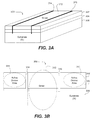
- FIG. 3A is a perspective view of a work piece cut according to another embodiment of the invention.
- FIG. 3B is a side view schematic of the work piece shown in FIG. 3A .
- FIG. 4 graphically illustrates the difference between a simplified Gaussian beam irradiance profile and a simplified shaped beam irradiance profile.
- FIGS. 5A-5C graphically illustrate the difference between beam cross section profiles.
- FIGS. 6A-6D show exemplary substantially uniform irradiance profiles produced by a Gaussian beam propagating through a diffractive optical element (DOE) according to certain embodiments of the invention.
- DOE diffractive optical element
- FIG. 7 is an electron micrograph of a kerf scribed through interconnect and low-k dielectric layers according to an embodiment of the invention.
- FIG. 8 schematically illustrates sequentially exposing a work piece to laser pulses in the direction of a cut according to an embodiment of the invention.
- FIG. 9 is an electron micrograph of a micromachined pattern in a semiconductor material using laser ablation methods according to an embodiment of the invention.
- FIG. 10 is an electron micrograph of a micromachined pattern in a semiconductor material using laser ablation according to an embodiment of the invention.
- the ability of a material to absorb laser energy determines the depth to which that energy can perform ablation.
- Ablation depth is determined by the absorption depth of the material and the heat of vaporization of the material.
- Parameters such as wavelength, pulse width duration, pulse repetition frequency, and beam quality can be controlled to improve cutting speed and the quality of the cut surface or kerf.
- one or more of these parameters are selected so as to provide a substantially low fluence (typically measured in J/cm 2 ) that has just enough energy to ablate the target material.
- a substantially low fluence typically measured in J/cm 2
- Using a lower fluence reduces or eliminates recast oxide layers, heat affected zones, chipping, cracking, and debris. Thus, die break strength is increased and the amount of post-laser cleaning required is decreased.
- the ablation threshold of a material is a function of laser pulse width.
- ablation threshold is a broad term that includes its ordinary and customary meaning, and includes, for example, a sufficient fluence required to remove material for scribing or cutting.
- Traditional pulse widths in the nanosecond range generally require a higher ablation threshold as compared to that of shorter pulse widths. Shorter pulses increase peak power and reduce thermal conduction.
- the Mourou et al. patent teaches using pulse widths in the femtosecond range. However, femtosecond laser pulse widths remove smaller amounts of material per pulse as compared to traditional nanosecond pulses. Thus, the amount of time required to cut or scribe a line is increased and throughput is reduced. Further, in the femtosecond pulse range, the ablation threshold may increase as the femtosecond pulses become shorter.
- pulse widths are selected in the picosecond range to lower the ablation threshold while removing more material per pulse than femtosecond pulses.
- the time constant for electrons initially excited by the laser pulse to exchange energy with the bulk of material e.g., electron thermalization with consecutive electron-lattice interaction
- the time constant may be on the order of approximately 1 to 10 picoseconds.
- pulses in the range between approximately 1 picosecond and approximately 10 picoseconds may provide some thermal type ablation.
- using relatively low fluence per pulse that is only slightly above the ablation threshold reduces excessive energy that produces melted debris. Thus, cleaner kerfs are produced.
- the heat effects are generally limited to the laser spot because the pulse widths are too short for heat to diffuse or propagate outside the irradiated area.
- the effective depth of the laser light interaction with the material is shortened and the efficiency of the ablation is reduced (e.g., less electrons are initially excited by the laser pulse).
- the pulse repetition frequency is selected so as to provide cutting speeds of conventional saw or laser semiconductor cutting processes. High pulse repetition frequencies are used to ablate material quicker. Further, high pulse repetition frequencies allow more energy to be used for ablation before it is dissipated in the surrounding materials.
- beam shaping is used in certain embodiments to improve kerf quality.
- Laser beams can be shaped to create, for example, a substantially flat kerf bottom that generates less debris and reduces or eliminates damage to the substrate.
- beam shaping also reduces the width of the recast oxide layer.
- cutting may be used generically to include scribing (cutting that does not penetrate the full depth of a target work piece) and throughcutting, which includes slicing (often associated with wafer row separation) or dicing (often associated with part singulation from wafer rows). Slicing and dicing may be used interchangeably in the context of this disclosure.
- FIGS. 2A-2C are side view schematics of an exemplary work piece 200 that is cut according to certain embodiments of the invention.
- the work piece 200 includes layers 202 , 204 , 206 formed over a substrate 208 .
- the layers 202 , 204 , 206 may include interconnect layers separated by insulation layers, including low-k dielectrics, to form electronic circuitry.
- the layers 202 , 204 , 206 may include materials such as Cu, Al, SiO 2 , SiN, fluorsilicated glass (FSG), organosilicated glass (OSG), SiOC, SiOCN, and other materials used in IC manufacture.
- the substrate 208 comprises Si.
- other materials useful in IC manufacture can be used for the substrate 208 including, for example, glasses, polymers, metals, composites, and other materials.
- the substrate 208 may include FR4.
- Electronic circuitry is formed in active device areas 210 , 212 that are separated from each other by scribing lanes or streets 214 .
- An artisan will recognize that test structures are often formed in and around the streets 214 .
- the work piece 200 is scribed, throughcut, or both, along the streets 214 .
- a laser beam 216 according to one embodiment is shown scribing the work piece 200 by ablating the layers 202 , 204 , 206 in the area of the street 214 . As shown in FIG.
- the result of the laser scribing process is a laser kerf 218 that passes from the top surface of the top layer 202 through the layers 202 , 204 , 206 to the top surface of the substrate 208 .
- the laser beam 216 is shaped so as to increase the quality of the kerf's sidewall profile and reduce or prevent damage to the substrate 208 .
- the laser beam 216 comprises a series of laser pulses configured to provide the lowest possible fluence to the work piece 200 that still provides a desired material ablation of the layers 202 , 204 , 206 and/or the substrate 208 .
- the fluence of the laser beam 216 is selected so as to be in a range between the ablation threshold of the work piece 200 and approximately ten times the ablation threshold of the work piece 200 .
- the fluence of the laser beam 216 is selected so as to be in a range between the ablation threshold of the work piece 200 and approximately five times the ablation threshold of the work piece 200 .
- the pulse width is set in a range between approximately 0.1 picosecond and approximately 1000 picoseconds. In other embodiments, the pulse width is set in a range between approximately 1 picosecond and approximately 10 picoseconds. In other embodiments, the pulse width is set in a range between 10 picoseconds and 40 picoseconds. However, an artisan will recognize from the disclosure herein that other pulse widths can be used. For example, in one embodiment, the pulse width is in a range between approximately 0.6 picosecond and approximately 190 picoseconds, while in another embodiment, the pulse width is in a range between approximately 210 picoseconds and 1000 picoseconds.
- the laser beam 216 is generated using an average power in a range between approximately 10 W and approximately 50 W and an energy per pulse between approximately 1 ⁇ J and approximately 100 ⁇ J.
- the laser beam 216 is configured to cut through the layers 202 , 204 , 206 at a rate in a range between approximately 200 mm/second and approximately 1000 mm/second using high pulse repetition frequencies.
- the separation between pulses is in a range between approximately 1 nanosecond and approximately 10 nanoseconds to allow substantially complete heat dissipation. In other embodiments, the separation between pulses is in a range between approximately 10 nanoseconds and approximately 1 microseconds to allow the plume of ablated material in a first pulse to spread to a sufficiently low density so as to not significantly interact with a subsequent pulse.
- the pulse repetition frequency is in a range between approximately 1 MHz and approximately 100 MHz. In other embodiments, the pulse repetition frequency is in a range between approximately 5.1 MHz and approximately 100 MHz. In another embodiment, the pulse repetition frequency is in a range between approximately 50 kHz and approximately 4 MHz.
- the laser beam 216 is generated using a DuettoTM laser available from Time-Bandwidth Products of Zurich, Switzerland.
- the DuettoTM laser has a wavelength of approximately 1064 nm, a pulse repetition frequency in a range between approximately 50 kHz and approximately 4 MHz, an average power of approximately 10 W or more, a peak power of up to approximately 16 MW, an energy per pulse of up to approximately 200 ⁇ J, and a pulse width of up to approximately 12 picoseconds.
- the laser beam 216 is generated using a “RAPID” picosecond laser available from Lumera-Laser GmbH of Kaiserslautern, Germany.
- Harmonics of the 1064 nm laser can also be used to improve ablation for specific materials.
- a wavelength of approximately 532 nm can be used to ablate Cu
- a wavelength of approximately 355 nm can be used to ablate Si and certain low-k dielectrics
- a wavelength of approximately 266 nm can be used to ablate glass.
- the wavelength is selected based at least in part on the respective materials and relative thicknesses of the layers 202 , 204 , 206 and/or the substrate 208 so as to increase cutting speed.
- the wavelength may be optimized to ablate a thick Cu layer rather than a relatively thin dielectric layer.
- the wavelength may be changed between ablation of one or more of the layers 202 , 204 , 206 , and/or the substrate 208 .
- An artisan will also recognize that using the harmonics will also improve the ability to focus the laser beam because focusing is dependent on wavelength.
- the fluence of each laser pulse is set at or above the highest ablation threshold in the stack of layers 202 , 204 , 206 for a given wavelength, pulse energy, and pulse duration. In one embodiment, the fluence of each laser pulse is set in a range between approximately one and ten times the highest ablation threshold in the stack. In another embodiment, the fluence of each laser pulse is set in a range between approximately one and five times the highest ablation threshold in the stack.
- the third layer 206 has a higher ablation threshold than the first and second layers 202 , 204 .
- setting the fluence of the laser pulses so as to ablate the third layer 206 also provides ablation of the first and second layers 202 , 204 .
- the fluence is set at approximately 1.5 times the highest ablation threshold in the stack.
- the laser beam 216 is configured to generate approximately 20 ⁇ J pulses with a spot size of approximately 10 ⁇ m to achieve a fluence in a range between approximately 15 ⁇ J/cm 2 and approximately 20 ⁇ J/cm 2 .
- the laser beam 216 may be configured to ablate the top two layers 202 , 204 without ablating the third layer 206 .
- the laser beam 214 may be configured to cut through the layers 202 , 204 , 206 and the substrate 208 to fully separate the active device areas 210 , 212 from one another (e.g., dicing).
- silicon substrates having a thickness in a range between approximately 10 ⁇ m and approximately 760 ⁇ m are throughcut using a laser cutting process. Artisans will recognize from the disclosure herein that other substrate thicknesses can also be throughcut according to the methods described herein.
- the work piece 200 is scribed to remove at least a portion of the layers 202 , 204 , 206 in the street 214 .
- the work piece 200 can then be mechanically broken or mechanically sawed along the kerf path 218 to complete the dicing process.
- materials that may be damaged by the saw and/or that can damage the saw, such as low-k dielectrics or test structures, can be removed before sawing.
- the saw follows the kerf 218 so as to not touch the layers 202 , 204 , 206 .
- cracking and debris are reduced, die break strength is increased and overall yield is improved.
- FIG. 3A is a perspective view of a work piece 300 cut according to another embodiment of the invention.
- the work piece 300 includes layers 302 , 304 formed over a substrate 306 .
- the layers 302 , 304 may include, for example, materials such as Cu, Al, SiO 2 , SiN, fluorsilicated glass (FSG), organosilicated glass (OSG), SiOC, SiOCN, and other materials used in IC manufacture.
- the substrate 306 may include, for example, Si, FR4, glass, polymer, metal, composite material, and other materials used in IC manufacture.
- FIG. 3B is a side view schematic of the work piece 300 shown in FIG. 3A .
- electronic circuitry is formed in active device areas 308 , 310 that are separated from each other by a street 312 .
- the work piece 300 is scribed such that laser kerfs 314 , 316 are formed using laser parameters described herein on both sides of the street 312 .
- the laser kerfs 314 , 316 are each in a range between approximately 5 ⁇ m and approximately 10 ⁇ m wide.
- the laser kerfs 308 , 310 extend into the substrate 306 .
- the laser kerfs 308 , 310 remove material only in one or both of the layers 302 , 304 .
- the laser scribes 314 , 316 act as “crack stops” or physical barriers for heat and mechanical stress during further processing.
- the laser scribes 314 , 316 provide mechanical separation and thermal separation between the street 312 and the active device areas 308 , 310 .
- the street 312 can be mechanically sawed to dice the active device areas 308 , 310 .
- the harsh effects of sawing the street 312 do not propagate to the active device areas 308 , 310 such that cracking and chipping associated with mechanical sawing is reduced or eliminated in these areas.
- the laser beam 216 shown in FIG. 2A is shaped so as to increase the quality of the kerf's sidewall profile and reduce or prevent damage to the substrate 208 .
- FIG. 4 graphically illustrates the difference between a simplified Gaussian beam irradiance profile 402 and a simplified shaped beam irradiance profile 404 .
- the center of the Gaussian beam irradiance profile 402 is much larger than the vaporization threshold 406 and the melting threshold 408 as compared to the shaped beam irradiance profile 404 .
- the Gaussian beam puts a larger amount of excessive energy into the target material, especially at the center of the beam.
- the slope of the Gaussian beam irradiance profile 402 between the melting threshold 408 and the vaporization threshold is less than that of the shaped beam irradiance profile 404 .
- the Gaussian beam will produce a wider recast oxide layer because a wider area of material will be melted but not vaporized.
- the arrows 410 represent the width of the recast oxide layer produced by the Gaussian beam while the arrows 412 represent the width of the recast oxide layer produced by the shaped beam. Due to the rapid slope of the shaped beam irradiance profile 404 between the melting threshold 408 and the vaporization threshold 406 , the shaped beam produces a narrower recast oxide layer.
- FIGS. 5A-5C graphically illustrate the difference between beam cross section profiles.
- FIG. 5A shows a Gaussian cross section profile 510 .
- FIGS. 5B-5C show “top hat” shaped cross section profiles.
- FIG. 5B shows a square cross section profile 512 and
- FIG. 5C shows a round cross section profile 514 .
- FIGS. 6A-6D show exemplary substantially uniform irradiance profiles produced by a Gaussian beam propagating through a diffractive optical element (DOE) as described in U.S. Pat. No. 5,864,430.
- DOE diffractive optical element
- FIGS. 6A-6D show “top hat” shaped beams.
- FIGS. 6A-6C show square irradiance profiles, and FIG. 6D shows a cylindrical irradiance profile.
- the irradiance profile of FIG. 6C is “inverted,” showing higher intensity at its edges than toward its center.
- Beam shaping components can be selected to produce pulses having an inverted irradiance profile shown in FIG. 6C that is clipped outside dashed lines 610 to facilitate ablation to further improve kerf taper.
- beam shaping components can be designed to supply a variety of other irradiance profiles that might be useful for specific applications.
- FIG. 7 is an electron micrograph of a kerf 700 scribed through interconnect and low-k dielectric layers 702 .
- the kerf 700 is approximately 35 ⁇ m wide and was scribed using a laser having a wavelength of approximately 355 nm.
- a short pulse width e.g., in the picosecond range
- a rapid pulse rate frequency were used to achieve low fluence ablation at high speeds.
- the kerf 700 was scribed at a speed of over 500 mm/s with a “top hat” shaped beam.
- the beam shaping provides a kerf bottom that is substantially flat and sides that are substantially vertical and well defined. Further, there is substantially no chipping or cracking.
- scribing can be accomplished using a single laser pass.
- the amount of material removed per pulse is not sufficient to achieve the desired scribe depth in one laser pass.
- each location in the scribe line is exposed with multiple pulses to achieve desired material removal.
- material is exposed with pulses overlapping in the direction of a cut.
- FIG. 8 schematically illustrates sequentially exposing a work piece 800 to laser pulses in the direction of a cut.
- Each pulse ablates a certain spot size 802 to a pulse ablation depth.
- sequential pulses have an overlap offset or bite size 804 in the direction of the cut.
- a first pulse removes material in a first area 806 .
- a second pulse shifted in the direction of the cut removes additional material from a second area 808 and a third area 808 ′.
- the width of the second area 808 and the third area 808 ′ (when combined) is the same as the width of the first area 806 (e.g., the spot size 802 ).
- the second area 808 is to the side of the first area 806 in the direction of the cut and has a width equal to the bite size 804 .
- the third area 808 ′ is below a portion of the first area 806 .
- the overall ablation depth increases from the first pulse to the second pulse.
- the scribing process continues as additional pulses are sequentially applied to the work piece 800 in the direction of the cut.
- the overall depth of the cut increases with each pulse until a desired depth 810 is reached.
- additional pulses continue to remove material in the direction of the cut without increasing the overall depth past the desired depth 810 .
- the bite size 804 will define the desired depth 810 .
- the desired depth 810 is equal to the pulse ablation depth of a single pulse multiplied by the ratio of the spot size 802 to the bite size 804 .
- the bite size 804 is approximately one-seventh the size of the spot size 802 .
- the desired depth 810 is seven times the pulse ablation depth of a single pulse (and is first reached after seven pulses).
- the cut speed is controlled by first selecting the pulse duration as discussed above to reduce the threshold of ablation.
- a pulse width is selected that provides substantially the lowest ablation threshold for the target material or materials.
- the spot size is selected to provide the desired fluence for a selected energy per pulse.
- the bite size is then selected to provide the overall ablation depth.
- the pulse repetition frequency is then selected to increase cut speed.
- lower pulse repetition frequencies e.g., approximately 70 kHz
- high pulse energies e.g., approximately 50 ⁇ J to approximately 100 ⁇ J
- asymmetrical e.g., elliptical or rectangular
- an elliptical or rectangular spot spreads the energy of each pulse to lower the fluence while removing material in the direction of the cut.
- a shaped rectangular beam may be configured such that the longer dimension of the rectangle is in the direction of the cut.
- FIG. 9 is an electron micrograph of a micromachined pattern 900 in a semiconductor material using the laser ablation methods described above.
- the exemplary pattern 900 includes trenches 902 approximately 51 ⁇ m wide cut in a precise pattern.
- the trenches 902 have substantially flat bottoms and well defined side walls. Further, the distance 904 between trenches is as small as approximately 25 ⁇ m.
- FIG. 10 is an electron micrograph of a micromachined pattern 1000 in a semiconductor material using the laser ablation methods described above.
- the exemplary pattern 1000 includes trenches 1002 approximately 50 ⁇ m wide that are separated in some locations 1004 by distances approximately 10 ⁇ m wide.
- FIGS. 7 , 8 and 9 it can be observed that there is substantially no chipping, cracking or contamination.
- some cleaning may be desired to remove small amounts of debris.
- conventional high pressure water or solid CO 2 “sand blasting” techniques can be used after laser ablation to remove particles or debris.
- the ablation processes discussed herein are generally cleaner than conventional laser or mechanical saw cutting techniques and require less cleaning than conventional processes or no cleaning at all. Thus, additional lateral separation between devices on a wafer is not required to accommodate the dicing process.
- due to the low fluence used with short wavelengths there are less problems with heat affected zones, cracking, peeling, and chipping. Thus, higher die break strengths and overall process yields are achieved.
Abstract
Description
Claims (19)
Priority Applications (1)
| Application Number | Priority Date | Filing Date | Title |
|---|---|---|---|
| US14/098,229 US9221124B2 (en) | 2006-05-25 | 2013-12-05 | Ultrashort laser pulse wafer scribing |
Applications Claiming Priority (2)
| Application Number | Priority Date | Filing Date | Title |
|---|---|---|---|
| US11/440,792 US8624157B2 (en) | 2006-05-25 | 2006-05-25 | Ultrashort laser pulse wafer scribing |
| US14/098,229 US9221124B2 (en) | 2006-05-25 | 2013-12-05 | Ultrashort laser pulse wafer scribing |
Related Parent Applications (1)
| Application Number | Title | Priority Date | Filing Date |
|---|---|---|---|
| US11/440,792 Continuation US8624157B2 (en) | 2006-05-25 | 2006-05-25 | Ultrashort laser pulse wafer scribing |
Publications (2)
| Publication Number | Publication Date |
|---|---|
| US20140091069A1 US20140091069A1 (en) | 2014-04-03 |
| US9221124B2 true US9221124B2 (en) | 2015-12-29 |
Family
ID=38748591
Family Applications (2)
| Application Number | Title | Priority Date | Filing Date |
|---|---|---|---|
| US11/440,792 Expired - Fee Related US8624157B2 (en) | 2006-05-25 | 2006-05-25 | Ultrashort laser pulse wafer scribing |
| US14/098,229 Expired - Fee Related US9221124B2 (en) | 2006-05-25 | 2013-12-05 | Ultrashort laser pulse wafer scribing |
Family Applications Before (1)
| Application Number | Title | Priority Date | Filing Date |
|---|---|---|---|
| US11/440,792 Expired - Fee Related US8624157B2 (en) | 2006-05-25 | 2006-05-25 | Ultrashort laser pulse wafer scribing |
Country Status (8)
| Country | Link |
|---|---|
| US (2) | US8624157B2 (en) |
| JP (1) | JP2009538231A (en) |
| KR (1) | KR101385675B1 (en) |
| CN (1) | CN101490819B (en) |
| DE (1) | DE112007001280T5 (en) |
| GB (1) | GB2452430A (en) |
| TW (1) | TWI428970B (en) |
| WO (1) | WO2007140149A1 (en) |
Cited By (2)
| Publication number | Priority date | Publication date | Assignee | Title |
|---|---|---|---|---|
| US10586654B2 (en) | 2017-12-21 | 2020-03-10 | General Atomics | Glass dielectric capacitors and manufacturing processes for glass dielectric capacitors |
| US11072109B2 (en) | 2013-09-20 | 2021-07-27 | Essilor International | Device and process for marking an ophthalmic lens with a pulsed laser of wavelength and energy selected per pulse |
Families Citing this family (78)
| Publication number | Priority date | Publication date | Assignee | Title |
|---|---|---|---|---|
| US20070272666A1 (en) * | 2006-05-25 | 2007-11-29 | O'brien James N | Infrared laser wafer scribing using short pulses |
| US8624157B2 (en) | 2006-05-25 | 2014-01-07 | Electro Scientific Industries, Inc. | Ultrashort laser pulse wafer scribing |
| SG138540A1 (en) * | 2006-06-08 | 2008-01-28 | Apic Yamada Corp | Semiconductor cutting device, semiconductor cutting method, semiconductor cutting system, laser cutting device and laser cutting method |
| JP2009142832A (en) * | 2007-12-12 | 2009-07-02 | Disco Abrasive Syst Ltd | Laser beam machining apparatus |
| CN105583526B (en) | 2008-03-21 | 2018-08-17 | Imra美国公司 | Material processing method based on laser and system |
| GB2459669A (en) * | 2008-04-30 | 2009-11-04 | Xsil Technology Ltd | Dielectric layer pulsed laser scribing and metal layer and semiconductor wafer dicing |
| JP2012504350A (en) * | 2008-09-29 | 2012-02-16 | シンシリコン・コーポレーション | Integrated solar module |
| JP2010114190A (en) * | 2008-11-05 | 2010-05-20 | Mitsubishi Heavy Ind Ltd | Method of manufacturing photoelectric conversion device, and photoelectric conversion device |
| US8309885B2 (en) * | 2009-01-15 | 2012-11-13 | Electro Scientific Industries, Inc. | Pulse temporal programmable ultrafast burst mode laser for micromachining |
| JP5328406B2 (en) * | 2009-02-19 | 2013-10-30 | 株式会社日立ハイテクノロジーズ | Laser processing method, laser processing apparatus, and solar panel manufacturing method |
| JP2010188396A (en) * | 2009-02-19 | 2010-09-02 | Hitachi High-Technologies Corp | Laser beam machining method, laser beam machining device, and method for producing solar panel |
| US8609512B2 (en) * | 2009-03-27 | 2013-12-17 | Electro Scientific Industries, Inc. | Method for laser singulation of chip scale packages on glass substrates |
| US8729427B2 (en) | 2009-03-27 | 2014-05-20 | Electro Scientific Industries, Inc. | Minimizing thermal effect during material removal using a laser |
| US10307862B2 (en) * | 2009-03-27 | 2019-06-04 | Electro Scientific Industries, Inc | Laser micromachining with tailored bursts of short laser pulses |
| JP2010251428A (en) * | 2009-04-13 | 2010-11-04 | Mitsubishi Heavy Ind Ltd | Photoelectric conversion device manufacturing method, photoelectric conversion device manufacturing device, and photoelectric conversion device |
| JP5473414B2 (en) * | 2009-06-10 | 2014-04-16 | 株式会社ディスコ | Laser processing equipment |
| US9044829B2 (en) * | 2009-11-09 | 2015-06-02 | Nlight Photonics Corporation | Fiber laser systems for cold ablation |
| US20130256286A1 (en) * | 2009-12-07 | 2013-10-03 | Ipg Microsystems Llc | Laser processing using an astigmatic elongated beam spot and using ultrashort pulses and/or longer wavelengths |
| CN102639280A (en) * | 2009-12-07 | 2012-08-15 | Jp赛席尔联合股份有限公司 | Laser machining and scribing systems and methods |
| JP2011161491A (en) * | 2010-02-10 | 2011-08-25 | Disco Abrasive Syst Ltd | Laser beam machining apparatus |
| JP5693705B2 (en) | 2010-03-30 | 2015-04-01 | イムラ アメリカ インコーポレイテッド | Laser-based material processing apparatus and method |
| US8383984B2 (en) * | 2010-04-02 | 2013-02-26 | Electro Scientific Industries, Inc. | Method and apparatus for laser singulation of brittle materials |
| US8389895B2 (en) * | 2010-06-25 | 2013-03-05 | Electro Scientifix Industries, Inc. | Method and apparatus for reliably laser marking articles |
| US20120074109A1 (en) * | 2010-09-29 | 2012-03-29 | General Electric Company | Method and system for scribing a multilayer panel |
| US8048778B1 (en) * | 2010-12-10 | 2011-11-01 | Taiwan Semiconductor Manufacturing Company, Ltd. | Methods of dicing a semiconductor structure |
| US8411716B2 (en) | 2011-01-26 | 2013-04-02 | Institut National D'optique | Circuit assembly for controlling an optical system to generate optical pulses and pulse bursts |
| US8735772B2 (en) * | 2011-02-20 | 2014-05-27 | Electro Scientific Industries, Inc. | Method and apparatus for improved laser scribing of opto-electric devices |
| US8648277B2 (en) | 2011-03-31 | 2014-02-11 | Electro Scientific Industries, Inc. | Laser direct ablation with picosecond laser pulses at high pulse repetition frequencies |
| US8557683B2 (en) * | 2011-06-15 | 2013-10-15 | Applied Materials, Inc. | Multi-step and asymmetrically shaped laser beam scribing |
| US9129904B2 (en) * | 2011-06-15 | 2015-09-08 | Applied Materials, Inc. | Wafer dicing using pulse train laser with multiple-pulse bursts and plasma etch |
| US8361828B1 (en) | 2011-08-31 | 2013-01-29 | Alta Devices, Inc. | Aligned frontside backside laser dicing of semiconductor films |
| US8399281B1 (en) | 2011-08-31 | 2013-03-19 | Alta Devices, Inc. | Two beam backside laser dicing of semiconductor films |
| US8728849B1 (en) | 2011-08-31 | 2014-05-20 | Alta Devices, Inc. | Laser cutting through two dissimilar materials separated by a metal foil |
| US8728933B1 (en) | 2011-08-31 | 2014-05-20 | Alta Devices, Inc. | Laser cutting and chemical edge clean for thin-film solar cells |
| US10357850B2 (en) | 2012-09-24 | 2019-07-23 | Electro Scientific Industries, Inc. | Method and apparatus for machining a workpiece |
| US9828278B2 (en) | 2012-02-28 | 2017-11-28 | Electro Scientific Industries, Inc. | Method and apparatus for separation of strengthened glass and articles produced thereby |
| US9828277B2 (en) * | 2012-02-28 | 2017-11-28 | Electro Scientific Industries, Inc. | Methods for separation of strengthened glass |
| WO2013130608A1 (en) | 2012-02-29 | 2013-09-06 | Electro Scientific Industries, Inc. | Methods and apparatus for machining strengthened glass and articles produced thereby |
| JP2013197428A (en) * | 2012-03-22 | 2013-09-30 | Aisin Seiki Co Ltd | Thin-film semiconductor element and method for manufacturing the same |
| WO2013156891A1 (en) * | 2012-04-16 | 2013-10-24 | Koninklijke Philips N.V. | Method and apparatus for creating a w-mesa street |
| JP6000700B2 (en) * | 2012-07-10 | 2016-10-05 | 株式会社ディスコ | Laser processing method |
| EP2762286B1 (en) | 2013-01-31 | 2015-07-01 | ams AG | Dicing method |
| GB2514084B (en) * | 2013-02-21 | 2016-07-27 | M-Solv Ltd | Method of forming an electrode structure for capacitive touch sensor |
| WO2014134470A1 (en) * | 2013-02-28 | 2014-09-04 | Ipg Photonics Corporation | Laser system and method for processing sapphire |
| US10286487B2 (en) * | 2013-02-28 | 2019-05-14 | Ipg Photonics Corporation | Laser system and method for processing sapphire |
| US9102011B2 (en) | 2013-08-02 | 2015-08-11 | Rofin-Sinar Technologies Inc. | Method and apparatus for non-ablative, photoacoustic compression machining in transparent materials using filamentation by burst ultrafast laser pulses |
| US9517929B2 (en) | 2013-11-19 | 2016-12-13 | Rofin-Sinar Technologies Inc. | Method of fabricating electromechanical microchips with a burst ultrafast laser pulses |
| US10005152B2 (en) | 2013-11-19 | 2018-06-26 | Rofin-Sinar Technologies Llc | Method and apparatus for spiral cutting a glass tube using filamentation by burst ultrafast laser pulses |
| US10252507B2 (en) | 2013-11-19 | 2019-04-09 | Rofin-Sinar Technologies Llc | Method and apparatus for forward deposition of material onto a substrate using burst ultrafast laser pulse energy |
| US11053156B2 (en) | 2013-11-19 | 2021-07-06 | Rofin-Sinar Technologies Llc | Method of closed form release for brittle materials using burst ultrafast laser pulses |
| US10144088B2 (en) | 2013-12-03 | 2018-12-04 | Rofin-Sinar Technologies Llc | Method and apparatus for laser processing of silicon by filamentation of burst ultrafast laser pulses |
| US9938187B2 (en) | 2014-02-28 | 2018-04-10 | Rofin-Sinar Technologies Llc | Method and apparatus for material processing using multiple filamentation of burst ultrafast laser pulses |
| US10343237B2 (en) | 2014-02-28 | 2019-07-09 | Ipg Photonics Corporation | System and method for laser beveling and/or polishing |
| US9764427B2 (en) | 2014-02-28 | 2017-09-19 | Ipg Photonics Corporation | Multi-laser system and method for cutting and post-cut processing hard dielectric materials |
| US9956646B2 (en) | 2014-02-28 | 2018-05-01 | Ipg Photonics Corporation | Multiple-beam laser processing using multiple laser beams with distinct wavelengths and/or pulse durations |
| JP2015170675A (en) * | 2014-03-06 | 2015-09-28 | 株式会社ディスコ | Processing method of plate-like object |
| WO2015175268A1 (en) * | 2014-05-16 | 2015-11-19 | Applied Materials, Inc. | Hybrid wafer dicing approach using an ultra-short pulsed laguerre gauss beam laser scribing process and plasma etch process |
| US20150360326A1 (en) * | 2014-06-12 | 2015-12-17 | Siemens Energy, Inc. | Method to eliminate recast material |
| US9093518B1 (en) * | 2014-06-30 | 2015-07-28 | Applied Materials, Inc. | Singulation of wafers having wafer-level underfill |
| US9165832B1 (en) | 2014-06-30 | 2015-10-20 | Applied Materials, Inc. | Method of die singulation using laser ablation and induction of internal defects with a laser |
| LT2965853T (en) * | 2014-07-09 | 2016-11-25 | High Q Laser Gmbh | Processing of material using elongated laser beams |
| US9757815B2 (en) | 2014-07-21 | 2017-09-12 | Rofin-Sinar Technologies Inc. | Method and apparatus for performing laser curved filamentation within transparent materials |
| WO2016033494A1 (en) | 2014-08-28 | 2016-03-03 | Ipg Photonics Corporation | System and method for laser beveling and/or polishing |
| CN114603249A (en) | 2014-08-28 | 2022-06-10 | Ipg光子公司 | Multi-laser system and method for cutting and post-cutting machining of hard dielectric materials |
| CN106132627B (en) | 2015-01-13 | 2018-09-07 | 罗芬-新纳技术有限责任公司 | For carrying out scribing and the then method and system of progress chemical etching to fragile material |
| WO2016113948A1 (en) * | 2015-01-13 | 2016-07-21 | コニカミノルタ株式会社 | Method and apparatus for manufacturing electronic device |
| DE202015009023U1 (en) * | 2015-06-19 | 2016-07-18 | Laser- Und Medizin- Technologie Gmbh | Lateral radiating optical fibers |
| JP6666173B2 (en) * | 2016-03-09 | 2020-03-13 | 株式会社ディスコ | Laser processing equipment |
| US10720360B2 (en) * | 2016-07-29 | 2020-07-21 | Taiwan Semiconductor Manufacturing Company, Ltd. | Semiconductor die singulation and structures formed thereby |
| DE102017100349B4 (en) | 2016-07-29 | 2024-04-18 | Taiwan Semiconductor Manufacturing Co., Ltd. | Separation of semiconductor dies and resulting structures |
| JP6467688B2 (en) * | 2017-02-08 | 2019-02-13 | パナソニックIpマネジメント株式会社 | Device chip manufacturing method |
| JP6781649B2 (en) * | 2017-03-13 | 2020-11-04 | 株式会社ディスコ | Laser processing equipment |
| JP6802093B2 (en) * | 2017-03-13 | 2020-12-16 | 株式会社ディスコ | Laser processing method and laser processing equipment |
| GB2572608A (en) * | 2018-04-03 | 2019-10-09 | Ilika Tech Ltd | Laser processing method for thin film structures |
| TW202400349A (en) * | 2018-10-08 | 2024-01-01 | 美商伊雷克托科學工業股份有限公司 | Methods for forming a through-via in a substrate |
| CN111151892B (en) * | 2018-11-08 | 2022-05-20 | 中国科学院西安光学精密机械研究所 | Non-taper laser cutting method |
| CN112264724A (en) * | 2020-10-28 | 2021-01-26 | 北京理工大学重庆创新中心 | Method for processing microporous structure based on Bessel light beam |
| CN114335251B (en) * | 2021-12-31 | 2023-01-20 | 成都中建材光电材料有限公司 | Laser scribing equipment, scribing method of thin-film photovoltaic chip and power generation building board |
Citations (41)
| Publication number | Priority date | Publication date | Assignee | Title |
|---|---|---|---|---|
| WO1995027587A1 (en) | 1994-04-08 | 1995-10-19 | The Regents Of The University Of Michigan | Method for controlling configuration of laser induced breakdown and ablation |
| US5593606A (en) | 1994-07-18 | 1997-01-14 | Electro Scientific Industries, Inc. | Ultraviolet laser system and method for forming vias in multi-layered targets |
| US5632083A (en) | 1993-08-05 | 1997-05-27 | Hitachi Construction Machinery Co., Ltd. | Lead frame fabricating method and lead frame fabricating apparatus |
| US5731047A (en) | 1996-11-08 | 1998-03-24 | W.L. Gore & Associates, Inc. | Multiple frequency processing to improve electrical resistivity of blind micro-vias |
| US5864430A (en) * | 1996-09-10 | 1999-01-26 | Sandia Corporation | Gaussian beam profile shaping apparatus, method therefor and evaluation thereof |
| WO2000030801A1 (en) | 1998-11-23 | 2000-06-02 | Minnesota Mining And Manufacturing Company | Ablated laser feature shape reproduction control |
| WO2000073770A1 (en) | 1999-05-27 | 2000-12-07 | Spectra-Physics Lasers, Inc. | Method and apparatus to detect a flaw in a surface of an article |
| WO2001017001A1 (en) | 1999-08-27 | 2001-03-08 | Jmar Research, Inc. | Method and apparatus for laser ablation of a target material |
| US20010054606A1 (en) | 1999-06-08 | 2001-12-27 | Ilan Weishauss | Laser scribing of wafers |
| US6341029B1 (en) | 1999-04-27 | 2002-01-22 | Gsi Lumonics, Inc. | Method and apparatus for shaping a laser-beam intensity profile by dithering |
| US20020033558A1 (en) | 2000-09-20 | 2002-03-21 | Fahey Kevin P. | UV laser cutting or shape modification of brittle, high melting temperature target materials such as ceramics or glasses |
| US20020063361A1 (en) | 2000-09-20 | 2002-05-30 | Fahey Kevin P. | Laser processing of alumina or metals on or embedded therein |
| JP2002172481A (en) * | 2000-12-04 | 2002-06-18 | Matsuura Machinery Corp | Laser beam machining machine |
| US6420245B1 (en) | 1999-06-08 | 2002-07-16 | Kulicke & Soffa Investments, Inc. | Method for singulating semiconductor wafers |
| US6433301B1 (en) | 1999-05-28 | 2002-08-13 | Electro Scientific Industries, Inc. | Beam shaping and projection imaging with solid state UV Gaussian beam to form vias |
| US20020149136A1 (en) | 2000-09-20 | 2002-10-17 | Baird Brian W. | Ultraviolet laser ablative patterning of microstructures in semiconductors |
| US20020158052A1 (en) * | 2001-03-29 | 2002-10-31 | Ehrmann Jonathan S. | Method and system for processing one or more microstructures of a multi-material device |
| WO2003002289A1 (en) | 2001-06-28 | 2003-01-09 | Electro Scientific Industries, Inc. | Multistep laser processing of wafers supporting surface device layers |
| US6562698B2 (en) | 1999-06-08 | 2003-05-13 | Kulicke & Soffa Investments, Inc. | Dual laser cutting of wafers |
| US20030092267A1 (en) | 2001-02-14 | 2003-05-15 | Avery Dennison Corporation | Method for patterning a multilayered conductor/substrate structure |
| US20030183603A1 (en) | 2001-12-04 | 2003-10-02 | Forsman Andrew C. | Method and apparatus for increasing the material removal rate in laser machining |
| US6676878B2 (en) * | 2001-01-31 | 2004-01-13 | Electro Scientific Industries, Inc. | Laser segmented cutting |
| EP1433195A2 (en) | 2001-10-01 | 2004-06-30 | Xsil Technology Limited | Method of machining substrates |
| US6791060B2 (en) | 1999-05-28 | 2004-09-14 | Electro Scientific Industries, Inc. | Beam shaping and projection imaging with solid state UV gaussian beam to form vias |
| GB2405369A (en) | 2003-09-01 | 2005-03-02 | Toshiba Kk | Apparatus for laser beam machining , machining mask, method for laser beam machining, method for manufacturing a semiconductor and semiconductor device |
| JP2005072174A (en) | 2003-08-22 | 2005-03-17 | Disco Abrasive Syst Ltd | Separation method of workpiece formed by substrate and laminate stacked on its front surface |
| US20050074974A1 (en) * | 2003-10-02 | 2005-04-07 | Richard Stoltz | Semiconductor manufacturing using optical ablation |
| US20050087522A1 (en) * | 2003-10-24 | 2005-04-28 | Yunlong Sun | Laser processing of a locally heated target material |
| WO2005042421A1 (en) | 2003-10-31 | 2005-05-12 | The Japan Steel Works, Ltd. | Glass cutting method |
| TW200520080A (en) | 2003-12-11 | 2005-06-16 | Advanced Semiconductor Eng | Method for dicing a wafer |
| JP2005179154A (en) | 2003-12-22 | 2005-07-07 | Shibuya Kogyo Co Ltd | Method and apparatus for fracturing brittle material |
| US20050155954A1 (en) * | 2004-01-20 | 2005-07-21 | Disco Corporation | Semiconductor wafer processing method |
| US20050155956A1 (en) * | 2002-08-30 | 2005-07-21 | Sumitomo Heavy Industries, Ltd. | Laser processing method and processing device |
| JP2005212473A (en) | 2004-02-02 | 2005-08-11 | Mitsuboshi Diamond Industrial Co Ltd | Scribing apparatus and scribing method employing scribing apparatus |
| EP1589579A2 (en) | 2004-04-22 | 2005-10-26 | Hewlett-Packard Development Company, L.P. | A method for patterning an organic light emitting diode device |
| US20050274702A1 (en) | 2004-06-15 | 2005-12-15 | Laserfacturing Inc. | Method and apparatus for dicing of thin and ultra thin semiconductor wafer using ultrafast pulse laser |
| US20060035411A1 (en) * | 2004-08-11 | 2006-02-16 | Disco Corporation | Laser processing method |
| US20060039419A1 (en) | 2004-08-16 | 2006-02-23 | Tan Deshi | Method and apparatus for laser trimming of resistors using ultrafast laser pulse from ultrafast laser oscillator operating in picosecond and femtosecond pulse widths |
| USRE39001E1 (en) | 2000-01-31 | 2006-03-07 | Electro Scientific Industries, Inc. | Laser cutting method for forming magnetic recording head sliders |
| US20060169677A1 (en) * | 2005-02-03 | 2006-08-03 | Laserfacturing Inc. | Method and apparatus for via drilling and selective material removal using an ultrafast pulse laser |
| US8624157B2 (en) | 2006-05-25 | 2014-01-07 | Electro Scientific Industries, Inc. | Ultrashort laser pulse wafer scribing |
Family Cites Families (2)
| Publication number | Priority date | Publication date | Assignee | Title |
|---|---|---|---|---|
| JP2005279698A (en) * | 2004-03-29 | 2005-10-13 | Nitto Denko Corp | Method of producing laser-processed product and adhesive sheet for laser processing used therefor |
| US7202141B2 (en) * | 2004-03-29 | 2007-04-10 | J.P. Sercel Associates, Inc. | Method of separating layers of material |
-
2006
- 2006-05-25 US US11/440,792 patent/US8624157B2/en not_active Expired - Fee Related
-
2007
- 2007-05-18 JP JP2009512234A patent/JP2009538231A/en active Pending
- 2007-05-18 WO PCT/US2007/069273 patent/WO2007140149A1/en active Application Filing
- 2007-05-18 DE DE112007001280T patent/DE112007001280T5/en not_active Withdrawn
- 2007-05-18 CN CN2007800267542A patent/CN101490819B/en not_active Expired - Fee Related
- 2007-05-18 KR KR1020087028716A patent/KR101385675B1/en active IP Right Grant
- 2007-05-22 TW TW096118204A patent/TWI428970B/en not_active IP Right Cessation
-
2008
- 2008-11-24 GB GB0821328A patent/GB2452430A/en not_active Withdrawn
-
2013
- 2013-12-05 US US14/098,229 patent/US9221124B2/en not_active Expired - Fee Related
Patent Citations (52)
| Publication number | Priority date | Publication date | Assignee | Title |
|---|---|---|---|---|
| US5632083A (en) | 1993-08-05 | 1997-05-27 | Hitachi Construction Machinery Co., Ltd. | Lead frame fabricating method and lead frame fabricating apparatus |
| WO1995027587A1 (en) | 1994-04-08 | 1995-10-19 | The Regents Of The University Of Michigan | Method for controlling configuration of laser induced breakdown and ablation |
| US5656186A (en) | 1994-04-08 | 1997-08-12 | The Regents Of The University Of Michigan | Method for controlling configuration of laser induced breakdown and ablation |
| JP2002205179A (en) | 1994-04-08 | 2002-07-23 | Regents Of The Univ Of Michigan | Method for controlling laser-induced break and cut form |
| US5593606A (en) | 1994-07-18 | 1997-01-14 | Electro Scientific Industries, Inc. | Ultraviolet laser system and method for forming vias in multi-layered targets |
| US5864430A (en) * | 1996-09-10 | 1999-01-26 | Sandia Corporation | Gaussian beam profile shaping apparatus, method therefor and evaluation thereof |
| US5731047A (en) | 1996-11-08 | 1998-03-24 | W.L. Gore & Associates, Inc. | Multiple frequency processing to improve electrical resistivity of blind micro-vias |
| WO2000030801A1 (en) | 1998-11-23 | 2000-06-02 | Minnesota Mining And Manufacturing Company | Ablated laser feature shape reproduction control |
| JP2002530206A (en) | 1998-11-23 | 2002-09-17 | ミネソタ マイニング アンド マニュファクチャリング カンパニー | Reproduction control of feature shape by laser ablation |
| US6341029B1 (en) | 1999-04-27 | 2002-01-22 | Gsi Lumonics, Inc. | Method and apparatus for shaping a laser-beam intensity profile by dithering |
| WO2000073770A1 (en) | 1999-05-27 | 2000-12-07 | Spectra-Physics Lasers, Inc. | Method and apparatus to detect a flaw in a surface of an article |
| US6791060B2 (en) | 1999-05-28 | 2004-09-14 | Electro Scientific Industries, Inc. | Beam shaping and projection imaging with solid state UV gaussian beam to form vias |
| US6433301B1 (en) | 1999-05-28 | 2002-08-13 | Electro Scientific Industries, Inc. | Beam shaping and projection imaging with solid state UV Gaussian beam to form vias |
| US6420245B1 (en) | 1999-06-08 | 2002-07-16 | Kulicke & Soffa Investments, Inc. | Method for singulating semiconductor wafers |
| US20010054606A1 (en) | 1999-06-08 | 2001-12-27 | Ilan Weishauss | Laser scribing of wafers |
| US6562698B2 (en) | 1999-06-08 | 2003-05-13 | Kulicke & Soffa Investments, Inc. | Dual laser cutting of wafers |
| US6555447B2 (en) | 1999-06-08 | 2003-04-29 | Kulicke & Soffa Investments, Inc. | Method for laser scribing of wafers |
| US6472295B1 (en) | 1999-08-27 | 2002-10-29 | Jmar Research, Inc. | Method and apparatus for laser ablation of a target material |
| WO2001017001A1 (en) | 1999-08-27 | 2001-03-08 | Jmar Research, Inc. | Method and apparatus for laser ablation of a target material |
| USRE39001E1 (en) | 2000-01-31 | 2006-03-07 | Electro Scientific Industries, Inc. | Laser cutting method for forming magnetic recording head sliders |
| US20020149136A1 (en) | 2000-09-20 | 2002-10-17 | Baird Brian W. | Ultraviolet laser ablative patterning of microstructures in semiconductors |
| US20020033558A1 (en) | 2000-09-20 | 2002-03-21 | Fahey Kevin P. | UV laser cutting or shape modification of brittle, high melting temperature target materials such as ceramics or glasses |
| US20020063361A1 (en) | 2000-09-20 | 2002-05-30 | Fahey Kevin P. | Laser processing of alumina or metals on or embedded therein |
| JP2002172481A (en) * | 2000-12-04 | 2002-06-18 | Matsuura Machinery Corp | Laser beam machining machine |
| US6676878B2 (en) * | 2001-01-31 | 2004-01-13 | Electro Scientific Industries, Inc. | Laser segmented cutting |
| US20030092267A1 (en) | 2001-02-14 | 2003-05-15 | Avery Dennison Corporation | Method for patterning a multilayered conductor/substrate structure |
| US20020158052A1 (en) * | 2001-03-29 | 2002-10-31 | Ehrmann Jonathan S. | Method and system for processing one or more microstructures of a multi-material device |
| US20050017156A1 (en) | 2001-03-29 | 2005-01-27 | Gsi Lumonics Corporation | High-speed, precision, laser-based method and system for processing material of one or more targets within a field |
| WO2003002289A1 (en) | 2001-06-28 | 2003-01-09 | Electro Scientific Industries, Inc. | Multistep laser processing of wafers supporting surface device layers |
| EP1433195A2 (en) | 2001-10-01 | 2004-06-30 | Xsil Technology Limited | Method of machining substrates |
| US20030183603A1 (en) | 2001-12-04 | 2003-10-02 | Forsman Andrew C. | Method and apparatus for increasing the material removal rate in laser machining |
| US6664498B2 (en) | 2001-12-04 | 2003-12-16 | General Atomics | Method and apparatus for increasing the material removal rate in laser machining |
| US20050155956A1 (en) * | 2002-08-30 | 2005-07-21 | Sumitomo Heavy Industries, Ltd. | Laser processing method and processing device |
| JP2005072174A (en) | 2003-08-22 | 2005-03-17 | Disco Abrasive Syst Ltd | Separation method of workpiece formed by substrate and laminate stacked on its front surface |
| JP2005074485A (en) | 2003-09-01 | 2005-03-24 | Toshiba Corp | Laser beam machining apparatus, working mask, laser beam machining method, method for manufacturing semiconductor device, and semiconductor device |
| GB2405369A (en) | 2003-09-01 | 2005-03-02 | Toshiba Kk | Apparatus for laser beam machining , machining mask, method for laser beam machining, method for manufacturing a semiconductor and semiconductor device |
| US20050074974A1 (en) * | 2003-10-02 | 2005-04-07 | Richard Stoltz | Semiconductor manufacturing using optical ablation |
| US20050087522A1 (en) * | 2003-10-24 | 2005-04-28 | Yunlong Sun | Laser processing of a locally heated target material |
| WO2005042421A1 (en) | 2003-10-31 | 2005-05-12 | The Japan Steel Works, Ltd. | Glass cutting method |
| US7423237B2 (en) | 2003-10-31 | 2008-09-09 | The Japan Steel Works, Ltd. | Method of cutting laminated glass with laser beams |
| TW200520080A (en) | 2003-12-11 | 2005-06-16 | Advanced Semiconductor Eng | Method for dicing a wafer |
| JP2005179154A (en) | 2003-12-22 | 2005-07-07 | Shibuya Kogyo Co Ltd | Method and apparatus for fracturing brittle material |
| US20050155954A1 (en) * | 2004-01-20 | 2005-07-21 | Disco Corporation | Semiconductor wafer processing method |
| JP2005212473A (en) | 2004-02-02 | 2005-08-11 | Mitsuboshi Diamond Industrial Co Ltd | Scribing apparatus and scribing method employing scribing apparatus |
| JP2005310771A (en) | 2004-04-22 | 2005-11-04 | Hewlett-Packard Development Co Lp | Patterning method of organic light emitting diode device |
| EP1589579A2 (en) | 2004-04-22 | 2005-10-26 | Hewlett-Packard Development Company, L.P. | A method for patterning an organic light emitting diode device |
| US20050274702A1 (en) | 2004-06-15 | 2005-12-15 | Laserfacturing Inc. | Method and apparatus for dicing of thin and ultra thin semiconductor wafer using ultrafast pulse laser |
| US20060035411A1 (en) * | 2004-08-11 | 2006-02-16 | Disco Corporation | Laser processing method |
| US20060039419A1 (en) | 2004-08-16 | 2006-02-23 | Tan Deshi | Method and apparatus for laser trimming of resistors using ultrafast laser pulse from ultrafast laser oscillator operating in picosecond and femtosecond pulse widths |
| US20060169677A1 (en) * | 2005-02-03 | 2006-08-03 | Laserfacturing Inc. | Method and apparatus for via drilling and selective material removal using an ultrafast pulse laser |
| US7528342B2 (en) | 2005-02-03 | 2009-05-05 | Laserfacturing, Inc. | Method and apparatus for via drilling and selective material removal using an ultrafast pulse laser |
| US8624157B2 (en) | 2006-05-25 | 2014-01-07 | Electro Scientific Industries, Inc. | Ultrashort laser pulse wafer scribing |
Non-Patent Citations (4)
| Title |
|---|
| Bovastek, James M., et al., "Ultrashort pulse micromaching with the 10-muJ FCPA fiber laser," Fiber Laser III: Technology, Systems, and Applications, Proc. of SP:IE vol. 6102, pp. 610201-1-610201-11, 2006. |
| Bovastek, James M., et al., "Ultrashort pulse micromaching with the 10-μJ FCPA fiber laser," Fiber Laser III: Technology, Systems, and Applications, Proc. of SP:IE vol. 6102, pp. 610201-1-610201-11, 2006. |
| Du, D. et al., "Laser-induced breakdown by impact ionization in SiO2 with pulse widths from 7 ns to 150 fs," Appl. Phys. Lett., vol. 64, No. 23, Jun. 6, 1994, pp. 3071-3073, American Institute of Physics. |
| Ostendorf, A., et al., "Ablation of meals and semiconductors with ultrashort-pulsed lasers: improving surface qualifies of microcuts and grooves," Commercial and Biomedical Applications of Ultrafast Lasers IV, Proc. of SPI vol. 5340, pp. 153-163, Bellingham, Washington, 2004. |
Cited By (2)
| Publication number | Priority date | Publication date | Assignee | Title |
|---|---|---|---|---|
| US11072109B2 (en) | 2013-09-20 | 2021-07-27 | Essilor International | Device and process for marking an ophthalmic lens with a pulsed laser of wavelength and energy selected per pulse |
| US10586654B2 (en) | 2017-12-21 | 2020-03-10 | General Atomics | Glass dielectric capacitors and manufacturing processes for glass dielectric capacitors |
Also Published As
| Publication number | Publication date |
|---|---|
| US20070272668A1 (en) | 2007-11-29 |
| CN101490819B (en) | 2013-06-05 |
| GB0821328D0 (en) | 2008-12-31 |
| GB2452430A (en) | 2009-03-04 |
| US8624157B2 (en) | 2014-01-07 |
| KR101385675B1 (en) | 2014-04-15 |
| JP2009538231A (en) | 2009-11-05 |
| WO2007140149A1 (en) | 2007-12-06 |
| CN101490819A (en) | 2009-07-22 |
| US20140091069A1 (en) | 2014-04-03 |
| TWI428970B (en) | 2014-03-01 |
| TW200809938A (en) | 2008-02-16 |
| KR20090010996A (en) | 2009-01-30 |
| DE112007001280T5 (en) | 2009-04-23 |
Similar Documents
| Publication | Publication Date | Title |
|---|---|---|
| US9221124B2 (en) | Ultrashort laser pulse wafer scribing | |
| US20070272666A1 (en) | Infrared laser wafer scribing using short pulses | |
| US8609512B2 (en) | Method for laser singulation of chip scale packages on glass substrates | |
| KR101754186B1 (en) | Improved method and apparatus for laser singulation of brittle materials | |
| US7611966B2 (en) | Dual pulsed beam laser micromachining method | |
| US8604383B2 (en) | Laser processing method | |
| JP2004343008A (en) | Workpiece dividing method utilizing laser beam | |
| US20060088984A1 (en) | Laser ablation method | |
| EP2283518B1 (en) | Dicing a semiconductor wafer | |
| JP2005019667A (en) | Method for dividing semiconductor wafer by utilizing laser beam | |
| WO2007074823A1 (en) | Laser beam machining method and semiconductor chip | |
| WO2003002289A1 (en) | Multistep laser processing of wafers supporting surface device layers | |
| JP2011508670A (en) | System and method for link processing with ultrafast laser pulses and nanosecond laser pulses | |
| CN215266256U (en) | Semiconductor product | |
| WO2024077749A1 (en) | Laser cutting apparatus and wafer cutting method |
Legal Events
| Date | Code | Title | Description |
|---|---|---|---|
| AS | Assignment |
Owner name: ELECTRO SCIENTIFIC INDUSTRIES, INC., OREGON Free format text: ASSIGNMENT OF ASSIGNORS INTEREST;ASSIGNORS:ALBELO, JEFFREY A.;PIROGOVSKY, PETER;SIGNING DATES FROM 20060809 TO 20060810;REEL/FRAME:031726/0134 |
|
| STCF | Information on status: patent grant |
Free format text: PATENTED CASE |
|
| AS | Assignment |
Owner name: BARCLAYS BANK PLC, AS COLLATERAL AGENT, NEW YORK Free format text: PATENT SECURITY AGREEMENT (TERM LOAN);ASSIGNORS:ELECTRO SCIENTIFIC INDUSTRIES, INC.;MKS INSTRUMENTS, INC.;NEWPORT CORPORATION;REEL/FRAME:048211/0227 Effective date: 20190201 Owner name: BARCLAYS BANK PLC, AS COLLATERAL AGENT, NEW YORK Free format text: PATENT SECURITY AGREEMENT (ABL);ASSIGNORS:ELECTRO SCIENTIFIC INDUSTRIES, INC.;MKS INSTRUMENTS, INC.;NEWPORT CORPORATION;REEL/FRAME:048211/0312 Effective date: 20190201 |
|
| MAFP | Maintenance fee payment |
Free format text: PAYMENT OF MAINTENANCE FEE, 4TH YEAR, LARGE ENTITY (ORIGINAL EVENT CODE: M1551); ENTITY STATUS OF PATENT OWNER: LARGE ENTITY Year of fee payment: 4 |
|
| AS | Assignment |
Owner name: BARCLAYS BANK PLC, AS COLLATERAL AGENT, NEW YORK Free format text: CORRECTIVE ASSIGNMENT TO CORRECT THE REMOVE U.S. PATENT NO. 7,919,646 PREVIOUSLY RECORDED ON REEL 048211 FRAME 0227. ASSIGNOR(S) HEREBY CONFIRMS THE PATENT SECURITY AGREEMENT (TERM LOAN);ASSIGNORS:ELECTRO SCIENTIFIC INDUSTRIES, INC.;MKS INSTRUMENTS, INC.;NEWPORT CORPORATION;REEL/FRAME:055006/0492 Effective date: 20190201 Owner name: BARCLAYS BANK PLC, AS COLLATERAL AGENT, NEW YORK Free format text: CORRECTIVE ASSIGNMENT TO CORRECT THE REMOVE U.S. PATENT NO.7,919,646 PREVIOUSLY RECORDED ON REEL 048211 FRAME 0312. ASSIGNOR(S) HEREBY CONFIRMS THE PATENT SECURITY AGREEMENT (ABL);ASSIGNORS:ELECTRO SCIENTIFIC INDUSTRIES, INC.;MKS INSTRUMENTS, INC.;NEWPORT CORPORATION;REEL/FRAME:055668/0687 Effective date: 20190201 |
|
| AS | Assignment |
Owner name: JPMORGAN CHASE BANK, N.A., AS COLLATERAL AGENT, ILLINOIS Free format text: SECURITY INTEREST;ASSIGNORS:MKS INSTRUMENTS, INC.;NEWPORT CORPORATION;ELECTRO SCIENTIFIC INDUSTRIES, INC.;REEL/FRAME:061572/0069 Effective date: 20220817 |
|
| AS | Assignment |
Owner name: ELECTRO SCIENTIFIC INDUSTRIES, INC., OREGON Free format text: RELEASE BY SECURED PARTY;ASSIGNOR:BARCLAYS BANK PLC;REEL/FRAME:063009/0001 Effective date: 20220817 Owner name: NEWPORT CORPORATION, MASSACHUSETTS Free format text: RELEASE BY SECURED PARTY;ASSIGNOR:BARCLAYS BANK PLC;REEL/FRAME:063009/0001 Effective date: 20220817 Owner name: MKS INSTRUMENTS, INC., MASSACHUSETTS Free format text: RELEASE BY SECURED PARTY;ASSIGNOR:BARCLAYS BANK PLC;REEL/FRAME:063009/0001 Effective date: 20220817 Owner name: ELECTRO SCIENTIFIC INDUSTRIES, INC., OREGON Free format text: RELEASE BY SECURED PARTY;ASSIGNOR:BARCLAYS BANK PLC;REEL/FRAME:062739/0001 Effective date: 20220817 Owner name: NEWPORT CORPORATION, MASSACHUSETTS Free format text: RELEASE BY SECURED PARTY;ASSIGNOR:BARCLAYS BANK PLC;REEL/FRAME:062739/0001 Effective date: 20220817 Owner name: MKS INSTRUMENTS, INC., MASSACHUSETTS Free format text: RELEASE BY SECURED PARTY;ASSIGNOR:BARCLAYS BANK PLC;REEL/FRAME:062739/0001 Effective date: 20220817 |
|
| FEPP | Fee payment procedure |
Free format text: MAINTENANCE FEE REMINDER MAILED (ORIGINAL EVENT CODE: REM.); ENTITY STATUS OF PATENT OWNER: LARGE ENTITY |
|
| LAPS | Lapse for failure to pay maintenance fees |
Free format text: PATENT EXPIRED FOR FAILURE TO PAY MAINTENANCE FEES (ORIGINAL EVENT CODE: EXP.); ENTITY STATUS OF PATENT OWNER: LARGE ENTITY |
|
| STCH | Information on status: patent discontinuation |
Free format text: PATENT EXPIRED DUE TO NONPAYMENT OF MAINTENANCE FEES UNDER 37 CFR 1.362 |
|
| FP | Lapsed due to failure to pay maintenance fee |
Effective date: 20231229 |