US9257519B2 - Semiconductor device including graded gate stack, related method and design structure - Google Patents
Semiconductor device including graded gate stack, related method and design structure Download PDFInfo
- Publication number
- US9257519B2 US9257519B2 US14/081,417 US201314081417A US9257519B2 US 9257519 B2 US9257519 B2 US 9257519B2 US 201314081417 A US201314081417 A US 201314081417A US 9257519 B2 US9257519 B2 US 9257519B2
- Authority
- US
- United States
- Prior art keywords
- graded region
- semiconductor device
- design
- substrate
- graded
- Prior art date
- Legal status (The legal status is an assumption and is not a legal conclusion. Google has not performed a legal analysis and makes no representation as to the accuracy of the status listed.)
- Expired - Fee Related
Links
- 239000004065 semiconductor Substances 0.000 title claims abstract description 66
- 238000013461 design Methods 0.000 title claims description 74
- 238000000034 method Methods 0.000 title description 38
- 239000000463 material Substances 0.000 claims abstract description 61
- 239000000758 substrate Substances 0.000 claims abstract description 50
- 229910052751 metal Inorganic materials 0.000 claims abstract description 29
- 239000002184 metal Substances 0.000 claims abstract description 29
- 239000000203 mixture Substances 0.000 claims description 30
- 229910052710 silicon Inorganic materials 0.000 claims description 18
- 239000010703 silicon Substances 0.000 claims description 18
- 238000004519 manufacturing process Methods 0.000 claims description 14
- 238000012360 testing method Methods 0.000 claims description 10
- 239000011777 magnesium Substances 0.000 claims description 8
- 229910052782 aluminium Inorganic materials 0.000 claims description 7
- XAGFODPZIPBFFR-UHFFFAOYSA-N aluminium Chemical compound [Al] XAGFODPZIPBFFR-UHFFFAOYSA-N 0.000 claims description 7
- RVTZCBVAJQQJTK-UHFFFAOYSA-N oxygen(2-);zirconium(4+) Chemical compound [O-2].[O-2].[Zr+4] RVTZCBVAJQQJTK-UHFFFAOYSA-N 0.000 claims description 7
- TWNQGVIAIRXVLR-UHFFFAOYSA-N oxo(oxoalumanyloxy)alumane Chemical compound O=[Al]O[Al]=O TWNQGVIAIRXVLR-UHFFFAOYSA-N 0.000 claims description 6
- 229910001928 zirconium oxide Inorganic materials 0.000 claims description 6
- FYYHWMGAXLPEAU-UHFFFAOYSA-N Magnesium Chemical compound [Mg] FYYHWMGAXLPEAU-UHFFFAOYSA-N 0.000 claims description 5
- 229910052749 magnesium Inorganic materials 0.000 claims description 5
- 229910052746 lanthanum Inorganic materials 0.000 claims description 3
- FZLIPJUXYLNCLC-UHFFFAOYSA-N lanthanum atom Chemical compound [La] FZLIPJUXYLNCLC-UHFFFAOYSA-N 0.000 claims description 3
- MRELNEQAGSRDBK-UHFFFAOYSA-N lanthanum(3+);oxygen(2-) Chemical compound [O-2].[O-2].[O-2].[La+3].[La+3] MRELNEQAGSRDBK-UHFFFAOYSA-N 0.000 claims description 3
- 230000008569 process Effects 0.000 description 18
- IJGRMHOSHXDMSA-UHFFFAOYSA-N Atomic nitrogen Chemical compound N#N IJGRMHOSHXDMSA-UHFFFAOYSA-N 0.000 description 16
- XUIMIQQOPSSXEZ-UHFFFAOYSA-N Silicon Chemical group [Si] XUIMIQQOPSSXEZ-UHFFFAOYSA-N 0.000 description 16
- 238000012938 design process Methods 0.000 description 14
- 238000000151 deposition Methods 0.000 description 13
- 230000008021 deposition Effects 0.000 description 11
- VYPSYNLAJGMNEJ-UHFFFAOYSA-N Silicium dioxide Chemical compound O=[Si]=O VYPSYNLAJGMNEJ-UHFFFAOYSA-N 0.000 description 9
- 229910052757 nitrogen Inorganic materials 0.000 description 8
- 238000004088 simulation Methods 0.000 description 8
- QGZKDVFQNNGYKY-UHFFFAOYSA-N Ammonia Chemical compound N QGZKDVFQNNGYKY-UHFFFAOYSA-N 0.000 description 7
- 238000012545 processing Methods 0.000 description 7
- 238000003860 storage Methods 0.000 description 7
- 235000012431 wafers Nutrition 0.000 description 7
- 238000005229 chemical vapour deposition Methods 0.000 description 6
- 229910000069 nitrogen hydride Inorganic materials 0.000 description 5
- 239000000126 substance Substances 0.000 description 5
- 230000007704 transition Effects 0.000 description 5
- 229910052581 Si3N4 Inorganic materials 0.000 description 4
- -1 about 100% silicon) Chemical compound 0.000 description 4
- 229910052799 carbon Inorganic materials 0.000 description 4
- 229910052735 hafnium Inorganic materials 0.000 description 4
- 150000002739 metals Chemical class 0.000 description 4
- 239000000377 silicon dioxide Substances 0.000 description 4
- HQVNEWCFYHHQES-UHFFFAOYSA-N silicon nitride Chemical compound N12[Si]34N5[Si]62N3[Si]51N64 HQVNEWCFYHHQES-UHFFFAOYSA-N 0.000 description 4
- 238000000137 annealing Methods 0.000 description 3
- 238000000231 atomic layer deposition Methods 0.000 description 3
- 230000005540 biological transmission Effects 0.000 description 3
- 230000007423 decrease Effects 0.000 description 3
- 238000005530 etching Methods 0.000 description 3
- VBJZVLUMGGDVMO-UHFFFAOYSA-N hafnium atom Chemical compound [Hf] VBJZVLUMGGDVMO-UHFFFAOYSA-N 0.000 description 3
- CJNBYAVZURUTKZ-UHFFFAOYSA-N hafnium(iv) oxide Chemical compound O=[Hf]=O CJNBYAVZURUTKZ-UHFFFAOYSA-N 0.000 description 3
- 238000005240 physical vapour deposition Methods 0.000 description 3
- 238000006116 polymerization reaction Methods 0.000 description 3
- XKRFYHLGVUSROY-UHFFFAOYSA-N Argon Chemical compound [Ar] XKRFYHLGVUSROY-UHFFFAOYSA-N 0.000 description 2
- OKTJSMMVPCPJKN-UHFFFAOYSA-N Carbon Chemical compound [C] OKTJSMMVPCPJKN-UHFFFAOYSA-N 0.000 description 2
- RTZKZFJDLAIYFH-UHFFFAOYSA-N Diethyl ether Chemical compound CCOCC RTZKZFJDLAIYFH-UHFFFAOYSA-N 0.000 description 2
- BPQQTUXANYXVAA-UHFFFAOYSA-N Orthosilicate Chemical compound [O-][Si]([O-])([O-])[O-] BPQQTUXANYXVAA-UHFFFAOYSA-N 0.000 description 2
- 238000004458 analytical method Methods 0.000 description 2
- QVGXLLKOCUKJST-UHFFFAOYSA-N atomic oxygen Chemical compound [O] QVGXLLKOCUKJST-UHFFFAOYSA-N 0.000 description 2
- 230000015572 biosynthetic process Effects 0.000 description 2
- 239000007795 chemical reaction product Substances 0.000 description 2
- 150000001875 compounds Chemical class 0.000 description 2
- 238000013500 data storage Methods 0.000 description 2
- 238000010586 diagram Methods 0.000 description 2
- 239000003989 dielectric material Substances 0.000 description 2
- QXYJCZRRLLQGCR-UHFFFAOYSA-N dioxomolybdenum Chemical compound O=[Mo]=O QXYJCZRRLLQGCR-UHFFFAOYSA-N 0.000 description 2
- 238000005516 engineering process Methods 0.000 description 2
- 230000001788 irregular Effects 0.000 description 2
- 238000004518 low pressure chemical vapour deposition Methods 0.000 description 2
- 230000003287 optical effect Effects 0.000 description 2
- 230000003647 oxidation Effects 0.000 description 2
- 238000007254 oxidation reaction Methods 0.000 description 2
- 239000001301 oxygen Substances 0.000 description 2
- 229910052760 oxygen Inorganic materials 0.000 description 2
- 238000000623 plasma-assisted chemical vapour deposition Methods 0.000 description 2
- 229920000412 polyarylene Polymers 0.000 description 2
- 239000000047 product Substances 0.000 description 2
- 238000001289 rapid thermal chemical vapour deposition Methods 0.000 description 2
- 150000004760 silicates Chemical class 0.000 description 2
- 235000012239 silicon dioxide Nutrition 0.000 description 2
- 230000006641 stabilisation Effects 0.000 description 2
- 238000011105 stabilization Methods 0.000 description 2
- 238000000038 ultrahigh vacuum chemical vapour deposition Methods 0.000 description 2
- 238000012795 verification Methods 0.000 description 2
- UFHFLCQGNIYNRP-UHFFFAOYSA-N Hydrogen Chemical compound [H][H] UFHFLCQGNIYNRP-UHFFFAOYSA-N 0.000 description 1
- 229910015345 MOn Inorganic materials 0.000 description 1
- 229910000577 Silicon-germanium Inorganic materials 0.000 description 1
- 229910004166 TaN Inorganic materials 0.000 description 1
- 229910004200 TaSiN Inorganic materials 0.000 description 1
- ATJFFYVFTNAWJD-UHFFFAOYSA-N Tin Chemical compound [Sn] ATJFFYVFTNAWJD-UHFFFAOYSA-N 0.000 description 1
- MCMNRKCIXSYSNV-UHFFFAOYSA-N ZrO2 Inorganic materials O=[Zr]=O MCMNRKCIXSYSNV-UHFFFAOYSA-N 0.000 description 1
- HMDDXIMCDZRSNE-UHFFFAOYSA-N [C].[Si] Chemical compound [C].[Si] HMDDXIMCDZRSNE-UHFFFAOYSA-N 0.000 description 1
- LEVVHYCKPQWKOP-UHFFFAOYSA-N [Si].[Ge] Chemical compound [Si].[Ge] LEVVHYCKPQWKOP-UHFFFAOYSA-N 0.000 description 1
- CEPICIBPGDWCRU-UHFFFAOYSA-N [Si].[Hf] Chemical compound [Si].[Hf] CEPICIBPGDWCRU-UHFFFAOYSA-N 0.000 description 1
- 229910021529 ammonia Inorganic materials 0.000 description 1
- 229910052786 argon Inorganic materials 0.000 description 1
- 238000005266 casting Methods 0.000 description 1
- 239000000919 ceramic Substances 0.000 description 1
- 238000012512 characterization method Methods 0.000 description 1
- 238000006243 chemical reaction Methods 0.000 description 1
- 238000011960 computer-aided design Methods 0.000 description 1
- 238000007796 conventional method Methods 0.000 description 1
- 238000005137 deposition process Methods 0.000 description 1
- 238000000313 electron-beam-induced deposition Methods 0.000 description 1
- 150000002170 ethers Chemical class 0.000 description 1
- 238000001704 evaporation Methods 0.000 description 1
- 230000008020 evaporation Effects 0.000 description 1
- 229910052732 germanium Inorganic materials 0.000 description 1
- GNPVGFCGXDBREM-UHFFFAOYSA-N germanium atom Chemical compound [Ge] GNPVGFCGXDBREM-UHFFFAOYSA-N 0.000 description 1
- 229910000449 hafnium oxide Inorganic materials 0.000 description 1
- 239000001257 hydrogen Substances 0.000 description 1
- 229910052739 hydrogen Inorganic materials 0.000 description 1
- 238000011065 in-situ storage Methods 0.000 description 1
- 239000013067 intermediate product Substances 0.000 description 1
- 238000007737 ion beam deposition Methods 0.000 description 1
- 150000002500 ions Chemical class 0.000 description 1
- 238000012804 iterative process Methods 0.000 description 1
- 238000001459 lithography Methods 0.000 description 1
- 230000007246 mechanism Effects 0.000 description 1
- 230000008018 melting Effects 0.000 description 1
- 238000002844 melting Methods 0.000 description 1
- 229910044991 metal oxide Inorganic materials 0.000 description 1
- 150000004706 metal oxides Chemical class 0.000 description 1
- 238000012986 modification Methods 0.000 description 1
- 230000004048 modification Effects 0.000 description 1
- 238000001451 molecular beam epitaxy Methods 0.000 description 1
- 229910052750 molybdenum Inorganic materials 0.000 description 1
- 238000000465 moulding Methods 0.000 description 1
- 230000006855 networking Effects 0.000 description 1
- 229910052758 niobium Inorganic materials 0.000 description 1
- 150000004767 nitrides Chemical class 0.000 description 1
- 238000005457 optimization Methods 0.000 description 1
- 238000005268 plasma chemical vapour deposition Methods 0.000 description 1
- 238000007747 plating Methods 0.000 description 1
- 229910021420 polycrystalline silicon Inorganic materials 0.000 description 1
- 239000002861 polymer material Substances 0.000 description 1
- 229920005591 polysilicon Polymers 0.000 description 1
- 238000002360 preparation method Methods 0.000 description 1
- 230000009467 reduction Effects 0.000 description 1
- 239000003870 refractory metal Substances 0.000 description 1
- 238000009877 rendering Methods 0.000 description 1
- 229910052702 rhenium Inorganic materials 0.000 description 1
- 229910052707 ruthenium Inorganic materials 0.000 description 1
- 239000005368 silicate glass Substances 0.000 description 1
- 150000003376 silicon Chemical class 0.000 description 1
- HBMJWWWQQXIZIP-UHFFFAOYSA-N silicon carbide Chemical compound [Si+]#[C-] HBMJWWWQQXIZIP-UHFFFAOYSA-N 0.000 description 1
- 229910010271 silicon carbide Inorganic materials 0.000 description 1
- 238000004544 sputter deposition Methods 0.000 description 1
- 230000002194 synthesizing effect Effects 0.000 description 1
- 229910052715 tantalum Inorganic materials 0.000 description 1
- 238000002076 thermal analysis method Methods 0.000 description 1
- 229920001187 thermosetting polymer Polymers 0.000 description 1
- 229910052718 tin Inorganic materials 0.000 description 1
- 229910052719 titanium Inorganic materials 0.000 description 1
- 229910052721 tungsten Inorganic materials 0.000 description 1
- GFQYVLUOOAAOGM-UHFFFAOYSA-N zirconium(iv) silicate Chemical compound [Zr+4].[O-][Si]([O-])([O-])[O-] GFQYVLUOOAAOGM-UHFFFAOYSA-N 0.000 description 1
Images


Classifications
-
- H—ELECTRICITY
- H01—ELECTRIC ELEMENTS
- H01L—SEMICONDUCTOR DEVICES NOT COVERED BY CLASS H10
- H01L29/00—Semiconductor devices adapted for rectifying, amplifying, oscillating or switching, or capacitors or resistors with at least one potential-jump barrier or surface barrier, e.g. PN junction depletion layer or carrier concentration layer; Details of semiconductor bodies or of electrodes thereof ; Multistep manufacturing processes therefor
- H01L29/40—Electrodes ; Multistep manufacturing processes therefor
- H01L29/43—Electrodes ; Multistep manufacturing processes therefor characterised by the materials of which they are formed
- H01L29/49—Metal-insulator-semiconductor electrodes, e.g. gates of MOSFET
- H01L29/4966—Metal-insulator-semiconductor electrodes, e.g. gates of MOSFET the conductor material next to the insulator being a composite material, e.g. organic material, TiN, MoSi2
-
- H—ELECTRICITY
- H01—ELECTRIC ELEMENTS
- H01L—SEMICONDUCTOR DEVICES NOT COVERED BY CLASS H10
- H01L21/00—Processes or apparatus adapted for the manufacture or treatment of semiconductor or solid state devices or of parts thereof
- H01L21/02—Manufacture or treatment of semiconductor devices or of parts thereof
- H01L21/04—Manufacture or treatment of semiconductor devices or of parts thereof the devices having at least one potential-jump barrier or surface barrier, e.g. PN junction, depletion layer or carrier concentration layer
- H01L21/18—Manufacture or treatment of semiconductor devices or of parts thereof the devices having at least one potential-jump barrier or surface barrier, e.g. PN junction, depletion layer or carrier concentration layer the devices having semiconductor bodies comprising elements of Group IV of the Periodic System or AIIIBV compounds with or without impurities, e.g. doping materials
- H01L21/28—Manufacture of electrodes on semiconductor bodies using processes or apparatus not provided for in groups H01L21/20 - H01L21/268
- H01L21/28008—Making conductor-insulator-semiconductor electrodes
- H01L21/28017—Making conductor-insulator-semiconductor electrodes the insulator being formed after the semiconductor body, the semiconductor being silicon
- H01L21/28158—Making the insulator
- H01L21/28167—Making the insulator on single crystalline silicon, e.g. using a liquid, i.e. chemical oxidation
- H01L21/28202—Making the insulator on single crystalline silicon, e.g. using a liquid, i.e. chemical oxidation in a nitrogen-containing ambient, e.g. nitride deposition, growth, oxynitridation, NH3 nitridation, N2O oxidation, thermal nitridation, RTN, plasma nitridation, RPN
-
- H—ELECTRICITY
- H01—ELECTRIC ELEMENTS
- H01L—SEMICONDUCTOR DEVICES NOT COVERED BY CLASS H10
- H01L29/00—Semiconductor devices adapted for rectifying, amplifying, oscillating or switching, or capacitors or resistors with at least one potential-jump barrier or surface barrier, e.g. PN junction depletion layer or carrier concentration layer; Details of semiconductor bodies or of electrodes thereof ; Multistep manufacturing processes therefor
- H01L29/40—Electrodes ; Multistep manufacturing processes therefor
- H01L29/43—Electrodes ; Multistep manufacturing processes therefor characterised by the materials of which they are formed
- H01L29/47—Schottky barrier electrodes
-
- H—ELECTRICITY
- H01—ELECTRIC ELEMENTS
- H01L—SEMICONDUCTOR DEVICES NOT COVERED BY CLASS H10
- H01L29/00—Semiconductor devices adapted for rectifying, amplifying, oscillating or switching, or capacitors or resistors with at least one potential-jump barrier or surface barrier, e.g. PN junction depletion layer or carrier concentration layer; Details of semiconductor bodies or of electrodes thereof ; Multistep manufacturing processes therefor
- H01L29/40—Electrodes ; Multistep manufacturing processes therefor
- H01L29/43—Electrodes ; Multistep manufacturing processes therefor characterised by the materials of which they are formed
- H01L29/49—Metal-insulator-semiconductor electrodes, e.g. gates of MOSFET
- H01L29/51—Insulating materials associated therewith
- H01L29/511—Insulating materials associated therewith with a compositional variation, e.g. multilayer structures
- H01L29/513—Insulating materials associated therewith with a compositional variation, e.g. multilayer structures the variation being perpendicular to the channel plane
-
- H—ELECTRICITY
- H01—ELECTRIC ELEMENTS
- H01L—SEMICONDUCTOR DEVICES NOT COVERED BY CLASS H10
- H01L29/00—Semiconductor devices adapted for rectifying, amplifying, oscillating or switching, or capacitors or resistors with at least one potential-jump barrier or surface barrier, e.g. PN junction depletion layer or carrier concentration layer; Details of semiconductor bodies or of electrodes thereof ; Multistep manufacturing processes therefor
- H01L29/40—Electrodes ; Multistep manufacturing processes therefor
- H01L29/43—Electrodes ; Multistep manufacturing processes therefor characterised by the materials of which they are formed
- H01L29/49—Metal-insulator-semiconductor electrodes, e.g. gates of MOSFET
- H01L29/51—Insulating materials associated therewith
- H01L29/517—Insulating materials associated therewith the insulating material comprising a metallic compound, e.g. metal oxide, metal silicate
-
- H—ELECTRICITY
- H01—ELECTRIC ELEMENTS
- H01L—SEMICONDUCTOR DEVICES NOT COVERED BY CLASS H10
- H01L29/00—Semiconductor devices adapted for rectifying, amplifying, oscillating or switching, or capacitors or resistors with at least one potential-jump barrier or surface barrier, e.g. PN junction depletion layer or carrier concentration layer; Details of semiconductor bodies or of electrodes thereof ; Multistep manufacturing processes therefor
- H01L29/40—Electrodes ; Multistep manufacturing processes therefor
- H01L29/43—Electrodes ; Multistep manufacturing processes therefor characterised by the materials of which they are formed
- H01L29/49—Metal-insulator-semiconductor electrodes, e.g. gates of MOSFET
- H01L29/51—Insulating materials associated therewith
- H01L29/518—Insulating materials associated therewith the insulating material containing nitrogen, e.g. nitride, oxynitride, nitrogen-doped material
Definitions
- Embodiments of this disclosure relate generally to semiconductor devices and, more particularly, to a semiconductor device including a graded metal and/or graded high dielectric constant (high-K) gate stack, a related method and design structure.
- a semiconductor device including a graded metal and/or graded high dielectric constant (high-K) gate stack, a related method and design structure.
- high-K high dielectric constant
- graded regions e.g., regions with a varying composition of silicon, silicates, metals, etc.
- the use and effectiveness of these graded regions in devices may be impacted by the composition, scaling, and/or gradation of the graded regions themselves.
- graded regions e.g., dielectric materials
- the high temperature anneal may complicate the process flow, require additional process chambers for the anneal, fail to create a fully graded region, and/or damage other components in the semiconductor device.
- this high temperature annealing may diminish film quality and be unable to control the profile of the graded region, limiting profile design and future scaling options for the semiconductor devices.
- some methods include an interface layer disposed between the dielectric and the substrate. The inclusion of an additional interface in the semiconductor devices may increase fixed charges and limit mobility.
- a first aspect of the disclosure provides a semiconductor device including: a substrate; and a gate structure disposed directly on the substrate, the gate structure including: a graded region with a varied material concentration profile; and a metal layer disposed on the graded region.
- a second aspect of the disclosure provides a method of forming a semiconductor device, the method including: providing a substrate; forming a graded region directly upon a portion of the substrate, the graded region including a varied material concentration profile; and introducing nitrogen into the graded region to control the varied material concentration profile.
- a third aspect of the disclosure provides a design structure tangibly embodied in a machine readable medium for design, manufacturing, or testing a semiconductor device, the design structure including: a substrate; and a gate structure disposed directly on the substrate, the gate structure including: a graded region with a varied material concentration profile; and a metal layer disposed on the graded region.
- FIG. 1 is a demonstrative illustration of a portion of a semiconductor device according to an embodiment of the invention.
- FIG. 2 is a demonstrative illustration of a graphical representation of a profile of a portion of a semiconductor device according to an embodiment of the invention.
- FIG. 3 is a demonstrative illustration of a graphical representation of a profile of a portion of a semiconductor device according to an embodiment of the invention.
- FIG. 4 is a demonstrative illustration of a portion of a semiconductor device according to an embodiment of the invention.
- FIGS. 5-8 are demonstrative illustrations of a method of forming a semiconductor device according to embodiments of the invention.
- FIGS. 9-14 are demonstrative illustrations of a method of forming a semiconductor device according to embodiments of the invention.
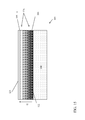
- FIG. 15 is a demonstrative illustration of a portion of a semiconductor device according to an embodiment of the invention.
- FIG. 16 is a demonstrative illustration of a flow diagram of a design process used in semiconductor design, manufacture, and/or test according to embodiments of the invention.
- FIG. 1 is a demonstrative illustration of a cross sectional view of a portion of a semiconductor device 100 according to embodiments of the invention.
- Semiconductor device 100 may include a substrate 140 , with a graded region 120 defined and/or formed thereon.
- Graded region 120 may include a plurality of materials and have a chemical concentration of material(s) which varies within the region to form a varied material concentration profile ‘G.’
- a metal layer 170 may be disposed on graded region 120 forming a metal gate 172 .
- Graded region 120 may include a first portion 122 in contact with substrate 140 , and a second portion 124 disposed above substrate 140 and first portion 122 .
- graded region 120 may include a high dielectric constant (high-K dielectric) region (e.g., a region with a high degree of permittivity relative other materials in semiconductor device 100 ).
- a concentration of the material(s) which comprise graded region 120 may vary gradually, linearly, incrementally, or exponentially between first portion 122 and second portion 124 .
- composition of graded region 120 at first portion 122 may be substantially silicon and composition of graded region 120 at second portion 124 may be substantially metal.
- graded region 120 may be deposited and/or formed directly on substrate 140 without an interface layer.
- graded region 120 may form a gate structure 126 .
- Silicates, metals and/or metal oxides may be deposited as part of graded region 120 .
- the term “depositing” may include any now known or later developed techniques appropriate for the material to be deposited including but are not limited to, for example: chemical vapor deposition (CVD), low-pressure CVD (LPCVD), plasma-enhanced CVD (PECVD), semi-atmosphere CVD (SACVD) and high density plasma CVD (HDPCVD), rapid thermal CVD (RTCVD), ultra-high vacuum CVD (UHVCVD), limited reaction processing CVD (LRPCVD), metalorganic CVD (MOCVD), sputtering deposition, ion beam deposition, electron beam deposition, laser-assisted deposition, thermal oxidation, thermal nitridation, spin-on methods, physical vapor deposition (PVD), atomic layer deposition (ALD), chemical oxidation, molecular beam
- CVD
- graded region 120 may be formed as a set of films (shown in FIG. 15 ) with a composition which is manipulated to generate a varied material concentration profile ‘G’ for graded region 120 .
- M is the metal composition (e.g., Aluminum, Magnesium, etc.) of graded region 120 at a given point ‘X’, Si the silicon composition of graded region 120 at given point X, and O y the oxide composition of graded region 120 at given point X.
- graded region 120 may include (e.g., contain) at least one of: aluminum (Al), magnesium (Mg), lanthanum (La), aluminum oxide (Al 2 O 3 ), lanthanum oxide (La 2 O 3 ), and zirconium oxide (Zr 2 O 3 ). It is understood that while specific material examples for graded region 120 are described herein, graded region 120 may include any combination of now known or later developed materials which provide the features described herein.
- metal composition M may include a plurality of metals (e.g., Aluminum, Hafnium Oxide (HfO 2 ), Magnesium, etc.).
- graded region 120 may include any commonly used dielectric and/or gate material including but not limited to polysilicon or high melting point refractory metals, such as W, Ti, Ta, Mo, Nb, Re, Ru and their binary or ternary metallic derivatives, e.g., WN, TiN, TaN, MoN, MoO2, TaSiN. Further, graded region 120 may comprise a gate structure 126 on semiconductor substrate 140 . Graded region 120 may comprise any commonly used gate dielectric material including but not limited to oxide, nitride, oxynitride, and high-k materials such as hafnium silicate, zirconium silicate, hafnium dioxide, and zirconium dioxide.
- graded region 120 may include silicon dioxide (SiO 2 ), silicon nitride (SiN), or any other material now known or later developed. Any number of dielectric regions may be located over the substrate, as many other layers included in semiconductor chips now known or later developed. In one embodiment, graded region 120 may include silicon dioxide (SiO 2 ) for its insulating, mechanical and optical qualities.
- Graded region 120 may also include, but is not limited to: silicon nitride (Si 3 N 4 ), fluorinated SiO 2 (FSG), hydrogenated silicon oxycarbide (SiCOH), porous SiCOH, boro-phosho-silicate glass (BPSG), silsesquioxanes, carbon (C) doped oxides (i.e., organosilicates) that include atoms of silicon (Si), carbon (C), oxygen (O), and/or hydrogen (H), thermosetting polyarylene ethers, SiLK (a polyarylene ether available from Dow Chemical Corporation), a spin-on silicon-carbon containing polymer material available from JSR Corporation, other low dielectric constant ( ⁇ 3.9) material, or layers thereof.
- SiLK a polyarylene ether available from Dow Chemical Corporation
- spin-on silicon-carbon containing polymer material available from JSR Corporation, other low dielectric constant ( ⁇ 3.9) material, or layers thereof.
- graded region 120 may be formed via a low temperature process which decreases the thermal budget of semiconductor device 100 and eliminates the need for an interface layer to thermally insulate substrate 140 , thereby making semiconductor device 100 replacement metal gate (RMG) compatible.
- Graded region 120 may include a first portion 122 adjacent substrate 140 which is substantially dielectric and a second portion 124 which is substantially metal.
- the controllable composition profile engineering provided by graded region 120 may enable linear and/or exponential gradation and variation of material concentration between first portion 122 at substrate 140 and second portion 124 .
- Use of graded region 120 may form a natural film stack between substrate 140 and the top of metal gate 172 , eliminating the interface formed by an interface layer.
- graded region 120 may be formed via an in-situ process (e.g., in the same process chamber used to perform other processes of forming semiconductor device 100 ) as a portion of the formation of semiconductor device 100 .
- Graded region 120 may be used to scale the leakage current and equivalent oxide thickness (EOT) of semiconductor device 100 via optimization, design and control of the material concentration profile G of semiconductor device 100 .
- EOT equivalent oxide thickness
- graded region 120 may be engineered to reduce the fixed charge and improve mobility via reduction of layer interfaces in semiconductor device 100 .
- the transitory material concentration profile G of graded region 120 reduces the number of interfaces between layers of semiconductor device 100 , providing a gradual transition between substrate 140 and metal layer 172 .
- nitrogen plasma and/or a rapid thermal (RT) ammonia (NH 3 ) anneal may be used to introduce Nitrogen into graded region 120 with desired profiles. This introduction may be included as a part of a nitridation process for graded region 120 .
- the material concentration profile G of graded region 120 may be controlled by manipulating at least one of a temperature, a pressure, and a duration of the NH 3 anneal.
- the material concentration profile G of graded region 120 may be controlled by manipulating at least one of a power, a pressure, and a temperature of the plasma process.
- a post anneal may be used following the plasma process for additional Nitrogen profile engineering.
- the material concentration profile G may be controlled by performing a series of nitridation and deposition processes with varying Nitrogen contents (e.g., separating nitrogen deposition into several stages of deposition divided by nitridation processes).
- the processes to provide substrate 140 as illustrated and described, are well known in the art and thus, no further description is necessary.
- graded region 120 includes a material concentration profile which is Silicon (Si) rich at a proximity to substrate 140 (e.g., first portion 122 ) and becomes Hafnium (Hf) rich proximate an extremity of graded region 120 opposite substrate 140 (e.g., second portion 124 ).
- FIG. 2 As can be seen in FIG. 2 , as the amount of Hf in graded region 120 increases the percentage of Si decreases.
- this graded HfO 2 dielectric e.g., graded region 120
- varying the material deposition composition relative a position ‘X’ in graded region 120 results in deposition of a controlled graded film with scaled equivalent oxide thickness (EOT).
- EOT scaled equivalent oxide thickness
- FIG. 3 a graphical representation of a material concentration profile of a graded region 120 is shown according to embodiments of the invention.
- graded material includes a non-linear material concentration profile which is Si rich proximate first portion 122 , and varies exponentially between first portion 122 and second portion 124 , becoming Hf rich proximate an extremity of graded region 120 opposite substrate 140 .
- semiconductor device 102 includes an interface layer 130 disposed between substrate 140 and graded region 120 .
- FIGS. 5-8 are demonstrative illustrations of a device undergoing a method according to embodiments of the invention. Although FIGS. 5-8 show the method of forming a portion of semiconductor device 100 in FIG. 1 , it is understood that a similar method may be employed to form semiconductor device 102 of FIG. 4 , or any other like semiconductor device.
- FIG. 5 a demonstrative illustration of a substrate 140 in semiconductor device 100 is shown in preparation for deposition of layers.
- Substrate 140 may include silicon or any other material commonly known and may be chemically cleaned.
- a trench 152 (shown in phantom) may be etched in substrate 140 .
- Trench 152 may be etched using any now known or later developed etching techniques.
- etching of substrate 140 may be performed using a reactive ion etch (RIE).
- RIE reactive ion etch
- RIE reactive ion etch
- RIE uses chemically reactive plasma to remove material deposited on wafers/substrates. Differences in width between these openings may allow for utilizing a phenomenon known as inverse RIE lag.
- Inverse RIE lag causes a faster etch rate in narrower openings (higher aspect ratios) than in openings having larger widths (lower aspect ratios).
- Inverse RIE lag may be induced under any conditions characterized by high polymerization and high wafer self-bias voltages.
- conditions characterized by high polymerization may include general chemistries such as CxHyFz (Carbon-Hydrogen-Flourine) with high oxide-to-nitride selectivity (where the blanket etch rate ratio is greater than approximately 20:1).
- conditions characterized by high polymerization may include O 2 (oxygen), a dilutant, and one or more of: C 4 F 6 , C 5 F 8 , or C 4 F 8 .
- the dilutant may be, for example, Argon (Ar).
- High wafer self-bias voltages may, for example, be voltages greater than approximately 500 volts. While specific conditions for facilitating inverse RIE lag are described herein, those conditions are merely illustrative. Inverse RIE lag may be induced under other conditions not specifically described herein.
- graded region 120 may be deposited as a set of films on substrate 140 , the films having a varied material composition relative to desired material concentration profile G.
- composition of graded region 120 at first portion 122 may be substantially silicon and composition of graded region 120 at second portion 124 may be substantially metal.
- semiconductor device 100 may be polished to develop the surfaces.
- graded region 120 may optionally be subjected to Nitrogen (N) plasma and/or RT NH 3 annealing 180 to introduce desired N profiles in graded region 120 and semiconductor device 100 .
- N Nitrogen
- This optional introduction of N further engineers material concentration profile G.
- a thermal anneal 182 may optionally be applied to semiconductor device 100 to stabilize the films that comprise graded region 120 .
- Stabilization of the films may produce semiconductor device 100 of FIG. 1 which includes a gate structure 126 formed by graded region 120 .
- Gate structure 126 may include a first portion 122 contacting substrate 140 and comprising substantially silicon (e.g., about 100% silicon), and a second portion 124 forming the top of gate structure 126 and comprising substantially metal (e.g., about 100% aluminum). Transition of material concentration/composition through graded region 120 between first portion 122 and second portion 124 may be linear (e.g., natural, gradual or incremental as shown in FIG. 2 ), exponential (e.g., irregular or varying as shown in FIG. 3 ), or any other form of gradation or transition known.
- FIGS. 9-14 are demonstrative illustrations of a semiconductor device 102 ( FIG. 4 ) undergoing processes according to a method in accordance with another embodiment of the invention. In this method an interface layer 130 is formed as a layer of semiconductor device 102 .
- FIGS. 9-14 are demonstrative illustrations of the method of forming a portion of semiconductor device 102 in FIG. 4 , it is understood that a similar method may be employed to form semiconductor device 100 of FIG. 1 , or any other like semiconductor device.
- a trench 152 may be etched in substrate 140 .
- trench 152 may be etched using any now known or later developed etching techniques.
- graded region 120 is deposited on substrate 140 .
- Graded region 120 may be deposited via PVD, ALD, CVD or any other known deposition techniques.
- graded region 120 may be deposited as a set of films on substrate 140 , the set of films having a varied material composition relative one another and being deposited in accordance with material concentration profile G.
- semiconductor device 100 may be polished to develop the surfaces.
- graded region 120 may optionally be subjected to N plasma and/or RT NH 3 annealing 180 to introduce desired N profiles in graded region 120 and semiconductor device 100 .
- a thermal anneal 182 may optionally be applied to semiconductor device 100 to stabilize the films that comprise graded region 120 .
- Stabilization of the films may produce semiconductor device 102 of FIG. 14 which includes a trench 152 disposed beneath gate structure 126 formed by graded region 120 .
- Gate structure 126 may include a first portion 128 contacting interface layer 130 and comprising substantially silicon (e.g., about 100% silicon), and a second portion 124 forming the top of the gate and comprising substantially metal (e.g., about 100% aluminum). Transition of material concentration/composition through graded region 120 between first portion 128 and second portion 124 may be linear (e.g., gradual or incremental as shown in FIG. 2 ), exponential (e.g., irregular or varying as shown in FIG. 3 ), or any other form of gradation or transition known.
- graded region 127 of semiconductor device 108 includes a plurality of films 186 to 186 +n disposed upon substrate 140 .
- Each film 186 to 186 +n in the plurality of films may comprise a varied material composition (e.g., specific proportions of silicon, metals, oxides, Nitrogen, etc.).
- Films 186 to 186 +n may be disposed upon substrate according to desired profile characteristics represented by material concentration profile G, defining the material composition profile of graded region 120 .
- film 186 may be deposited at first portion 122 with a composition of substantially silicon, then a film 186 +1 may be deposited on film 186 with a composition of about 95% to about 99% silicon, and about 1% to about 5% silicate (e.g., hafnium). As multiple layers are deposited on substrate 140 the proportions of silicon hafnium and any number of other materials and chemicals may be varied to control the material concentration profile of graded region 120 .
- film 186 +n may include hafnium nitride, thereby forming a high-K metal gate 172 .
- FIG. 16 is a demonstrative illustration of a flow diagram of an exemplary design flow 900 used for example, in semiconductor IC logic design, simulation, test, layout, and manufacture.
- Design flow 900 includes processes, machines and/or mechanisms for processing design structures or devices to generate logically or otherwise functionally equivalent representations of the design structures and/or devices described above and shown in FIG. 1 .
- the design structures processed and/or generated by design flow 900 may be encoded on machine-readable transmission or storage media to include data and/or instructions that when executed or otherwise processed on a data processing system generate a logically, structurally, mechanically, or otherwise functionally equivalent representation of hardware components, circuits, devices, or systems.
- Machines include, but are not limited to, any machine used in an IC design process, such as designing, manufacturing, or simulating a circuit, component, device, or system.
- machines may include: lithography machines, machines and/or equipment for generating masks (e.g. e-beam writers), computers or equipment for simulating design structures, any apparatus used in the manufacturing or test process, or any machines for programming functionally equivalent representations of the design structures into any medium (e.g. a machine for programming a programmable gate array).
- Design flow 900 may vary depending on the type of representation being designed. For example, a design flow 900 for building an application specific IC (ASIC) may differ from a design flow 900 for designing a standard component or from a design flow 900 for instantiating the design into a programmable array, for example a programmable gate array (PGA) or a field programmable gate array (FPGA).
- ASIC application specific IC
- PGA programmable gate array
- FPGA field programmable gate array
- FIG. 16 illustrates multiple such design structures including an input design structure 920 that is preferably processed by a design process 910 .
- Design structure 920 may be a logical simulation design structure generated and processed by design process 910 to produce a logically equivalent functional representation of a hardware device.
- Design structure 920 may also or alternatively comprise data and/or program instructions that when processed by design process 910 , generate a functional representation of the physical structure of a hardware device. Whether representing functional and/or structural design features, design structure 920 may be generated using electronic computer-aided design (ECAD) such as implemented by a core developer/designer.
- ECAD electronic computer-aided design
- design structure 920 When encoded on a machine-readable data transmission, gate array, or storage medium, design structure 920 may be accessed and processed by one or more hardware and/or software modules within design process 910 to simulate or otherwise functionally represent an electronic component, circuit, electronic or logic module, apparatus, device, or system such as those shown in FIG. 1 .
- design structure 920 may comprise files or other data structures including human and/or machine-readable source code, compiled structures, and computer-executable code structures that when processed by a design or simulation data processing system, functionally simulate or otherwise represent circuits or other levels of hardware logic design.
- data structures may include hardware-description language (HDL) design entities or other data structures conforming to and/or compatible with lower-level HDL design languages such as Verilog and VHDL, and/or higher level design languages such as C or C++.
- HDL hardware-description language
- Design process 910 preferably employs and incorporates hardware and/or software modules for synthesizing, translating, or otherwise processing a design/simulation functional equivalent of the components, circuits, devices, or logic structures shown in FIG. 1 to generate a netlist 980 which may contain design structures such as design structure 920 .
- Netlist 980 may comprise, for example, compiled or otherwise processed data structures representing a list of wires, discrete components, logic gates, control circuits, I/O devices, models, etc. that describes the connections to other elements and circuits in an integrated circuit design.
- Netlist 980 may be synthesized using an iterative process in which netlist 980 is resynthesized one or more times depending on design specifications and parameters for the device.
- netlist 980 may be recorded on a machine-readable data storage medium or programmed into a programmable gate array.
- the medium may be a non-volatile storage medium such as a magnetic or optical disk drive, a programmable gate array, a compact flash, or other flash memory. Additionally, or in the alternative, the medium may be a system or cache memory, buffer space, or electrically or optically conductive devices and materials on which data packets may be transmitted and intermediately stored via the Internet, or other networking suitable means.
- Design process 910 may include hardware and software modules for processing a variety of input data structure types including netlist 980 .
- data structure types may reside, for example, within library elements 930 and include a set of commonly used elements, circuits, and devices, including models, layouts, and symbolic representations, for a given manufacturing technology (e.g., different technology nodes, 32 nm, 45 nm, 90 nm, etc.).
- the data structure types may further include design specifications 940 , characterization data 950 , verification data 960 , design rules 970 , and test data files 985 which may include input test patterns, output test results, and other testing information.
- Design process 910 may further include, for example, standard mechanical design processes such as stress analysis, thermal analysis, mechanical event simulation, process simulation for operations such as casting, molding, and die press forming, etc.
- standard mechanical design processes such as stress analysis, thermal analysis, mechanical event simulation, process simulation for operations such as casting, molding, and die press forming, etc.
- One of ordinary skill in the art of mechanical design can appreciate the extent of possible mechanical design tools and applications used in design process 910 without deviating from the scope and spirit of the invention.
- Design process 910 may also include modules for performing standard circuit design processes such as timing analysis, verification, design rule checking, place and route operations, etc.
- Design process 910 employs and incorporates logic and physical design tools such as HDL compilers and simulation model build tools to process design structure 920 together with some or all of the depicted supporting data structures along with any additional mechanical design or data (if applicable), to generate a second design structure 990 .
- Design structure 990 resides on a storage medium or programmable gate array in a data format used for the exchange of data of mechanical devices and structures (e.g. information stored in a IGES, DXF, Parasolid XT, JT, DRG, or any other suitable format for storing or rendering such mechanical design structures).
- design structure 990 preferably comprises one or more files, data structures, or other computer-encoded data or instructions that reside on transmission or data storage media and that when processed by an ECAD system generate a logically or otherwise functionally equivalent form of one or more of the embodiments of the invention shown in FIG. 1 .
- design structure 990 may comprise a compiled, executable HDL simulation model that functionally simulates the devices shown in FIG. 1 .
- Design structure 990 may also employ a data format used for the exchange of layout data of integrated circuits and/or symbolic data format (e.g. information stored in a GDSII (GDS 2 ), GL 1 , OASIS, map files, or any other suitable format for storing such design data structures).
- Design structure 990 may comprise information such as, for example, symbolic data, map files, test data files, design content files, manufacturing data, layout parameters, wires, levels of metal, vias, shapes, data for routing through the manufacturing line, and any other data required by a manufacturer or other designer/developer to produce a device or structure as described above and shown in FIG. 1 .
- Design structure 990 may then proceed to a stage 995 where, for example, design structure 990 : proceeds to tape-out, is released to manufacturing, is released to a mask house, is sent to another design house, is sent back to the customer, etc.
- the circuit as described above is part of the design for an integrated circuit chip.
- the chip design is created in a graphical computer programming language, and stored in a computer storage medium (such as a disk, tape, physical hard drive, or virtual hard drive such as in a storage access network). If the designer does not fabricate chips or the photolithographic masks used to fabricate chips, the designer transmits the resulting design by physical means (e.g., by providing a copy of the storage medium storing the design) or electronically (e.g., through the Internet) to such entities, directly or indirectly.
- the stored design is then converted into the appropriate format (e.g., GDSII) for the fabrication of photolithographic masks, which typically include multiple copies of the chip design in question that are to be formed on a wafer.
- the photolithographic masks are utilized to define areas of the wafer (and/or the layers thereon) to be etched or otherwise processed.
- the method as described above is used in the fabrication of integrated circuit chips.
- the resulting integrated circuit chips can be distributed by the fabricator in raw wafer form (that is, as a single wafer that has multiple unpackaged chips), as a bare die, or in a packaged form.
- the chip is mounted in a single chip package (such as a plastic carrier, with leads that are affixed to a motherboard or other higher level carrier) or in a multichip package (such as a ceramic carrier that has either or both surface interconnections or buried interconnections).
- the chip is then integrated with other chips, discrete circuit elements, and/or other signal processing devices as part of either (a) an intermediate product, such as a motherboard, or (b) an end product.
- the end product can be any product that includes integrated circuit chips, ranging from toys and other low-end applications to advanced computer products having a display, a keyboard or other input device, and a central processor.
Abstract
Description
Material Composition=MXSi1-XOy Eq. 1
Where M is the metal composition (e.g., Aluminum, Magnesium, etc.) of graded
Material Composition=HfXSi1-XOy Eq. 2
Claims (8)
Priority Applications (1)
| Application Number | Priority Date | Filing Date | Title |
|---|---|---|---|
| US14/081,417 US9257519B2 (en) | 2012-04-23 | 2013-11-15 | Semiconductor device including graded gate stack, related method and design structure |
Applications Claiming Priority (2)
| Application Number | Priority Date | Filing Date | Title |
|---|---|---|---|
| US13/453,131 US20130277765A1 (en) | 2012-04-23 | 2012-04-23 | Semiconductor device including graded gate stack, related method and design structure |
| US14/081,417 US9257519B2 (en) | 2012-04-23 | 2013-11-15 | Semiconductor device including graded gate stack, related method and design structure |
Related Parent Applications (1)
| Application Number | Title | Priority Date | Filing Date |
|---|---|---|---|
| US13/453,131 Division US20130277765A1 (en) | 2012-04-23 | 2012-04-23 | Semiconductor device including graded gate stack, related method and design structure |
Publications (2)
| Publication Number | Publication Date |
|---|---|
| US20140070334A1 US20140070334A1 (en) | 2014-03-13 |
| US9257519B2 true US9257519B2 (en) | 2016-02-09 |
Family
ID=49379316
Family Applications (2)
| Application Number | Title | Priority Date | Filing Date |
|---|---|---|---|
| US13/453,131 Abandoned US20130277765A1 (en) | 2012-04-23 | 2012-04-23 | Semiconductor device including graded gate stack, related method and design structure |
| US14/081,417 Expired - Fee Related US9257519B2 (en) | 2012-04-23 | 2013-11-15 | Semiconductor device including graded gate stack, related method and design structure |
Family Applications Before (1)
| Application Number | Title | Priority Date | Filing Date |
|---|---|---|---|
| US13/453,131 Abandoned US20130277765A1 (en) | 2012-04-23 | 2012-04-23 | Semiconductor device including graded gate stack, related method and design structure |
Country Status (1)
| Country | Link |
|---|---|
| US (2) | US20130277765A1 (en) |
Cited By (1)
| Publication number | Priority date | Publication date | Assignee | Title |
|---|---|---|---|---|
| US11605724B2 (en) | 2021-04-15 | 2023-03-14 | Kabushiki Kaisha Toshiba | Semiconductor device |
Families Citing this family (4)
| Publication number | Priority date | Publication date | Assignee | Title |
|---|---|---|---|---|
| TWI549163B (en) * | 2011-09-20 | 2016-09-11 | 應用材料股份有限公司 | Surface stabilization process to reduce dopant diffusion |
| US9275853B2 (en) | 2013-07-29 | 2016-03-01 | Applied Materials, Inc. | Method of adjusting a transistor gate flat band voltage with addition of AL203 on nitrided silicon channel |
| US10062693B2 (en) | 2016-02-24 | 2018-08-28 | International Business Machines Corporation | Patterned gate dielectrics for III-V-based CMOS circuits |
| US10593600B2 (en) | 2016-02-24 | 2020-03-17 | International Business Machines Corporation | Distinct gate stacks for III-V-based CMOS circuits comprising a channel cap |
Citations (24)
| Publication number | Priority date | Publication date | Assignee | Title |
|---|---|---|---|---|
| US5637514A (en) * | 1995-10-18 | 1997-06-10 | Micron Technology, Inc. | Method of forming a field effect transistor |
| US6020243A (en) * | 1997-07-24 | 2000-02-01 | Texas Instruments Incorporated | Zirconium and/or hafnium silicon-oxynitride gate dielectric |
| US6100559A (en) * | 1998-08-14 | 2000-08-08 | Advanced Micro Devices, Inc. | Multipurpose graded silicon oxynitride cap layer |
| US6207995B1 (en) * | 1999-02-23 | 2001-03-27 | Advanced Micro Devices, Inc. | High K integration of gate dielectric with integrated spacer formation for high speed CMOS |
| US6297106B1 (en) * | 1999-05-07 | 2001-10-02 | Chartered Semiconductor Manufacturing Ltd. | Transistors with low overlap capacitance |
| US20010041250A1 (en) * | 2000-03-07 | 2001-11-15 | Werkhoven Christian J. | Graded thin films |
| US20020022325A1 (en) * | 1998-01-05 | 2002-02-21 | Advanced Micro Devices, Inc. | Method of making ultra thin oxide formation using selective etchback technique integrated with thin nitride layer for high performance mosfet |
| US20020048910A1 (en) * | 2000-05-26 | 2002-04-25 | Taylor, Jr. William J. | Method and apparatus for forming a semiconductor device utilizing a low temperature process |
| US20020061637A1 (en) * | 2000-04-14 | 2002-05-23 | Fuchao Wang | Graded/stepped silicide process to improve mos transistor |
| US6451658B2 (en) * | 1998-08-21 | 2002-09-17 | Micron Technology, Inc. | Graded layer for use in semiconductor circuits and method for making same |
| US6770923B2 (en) | 2001-03-20 | 2004-08-03 | Freescale Semiconductor, Inc. | High K dielectric film |
| US6911707B2 (en) | 1998-12-09 | 2005-06-28 | Advanced Micro Devices, Inc. | Ultrathin high-K gate dielectric with favorable interface properties for improved semiconductor device performance |
| US20050260357A1 (en) * | 2004-05-21 | 2005-11-24 | Applied Materials, Inc. | Stabilization of high-k dielectric materials |
| US7084038B2 (en) | 2004-09-07 | 2006-08-01 | Intel Corporation | Method for making a semiconductor device having a high-k gate dielectric |
| US7105886B2 (en) | 2003-11-12 | 2006-09-12 | Freescale Semiconductor, Inc. | High K dielectric film |
| US20070018214A1 (en) * | 2005-07-25 | 2007-01-25 | Micron Technology, Inc. | Magnesium titanium oxide films |
| US20070048953A1 (en) * | 2005-08-30 | 2007-03-01 | Micron Technology, Inc. | Graded dielectric layers |
| US7198999B2 (en) | 2004-04-29 | 2007-04-03 | Micron Technology, Inc. | Flash memory device having a graded composition, high dielectric constant gate insulator |
| US20070102776A1 (en) * | 2005-11-09 | 2007-05-10 | Advanced Micro Devices, Inc. | Replacement metal gate transistors with reduced gate oxide leakage |
| US20090195152A1 (en) * | 2008-02-06 | 2009-08-06 | Mitsuru Sawano | Luminescent device and method of producing the same |
| US20100078738A1 (en) | 2008-09-30 | 2010-04-01 | Texas Instruments Incorporated | Method to Maximize Nitrogen Concentration at the Top Surface of Gate Dielectrics |
| US7776701B2 (en) | 2005-12-19 | 2010-08-17 | International Business Machines Corporation | Metal oxynitride as a pFET material |
| US20100320476A1 (en) * | 2009-06-19 | 2010-12-23 | Semisouth Laboratories, Inc. | Vertical junction field effect transistors and diodes having graded doped regions and methods of making |
| US20110256718A1 (en) | 2000-03-07 | 2011-10-20 | Asm International N.V. | Thin films |
-
2012
- 2012-04-23 US US13/453,131 patent/US20130277765A1/en not_active Abandoned
-
2013
- 2013-11-15 US US14/081,417 patent/US9257519B2/en not_active Expired - Fee Related
Patent Citations (25)
| Publication number | Priority date | Publication date | Assignee | Title |
|---|---|---|---|---|
| US5637514A (en) * | 1995-10-18 | 1997-06-10 | Micron Technology, Inc. | Method of forming a field effect transistor |
| US6020243A (en) * | 1997-07-24 | 2000-02-01 | Texas Instruments Incorporated | Zirconium and/or hafnium silicon-oxynitride gate dielectric |
| US20020022325A1 (en) * | 1998-01-05 | 2002-02-21 | Advanced Micro Devices, Inc. | Method of making ultra thin oxide formation using selective etchback technique integrated with thin nitride layer for high performance mosfet |
| US6100559A (en) * | 1998-08-14 | 2000-08-08 | Advanced Micro Devices, Inc. | Multipurpose graded silicon oxynitride cap layer |
| US6451658B2 (en) * | 1998-08-21 | 2002-09-17 | Micron Technology, Inc. | Graded layer for use in semiconductor circuits and method for making same |
| US6911707B2 (en) | 1998-12-09 | 2005-06-28 | Advanced Micro Devices, Inc. | Ultrathin high-K gate dielectric with favorable interface properties for improved semiconductor device performance |
| US6207995B1 (en) * | 1999-02-23 | 2001-03-27 | Advanced Micro Devices, Inc. | High K integration of gate dielectric with integrated spacer formation for high speed CMOS |
| US6297106B1 (en) * | 1999-05-07 | 2001-10-02 | Chartered Semiconductor Manufacturing Ltd. | Transistors with low overlap capacitance |
| US20010041250A1 (en) * | 2000-03-07 | 2001-11-15 | Werkhoven Christian J. | Graded thin films |
| US20110256718A1 (en) | 2000-03-07 | 2011-10-20 | Asm International N.V. | Thin films |
| US20020061637A1 (en) * | 2000-04-14 | 2002-05-23 | Fuchao Wang | Graded/stepped silicide process to improve mos transistor |
| US20020048910A1 (en) * | 2000-05-26 | 2002-04-25 | Taylor, Jr. William J. | Method and apparatus for forming a semiconductor device utilizing a low temperature process |
| US6770923B2 (en) | 2001-03-20 | 2004-08-03 | Freescale Semiconductor, Inc. | High K dielectric film |
| US7105886B2 (en) | 2003-11-12 | 2006-09-12 | Freescale Semiconductor, Inc. | High K dielectric film |
| US7198999B2 (en) | 2004-04-29 | 2007-04-03 | Micron Technology, Inc. | Flash memory device having a graded composition, high dielectric constant gate insulator |
| US20050260357A1 (en) * | 2004-05-21 | 2005-11-24 | Applied Materials, Inc. | Stabilization of high-k dielectric materials |
| US7709909B2 (en) | 2004-09-07 | 2010-05-04 | Intel Corporation | Method for making a semiconductor device having a high-k gate dielectric |
| US7084038B2 (en) | 2004-09-07 | 2006-08-01 | Intel Corporation | Method for making a semiconductor device having a high-k gate dielectric |
| US20070018214A1 (en) * | 2005-07-25 | 2007-01-25 | Micron Technology, Inc. | Magnesium titanium oxide films |
| US20070048953A1 (en) * | 2005-08-30 | 2007-03-01 | Micron Technology, Inc. | Graded dielectric layers |
| US20070102776A1 (en) * | 2005-11-09 | 2007-05-10 | Advanced Micro Devices, Inc. | Replacement metal gate transistors with reduced gate oxide leakage |
| US7776701B2 (en) | 2005-12-19 | 2010-08-17 | International Business Machines Corporation | Metal oxynitride as a pFET material |
| US20090195152A1 (en) * | 2008-02-06 | 2009-08-06 | Mitsuru Sawano | Luminescent device and method of producing the same |
| US20100078738A1 (en) | 2008-09-30 | 2010-04-01 | Texas Instruments Incorporated | Method to Maximize Nitrogen Concentration at the Top Surface of Gate Dielectrics |
| US20100320476A1 (en) * | 2009-06-19 | 2010-12-23 | Semisouth Laboratories, Inc. | Vertical junction field effect transistors and diodes having graded doped regions and methods of making |
Non-Patent Citations (5)
| Title |
|---|
| Chowdhury et al., High-k Dielectrics for Submicron MOSFET, Jul. 2010, pp. 1-12, vol. 2, IJETSE. |
| Kang et al., Scaling down of ultrathin HfO2 gate dielectrics by using a nitrided Si surface, Apr. 16, 2004, pp. 916-919 American Vacuum Society. |
| Kirsch et al. Nucleation and growth study of atomic layer deposited HfO2 gate dielectrics resulting in improved scaling and electron mobility, 2006, 9 pages, American Institute of Physics. |
| U.S. Appl. No. 13/452,131, Office Action dated Mar. 20, 2014. |
| U.S. Appl. No. 13/453,131, Office Action dated Aug. 14, 2013. |
Cited By (1)
| Publication number | Priority date | Publication date | Assignee | Title |
|---|---|---|---|---|
| US11605724B2 (en) | 2021-04-15 | 2023-03-14 | Kabushiki Kaisha Toshiba | Semiconductor device |
Also Published As
| Publication number | Publication date |
|---|---|
| US20140070334A1 (en) | 2014-03-13 |
| US20130277765A1 (en) | 2013-10-24 |
Similar Documents
| Publication | Publication Date | Title |
|---|---|---|
| US8390079B2 (en) | Sealed air gap for semiconductor chip | |
| TWI675436B (en) | Ic structure with interface liner and methods of forming same | |
| US8084346B1 (en) | Replacement metal gate method | |
| US9257519B2 (en) | Semiconductor device including graded gate stack, related method and design structure | |
| US8435891B2 (en) | Converting metal mask to metal-oxide etch stop layer and related semiconductor structure | |
| CN102110650A (en) | Semiconductor device and manufacturing method thereof | |
| CN103107091A (en) | Semiconductor structure and manufacture method thereof | |
| WO2009088588A2 (en) | Methods for fabricating pmos metal gate structures | |
| US8003463B2 (en) | Structure, design structure and method of manufacturing dual metal gate Vt roll-up structure | |
| KR20100073965A (en) | Band edge engineered vt offset device | |
| US8912597B2 (en) | Semiconductor device including asymmetric lightly doped drain (LDD) region, related method and design structure | |
| US9171844B2 (en) | Gate structures and methods of manufacture | |
| US8912630B2 (en) | Integrated circuit including thermal gate, related method and design structure | |
| US8809998B2 (en) | Semiconductor device including in wafer inductors, related method and design structure | |
| US9099461B2 (en) | Method of manufacturing scaled equivalent oxide thickness gate stacks in semiconductor devices and related design structure | |
| US9041105B2 (en) | Integrated circuit including transistor structure on depleted silicon-on-insulator, related method and design structure | |
| CN103137456B (en) | The manufacture method of PMOS transistor metal gates | |
| US7964922B2 (en) | Structure, design structure and method of manufacturing dual metal gate VT roll-up structure | |
| US9230857B2 (en) | Method to improve semiconductor surfaces and polishing | |
| US8564074B2 (en) | Self-limiting oxygen seal for high-K dielectric and design structure | |
| US9412640B2 (en) | Semiconductor device including substrate contact and related method | |
| US8735244B2 (en) | Semiconductor device devoid of an interfacial layer and methods of manufacture | |
| US20210057559A1 (en) | Back end of line nanowire power switch transistors | |
| US8835292B2 (en) | Method of manufacturing semiconductor devices including replacement metal gate process incorporating a conductive dummy gate layer | |
| US8766378B2 (en) | Programmable FETs using Vt-shift effect and methods of manufacture |
Legal Events
| Date | Code | Title | Description |
|---|---|---|---|
| AS | Assignment |
Owner name: INTERNATIONAL BUSINESS MACHINES CORPORATION, NEW Y Free format text: ASSIGNMENT OF ASSIGNORS INTEREST;ASSIGNORS:CHUDZIK, MICHAEL P.;DAI, MIN;SHEPARD, JOSEPH F., JR.;AND OTHERS;SIGNING DATES FROM 20131122 TO 20140305;REEL/FRAME:032517/0141 Owner name: GLOBALFOUNDRIES INC., CAYMAN ISLANDS Free format text: ASSIGNMENT OF ASSIGNORS INTEREST;ASSIGNOR:LIU, JINPING;REEL/FRAME:032517/0531 Effective date: 20131217 |
|
| AS | Assignment |
Owner name: GLOBALFOUNDRIES U.S. 2 LLC, NEW YORK Free format text: ASSIGNMENT OF ASSIGNORS INTEREST;ASSIGNOR:INTERNATIONAL BUSINESS MACHINES CORPORATION;REEL/FRAME:036550/0001 Effective date: 20150629 |
|
| AS | Assignment |
Owner name: GLOBALFOUNDRIES INC., CAYMAN ISLANDS Free format text: ASSIGNMENT OF ASSIGNORS INTEREST;ASSIGNORS:GLOBALFOUNDRIES U.S. 2 LLC;GLOBALFOUNDRIES U.S. INC.;REEL/FRAME:036779/0001 Effective date: 20150910 |
|
| STCF | Information on status: patent grant |
Free format text: PATENTED CASE |
|
| AS | Assignment |
Owner name: WILMINGTON TRUST, NATIONAL ASSOCIATION, DELAWARE Free format text: SECURITY AGREEMENT;ASSIGNOR:GLOBALFOUNDRIES INC.;REEL/FRAME:049490/0001 Effective date: 20181127 |
|
| FEPP | Fee payment procedure |
Free format text: MAINTENANCE FEE REMINDER MAILED (ORIGINAL EVENT CODE: REM.); ENTITY STATUS OF PATENT OWNER: LARGE ENTITY |
|
| LAPS | Lapse for failure to pay maintenance fees |
Free format text: PATENT EXPIRED FOR FAILURE TO PAY MAINTENANCE FEES (ORIGINAL EVENT CODE: EXP.); ENTITY STATUS OF PATENT OWNER: LARGE ENTITY |
|
| STCH | Information on status: patent discontinuation |
Free format text: PATENT EXPIRED DUE TO NONPAYMENT OF MAINTENANCE FEES UNDER 37 CFR 1.362 |
|
| FP | Lapsed due to failure to pay maintenance fee |
Effective date: 20200209 |
|
| AS | Assignment |
Owner name: GLOBALFOUNDRIES INC., CAYMAN ISLANDS Free format text: RELEASE BY SECURED PARTY;ASSIGNOR:WILMINGTON TRUST, NATIONAL ASSOCIATION;REEL/FRAME:054636/0001 Effective date: 20201117 |
|
| AS | Assignment |
Owner name: GLOBALFOUNDRIES U.S. INC., NEW YORK Free format text: RELEASE BY SECURED PARTY;ASSIGNOR:WILMINGTON TRUST, NATIONAL ASSOCIATION;REEL/FRAME:056987/0001 Effective date: 20201117 |