US9281345B2 - Resistance change type memory device with three-dimensional structure - Google Patents
Resistance change type memory device with three-dimensional structure Download PDFInfo
- Publication number
- US9281345B2 US9281345B2 US14/107,442 US201314107442A US9281345B2 US 9281345 B2 US9281345 B2 US 9281345B2 US 201314107442 A US201314107442 A US 201314107442A US 9281345 B2 US9281345 B2 US 9281345B2
- Authority
- US
- United States
- Prior art keywords
- wiring
- memory
- bit line
- wirings
- local bit
- Prior art date
- Legal status (The legal status is an assumption and is not a legal conclusion. Google has not performed a legal analysis and makes no representation as to the accuracy of the status listed.)
- Active, expires
Links
Images


Classifications
-
- H01L27/2436—
-
- H—ELECTRICITY
- H10—SEMICONDUCTOR DEVICES; ELECTRIC SOLID-STATE DEVICES NOT OTHERWISE PROVIDED FOR
- H10B—ELECTRONIC MEMORY DEVICES
- H10B63/00—Resistance change memory devices, e.g. resistive RAM [ReRAM] devices
- H10B63/30—Resistance change memory devices, e.g. resistive RAM [ReRAM] devices comprising selection components having three or more electrodes, e.g. transistors
-
- H01L27/249—
-
- H01L45/10—
-
- H01L45/1226—
-
- H01L45/14—
-
- H01L45/145—
-
- H01L45/16—
-
- H01L45/1616—
-
- H01L45/1675—
-
- H—ELECTRICITY
- H10—SEMICONDUCTOR DEVICES; ELECTRIC SOLID-STATE DEVICES NOT OTHERWISE PROVIDED FOR
- H10B—ELECTRONIC MEMORY DEVICES
- H10B63/00—Resistance change memory devices, e.g. resistive RAM [ReRAM] devices
- H10B63/30—Resistance change memory devices, e.g. resistive RAM [ReRAM] devices comprising selection components having three or more electrodes, e.g. transistors
- H10B63/34—Resistance change memory devices, e.g. resistive RAM [ReRAM] devices comprising selection components having three or more electrodes, e.g. transistors of the vertical channel field-effect transistor type
-
- H—ELECTRICITY
- H10—SEMICONDUCTOR DEVICES; ELECTRIC SOLID-STATE DEVICES NOT OTHERWISE PROVIDED FOR
- H10B—ELECTRONIC MEMORY DEVICES
- H10B63/00—Resistance change memory devices, e.g. resistive RAM [ReRAM] devices
- H10B63/80—Arrangements comprising multiple bistable or multi-stable switching components of the same type on a plane parallel to the substrate, e.g. cross-point arrays
- H10B63/84—Arrangements comprising multiple bistable or multi-stable switching components of the same type on a plane parallel to the substrate, e.g. cross-point arrays arranged in a direction perpendicular to the substrate, e.g. 3D cell arrays
- H10B63/845—Arrangements comprising multiple bistable or multi-stable switching components of the same type on a plane parallel to the substrate, e.g. cross-point arrays arranged in a direction perpendicular to the substrate, e.g. 3D cell arrays the switching components being connected to a common vertical conductor
-
- H—ELECTRICITY
- H10—SEMICONDUCTOR DEVICES; ELECTRIC SOLID-STATE DEVICES NOT OTHERWISE PROVIDED FOR
- H10N—ELECTRIC SOLID-STATE DEVICES NOT OTHERWISE PROVIDED FOR
- H10N70/00—Solid-state devices without a potential-jump barrier or surface barrier, and specially adapted for rectifying, amplifying, oscillating or switching
- H10N70/011—Manufacture or treatment of multistable switching devices
- H10N70/021—Formation of the switching material, e.g. layer deposition
- H10N70/023—Formation of the switching material, e.g. layer deposition by chemical vapor deposition, e.g. MOCVD, ALD
-
- H—ELECTRICITY
- H10—SEMICONDUCTOR DEVICES; ELECTRIC SOLID-STATE DEVICES NOT OTHERWISE PROVIDED FOR
- H10N—ELECTRIC SOLID-STATE DEVICES NOT OTHERWISE PROVIDED FOR
- H10N70/00—Solid-state devices without a potential-jump barrier or surface barrier, and specially adapted for rectifying, amplifying, oscillating or switching
- H10N70/011—Manufacture or treatment of multistable switching devices
- H10N70/061—Patterning of the switching material
- H10N70/063—Patterning of the switching material by etching of pre-deposited switching material layers, e.g. lithography
-
- H—ELECTRICITY
- H10—SEMICONDUCTOR DEVICES; ELECTRIC SOLID-STATE DEVICES NOT OTHERWISE PROVIDED FOR
- H10N—ELECTRIC SOLID-STATE DEVICES NOT OTHERWISE PROVIDED FOR
- H10N70/00—Solid-state devices without a potential-jump barrier or surface barrier, and specially adapted for rectifying, amplifying, oscillating or switching
- H10N70/20—Multistable switching devices, e.g. memristors
- H10N70/24—Multistable switching devices, e.g. memristors based on migration or redistribution of ionic species, e.g. anions, vacancies
- H10N70/245—Multistable switching devices, e.g. memristors based on migration or redistribution of ionic species, e.g. anions, vacancies the species being metal cations, e.g. programmable metallization cells
-
- H—ELECTRICITY
- H10—SEMICONDUCTOR DEVICES; ELECTRIC SOLID-STATE DEVICES NOT OTHERWISE PROVIDED FOR
- H10N—ELECTRIC SOLID-STATE DEVICES NOT OTHERWISE PROVIDED FOR
- H10N70/00—Solid-state devices without a potential-jump barrier or surface barrier, and specially adapted for rectifying, amplifying, oscillating or switching
- H10N70/20—Multistable switching devices, e.g. memristors
- H10N70/25—Multistable switching devices, e.g. memristors based on bulk electronic defects, e.g. trapping of electrons
-
- H—ELECTRICITY
- H10—SEMICONDUCTOR DEVICES; ELECTRIC SOLID-STATE DEVICES NOT OTHERWISE PROVIDED FOR
- H10N—ELECTRIC SOLID-STATE DEVICES NOT OTHERWISE PROVIDED FOR
- H10N70/00—Solid-state devices without a potential-jump barrier or surface barrier, and specially adapted for rectifying, amplifying, oscillating or switching
- H10N70/801—Constructional details of multistable switching devices
- H10N70/821—Device geometry
- H10N70/823—Device geometry adapted for essentially horizontal current flow, e.g. bridge type devices
-
- H—ELECTRICITY
- H10—SEMICONDUCTOR DEVICES; ELECTRIC SOLID-STATE DEVICES NOT OTHERWISE PROVIDED FOR
- H10N—ELECTRIC SOLID-STATE DEVICES NOT OTHERWISE PROVIDED FOR
- H10N70/00—Solid-state devices without a potential-jump barrier or surface barrier, and specially adapted for rectifying, amplifying, oscillating or switching
- H10N70/801—Constructional details of multistable switching devices
- H10N70/881—Switching materials
- H10N70/883—Oxides or nitrides
- H10N70/8833—Binary metal oxides, e.g. TaOx
Definitions
- Embodiments are generally related to a non-volatile memory device.
- a memory cell array having a three-dimensional structure has been studied for realizing next-generation non-volatile memory devices.
- a memory cell array may include bit lines extending in the direction perpendicular to an underlayer, and memory cells are disposed along each bit line.
- the memory cells may include a storage layer provided on the sidewall of the bit line.
- FIG. 1 is a schematic perspective view showing an example of a memory cell array of a non-volatile memory device according to a first embodiment
- FIG. 2 is a transparent plan view schematically showing one example of the memory cell array according to the first embodiment
- FIG. 3 is a block diagram showing the non-volatile memory device according to the first embodiment
- FIG. 4 is a cross-sectional view schematically showing one example of the memory cell array according to the first embodiment
- FIGS. 5A and 5B are schematic diagrams showing a memory cell array according to a comparative example
- FIGS. 6A and 6B are schematic diagrams showing one example of the memory cell array according to the first embodiment
- FIGS. 7 to 11C are schematic views showing one example of the manufacturing process of the memory cell array according to the first embodiment
- FIG. 12 is a schematic cross-sectional view showing one example of a memory cell array according to a variation of the first embodiment
- FIGS. 13A to 13C are schematic diagrams showing a memory cell array according to another variation of the first embodiment
- FIG. 14 is a cross-sectional view schematically showing one example of a memory cell array according to a second embodiment.
- FIG. 15 is a schematic cross-sectional view showing one example of a memory cell array of a non-volatile memory device according to a third embodiment.
- a non-volatile memory device includes a first wiring extending in a first direction, a second wiring extending in a second direction orthogonal to the first direction, and electrically connected to the first wiring.
- the device includes third wirings, a first memory and a second memory.
- a pair of third wirings extend in a third direction crossing the first direction and orthogonal to the second direction, aligned in the second direction on both sides of the second wiring, and face each other across the second wiring.
- the first memory is provided between one of the third wiring pair and the second wiring.
- the second memory is provided between another one of the third wiring pair and the second wiring.
- the second wiring has a block portion between a first portion in contact with the first memory and a second portion in contact with the second memory.
- the arrangement of components are described with reference to the three axis directions orthogonal to one another as shown in the drawings, namely, the X-direction, the Y-direction, and the Z-direction.
- the Z-direction may be described as upward, and the direction opposite thereto may be described downward.
- a non-volatile memory device 100 includes a memory cell array 1 of a three-dimensional structure.
- the memory cell array 1 includes memory cells (MCs) of resistance change type, for example.
- the non-volatile memory device 100 according to the first embodiment will now be described with reference to FIG. 1 to FIG. 4 .
- FIG. 1 is a schematic perspective view showing an example of the memory cell array 1 .
- the memory cell array 1 includes a first wiring extending in a first direction, and a second wiring extending in a second direction orthogonal to the first direction.
- the second wiring is electrically connected to the first wiring.
- the memory cell array 1 also includes third wirings extending in a third direction intersecting the first direction and orthogonal to the second direction.
- the first direction is the X-direction
- the second direction is the Z-direction
- the third direction is the Y-direction.
- the extending directions of the wirings are orthogonal to one another, but are not limited to orthogonal in a strict sense. For example, it is sufficient to be an approximately orthogonal state in which some shifts from orthogonal due to manufacturing techniques etc. are allowable.
- the third direction is not limited to the Y-direction orthogonal to the X-direction, and it is sufficient to be a direction intersecting the X-direction in the X-Y plane.
- the first wiring is a global bit line 10 and extends in the X-direction, for example.
- the memory cell array 1 includes a plurality of global bit lines 10 .
- the global bit lines 10 are provided parallel to one another and are arranged to be aligned in the Y-direction.
- the second wiring is a local bit line 20 and extends in the Z-direction, for example.
- the local bit line 20 is electrically connected to the global bit line 10 via a select element 50 , for example, a thin film transistor (TFT).
- a plurality of local bit lines 20 are electrically connected to one global bit line 10 .
- the third wiring is a word line 30 and extends in the Y-direction, for example.
- the memory cell array 1 includes a plurality of word lines 30 .
- the word line 30 is provided on both sides of the local bit line 20 .
- the word lines 30 are provided parallel to one another on each side and are arranged to be aligned in the Z-direction.
- a memory layer 40 is provided between the local bit line 20 and the word line 30 .
- the memory layer 40 contains a resistance change material that reversibly transitions between a first state and a second state having electrical resistance lower than the first state, for example.
- the resistance change material contains, for example, an oxide of at least one element selected from the group consisting of hafnium (Hf), zirconium (Zr), nickel (Ni), tantalum (Ta), tungsten (W), cobalt (Co), aluminum (Al), iron (Fe), manganese (Mn), chromium (Cr), and niobium (Nb) as a main constituent.
- the resistance change material is a thin film containing a material such as HfO 2 , Al 2 O 3 , TiO 2 , NiO, WO 3 , and Ta 2 O 5 , for example.
- the resistance change material reversibly changes its resistance value after passing a prescribed current or applying a prescribed voltage.
- the resistance change material may be an ion-type.
- monocrystalline or polycrystalline Si, Ge, SiGe, GaAs, InP, GaP, GaInAsP, GaN, SiC, HfSi, HfO, and AlO, a stacked film thereof, or the like may be used as the resistance change material.
- an electrode of Ag, Au, Ti, Ni, Co, Al, Fe, Cr, Cu, W, Hf, Ta, Pt, Ru, Zr, or Ir, a nitride or a carbide thereof, or the like may be disposed between the resistance change material and the wiring, i.e. the bit line 20 or the word line 30 , for example.
- a polysilicon layer containing an element mentioned above may be also used for the electrode.
- TaSiN layer may be preferably interposed as a barrier on a side of the resistance change material opposite to the electrode.
- the memory cell array 1 further includes the select element 50 between the global bit line 10 and the local bit line 20 .
- the select element 50 on/off-controls the electrical continuity between the global bit line 10 and the local bit line 20 , for example.
- the select element 50 is, for example, a thin film transistor, which includes a conductive portion 51 extending in the Z-direction, a gate electrode 53 facing the side surface of the conductive portion 51 , and a gate insulating film 55 provided between the conductive portion 51 and the gate electrode 53 . That is, the select element 50 is a transistor having the conductive portion 50 as a channel through which an electric current flows in the Z-direction.
- FIG. 1 the illustration of the insulating films provided between the constituent parts mentioned above is omitted for convenience in viewing thereof.
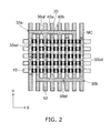
- FIG. 2 is a transparent plan view schematically showing one example of the memory cell array 1 as viewed from the upper side.
- FIG. 2 shows an arrangement of word lines 30 with respect to local bit lines 20 .
- global bit lines 10 are provided parallel and are arranged to be aligned in the Y-direction.
- the local bit lines 20 are disposed on one global bit line 10 to be aligned in the X-direction.
- the local bit lines 20 are arranged so as to be aligned also in the Y-direction. That is, the local bit lines 20 are provided with a matrix arrangement on the global bit lines 10 .
- the word line 30 shown in FIG. 2 has a comb structure that includes extending portions 30 d and a common portion 30 f . Each extending portion extends in the Y-direction between local bit lines 20 adjacent in the X-direction, and the common portion 30 f puts the extending portions 30 d together. A pair of word lines 30 a and 30 b is provided in one layer of vertical stacking structure of the word lines 30 .
- the word lines 30 are respectively referred to as the word line 30 a and 30 b . Also for other components, there are a case where components of the same kind are distinguished by being marked with different reference numerals and a case where components of the same kind are collectively referred to as a representative reference numeral.
- the word line 30 a has a first comb structure that includes first extending portions 30 ad and a first common portion 30 af
- the word line 30 b has a second comb structure that includes second extending portions 30 bd and a second common portion 30 bf .
- the extending portions 30 ad and 30 bd are respectively disposed in every other position in the X-direction. In the X-direction, the first extending portion 30 ad is disposed on one side of each local bit line 20 , and the second extending portion 30 bd is disposed on the other side thereof, facing each other across the local bit line 20 .
- first extending portions 30 ad is called “word line 30 a ”
- first extending portions 30 bd is called “word line 30 b ”.
- the pair of the word lines 30 a and 30 b face each other across the local bit line 20 .
- a first memory layer 40 a is provided between the word line 30 a and the local bit line 20 .
- a second memory layer 40 b is provided between the word line 30 b and the local bit line 20 .
- each memory cell MC is provided in each portion where the local bit line 20 and the word line 30 cross each other. That is, each memory cell MC includes either one of the first memory layer 40 a and the second memory layer 40 b.
- the gate electrode 53 of the select element 50 extends in the Y-direction below the word line 30 .
- the gate electrode 53 extends in the Y-direction between conductive portion 51 connected to the local bit line 20 , crossing the global bit line 10 .
- FIG. 3 is a block diagram showing the non-volatile memory device 100 according to the first embodiment.
- the non-volatile memory device 100 includes a row decoder 15 and a sense amplifier 17 that drive the memory cell array 1 , for example.
- the sense amplifier 17 reads out data from the memory cell MC and stores them temporally.
- the non-volatile memory device 100 further includes a control circuit 13 and an interface circuit 19 .
- the control circuit 13 receives commands from the outside via the interface circuit 19 , and based on the command, records data in the memory cell array 1 via the row decoder 15 and reads out data via the sense amplifier 17 from the memory cell array 1 .
- the control circuit 13 selects one of the global bit lines 10 via the sense amplifier 17 , for example.
- the control circuit 13 selects one of the local bit lines 20 provided on the selected global bit line 10 via the row decoder 15 .
- a gate bias is applied to the gate electrode 53 of the select element 50 provided between the selected global bit line 10 and the local bit line 20 in order to select the local bit line 20 , and the selected global bit line 10 and the local bit line 20 are electrically connected to each other.
- the control circuit 13 can select one of the word lines 30 , and thereby select one of the memory cells MCs provided between the selected local bit line 20 and the word line 30 . Specifically, either the word line 30 a or 30 b is selected at the stage where the selected memory cell MC is located.
- the control circuit 13 When reading out data stored in the memory cell MC, the control circuit 13 applies a voltage to the selected word line 30 , and detects the current flowing through the selected global bit line 10 with the sense amplifier 17 , for example. Then, data stored in the memory cell MC is specified based on the output from the sense amplifier 17 , and outputted via the interface circuit 19 .
- a prescribed voltage is applied to the selected memory cell MC via the word line 30 to make transition from the first state to the second state and vice versa.
- FIG. 4 is a cross-sectional view schematically showing one example of the memory cell array 1 according to the first embodiment.
- FIG. 4 shows a cross section taken along line A-A shown in FIG. 2 .
- the select element 50 is provided on the global bit line 10 .
- the select element 50 includes the conductive portion 51 , the gate electrode 53 facing the side surface of the conductive portion 51 , and the gate insulating film 55 provided between the conductive portion 51 and the gate electrode 53 .
- the conductive portion 51 includes a channel portion 57 , a source drain portion 58 provided on a lower side thereof and a source drain portion 59 provided on an upper side thereof.
- the channel portion 57 faces the gate electrode 53 via the gate insulating film 55 .
- the source drain portion 58 is connected to the global bit line 10 .
- the source drain portion 59 is connected to the local bit line 20 .
- An insulating layer 61 is provided between the global bit line 10 and the gate electrode 53 .
- An insulating layer 63 is provided on the gate electrode 53 .
- a silicon oxide film may be used for the insulating layers 61 and 63 , for example.
- the local bit line 20 and the word lines 30 are provided on the select element 50 .
- the word lines 30 are stacked in the Z-direction via an insulating layer 33 .
- the word line 30 a and the word line 30 b are provided alternately in the X-direction between local bit lines 20 adjacent to each other.
- the first memory layer 40 a is provided between the local bit line 20 and the word line 30 a .
- the second memory layer 40 b is provided between the local bit line 20 and the word line 30 b.
- the local bit line 20 has a first portion 21 in contact with the first memory layer 40 a and a second portion 23 in contact with the second memory layer 40 b , and includes a block portion 25 therebetween.
- FIGS. 5A and 5B are schematic diagrams showing a memory cell array 2 according to a comparative example.
- FIG. 5A is a partial cross-sectional view of the memory cell array 2
- FIG. 5B is an energy band diagram in the cross section.
- the block portion 25 is not provided in the memory cell array 2 .
- a memory cell MC 1 including the first memory layer 40 a is provided between the local bit line 20 and the word line 30 a .
- a memory cell MC 2 including the second memory layer 40 b is provided between the local bit line 20 and the word line 30 b.
- the control circuit 13 applies different voltages respectively to the word lines 30 a and 30 b facing each other across the local bit line 20 .
- the electric potential of the local bit line 20 is set to 3 V
- the electric potential of the word line 30 a is set to 2 V
- the electric potential of the word line 30 b is set to 1 V, for example. That is, a potential difference of 1 V is given to the memory cell MC 1 , and a potential difference of 2 V is given to the memory cell MC 2 .
- the thickness of the memory layer 40 is several nanometers, for example, and a strong electric field of the order of 10 6 V/cm is applied to the memory layer 40 .
- a reset current I R flows through MC 2 , and makes the transition in the second memory layer 40 b from the second state (low resistance) to the first state (high resistance), for example.
- the half voltage thereof is applied to the MC 1 , and the current flowing through the first memory layer 40 a is smaller than the reset current I R . Therefore, the resistance state of the first memory layer 40 a may not be changed.
- FIG. 5B shows an energy band diagram when the potential difference applied between the local bit line 20 and the word line 30 a is set to 1 V and the potential difference applied between the local bit line 20 and the word line 30 b is set to 2 V.
- the horizontal line Ec in FIG. 5B shows the energy level of the conduction band in the local bit line 20 and the word lines 30 a and 30 b.
- the local bit line 20 in the X-direction may be narrowed, for example, to 40 nm or less, some electrons may pass through the local bit line 20 without being scattered and flow into the memory cell MC 1 . These electrons e B may cause unintentional transition of the resistance state in the first memory layer 40 a , and change the data stored in the memory cell MC 1 . Such a phenomenon may occur with higher probability as the width of the local bit line 20 becomes narrower. Thus, the phenomenon called “disturb” between memory cells may reduce the reliability of the non-volatile memory device.
- the block portion 25 is provided in the local bit line 20 to suppress the movement of carries (electrons or holes) between the memory cell MC 1 and the memory cell MC 2 . Thereby, it is possible to improve the reliability in the non-volatile memory device 100 .
- FIGS. 6A and 6B are schematic diagrams showing one example of the memory cell array 1 according to the first embodiment.
- FIG. 6A is a partial cross-sectional view of the memory cell array 1 , and shows an example of the block portion 25 provided in the local bit line 20 .
- FIG. 6B is a schematic energy band diagram modulated by the block portion 25 shown in FIG. 6A .
- the block portion 25 of this example includes an interface 43 where the first portion 21 and the second portion 23 are in contact. That is, the block portion 25 is provided around the interface 43 , which is so called a seam.
- the interface 43 may induce a local bending E B of the energy band.
- a carrier trap E T trap center or the like may be generated at the interface 43 .
- the movement of the electrons e B in the X-direction may be blocked by a potential barrier due to the energy band bending E B , or by trapping in the carrier trap E T formed at the interface 43 .
- a density of the carrier traps E T formed at the interface 43 may become higher than that of scattering centers in the first portion 21 and the second portion 23 , and effectively suppress electrons e B flowing into the first memory layer 40 a , for example. Thereby, it is possible to suppress the malfunction of the memory cell MC 1 .
- the first portion 21 and the second portion 23 may contain a semiconductor material such as polysilicon, for example.
- the interface 43 forms a discontinuous surface of a semiconductor crystal, where the first portion 21 and the second portion 23 are in contact, and includes carrier traps E T at high density.
- FIGS. 7 to 11C are schematic views showing one example of the manufacturing process of the memory cell array according to the embodiment.
- FIGS. 7 , 8 B, 9 A to 10 B, 11 B and 11 C are partial cross-sectional views of a wafer.
- FIG. 8A and FIG. 11A are plan views showing the upper surface of the wafer.
- a wafer is prepared, in which the select element 50 is formed on the global bit line 10 .
- the wafer may include peripheral circuits such as the control circuit 13 , the row decoder 15 , and the sense amplifier 17 .
- the global bit line 10 is formed on a silicon substrate via an interlayer insulating film, for example. Then, the select element 50 is formed on the global bit line 10 .
- the stacked body 60 includes insulating layers 33 and conductive layers 31 .
- the insulating layer 33 is a silicon oxide film formed using the CVD (chemical vapor deposition) method, for example.
- the conductive layer 31 is a polysilicon film formed using the CVD method, for example.
- the insulating layer 33 and the conductive layer 31 are alternately stacked in the Z-direction.
- the stacked body 60 is selectively etched in order to form slits 65 .
- the stacked body 60 is etched using the RIE (reactive ion etching) method, for example.
- An etching mask (not-shown) is provided on the stacked body 60 .
- the slit 65 is formed so as to extend in the Y-direction.
- the slit 65 is formed with a depth reaching the select element 50 from the upper surface of the stacked body 60 .
- the source drain portion 59 of the conductive unit 51 is exposed at the bottom surface of the slit 65 .
- the memory layer 40 is formed on the inner surface of the slit 65 .
- the memory layer 40 contains a resistance change material, which is formed using the ALD (atomic layer deposition) method, for example.
- the thickness of the memory layer 40 is several nanometers, for example.
- the memory layer 40 formed on the bottom surface of the slit 65 is selectively removed to expose the source drain portion 59 .
- anisotropic etching conditions of RIE the memory layer 40 formed on the bottom surface of the slit 65 can be selectively removed, leaving the memory layer 40 on the sidewall of the slit 65 , for example.
- a conductive layer 67 is formed on the inner surface of the slit 65 .
- the conductive layer 67 may be a metal film or a polysilicon film, for example.
- an isotropic growth method such as the ALD method and the CVD method, is preferably used.
- the conductive layer 67 is deposited in the horizontal direction (the X-direction and the ⁇ X-direction) on the memory layer 40 provided on the sidewall of the slit 65 .
- a homogeneous conductive layer 67 with a uniform thickness may be formed on the sidewall of the slit 65 .
- the conductive layer 67 may bury the space of the slit 65 as shown in FIG. 10B .
- the conductive layers 67 deposited on both sidewalls of the slit 65 may be joined together at the center of the slit 65 , and a joining surface (so-called seam) or a crystalline discontinuous surface is formed so as to extend in the Z-direction.
- a joining surface so-called seam
- the potential barrier due to the energy band bending may block the movement of electrons in the X-direction.
- the seam or the discontinuous surface may include crystal defects at high density, each of which serves mainly as a carrier trap.
- the conductive layer 67 is selectively etched, and divided into the local bit lines 20 .
- insulators 38 are provided between the conductive layers 67 extending in the Y-direction, and isolate therebetween, forming local bit lines 20 . Specifically, in the portion where the insulator 38 will be formed, the conductive layer 67 is etched to a depth reaching the insulating layer 63 from the upper surface of the conductive layer 67 . The insulating layer 63 is provided so as to fill the space between select elements 50 adjacent in the Y-direction.
- the conductive layer 67 is removed so as to leave the portion in communication with the source drain portion 59 of the select element 50 . Subsequently, a silicon oxide film, for example, is buried in the space so as to form the insulator 38 , where the conductive layer 67 is removed.
- the interface 43 is formed in the local bit line 20 . As shown in FIGS. 11A and 11B , the interface 43 extends in the Y-direction and the Z-direction, and divides the local bit line 20 into the first portion 21 and the second portion 23 .
- the local bit line 20 includes part of the conductive layer 67 deposited on the source drain portion 59 , in a portion in contact with the source drain portion 59 . Therefore, the interface 43 does not extend to the end 20 e of the local bit line 20 on the global bit line 10 side.
- the end 43 e of the interface 43 be located below the word line 30 e formed in a position nearest to the global bit line 10 . It is possible to form the insulating layer 33 e on the select element 50 , which is thicker than the conductive layer 67 disposed on the source drain portion 59 .
- the spacing (W B ) between the end 25 e of the block portion 25 on the global bit line 10 side and the end 20 e of the local bit line 20 may be preferably provided to be narrower than the spacing (W L2 ) between the word line 30 e nearest to the global bit line 10 among the word lines 30 and the end 20 e of the local bit line 20 .
- the film thickness of the lowermost insulating film 30 eb may be thicker than the film thickness of the other insulating films 33 e . That is, as the width of the slit 65 becomes narrower, the spacing WB becomes larger. However, if a thickness of all the insulating films 30 e is thick, the height of the slit 65 becomes too high. Hence, it is preferable to form the film thickness of the lowermost insulating film 30 eb thicker than the other insulating film 30 , so that the spacing W L2 is made larger than W L (W L ⁇ W L2 ). Thus, the relationship of spacing W B ⁇ spacing W L2 can be maintained even when the width of the slit 65 is narrow.
- the spacing between the lower surface of the word line 30 e and the end 20 e of the local bit line 20 is wider than the spacing between two word lines 30 adjacent in the Z-direction among the word lines 30 stacked in the Z-direction.
- FIG. 12 is a schematic cross-sectional view showing one example of a memory cell array 3 according to a variation of the first embodiment.
- the block portion 25 includes a block layer 45 provided between the first portion 21 and the second portion 23 .
- the first portion 21 and the second portion 23 specifically contain a first metal.
- the block layer 45 contains a second metal having a smaller work function than the first metal.
- the first metal is tantalum nitride (TaN), for example, and the second metal is tungsten (W), for example.
- Electrons e B that are injected into the local bit line 20 from the word line 30 b through the second memory layer 40 b can be prevented from flowing into the first memory layer 40 a , for example. Electrons that flow from the word line 30 a through the first memory layer 40 a into the local bit line 20 may be also prevented from being injected into the second memory layer 40 a.
- the first portion 21 and the second portion 23 may contain a first semiconductor
- the block layer 45 may contain a second semiconductor having a wider band gap than the first semiconductor.
- silicon may be used as the first semiconductor
- gallium arsenide (GaAs) or gallium nitride (GaN) may be used as the second semiconductor. That is, the discontinuity of the energy band between the first semiconductor and the second semiconductor forms a potential barrier, and may block the movement of carries in the X-direction in the local bit line 20 .
- FIGS. 13A to 13C are schematic diagrams showing a memory cell array 4 according to another variation of the first embodiment.
- FIG. 13A is a partial cross-sectional view showing the memory cell array 4 .
- FIGS. 13B and 13C show impurity profiles of the local bit line 20 .
- the local bit line 20 contains a semiconductor.
- the impurity concentration of the block portion 25 is lower than the impurity concentration of the first portion 21 .
- the impurity concentration of the block portion 25 is lower than the impurity concentration of the second portion 23 . Therefore, a potential barrier due to the concentration difference is formed between the block portion 25 and the first portion 21 , and also between the block portion 25 and the second portion. Then, the block portion 25 may suppress the movement of carriers in the X-direction in the local bit line 20 .
- the impurity distribution in the local bit line 20 is formed so as to continuously decrease from the first memory layer 40 a side or the second memory layer 40 b side toward the center. That is, while depositing the conductive layer 67 (see FIGS. 10A and 10B ), the doping amount of the impurity is set large in a first half of the deposition time, and is set small in the second half thereof, for example.
- the impurity distribution in the local bit line 20 may be formed so as to decrease in a step form at a boundary between the first portion 21 and the block portion 25 , and at another boundary between the second portion 23 and the block portion 25 .
- the local bit line 20 contains polysilicon, for example.
- the impurity doped into the local bit line 20 is arsenic (As), phosphorus (P), or boron (B), for example.
- FIG. 14 is a cross-sectional view schematically showing one example of a memory cell array 5 according to a second embodiment.
- the local bit line 20 has a gap 47 between the first portion 21 in contact with the first memory layer 40 a and the second portion 23 in contact with the second memory layer 40 b .
- the deposition is suspended, for example. Thereby, a space can be formed between the first portion 21 and the second portion 23 .
- the gap 47 extends in the Z-direction in the local bit line 20 .
- the gap 47 may block the movement of carries that flow from one of the word lines 30 a and 30 b through the memory layer 40 into the local bit line 20 , preventing the carrier from moving toward the other of the word lines 30 a and 30 b . Thereby, the “disturb” can be suppressed between memory cells facing each other across the local bit line 20 .
- the spacing W B is narrower than the spacing W L .
- the spacing W B is the one between the end 47 e of the gap 47 on the global bit line 10 side and the end 20 e of the local bit line on the global bit line 10 side.
- the spacing W L is the one between the word line 30 e nearest to the global bit line 10 out of the plurality of word lines 30 and the end 20 e of the local bit line 20 .
- the “disturb” can be suppressed between the memory cells MC 3 and MC 4 formed in a position nearest to the global bit line 10 .
- the film thickness of the lowermost insulating film 30 eb may be thicker than the film thickness of the other insulating films 33 e . That is, when the width of the slit 65 becomes narrower, the spacing W B becomes larger. However, if a thickness of all the insulating films 30 e is thick, the height of the slit 65 becomes too high. Thus, by forming the film thickness of the lowermost insulating film 30 eb thicker, the spacing W L2 is made larger (W L ⁇ W L2 ). Therefore, the relationship of spacing W B ⁇ spacing W L2 can be maintained even when the width of the slit 65 is narrow.
- the spacing between the lower surface of the word line 30 e and the end 20 e of the local bit line 20 is wider than the spacing between two word lines 30 adjacent in the Z-direction among the word lines 30 stacked in the Z-direction.
- FIG. 15 is a schematic cross-sectional view showing one example of a memory cell array 6 of a non-volatile memory device 200 according to a third embodiment.
- the non-volatile memory device 200 is called a vertical cross-point structure, and the local bit line 20 is directly connected to the global bit line 10 .
- a rectifying element for example, a diode is provided between the local bit line 20 and the word line 30 .
- the local bit line 20 is directly connected to the global bit line 10 .
- Word lines 30 are aligned on both sides of the local bit line 20 .
- a word line 30 disposed between local bit lines 20 adjacent in the X-direction faces one of the local bit lines 20 via the memory layer 40 .
- the memory layer 40 includes a resistance change layer 42 provided on the word line 30 side and a rectifying layer 71 in contact with the local bit line 20 .
- the word line 30 a and the word line 30 b shown in FIG. 15 face each other across the local bit line 20 in the X-direction.
- the first memory layer 40 a is provided between the local bit line 20 and the word line 30 a .
- the second memory layer 40 b is provided between the local bit line 20 and the word line 30 b.
- the first memory layer 40 a includes a first rectifying layer 71 a in a portion in contact with the local bit line 20 .
- the second memory layer 40 b includes a second rectifying layer 71 b in a portion in contact with the local bit line 20 .
- the first rectifying layer 71 a interposes a first diode between the first memory layer 40 a and the local bit line 20 .
- the second rectifying layer 71 b interposes a second diode between the second memory layer 40 b and the local bit line 20 .
- the rectifying layer 71 contains a semiconductor, for example. Thereby, a Schottky diode can be interposed between the local bit line 20 and the memory layer 40 .
- the rectifying layer 71 contains a semiconductor of a different conductivity type from the local bit line 20 .
- a P-N junction diode can be interposed between the local bit line 20 and the memory layer 40 .
- the local bit line 20 has the first portion 21 in contact with the first memory layer 40 a and the second portion 23 in contact with the second memory layer 40 b , and includes the block portion 25 between them.
- the block portion 25 block the movement of carriers that flow from one of the word lines 30 a and 30 b through the memory layer 40 into the local bit line 20 , and preventing the carriers from moving toward the other of the word lines 30 a and 30 b . Thereby, the “disturb” can be suppressed between memory cells facing each other across the local bit line 20 .
- the block portion 25 may have the same structure as the first embodiment. It is possible to provide the gap 47 between the first portion 21 and the second portion 23 .
Abstract
Description
Claims (16)
Priority Applications (2)
| Application Number | Priority Date | Filing Date | Title |
|---|---|---|---|
| US14/107,442 US9281345B2 (en) | 2013-07-09 | 2013-12-16 | Resistance change type memory device with three-dimensional structure |
| JP2014065806A JP2015019048A (en) | 2013-07-09 | 2014-03-27 | Non-volatile memory device |
Applications Claiming Priority (2)
| Application Number | Priority Date | Filing Date | Title |
|---|---|---|---|
| US201361844234P | 2013-07-09 | 2013-07-09 | |
| US14/107,442 US9281345B2 (en) | 2013-07-09 | 2013-12-16 | Resistance change type memory device with three-dimensional structure |
Publications (2)
| Publication Number | Publication Date |
|---|---|
| US20150014622A1 US20150014622A1 (en) | 2015-01-15 |
| US9281345B2 true US9281345B2 (en) | 2016-03-08 |
Family
ID=52257438
Family Applications (1)
| Application Number | Title | Priority Date | Filing Date |
|---|---|---|---|
| US14/107,442 Active 2034-02-21 US9281345B2 (en) | 2013-07-09 | 2013-12-16 | Resistance change type memory device with three-dimensional structure |
Country Status (4)
| Country | Link |
|---|---|
| US (1) | US9281345B2 (en) |
| JP (1) | JP2015019048A (en) |
| CN (1) | CN104282709B (en) |
| TW (1) | TWI546902B (en) |
Cited By (4)
| Publication number | Priority date | Publication date | Assignee | Title |
|---|---|---|---|---|
| US10050087B1 (en) | 2017-03-16 | 2018-08-14 | Toshiba Memory Corporation | Semiconductor memory device |
| US10096652B2 (en) | 2016-09-12 | 2018-10-09 | Toshiba Memory Corporation | Semiconductor memory device |
| US10256401B2 (en) | 2017-03-17 | 2019-04-09 | Toshiba Memory Corporation | Memory device with multiple interconnect lines |
| US10319786B2 (en) | 2017-09-19 | 2019-06-11 | Toshiba Memory Corporation | Memory device |
Families Citing this family (11)
| Publication number | Priority date | Publication date | Assignee | Title |
|---|---|---|---|---|
| US9721961B2 (en) | 2015-05-29 | 2017-08-01 | Kabushiki Kaisha Toshiba | Semiconductor memory device |
| US9704922B2 (en) | 2015-05-29 | 2017-07-11 | Kabushiki Kaisha Toshiba | Semiconductor memory device and method of manufacturing the same while avoiding process damage to a variable resistance film |
| US9825100B2 (en) | 2015-08-31 | 2017-11-21 | Toshiba Memory Corporation | Nonvolatile semiconductor memory device |
| US9748312B2 (en) | 2015-10-29 | 2017-08-29 | Kabushiki Kaisha Toshiba | Semiconductor memory device |
| US9865656B2 (en) | 2016-02-12 | 2018-01-09 | Toshiba Memory Corporation | Semiconductor memory device |
| TWI624007B (en) * | 2016-04-25 | 2018-05-11 | 東芝記憶體股份有限公司 | Semiconductor memory device and method for manufacturing same |
| US10134755B2 (en) | 2016-09-16 | 2018-11-20 | Toshiba Memory Corporation | Semiconductor memory device |
| JP2019053804A (en) * | 2017-09-15 | 2019-04-04 | 東芝メモリ株式会社 | Semiconductor storage device |
| JP2020043189A (en) * | 2018-09-10 | 2020-03-19 | キオクシア株式会社 | Semiconductor storage device |
| JP2021048159A (en) * | 2019-09-17 | 2021-03-25 | キオクシア株式会社 | Semiconductor storage device |
| JP2022553435A (en) * | 2019-12-18 | 2022-12-22 | マイクロン テクノロジー,インク. | Vertical 3D memory device and method for manufacturing same |
Citations (9)
| Publication number | Priority date | Publication date | Assignee | Title |
|---|---|---|---|---|
| US5565708A (en) * | 1994-10-06 | 1996-10-15 | Mitsubishi Denki Kabushiki Kaisha | Semiconductor device comprising composite barrier layer |
| US6611010B2 (en) | 1999-12-03 | 2003-08-26 | Kabushiki Kaisha Toshiba | Semiconductor device |
| US7205590B2 (en) * | 2004-03-18 | 2007-04-17 | Kabushiki Kaisha Toshiba | Semiconductor memory device provided with magneto-resistive element and method for fabricating the same |
| US7227171B2 (en) * | 2001-12-05 | 2007-06-05 | Stmicroelectronics S.R.L. | Small area contact region, high efficiency phase change memory cell and fabrication method thereof |
| US20100219392A1 (en) * | 2009-02-27 | 2010-09-02 | Nobuyoshi Awaya | Nonvolatile semiconductor memory device and manufacturing method for same |
| US20110149656A1 (en) | 2009-12-23 | 2011-06-23 | Tang Sanh D | Multi-cell vertical memory nodes |
| TW201209827A (en) | 2010-06-08 | 2012-03-01 | Sandisk 3D Llc | Non-volatile memory having 3D array of read/write elements with vertical bit lines and laterally aligned active elements and methods thereof |
| US20120112156A1 (en) | 2010-11-10 | 2012-05-10 | Heung-Kyu Park | Non-Volatile Memory Devices Having Resistance Changeable Elements And Related Systems And Methods |
| US8357613B2 (en) | 2009-02-12 | 2013-01-22 | Samsung Electronics Co., Ltd. | Methods of fabricating semiconductor devices and semiconductor devices including a contact plug processed by rapid thermal annealing |
Family Cites Families (3)
| Publication number | Priority date | Publication date | Assignee | Title |
|---|---|---|---|---|
| US7034332B2 (en) * | 2004-01-27 | 2006-04-25 | Hewlett-Packard Development Company, L.P. | Nanometer-scale memory device utilizing self-aligned rectifying elements and method of making |
| KR101322747B1 (en) * | 2005-03-25 | 2013-11-04 | 가부시키가이샤 한도오따이 에네루기 켄큐쇼 | Semiconductor device and electronic appliance |
| KR20110040461A (en) * | 2009-10-14 | 2011-04-20 | 삼성전자주식회사 | Nonvolatile memory device and method of manufacturing the same |
-
2013
- 2013-12-16 US US14/107,442 patent/US9281345B2/en active Active
- 2013-12-18 TW TW102146998A patent/TWI546902B/en active
- 2013-12-27 CN CN201310741526.0A patent/CN104282709B/en active Active
-
2014
- 2014-03-27 JP JP2014065806A patent/JP2015019048A/en active Pending
Patent Citations (10)
| Publication number | Priority date | Publication date | Assignee | Title |
|---|---|---|---|---|
| US5565708A (en) * | 1994-10-06 | 1996-10-15 | Mitsubishi Denki Kabushiki Kaisha | Semiconductor device comprising composite barrier layer |
| US6611010B2 (en) | 1999-12-03 | 2003-08-26 | Kabushiki Kaisha Toshiba | Semiconductor device |
| US7227171B2 (en) * | 2001-12-05 | 2007-06-05 | Stmicroelectronics S.R.L. | Small area contact region, high efficiency phase change memory cell and fabrication method thereof |
| US7205590B2 (en) * | 2004-03-18 | 2007-04-17 | Kabushiki Kaisha Toshiba | Semiconductor memory device provided with magneto-resistive element and method for fabricating the same |
| US8357613B2 (en) | 2009-02-12 | 2013-01-22 | Samsung Electronics Co., Ltd. | Methods of fabricating semiconductor devices and semiconductor devices including a contact plug processed by rapid thermal annealing |
| US20100219392A1 (en) * | 2009-02-27 | 2010-09-02 | Nobuyoshi Awaya | Nonvolatile semiconductor memory device and manufacturing method for same |
| US8450713B2 (en) | 2009-02-27 | 2013-05-28 | Sharp Kabushiki Kaisha | Nonvolatile semiconductor memory device and manufacturing method for same |
| US20110149656A1 (en) | 2009-12-23 | 2011-06-23 | Tang Sanh D | Multi-cell vertical memory nodes |
| TW201209827A (en) | 2010-06-08 | 2012-03-01 | Sandisk 3D Llc | Non-volatile memory having 3D array of read/write elements with vertical bit lines and laterally aligned active elements and methods thereof |
| US20120112156A1 (en) | 2010-11-10 | 2012-05-10 | Heung-Kyu Park | Non-Volatile Memory Devices Having Resistance Changeable Elements And Related Systems And Methods |
Non-Patent Citations (1)
| Title |
|---|
| Office Action issued Jul. 15, 2015 in Taiwanese Patent Application No. 102146998 (with English language translation). |
Cited By (4)
| Publication number | Priority date | Publication date | Assignee | Title |
|---|---|---|---|---|
| US10096652B2 (en) | 2016-09-12 | 2018-10-09 | Toshiba Memory Corporation | Semiconductor memory device |
| US10050087B1 (en) | 2017-03-16 | 2018-08-14 | Toshiba Memory Corporation | Semiconductor memory device |
| US10256401B2 (en) | 2017-03-17 | 2019-04-09 | Toshiba Memory Corporation | Memory device with multiple interconnect lines |
| US10319786B2 (en) | 2017-09-19 | 2019-06-11 | Toshiba Memory Corporation | Memory device |
Also Published As
| Publication number | Publication date |
|---|---|
| TW201503290A (en) | 2015-01-16 |
| US20150014622A1 (en) | 2015-01-15 |
| CN104282709B (en) | 2017-06-16 |
| TWI546902B (en) | 2016-08-21 |
| CN104282709A (en) | 2015-01-14 |
| JP2015019048A (en) | 2015-01-29 |
Similar Documents
| Publication | Publication Date | Title |
|---|---|---|
| US9281345B2 (en) | Resistance change type memory device with three-dimensional structure | |
| Yoon et al. | Highly uniform, electroforming‐free, and self‐rectifying resistive memory in the Pt/Ta2O5/HfO2‐x/TiN structure | |
| US9698202B2 (en) | Parallel bit line three-dimensional resistive random access memory | |
| US9818801B1 (en) | Resistive three-dimensional memory device with heterostructure semiconductor local bit line and method of making thereof | |
| US8431923B2 (en) | Semiconductor structure and semiconductor device including a diode structure and methods of forming same | |
| SG194300A1 (en) | Non-volatile memory device and method of forming the same | |
| US9704920B2 (en) | Resistive random access memory containing a steering element and a tunneling dielectric element | |
| US9865809B2 (en) | Nonvolatile resistance change element | |
| US20160276353A1 (en) | Nonvolatile semiconductor memory device | |
| US9450026B2 (en) | Semiconductor device | |
| JP2010087259A (en) | Method of manufacturing nonvolatile storage device | |
| US9570514B2 (en) | Semiconductor device | |
| US9680096B2 (en) | Tunable voltage margin access diodes | |
| US20150076438A1 (en) | Non-volatile resistive memory cells | |
| US10128310B2 (en) | Magnetoresistive memory device and manufacturing method of the same | |
| US20220344510A1 (en) | Transistor including an active region and methods for forming the same | |
| US11538919B2 (en) | Transistors and arrays of elevationally-extending strings of memory cells | |
| US20230079445A1 (en) | Memory device | |
| EP4152328A1 (en) | Memory device | |
| US11856766B2 (en) | Memory cell having programmable material comprising at least two regions comprising SiNx | |
| US20220271127A1 (en) | Transistors And Arrays Of Elevationally-Extending Strings Of Memory Cells | |
| US10651300B2 (en) | Charge storage and sensing devices and methods | |
| US20220069205A1 (en) | Switching device having bi-directional drive characteristics and method of operating same | |
| US9871197B2 (en) | Semiconductor memory device | |
| TW202238735A (en) | Semiconductor device and methods for forming the same |
Legal Events
| Date | Code | Title | Description |
|---|---|---|---|
| AS | Assignment |
Owner name: KABUSHIKI KAISHA TOSHIBA, JAPAN Free format text: ASSIGNMENT OF ASSIGNORS INTEREST;ASSIGNORS:KANNO, HIROSHI;MINEMURA, YOICHI;TSUKAMOTO, TAKAYUKI;AND OTHERS;REEL/FRAME:031790/0664 Effective date: 20131128 |
|
| STCF | Information on status: patent grant |
Free format text: PATENTED CASE |
|
| AS | Assignment |
Owner name: TOSHIBA MEMORY CORPORATION, JAPAN Free format text: ASSIGNMENT OF ASSIGNORS INTEREST;ASSIGNOR:KABUSHIKI KAISHA TOSHIBA;REEL/FRAME:043709/0035 Effective date: 20170706 |
|
| MAFP | Maintenance fee payment |
Free format text: PAYMENT OF MAINTENANCE FEE, 4TH YEAR, LARGE ENTITY (ORIGINAL EVENT CODE: M1551); ENTITY STATUS OF PATENT OWNER: LARGE ENTITY Year of fee payment: 4 |
|
| AS | Assignment |
Owner name: K.K. PANGEA, JAPAN Free format text: MERGER;ASSIGNOR:TOSHIBA MEMORY CORPORATION;REEL/FRAME:055659/0471 Effective date: 20180801 Owner name: TOSHIBA MEMORY CORPORATION, JAPAN Free format text: CHANGE OF NAME AND ADDRESS;ASSIGNOR:K.K. PANGEA;REEL/FRAME:055669/0401 Effective date: 20180801 Owner name: KIOXIA CORPORATION, JAPAN Free format text: CHANGE OF NAME AND ADDRESS;ASSIGNOR:TOSHIBA MEMORY CORPORATION;REEL/FRAME:055669/0001 Effective date: 20191001 |
|
| MAFP | Maintenance fee payment |
Free format text: PAYMENT OF MAINTENANCE FEE, 8TH YEAR, LARGE ENTITY (ORIGINAL EVENT CODE: M1552); ENTITY STATUS OF PATENT OWNER: LARGE ENTITY Year of fee payment: 8 |