US9293423B2 - Workpiece with semiconductor chips, semiconductor device and method for producing a workpiece with semiconductor chips - Google Patents
Workpiece with semiconductor chips, semiconductor device and method for producing a workpiece with semiconductor chips Download PDFInfo
- Publication number
- US9293423B2 US9293423B2 US14/330,066 US201414330066A US9293423B2 US 9293423 B2 US9293423 B2 US 9293423B2 US 201414330066 A US201414330066 A US 201414330066A US 9293423 B2 US9293423 B2 US 9293423B2
- Authority
- US
- United States
- Prior art keywords
- main surface
- layer
- semiconductor device
- electrically conducting
- semiconductor chip
- Prior art date
- Legal status (The legal status is an assumption and is not a legal conclusion. Google has not performed a legal analysis and makes no representation as to the accuracy of the status listed.)
- Active
Links
Images


Classifications
-
- H—ELECTRICITY
- H01—ELECTRIC ELEMENTS
- H01L—SEMICONDUCTOR DEVICES NOT COVERED BY CLASS H10
- H01L21/00—Processes or apparatus adapted for the manufacture or treatment of semiconductor or solid state devices or of parts thereof
- H01L21/02—Manufacture or treatment of semiconductor devices or of parts thereof
- H01L21/04—Manufacture or treatment of semiconductor devices or of parts thereof the devices having at least one potential-jump barrier or surface barrier, e.g. PN junction, depletion layer or carrier concentration layer
- H01L21/50—Assembly of semiconductor devices using processes or apparatus not provided for in a single one of the subgroups H01L21/06 - H01L21/326, e.g. sealing of a cap to a base of a container
- H01L21/56—Encapsulations, e.g. encapsulation layers, coatings
- H01L21/561—Batch processing
-
- H—ELECTRICITY
- H01—ELECTRIC ELEMENTS
- H01L—SEMICONDUCTOR DEVICES NOT COVERED BY CLASS H10
- H01L23/00—Details of semiconductor or other solid state devices
- H01L23/58—Structural electrical arrangements for semiconductor devices not otherwise provided for, e.g. in combination with batteries
- H01L23/60—Protection against electrostatic charges or discharges, e.g. Faraday shields
-
- H—ELECTRICITY
- H01—ELECTRIC ELEMENTS
- H01L—SEMICONDUCTOR DEVICES NOT COVERED BY CLASS H10
- H01L25/00—Assemblies consisting of a plurality of individual semiconductor or other solid state devices ; Multistep manufacturing processes thereof
- H01L25/50—Multistep manufacturing processes of assemblies consisting of devices, each device being of a type provided for in group H01L27/00 or H01L29/00
-
- H—ELECTRICITY
- H01—ELECTRIC ELEMENTS
- H01L—SEMICONDUCTOR DEVICES NOT COVERED BY CLASS H10
- H01L21/00—Processes or apparatus adapted for the manufacture or treatment of semiconductor or solid state devices or of parts thereof
- H01L21/02—Manufacture or treatment of semiconductor devices or of parts thereof
- H01L21/04—Manufacture or treatment of semiconductor devices or of parts thereof the devices having at least one potential-jump barrier or surface barrier, e.g. PN junction, depletion layer or carrier concentration layer
- H01L21/48—Manufacture or treatment of parts, e.g. containers, prior to assembly of the devices, using processes not provided for in a single one of the subgroups H01L21/06 - H01L21/326
- H01L21/4814—Conductive parts
- H01L21/4846—Leads on or in insulating or insulated substrates, e.g. metallisation
- H01L21/4853—Connection or disconnection of other leads to or from a metallisation, e.g. pins, wires, bumps
-
- H—ELECTRICITY
- H01—ELECTRIC ELEMENTS
- H01L—SEMICONDUCTOR DEVICES NOT COVERED BY CLASS H10
- H01L21/00—Processes or apparatus adapted for the manufacture or treatment of semiconductor or solid state devices or of parts thereof
- H01L21/02—Manufacture or treatment of semiconductor devices or of parts thereof
- H01L21/04—Manufacture or treatment of semiconductor devices or of parts thereof the devices having at least one potential-jump barrier or surface barrier, e.g. PN junction, depletion layer or carrier concentration layer
- H01L21/48—Manufacture or treatment of parts, e.g. containers, prior to assembly of the devices, using processes not provided for in a single one of the subgroups H01L21/06 - H01L21/326
- H01L21/4814—Conductive parts
- H01L21/4846—Leads on or in insulating or insulated substrates, e.g. metallisation
- H01L21/486—Via connections through the substrate with or without pins
-
- H—ELECTRICITY
- H01—ELECTRIC ELEMENTS
- H01L—SEMICONDUCTOR DEVICES NOT COVERED BY CLASS H10
- H01L21/00—Processes or apparatus adapted for the manufacture or treatment of semiconductor or solid state devices or of parts thereof
- H01L21/02—Manufacture or treatment of semiconductor devices or of parts thereof
- H01L21/04—Manufacture or treatment of semiconductor devices or of parts thereof the devices having at least one potential-jump barrier or surface barrier, e.g. PN junction, depletion layer or carrier concentration layer
- H01L21/50—Assembly of semiconductor devices using processes or apparatus not provided for in a single one of the subgroups H01L21/06 - H01L21/326, e.g. sealing of a cap to a base of a container
- H01L21/56—Encapsulations, e.g. encapsulation layers, coatings
- H01L21/565—Moulds
-
- H—ELECTRICITY
- H01—ELECTRIC ELEMENTS
- H01L—SEMICONDUCTOR DEVICES NOT COVERED BY CLASS H10
- H01L21/00—Processes or apparatus adapted for the manufacture or treatment of semiconductor or solid state devices or of parts thereof
- H01L21/02—Manufacture or treatment of semiconductor devices or of parts thereof
- H01L21/04—Manufacture or treatment of semiconductor devices or of parts thereof the devices having at least one potential-jump barrier or surface barrier, e.g. PN junction, depletion layer or carrier concentration layer
- H01L21/50—Assembly of semiconductor devices using processes or apparatus not provided for in a single one of the subgroups H01L21/06 - H01L21/326, e.g. sealing of a cap to a base of a container
- H01L21/56—Encapsulations, e.g. encapsulation layers, coatings
- H01L21/568—Temporary substrate used as encapsulation process aid
-
- H—ELECTRICITY
- H01—ELECTRIC ELEMENTS
- H01L—SEMICONDUCTOR DEVICES NOT COVERED BY CLASS H10
- H01L23/00—Details of semiconductor or other solid state devices
- H01L23/28—Encapsulations, e.g. encapsulating layers, coatings, e.g. for protection
- H01L23/31—Encapsulations, e.g. encapsulating layers, coatings, e.g. for protection characterised by the arrangement or shape
- H01L23/3107—Encapsulations, e.g. encapsulating layers, coatings, e.g. for protection characterised by the arrangement or shape the device being completely enclosed
- H01L23/3121—Encapsulations, e.g. encapsulating layers, coatings, e.g. for protection characterised by the arrangement or shape the device being completely enclosed a substrate forming part of the encapsulation
- H01L23/3128—Encapsulations, e.g. encapsulating layers, coatings, e.g. for protection characterised by the arrangement or shape the device being completely enclosed a substrate forming part of the encapsulation the substrate having spherical bumps for external connection
-
- H—ELECTRICITY
- H01—ELECTRIC ELEMENTS
- H01L—SEMICONDUCTOR DEVICES NOT COVERED BY CLASS H10
- H01L23/00—Details of semiconductor or other solid state devices
- H01L23/48—Arrangements for conducting electric current to or from the solid state body in operation, e.g. leads, terminal arrangements ; Selection of materials therefor
-
- H—ELECTRICITY
- H01—ELECTRIC ELEMENTS
- H01L—SEMICONDUCTOR DEVICES NOT COVERED BY CLASS H10
- H01L23/00—Details of semiconductor or other solid state devices
- H01L23/52—Arrangements for conducting electric current within the device in operation from one component to another, i.e. interconnections, e.g. wires, lead frames
- H01L23/538—Arrangements for conducting electric current within the device in operation from one component to another, i.e. interconnections, e.g. wires, lead frames the interconnection structure between a plurality of semiconductor chips being formed on, or in, insulating substrates
- H01L23/5389—Arrangements for conducting electric current within the device in operation from one component to another, i.e. interconnections, e.g. wires, lead frames the interconnection structure between a plurality of semiconductor chips being formed on, or in, insulating substrates the chips being integrally enclosed by the interconnect and support structures
-
- H—ELECTRICITY
- H01—ELECTRIC ELEMENTS
- H01L—SEMICONDUCTOR DEVICES NOT COVERED BY CLASS H10
- H01L23/00—Details of semiconductor or other solid state devices
- H01L23/552—Protection against radiation, e.g. light or electromagnetic waves
-
- H—ELECTRICITY
- H01—ELECTRIC ELEMENTS
- H01L—SEMICONDUCTOR DEVICES NOT COVERED BY CLASS H10
- H01L24/00—Arrangements for connecting or disconnecting semiconductor or solid-state bodies; Methods or apparatus related thereto
- H01L24/01—Means for bonding being attached to, or being formed on, the surface to be connected, e.g. chip-to-package, die-attach, "first-level" interconnects; Manufacturing methods related thereto
- H01L24/18—High density interconnect [HDI] connectors; Manufacturing methods related thereto
- H01L24/19—Manufacturing methods of high density interconnect preforms
-
- H—ELECTRICITY
- H01—ELECTRIC ELEMENTS
- H01L—SEMICONDUCTOR DEVICES NOT COVERED BY CLASS H10
- H01L24/00—Arrangements for connecting or disconnecting semiconductor or solid-state bodies; Methods or apparatus related thereto
- H01L24/93—Batch processes
- H01L24/95—Batch processes at chip-level, i.e. with connecting carried out on a plurality of singulated devices, i.e. on diced chips
- H01L24/96—Batch processes at chip-level, i.e. with connecting carried out on a plurality of singulated devices, i.e. on diced chips the devices being encapsulated in a common layer, e.g. neo-wafer or pseudo-wafer, said common layer being separable into individual assemblies after connecting
-
- H—ELECTRICITY
- H01—ELECTRIC ELEMENTS
- H01L—SEMICONDUCTOR DEVICES NOT COVERED BY CLASS H10
- H01L24/00—Arrangements for connecting or disconnecting semiconductor or solid-state bodies; Methods or apparatus related thereto
- H01L24/93—Batch processes
- H01L24/95—Batch processes at chip-level, i.e. with connecting carried out on a plurality of singulated devices, i.e. on diced chips
- H01L24/97—Batch processes at chip-level, i.e. with connecting carried out on a plurality of singulated devices, i.e. on diced chips the devices being connected to a common substrate, e.g. interposer, said common substrate being separable into individual assemblies after connecting
-
- H—ELECTRICITY
- H01—ELECTRIC ELEMENTS
- H01L—SEMICONDUCTOR DEVICES NOT COVERED BY CLASS H10
- H01L2224/00—Indexing scheme for arrangements for connecting or disconnecting semiconductor or solid-state bodies and methods related thereto as covered by H01L24/00
- H01L2224/01—Means for bonding being attached to, or being formed on, the surface to be connected, e.g. chip-to-package, die-attach, "first-level" interconnects; Manufacturing methods related thereto
- H01L2224/02—Bonding areas; Manufacturing methods related thereto
- H01L2224/04—Structure, shape, material or disposition of the bonding areas prior to the connecting process
- H01L2224/0401—Bonding areas specifically adapted for bump connectors, e.g. under bump metallisation [UBM]
-
- H—ELECTRICITY
- H01—ELECTRIC ELEMENTS
- H01L—SEMICONDUCTOR DEVICES NOT COVERED BY CLASS H10
- H01L2224/00—Indexing scheme for arrangements for connecting or disconnecting semiconductor or solid-state bodies and methods related thereto as covered by H01L24/00
- H01L2224/01—Means for bonding being attached to, or being formed on, the surface to be connected, e.g. chip-to-package, die-attach, "first-level" interconnects; Manufacturing methods related thereto
- H01L2224/02—Bonding areas; Manufacturing methods related thereto
- H01L2224/04—Structure, shape, material or disposition of the bonding areas prior to the connecting process
- H01L2224/04105—Bonding areas formed on an encapsulation of the semiconductor or solid-state body, e.g. bonding areas on chip-scale packages
-
- H—ELECTRICITY
- H01—ELECTRIC ELEMENTS
- H01L—SEMICONDUCTOR DEVICES NOT COVERED BY CLASS H10
- H01L2224/00—Indexing scheme for arrangements for connecting or disconnecting semiconductor or solid-state bodies and methods related thereto as covered by H01L24/00
- H01L2224/01—Means for bonding being attached to, or being formed on, the surface to be connected, e.g. chip-to-package, die-attach, "first-level" interconnects; Manufacturing methods related thereto
- H01L2224/10—Bump connectors; Manufacturing methods related thereto
- H01L2224/12—Structure, shape, material or disposition of the bump connectors prior to the connecting process
- H01L2224/12105—Bump connectors formed on an encapsulation of the semiconductor or solid-state body, e.g. bumps on chip-scale packages
-
- H—ELECTRICITY
- H01—ELECTRIC ELEMENTS
- H01L—SEMICONDUCTOR DEVICES NOT COVERED BY CLASS H10
- H01L2224/00—Indexing scheme for arrangements for connecting or disconnecting semiconductor or solid-state bodies and methods related thereto as covered by H01L24/00
- H01L2224/01—Means for bonding being attached to, or being formed on, the surface to be connected, e.g. chip-to-package, die-attach, "first-level" interconnects; Manufacturing methods related thereto
- H01L2224/18—High density interconnect [HDI] connectors; Manufacturing methods related thereto
- H01L2224/20—Structure, shape, material or disposition of high density interconnect preforms
-
- H—ELECTRICITY
- H01—ELECTRIC ELEMENTS
- H01L—SEMICONDUCTOR DEVICES NOT COVERED BY CLASS H10
- H01L2224/00—Indexing scheme for arrangements for connecting or disconnecting semiconductor or solid-state bodies and methods related thereto as covered by H01L24/00
- H01L2224/80—Methods for connecting semiconductor or other solid state bodies using means for bonding being attached to, or being formed on, the surface to be connected
- H01L2224/82—Methods for connecting semiconductor or other solid state bodies using means for bonding being attached to, or being formed on, the surface to be connected by forming build-up interconnects at chip-level, e.g. for high density interconnects [HDI]
-
- H—ELECTRICITY
- H01—ELECTRIC ELEMENTS
- H01L—SEMICONDUCTOR DEVICES NOT COVERED BY CLASS H10
- H01L2224/00—Indexing scheme for arrangements for connecting or disconnecting semiconductor or solid-state bodies and methods related thereto as covered by H01L24/00
- H01L2224/93—Batch processes
- H01L2224/95—Batch processes at chip-level, i.e. with connecting carried out on a plurality of singulated devices, i.e. on diced chips
- H01L2224/97—Batch processes at chip-level, i.e. with connecting carried out on a plurality of singulated devices, i.e. on diced chips the devices being connected to a common substrate, e.g. interposer, said common substrate being separable into individual assemblies after connecting
-
- H—ELECTRICITY
- H01—ELECTRIC ELEMENTS
- H01L—SEMICONDUCTOR DEVICES NOT COVERED BY CLASS H10
- H01L2924/00—Indexing scheme for arrangements or methods for connecting or disconnecting semiconductor or solid-state bodies as covered by H01L24/00
-
- H—ELECTRICITY
- H01—ELECTRIC ELEMENTS
- H01L—SEMICONDUCTOR DEVICES NOT COVERED BY CLASS H10
- H01L2924/00—Indexing scheme for arrangements or methods for connecting or disconnecting semiconductor or solid-state bodies as covered by H01L24/00
- H01L2924/01—Chemical elements
- H01L2924/01006—Carbon [C]
-
- H—ELECTRICITY
- H01—ELECTRIC ELEMENTS
- H01L—SEMICONDUCTOR DEVICES NOT COVERED BY CLASS H10
- H01L2924/00—Indexing scheme for arrangements or methods for connecting or disconnecting semiconductor or solid-state bodies as covered by H01L24/00
- H01L2924/01—Chemical elements
- H01L2924/01015—Phosphorus [P]
-
- H—ELECTRICITY
- H01—ELECTRIC ELEMENTS
- H01L—SEMICONDUCTOR DEVICES NOT COVERED BY CLASS H10
- H01L2924/00—Indexing scheme for arrangements or methods for connecting or disconnecting semiconductor or solid-state bodies as covered by H01L24/00
- H01L2924/01—Chemical elements
- H01L2924/01033—Arsenic [As]
-
- H—ELECTRICITY
- H01—ELECTRIC ELEMENTS
- H01L—SEMICONDUCTOR DEVICES NOT COVERED BY CLASS H10
- H01L2924/00—Indexing scheme for arrangements or methods for connecting or disconnecting semiconductor or solid-state bodies as covered by H01L24/00
- H01L2924/10—Details of semiconductor or other solid state devices to be connected
- H01L2924/11—Device type
- H01L2924/12—Passive devices, e.g. 2 terminal devices
- H01L2924/1204—Optical Diode
- H01L2924/12042—LASER
-
- H—ELECTRICITY
- H01—ELECTRIC ELEMENTS
- H01L—SEMICONDUCTOR DEVICES NOT COVERED BY CLASS H10
- H01L2924/00—Indexing scheme for arrangements or methods for connecting or disconnecting semiconductor or solid-state bodies as covered by H01L24/00
- H01L2924/10—Details of semiconductor or other solid state devices to be connected
- H01L2924/11—Device type
- H01L2924/14—Integrated circuits
-
- H—ELECTRICITY
- H01—ELECTRIC ELEMENTS
- H01L—SEMICONDUCTOR DEVICES NOT COVERED BY CLASS H10
- H01L2924/00—Indexing scheme for arrangements or methods for connecting or disconnecting semiconductor or solid-state bodies as covered by H01L24/00
- H01L2924/15—Details of package parts other than the semiconductor or other solid state devices to be connected
- H01L2924/151—Die mounting substrate
- H01L2924/153—Connection portion
- H01L2924/1531—Connection portion the connection portion being formed only on the surface of the substrate opposite to the die mounting surface
- H01L2924/15311—Connection portion the connection portion being formed only on the surface of the substrate opposite to the die mounting surface being a ball array, e.g. BGA
-
- H—ELECTRICITY
- H01—ELECTRIC ELEMENTS
- H01L—SEMICONDUCTOR DEVICES NOT COVERED BY CLASS H10
- H01L2924/00—Indexing scheme for arrangements or methods for connecting or disconnecting semiconductor or solid-state bodies as covered by H01L24/00
- H01L2924/15—Details of package parts other than the semiconductor or other solid state devices to be connected
- H01L2924/161—Cap
- H01L2924/1615—Shape
- H01L2924/16152—Cap comprising a cavity for hosting the device, e.g. U-shaped cap
- H01L2924/1617—Cavity coating
-
- H—ELECTRICITY
- H01—ELECTRIC ELEMENTS
- H01L—SEMICONDUCTOR DEVICES NOT COVERED BY CLASS H10
- H01L2924/00—Indexing scheme for arrangements or methods for connecting or disconnecting semiconductor or solid-state bodies as covered by H01L24/00
- H01L2924/15—Details of package parts other than the semiconductor or other solid state devices to be connected
- H01L2924/181—Encapsulation
-
- H—ELECTRICITY
- H01—ELECTRIC ELEMENTS
- H01L—SEMICONDUCTOR DEVICES NOT COVERED BY CLASS H10
- H01L2924/00—Indexing scheme for arrangements or methods for connecting or disconnecting semiconductor or solid-state bodies as covered by H01L24/00
- H01L2924/19—Details of hybrid assemblies other than the semiconductor or other solid state devices to be connected
- H01L2924/1901—Structure
- H01L2924/1904—Component type
- H01L2924/19043—Component type being a resistor
-
- H—ELECTRICITY
- H01—ELECTRIC ELEMENTS
- H01L—SEMICONDUCTOR DEVICES NOT COVERED BY CLASS H10
- H01L2924/00—Indexing scheme for arrangements or methods for connecting or disconnecting semiconductor or solid-state bodies as covered by H01L24/00
- H01L2924/30—Technical effects
- H01L2924/301—Electrical effects
- H01L2924/3025—Electromagnetic shielding
Definitions
- the disclosure relates to a workpiece with semiconductor chips, such as for example a panel with semiconductor chips arranged in semiconductor device positions. It also relates to a semiconductor device and to a method for producing the workpiece.
- a composite panel or so-called “reconfigured wafer” is first produced by the “wafer molding” process from semiconductor chips that are embedded with a main surface and side faces in a plastic molding compound.
- First main surfaces of the semiconductor chips thereby form a coplanar surface with the upper side of the plastic compound or the first main surface of the composite panel or of the “reconfigured wafer”.
- a wiring structure is then applied to this coplanar surface, it being possible for the plastic surface around the front side of each semiconductor chip to be used for accommodating additional terminals or for arranging contact terminal areas of any desired sizes and spacings.
- ESD electrostatic discharges
- a workpiece which comprises at least two semiconductor chips is provided, each semiconductor chip having a first main surface, which is at least partially exposed, and a second main surface.
- the workpiece also comprises an electrically conducting layer arranged on the at least two semiconductor chips, the electrically conducting layer being arranged at least on regions of the second main surface, and a molding compound being arranged on the electrically conducting layer.
- FIG. 1 schematically shows a step of a method for producing a workpiece according to one aspect of the disclosure
- FIG. 2 schematically shows a further step of the method for producing a workpiece
- FIG. 3 schematically shows a further step of the method for producing a workpiece
- FIG. 4 schematically shows a section through the workpiece
- FIG. 5 schematically shows a plan view of the workpiece
- FIG. 6 schematically shows a cross section through a semiconductor device according to one aspect of the disclosure
- FIG. 7 shows a cutout from the semiconductor device according to FIG. 6 ;
- FIG. 8 schematically shows a step of a method for producing a workpiece according to a second embodiment of the disclosure
- FIG. 9 schematically shows a further step of the method for producing a workpiece according to the second embodiment
- FIG. 10 schematically shows a further step of the method for producing a workpiece according to the second embodiment
- FIG. 11 schematically shows a section through the workpiece according to the second embodiment
- FIG. 12 schematically shows a further step of the method for producing a workpiece according to the second embodiment
- FIG. 13 schematically shows a further step of the method for producing a workpiece according to the second embodiment
- FIG. 14 schematically shows a further step of the method for producing a workpiece according to the second embodiment
- FIG. 15 schematically shows a cross section through a finished semiconductor device according to the second embodiment of the disclosure.
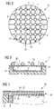
- FIG. 1 shows a carrier sheet 3 , on the upper side 4 of which semiconductor chips 1 have been applied in semiconductor device positions 2 that are arranged in rows and columns to produce a workpiece, which in this embodiment is a panel.
- workpiece is understood as meaning an article that is still intended for further processing, for example an intermediate product in the production of semiconductor devices, such as a panel.
- the semiconductor chips 1 have previously been singulated from a semiconductor wafer. Interspaces 16 are formed between the semiconductor chips 1 .
- the semiconductor chips 1 have first main surfaces 5 with active semiconductor chip structures such as integrated circuits and contact areas 6 .
- the side faces 7 and the second main surfaces 8 of the semiconductor chips 1 are passive.
- active regions may also be arranged on the second main surface of the semiconductor chips or on the first and second main surfaces.
- a further method step is represented in FIG. 2 .
- An electrically conducting layer 9 is applied to regions of the second main surfaces 8 and the side faces 7 of the semiconductor chips 1 .
- the electrically conducting layer 9 thereby also covers regions of the upper side 4 of the carrier 3 in the interspaces 16 between the semiconductor chips and in this way connects the semiconductor chips 1 to one another in an electrically conducting manner.
- the electrically conducting layer 9 is not applied directly to the side faces 7 , but instead an intermediate layer is arranged between the side faces 7 and the electrically conducting layer 9 and may be formed for example like a ramp. Such a ramp can facilitate uniform application of the electrically conducting layer 9 .
- the electrically conducting layer 9 typically has a thickness d of less than 100 ⁇ m, if it is produced from a filled or electrically conducting polymer. Layer thicknesses of 20 ⁇ m ⁇ d ⁇ 50 ⁇ m are advantageous for example. If the electrically conducting layer 9 is produced from a metal, it typically has a layer thickness d of a few micrometers or tenths of a micrometer, for example 0.1 ⁇ m ⁇ d ⁇ 2 ⁇ m.
- the electrically conducting layer 9 has interfaces with the carrier 3 . In a later stage of the method, when the carrier 3 is removed, these interfaces become exposed contact regions 15 , by means of which the electrically conducting layer 9 is accessible for electrical contacting.
- the semiconductor chips 1 are embedded with their side faces 7 and their second main surfaces 8 in a molding compound 10 .
- the workpiece 12 is obtained as a composite sheet comprising semiconductor chips 1 , molding compound 10 and electrically conducting layer 9 .
- the carrier sheet 3 is covered by the electrically conducting layer 9 in the entire region of the interspaces 16 .
- a closed layer is understood here as meaning a layer that is applied over a large surface area and covers the main part of the first main surface 11 of the workpiece 12 outside chip regions that are defined by the first main surfaces of the semiconductor chips.
- the first main surfaces 5 of the semiconductor chips 1 and regions of the electrically conducting layer 9 on the first main surface 11 of the workpiece 12 are exposed, but no molding compound 10 is exposed.
- the electrically conducting layer 9 is formed as a grid structure and only covers regions of the second main surfaces 8 and possibly of the side faces 7 and the interspaces 16 .
- the grid structure in this case comprises for example rows and columns of the electrically conducting layer 9 , the grid being so closely meshed that there is at least one column respectively crossing a row on the second main surface 8 of a semiconductor chip 1 .
- the molding compound 10 penetrates inbetween, to the upper side 4 of the carrier sheet 3 , and after removal of the carrier sheet 3 is exposed on the front side 11 of the workpiece 12 .
- the front side 11 of the workpiece 12 is consequently a coplanar surface comprising the first main surfaces 5 of the semiconductor chips 1 in the semiconductor device positions 2 , contact regions 15 of the electrically conducting layer 9 and possibly molding compound 10 .
- the electrically conducting layer 9 is formed for example from a conductive polymer, a metal or a plastic with electrically conducting particles. Application is performed, for example, by printing on a conductive polymer or a conductive ink, by vapor deposition, by sputtering or by placing on a metal mesh or a netting or a gauze-like fabric of a conductive polymer.
- thermoplastic or thermosetting material is provided as the molding compound 10 , and is applied for example by injection-molding onto the electrically conducting layer 9 .
- FIG. 4 schematically shows a cross section through the workpiece 12 produced, after removal of the carrier sheet 3 .
- the first main surfaces 5 of the semiconductor chips 1 which in this embodiment have active structures, are exposed on the first main surface 11 of the workpiece 12 .
- the first main surface 11 of the workpiece 12 is a coplanar surface comprising the first main surfaces 5 of the semiconductor chips 1 , contact regions 15 of the electrically conducting layer 9 and possibly molding compound 10 .
- the electrically conducting layer 9 is exposed on the first main surface 11 of the workpiece 12 and can be contacted for discharging the workpiece 12 or for preventing electrostatic charging.
- the second main surface 34 of the workpiece 12 is formed by the molding compound 10 .
- FIG. 5 shows a plan view of the first main surface 11 of the workpiece 12 after removal of the carrier sheet 3 .
- the workpiece is formed as a panel with semiconductor chips 1 arranged in rows and columns, which has the form and the dimensions of a semiconductor wafer.
- the electrically conducting layer 9 has been applied in continuous strips 25 , which follow in their direction the rows 14 and columns 13 in which the semiconductor chips 1 are arranged in the semiconductor device positions 2 .
- two strips 25 from directions perpendicular to each other respectively cross on the second main surface 8 of a semiconductor chip 1 , with the result that the electrically conducting layer 9 forms a grid, semiconductor chips 1 respectively being arranged on the grid points. In this way, all the semiconductor chips 1 of a panel can be conductively connected to one another in a simple way.
- the conductive strips 25 which respectively form the rows 14 and columns 13 , are exposed in the interspaces 16 between the semiconductor chips 1 on the first main surface 11 of the workpiece 12 , where they form contact regions 15 . Since, however, only these conductive strips 25 are exposed, and the remaining surface area of the first main surface 11 of the workpiece 12 that is not taken up by the first main surfaces 5 of the semiconductor chips 1 is formed by molding compound 10 , adequate electrically insulating surface area is available for the arrangement of other elements, for example external contact areas for semiconductor devices.
- the first main surface 11 of the workpiece 12 is a coplanar surface comprising the first main surfaces 5 of the semiconductor chips 1 , regions of the molding compound 10 and contact regions 15 of the electrically conducting layer 9 , it being possible for all the semiconductor chips 1 to be electrically contacted by means of the contact regions 15 .
- a wiring structure with interconnects and external contacts can be applied to the then exposed first main surface 11 of the workpiece 12 .
- the electrically conducting layer 9 is formed as a grid structure.
- the grid is more closely meshed, with the result that a number of rows 14 and columns 13 respectively cross on the second main surface 8 of a semiconductor chip 1 .
- the electrically conducting layer 9 may also be differently formed, for example as a substantially closed layer.
- a closed layer has the advantage that it can be applied particularly simply. However, in this case the entire, or virtually entire, region of the first main surface 11 of the workpiece 12 that is not taken up by the first main surfaces 5 of the semiconductor chips 1 is covered by the conductive layer 9 . In order to form wiring structures and/or external contacts on it, an insulating layer must first be applied again, it being possible for contact regions 15 to be left exposed.
- the contact regions 15 permit the electrical contacting of all, or at least many, of the semiconductor chips 1 , which are connected to one another in an electrically conducting manner to form a contact group.
- This allows electrostatic charges of the workpiece 12 , for example a panel, to be prevented or dissipated as quickly as possible during processing.
- it is not necessary to handle and process devices that are susceptible to ESD only in a specially protected environment, for which relatively complex devices are required, such as ionizers for generating ionized ambient air and electrically conductive work surfaces that prevent electrostatic charging of the devices as completely as possible.
- low charges of the workpiece 12 during processing are specifically dissipated before they reach a critical value, by contacting of the electrically conducting layer 9 in the contact regions 15 .
- the semiconductor chips 1 in the workpiece 12 are conductively connected to one another by a discharge structure in the form of the electrically conducting layer 9 , and contact regions 15 on the first main surface 11 of the workpiece 12 are created to allow easy access to the entire discharge structure, with the result that a potential equalization can take place at any time during processing to dissipate possible charges.
- the electrically conducting layer 9 is contiguous, single contacting is sufficient to discharge the entire workpiece 12 . If, on the other hand, the workpiece 12 is to be discharged region by region, for example row by row or column by column, the electrically conducting layer may also be made up of a number of partial regions that are insulated from one another.
- the resistance of the electrically conducting layer 9 may also be greater than that of a metallic layer. Therefore, not only metals are conceivable as materials for the layer 9 , but also for example electrically conducting polymers or plastics with electrically conducting particles. This has the advantage that the material for the layer 9 can be selected on the basis of other criteria, for example on the basis of easy applicability and processability.
- FIG. 6 schematically shows a cross section through a semiconductor device 17 , which has been singulated from the workpiece 12 according to FIGS. 4 and 5 , for example by sawing along dicing tracks that are not shown.
- the semiconductor device 17 has a semiconductor chip 1 , which is embedded with its side faces 7 and its second main surface 8 in a molding compound 10 .
- An electrically conducting layer 9 is arranged along the semiconductor chip contour on the side faces 7 and the first main surface 8 .
- only regions of the first main surface 26 of the semiconductor device 17 are formed by contact regions of the electrically conducting layer 9 , these contact regions not being visible in the sectional view that is shown.
- the second main surface 37 of the semiconductor device 17 is formed by the molding compound 10 .
- the semiconductor device has on its first main surface 26 a wiring layer 18 , which is typically multilayered, and external contacts 19 .
- the cutout 20 is represented in detail in FIG. 7 .
- FIG. 7 shows the cutout 20 from FIG. 6 .
- the wiring layer 18 in this case comprises three layers, to be specific one layer of a dielectric 22 directly on the first main surface 5 of the semiconductor chip 1 or on the first main surface 26 of the semiconductor device 17 , an electrically conductive layer on that, which forms interconnects 23 , and a further insulating layer of a dielectric 24 .
- the electrically conducting layer 9 In the contact region 15 , the electrically conducting layer 9 butts against the first main surface 26 of the semiconductor device 17 . At this point, the interconnect 23 is in electrical contact with the electrically conducting layer 9 . In this way, the electrically conducting layer can be contacted by means of the external contacts of the semiconductor device 17 also in the case of the finished semiconductor device 17 , in which the contact regions 15 themselves are no longer exposed.
- the molding compound 10 covering the electrically conducting layer 9 forms a plastic package for the semiconductor device 17 .
- FIG. 8 schematically shows a step of a method for producing a workpiece according to a second embodiment of the disclosure. It is also the case with this embodiment that, in a first method step, a number of semiconductor chips 1 are applied with their first main surfaces 5 onto the upper side 4 of a carrier sheet 3 , interspaces 16 being arranged between the semiconductor chips 1 .
- FIG. 9 shows a further step of the method according to the second embodiment.
- An insulating layer 27 of an electrically insulating material is first arranged on the second main surfaces 8 of the semiconductor chips 1 , and possibly also on the side faces 7 . Parylene or polyimide is used for example as the insulating material.
- the insulating layer 27 may, for example, be vapor-deposited or applied by placing on an electrically insulating film.
- the depositing of a parylene layer as an insulating layer 27 is performed for example by gas-phase polymerization: firstly, the dimer of the compound is vaporized.
- the dimer is prepared for example by dehydrating pyrolitic dimerization of p-xylene and subsequent quenching in liquid p-xylene. In this way, [2,2]-p-cyclophane is obtained.
- the dimer splits into two bivalent radical monomers such as p-xylene.
- the polymerization takes place on cooling. By this process, a very pure parylene coating can be deposited.
- the vaporization is carried out for example at a temperature of 160° C. to 180° C. and a pressure of 1-2 mbar and the pyrolysis is carried out at a temperature of 660° C. to 690° C. and a pressure of 0.5-1 mbar.
- the polymerization takes place for example at a temperature of less than 35° C. and a pressure of 0.1-0.2 mbar. This process permits very uniform deposition of the insulating layer 27 , which as a result has virtually the same thickness in all regions.
- the electrically conducting layer 9 is applied to the insulating layer 27 , with the result that the insulating layer 27 is arranged between the semiconductor chips 1 and the electrically conducting layer 9 .
- the electrically conducting layer 9 may be formed from a conductive polymer, a metal or a plastic with electrically conducting particles. Application is likewise performed, for example, by printing on a conductive polymer or a conductive ink, by vapor deposition, by sputtering or by placing on a metal mesh or a netting or a gauze-like fabric of a conductive polymer.
- the electrically conducting layer 9 forms an electromagnetic shielding of the semiconductor chips 1 .
- Such a shielding protects the semiconductor chips 1 from disturbing influences of electromagnetic radiation, which is necessary in particular in the case of applications such as baseband processors, power management units or radio-frequency circuits.
- a molding compound 10 is arranged on the electrically conducting layer 9 , with the result that the second main surface 34 of the workpiece 12 is formed by the molding compound 10 .
- a thermoplastic or thermosetting material which is applied to the electrically conducting layer 9 by injection molding, for example, is provided as the molding compound 10 .
- the side faces 7 and the second main surfaces 8 of the semiconductor chips 1 are embedded in the molding compound 10 .
- the workpiece 12 is formed as a panel with semiconductor chips 1 arranged in rows and columns at semiconductor device positions 2 .
- the method described according to the second embodiment makes it possible to apply the electromagnetic shielding to all the semiconductor chips 1 of a panel already at the wafer level.
- the shielding is accordingly firmly integrated in the package of the semiconductor devices, with the result that a particularly compact semiconductor device and at the same time a particularly simple production method can be provided.
- the carrier sheet 3 is removed, with the result that the first main surfaces 5 of the semiconductor chips 1 and regions 28 of the insulating layer 27 , which together form a coplanar surface and the first main surface 11 of the workpiece 12 , are exposed. Then, as described above, a wiring layer is applied to the exposed first main surface 11 .
- FIG. 12 schematically shows a further method step according to the second embodiment.
- the carrier sheet has already been removed from the first main surface 11 of the workpiece 12 and a dielectric layer 31 has been applied as part of a wiring layer to the first main surface 11 .
- a dielectric layer 31 In the dielectric layer 31 , vias 29 or through-holes for shielding and vias 30 to contact areas 6 of the semiconductor chips 1 are opened, for example by a (dry or wet) etching process or by laser ablation.
- FIG. 13 shows a further method step, in which a metallization 32 is applied as part of a wiring layer.
- the electrically conducting layer 9 is contacted through the vias 29 and the contact areas 6 of the semiconductor chips 11 are contacted through the vias 30 .
- external contact areas 35 for applying external contacts are formed.
- FIG. 14 shows a subsequent method step, in which a solder resist layer 33 has been applied to the dielectric layer 31 and structured, in order to leave the external contact areas 35 exposed for applying external contacts.
- External contacts 19 are applied to the external contact areas 35 , for example in the form of solder balls.
- the workpiece 12 can subsequently be divided up along dicing tracks, which are indicated by the dashed lines 36 , into individual semiconductor devices, for example by sawing.
- FIG. 15 A completed semiconductor device 17 according to the second embodiment of the disclosure is shown in FIG. 15 .
- the semiconductor device 17 has a semiconductor chip 1 with the first main surface 5 , the second main surface 8 and the side faces 7 .
- the electrically conducting layer 9 arranged on the semiconductor chip 1 which layer is arranged at least on regions of the second main surface 8 , forms an electromagnetic shielding of the semiconductor chips 1 .
- the insulating layer 27 is arranged between the semiconductor chip 1 and the electrically conducting layer 9 .
- Arranged on the electrically conducting layer 9 is the molding compound 19 , which forms the plastic package of the semiconductor device 17 .
- regions 28 of the insulating layer 27 form a coplanar surface with the first main surface 5 of the semiconductor chip 1 on a first main surface 26 of the semiconductor device 17 .
- the first main surface 26 of the semiconductor device 17 has a wiring structure or wiring layer 18 , which comprises at least the dielectric layer 31 , the metallization 32 with the external contact areas 35 and the solder resist layer 33 .
- the wiring layer 18 may, however, also be of a multilayered form and have a number of metallization layers and further contact vias.
- the electrically conducting layer 9 can also be electrically contacted and connected to a predetermined potential. It is also the case in this embodiment that the second main surface 37 of the semiconductor device 17 is formed by the molding compound 10 .
Abstract
Description
Claims (15)
Priority Applications (2)
| Application Number | Priority Date | Filing Date | Title |
|---|---|---|---|
| US14/330,066 US9293423B2 (en) | 2007-04-30 | 2014-07-14 | Workpiece with semiconductor chips, semiconductor device and method for producing a workpiece with semiconductor chips |
| US15/041,127 US9601475B2 (en) | 2007-04-30 | 2016-02-11 | Workpiece with semiconductor chips, semiconductor device and method for producing a workpiece with semiconductor chips |
Applications Claiming Priority (6)
| Application Number | Priority Date | Filing Date | Title |
|---|---|---|---|
| DE102007020656.0 | 2007-04-30 | ||
| DE102007020656A DE102007020656B4 (en) | 2007-04-30 | 2007-04-30 | Semiconductor chip workpiece, semiconductor device, and method of manufacturing a semiconductor chip workpiece |
| DE102007020656 | 2007-04-30 | ||
| US11/746,936 US8309454B2 (en) | 2007-04-30 | 2007-05-10 | Structure for electrostatic discharge in embedded wafer level packages |
| US13/673,318 US8779563B2 (en) | 2007-04-30 | 2012-11-09 | Workpiece with semiconductor chips, semiconductor device and method for producing a workpiece with semiconductor chips |
| US14/330,066 US9293423B2 (en) | 2007-04-30 | 2014-07-14 | Workpiece with semiconductor chips, semiconductor device and method for producing a workpiece with semiconductor chips |
Related Parent Applications (1)
| Application Number | Title | Priority Date | Filing Date |
|---|---|---|---|
| US13/673,318 Continuation US8779563B2 (en) | 2007-04-30 | 2012-11-09 | Workpiece with semiconductor chips, semiconductor device and method for producing a workpiece with semiconductor chips |
Related Child Applications (1)
| Application Number | Title | Priority Date | Filing Date |
|---|---|---|---|
| US15/041,127 Division US9601475B2 (en) | 2007-04-30 | 2016-02-11 | Workpiece with semiconductor chips, semiconductor device and method for producing a workpiece with semiconductor chips |
Publications (2)
| Publication Number | Publication Date |
|---|---|
| US20140332937A1 US20140332937A1 (en) | 2014-11-13 |
| US9293423B2 true US9293423B2 (en) | 2016-03-22 |
Family
ID=39809567
Family Applications (4)
| Application Number | Title | Priority Date | Filing Date |
|---|---|---|---|
| US11/746,936 Active 2028-09-16 US8309454B2 (en) | 2007-04-30 | 2007-05-10 | Structure for electrostatic discharge in embedded wafer level packages |
| US13/673,318 Active US8779563B2 (en) | 2007-04-30 | 2012-11-09 | Workpiece with semiconductor chips, semiconductor device and method for producing a workpiece with semiconductor chips |
| US14/330,066 Active US9293423B2 (en) | 2007-04-30 | 2014-07-14 | Workpiece with semiconductor chips, semiconductor device and method for producing a workpiece with semiconductor chips |
| US15/041,127 Active US9601475B2 (en) | 2007-04-30 | 2016-02-11 | Workpiece with semiconductor chips, semiconductor device and method for producing a workpiece with semiconductor chips |
Family Applications Before (2)
| Application Number | Title | Priority Date | Filing Date |
|---|---|---|---|
| US11/746,936 Active 2028-09-16 US8309454B2 (en) | 2007-04-30 | 2007-05-10 | Structure for electrostatic discharge in embedded wafer level packages |
| US13/673,318 Active US8779563B2 (en) | 2007-04-30 | 2012-11-09 | Workpiece with semiconductor chips, semiconductor device and method for producing a workpiece with semiconductor chips |
Family Applications After (1)
| Application Number | Title | Priority Date | Filing Date |
|---|---|---|---|
| US15/041,127 Active US9601475B2 (en) | 2007-04-30 | 2016-02-11 | Workpiece with semiconductor chips, semiconductor device and method for producing a workpiece with semiconductor chips |
Country Status (2)
| Country | Link |
|---|---|
| US (4) | US8309454B2 (en) |
| DE (1) | DE102007020656B4 (en) |
Cited By (5)
| Publication number | Priority date | Publication date | Assignee | Title |
|---|---|---|---|---|
| US20160254236A1 (en) * | 2015-02-27 | 2016-09-01 | Qualcomm Incorporated | Compartment shielding in flip-chip (fc) module |
| WO2018206594A1 (en) | 2017-05-12 | 2018-11-15 | Magna Powertrain Bad Homburg GmbH | Component having emv protection for an electronic board |
| US20180374718A1 (en) * | 2017-06-23 | 2018-12-27 | Applied Materials, Inc. | Method of reconstituted substrate formation for advanced packaging applications |
| US20200287518A1 (en) * | 2017-09-29 | 2020-09-10 | Nagase Chemtex Corporation | Manufacturing method of mounting structure, and laminate sheet therefor |
| US10861822B2 (en) * | 2018-09-04 | 2020-12-08 | Ningbo Semiconductor International Corporation | Wafer-level packaging method and package structure thereof |
Families Citing this family (84)
| Publication number | Priority date | Publication date | Assignee | Title |
|---|---|---|---|---|
| DE102007020656B4 (en) | 2007-04-30 | 2009-05-07 | Infineon Technologies Ag | Semiconductor chip workpiece, semiconductor device, and method of manufacturing a semiconductor chip workpiece |
| US7648858B2 (en) * | 2007-06-19 | 2010-01-19 | Freescale Semiconductor, Inc. | Methods and apparatus for EMI shielding in multi-chip modules |
| US8093689B2 (en) | 2007-07-02 | 2012-01-10 | Infineon Technologies Ag | Attachment member for semiconductor sensor device |
| US20090091005A1 (en) * | 2007-10-09 | 2009-04-09 | Huang Chung-Er | Shielding structure for semiconductors and manufacturing method therefor |
| US20090184414A1 (en) * | 2008-01-22 | 2009-07-23 | Chang Jun Park | Wafer level chip scale package having an enhanced heat exchange efficiency with an emf shield and a method for fabricating the same |
| US8008753B1 (en) * | 2008-04-22 | 2011-08-30 | Amkor Technology, Inc. | System and method to reduce shorting of radio frequency (RF) shielding |
| US9123663B2 (en) * | 2008-06-10 | 2015-09-01 | Stats Chippac, Ltd. | Semiconductor device and method of forming shielding layer grounded through metal pillars formed in peripheral region of the semiconductor |
| US7981730B2 (en) * | 2008-07-09 | 2011-07-19 | Freescale Semiconductor, Inc. | Integrated conformal shielding method and process using redistributed chip packaging |
| CN105161427B (en) * | 2008-11-17 | 2019-12-06 | 先进封装技术私人有限公司 | Semiconductor substrate, semiconductor package and method for manufacturing semiconductor device |
| US8119454B2 (en) * | 2008-12-08 | 2012-02-21 | Stmicroelectronics Asia Pacific Pte Ltd. | Manufacturing fan-out wafer level packaging |
| DE102009002376A1 (en) | 2009-04-15 | 2010-10-21 | Robert Bosch Gmbh | Multichip sensor module and method of making same |
| TWI497679B (en) * | 2009-11-27 | 2015-08-21 | Advanced Semiconductor Eng | Semiconductor package and manufacturing method thereof |
| US8569894B2 (en) | 2010-01-13 | 2013-10-29 | Advanced Semiconductor Engineering, Inc. | Semiconductor package with single sided substrate design and manufacturing methods thereof |
| US8409926B2 (en) * | 2010-03-09 | 2013-04-02 | Stats Chippac, Ltd. | Semiconductor device and method of forming insulating layer around semiconductor die |
| TWI411075B (en) | 2010-03-22 | 2013-10-01 | Advanced Semiconductor Eng | Semiconductor package and manufacturing method thereof |
| US8319318B2 (en) * | 2010-04-06 | 2012-11-27 | Intel Corporation | Forming metal filled die back-side film for electromagnetic interference shielding with coreless packages |
| US8258012B2 (en) * | 2010-05-14 | 2012-09-04 | Stats Chippac, Ltd. | Semiconductor device and method of forming discontinuous ESD protection layers between semiconductor die |
| DE102010029550B4 (en) | 2010-06-01 | 2019-08-22 | Robert Bosch Gmbh | Process for the production of semiconductor devices |
| CN102339763B (en) * | 2010-07-21 | 2016-01-27 | 飞思卡尔半导体公司 | The method of assembling integrated circuit (IC)-components |
| JP5636497B2 (en) | 2010-08-05 | 2014-12-03 | エプコス アーゲーEpcos Ag | Method for manufacturing electronic device assembly having electromagnetic shield and heat radiation portion, and electronic device having electromagnetic shield and heat radiation portion |
| DE102010033551A1 (en) * | 2010-08-05 | 2012-02-09 | Epcos Ag | Method for producing a plurality of electromagnetic shielded electronic components and electromagnetic shielded electronic component |
| CN102446870A (en) * | 2010-10-13 | 2012-05-09 | 矽品精密工业股份有限公司 | Packaging component with electrostatic discharge and anti-interference of electromagnetic wave functions |
| US9064879B2 (en) * | 2010-10-14 | 2015-06-23 | Taiwan Semiconductor Manufacturing Company, Ltd. | Packaging methods and structures using a die attach film |
| US8936966B2 (en) | 2012-02-08 | 2015-01-20 | Taiwan Semiconductor Manufacturing Company, Ltd. | Packaging methods for semiconductor devices |
| US8105875B1 (en) | 2010-10-14 | 2012-01-31 | Taiwan Semiconductor Manufacturing Company, Ltd. | Approach for bonding dies onto interposers |
| US8941222B2 (en) | 2010-11-11 | 2015-01-27 | Advanced Semiconductor Engineering Inc. | Wafer level semiconductor package and manufacturing methods thereof |
| US9406658B2 (en) | 2010-12-17 | 2016-08-02 | Advanced Semiconductor Engineering, Inc. | Embedded component device and manufacturing methods thereof |
| US8569861B2 (en) | 2010-12-22 | 2013-10-29 | Analog Devices, Inc. | Vertically integrated systems |
| FR2974942B1 (en) | 2011-05-06 | 2016-07-29 | 3D Plus | PROCESS FOR PRODUCING RECONSTITUTED PLATES WITH THE MAINTENANCE OF CHIPS DURING THEIR ENCAPSULATION |
| US9196588B2 (en) * | 2011-11-04 | 2015-11-24 | Invensas Corporation | EMI shield |
| WO2014132937A1 (en) | 2013-02-28 | 2014-09-04 | 株式会社村田製作所 | Esd protection device |
| GB2525774A (en) | 2013-02-28 | 2015-11-04 | Murata Manufacturing Co | Semiconductor device |
| CN205508776U (en) | 2013-02-28 | 2016-08-24 | 株式会社村田制作所 | Semiconductor device |
| CN205104477U (en) * | 2013-04-05 | 2016-03-23 | 株式会社村田制作所 | ESD protection device |
| US10015916B1 (en) * | 2013-05-21 | 2018-07-03 | Xilinx, Inc. | Removal of electrostatic charges from an interposer via a ground pad thereof for die attach for formation of a stacked die |
| US9960227B2 (en) | 2013-09-11 | 2018-05-01 | Xilinx, Inc. | Removal of electrostatic charges from interposer for die attachment |
| US9576930B2 (en) | 2013-11-08 | 2017-02-21 | Taiwan Semiconductor Manufacturing Co., Ltd. | Thermally conductive structure for heat dissipation in semiconductor packages |
| US10586771B2 (en) * | 2013-12-16 | 2020-03-10 | Utac Headquarters Pte, Ltd | Conductive shield for semiconductor package |
| TWI584387B (en) * | 2014-08-15 | 2017-05-21 | 矽品精密工業股份有限公司 | Method of manufacturing package structure |
| US11069734B2 (en) | 2014-12-11 | 2021-07-20 | Invensas Corporation | Image sensor device |
| US9461005B2 (en) * | 2015-02-12 | 2016-10-04 | Ampleon Netherlands B.V. | RF package with non-gaseous dielectric material |
| US10269686B1 (en) * | 2015-05-27 | 2019-04-23 | UTAC Headquarters PTE, LTD. | Method of improving adhesion between molding compounds and an apparatus thereof |
| US9741620B2 (en) | 2015-06-24 | 2017-08-22 | Invensas Corporation | Structures and methods for reliable packages |
| US10446532B2 (en) | 2016-01-13 | 2019-10-15 | Invensas Bonding Technologies, Inc. | Systems and methods for efficient transfer of semiconductor elements |
| US11189573B2 (en) * | 2016-03-31 | 2021-11-30 | Intel Corporation | Semiconductor package with electromagnetic interference shielding using metal layers and vias |
| KR101858952B1 (en) * | 2016-05-13 | 2018-05-18 | 주식회사 네패스 | Semiconductor package and method of manufacturing the same |
| US10204893B2 (en) | 2016-05-19 | 2019-02-12 | Invensas Bonding Technologies, Inc. | Stacked dies and methods for forming bonded structures |
| US10080317B2 (en) * | 2016-06-29 | 2018-09-18 | Microsoft Technology Licensing, Llc | Polymeric electromagnetic shield for electronic components |
| US10418341B2 (en) * | 2016-08-31 | 2019-09-17 | STATS ChipPAC Pte. Ltd. | Semiconductor device and method of forming SIP with electrical component terminals extending out from encapsulant |
| US10879212B2 (en) | 2017-05-11 | 2020-12-29 | Invensas Bonding Technologies, Inc. | Processed stacked dies |
| US10217720B2 (en) | 2017-06-15 | 2019-02-26 | Invensas Corporation | Multi-chip modules formed using wafer-level processing of a reconstitute wafer |
| US10804115B2 (en) * | 2017-08-03 | 2020-10-13 | General Electric Company | Electronics package with integrated interconnect structure and method of manufacturing thereof |
| US10541209B2 (en) * | 2017-08-03 | 2020-01-21 | General Electric Company | Electronics package including integrated electromagnetic interference shield and method of manufacturing thereof |
| US10541153B2 (en) | 2017-08-03 | 2020-01-21 | General Electric Company | Electronics package with integrated interconnect structure and method of manufacturing thereof |
| US20190043794A1 (en) * | 2017-08-03 | 2019-02-07 | General Electric Company | Electronics package including integrated structure with backside functionality and method of manufacturing thereof |
| CN110998830B (en) * | 2017-08-21 | 2023-09-22 | 株式会社村田制作所 | Electronic component module and method for manufacturing electronic component module |
| US10730743B2 (en) | 2017-11-06 | 2020-08-04 | Analog Devices Global Unlimited Company | Gas sensor packages |
| KR20190075647A (en) * | 2017-12-21 | 2019-07-01 | 삼성전자주식회사 | Fan-out semiconductor package |
| KR102196173B1 (en) * | 2018-01-29 | 2020-12-30 | 주식회사 네패스 | Semiconductor package and method of manufacturing the same |
| US11276676B2 (en) | 2018-05-15 | 2022-03-15 | Invensas Bonding Technologies, Inc. | Stacked devices and methods of fabrication |
| CN108601241B (en) * | 2018-06-14 | 2021-12-24 | 环旭电子股份有限公司 | SiP module and manufacturing method thereof |
| WO2020010136A1 (en) | 2018-07-06 | 2020-01-09 | Invensas Bonding Technologies, Inc. | Molded direct bonded and interconnected stack |
| US11462419B2 (en) | 2018-07-06 | 2022-10-04 | Invensas Bonding Technologies, Inc. | Microelectronic assemblies |
| CN110875199B (en) * | 2018-09-04 | 2021-12-10 | 中芯集成电路(宁波)有限公司 | Wafer level packaging method and packaging structure |
| CN110875204B (en) * | 2018-09-04 | 2022-03-18 | 中芯集成电路(宁波)有限公司 | Wafer level packaging method and packaging structure |
| US10978421B2 (en) * | 2018-09-04 | 2021-04-13 | Ningbo Semiconductor International Corporation | Wafer-level packaging method and package structure |
| WO2020150159A1 (en) | 2019-01-14 | 2020-07-23 | Invensas Bonding Technologies, Inc. | Bonded structures |
| WO2020250823A1 (en) * | 2019-06-13 | 2020-12-17 | 株式会社村田製作所 | Module |
| US11587839B2 (en) | 2019-06-27 | 2023-02-21 | Analog Devices, Inc. | Device with chemical reaction chamber |
| WO2021006141A1 (en) * | 2019-07-08 | 2021-01-14 | 株式会社村田製作所 | Module and method for manufacturing same |
| CN110718535B (en) * | 2019-07-26 | 2021-07-02 | 南通通富微电子有限公司 | Packaging structure |
| CN110534502B (en) * | 2019-07-26 | 2021-12-10 | 南通通富微电子有限公司 | Packaging structure |
| CN110473844B (en) * | 2019-07-26 | 2021-07-02 | 通富微电子股份有限公司 | Packaging structure |
| CN110718473B (en) * | 2019-07-26 | 2021-08-27 | 南通通富微电子有限公司 | Forming method of packaging structure |
| CN110518002B (en) * | 2019-07-26 | 2023-04-07 | 通富微电子股份有限公司 | Forming method of packaging structure |
| CN110473859B (en) * | 2019-07-26 | 2021-07-02 | 南通通富微电子有限公司 | Packaging structure |
| CN110544677B (en) * | 2019-07-26 | 2023-03-14 | 通富微电子股份有限公司 | Packaging structure |
| CN110718536B (en) * | 2019-07-26 | 2021-08-27 | 南通通富微电子有限公司 | Packaging structure |
| WO2021017898A1 (en) * | 2019-07-26 | 2021-02-04 | Nantong Tongfu Microelectronics Co., Ltd | Packaging structure andformation method thereof |
| CN110534442B (en) * | 2019-07-26 | 2023-03-14 | 通富微电子股份有限公司 | Forming method of packaging structure |
| WO2021017896A1 (en) * | 2019-07-26 | 2021-02-04 | Tongfu Microelectronics Co., Ltd. | Packaging structure and fabrication method thereof |
| US11631647B2 (en) | 2020-06-30 | 2023-04-18 | Adeia Semiconductor Bonding Technologies Inc. | Integrated device packages with integrated device die and dummy element |
| US11728273B2 (en) | 2020-09-04 | 2023-08-15 | Adeia Semiconductor Bonding Technologies Inc. | Bonded structure with interconnect structure |
| US11764177B2 (en) | 2020-09-04 | 2023-09-19 | Adeia Semiconductor Bonding Technologies Inc. | Bonded structure with interconnect structure |
Citations (46)
| Publication number | Priority date | Publication date | Assignee | Title |
|---|---|---|---|---|
| US5151769A (en) * | 1991-04-04 | 1992-09-29 | General Electric Company | Optically patterned RF shield for an integrated circuit chip for analog and/or digital operation at microwave frequencies |
| EP0611129A2 (en) | 1993-02-08 | 1994-08-17 | General Electric Company | Embedded substrate for integrated circuit modules |
| US5371404A (en) * | 1993-02-04 | 1994-12-06 | Motorola, Inc. | Thermally conductive integrated circuit package with radio frequency shielding |
| US5639989A (en) * | 1994-04-19 | 1997-06-17 | Motorola Inc. | Shielded electronic component assembly and method for making the same |
| US5814894A (en) | 1995-04-07 | 1998-09-29 | Nitto Denko Corporation | Semiconductor device, production method thereof, and tape carrier for semiconductor device used for producing the semiconductor device |
| US5866953A (en) | 1996-05-24 | 1999-02-02 | Micron Technology, Inc. | Packaged die on PCB with heat sink encapsulant |
| US6075289A (en) | 1996-10-24 | 2000-06-13 | Tessera, Inc. | Thermally enhanced packaged semiconductor assemblies |
| US6133634A (en) | 1998-08-05 | 2000-10-17 | Fairchild Semiconductor Corporation | High performance flip chip package |
| US6294731B1 (en) * | 1999-03-16 | 2001-09-25 | Performance Interconnect, Inc. | Apparatus for multichip packaging |
| US6444498B1 (en) | 2001-08-08 | 2002-09-03 | Siliconware Precision Industries Co., Ltd | Method of making semiconductor package with heat spreader |
| US6465893B1 (en) | 1990-09-24 | 2002-10-15 | Tessera, Inc. | Stacked chip assembly |
| US6472724B1 (en) * | 1999-04-19 | 2002-10-29 | Nec Corporation | Electronic device structure capable of preventing malfunction caused by electromagnetic wave coming from outside |
| US20020166686A1 (en) * | 2000-12-27 | 2002-11-14 | Junichi Toyoda | Sheet for electronic parts and method of producing the same |
| US6492194B1 (en) | 1999-10-15 | 2002-12-10 | Thomson-Csf | Method for the packaging of electronic components |
| US20030109077A1 (en) | 2001-12-07 | 2003-06-12 | Samsung Electro-Mechanics Co., Ltd. | Method for fabricating surface acoustic wave filter packages |
| US6602740B1 (en) | 1999-11-24 | 2003-08-05 | Tessera, Inc. | Encapsulation of microelectronic assemblies |
| FR2843485A1 (en) | 2002-08-06 | 2004-02-13 | Thales Sa | Fabrication of a module of integrated circuits with a substrate and a number of components using a support for the components and forming the substrate above them with the incorporation of a metal layer |
| US6722030B1 (en) | 1998-02-18 | 2004-04-20 | Epcos Ag | Process for manufacturing an electronic component, in particular a surface-wave component working with acoustic surface waves |
| US6838748B2 (en) | 2002-05-22 | 2005-01-04 | Sharp Kabushiki Kaisha | Semiconductor element with electromagnetic shielding layer on back/side face(s) thereof |
| US20050029666A1 (en) * | 2001-08-31 | 2005-02-10 | Yasutoshi Kurihara | Semiconductor device structural body and electronic device |
| US20050046001A1 (en) * | 2001-08-28 | 2005-03-03 | Tessera, Inc | High-frequency chip packages |
| US6929849B2 (en) | 2001-08-28 | 2005-08-16 | 3M Innovative Properties Company | Embedded electrical traces |
| US20050194666A1 (en) | 2003-01-21 | 2005-09-08 | Huang Chien P. | Semiconductor package free of substrate and fabrication method thereof |
| US6946740B2 (en) | 2002-07-15 | 2005-09-20 | International Rectifier Corporation | High power MCM package |
| US6962829B2 (en) | 1996-10-31 | 2005-11-08 | Amkor Technology, Inc. | Method of making near chip size integrated circuit package |
| US6992400B2 (en) | 2004-01-30 | 2006-01-31 | Nokia Corporation | Encapsulated electronics device with improved heat dissipation |
| US7045459B2 (en) | 2002-02-19 | 2006-05-16 | Northrop Grumman Corporation | Thin film encapsulation of MEMS devices |
| US20060145361A1 (en) | 2005-01-05 | 2006-07-06 | Yang Jun Y | Semiconductor device package and manufacturing method thereof |
| US7098074B2 (en) | 2002-11-13 | 2006-08-29 | Tessera, Inc. | Microelectronic assemblies having low profile connections |
| US20070045829A1 (en) | 2005-08-30 | 2007-03-01 | Samsung Electro-Mechanics Co., Ltd. | Backside ground type flip chip semiconductor package |
| US20070076390A1 (en) | 2005-09-30 | 2007-04-05 | Friedrich Kroener | Power semiconductor module |
| US20070123001A1 (en) | 2005-11-28 | 2007-05-31 | Xci Inc. A California Corporation | System and method for separating and packaging integrated circuits |
| US20070138614A1 (en) | 2005-12-16 | 2007-06-21 | Sige Semiconductor (U.S.), Corp. | Methods for integrated circuit module packaging and integrated circuit module packages |
| US20070145539A1 (en) | 2005-12-22 | 2007-06-28 | Ken Lam | Method and system for providing an integral radio frequency shield in a molded array package |
| US20070145541A1 (en) * | 2005-05-06 | 2007-06-28 | Samsung Electro-Mechanics Co., Ltd. | Stack type surface acoustic wave package, and method for manufacturing the same |
| US7259041B2 (en) | 2001-12-28 | 2007-08-21 | Epcos Ag | Method for the hermetic encapsulation of a component |
| US7282804B2 (en) | 2001-09-17 | 2007-10-16 | Megica Corporation | Structure of high performance combo chip and processing method |
| US20070262436A1 (en) | 2006-05-12 | 2007-11-15 | Micron Technology, Inc. | Microelectronic devices and methods for manufacturing microelectronic devices |
| US7381583B1 (en) | 2004-05-24 | 2008-06-03 | The United States Of America As Represented By The Secretary Of The Air Force | MEMS RF switch integrated process |
| US7478474B2 (en) | 2005-05-25 | 2009-01-20 | Alps Electric Co., Ltd. | Method of manufacturing shielded electronic circuit units |
| US7552532B2 (en) | 2001-07-27 | 2009-06-30 | Epcos Ag | Method for hermetically encapsulating a component |
| US7629674B1 (en) * | 2004-11-17 | 2009-12-08 | Amkor Technology, Inc. | Shielded package having shield fence |
| US7659604B2 (en) | 2004-03-30 | 2010-02-09 | Panasonic Corporation | Module component and method for manufacturing the same |
| US7687895B2 (en) | 2007-04-30 | 2010-03-30 | Infineon Technologies Ag | Workpiece with semiconductor chips and molding, semiconductor device and method for producing a workpiece with semiconductors chips |
| US7978070B2 (en) | 2004-04-08 | 2011-07-12 | W. L. Gore & Associates (Uk) Ltd. | Tamper respondent enclosure |
| US8309454B2 (en) | 2007-04-30 | 2012-11-13 | Intel Mobile Communications GmbH | Structure for electrostatic discharge in embedded wafer level packages |
Family Cites Families (4)
| Publication number | Priority date | Publication date | Assignee | Title |
|---|---|---|---|---|
| CA2443782A1 (en) * | 2001-05-07 | 2002-11-14 | Dusan Milojevic | Process for manufacturing electrically conductive components |
| US20030059976A1 (en) * | 2001-09-24 | 2003-03-27 | Nathan Richard J. | Integrated package and methods for making same |
| US6602739B1 (en) * | 2001-10-31 | 2003-08-05 | Lockheed Martin Corporation | Method for making multichip module substrates by encapsulating electrical conductors and filling gaps |
| US6794222B1 (en) * | 2002-09-23 | 2004-09-21 | Lockheed Martin Corporation | HDI module with integral conductive electromagnetic shield |
-
2007
- 2007-04-30 DE DE102007020656A patent/DE102007020656B4/en active Active
- 2007-05-10 US US11/746,936 patent/US8309454B2/en active Active
-
2012
- 2012-11-09 US US13/673,318 patent/US8779563B2/en active Active
-
2014
- 2014-07-14 US US14/330,066 patent/US9293423B2/en active Active
-
2016
- 2016-02-11 US US15/041,127 patent/US9601475B2/en active Active
Patent Citations (47)
| Publication number | Priority date | Publication date | Assignee | Title |
|---|---|---|---|---|
| US6465893B1 (en) | 1990-09-24 | 2002-10-15 | Tessera, Inc. | Stacked chip assembly |
| US5151769A (en) * | 1991-04-04 | 1992-09-29 | General Electric Company | Optically patterned RF shield for an integrated circuit chip for analog and/or digital operation at microwave frequencies |
| US5371404A (en) * | 1993-02-04 | 1994-12-06 | Motorola, Inc. | Thermally conductive integrated circuit package with radio frequency shielding |
| EP0611129A2 (en) | 1993-02-08 | 1994-08-17 | General Electric Company | Embedded substrate for integrated circuit modules |
| US5639989A (en) * | 1994-04-19 | 1997-06-17 | Motorola Inc. | Shielded electronic component assembly and method for making the same |
| US5814894A (en) | 1995-04-07 | 1998-09-29 | Nitto Denko Corporation | Semiconductor device, production method thereof, and tape carrier for semiconductor device used for producing the semiconductor device |
| US5866953A (en) | 1996-05-24 | 1999-02-02 | Micron Technology, Inc. | Packaged die on PCB with heat sink encapsulant |
| US6075289A (en) | 1996-10-24 | 2000-06-13 | Tessera, Inc. | Thermally enhanced packaged semiconductor assemblies |
| US6962829B2 (en) | 1996-10-31 | 2005-11-08 | Amkor Technology, Inc. | Method of making near chip size integrated circuit package |
| US6722030B1 (en) | 1998-02-18 | 2004-04-20 | Epcos Ag | Process for manufacturing an electronic component, in particular a surface-wave component working with acoustic surface waves |
| US6133634A (en) | 1998-08-05 | 2000-10-17 | Fairchild Semiconductor Corporation | High performance flip chip package |
| US6294731B1 (en) * | 1999-03-16 | 2001-09-25 | Performance Interconnect, Inc. | Apparatus for multichip packaging |
| US6472724B1 (en) * | 1999-04-19 | 2002-10-29 | Nec Corporation | Electronic device structure capable of preventing malfunction caused by electromagnetic wave coming from outside |
| US6492194B1 (en) | 1999-10-15 | 2002-12-10 | Thomson-Csf | Method for the packaging of electronic components |
| US6602740B1 (en) | 1999-11-24 | 2003-08-05 | Tessera, Inc. | Encapsulation of microelectronic assemblies |
| US20020166686A1 (en) * | 2000-12-27 | 2002-11-14 | Junichi Toyoda | Sheet for electronic parts and method of producing the same |
| US7552532B2 (en) | 2001-07-27 | 2009-06-30 | Epcos Ag | Method for hermetically encapsulating a component |
| US6444498B1 (en) | 2001-08-08 | 2002-09-03 | Siliconware Precision Industries Co., Ltd | Method of making semiconductor package with heat spreader |
| US6929849B2 (en) | 2001-08-28 | 2005-08-16 | 3M Innovative Properties Company | Embedded electrical traces |
| US20050046001A1 (en) * | 2001-08-28 | 2005-03-03 | Tessera, Inc | High-frequency chip packages |
| US20050029666A1 (en) * | 2001-08-31 | 2005-02-10 | Yasutoshi Kurihara | Semiconductor device structural body and electronic device |
| US7282804B2 (en) | 2001-09-17 | 2007-10-16 | Megica Corporation | Structure of high performance combo chip and processing method |
| US20030109077A1 (en) | 2001-12-07 | 2003-06-12 | Samsung Electro-Mechanics Co., Ltd. | Method for fabricating surface acoustic wave filter packages |
| US7259041B2 (en) | 2001-12-28 | 2007-08-21 | Epcos Ag | Method for the hermetic encapsulation of a component |
| US7045459B2 (en) | 2002-02-19 | 2006-05-16 | Northrop Grumman Corporation | Thin film encapsulation of MEMS devices |
| US6838748B2 (en) | 2002-05-22 | 2005-01-04 | Sharp Kabushiki Kaisha | Semiconductor element with electromagnetic shielding layer on back/side face(s) thereof |
| US6946740B2 (en) | 2002-07-15 | 2005-09-20 | International Rectifier Corporation | High power MCM package |
| FR2843485A1 (en) | 2002-08-06 | 2004-02-13 | Thales Sa | Fabrication of a module of integrated circuits with a substrate and a number of components using a support for the components and forming the substrate above them with the incorporation of a metal layer |
| US7098074B2 (en) | 2002-11-13 | 2006-08-29 | Tessera, Inc. | Microelectronic assemblies having low profile connections |
| US20050194666A1 (en) | 2003-01-21 | 2005-09-08 | Huang Chien P. | Semiconductor package free of substrate and fabrication method thereof |
| US6992400B2 (en) | 2004-01-30 | 2006-01-31 | Nokia Corporation | Encapsulated electronics device with improved heat dissipation |
| US7659604B2 (en) | 2004-03-30 | 2010-02-09 | Panasonic Corporation | Module component and method for manufacturing the same |
| US7978070B2 (en) | 2004-04-08 | 2011-07-12 | W. L. Gore & Associates (Uk) Ltd. | Tamper respondent enclosure |
| US7381583B1 (en) | 2004-05-24 | 2008-06-03 | The United States Of America As Represented By The Secretary Of The Air Force | MEMS RF switch integrated process |
| US7629674B1 (en) * | 2004-11-17 | 2009-12-08 | Amkor Technology, Inc. | Shielded package having shield fence |
| US20060145361A1 (en) | 2005-01-05 | 2006-07-06 | Yang Jun Y | Semiconductor device package and manufacturing method thereof |
| US20070145541A1 (en) * | 2005-05-06 | 2007-06-28 | Samsung Electro-Mechanics Co., Ltd. | Stack type surface acoustic wave package, and method for manufacturing the same |
| US7478474B2 (en) | 2005-05-25 | 2009-01-20 | Alps Electric Co., Ltd. | Method of manufacturing shielded electronic circuit units |
| US20070045829A1 (en) | 2005-08-30 | 2007-03-01 | Samsung Electro-Mechanics Co., Ltd. | Backside ground type flip chip semiconductor package |
| US20070076390A1 (en) | 2005-09-30 | 2007-04-05 | Friedrich Kroener | Power semiconductor module |
| US20070123001A1 (en) | 2005-11-28 | 2007-05-31 | Xci Inc. A California Corporation | System and method for separating and packaging integrated circuits |
| US20070138614A1 (en) | 2005-12-16 | 2007-06-21 | Sige Semiconductor (U.S.), Corp. | Methods for integrated circuit module packaging and integrated circuit module packages |
| US20070145539A1 (en) | 2005-12-22 | 2007-06-28 | Ken Lam | Method and system for providing an integral radio frequency shield in a molded array package |
| US20070262436A1 (en) | 2006-05-12 | 2007-11-15 | Micron Technology, Inc. | Microelectronic devices and methods for manufacturing microelectronic devices |
| US7687895B2 (en) | 2007-04-30 | 2010-03-30 | Infineon Technologies Ag | Workpiece with semiconductor chips and molding, semiconductor device and method for producing a workpiece with semiconductors chips |
| US8309454B2 (en) | 2007-04-30 | 2012-11-13 | Intel Mobile Communications GmbH | Structure for electrostatic discharge in embedded wafer level packages |
| US20130228904A1 (en) | 2007-04-30 | 2013-09-05 | Intel Mobile Communications GmbH | Workpiece with Semiconductor Chips, Semiconductor Device and Method for Producing a Workpiece with Semiconductor Chips |
Non-Patent Citations (9)
| Title |
|---|
| Final Office Action dated Jan. 8, 2010 for U.S. Appl. No. 11/746,936. |
| Non-Final Office Action dated Apr. 20, 2009 for U.S. Appl. No. 11/939,938. |
| Non-Final Office Action dated Jul. 22, 2011 for U.S. Appl. No. 11/746,936. |
| Non-Final Office Action dated Jul. 9, 2009 for U.S. Appl. No. 11/746,936. |
| Non-Final Office Action dated Nov. 4, 2011 for U.S. Appl. No. 11/746,936. |
| Non-Final Office Action dated Sep. 19, 2013 for U.S. Appl. No. 13/673,318. 13 Pages. |
| Notice of Allowance dated Jul. 18, 2012 for U.S. Appl. No. 11/746,936. |
| Notice of Allowance dated Mar. 12, 2014 for U.S. Appl. No. 13/673,318. 24 Pages. |
| Notice of Allowance dated Nov. 17, 2009 for U.S. Appl. No. 11/939,938. |
Cited By (11)
| Publication number | Priority date | Publication date | Assignee | Title |
|---|---|---|---|---|
| US20160254236A1 (en) * | 2015-02-27 | 2016-09-01 | Qualcomm Incorporated | Compartment shielding in flip-chip (fc) module |
| US10242957B2 (en) * | 2015-02-27 | 2019-03-26 | Qualcomm Incorporated | Compartment shielding in flip-chip (FC) module |
| WO2018206594A1 (en) | 2017-05-12 | 2018-11-15 | Magna Powertrain Bad Homburg GmbH | Component having emv protection for an electronic board |
| DE102017208075A1 (en) * | 2017-05-12 | 2018-11-15 | Magna Powertrain Bad Homburg GmbH | Component with EMC protection for electronic board |
| US20180374718A1 (en) * | 2017-06-23 | 2018-12-27 | Applied Materials, Inc. | Method of reconstituted substrate formation for advanced packaging applications |
| US10211072B2 (en) * | 2017-06-23 | 2019-02-19 | Applied Materials, Inc. | Method of reconstituted substrate formation for advanced packaging applications |
| US20190181019A1 (en) * | 2017-06-23 | 2019-06-13 | Applied Materials, Inc. | Method of reconstituted substrate formation for advanced packaging applications |
| US20200287518A1 (en) * | 2017-09-29 | 2020-09-10 | Nagase Chemtex Corporation | Manufacturing method of mounting structure, and laminate sheet therefor |
| US11799442B2 (en) * | 2017-09-29 | 2023-10-24 | Nagase Chemtex Corporation | Manufacturing method of mounting structure, and laminate sheet therefor |
| US10861822B2 (en) * | 2018-09-04 | 2020-12-08 | Ningbo Semiconductor International Corporation | Wafer-level packaging method and package structure thereof |
| US11562980B2 (en) | 2018-09-04 | 2023-01-24 | Ningbo Semiconductor International Corporation | Wafer-level package structure |
Also Published As
| Publication number | Publication date |
|---|---|
| DE102007020656A1 (en) | 2008-11-06 |
| US20080265421A1 (en) | 2008-10-30 |
| US20130228904A1 (en) | 2013-09-05 |
| US8779563B2 (en) | 2014-07-15 |
| US20140332937A1 (en) | 2014-11-13 |
| US8309454B2 (en) | 2012-11-13 |
| DE102007020656B4 (en) | 2009-05-07 |
| US20160163682A1 (en) | 2016-06-09 |
| US9601475B2 (en) | 2017-03-21 |
Similar Documents
| Publication | Publication Date | Title |
|---|---|---|
| US9601475B2 (en) | Workpiece with semiconductor chips, semiconductor device and method for producing a workpiece with semiconductor chips | |
| US7687895B2 (en) | Workpiece with semiconductor chips and molding, semiconductor device and method for producing a workpiece with semiconductors chips | |
| US8004068B2 (en) | Shielded multi-layer package structures | |
| US11901348B2 (en) | Semiconductor package and method of manufacturing the semiconductor package | |
| US20190295944A1 (en) | Semiconductor package of using insulating frame | |
| JP4511561B2 (en) | SEMICONDUCTOR ELEMENT HAVING LAMINATED SEMICONDUCTOR CHIP AND MANUFACTURING METHOD | |
| US9263362B2 (en) | Method of forming a ring-shaped metal structure | |
| EP1317773B1 (en) | Build-up layer structure on an encapsulated die package having a moisture barrier structure | |
| US20170330839A1 (en) | Semiconductor package and method of manufacturing the same | |
| EP1739747A2 (en) | Semiconductor chip and method of manufacturing the same | |
| US9917036B2 (en) | Chip package and a wafer level package | |
| US9406646B2 (en) | Electronic device and method for fabricating an electronic device | |
| US20170186698A1 (en) | Electronic package having electromagnetic interference shielding and associated method | |
| KR100910233B1 (en) | Stacked wafer level package | |
| US20170006707A1 (en) | Electronic device module and method of manufacturing the same | |
| US10008454B1 (en) | Wafer level package with EMI shielding | |
| US20160035677A1 (en) | Method for forming a package arrangement and package arrangement | |
| US20080203526A1 (en) | Semiconductor device equipped with thin-film circuit elements | |
| US20220285256A1 (en) | Wafer level packaging having redistribution layer formed utilizing laser direct structuring | |
| CN217426718U (en) | Semiconductor package | |
| US20170345805A1 (en) | Package including stacked die and passive component | |
| US7923294B2 (en) | Semiconductor package and method for manufacturing the same for decreasing number of processes | |
| TW202017443A (en) | Circuit carrier and manifacturing method thereof |
Legal Events
| Date | Code | Title | Description |
|---|---|---|---|
| STCF | Information on status: patent grant |
Free format text: PATENTED CASE |
|
| MAFP | Maintenance fee payment |
Free format text: PAYMENT OF MAINTENANCE FEE, 4TH YEAR, LARGE ENTITY (ORIGINAL EVENT CODE: M1551); ENTITY STATUS OF PATENT OWNER: LARGE ENTITY Year of fee payment: 4 |
|
| AS | Assignment |
Owner name: INTEL CORPORATION, CALIFORNIA Free format text: ASSIGNMENT OF ASSIGNORS INTEREST;ASSIGNOR:INTEL DEUTSCHLAND GMBH;REEL/FRAME:061356/0001 Effective date: 20220708 |
|
| AS | Assignment |
Owner name: TAHOE RESEARCH, LTD., IRELAND Free format text: ASSIGNMENT OF ASSIGNORS INTEREST;ASSIGNOR:INTEL CORPORATION;REEL/FRAME:061827/0686 Effective date: 20220718 |
|
| MAFP | Maintenance fee payment |
Free format text: PAYMENT OF MAINTENANCE FEE, 8TH YEAR, LARGE ENTITY (ORIGINAL EVENT CODE: M1552); ENTITY STATUS OF PATENT OWNER: LARGE ENTITY Year of fee payment: 8 |