US9311268B1 - Method and system for communication with peripheral devices - Google Patents
Method and system for communication with peripheral devices Download PDFInfo
- Publication number
- US9311268B1 US9311268B1 US14/058,887 US201314058887A US9311268B1 US 9311268 B1 US9311268 B1 US 9311268B1 US 201314058887 A US201314058887 A US 201314058887A US 9311268 B1 US9311268 B1 US 9311268B1
- Authority
- US
- United States
- Prior art keywords
- peripheral device
- adapter
- framing error
- pci
- link
- Prior art date
- Legal status (The legal status is an assumption and is not a legal conclusion. Google has not performed a legal analysis and makes no representation as to the accuracy of the status listed.)
- Active, expires
Links
Images


Classifications
-
- G—PHYSICS
- G06—COMPUTING; CALCULATING OR COUNTING
- G06F—ELECTRIC DIGITAL DATA PROCESSING
- G06F13/00—Interconnection of, or transfer of information or other signals between, memories, input/output devices or central processing units
- G06F13/38—Information transfer, e.g. on bus
- G06F13/42—Bus transfer protocol, e.g. handshake; Synchronisation
- G06F13/4282—Bus transfer protocol, e.g. handshake; Synchronisation on a serial bus, e.g. I2C bus, SPI bus
-
- G—PHYSICS
- G06—COMPUTING; CALCULATING OR COUNTING
- G06F—ELECTRIC DIGITAL DATA PROCESSING
- G06F11/00—Error detection; Error correction; Monitoring
- G06F11/008—Reliability or availability analysis
-
- G—PHYSICS
- G06—COMPUTING; CALCULATING OR COUNTING
- G06F—ELECTRIC DIGITAL DATA PROCESSING
- G06F11/00—Error detection; Error correction; Monitoring
- G06F11/07—Responding to the occurrence of a fault, e.g. fault tolerance
- G06F11/0703—Error or fault processing not based on redundancy, i.e. by taking additional measures to deal with the error or fault not making use of redundancy in operation, in hardware, or in data representation
- G06F11/0706—Error or fault processing not based on redundancy, i.e. by taking additional measures to deal with the error or fault not making use of redundancy in operation, in hardware, or in data representation the processing taking place on a specific hardware platform or in a specific software environment
- G06F11/0745—Error or fault processing not based on redundancy, i.e. by taking additional measures to deal with the error or fault not making use of redundancy in operation, in hardware, or in data representation the processing taking place on a specific hardware platform or in a specific software environment in an input/output transactions management context
-
- G—PHYSICS
- G06—COMPUTING; CALCULATING OR COUNTING
- G06F—ELECTRIC DIGITAL DATA PROCESSING
- G06F11/00—Error detection; Error correction; Monitoring
- G06F11/07—Responding to the occurrence of a fault, e.g. fault tolerance
- G06F11/0703—Error or fault processing not based on redundancy, i.e. by taking additional measures to deal with the error or fault not making use of redundancy in operation, in hardware, or in data representation
- G06F11/0793—Remedial or corrective actions
-
- H—ELECTRICITY
- H04—ELECTRIC COMMUNICATION TECHNIQUE
- H04L—TRANSMISSION OF DIGITAL INFORMATION, e.g. TELEGRAPHIC COMMUNICATION
- H04L1/00—Arrangements for detecting or preventing errors in the information received
- H04L1/004—Arrangements for detecting or preventing errors in the information received by using forward error control
- H04L1/0041—Arrangements at the transmitter end
-
- H—ELECTRICITY
- H04—ELECTRIC COMMUNICATION TECHNIQUE
- H04L—TRANSMISSION OF DIGITAL INFORMATION, e.g. TELEGRAPHIC COMMUNICATION
- H04L1/00—Arrangements for detecting or preventing errors in the information received
- H04L1/004—Arrangements for detecting or preventing errors in the information received by using forward error control
- H04L1/0072—Error control for data other than payload data, e.g. control data
Definitions
- the present disclosure relates to computing systems and adapters.
- a computing system often uses an adapter (or any network device) to send and receive information.
- Different protocols or interconnect types may be used to communicate with the adapters, for example, Peripheral Component Interface (PCI), PCI-Express (PCI-Express) and others.
- PCI Peripheral Component Interface
- PCI-Express PCI-Express
- a link that connects the adapter with a computing system has to be “re-trained”.
- the framing errors are often provided by the standard protocols used by the interconnect type (for example, PCI-Express) and the re-training may also be based on standard protocol procedures.
- FIG. 1A is a functional block diagram of a computing system coupled to a network through an adapter
- FIG. 1B shows a block diagram of a generic architecture used by the system of FIG. 1A ;
- FIG. 1C shows an example of a system used for communication, according to one embodiment
- FIG. 2 shows a process according to one embodiment.
- any of the embodiments described with reference to the figures may be implemented using software, firmware, hardware (e.g., fixed logic circuitry) or a combination of these implementations.
- the terms “logic”, “module”, “component”, “system”, and “functionality”, as used herein, generally represent software, firmware, hardware, or a combination of these elements.
- the terms “logic”, “module”, “component”, “system”, and “functionality” represent program code that performs specified tasks when executed on a hardware processing device or devices (e.g., CPU or CPUs).
- the program code can be stored in one or more non-transitory computer readable memory devices.
- the illustrated separation of logic, modules, components, systems, and functionality into distinct units may reflect an actual physical grouping and allocation of software, firmware, and/or hardware, or can correspond to a conceptual allocation of different tasks performed by a single software program, firmware program, and/or hardware unit.
- the illustrated logic, modules, components, systems, and functionality may be located at a single site (e.g., as implemented by a processing device), or may be distributed over a plurality of locations.
- the term “machine-readable media” and the like refers to any kind of non-transitory storage medium for retaining information in any form, including various kinds of storage devices (magnetic, optical, static, etc.).
- the embodiments disclosed herein may be implemented as a computer process (method), a computing system, or as an article of manufacture, such as a computer program product or computer-readable media.
- the computer program product may be non-transitory computer storage media, readable by a computer device, and encoding a computer program of instructions for executing a computer process.
- FIG. 1A is a block diagram of a system 100 configured for use with the present embodiments.
- the system 100 may include one or more computing system 102 (may also be referred to as “host system 102 ” or server 102 ) coupled to another device via a link 115 , for example, an adapter 116 that interfaces with a network 134 .
- the network 134 may include, for example, additional computing systems, servers, storage systems, etc. It is noteworthy that although the description below is based on the interaction between adapter 116 and host system 102 , the embodiments disclosed herein are not limited to any particular adapter type or peripheral device type.
- the computing system 102 may include one or more processors 104 , also known as a central processing unit (CPU).
- processors 104 may be, or may include, one or more programmable general-purpose or special-purpose microprocessors, digital signal processors (DSPs), programmable controllers, application specific integrated circuits (ASICs), programmable logic devices (PLDs), or the like, or a combination of such hardware devices.
- DSPs digital signal processors
- ASICs application specific integrated circuits
- PLDs programmable logic devices
- the processor 104 executes computer-executable process steps and interfaces with an interconnect (or computer bus) 108 .
- the computer bus 108 may be, for example, a system bus, a Peripheral Component Interconnect (PCI) bus (or PCI-Express (PCI-Express) bus), a HyperTransport or industry standard architecture (ISA) bus, a SCSI bus, a universal serial bus (USB), an Institute of Electrical and Electronics Engineers (IEEE) standard 1394 bus (sometimes referred to as “Firewire®”), or any other interconnect type.
- PCI Peripheral Component Interconnect
- PCI-Express PCI-Express
- ISA industry standard architecture
- SCSI SCSI
- USB universal serial bus
- IEEE Institute of Electrical and Electronics Engineers
- An adapter interface 110 interfaces with the adapter 116 via the link 115 for sending and receiving information.
- Link 115 may be an interconnect system, for example, a PCI-Express link and adapter interface 110 may be referred to as a “remote” PCI-Express device.
- the computing system 102 also includes other devices and interfaces 114 , which may include a display device interface, a keyboard interface, a pointing device interface, etc. Details regarding the other devices 114 are not germane to the embodiments disclosed herein.
- the computing system 102 may further include a storage device 112 , which may be for example a hard disk, a CD-ROM, a non-volatile memory device (flash or memory stick) or any other mass storage device.
- Storage device 112 may store operating system program files, application program files, and other files. Some of these files are stored on storage device 112 using an installation program.
- the processor 104 may execute computer-executable process steps of an installation program so that the processor 104 can properly execute the application program.
- Memory 106 also interfaces to the computer bus 108 to provide the processor 104 with access to memory storage.
- Memory 106 may include random access main memory (RAM).
- RAM random access main memory
- the processor 104 may store and execute the process steps out of RAM.
- Read only memory (ROM, not shown) may also be used to store invariant instruction sequences, such as start-up instruction sequences or basic input/output system (BIOS) sequences for operation of a keyboard (not shown).
- BIOS basic input/output system
- link 115 and the adapter interface 110 couple the adapter 116 to the computing system 102 .
- the adapter 116 may be configured to handle both network and storage traffic.
- Various network and storage protocols may be used to handle network and storage traffic. Some of the common protocols are described below.
- Ethernet One common network protocol is Ethernet.
- the original Ethernet bus or star topology was developed for local area networks (LAN) to transfer data at 10 Mbps (mega bits per second).
- Newer Ethernet standards for example, Fast Ethernet (100 Base-T) and Gigabit Ethernet) support data transfer rates greater 100 Mbps.
- the descriptions of the various embodiments described herein are based on using Ethernet (which includes 100 Base-T and/or Gigabit Ethernet) as the network protocol.
- the adaptive embodiments disclosed herein are not limited to any particular protocol, as long as the functional goals are met by an existing or new network protocol.
- Fibre Channel is a set of American National Standards Institute (ANSI) standards that provide a serial transmission protocol for storage and network protocols such as HIPPI, SCSI, IP, ATM and others.
- Fibre Channel supports three different topologies: point-to-point, arbitrated loop and fabric.
- the point-to-point topology attaches two devices directly.
- the arbitrated loop topology attaches devices in a loop.
- the fabric topology attaches computing systems directly (via Host Bus Adapters or HBAs) to a fabric, which are then connected to multiple devices.
- HBAs Host Bus Adapters
- the Fibre Channel fabric topology allows several media types to be interconnected.
- Fibre Channel fabric devices include a node port or “N_Port” that manages Fabric connections.
- the N_port establishes a connection to a Fabric element (e.g., a switch) having a fabric port or F_port.
- a Fabric element e.g., a switch
- FCOE Fibre Channel over Ethernet
- SAN storage area network
- FCOE Fibre Channel over Ethernet
- the adapter 116 shown in FIG. 1A may be configured to operate as an FCOE adapter and may be referred to as FCOE adapter 116 .
- FCOE adapter 116 does not limit the scope of the present embodiments.
- the present embodiments may be practiced with adapters having different configurations.
- adapter 116 interfaces with the computing system 102 via the link 115 and a host interface 118 .
- the host interface 118 may be referred to as a local PCI-Express device that includes a PCI Express interface with logic/circuitry for sending and receiving PCI-Express packets described below in detail.
- the adapter 116 may also include a processor 124 that executes firmware instructions out of a memory 126 to control overall adapter operations.
- the adapter 116 may also include storage 128 , which may be for example non-volatile memory, such as flash memory, or any other device.
- the storage 128 may store executable instructions and operating parameters that can be used for controlling adapter operations.
- Storage 128 may also store a pre-load data structure 128 A, according to one embodiment.
- the pre-load data structure 128 A includes instructions for the adapter to ignore re-training of link 115 , when certain framing errors occur. These framing errors are such that they do not disrupt I/O traffic.
- the adapter 116 includes a network module 120 for handling network traffic via a link 132 .
- the network module 120 includes logic and circuitry for handling network packets, for example, Ethernet or any other type of network packets.
- the network module 120 may include memory buffers (not shown) to temporarily store information received from other network devices 138 and transmitted to other network devices 138 .
- the adapter 116 may also include a storage module 122 for handling storage traffic to and from storage devices 136 .
- the storage module 122 may further include memory buffers (not shown) to temporarily store information received from the storage devices 136 and transmitted by the adapter 116 to the storage devices 136 .
- the storage module 122 is configured to process storage traffic according to the Fibre Channel storage protocol, or any other protocol. It is noteworthy that adapter 116 may be a converged network adapter having both network module 120 and storage module 122 or only having either a network module 120 or a storage module 122 . The embodiments described herein are not limited to any particular adapter type.
- the adapter 116 also includes a network interface 130 that interfaces with link 132 via one or more ports (not shown).
- the network interface 130 includes logic and circuitry to receive information via the network link 132 and pass it to either the network module 120 or the storage module 122 , depending on the packet type.
- Adapter 116 also includes a direct memory access (DMA) module 119 that is used to manage access to link 115 .
- the DMA module 119 uses a plurality of DMA channels ( 168 A- 168 N, FIG. 1C ) for transferring data via link 115 .
- the DMA channels are typically used to move control structures such as input/output control blocks (IOCBs), input/output status blocks (IOSBs) and data between host system memory 106 and the adapter memory 126 .
- IOCBs input/output control blocks
- IOSBs input/output status blocks
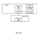
- FIG. 1B shows an example of a generic software architecture used by system 100 .
- Processor 104 executes an operating system 140 for controlling the overall operations of computing system 102 .
- the operating system may be Windows based, Linux operating system, Solaris, or any other operating system type.
- the embodiments disclosed herein are not limited to any particular operating system type.
- An application 142 may be executed by processor 104 for performing certain functions.
- application 142 may be an email program, a database application or any other application type.
- Application 142 may send a command to a driver 144 for performing an operation, for example, reading and/or writing data (input/output (I/O) at another storage device.
- the driver 144 processes the request and communicates with firmware 146 executed by processor 124 of adapter 116 .
- a component of adapter 116 then processes the request.
- an IOCB is first generated by the driver 144 and saved at an IOCB queue 148 , shown as 148 A- 148 N.
- the IOCB queue 148 may be at host memory 106 or any other location.
- the IOCB is obtained by adapter 116 , the purpose of which may be to provide data to host processor 104 or to send data provided by host processor 104 .
- an IOCB typically includes an “address” of host memory 106 where data that needs to be sent is stored and a “length” that indicates the amount of data that needs to be transferred. Both IOCB fetch and data transfer operations are performed using DMA operations via the DMA channels 168 A-N. Based on the IOCB, adapter 116 executes the operations that may be needed.
- Adapter 116 then uses a DMA operation to send a status block (IOSB) to processor 104 indicating the completion of IOCB execution and associated data transfer.
- the adapter 116 then sends an interrupt message to the host processor 104 to indicate completion of IOCB execution and posting of the IOSB status in the host system memory 106 so that it can process IOSBs and notify application 142 of the completion of the data transfer process
- FIG. 1C illustrates details of host interface 118 , according to one embodiment.
- Host interface 118 includes a plurality of modules which are configured to process PCI-Express packets.
- Host interface 118 may include a PCI-Express media access control (MAC) layer (also referred to as PHY or PHY layer) 150 A for receiving and sending messages via link 115 .
- Host interface 118 includes a PCI-Express data link layer (referred to as DLL) 150 B between a PCI-Express transaction layer (referred to as TL) 150 C and PHY 150 A.
- DLL PCI-Express data link layer
- TL PCI-Express transaction layer
- PHY 150 A, DLL 150 B and TL 150 C are defined by the PCI-Express specification.
- Host interface 118 also includes a PCI-Express Transaction Handler (PTH) 154 that interfaces with the DMA module 119 and TL 150 C to send and receive information via link 115 .
- PTH 154 performs various functions including error checking and others.
- PCI-Express uses a packet-based protocol to exchange information between TL 150 A and a TL (not shown) at the adapter interface 110 . Transactions are carried out using requests and completions. Completions are used only when required, for example, to return read data or to acknowledge completion of a request.
- packets On the transmit side (i.e. packets to processor 104 from adapter 116 ), packets flow from the TL 150 C to PHY 150 A.
- packets On the receive side (i.e. packets to adapter 116 from processor 104 ), packets are processed by the PHY layer 150 A and sent to TL 150 C for processing.
- TL 150 C assembles and disassembles Transaction Layer Packets (“TLPs”). TLPs are used to communicate transactions, such as read and write and other type of events.
- TLPs Transaction Layer Packets
- FIG. 1C shows more than one processor 124 (labeled as 124 A- 124 C) for adapter 116 .
- processors 124 A- 124 C interface with the DMA module 119 to send and receive data and messages via link 115 .
- driver 144 generates an IOCB for an I/O request to send data via network link 132 to a destination.
- the IOCB is placed at the IOCB queue 148 .
- the IOCB (for example, 156 A) is then received by adapter 116 and provided to one of the processors, for example, 124 A.
- the processor 124 A programs a DMA channel (for example, 168 A) to obtain data from host memory 106 via path 156 B. Once data is received it is transmitted via the network interface 130 and network link 132 to its destination.
- the PCI-Express Gen 3 (i.e. third generation) specification describes certain framing errors, which when detected may require a PCI-Express link to undergo a “re-training” sequence.
- the re-training sequence is also described by the PCI-Express standard specification. Re-training the link stops data transfer which slows down the bandwidth available to a PCI-Express link.
- a method and system are provided where certain framing errors that don't affect data transfer are ignored.
- Adapter 116 may also ignore certain framing errors that it keeps detecting because of a link partner but the errors do not result in data corruption.
- TLP Transfer Layer Packet
- STP Token a framing token that indicates the start of a TLP
- All DWs (data words) of a TLP are to be transmitted, even if the TLP is nullified.
- EDB Token End bad symbol that marks the end of a nullified TLP
- the value of the TLP Length field of a nullified TLP's STP Token is NOT adjusted to account for the EDB Token.
- the STP Token is not be transmitted more frequently than once per Symbol Time.
- DLLP data link layer packet
- SDP session description protocol
- Token defined by PCI-Express as having two symbols
- FIG. 2 shows a process 200 for managing framing errors, according to one embodiment.
- the process begins in block B 200 , when adapter 116 is initialized.
- the standard PCI-Express rules for re-transmission are enforced for sending and receiving information to processor 104 via link 115 .
- the firmware 146 of adapter 116 determines if certain framing errors occur due to defects at a link partner.
- link partner as used herein means a device communicating with another device via a link.
- adapter interface 110 and host interface 118 are link partners communicating via link 115 . Without these instructions, link 115 will be re-trained even though the framing error is benign.
- the adapter firmware determines if the framing error violations based on standard protocol rules are benign or may result in data corruption.
- the pre-load data structure 128 A is programmed to disable link training for those benign rule violations.
- the pre-load data structure 128 A is used to store instructions for firmware 146 to instruct the host interface 118 to disable re-training of link 115 .
- the re-training sequence is defined by the PCI-Express specification that is incorporated herein by reference.
- the pre-load data structure 128 A allows adapter 116 to perform a task that is typically performed by most PCI-Express devices.
Abstract
Description
Claims (20)
Priority Applications (1)
| Application Number | Priority Date | Filing Date | Title |
|---|---|---|---|
| US14/058,887 US9311268B1 (en) | 2012-10-25 | 2013-10-21 | Method and system for communication with peripheral devices |
Applications Claiming Priority (2)
| Application Number | Priority Date | Filing Date | Title |
|---|---|---|---|
| US201261718599P | 2012-10-25 | 2012-10-25 | |
| US14/058,887 US9311268B1 (en) | 2012-10-25 | 2013-10-21 | Method and system for communication with peripheral devices |
Publications (1)
| Publication Number | Publication Date |
|---|---|
| US9311268B1 true US9311268B1 (en) | 2016-04-12 |
Family
ID=55643203
Family Applications (1)
| Application Number | Title | Priority Date | Filing Date |
|---|---|---|---|
| US14/058,887 Active 2034-12-02 US9311268B1 (en) | 2012-10-25 | 2013-10-21 | Method and system for communication with peripheral devices |
Country Status (1)
| Country | Link |
|---|---|
| US (1) | US9311268B1 (en) |
Cited By (9)
| Publication number | Priority date | Publication date | Assignee | Title |
|---|---|---|---|---|
| US20150012774A1 (en) * | 2012-03-29 | 2015-01-08 | Fujitsu Limited | Information processing apparatus and method for controlling information processing apparatus |
| US20180254943A1 (en) * | 2017-03-01 | 2018-09-06 | Intel Corporation | Applying framing rules for a high speed data link |
| US11153032B2 (en) | 2017-02-28 | 2021-10-19 | Intel Corporation | Forward error correction mechanism for peripheral component interconnect-express (PCI-E) |
| WO2021236187A1 (en) * | 2020-05-21 | 2021-11-25 | Microsoft Technology Licensing, Llc | Improved error recovery and power management between nodes of an interconnection network |
| US11223446B2 (en) | 2018-12-18 | 2022-01-11 | Intel Corporation | Forward error correction mechanism for data transmission across multi-lane links |
| US11249837B2 (en) | 2019-03-01 | 2022-02-15 | Intel Corporation | Flit-based parallel-forward error correction and parity |
| US11296994B2 (en) | 2019-05-13 | 2022-04-05 | Intel Corporation | Ordered sets for high-speed interconnects |
| US11637657B2 (en) | 2019-02-15 | 2023-04-25 | Intel Corporation | Low-latency forward error correction for high-speed serial links |
| US11740958B2 (en) | 2019-11-27 | 2023-08-29 | Intel Corporation | Multi-protocol support on common physical layer |
Citations (6)
| Publication number | Priority date | Publication date | Assignee | Title |
|---|---|---|---|---|
| US20030131179A1 (en) * | 2001-08-24 | 2003-07-10 | Jasmin Ajanovic | General input/output architecture, protocol and related methods to provide isochronous channels |
| US6691192B2 (en) * | 2001-08-24 | 2004-02-10 | Intel Corporation | Enhanced general input/output architecture and related methods for establishing virtual channels therein |
| US7010607B1 (en) * | 1999-09-15 | 2006-03-07 | Hewlett-Packard Development Company, L.P. | Method for training a communication link between ports to correct for errors |
| US20090323722A1 (en) * | 2008-06-25 | 2009-12-31 | Debendra Das Sharma | Link and lane level packetization scheme of encoding in serial links |
| US20120317607A1 (en) * | 2011-06-10 | 2012-12-13 | David Wyatt | System and method for dynamically configuring a serial data link in a display device |
| US20130050216A1 (en) * | 2011-08-31 | 2013-02-28 | Colin Whitby-Strevens | Methods and apparatus for low power audio visual interface interoperability |
-
2013
- 2013-10-21 US US14/058,887 patent/US9311268B1/en active Active
Patent Citations (6)
| Publication number | Priority date | Publication date | Assignee | Title |
|---|---|---|---|---|
| US7010607B1 (en) * | 1999-09-15 | 2006-03-07 | Hewlett-Packard Development Company, L.P. | Method for training a communication link between ports to correct for errors |
| US20030131179A1 (en) * | 2001-08-24 | 2003-07-10 | Jasmin Ajanovic | General input/output architecture, protocol and related methods to provide isochronous channels |
| US6691192B2 (en) * | 2001-08-24 | 2004-02-10 | Intel Corporation | Enhanced general input/output architecture and related methods for establishing virtual channels therein |
| US20090323722A1 (en) * | 2008-06-25 | 2009-12-31 | Debendra Das Sharma | Link and lane level packetization scheme of encoding in serial links |
| US20120317607A1 (en) * | 2011-06-10 | 2012-12-13 | David Wyatt | System and method for dynamically configuring a serial data link in a display device |
| US20130050216A1 (en) * | 2011-08-31 | 2013-02-28 | Colin Whitby-Strevens | Methods and apparatus for low power audio visual interface interoperability |
Non-Patent Citations (6)
| Title |
|---|
| "PCI Express Base Specification Revision 3.0", PCI-SIG, (Nov. 10, 2010). |
| Boncelet, (The NTMAC for Authentication of Noisy Messages) Mar. 2006, IEEE Transactions on information forensics and security vol. 1 No. 1, p. 35-42. * |
| Chhaya, (Performance modeling of asynchronous data transfer methods of IEEE 802.11 MAC protocol*), 1997, Blatzer, Wireless Networks 3, p. 217-234. * |
| Haskell, (Resynchronization of Motion Compensated Video Affected by ATM Cell Loss), 1992, IEEE, p. 545-548. * |
| PCI Sig, (Errata for the PCI Express® Base Specification Revision 2.1) Nov. 2010, PCISIG, p. 1-76. * |
| Shah, (Keyboards and Covert Channels), Jun. 2006, Usenix, 15th Usenix Security Symposium (University of Pennsylvania), p. 59-75. * |
Cited By (13)
| Publication number | Priority date | Publication date | Assignee | Title |
|---|---|---|---|---|
| US20150012774A1 (en) * | 2012-03-29 | 2015-01-08 | Fujitsu Limited | Information processing apparatus and method for controlling information processing apparatus |
| US11153032B2 (en) | 2017-02-28 | 2021-10-19 | Intel Corporation | Forward error correction mechanism for peripheral component interconnect-express (PCI-E) |
| US20180254943A1 (en) * | 2017-03-01 | 2018-09-06 | Intel Corporation | Applying framing rules for a high speed data link |
| US10250436B2 (en) * | 2017-03-01 | 2019-04-02 | Intel Corporation | Applying framing rules for a high speed data link |
| US11223446B2 (en) | 2018-12-18 | 2022-01-11 | Intel Corporation | Forward error correction mechanism for data transmission across multi-lane links |
| US11637657B2 (en) | 2019-02-15 | 2023-04-25 | Intel Corporation | Low-latency forward error correction for high-speed serial links |
| US11249837B2 (en) | 2019-03-01 | 2022-02-15 | Intel Corporation | Flit-based parallel-forward error correction and parity |
| US11934261B2 (en) | 2019-03-01 | 2024-03-19 | Intel Corporation | Flit-based parallel-forward error correction and parity |
| US11296994B2 (en) | 2019-05-13 | 2022-04-05 | Intel Corporation | Ordered sets for high-speed interconnects |
| US11595318B2 (en) | 2019-05-13 | 2023-02-28 | Intel Corporation | Ordered sets for high-speed interconnects |
| US11740958B2 (en) | 2019-11-27 | 2023-08-29 | Intel Corporation | Multi-protocol support on common physical layer |
| US11502783B2 (en) | 2020-05-21 | 2022-11-15 | Microsoft Technology Licensing, Llc | Error recovery and power management between nodes of an interconnection network |
| WO2021236187A1 (en) * | 2020-05-21 | 2021-11-25 | Microsoft Technology Licensing, Llc | Improved error recovery and power management between nodes of an interconnection network |
Similar Documents
| Publication | Publication Date | Title |
|---|---|---|
| US9311268B1 (en) | Method and system for communication with peripheral devices | |
| JP5922268B2 (en) | Packet transmission using extension header | |
| US7937447B1 (en) | Communication between computer systems over an input/output (I/O) bus | |
| US7461195B1 (en) | Method and system for dynamically adjusting data transfer rates in PCI-express devices | |
| US7941569B2 (en) | Input/output tracing in a protocol offload system | |
| US20210055777A1 (en) | System power management in multi-port i/o hybrid systems | |
| KR102427550B1 (en) | QoS-AWARE IO MANAGEMENT FOR PCIe STORAGE SYSTEM WITH RECONFIGURABLE MULTI-PORTS | |
| US20070266186A1 (en) | Method and system for receiver detection in pci-express devices | |
| US20130086433A1 (en) | Providing Error Handling Support To Legacy Devices | |
| CN110557311B (en) | Inter-processor communication method for inter-die access latency in system-in-package | |
| WO2015131516A1 (en) | Distributed intelligent platform management bus connection method and atca frame | |
| US8677044B1 (en) | Method and system for communication using multiple DMA channels | |
| US7669190B2 (en) | Method and system for efficiently recording processor events in host bus adapters | |
| TW202248869A (en) | Peripheral component interconnect express interface device and operating method thereof | |
| US9720733B1 (en) | Methods and systems for control block routing | |
| US7802026B2 (en) | Method and system for processing frames in storage controllers | |
| US9588920B1 (en) | Method and system for port trunking | |
| US8978052B1 (en) | System and methods for inter-driver communication | |
| US8977786B1 (en) | Method and system for processing information at peripheral devices | |
| US9229791B1 (en) | System and method for high speed multiple buffer allocation | |
| JP4432388B2 (en) | I / O controller | |
| US10275261B1 (en) | Methods and systems for message logging and retrieval in computer systems | |
| US9172661B1 (en) | Method and system for using lane alignment markers | |
| US10020929B1 (en) | Methods and systems for data alignment in network devices | |
| US20060064531A1 (en) | Method and system for optimizing data transfer in networks |
Legal Events
| Date | Code | Title | Description |
|---|---|---|---|
| AS | Assignment |
Owner name: QLOGIC, CORPORATION, CALIFORNIA Free format text: ASSIGNMENT OF ASSIGNORS INTEREST;ASSIGNORS:CHEN, QIAN;WEIMER, RONALD A.;REEL/FRAME:031445/0270 Effective date: 20131014 |
|
| STCF | Information on status: patent grant |
Free format text: PATENTED CASE |
|
| AS | Assignment |
Owner name: JPMORGAN CHASE BANK, N.A., AS COLLATERAL AGENT, IL Free format text: SECURITY AGREEMENT;ASSIGNOR:QLOGIC CORPORATION;REEL/FRAME:041854/0119 Effective date: 20170228 |
|
| AS | Assignment |
Owner name: CAVIUM, INC., CALIFORNIA Free format text: MERGER;ASSIGNOR:QLOGIC CORPORATION;REEL/FRAME:044812/0504 Effective date: 20160615 |
|
| AS | Assignment |
Owner name: CAVIUM NETWORKS LLC, CALIFORNIA Free format text: RELEASE BY SECURED PARTY;ASSIGNOR:JP MORGAN CHASE BANK, N.A., AS COLLATERAL AGENT;REEL/FRAME:046496/0001 Effective date: 20180706 Owner name: CAVIUM, INC, CALIFORNIA Free format text: RELEASE BY SECURED PARTY;ASSIGNOR:JP MORGAN CHASE BANK, N.A., AS COLLATERAL AGENT;REEL/FRAME:046496/0001 Effective date: 20180706 Owner name: QLOGIC CORPORATION, CALIFORNIA Free format text: RELEASE BY SECURED PARTY;ASSIGNOR:JP MORGAN CHASE BANK, N.A., AS COLLATERAL AGENT;REEL/FRAME:046496/0001 Effective date: 20180706 |
|
| AS | Assignment |
Owner name: CAVIUM, LLC, CALIFORNIA Free format text: CHANGE OF NAME;ASSIGNOR:CAVIUM, INC.;REEL/FRAME:047205/0953 Effective date: 20180921 |
|
| MAFP | Maintenance fee payment |
Free format text: PAYMENT OF MAINTENANCE FEE, 4TH YEAR, LARGE ENTITY (ORIGINAL EVENT CODE: M1551); ENTITY STATUS OF PATENT OWNER: LARGE ENTITY Year of fee payment: 4 |
|
| AS | Assignment |
Owner name: CAVIUM INTERNATIONAL, CAYMAN ISLANDS Free format text: ASSIGNMENT OF ASSIGNORS INTEREST;ASSIGNOR:CAVIUM, LLC;REEL/FRAME:051948/0807 Effective date: 20191231 |
|
| AS | Assignment |
Owner name: MARVELL ASIA PTE, LTD., SINGAPORE Free format text: ASSIGNMENT OF ASSIGNORS INTEREST;ASSIGNOR:CAVIUM INTERNATIONAL;REEL/FRAME:053179/0320 Effective date: 20191231 |
|
| MAFP | Maintenance fee payment |
Free format text: PAYMENT OF MAINTENANCE FEE, 8TH YEAR, LARGE ENTITY (ORIGINAL EVENT CODE: M1552); ENTITY STATUS OF PATENT OWNER: LARGE ENTITY Year of fee payment: 8 |