US9324936B2 - Magnetic logic unit (MLU) cell and amplifier having a linear magnetic signal - Google Patents
Magnetic logic unit (MLU) cell and amplifier having a linear magnetic signal Download PDFInfo
- Publication number
- US9324936B2 US9324936B2 US14/431,140 US201314431140A US9324936B2 US 9324936 B2 US9324936 B2 US 9324936B2 US 201314431140 A US201314431140 A US 201314431140A US 9324936 B2 US9324936 B2 US 9324936B2
- Authority
- US
- United States
- Prior art keywords
- magnetic
- magnetization
- layer
- mlu
- biasing
- Prior art date
- Legal status (The legal status is an assumption and is not a legal conclusion. Google has not performed a legal analysis and makes no representation as to the accuracy of the status listed.)
- Active
Links
- 230000005291 magnetic effect Effects 0.000 title claims abstract description 214
- 230000005415 magnetization Effects 0.000 claims abstract description 91
- 230000004888 barrier function Effects 0.000 claims abstract description 28
- 230000003068 static effect Effects 0.000 claims abstract description 10
- 230000005290 antiferromagnetic effect Effects 0.000 claims description 13
- 239000000956 alloy Substances 0.000 claims description 6
- 229910045601 alloy Inorganic materials 0.000 claims description 6
- 229910003321 CoFe Inorganic materials 0.000 claims description 4
- 229910000684 Cobalt-chrome Inorganic materials 0.000 claims description 2
- 229910005335 FePt Inorganic materials 0.000 claims description 2
- 229910019041 PtMn Inorganic materials 0.000 claims description 2
- 239000010952 cobalt-chrome Substances 0.000 claims description 2
- 230000004044 response Effects 0.000 description 10
- 230000008878 coupling Effects 0.000 description 8
- 238000010168 coupling process Methods 0.000 description 8
- 238000005859 coupling reaction Methods 0.000 description 8
- 230000005294 ferromagnetic effect Effects 0.000 description 6
- 230000006870 function Effects 0.000 description 5
- 229910019236 CoFeB Inorganic materials 0.000 description 4
- 238000000034 method Methods 0.000 description 3
- 230000008569 process Effects 0.000 description 3
- 238000003860 storage Methods 0.000 description 3
- 239000000758 substrate Substances 0.000 description 3
- 238000000137 annealing Methods 0.000 description 2
- 238000005516 engineering process Methods 0.000 description 2
- 238000010438 heat treatment Methods 0.000 description 2
- ZOXJGFHDIHLPTG-UHFFFAOYSA-N Boron Chemical compound [B] ZOXJGFHDIHLPTG-UHFFFAOYSA-N 0.000 description 1
- 101100422538 Escherichia coli sat-2 gene Proteins 0.000 description 1
- WYTGDNHDOZPMIW-RCBQFDQVSA-N alstonine Natural products C1=CC2=C3C=CC=CC3=NC2=C2N1C[C@H]1[C@H](C)OC=C(C(=O)OC)[C@H]1C2 WYTGDNHDOZPMIW-RCBQFDQVSA-N 0.000 description 1
- 230000003321 amplification Effects 0.000 description 1
- 239000002885 antiferromagnetic material Substances 0.000 description 1
- 230000006399 behavior Effects 0.000 description 1
- 230000008901 benefit Effects 0.000 description 1
- 230000015572 biosynthetic process Effects 0.000 description 1
- 230000000903 blocking effect Effects 0.000 description 1
- 229910052796 boron Inorganic materials 0.000 description 1
- 238000005253 cladding Methods 0.000 description 1
- 230000000694 effects Effects 0.000 description 1
- 229910052735 hafnium Inorganic materials 0.000 description 1
- 239000000696 magnetic material Substances 0.000 description 1
- 238000004519 manufacturing process Methods 0.000 description 1
- 230000000873 masking effect Effects 0.000 description 1
- 239000000463 material Substances 0.000 description 1
- 229910052758 niobium Inorganic materials 0.000 description 1
- 238000003199 nucleic acid amplification method Methods 0.000 description 1
- 230000000737 periodic effect Effects 0.000 description 1
- 229910052715 tantalum Inorganic materials 0.000 description 1
- GUVRBAGPIYLISA-UHFFFAOYSA-N tantalum atom Chemical compound [Ta] GUVRBAGPIYLISA-UHFFFAOYSA-N 0.000 description 1
- 229910052719 titanium Inorganic materials 0.000 description 1
- 229910052726 zirconium Inorganic materials 0.000 description 1
Images


Classifications
-
- H—ELECTRICITY
- H10—SEMICONDUCTOR DEVICES; ELECTRIC SOLID-STATE DEVICES NOT OTHERWISE PROVIDED FOR
- H10N—ELECTRIC SOLID-STATE DEVICES NOT OTHERWISE PROVIDED FOR
- H10N50/00—Galvanomagnetic devices
- H10N50/80—Constructional details
-
- H01L43/02—
-
- G—PHYSICS
- G11—INFORMATION STORAGE
- G11C—STATIC STORES
- G11C11/00—Digital stores characterised by the use of particular electric or magnetic storage elements; Storage elements therefor
- G11C11/02—Digital stores characterised by the use of particular electric or magnetic storage elements; Storage elements therefor using magnetic elements
- G11C11/16—Digital stores characterised by the use of particular electric or magnetic storage elements; Storage elements therefor using magnetic elements using elements in which the storage effect is based on magnetic spin effect
- G11C11/165—Auxiliary circuits
- G11C11/1675—Writing or programming circuits or methods
-
- H01L43/10—
-
- H—ELECTRICITY
- H03—ELECTRONIC CIRCUITRY
- H03F—AMPLIFIERS
- H03F15/00—Amplifiers using galvano-magnetic effects not involving mechanical movement, e.g. using Hall effect
-
- H—ELECTRICITY
- H03—ELECTRONIC CIRCUITRY
- H03K—PULSE TECHNIQUE
- H03K19/00—Logic circuits, i.e. having at least two inputs acting on one output; Inverting circuits
- H03K19/02—Logic circuits, i.e. having at least two inputs acting on one output; Inverting circuits using specified components
- H03K19/18—Logic circuits, i.e. having at least two inputs acting on one output; Inverting circuits using specified components using galvano-magnetic devices, e.g. Hall-effect devices
-
- H—ELECTRICITY
- H10—SEMICONDUCTOR DEVICES; ELECTRIC SOLID-STATE DEVICES NOT OTHERWISE PROVIDED FOR
- H10N—ELECTRIC SOLID-STATE DEVICES NOT OTHERWISE PROVIDED FOR
- H10N50/00—Galvanomagnetic devices
- H10N50/80—Constructional details
- H10N50/85—Magnetic active materials
Definitions
- the present invention concerns a magnetic logic unit (MLU) cell based on MRAM technology having a linear magnetic signal.
- MLU magnetic logic unit
- the present invention further concerns a MLU amplifier comprising a plurality of the MLU cell.
- a conventional MRAM cell comprises a magnetic tunnel junction comprising a ferromagnetic reference layer and a ferromagnetic storage layer.
- the resistance of the stack is low, this could be a “0” (or arbitrarily a “1”).
- the layers are anti-aligned the resistance is high, this could be a “1” (or vice versa).
- TAS MRAM thermally-assisted-switching
- the storage layer is blocked by an antiferromagnetic layer such as to achieve superior stability in normal operating temperatures.
- the temperature of the cell is momentarily locally raised above a blocking temperature of the antiferromagnetic layer, through resistive heating of the magnetic tunnel junction, allowing the magnetoresistance of the TAS-MRAM cell to be varied.
- the information stored in TAS-MRAM memory cells is thus not affected by external fields and noise.
- Self-referenced MRAM cells can be based on TAS MRAM cells.
- Self-referenced MRAM cells typically have the reference layer that is not pinned by an antiferromagnetic layer but is free to be varied. Such unpinned reference layer is often called “sense layer”.
- sense layer When a current is applied in a field line adjacent to the MRAM cell, a magnetic field is generated such as to vary the sense layer magnetization during a read operation.
- a two-phase read operation utilizes the natural tendency of an un-driven field line's effect on a selected memory cell to create a momentary reference value that is compared to the cell's value when the field is driven. The stored information is thus read as this field is applied.
- MRAM magnetic random access memory
- a magnetic logic unit (MLU) cell is built on the self-referenced TAS MRAM technology. During logic operations the field lines are acting as controlling gates modulating the resistivity of the magnetic tunnel junction.
- the MLU cell behaves as a three-terminal device capable of performing native logical functions. The currents circulating in the field line can be modulated in direction, and intensity.
- a MLU amplifier can be provided by electrically coupling an array comprising several (possibly tens of thousands) of MLU cells together.
- the gain of the resulting amplifier is largely increased device while the coupling capacitance remains very small.
- the magnetoresistance of the magnetic tunnel junction is modulated by the direction of a field current flowing through a field line which is set by an input bit to be matched.
- a high or low magnetoresistance at the output indicates whether the input bit matches the stored bit or not, respectively.
- N the total number of magnetic tunnel junctions in the array
- P mtj the power delivered by a single magnetic tunnel junction.
- the MLU amplifier is an active device that can be built without any CMOS substrate. Consequently, a low cost five mask process on a bare substrate can be appropriate to manufacture such MLU amplifier. Only two extra masking processes on a standard CMOS process will enable System On a Chip capability that integrates MLU amplifier solutions.
- FIG. 1 shows an output voltage and an output current generated by the MLU amplifier upon passing an input current in a current line electrically connecting in series the plurality of MLU cells.
- the input current need to be set at the cutoff level where the output impedance is in the middle of the potential excursion to deliver the highest gain.
- the AC signal at the input stage will create large resistance variations in the output stage, creating a large output signal.
- class A For linear amplification, class A, this current needs to be adjusted to the particular point where slope of the IV curve is the highest.
- class C the input set up will be where the DC power is at its minimum (all magnetic tunnel junctions having their storage and sense magnetization parallel).
- the output of the MLU cell and of the MLU amplifier can be determined by a hysteresis loop reporting the applied magnetic field against the magnetization of the MLU cell(s).
- the presence of a large hysteresis curve will prevent the MLU amplifier to operate on a class C mode, and will require at least a full 1 mA input peak current swing to operate class C.
- the present disclosure concerns a magnetic logic unit (MLU) cell comprising: a first magnetic tunnel junction and a second magnetic tunnel junction, each magnetic tunnel junction comprising a first ferromagnetic layer having a first magnetization, a second ferromagnetic layer having a second magnetization, and a barrier layer between the first and second ferromagnetic layers; a strap, electrically connecting the magnetic tunnel junction in series with the second magnetic tunnel junction; and a field line for passing a field current such as to generate an external magnetic field adapted to adjust the first magnetization; the first and second ferromagnetic layers and the barrier layer being arranged such that the first magnetization is magnetically coupled antiparallel with the second magnetization through the barrier layer; the MLU cell further comprising a biasing device arranged for applying a static biasing magnetic field oriented substantially parallel to the external magnetic field such as to orient the first magnetization at about 90° relative to the second magnetization, the first and second magnetizations being oriented symmetrically relative to the direction of the external magnetic field.
- the present disclosure also concerns an MLU amplifier comprising a plurality of the MLU cell.
- the disclosed MLU amplifier has large gains and extended cut off frequencies.
- the MLU amplifier maximizes the linearity and/or the TMR.
- FIG. 1 represents an output voltage and an output current generated by a MLU amplifier
- FIG. 2 a shows a cross section view of a magnetic logic unit (MLU) cell comprising two magnetic tunnel junctions, each magnetic tunnel junction comprising a first magnetic layer separated from a second magnetic layer by a barrier layer;
- MLU magnetic logic unit
- FIG. 2 b shows a top view of a magnetic logic unit (MLU) cell comprising two magnetic tunnel junctions, each magnetic tunnel junction comprising a first magnetic layer separated from a second magnetic layer by a barrier layer;
- MLU magnetic logic unit
- FIG. 3 illustrates one of the magnetic tunnel junctions of the MLU cell, according to an embodiment
- FIG. 4 shows the orientation of magnetic moment of the two magnetic layers in the presence of a magnetic field
- FIG. 5 shows the magnetization response of the tunnel magnetic junction as a function of the magnetic field
- FIG. 6 illustrates the tunnel magnetoresistance response as a function of the magnetic field
- FIG. 7 shows the tunnel magnetoresistance response for the two magnetic layers coupled through the barrier layer
- FIGS. 8 a and b illustrates one of the magnetic tunnel junctions of the MLU cell, according to two other embodiments.
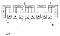
- FIG. 9 shows a MLU amplifier comprising a plurality of MLU cells electrically connected in series.
- FIG. 2 shows a cross section view (a) and a top view (b) of an MLU cell 1 according to an embodiment.
- the MLU cell 1 comprises a first and second magnetic tunnel junction 2 , each of the two magnetic tunnel junctions 2 being electrically connected in series at one end via an electrically conductive strap 7 .
- a current line 3 is electrically connected to the other end of the magnetic tunnel junctions 2 .
- the current line 3 can be used to pass a heating current during a write operation or a read current during a read operation.
- the MLU cell 1 further comprises a field line 4 arranged for passing a field current 41 such as to generate an external magnetic field 42 .
- the field line 4 is represented as two parallel field line portions 4 ′ located at the end of the magnetic tunnel junctions 2 connecting the strap 7 .
- the field line 4 (or each of the field line portions 4 ′) can preferably comprise a cladding.
- FIG. 3 illustrates one of the magnetic tunnel junctions 2 of the MLU cell 1 , according to an embodiment.
- the magnetic tunnel junction 2 includes a first magnetic layer 21 having a first magnetization 210 and a second magnetic layer 23 having a second magnetization 230 , and a barrier layer 22 between the first and second magnetic layer 21 , 23 .
- the magnetic tunnel junction 2 is arranged such as to behave as a pseudo spin valve, wherein the first magnetization 210 is magnetically coupled antiparallel with the second magnetization 230 through the barrier layer 22 .
- the magnetic tunnel junction 2 further comprises a non-magnetic layer 24 in contact with the side of the first magnetic layer 21 opposed to the one contacting the barrier layer 22 , and another non-magnetic layer 24 in contact with the side of the second magnetic layer 23 opposed to the one contacting the barrier layer 22 .
- the non-magnetic layer 24 can comprise tantalum.
- the first layer 21 is arranged such that the magnetic tunnel junction magnetization varies linearly with the generated external magnetic field 42 .
- the barrier layer 22 is non-magnetic and preferably comprises an MgO oxide.
- the barrier layer 22 has a thickness typically comprised between about 1 nm and 10 nm.
- the magnetic tunnel junction can further comprise a thin MgO layer at the interface, or in the vicinity of the interface, between the non-magnetic layer 24 and the first and/or second magnetic layer 21 , 23 .
- the thin MgO layer allows increasing thermal stability of the magnetic tunnel junction 2 upon high temperature annealing.
- the magnetic tunnel junction 2 comprising the thin MgO layer can withstand an annealing at a temperature larger than 400° C. and provide very large tunnel magnetoresistance (TMR) ranging between about 400% and 500%.
- TMR tunnel magnetoresistance
- the first and second magnetic layer 21 , 23 preferably comprise a CoFeB alloy.
- the two magnetic layers 21 , 23 should be thick enough such as to increase the magnetic susceptibility of the magnetic tunnel junction 2 and lower the field are required to generate the TMR signal.
- the thickness should however not be too thick in order to avoid getting a vortex micromagnetic configuration in the magnetic layers 21 , 23 .
- the magnetic layers 21 , 23 can have a thickness typically comprised between about 1.5 nm and about 4 nm.
- each of the two magnetic layers 21 , 23 can be formed from a multilayer comprising a sequence of two magnetic layers separated by an intermediate layer comprising an element from at least one of a Group IIIB and Group IVB of the periodic table.
- the multilayers can comprise a sequence such as CoFe/Ta/CoFeB as bottom electrode (on the side of the field line 4 ), wherein one of the CoFeB layer is in contact with the barrier layer 22 .
- the Ta layer plays the role of a boron getter layer.
- the Ta intermediate layer can be replaced by an intermediate layer comprising Ti, Hf, Zr or Nb. In any case, the intermediate layer should be thin enough to insure good magnetic coupling between CoFe and CoFeB.
- the intermediate layer can comprise a sequence of layers such as Ta/Ru/Ta.
- the first and second magnetic layer 21 , 23 comprise materials having high Curie temperature, i.e., large stiffness constant such as to hinder formation of the vortex micromagnetic configuration.
- the conditions for having a quasi macrospin behavior in a cylindrical magnetic layer of thickness L and radius R are known.
- the configuration of the magnetization 210 , 230 should be in a leaf state.
- Magnetostatic coupling energy E MS between the two magnetic layers 21 , 23 in the configuration of FIG. 3 can be expressed in macrospin approximation with Equation 2:
- M 1 and M 2 are the magnetic moment of the two magnetic layers 21 , 23 being proportional to their magnetization 210 , 230 and the volume of each of the layers 21 , 23
- ⁇ o is the magnetic constant
- A is a characteristics surface area
- d is the distance between the two moments M 1 and M 2 .
- the magnetostatic energy has the same functional form as an antiferromagnetic coupling through the MgO barrier layer 22 .
- Equation ⁇ ⁇ 5 the magnetization response M(H) as a function of the magnetic field can be expressed by Equation 6 (see FIG. 5 ):
- Equation 7 The tunnel magnetoresistance response R(H) as a function of the magnetic field can be obtained by Equation 7:
- Equation 7 is equivalent to:
- This biasing can be achieved by applying a static biasing magnetic field H bias on the magnetic tunnel junction 2 being of the order of:
- H bias H sat 2 , ( Equation ⁇ ⁇ 9 ) where H sat is the saturation magnetic field.
- H sat the saturation magnetic field.
- FIG. 5 illustrates the first magnetoresistance 210 (indicated by symbol ⁇ right arrow over (M) ⁇ 1 ) and the second magnetoresistance 230 (indicated by symbol ⁇ right arrow over (M) ⁇ 2 ) being oriented with an angle ⁇ 1 and ⁇ 2 , respectively, with respect to the biasing magnetic field H bias .
- FIG. 7 shows an example of the tunnel magnetoresistance response R(H) for an first magnetization magnetically coupled antiparallel with a second magnetization through a barrier layer, such as in the magnetic tunnel junction 2 of FIG. 3 .
- the point indicated by numeral 54 corresponds to the bias point, i.e., the magnetoresistance response in the presence of the biasing magnetic field H bias .
- R min corresponds to the magnetoresistance of the magnetic tunnel junction 2 when the first and second magnetizations 210 , 230 are parallel
- R max corresponds to the magnetoresistance when the first and second magnetizations 210 , 230 are antiparallel.
- the MLU cell 1 further comprises a biasing device 50 arranged for applying a static biasing magnetic field 53 (corresponding to the biasing magnetic field H bias ) that is oriented substantially parallel to the external magnetic field 42 generated by the field line 4 and substantially perpendicular to the field line 4 .
- the static biasing magnetic field 53 applied by the bias device 50 is such as to orient the first magnetization 210 at about 90° relative to the second magnetization 230 , the first and second magnetizations being oriented symmetrically relative to the direction of the external magnetic field 42 .
- the first magnetization 210 is oriented with an angle of about 45° relative to the direction of the external magnetic field 42 and the second magnetization 230 is oriented with an angle of about ⁇ 45° relative to the direction of the external magnetic field 42 (see FIG. 2 b ).
- Applying the external magnetic field 42 by passing the field current 41 in the field line 4 moves further the first magnetization 210 relative to the second magnetization 230 towards an angle ⁇ of 0°, where the first and second magnetizations 210 , 230 are substantially parallel, or an angle ⁇ of 180° where the first and second magnetizations 210 , 230 are substantially antiparallel, depending on the direction of the external magnetic field 42 .
- the external magnetic field 42 is oriented in the same direction as the biasing magnetic field 53 (as shown in FIG.
- the first magnetizations 210 is oriented with an angle of angle ⁇ of about 0° relative to the second magnetization 230 , whereas in the case the external magnetic field 42 is oriented in a direction opposed to the one of the biasing magnetic field 53 , the first magnetization 210 is oriented with an angle of angle ⁇ of about 180° relative to the second magnetization 230 .
- the moving of the second magnetization 230 relative to the first magnetization 210 is caused by the magnetic coupling between the first and second magnetization 210 , 230 through the barrier layer 22 .
- the biasing device comprises a permanent magnet 50 arranged for applying the static biasing magnetic field 53 .
- the magnet 50 can be located at one end of the magnetic tunnel junction 2 on the side of the field line 4 , as shown in the example of FIG. 3 , or at the other end of the magnetic tunnel junction 2 .
- An advantage of this configuration is that the magnetic tunnel junction 2 can be annealed up to 520° C. yielding a TMR of up to 600%.
- the biasing device comprises a biasing layer 51 included in the magnetic tunnel junction 2 .
- the biasing layer 51 is arranged for generating the biasing magnetic field 53 being oriented substantially parallel to the external magnetic field 42 such as to orient the first magnetization 210 at about 90° relative to the second magnetization 230 , the first and second magnetizations being oriented symmetrically relative to the direction of the external magnetic field 42 .
- Applying the external magnetic field 42 by passing the field current 41 in the field line 4 moves further the first magnetization 210 relative to the second magnetization 230 towards an angle ⁇ of 0°, where the first and second magnetizations 210 , 230 are substantially parallel, or an angle ⁇ of 180° where the first and second magnetizations 210 , 230 are substantially antiparallel, depending on the direction of the external magnetic field 42 .
- the biasing layer 51 comprises a permanent magnet.
- the biasing layer 51 can comprise a FePt or a CoCr alloy.
- the biasing layer 51 comprises an exchange biased pinned layer comprising a third magnetic layer 511 and an antiferromagnetic layer 512 .
- the antiferromagnetic layer 512 exchange-couples the third magnetic layer 511 such that a magnetization of the magnetic layer 511 , or biasing magnetic field 53 , is oriented substantially parallel to the external magnetic field 42 such as to orient the first magnetization 210 at about 90° relative to the second magnetization 230 , the first and second magnetizations being oriented symmetrically relative to the direction of the external magnetic field 42 .
- the magnetic layer 511 can comprise a magnetic material such as CoFe and the antiferromagnetic layer 512 can comprise an antiferromagnetic material such as a PtMn alloy.
- the biasing layer 51 can be formed from a plurality of a multilayer comprising the magnetic layer 511 and antiferromagnetic layer 512 .
- the number of multilayers can be such as to obtain a predetermined magnitude of the biasing magnetic field 53 , for example being adequate for orienting the first magnetization 210 at about 90° relative to the second magnetization 230 , the first and second magnetizations being oriented symmetrically relative to the direction of the external magnetic field 42 .
- the biasing layer 51 is separated from the two magnetic layers 21 , 23 with the non-magnetic layer 24 .
- the biasing layer 51 can be on the side of the first magnetic layer 21 ( FIG. 8 a ) or of the second magnetic layer 23 ( FIG. 8 b ).
- FIG. 9 shows an MLU amplifier comprising a plurality of MLU cells 1 disclosed herein, the MLU cells 1 being electrically connected in series via the current line 3 .
- the magnetic tunnel junctions of the plurality of MLU cells are all connected in series with each other via the current line 3 and the strap 7 . Such configuration allows for increasing the output signal and the current gain.
- the plurality of MLU cells is electrically connected in series in a way such as to avoid contact to the substrate.
- the field lines 4 of each MLU cell are electrically connected in series such as to form a continuous field line 4 in the array.
- the field line 4 can take the shape of a serpentine.
Abstract
Description
P out =N×P mtj (Equation 1),
where N is the total number of magnetic tunnel junctions in the array, and Pmtj the power delivered by a single magnetic tunnel junction. Considering that each MLU cell is very small, for example down to 100 nm, the total output power can be high in an array comprising a millions of magnetic tunnel junctions. Moreover, the MLU amplifier is an active device that can be built without any CMOS substrate. Consequently, a low cost five mask process on a bare substrate can be appropriate to manufacture such MLU amplifier. Only two extra masking processes on a standard CMOS process will enable System On a Chip capability that integrates MLU amplifier solutions.
where M1 and M2 are the magnetic moment of the two
d=t MgO+½t F1+½t F2 (Equation 3),
where tMgO is the thickness of the
E=−μ 0 {right arrow over (M)} 1 ·{right arrow over (H)}−μ 0 {right arrow over (M)} 2 ·{right arrow over (H)}+A{right arrow over (M)} 1 ·{right arrow over (M)} 2 (Equation 4).
where θ1 and θ2 is the angle between the direction of the magnetic field and the first and
where Msat is the saturation magnetization.
where Rmin is the tunnel magnetic junction resistance when the first and second magnetizations are parallel, ΔR is and where Δθ=θ1−θ2.
where Rmax is the tunnel magnetic junction resistance when the first and second magnetizations are antiparallel.
where Hsat is the saturation magnetic field. In other words, the biasing magnetic field Hbias is such as to orient the
- 1 MLU cell
- 10 MLU amplifier
- 2 first magnetic tunnel junction
- 2′ second magnetic tunnel junction
- 21 first magnetic layer
- 210 first magnetization
- 22 barrier layer
- 23 second magnetic layer
- 230 second magnetization
- 24 non-magnetic layer
- 3 current line
- 4 field line
- 41 field current
- 42 magnetic field
- 50 biasing device, permanent magnet
- 51 biasing layer
- 511 third magnetic layer
- 512 antiferromagnetic layer
- 53 biasing magnetic field
- 54 bias point
- 7 strap
- A Characteristics surface area
- d distance d between the two moments M1 and M2
- E total energy
- EMS magnetostatic coupling energy
- H magnetic field
- Hbias biasing magnetic field
- HSAT saturation magnetic field
- M(H) magnetization response
- M1 magnetic moment of first magnetic layer
- M2 magnetic moment of second magnetic layer
- MSAT saturation magnetization
- Pout output power
- Pmtj power delivered by a magnetic tunnel junction
- N number of magnetic tunnel junctions
- Rmin minimum magnetoresistance
- Rmax maximum magnetoresistance
- tMgO barrier layer thickness
- tF1 thickness of first magnetic layer
- tF2 thickness of second magnetic layer
- θ1 angle between magnetic field and first magnetization
- θ2 angle between magnetic field and second magnetization
- μo magnetic constant
Claims (10)
Applications Claiming Priority (4)
| Application Number | Priority Date | Filing Date | Title |
|---|---|---|---|
| EP12290316.4 | 2012-09-25 | ||
| EP12290316 | 2012-09-25 | ||
| EP12290316.4A EP2712079B1 (en) | 2012-09-25 | 2012-09-25 | Magnetic logic unit (MLU) cell and amplifier having a linear magnetic signal |
| PCT/EP2013/068866 WO2014048757A1 (en) | 2012-09-25 | 2013-09-12 | Magnetic logic unit (mlu) cell and amplifier having a linear magnetic signal |
Publications (2)
| Publication Number | Publication Date |
|---|---|
| US20150270479A1 US20150270479A1 (en) | 2015-09-24 |
| US9324936B2 true US9324936B2 (en) | 2016-04-26 |
Family
ID=47522359
Family Applications (1)
| Application Number | Title | Priority Date | Filing Date |
|---|---|---|---|
| US14/431,140 Active US9324936B2 (en) | 2012-09-25 | 2013-09-12 | Magnetic logic unit (MLU) cell and amplifier having a linear magnetic signal |
Country Status (3)
| Country | Link |
|---|---|
| US (1) | US9324936B2 (en) |
| EP (1) | EP2712079B1 (en) |
| WO (1) | WO2014048757A1 (en) |
Families Citing this family (4)
| Publication number | Priority date | Publication date | Assignee | Title |
|---|---|---|---|---|
| US10297300B2 (en) | 2014-09-21 | 2019-05-21 | Samsung Electronics Co., Ltd. | Method and system for determining temperature using a magnetic junction |
| EP3002759B1 (en) | 2014-10-03 | 2020-08-05 | Crocus Technology S.A. | Method for writing in a magnetic device |
| EP3023803B1 (en) | 2014-11-19 | 2020-03-18 | Crocus Technology S.A. | MLU cell for sensing an external magnetic field and a magnetic sensor device comprising the MLU cell |
| CN112259139B (en) * | 2019-07-22 | 2022-09-30 | 中电海康集团有限公司 | Memory cell, memory, and method for initializing memory |
Citations (8)
| Publication number | Priority date | Publication date | Assignee | Title |
|---|---|---|---|---|
| US6259586B1 (en) | 1999-09-02 | 2001-07-10 | International Business Machines Corporation | Magnetic tunnel junction sensor with AP-coupled free layer |
| US6356147B1 (en) | 2000-12-19 | 2002-03-12 | International Business Machines Corporation | Wideband dual amplifier circuits |
| US20050216244A1 (en) | 2004-03-23 | 2005-09-29 | Nahas Joseph J | Magnetoresistive random access memory simulation |
| JP2006253562A (en) | 2005-03-14 | 2006-09-21 | Mitsubishi Electric Corp | Magneto-resistance effect element, magnetic field detector using the same, and method for manufacturing magneto-resistance effect element |
| US7196882B2 (en) * | 2002-07-23 | 2007-03-27 | Micron Technology, Inc. | Magnetic tunnel junction device and its method of fabrication |
| US7477490B2 (en) * | 2004-06-30 | 2009-01-13 | Seagate Technology Llc | Single sensor element that is naturally differentiated |
| US20100193890A1 (en) | 2007-08-03 | 2010-08-05 | Tetsuhiro Suzuki | Magnetic domain wall random access memory |
| US20120088125A1 (en) | 2009-03-27 | 2012-04-12 | National University Corporation Tohoku University | Magnetoresistive element and magnetic memory |
-
2012
- 2012-09-25 EP EP12290316.4A patent/EP2712079B1/en active Active
-
2013
- 2013-09-12 US US14/431,140 patent/US9324936B2/en active Active
- 2013-09-12 WO PCT/EP2013/068866 patent/WO2014048757A1/en active Application Filing
Patent Citations (8)
| Publication number | Priority date | Publication date | Assignee | Title |
|---|---|---|---|---|
| US6259586B1 (en) | 1999-09-02 | 2001-07-10 | International Business Machines Corporation | Magnetic tunnel junction sensor with AP-coupled free layer |
| US6356147B1 (en) | 2000-12-19 | 2002-03-12 | International Business Machines Corporation | Wideband dual amplifier circuits |
| US7196882B2 (en) * | 2002-07-23 | 2007-03-27 | Micron Technology, Inc. | Magnetic tunnel junction device and its method of fabrication |
| US20050216244A1 (en) | 2004-03-23 | 2005-09-29 | Nahas Joseph J | Magnetoresistive random access memory simulation |
| US7477490B2 (en) * | 2004-06-30 | 2009-01-13 | Seagate Technology Llc | Single sensor element that is naturally differentiated |
| JP2006253562A (en) | 2005-03-14 | 2006-09-21 | Mitsubishi Electric Corp | Magneto-resistance effect element, magnetic field detector using the same, and method for manufacturing magneto-resistance effect element |
| US20100193890A1 (en) | 2007-08-03 | 2010-08-05 | Tetsuhiro Suzuki | Magnetic domain wall random access memory |
| US20120088125A1 (en) | 2009-03-27 | 2012-04-12 | National University Corporation Tohoku University | Magnetoresistive element and magnetic memory |
Non-Patent Citations (2)
| Title |
|---|
| International Search Report for PCT/EP2013/068866 dated Oct. 7, 2013. |
| Written Opinion for PCT/EP2013/068866 dated Oct. 7, 2013. |
Also Published As
| Publication number | Publication date |
|---|---|
| EP2712079B1 (en) | 2015-06-03 |
| US20150270479A1 (en) | 2015-09-24 |
| EP2712079A1 (en) | 2014-03-26 |
| WO2014048757A1 (en) | 2014-04-03 |
Similar Documents
| Publication | Publication Date | Title |
|---|---|---|
| US8350347B2 (en) | Writable magnetic element | |
| US8482968B2 (en) | Non-volatile magnetic tunnel junction transistor | |
| US8416618B2 (en) | Writable magnetic memory element | |
| US6285581B1 (en) | MRAM having semiconductor device integrated therein | |
| RU2595588C2 (en) | Magnetic recording element | |
| US9395210B2 (en) | Magnetic logic units configured to measure magnetic field direction | |
| US7957179B2 (en) | Magnetic shielding in magnetic multilayer structures | |
| US9983275B2 (en) | Method for measuring three-dimensional magnetic fields | |
| US9989599B2 (en) | Magnetic sensor cell for measuring three-dimensional magnetic fields | |
| US20170372761A1 (en) | Systems for Source Line Sensing of Magnetoelectric Junctions | |
| EP2539896B1 (en) | A high gmr structure with low drive fields | |
| US9583695B2 (en) | Magnetic logic unit (MLU) cell and amplifier having a linear magnetic signal | |
| US9324936B2 (en) | Magnetic logic unit (MLU) cell and amplifier having a linear magnetic signal | |
| US20100053822A1 (en) | Stram cells with ampere field assisted switching | |
| US9276197B2 (en) | Hybrid domain wall-hall cross device | |
| EP2815401B1 (en) | Magnetic logic units configured as an amplifier | |
| US9689936B2 (en) | Apparatus and method for sensing a magnetic field using subarrays of magnetic sensing elements | |
| US9766305B2 (en) | Apparatus and method for layout of magnetic field sensing elements in sensors | |
| US9702944B2 (en) | Apparatus and method for sensing a magnetic field using arrays of magnetic sensing elements | |
| US20160018483A1 (en) | Apparatus, System, and Method for Sensing Communication Signals with Magnetic Field Sensing Elements | |
| JP2001217479A (en) | Magnetic tunnel junction element and magnetic memory using the same | |
| WO2005067052A1 (en) | Magnetic memory cell and magnetic memory device |
Legal Events
| Date | Code | Title | Description |
|---|---|---|---|
| AS | Assignment |
Owner name: CROCUS TECHNOLOGY SA, FRANCE Free format text: ASSIGNMENT OF ASSIGNORS INTEREST;ASSIGNORS:PREJBEANU, IOAN LUCIAN;DIENY, BERNARD;MACKAY, KENNETH;AND OTHERS;SIGNING DATES FROM 20150526 TO 20150621;REEL/FRAME:036077/0353 |
|
| FEPP | Fee payment procedure |
Free format text: PAYOR NUMBER ASSIGNED (ORIGINAL EVENT CODE: ASPN); ENTITY STATUS OF PATENT OWNER: SMALL ENTITY |
|
| STCF | Information on status: patent grant |
Free format text: PATENTED CASE |
|
| AS | Assignment |
Owner name: LLC "SBERBANK INVESTMENTS", RUSSIAN FEDERATION Free format text: SECURITY INTEREST;ASSIGNOR:CROCUS TECHNOLOGY, INC.;REEL/FRAME:045938/0810 Effective date: 20180314 |
|
| MAFP | Maintenance fee payment |
Free format text: PAYMENT OF MAINTENANCE FEE, 4TH YR, SMALL ENTITY (ORIGINAL EVENT CODE: M2551); ENTITY STATUS OF PATENT OWNER: SMALL ENTITY Year of fee payment: 4 |
|
| AS | Assignment |
Owner name: CROCUS TECHNOLOGY SA, FRANCE Free format text: CHANGE OF ADDRESS;ASSIGNOR:CROCUS TECHNOLOGY SA;REEL/FRAME:064658/0730 Effective date: 20180529 |
|
| AS | Assignment |
Owner name: CROCUS TECHNOLOGY, INC., FRANCE Free format text: RELEASE BY SECURED PARTY;ASSIGNOR:LLC "SBERBANK INVESTMENTS";REEL/FRAME:064783/0420 Effective date: 20220412 |
|
| MAFP | Maintenance fee payment |
Free format text: PAYMENT OF MAINTENANCE FEE, 8TH YR, SMALL ENTITY (ORIGINAL EVENT CODE: M2552); ENTITY STATUS OF PATENT OWNER: SMALL ENTITY Year of fee payment: 8 |
|
| AS | Assignment |
Owner name: ALLEGRO MICROSYSTEMS, LLC, NEW HAMPSHIRE Free format text: ASSIGNMENT OF ASSIGNORS INTEREST;ASSIGNOR:CROCUS TECHNOLOGY SA;REEL/FRAME:066350/0729 Effective date: 20240101 Owner name: ALLEGRO MICROSYSTEMS, LLC, NEW HAMPSHIRE Free format text: ASSIGNMENT OF ASSIGNORS INTEREST;ASSIGNOR:CROCUS TECHNOLOGY SA;REEL/FRAME:066350/0669 Effective date: 20240101 |