US9340874B2 - Chamber sealing member - Google Patents
Chamber sealing member Download PDFInfo
- Publication number
- US9340874B2 US9340874B2 US14/634,342 US201514634342A US9340874B2 US 9340874 B2 US9340874 B2 US 9340874B2 US 201514634342 A US201514634342 A US 201514634342A US 9340874 B2 US9340874 B2 US 9340874B2
- Authority
- US
- United States
- Prior art keywords
- sealing member
- reaction chamber
- susceptor
- lower region
- region
- Prior art date
- Legal status (The legal status is an assumption and is not a legal conclusion. Google has not performed a legal analysis and makes no representation as to the accuracy of the status listed.)
- Active
Links
Images


Classifications
-
- B—PERFORMING OPERATIONS; TRANSPORTING
- B01—PHYSICAL OR CHEMICAL PROCESSES OR APPARATUS IN GENERAL
- B01J—CHEMICAL OR PHYSICAL PROCESSES, e.g. CATALYSIS OR COLLOID CHEMISTRY; THEIR RELEVANT APPARATUS
- B01J19/00—Chemical, physical or physico-chemical processes in general; Their relevant apparatus
- B01J19/0053—Details of the reactor
- B01J19/0073—Sealings
-
- B—PERFORMING OPERATIONS; TRANSPORTING
- B01—PHYSICAL OR CHEMICAL PROCESSES OR APPARATUS IN GENERAL
- B01J—CHEMICAL OR PHYSICAL PROCESSES, e.g. CATALYSIS OR COLLOID CHEMISTRY; THEIR RELEVANT APPARATUS
- B01J8/00—Chemical or physical processes in general, conducted in the presence of fluids and solid particles; Apparatus for such processes
- B01J8/0015—Feeding of the particles in the reactor; Evacuation of the particles out of the reactor
- B01J8/0035—Periodical feeding or evacuation
-
- C—CHEMISTRY; METALLURGY
- C23—COATING METALLIC MATERIAL; COATING MATERIAL WITH METALLIC MATERIAL; CHEMICAL SURFACE TREATMENT; DIFFUSION TREATMENT OF METALLIC MATERIAL; COATING BY VACUUM EVAPORATION, BY SPUTTERING, BY ION IMPLANTATION OR BY CHEMICAL VAPOUR DEPOSITION, IN GENERAL; INHIBITING CORROSION OF METALLIC MATERIAL OR INCRUSTATION IN GENERAL
- C23C—COATING METALLIC MATERIAL; COATING MATERIAL WITH METALLIC MATERIAL; SURFACE TREATMENT OF METALLIC MATERIAL BY DIFFUSION INTO THE SURFACE, BY CHEMICAL CONVERSION OR SUBSTITUTION; COATING BY VACUUM EVAPORATION, BY SPUTTERING, BY ION IMPLANTATION OR BY CHEMICAL VAPOUR DEPOSITION, IN GENERAL
- C23C16/00—Chemical coating by decomposition of gaseous compounds, without leaving reaction products of surface material in the coating, i.e. chemical vapour deposition [CVD] processes
- C23C16/44—Chemical coating by decomposition of gaseous compounds, without leaving reaction products of surface material in the coating, i.e. chemical vapour deposition [CVD] processes characterised by the method of coating
- C23C16/4401—Means for minimising impurities, e.g. dust, moisture or residual gas, in the reaction chamber
- C23C16/4409—Means for minimising impurities, e.g. dust, moisture or residual gas, in the reaction chamber characterised by sealing means
-
- C—CHEMISTRY; METALLURGY
- C23—COATING METALLIC MATERIAL; COATING MATERIAL WITH METALLIC MATERIAL; CHEMICAL SURFACE TREATMENT; DIFFUSION TREATMENT OF METALLIC MATERIAL; COATING BY VACUUM EVAPORATION, BY SPUTTERING, BY ION IMPLANTATION OR BY CHEMICAL VAPOUR DEPOSITION, IN GENERAL; INHIBITING CORROSION OF METALLIC MATERIAL OR INCRUSTATION IN GENERAL
- C23C—COATING METALLIC MATERIAL; COATING MATERIAL WITH METALLIC MATERIAL; SURFACE TREATMENT OF METALLIC MATERIAL BY DIFFUSION INTO THE SURFACE, BY CHEMICAL CONVERSION OR SUBSTITUTION; COATING BY VACUUM EVAPORATION, BY SPUTTERING, BY ION IMPLANTATION OR BY CHEMICAL VAPOUR DEPOSITION, IN GENERAL
- C23C16/00—Chemical coating by decomposition of gaseous compounds, without leaving reaction products of surface material in the coating, i.e. chemical vapour deposition [CVD] processes
- C23C16/44—Chemical coating by decomposition of gaseous compounds, without leaving reaction products of surface material in the coating, i.e. chemical vapour deposition [CVD] processes characterised by the method of coating
- C23C16/458—Chemical coating by decomposition of gaseous compounds, without leaving reaction products of surface material in the coating, i.e. chemical vapour deposition [CVD] processes characterised by the method of coating characterised by the method used for supporting substrates in the reaction chamber
- C23C16/4582—Rigid and flat substrates, e.g. plates or discs
- C23C16/4583—Rigid and flat substrates, e.g. plates or discs the substrate being supported substantially horizontally
- C23C16/4585—Devices at or outside the perimeter of the substrate support, e.g. clamping rings, shrouds
-
- H—ELECTRICITY
- H01—ELECTRIC ELEMENTS
- H01L—SEMICONDUCTOR DEVICES NOT COVERED BY CLASS H10
- H01L21/00—Processes or apparatus adapted for the manufacture or treatment of semiconductor or solid state devices or of parts thereof
- H01L21/67—Apparatus specially adapted for handling semiconductor or electric solid state devices during manufacture or treatment thereof; Apparatus specially adapted for handling wafers during manufacture or treatment of semiconductor or electric solid state devices or components ; Apparatus not specifically provided for elsewhere
- H01L21/67005—Apparatus not specifically provided for elsewhere
- H01L21/67011—Apparatus for manufacture or treatment
- H01L21/67017—Apparatus for fluid treatment
-
- H—ELECTRICITY
- H01—ELECTRIC ELEMENTS
- H01L—SEMICONDUCTOR DEVICES NOT COVERED BY CLASS H10
- H01L21/00—Processes or apparatus adapted for the manufacture or treatment of semiconductor or solid state devices or of parts thereof
- H01L21/67—Apparatus specially adapted for handling semiconductor or electric solid state devices during manufacture or treatment thereof; Apparatus specially adapted for handling wafers during manufacture or treatment of semiconductor or electric solid state devices or components ; Apparatus not specifically provided for elsewhere
- H01L21/67005—Apparatus not specifically provided for elsewhere
- H01L21/67011—Apparatus for manufacture or treatment
- H01L21/67098—Apparatus for thermal treatment
-
- H—ELECTRICITY
- H01—ELECTRIC ELEMENTS
- H01L—SEMICONDUCTOR DEVICES NOT COVERED BY CLASS H10
- H01L21/00—Processes or apparatus adapted for the manufacture or treatment of semiconductor or solid state devices or of parts thereof
- H01L21/67—Apparatus specially adapted for handling semiconductor or electric solid state devices during manufacture or treatment thereof; Apparatus specially adapted for handling wafers during manufacture or treatment of semiconductor or electric solid state devices or components ; Apparatus not specifically provided for elsewhere
- H01L21/67005—Apparatus not specifically provided for elsewhere
- H01L21/67011—Apparatus for manufacture or treatment
- H01L21/67126—Apparatus for sealing, encapsulating, glassing, decapsulating or the like
-
- H—ELECTRICITY
- H01—ELECTRIC ELEMENTS
- H01L—SEMICONDUCTOR DEVICES NOT COVERED BY CLASS H10
- H01L21/00—Processes or apparatus adapted for the manufacture or treatment of semiconductor or solid state devices or of parts thereof
- H01L21/67—Apparatus specially adapted for handling semiconductor or electric solid state devices during manufacture or treatment thereof; Apparatus specially adapted for handling wafers during manufacture or treatment of semiconductor or electric solid state devices or components ; Apparatus not specifically provided for elsewhere
- H01L21/683—Apparatus specially adapted for handling semiconductor or electric solid state devices during manufacture or treatment thereof; Apparatus specially adapted for handling wafers during manufacture or treatment of semiconductor or electric solid state devices or components ; Apparatus not specifically provided for elsewhere for supporting or gripping
Definitions
- Thin film deposition reaction chambers are generally manufactured with a single chamber or a dual chamber.
- the two chambers may be oriented with one chamber vertically above the second chamber.
- the upper chamber is used for the processing of the substrate, while the lower chamber is used for substrate loading and unloading.
- a regularly occurring issue in dual chamber reactors is deposition particles coating the lower chamber walls and requiring more frequent chamber cleaning.
- substrate heating may lead to within-substrate temperature variations. Such within-substrate temperature variations may lead to within-substrate processing non-uniformities. In some settings, substrates exhibiting such non-uniformities may produce defective devices. Further, deposition product may be deposited in the lower processing chamber, leading to reduced temperatures in the reaction chamber and therefore increased power consumption to overcome the inadequate heating. Additionally, the build-up of deposition product in the chamber can lead to premature chamber cleaning requirements and increased costs.
- a reaction chamber for processing substrates.
- a reaction chamber including an upper region for processing a substrate, a lower region for loading a substrate, a susceptor movable within the reaction chamber, a first sealing member positioned on a perimeter of the susceptor, a second sealing member positioned between the upper region and the lower region, wherein the first and second sealing members are selectively engaged with one another to limit communication between the upper region and the lower region.
- the first sealing member may be removably positioned on the susceptor.
- the second sealing member may be removably positioned between the upper region and the lower region.
- the reaction chamber may further include a gap between a perimeter of the susceptor and the first sealing member. The gap may decrease when the reaction chamber is at a processing temperature.
- the first sealing member may travel vertically with the susceptor.
- the reaction chamber may further include a showerhead in the upper region, wherein the second sealing member is secured between the showerhead and the first sealing member.
- a processing gas may travel between the first sealing member and the second sealing member when the susceptor is in a processing position.
- the first sealing member and the second sealing member may be composed of quartz.
- the sealing member may be self-centering on the susceptor.
- the first sealing member may further include at least one protrusion extending upward.
- the second sealing member may further include at least one protrusion extending downward.
- the first sealing member at least one protrusion and the second sealing member at least one protrusion may be nested together when the susceptor is in a processing position.
- a tortuous path may be defined between the first sealing member and the second sealing member.
- the first sealing member and the second sealing member at least one protrusions may each further include three protrusions.
- the second sealing member may be flexible and the first sealing member may deflect the second sealing member when the susceptor is in a processing position.
- the second sealing member may be secured to the reaction chamber within the lower region.
- the second sealing member may further include a plurality of notches.
- the second sealing member may further include a plurality of radially aligned slits.
- the second sealing member may further include two second sealing members with radially aligned slits positioned offset from each other.
- a reaction chamber isolation device in another aspect, includes a first sealing member movable within a reaction chamber and positionable on a susceptor, a second sealing member positionable within the reaction chamber between an upper region and a lower region, and wherein the first and second sealing members are selectively engageable with one another to limit communication between the upper region and the lower region.
- the first sealing member may further include at least one protrusion extending upward and the second sealing member may further include at least one protrusion extending downward.
- the first sealing member at least one protrusion and the second sealing member at least one protrusion may be nested together when the susceptor is in a processing position.
- a tortuous path may be defined between the first sealing member and the second sealing member.
- the second sealing member is flexible and the first sealing member deflects the second sealing member when the susceptor is in a processing position.
- noun, term, or phrase is intended to be further characterized, specified, or narrowed in some way, then such noun, term, or phrase will expressly include additional adjectives, descriptive terms, or other modifiers in accordance with the normal precepts of English grammar. Absent the use of such adjectives, descriptive terms, or modifiers, it is the intent that such nouns, terms, or phrases be given their plain, and ordinary English meaning to those skilled in the applicable arts as set forth above.
- FIG. 1 schematically shows a substrate processing chamber including a first sealing member and a second sealing member in a substrate loading position.
- FIG. 2 schematically shows a substrate processing chamber with a susceptor, a first sealing member, and a second sealing member in a processing position.
- FIG. 3 schematically shows a bottom perspective view of a portion of the susceptor and sealing members.
- FIG. 4 schematically shows a perspective exploded view of the susceptor and sealing members.
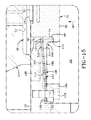
- FIG. 5 schematically shows a sectional view of the area labeled FIG. 5 in FIG. 2 .
- FIG. 6 schematically shows a sectional view of the area labeled FIG. 5 in FIG. 2 with a second implementation sealing member.
- FIG. 7 schematically shows a substrate processing chamber including a first sealing member and a second sealing member in a substrate loading position.
- FIG. 8 schematically shows a substrate processing chamber with a susceptor, a first sealing member, and a second sealing member in a processing position.
- FIG. 9 schematically shows a perspective view of a third implementation second sealing member.
- FIG. 10 schematically shows a sectional view of the area labeled FIG. 10 in FIG. 8 .
- FIG. 11 schematically shows a perspective view of fourth implementation second sealing member.
- FIG. 12 schematically shows a sectional view of the area labeled FIG. 10 in FIG. 8 with a fourth implementation second sealing member with the first and second sealing members disengaged.
- FIG. 13 schematically shows a sectional view taken generally about line 13 - 13 in FIG. 12 .
- FIG. 14 schematically shows a sectional view taken generally about line 14 - 14 in FIG. 13 .
- FIG. 15 schematically shows a sectional view of the area labeled FIG. 10 in FIG. 8 with a fourth implementation second sealing member with the first and second sealing members engaged.
- present aspects and implementations may be described in terms of functional block components and various processing steps. Such functional blocks may be realized by any number of hardware or software components configured to perform the specified functions and achieve the various results. For example, the present aspects may employ various sensors, detectors, flow control devices, heaters, and the like, which may carry out a variety of functions. In addition, the present aspects and implementations may be practiced in conjunction with any number of processing methods, and the apparatus and systems described may employ any number of processing methods, and the apparatus and systems described are merely examples of applications of the invention.
- FIGS. 1 and 2 illustrate views of a reaction chamber 20 in a loading/unloading position and a processing position, respectively.
- Reaction chamber 20 may include an upper region 22 and a lower region 24 , which may be separated by an interface plate 26 .
- a susceptor 28 includes a substrate mounting surface 30 and is connected to a vertically movable elevator 32 for displacing the susceptor between the substrate loading position and the substrate processing position.
- a substrate 34 may be positioned on substrate mounting surface 30 and may be located in a processing region 36 when positioned susceptor 28 is moved upwards in the direction of arrows 38 as shown in FIG. 2 with a showerhead 40 defining an upper surface of the processing region.
- a first sealing member 42 may be positioned on and removable from susceptor 28 , while a second sealing member 44 may be positioned between upper region 22 and lower region 24 .
- the second sealing member 44 may be positioned to rest at least partially on interface plate 26 or may connected to the interface plate or any other suitable portion of reaction chamber 20 without departing from the spirit and scope of the present disclosure.
- Susceptor 28 is shown with the first sealing member 42 and the second sealing member 44 attached and detached, respectively.
- Susceptor 28 includes an outer surface 46 and a ledge 48 extending outward of the outer surface 46 .
- Ledge 48 may be positioned generally near a lower surface 50 of the susceptor and is arranged to receive first sealing member 42 thereon.
- First sealing member 42 includes a lower portion 52 and an upper portion 54 , with the lower portion being positioned generally radially inward of the upper portion 54 in one implementation, although any suitable arrangements may be utilized.
- Lower portion 52 may include a bottom surface 56 arranged to rest on ledge 48 of the susceptor 28 when the first sealing member is being used to separate the upper region 22 and the lower region 24 .
- Upper portion 54 may include an upper surface 58 which assists with sealing by forming a portion of a tortuous path as will be discussed below in greater detail. Further, lower portion 52 may include an inner surface 60 and an outer surface 62 , while upper portion 54 may include an inner surface 64 and an outer surface 66 . Accordingly, upper portion 54 functions as a protrusion by extending upward from lower portion 52 as part of the first sealing member 42 .
- Second sealing member 44 may include an outer mounting ring 68 having a bottom surface 70 , with the outer mounting ring 68 partially defining a channel 72 .
- Bottom surface 70 is generally in contact with interface plate 26 when the second sealing member 44 is being used to provide separation between the upper region 22 and the lower region 24 .
- Outer ring 68 may also include a plurality of notches 74 which can be used to insure constant and consistent alignment with the other components in the reaction chamber.
- the second sealing member 44 may also include an outer protrusion 76 and an inner protrusion 78 generally extending downward.
- the outer protrusion 76 may include an outer surface 80 and an inner surface 82
- inner protrusion 78 may include an outer surface 84 and an inner surface 86 .
- outer surface 80 of outer protrusion 76 further defines channel 72 in second sealing member 44 , while outer surface 84 of inner protrusion 78 and inner surface 82 of outer protrusion 76 at least partially define a channel 88 for receiving upper portion 54 of the first sealing member 42 when the susceptor 28 travels upwards into the processing position.
- inner protrusion 78 and outer protrusion 76 may extend downward beyond bottom surface 70 since the bottom surface is positioned on an interface plate within the reaction chamber.
- the inner protrusion 78 may extend downwards a shorter distance than outer protrusion 76 .
- FIG. 5 illustrates an enlarged sectional view of the first sealing member 42 nested within a portion of second sealing member 44 when susceptor 28 is moved upwards into a processing position.
- upper portion 54 of first sealing member 42 is shown positioned within channel 88 formed at least partially between outer protrusion 76 , inner protrusion 78 , and a wall 90 .
- a gas path indicated by arrows 92 is generally less susceptible to transmitting gases from within the upper region 22 to the lower region 24 due to the tortuous path created by the first and second sealing members.
- the gas must travel through the tortuous path defined by a gap 94 formed between inner surfaces 60 and 64 of first sealing member 42 and an outer surface 46 of susceptor 28 , through channel 88 with upper portion 54 positioned therein, and finally into the lower region 24 .
- the width and lengths of the tortuous path may be optimized to permit a variable amount of communication between the upper and lower regions, or no communication between the upper and lower regions depending on the processing requirements.
- Both the first sealing member 42 and the second sealing member 44 may be composed of quartz, rutile, yttria, zirconia, Inconel, titanium, beryllium-copper, or any other suitable material.
- the first and second sealing members may increase or decrease in size depending on the temperature within reaction chamber 20 .
- first sealing member 42 is composed of quartz
- the first sealing member 42 tends to expand or grow when the temperature within the reaction chamber increases and particularly when the temperature increases near 400 degrees C.
- gap 94 may be decreased and the first sealing member 42 provides a self-centering function on the susceptor 28 .
- FIG. 6 another aspect of the first sealing member 42 and the second sealing member 44 are shown in section with the first sealing member 42 formed integral with susceptor 28 .
- a middle protrusion 96 is included in second sealing member 44 in addition to protrusions 98 , 100 , and 102 extending upward from susceptor 28 .
- ledge 48 of the first aspect has been replaced with three protrusions 98 , 100 , and 102 which are nested within channels 88 formed between each of the various protrusions extending downward from the second sealing member 44 .
- gas path 92 requires following a tortuous path through a plurality of channels 88 having protrusions 98 , 100 , and 102 therein to further restrict the gas flow path. Accordingly, even less gas flow communication is obtained between upper region 22 and lower region 24 when additional protrusions are included in the tortuous path.
- any number of protrusions may be utilized in the first and second sealing members depending on the restrictions of gas flow required by the tool or process. Further, the distances between the protrusions and open spaces there between may be optimized as may be necessary.
- the protrusions in the first sealing member 42 may be formed as part of a separate removable piece or may be formed integral with the susceptor, while the protrusions of the second sealing member 44 may be formed as a separate removable piece or may be formed integral to the reaction chamber 20 or an interface plate as may be appropriate.
- a first sealing member 104 is removably positionable on ledge 48 of susceptor 28
- a second sealing member 106 is generally positioned within lower region 24 and removably attached to interface plate 26 .
- second sealing member 106 may be removably secured to the interface plate 26 with a mounting plate 108 and a plurality of bolts 110 .
- the second sealing member 106 may be secured with the mounting plate at an outer perimeter 112 of a spring sealing member 114 in either lower region 24 or upper region 22 .
- the spring sealing member 114 may also include an inner perimeter 116 which may be deflected by first sealing member 104 when the susceptor 28 is moved in the direction associated with arrows 38 until a processing position is reached.
- spring sealing members 114 are shown with notches 118 on the outer perimeter 112 of the spring sealing member.
- 24 notches are included and a bolt is used to secure the spring sealing member to the mounting plate 108 at each of the notches and between the interface plate 26 and the mounting plate 108 .
- a plurality of slits 120 may be included around the inner perimeter 116 of the spring sealing member 114 to provide a minimal and controlled transfer rate between the upper and lower regions of the reaction chamber.
- the slits 120 may be radially aligned along the inner perimeter 116 and may include approximately 100 slits, or any other suitable number. It will be appreciated by a person of skill in the art that any suitable number of notches or slits may be utilized so long as the spring sealing member is properly secured and the gas flow rate between the upper region and the lower region is controlled.
- FIGS. 7, 8 and 10 illustrate views of spring sealing member 114 in an unbiased position ( FIG. 7 ) and a biased or deflected position ( FIGS. 8 and 10 ).
- spring sealing member 114 is resiliently bent upwards by a top surface 122 of the first sealing member 104 .
- top surface 122 is positioned on a flat portion of shelf 124 separated from ledge 48 by spacing portion 126 .
- spring sealing member 114 is bent upwards by contact at top surface 122 and thereby limits communication between the upper region and the lower region.
- the area between a flow control ring 128 , spring sealing member 114 , susceptor 28 , and gap 94 may collect some portion of a processing or purge gas, but this may ultimately be dissipated by vacuum measures, purging, or the disconnection between the first and second sealing members when the substrate is unloaded.
- FIGS. 11-15 two spring sealing members 114 are positioned one on top of the other as particularly shown in FIG. 12 .
- two spring sealing members 114 are positioned between mounting plate 108 and interface plate 26 , with bolts 110 maintaining the relationship between the components.
- FIGS. 13 and 14 illustrate the arrangement of the two spring sealing members 114 with slits 120 in each sealing member being aligned offset from one another such that slits 120 on an upper spring sealing member are positioned between slits 120 in the lower spring sealing member. In this arrangement, gas flow in the under region is prevented from flowing into the lower region when susceptor 28 is in a processing position as discussed with respect to FIGS. 7-10 , with the exception of slits 120 .
- the orientation of two spring sealing members 114 as seen in FIG. 14 may permit gas flow from the upper region through the upper spring sealing member at slits 120 and then through slits 120 in the lower spring sealing member.
- a tortuous path is again formed whereby a limited and controlled amount of gas flow may communicate between the upper region and the lower region as the process may require.
- the dual spring sealing member arrangement functions similar to a single spring sealing member as discussed above and only limits and/or prevents gas flow between the upper and lower regions when susceptor 28 and first sealing member 104 are moved upwards in the direction associated with arrow 38 and the susceptor is in a processing position.
- any number of slits 120 may be utilized depending on the desired communication between the upper and lower regions without departing from the spirit and scope of the present disclosure.
- any gas flow communication has been passing from the upper region 22 to the lower region 24 in a controlled and/or limited fashion. Nevertheless, it is within the spirit and scope of this disclosure to provide gas flow from the lower region to the upper region.
- a purge, an inert, or other gas flow within the lower region may be provided at a pressure which is greater than the gas flow pressure in the upper region.
- the higher pressure in the lower region would then permit gas flow from the lower region to communicate into the upper region through the various tortuous paths described and defined above.
- This arrangement may be useful to decrease purge times by limiting resonance within pockets and gaps in the upper region or reduce particle build-up in the lower region.
- the various sealing members gas flow communication may be selectively tuned to control the amount and direction of the gas flow between the upper and lower regions.
- the first sealing member 42 or 104 is positioned on susceptor 28 and may particularly be positioned on a ledge 48 if applicable.
- the second sealing member 44 or 106 is then positioned generally between the upper and lower regions, or in contact with an interface plate 26 , either above in the case of second sealing member 44 or below in the case of second sealing member 106 .
- the susceptor 28 is lowered to the substrate loading position where a substrate is positioned on lift pins.
- the susceptor is moved upwards in the direction associated with arrows 38 until the first sealing member forms a tortuous path with the second sealing member.
- the first and second sealing members contact one another when the susceptor is in a processing position, while in other implementations a small gap remains between the first and second sealing members, but is generally incorporated into the tortuous path.
- gas flow between the upper and lower regions is controlled and/or minimized when the susceptor is in a processing position. After the process is completed, the susceptor is lowered into the lower region and regular communication between the upper and lower regions may again be established until another substrate is loaded on the susceptor and the susceptor is moved into the processing position once again.
- the terms “comprises”, “comprising”, or any variation thereof, are intended to reference a non-exclusive inclusion, such that a process, method, article, composition or apparatus that comprises a list of elements does not include only those elements recited, but may also include other elements not expressly listed or inherent to such process, method, article, composition or apparatus.
- Other combinations and/or modifications of the above-described structures, arrangements, applications, proportions, elements, materials or components used in the practice of the present invention, in addition to those not specifically recited, may be varied or otherwise particularly adapted to specific environments, manufacturing specifications, design parameters or other operating requirements without departing from the general principles of the same.
Abstract
Description
Claims (23)
Priority Applications (1)
| Application Number | Priority Date | Filing Date | Title |
|---|---|---|---|
| US14/634,342 US9340874B2 (en) | 2011-11-23 | 2015-02-27 | Chamber sealing member |
Applications Claiming Priority (3)
| Application Number | Priority Date | Filing Date | Title |
|---|---|---|---|
| US201161563232P | 2011-11-23 | 2011-11-23 | |
| US13/677,151 US9005539B2 (en) | 2011-11-23 | 2012-11-14 | Chamber sealing member |
| US14/634,342 US9340874B2 (en) | 2011-11-23 | 2015-02-27 | Chamber sealing member |
Related Parent Applications (1)
| Application Number | Title | Priority Date | Filing Date |
|---|---|---|---|
| US13/677,151 Continuation US9005539B2 (en) | 2011-11-23 | 2012-11-14 | Chamber sealing member |
Publications (2)
| Publication Number | Publication Date |
|---|---|
| US20150167159A1 US20150167159A1 (en) | 2015-06-18 |
| US9340874B2 true US9340874B2 (en) | 2016-05-17 |
Family
ID=47501408
Family Applications (2)
| Application Number | Title | Priority Date | Filing Date |
|---|---|---|---|
| US13/677,151 Active 2033-03-17 US9005539B2 (en) | 2011-11-23 | 2012-11-14 | Chamber sealing member |
| US14/634,342 Active US9340874B2 (en) | 2011-11-23 | 2015-02-27 | Chamber sealing member |
Family Applications Before (1)
| Application Number | Title | Priority Date | Filing Date |
|---|---|---|---|
| US13/677,151 Active 2033-03-17 US9005539B2 (en) | 2011-11-23 | 2012-11-14 | Chamber sealing member |
Country Status (6)
| Country | Link |
|---|---|
| US (2) | US9005539B2 (en) |
| KR (2) | KR101860924B1 (en) |
| CN (1) | CN104081512B (en) |
| DE (1) | DE112012004880T5 (en) |
| TW (1) | TWI575106B (en) |
| WO (1) | WO2013078065A1 (en) |
Cited By (10)
| Publication number | Priority date | Publication date | Assignee | Title |
|---|---|---|---|---|
| USD795315S1 (en) * | 2014-12-12 | 2017-08-22 | Ebara Corporation | Dresser disk |
| US10998209B2 (en) | 2019-05-31 | 2021-05-04 | Applied Materials, Inc. | Substrate processing platforms including multiple processing chambers |
| US11276585B2 (en) | 2018-01-30 | 2022-03-15 | Samsung Electronics Co., Ltd. | Asymmetrical sealing and gas flow control device |
| US11447866B2 (en) * | 2020-06-17 | 2022-09-20 | Applied Materials, Inc. | High temperature chemical vapor deposition lid |
| US11600507B2 (en) | 2020-09-09 | 2023-03-07 | Applied Materials, Inc. | Pedestal assembly for a substrate processing chamber |
| US11610799B2 (en) | 2020-09-18 | 2023-03-21 | Applied Materials, Inc. | Electrostatic chuck having a heating and chucking capabilities |
| US11631571B2 (en) | 2019-08-12 | 2023-04-18 | Kurt J. Lesker Company | Ultra high purity conditions for atomic scale processing |
| US11674227B2 (en) | 2021-02-03 | 2023-06-13 | Applied Materials, Inc. | Symmetric pump down mini-volume with laminar flow cavity gas injection for high and low pressure |
| US11749542B2 (en) | 2020-07-27 | 2023-09-05 | Applied Materials, Inc. | Apparatus, system, and method for non-contact temperature monitoring of substrate supports |
| US11817331B2 (en) | 2020-07-27 | 2023-11-14 | Applied Materials, Inc. | Substrate holder replacement with protective disk during pasting process |
Families Citing this family (344)
| Publication number | Priority date | Publication date | Assignee | Title |
|---|---|---|---|---|
| US8986456B2 (en) * | 2006-10-10 | 2015-03-24 | Asm America, Inc. | Precursor delivery system |
| US10378106B2 (en) | 2008-11-14 | 2019-08-13 | Asm Ip Holding B.V. | Method of forming insulation film by modified PEALD |
| US9394608B2 (en) | 2009-04-06 | 2016-07-19 | Asm America, Inc. | Semiconductor processing reactor and components thereof |
| US8883270B2 (en) * | 2009-08-14 | 2014-11-11 | Asm America, Inc. | Systems and methods for thin-film deposition of metal oxides using excited nitrogen—oxygen species |
| US8877655B2 (en) | 2010-05-07 | 2014-11-04 | Asm America, Inc. | Systems and methods for thin-film deposition of metal oxides using excited nitrogen-oxygen species |
| US8802201B2 (en) | 2009-08-14 | 2014-08-12 | Asm America, Inc. | Systems and methods for thin-film deposition of metal oxides using excited nitrogen-oxygen species |
| US9312155B2 (en) | 2011-06-06 | 2016-04-12 | Asm Japan K.K. | High-throughput semiconductor-processing apparatus equipped with multiple dual-chamber modules |
| US9793148B2 (en) | 2011-06-22 | 2017-10-17 | Asm Japan K.K. | Method for positioning wafers in multiple wafer transport |
| US10364496B2 (en) | 2011-06-27 | 2019-07-30 | Asm Ip Holding B.V. | Dual section module having shared and unshared mass flow controllers |
| US10854498B2 (en) | 2011-07-15 | 2020-12-01 | Asm Ip Holding B.V. | Wafer-supporting device and method for producing same |
| US20130023129A1 (en) | 2011-07-20 | 2013-01-24 | Asm America, Inc. | Pressure transmitter for a semiconductor processing environment |
| US9096931B2 (en) | 2011-10-27 | 2015-08-04 | Asm America, Inc | Deposition valve assembly and method of heating the same |
| US9341296B2 (en) | 2011-10-27 | 2016-05-17 | Asm America, Inc. | Heater jacket for a fluid line |
| US9017481B1 (en) | 2011-10-28 | 2015-04-28 | Asm America, Inc. | Process feed management for semiconductor substrate processing |
| US9167625B2 (en) | 2011-11-23 | 2015-10-20 | Asm Ip Holding B.V. | Radiation shielding for a substrate holder |
| US9005539B2 (en) | 2011-11-23 | 2015-04-14 | Asm Ip Holding B.V. | Chamber sealing member |
| US9202727B2 (en) | 2012-03-02 | 2015-12-01 | ASM IP Holding | Susceptor heater shim |
| US8946830B2 (en) | 2012-04-04 | 2015-02-03 | Asm Ip Holdings B.V. | Metal oxide protective layer for a semiconductor device |
| US9029253B2 (en) | 2012-05-02 | 2015-05-12 | Asm Ip Holding B.V. | Phase-stabilized thin films, structures and devices including the thin films, and methods of forming same |
| US8728832B2 (en) | 2012-05-07 | 2014-05-20 | Asm Ip Holdings B.V. | Semiconductor device dielectric interface layer |
| US8933375B2 (en) | 2012-06-27 | 2015-01-13 | Asm Ip Holding B.V. | Susceptor heater and method of heating a substrate |
| US9558931B2 (en) | 2012-07-27 | 2017-01-31 | Asm Ip Holding B.V. | System and method for gas-phase sulfur passivation of a semiconductor surface |
| US9117866B2 (en) | 2012-07-31 | 2015-08-25 | Asm Ip Holding B.V. | Apparatus and method for calculating a wafer position in a processing chamber under process conditions |
| US9659799B2 (en) | 2012-08-28 | 2017-05-23 | Asm Ip Holding B.V. | Systems and methods for dynamic semiconductor process scheduling |
| US9169975B2 (en) | 2012-08-28 | 2015-10-27 | Asm Ip Holding B.V. | Systems and methods for mass flow controller verification |
| US9021985B2 (en) | 2012-09-12 | 2015-05-05 | Asm Ip Holdings B.V. | Process gas management for an inductively-coupled plasma deposition reactor |
| US9324811B2 (en) | 2012-09-26 | 2016-04-26 | Asm Ip Holding B.V. | Structures and devices including a tensile-stressed silicon arsenic layer and methods of forming same |
| US10714315B2 (en) | 2012-10-12 | 2020-07-14 | Asm Ip Holdings B.V. | Semiconductor reaction chamber showerhead |
| US9640416B2 (en) | 2012-12-26 | 2017-05-02 | Asm Ip Holding B.V. | Single-and dual-chamber module-attachable wafer-handling chamber |
| US8894870B2 (en) | 2013-02-01 | 2014-11-25 | Asm Ip Holding B.V. | Multi-step method and apparatus for etching compounds containing a metal |
| US9589770B2 (en) | 2013-03-08 | 2017-03-07 | Asm Ip Holding B.V. | Method and systems for in-situ formation of intermediate reactive species |
| US9484191B2 (en) | 2013-03-08 | 2016-11-01 | Asm Ip Holding B.V. | Pulsed remote plasma method and system |
| US8993054B2 (en) | 2013-07-12 | 2015-03-31 | Asm Ip Holding B.V. | Method and system to reduce outgassing in a reaction chamber |
| US9018111B2 (en) | 2013-07-22 | 2015-04-28 | Asm Ip Holding B.V. | Semiconductor reaction chamber with plasma capabilities |
| US9396934B2 (en) | 2013-08-14 | 2016-07-19 | Asm Ip Holding B.V. | Methods of forming films including germanium tin and structures and devices including the films |
| US9793115B2 (en) | 2013-08-14 | 2017-10-17 | Asm Ip Holding B.V. | Structures and devices including germanium-tin films and methods of forming same |
| US9240412B2 (en) | 2013-09-27 | 2016-01-19 | Asm Ip Holding B.V. | Semiconductor structure and device and methods of forming same using selective epitaxial process |
| US9556516B2 (en) | 2013-10-09 | 2017-01-31 | ASM IP Holding B.V | Method for forming Ti-containing film by PEALD using TDMAT or TDEAT |
| US9605343B2 (en) | 2013-11-13 | 2017-03-28 | Asm Ip Holding B.V. | Method for forming conformal carbon films, structures conformal carbon film, and system of forming same |
| US10179947B2 (en) | 2013-11-26 | 2019-01-15 | Asm Ip Holding B.V. | Method for forming conformal nitrided, oxidized, or carbonized dielectric film by atomic layer deposition |
| US10683571B2 (en) | 2014-02-25 | 2020-06-16 | Asm Ip Holding B.V. | Gas supply manifold and method of supplying gases to chamber using same |
| US10167557B2 (en) | 2014-03-18 | 2019-01-01 | Asm Ip Holding B.V. | Gas distribution system, reactor including the system, and methods of using the same |
| US9447498B2 (en) | 2014-03-18 | 2016-09-20 | Asm Ip Holding B.V. | Method for performing uniform processing in gas system-sharing multiple reaction chambers |
| US11015245B2 (en) | 2014-03-19 | 2021-05-25 | Asm Ip Holding B.V. | Gas-phase reactor and system having exhaust plenum and components thereof |
| US9404587B2 (en) | 2014-04-24 | 2016-08-02 | ASM IP Holding B.V | Lockout tagout for semiconductor vacuum valve |
| US10858737B2 (en) | 2014-07-28 | 2020-12-08 | Asm Ip Holding B.V. | Showerhead assembly and components thereof |
| US9543180B2 (en) | 2014-08-01 | 2017-01-10 | Asm Ip Holding B.V. | Apparatus and method for transporting wafers between wafer carrier and process tool under vacuum |
| US9890456B2 (en) | 2014-08-21 | 2018-02-13 | Asm Ip Holding B.V. | Method and system for in situ formation of gas-phase compounds |
| US10941490B2 (en) | 2014-10-07 | 2021-03-09 | Asm Ip Holding B.V. | Multiple temperature range susceptor, assembly, reactor and system including the susceptor, and methods of using the same |
| US9657845B2 (en) | 2014-10-07 | 2017-05-23 | Asm Ip Holding B.V. | Variable conductance gas distribution apparatus and method |
| KR102300403B1 (en) | 2014-11-19 | 2021-09-09 | 에이에스엠 아이피 홀딩 비.브이. | Method of depositing thin film |
| KR102263121B1 (en) | 2014-12-22 | 2021-06-09 | 에이에스엠 아이피 홀딩 비.브이. | Semiconductor device and manufacuring method thereof |
| US9478415B2 (en) | 2015-02-13 | 2016-10-25 | Asm Ip Holding B.V. | Method for forming film having low resistance and shallow junction depth |
| US10529542B2 (en) | 2015-03-11 | 2020-01-07 | Asm Ip Holdings B.V. | Cross-flow reactor and method |
| US10276355B2 (en) | 2015-03-12 | 2019-04-30 | Asm Ip Holding B.V. | Multi-zone reactor, system including the reactor, and method of using the same |
| US10458018B2 (en) | 2015-06-26 | 2019-10-29 | Asm Ip Holding B.V. | Structures including metal carbide material, devices including the structures, and methods of forming same |
| US10600673B2 (en) | 2015-07-07 | 2020-03-24 | Asm Ip Holding B.V. | Magnetic susceptor to baseplate seal |
| US10043661B2 (en) | 2015-07-13 | 2018-08-07 | Asm Ip Holding B.V. | Method for protecting layer by forming hydrocarbon-based extremely thin film |
| US9899291B2 (en) | 2015-07-13 | 2018-02-20 | Asm Ip Holding B.V. | Method for protecting layer by forming hydrocarbon-based extremely thin film |
| US10083836B2 (en) | 2015-07-24 | 2018-09-25 | Asm Ip Holding B.V. | Formation of boron-doped titanium metal films with high work function |
| US10087525B2 (en) | 2015-08-04 | 2018-10-02 | Asm Ip Holding B.V. | Variable gap hard stop design |
| US9647114B2 (en) | 2015-08-14 | 2017-05-09 | Asm Ip Holding B.V. | Methods of forming highly p-type doped germanium tin films and structures and devices including the films |
| US9711345B2 (en) | 2015-08-25 | 2017-07-18 | Asm Ip Holding B.V. | Method for forming aluminum nitride-based film by PEALD |
| JP5951095B1 (en) * | 2015-09-08 | 2016-07-13 | 株式会社日立国際電気 | Substrate processing apparatus, semiconductor device manufacturing method, and program |
| US9960072B2 (en) | 2015-09-29 | 2018-05-01 | Asm Ip Holding B.V. | Variable adjustment for precise matching of multiple chamber cavity housings |
| US9909214B2 (en) | 2015-10-15 | 2018-03-06 | Asm Ip Holding B.V. | Method for depositing dielectric film in trenches by PEALD |
| US10211308B2 (en) | 2015-10-21 | 2019-02-19 | Asm Ip Holding B.V. | NbMC layers |
| US10358721B2 (en) * | 2015-10-22 | 2019-07-23 | Asm Ip Holding B.V. | Semiconductor manufacturing system including deposition apparatus |
| US10322384B2 (en) | 2015-11-09 | 2019-06-18 | Asm Ip Holding B.V. | Counter flow mixer for process chamber |
| US9455138B1 (en) | 2015-11-10 | 2016-09-27 | Asm Ip Holding B.V. | Method for forming dielectric film in trenches by PEALD using H-containing gas |
| US9905420B2 (en) | 2015-12-01 | 2018-02-27 | Asm Ip Holding B.V. | Methods of forming silicon germanium tin films and structures and devices including the films |
| US9607837B1 (en) | 2015-12-21 | 2017-03-28 | Asm Ip Holding B.V. | Method for forming silicon oxide cap layer for solid state diffusion process |
| US9627221B1 (en) | 2015-12-28 | 2017-04-18 | Asm Ip Holding B.V. | Continuous process incorporating atomic layer etching |
| US9735024B2 (en) | 2015-12-28 | 2017-08-15 | Asm Ip Holding B.V. | Method of atomic layer etching using functional group-containing fluorocarbon |
| US11139308B2 (en) | 2015-12-29 | 2021-10-05 | Asm Ip Holding B.V. | Atomic layer deposition of III-V compounds to form V-NAND devices |
| US9754779B1 (en) | 2016-02-19 | 2017-09-05 | Asm Ip Holding B.V. | Method for forming silicon nitride film selectively on sidewalls or flat surfaces of trenches |
| US10468251B2 (en) | 2016-02-19 | 2019-11-05 | Asm Ip Holding B.V. | Method for forming spacers using silicon nitride film for spacer-defined multiple patterning |
| US10529554B2 (en) | 2016-02-19 | 2020-01-07 | Asm Ip Holding B.V. | Method for forming silicon nitride film selectively on sidewalls or flat surfaces of trenches |
| US10501866B2 (en) | 2016-03-09 | 2019-12-10 | Asm Ip Holding B.V. | Gas distribution apparatus for improved film uniformity in an epitaxial system |
| US10343920B2 (en) | 2016-03-18 | 2019-07-09 | Asm Ip Holding B.V. | Aligned carbon nanotubes |
| US9892913B2 (en) | 2016-03-24 | 2018-02-13 | Asm Ip Holding B.V. | Radial and thickness control via biased multi-port injection settings |
| US10865475B2 (en) | 2016-04-21 | 2020-12-15 | Asm Ip Holding B.V. | Deposition of metal borides and silicides |
| US10087522B2 (en) | 2016-04-21 | 2018-10-02 | Asm Ip Holding B.V. | Deposition of metal borides |
| US10190213B2 (en) | 2016-04-21 | 2019-01-29 | Asm Ip Holding B.V. | Deposition of metal borides |
| US10032628B2 (en) | 2016-05-02 | 2018-07-24 | Asm Ip Holding B.V. | Source/drain performance through conformal solid state doping |
| US10367080B2 (en) | 2016-05-02 | 2019-07-30 | Asm Ip Holding B.V. | Method of forming a germanium oxynitride film |
| KR102592471B1 (en) | 2016-05-17 | 2023-10-20 | 에이에스엠 아이피 홀딩 비.브이. | Method of forming metal interconnection and method of fabricating semiconductor device using the same |
| US11453943B2 (en) | 2016-05-25 | 2022-09-27 | Asm Ip Holding B.V. | Method for forming carbon-containing silicon/metal oxide or nitride film by ALD using silicon precursor and hydrocarbon precursor |
| US10388509B2 (en) | 2016-06-28 | 2019-08-20 | Asm Ip Holding B.V. | Formation of epitaxial layers via dislocation filtering |
| US10612137B2 (en) | 2016-07-08 | 2020-04-07 | Asm Ip Holdings B.V. | Organic reactants for atomic layer deposition |
| US9859151B1 (en) | 2016-07-08 | 2018-01-02 | Asm Ip Holding B.V. | Selective film deposition method to form air gaps |
| US9793135B1 (en) | 2016-07-14 | 2017-10-17 | ASM IP Holding B.V | Method of cyclic dry etching using etchant film |
| US10714385B2 (en) | 2016-07-19 | 2020-07-14 | Asm Ip Holding B.V. | Selective deposition of tungsten |
| US10381226B2 (en) | 2016-07-27 | 2019-08-13 | Asm Ip Holding B.V. | Method of processing substrate |
| US10395919B2 (en) | 2016-07-28 | 2019-08-27 | Asm Ip Holding B.V. | Method and apparatus for filling a gap |
| US9812320B1 (en) | 2016-07-28 | 2017-11-07 | Asm Ip Holding B.V. | Method and apparatus for filling a gap |
| KR102532607B1 (en) | 2016-07-28 | 2023-05-15 | 에이에스엠 아이피 홀딩 비.브이. | Substrate processing apparatus and method of operating the same |
| US10177025B2 (en) | 2016-07-28 | 2019-01-08 | Asm Ip Holding B.V. | Method and apparatus for filling a gap |
| US9887082B1 (en) | 2016-07-28 | 2018-02-06 | Asm Ip Holding B.V. | Method and apparatus for filling a gap |
| US10090316B2 (en) | 2016-09-01 | 2018-10-02 | Asm Ip Holding B.V. | 3D stacked multilayer semiconductor memory using doped select transistor channel |
| US10410943B2 (en) | 2016-10-13 | 2019-09-10 | Asm Ip Holding B.V. | Method for passivating a surface of a semiconductor and related systems |
| US10643826B2 (en) | 2016-10-26 | 2020-05-05 | Asm Ip Holdings B.V. | Methods for thermally calibrating reaction chambers |
| US11532757B2 (en) | 2016-10-27 | 2022-12-20 | Asm Ip Holding B.V. | Deposition of charge trapping layers |
| US10643904B2 (en) | 2016-11-01 | 2020-05-05 | Asm Ip Holdings B.V. | Methods for forming a semiconductor device and related semiconductor device structures |
| US10714350B2 (en) | 2016-11-01 | 2020-07-14 | ASM IP Holdings, B.V. | Methods for forming a transition metal niobium nitride film on a substrate by atomic layer deposition and related semiconductor device structures |
| US10229833B2 (en) | 2016-11-01 | 2019-03-12 | Asm Ip Holding B.V. | Methods for forming a transition metal nitride film on a substrate by atomic layer deposition and related semiconductor device structures |
| US10435790B2 (en) | 2016-11-01 | 2019-10-08 | Asm Ip Holding B.V. | Method of subatmospheric plasma-enhanced ALD using capacitively coupled electrodes with narrow gap |
| US10134757B2 (en) | 2016-11-07 | 2018-11-20 | Asm Ip Holding B.V. | Method of processing a substrate and a device manufactured by using the method |
| KR102546317B1 (en) | 2016-11-15 | 2023-06-21 | 에이에스엠 아이피 홀딩 비.브이. | Gas supply unit and substrate processing apparatus including the same |
| US10340135B2 (en) | 2016-11-28 | 2019-07-02 | Asm Ip Holding B.V. | Method of topologically restricted plasma-enhanced cyclic deposition of silicon or metal nitride |
| KR20180068582A (en) | 2016-12-14 | 2018-06-22 | 에이에스엠 아이피 홀딩 비.브이. | Substrate processing apparatus |
| US11581186B2 (en) | 2016-12-15 | 2023-02-14 | Asm Ip Holding B.V. | Sequential infiltration synthesis apparatus |
| US11447861B2 (en) | 2016-12-15 | 2022-09-20 | Asm Ip Holding B.V. | Sequential infiltration synthesis apparatus and a method of forming a patterned structure |
| US9916980B1 (en) | 2016-12-15 | 2018-03-13 | Asm Ip Holding B.V. | Method of forming a structure on a substrate |
| KR20180070971A (en) * | 2016-12-19 | 2018-06-27 | 에이에스엠 아이피 홀딩 비.브이. | Substrate processing apparatus |
| US10269558B2 (en) | 2016-12-22 | 2019-04-23 | Asm Ip Holding B.V. | Method of forming a structure on a substrate |
| US10867788B2 (en) | 2016-12-28 | 2020-12-15 | Asm Ip Holding B.V. | Method of forming a structure on a substrate |
| US11390950B2 (en) | 2017-01-10 | 2022-07-19 | Asm Ip Holding B.V. | Reactor system and method to reduce residue buildup during a film deposition process |
| EP3559307B1 (en) * | 2017-02-08 | 2022-08-03 | Picosun Oy | Deposition or cleaning apparatus with movable structure and method of operation |
| US10655221B2 (en) | 2017-02-09 | 2020-05-19 | Asm Ip Holding B.V. | Method for depositing oxide film by thermal ALD and PEALD |
| US10468261B2 (en) | 2017-02-15 | 2019-11-05 | Asm Ip Holding B.V. | Methods for forming a metallic film on a substrate by cyclical deposition and related semiconductor device structures |
| US10283353B2 (en) | 2017-03-29 | 2019-05-07 | Asm Ip Holding B.V. | Method of reforming insulating film deposited on substrate with recess pattern |
| US10529563B2 (en) | 2017-03-29 | 2020-01-07 | Asm Ip Holdings B.V. | Method for forming doped metal oxide films on a substrate by cyclical deposition and related semiconductor device structures |
| US10103040B1 (en) | 2017-03-31 | 2018-10-16 | Asm Ip Holding B.V. | Apparatus and method for manufacturing a semiconductor device |
| USD830981S1 (en) | 2017-04-07 | 2018-10-16 | Asm Ip Holding B.V. | Susceptor for semiconductor substrate processing apparatus |
| KR102457289B1 (en) | 2017-04-25 | 2022-10-21 | 에이에스엠 아이피 홀딩 비.브이. | Method for depositing a thin film and manufacturing a semiconductor device |
| US10770286B2 (en) | 2017-05-08 | 2020-09-08 | Asm Ip Holdings B.V. | Methods for selectively forming a silicon nitride film on a substrate and related semiconductor device structures |
| US10892156B2 (en) | 2017-05-08 | 2021-01-12 | Asm Ip Holding B.V. | Methods for forming a silicon nitride film on a substrate and related semiconductor device structures |
| US10446393B2 (en) | 2017-05-08 | 2019-10-15 | Asm Ip Holding B.V. | Methods for forming silicon-containing epitaxial layers and related semiconductor device structures |
| US10504742B2 (en) | 2017-05-31 | 2019-12-10 | Asm Ip Holding B.V. | Method of atomic layer etching using hydrogen plasma |
| US10886123B2 (en) | 2017-06-02 | 2021-01-05 | Asm Ip Holding B.V. | Methods for forming low temperature semiconductor layers and related semiconductor device structures |
| US11306395B2 (en) | 2017-06-28 | 2022-04-19 | Asm Ip Holding B.V. | Methods for depositing a transition metal nitride film on a substrate by atomic layer deposition and related deposition apparatus |
| US10685834B2 (en) | 2017-07-05 | 2020-06-16 | Asm Ip Holdings B.V. | Methods for forming a silicon germanium tin layer and related semiconductor device structures |
| KR20190009245A (en) | 2017-07-18 | 2019-01-28 | 에이에스엠 아이피 홀딩 비.브이. | Methods for forming a semiconductor device structure and related semiconductor device structures |
| US11018002B2 (en) | 2017-07-19 | 2021-05-25 | Asm Ip Holding B.V. | Method for selectively depositing a Group IV semiconductor and related semiconductor device structures |
| US11374112B2 (en) | 2017-07-19 | 2022-06-28 | Asm Ip Holding B.V. | Method for depositing a group IV semiconductor and related semiconductor device structures |
| US10541333B2 (en) | 2017-07-19 | 2020-01-21 | Asm Ip Holding B.V. | Method for depositing a group IV semiconductor and related semiconductor device structures |
| US10312055B2 (en) | 2017-07-26 | 2019-06-04 | Asm Ip Holding B.V. | Method of depositing film by PEALD using negative bias |
| US10590535B2 (en) | 2017-07-26 | 2020-03-17 | Asm Ip Holdings B.V. | Chemical treatment, deposition and/or infiltration apparatus and method for using the same |
| US10605530B2 (en) | 2017-07-26 | 2020-03-31 | Asm Ip Holding B.V. | Assembly of a liner and a flange for a vertical furnace as well as the liner and the vertical furnace |
| US10692741B2 (en) | 2017-08-08 | 2020-06-23 | Asm Ip Holdings B.V. | Radiation shield |
| US10770336B2 (en) | 2017-08-08 | 2020-09-08 | Asm Ip Holding B.V. | Substrate lift mechanism and reactor including same |
| US11769682B2 (en) | 2017-08-09 | 2023-09-26 | Asm Ip Holding B.V. | Storage apparatus for storing cassettes for substrates and processing apparatus equipped therewith |
| US11139191B2 (en) | 2017-08-09 | 2021-10-05 | Asm Ip Holding B.V. | Storage apparatus for storing cassettes for substrates and processing apparatus equipped therewith |
| US10249524B2 (en) | 2017-08-09 | 2019-04-02 | Asm Ip Holding B.V. | Cassette holder assembly for a substrate cassette and holding member for use in such assembly |
| US10236177B1 (en) | 2017-08-22 | 2019-03-19 | ASM IP Holding B.V.. | Methods for depositing a doped germanium tin semiconductor and related semiconductor device structures |
| USD900036S1 (en) | 2017-08-24 | 2020-10-27 | Asm Ip Holding B.V. | Heater electrical connector and adapter |
| US11830730B2 (en) | 2017-08-29 | 2023-11-28 | Asm Ip Holding B.V. | Layer forming method and apparatus |
| US11295980B2 (en) | 2017-08-30 | 2022-04-05 | Asm Ip Holding B.V. | Methods for depositing a molybdenum metal film over a dielectric surface of a substrate by a cyclical deposition process and related semiconductor device structures |
| US11056344B2 (en) | 2017-08-30 | 2021-07-06 | Asm Ip Holding B.V. | Layer forming method |
| KR102491945B1 (en) | 2017-08-30 | 2023-01-26 | 에이에스엠 아이피 홀딩 비.브이. | Substrate processing apparatus |
| US10607895B2 (en) | 2017-09-18 | 2020-03-31 | Asm Ip Holdings B.V. | Method for forming a semiconductor device structure comprising a gate fill metal |
| KR102630301B1 (en) | 2017-09-21 | 2024-01-29 | 에이에스엠 아이피 홀딩 비.브이. | Method of sequential infiltration synthesis treatment of infiltrateable material and structures and devices formed using same |
| US10844484B2 (en) | 2017-09-22 | 2020-11-24 | Asm Ip Holding B.V. | Apparatus for dispensing a vapor phase reactant to a reaction chamber and related methods |
| US10658205B2 (en) | 2017-09-28 | 2020-05-19 | Asm Ip Holdings B.V. | Chemical dispensing apparatus and methods for dispensing a chemical to a reaction chamber |
| US10403504B2 (en) | 2017-10-05 | 2019-09-03 | Asm Ip Holding B.V. | Method for selectively depositing a metallic film on a substrate |
| US10319588B2 (en) | 2017-10-10 | 2019-06-11 | Asm Ip Holding B.V. | Method for depositing a metal chalcogenide on a substrate by cyclical deposition |
| US10923344B2 (en) | 2017-10-30 | 2021-02-16 | Asm Ip Holding B.V. | Methods for forming a semiconductor structure and related semiconductor structures |
| US10872804B2 (en) * | 2017-11-03 | 2020-12-22 | Asm Ip Holding B.V. | Apparatus and methods for isolating a reaction chamber from a loading chamber resulting in reduced contamination |
| US10872803B2 (en) * | 2017-11-03 | 2020-12-22 | Asm Ip Holding B.V. | Apparatus and methods for isolating a reaction chamber from a loading chamber resulting in reduced contamination |
| US10910262B2 (en) | 2017-11-16 | 2021-02-02 | Asm Ip Holding B.V. | Method of selectively depositing a capping layer structure on a semiconductor device structure |
| KR102443047B1 (en) | 2017-11-16 | 2022-09-14 | 에이에스엠 아이피 홀딩 비.브이. | Method of processing a substrate and a device manufactured by the same |
| US11022879B2 (en) | 2017-11-24 | 2021-06-01 | Asm Ip Holding B.V. | Method of forming an enhanced unexposed photoresist layer |
| CN111316417B (en) | 2017-11-27 | 2023-12-22 | 阿斯莫Ip控股公司 | Storage device for storing wafer cassettes for use with batch ovens |
| JP7206265B2 (en) | 2017-11-27 | 2023-01-17 | エーエスエム アイピー ホールディング ビー.ブイ. | Equipment with a clean mini-environment |
| US10290508B1 (en) | 2017-12-05 | 2019-05-14 | Asm Ip Holding B.V. | Method for forming vertical spacers for spacer-defined patterning |
| US10872771B2 (en) | 2018-01-16 | 2020-12-22 | Asm Ip Holding B. V. | Method for depositing a material film on a substrate within a reaction chamber by a cyclical deposition process and related device structures |
| CN111630203A (en) | 2018-01-19 | 2020-09-04 | Asm Ip私人控股有限公司 | Method for depositing gap filling layer by plasma auxiliary deposition |
| TW202325889A (en) | 2018-01-19 | 2023-07-01 | 荷蘭商Asm 智慧財產控股公司 | Deposition method |
| USD903477S1 (en) | 2018-01-24 | 2020-12-01 | Asm Ip Holdings B.V. | Metal clamp |
| US11018047B2 (en) | 2018-01-25 | 2021-05-25 | Asm Ip Holding B.V. | Hybrid lift pin |
| US10535516B2 (en) | 2018-02-01 | 2020-01-14 | Asm Ip Holdings B.V. | Method for depositing a semiconductor structure on a surface of a substrate and related semiconductor structures |
| USD880437S1 (en) | 2018-02-01 | 2020-04-07 | Asm Ip Holding B.V. | Gas supply plate for semiconductor manufacturing apparatus |
| US11081345B2 (en) | 2018-02-06 | 2021-08-03 | Asm Ip Holding B.V. | Method of post-deposition treatment for silicon oxide film |
| US10896820B2 (en) | 2018-02-14 | 2021-01-19 | Asm Ip Holding B.V. | Method for depositing a ruthenium-containing film on a substrate by a cyclical deposition process |
| WO2019158960A1 (en) | 2018-02-14 | 2019-08-22 | Asm Ip Holding B.V. | A method for depositing a ruthenium-containing film on a substrate by a cyclical deposition process |
| US10731249B2 (en) | 2018-02-15 | 2020-08-04 | Asm Ip Holding B.V. | Method of forming a transition metal containing film on a substrate by a cyclical deposition process, a method for supplying a transition metal halide compound to a reaction chamber, and related vapor deposition apparatus |
| US10658181B2 (en) | 2018-02-20 | 2020-05-19 | Asm Ip Holding B.V. | Method of spacer-defined direct patterning in semiconductor fabrication |
| KR102636427B1 (en) | 2018-02-20 | 2024-02-13 | 에이에스엠 아이피 홀딩 비.브이. | Substrate processing method and apparatus |
| US10975470B2 (en) | 2018-02-23 | 2021-04-13 | Asm Ip Holding B.V. | Apparatus for detecting or monitoring for a chemical precursor in a high temperature environment |
| US11473195B2 (en) * | 2018-03-01 | 2022-10-18 | Asm Ip Holding B.V. | Semiconductor processing apparatus and a method for processing a substrate |
| US11629406B2 (en) | 2018-03-09 | 2023-04-18 | Asm Ip Holding B.V. | Semiconductor processing apparatus comprising one or more pyrometers for measuring a temperature of a substrate during transfer of the substrate |
| US11114283B2 (en) | 2018-03-16 | 2021-09-07 | Asm Ip Holding B.V. | Reactor, system including the reactor, and methods of manufacturing and using same |
| KR102646467B1 (en) | 2018-03-27 | 2024-03-11 | 에이에스엠 아이피 홀딩 비.브이. | Method of forming an electrode on a substrate and a semiconductor device structure including an electrode |
| US11088002B2 (en) | 2018-03-29 | 2021-08-10 | Asm Ip Holding B.V. | Substrate rack and a substrate processing system and method |
| US11230766B2 (en) | 2018-03-29 | 2022-01-25 | Asm Ip Holding B.V. | Substrate processing apparatus and method |
| US10510536B2 (en) | 2018-03-29 | 2019-12-17 | Asm Ip Holding B.V. | Method of depositing a co-doped polysilicon film on a surface of a substrate within a reaction chamber |
| KR102501472B1 (en) | 2018-03-30 | 2023-02-20 | 에이에스엠 아이피 홀딩 비.브이. | Substrate processing method |
| KR20190128558A (en) | 2018-05-08 | 2019-11-18 | 에이에스엠 아이피 홀딩 비.브이. | Methods for depositing an oxide film on a substrate by a cyclical deposition process and related device structures |
| TW202349473A (en) | 2018-05-11 | 2023-12-16 | 荷蘭商Asm Ip私人控股有限公司 | Methods for forming a doped metal carbide film on a substrate and related semiconductor device structures |
| KR102596988B1 (en) | 2018-05-28 | 2023-10-31 | 에이에스엠 아이피 홀딩 비.브이. | Method of processing a substrate and a device manufactured by the same |
| TW202013553A (en) | 2018-06-04 | 2020-04-01 | 荷蘭商Asm 智慧財產控股公司 | Wafer handling chamber with moisture reduction |
| US11718913B2 (en) | 2018-06-04 | 2023-08-08 | Asm Ip Holding B.V. | Gas distribution system and reactor system including same |
| US11286562B2 (en) | 2018-06-08 | 2022-03-29 | Asm Ip Holding B.V. | Gas-phase chemical reactor and method of using same |
| KR102568797B1 (en) | 2018-06-21 | 2023-08-21 | 에이에스엠 아이피 홀딩 비.브이. | Substrate processing system |
| US10797133B2 (en) | 2018-06-21 | 2020-10-06 | Asm Ip Holding B.V. | Method for depositing a phosphorus doped silicon arsenide film and related semiconductor device structures |
| WO2020003000A1 (en) | 2018-06-27 | 2020-01-02 | Asm Ip Holding B.V. | Cyclic deposition methods for forming metal-containing material and films and structures including the metal-containing material |
| CN112292478A (en) | 2018-06-27 | 2021-01-29 | Asm Ip私人控股有限公司 | Cyclic deposition methods for forming metal-containing materials and films and structures containing metal-containing materials |
| KR20200002519A (en) | 2018-06-29 | 2020-01-08 | 에이에스엠 아이피 홀딩 비.브이. | Method for depositing a thin film and manufacturing a semiconductor device |
| US10612136B2 (en) | 2018-06-29 | 2020-04-07 | ASM IP Holding, B.V. | Temperature-controlled flange and reactor system including same |
| US10755922B2 (en) | 2018-07-03 | 2020-08-25 | Asm Ip Holding B.V. | Method for depositing silicon-free carbon-containing film as gap-fill layer by pulse plasma-assisted deposition |
| US10388513B1 (en) | 2018-07-03 | 2019-08-20 | Asm Ip Holding B.V. | Method for depositing silicon-free carbon-containing film as gap-fill layer by pulse plasma-assisted deposition |
| US10767789B2 (en) | 2018-07-16 | 2020-09-08 | Asm Ip Holding B.V. | Diaphragm valves, valve components, and methods for forming valve components |
| US10483099B1 (en) | 2018-07-26 | 2019-11-19 | Asm Ip Holding B.V. | Method for forming thermally stable organosilicon polymer film |
| US11053591B2 (en) | 2018-08-06 | 2021-07-06 | Asm Ip Holding B.V. | Multi-port gas injection system and reactor system including same |
| US10883175B2 (en) | 2018-08-09 | 2021-01-05 | Asm Ip Holding B.V. | Vertical furnace for processing substrates and a liner for use therein |
| JP7225599B2 (en) * | 2018-08-10 | 2023-02-21 | 東京エレクトロン株式会社 | Deposition equipment |
| US10829852B2 (en) | 2018-08-16 | 2020-11-10 | Asm Ip Holding B.V. | Gas distribution device for a wafer processing apparatus |
| US11430674B2 (en) | 2018-08-22 | 2022-08-30 | Asm Ip Holding B.V. | Sensor array, apparatus for dispensing a vapor phase reactant to a reaction chamber and related methods |
| KR20200030162A (en) | 2018-09-11 | 2020-03-20 | 에이에스엠 아이피 홀딩 비.브이. | Method for deposition of a thin film |
| US11024523B2 (en) | 2018-09-11 | 2021-06-01 | Asm Ip Holding B.V. | Substrate processing apparatus and method |
| US11049751B2 (en) | 2018-09-14 | 2021-06-29 | Asm Ip Holding B.V. | Cassette supply system to store and handle cassettes and processing apparatus equipped therewith |
| CN110970344A (en) | 2018-10-01 | 2020-04-07 | Asm Ip控股有限公司 | Substrate holding apparatus, system including the same, and method of using the same |
| US11232963B2 (en) | 2018-10-03 | 2022-01-25 | Asm Ip Holding B.V. | Substrate processing apparatus and method |
| KR102592699B1 (en) | 2018-10-08 | 2023-10-23 | 에이에스엠 아이피 홀딩 비.브이. | Substrate support unit and apparatuses for depositing thin film and processing the substrate including the same |
| US10847365B2 (en) | 2018-10-11 | 2020-11-24 | Asm Ip Holding B.V. | Method of forming conformal silicon carbide film by cyclic CVD |
| CN111058093B (en) * | 2018-10-16 | 2020-11-10 | 北京北方华创微电子装备有限公司 | Chamber sealing assembly and growth furnace |
| US10811256B2 (en) | 2018-10-16 | 2020-10-20 | Asm Ip Holding B.V. | Method for etching a carbon-containing feature |
| KR102605121B1 (en) | 2018-10-19 | 2023-11-23 | 에이에스엠 아이피 홀딩 비.브이. | Substrate processing apparatus and substrate processing method |
| KR102546322B1 (en) | 2018-10-19 | 2023-06-21 | 에이에스엠 아이피 홀딩 비.브이. | Substrate processing apparatus and substrate processing method |
| USD948463S1 (en) | 2018-10-24 | 2022-04-12 | Asm Ip Holding B.V. | Susceptor for semiconductor substrate supporting apparatus |
| US10381219B1 (en) | 2018-10-25 | 2019-08-13 | Asm Ip Holding B.V. | Methods for forming a silicon nitride film |
| US11087997B2 (en) | 2018-10-31 | 2021-08-10 | Asm Ip Holding B.V. | Substrate processing apparatus for processing substrates |
| KR20200051105A (en) | 2018-11-02 | 2020-05-13 | 에이에스엠 아이피 홀딩 비.브이. | Substrate support unit and substrate processing apparatus including the same |
| US11572620B2 (en) | 2018-11-06 | 2023-02-07 | Asm Ip Holding B.V. | Methods for selectively depositing an amorphous silicon film on a substrate |
| US11031242B2 (en) | 2018-11-07 | 2021-06-08 | Asm Ip Holding B.V. | Methods for depositing a boron doped silicon germanium film |
| US10847366B2 (en) | 2018-11-16 | 2020-11-24 | Asm Ip Holding B.V. | Methods for depositing a transition metal chalcogenide film on a substrate by a cyclical deposition process |
| US10818758B2 (en) | 2018-11-16 | 2020-10-27 | Asm Ip Holding B.V. | Methods for forming a metal silicate film on a substrate in a reaction chamber and related semiconductor device structures |
| US10559458B1 (en) | 2018-11-26 | 2020-02-11 | Asm Ip Holding B.V. | Method of forming oxynitride film |
| US11217444B2 (en) | 2018-11-30 | 2022-01-04 | Asm Ip Holding B.V. | Method for forming an ultraviolet radiation responsive metal oxide-containing film |
| KR102636428B1 (en) | 2018-12-04 | 2024-02-13 | 에이에스엠 아이피 홀딩 비.브이. | A method for cleaning a substrate processing apparatus |
| US11158513B2 (en) | 2018-12-13 | 2021-10-26 | Asm Ip Holding B.V. | Methods for forming a rhenium-containing film on a substrate by a cyclical deposition process and related semiconductor device structures |
| TW202037745A (en) | 2018-12-14 | 2020-10-16 | 荷蘭商Asm Ip私人控股有限公司 | Method of forming device structure, structure formed by the method and system for performing the method |
| TWI819180B (en) | 2019-01-17 | 2023-10-21 | 荷蘭商Asm 智慧財產控股公司 | Methods of forming a transition metal containing film on a substrate by a cyclical deposition process |
| KR20200091543A (en) | 2019-01-22 | 2020-07-31 | 에이에스엠 아이피 홀딩 비.브이. | Semiconductor processing device |
| CN111524788B (en) | 2019-02-01 | 2023-11-24 | Asm Ip私人控股有限公司 | Method for topologically selective film formation of silicon oxide |
| JP2020136678A (en) | 2019-02-20 | 2020-08-31 | エーエスエム・アイピー・ホールディング・ベー・フェー | Method for filing concave part formed inside front surface of base material, and device |
| US11482533B2 (en) | 2019-02-20 | 2022-10-25 | Asm Ip Holding B.V. | Apparatus and methods for plug fill deposition in 3-D NAND applications |
| TW202104632A (en) | 2019-02-20 | 2021-02-01 | 荷蘭商Asm Ip私人控股有限公司 | Cyclical deposition method and apparatus for filling a recess formed within a substrate surface |
| KR102626263B1 (en) | 2019-02-20 | 2024-01-16 | 에이에스엠 아이피 홀딩 비.브이. | Cyclical deposition method including treatment step and apparatus for same |
| TW202100794A (en) | 2019-02-22 | 2021-01-01 | 荷蘭商Asm Ip私人控股有限公司 | Substrate processing apparatus and method for processing substrate |
| KR20200108243A (en) | 2019-03-08 | 2020-09-17 | 에이에스엠 아이피 홀딩 비.브이. | Structure Including SiOC Layer and Method of Forming Same |
| KR20200108242A (en) | 2019-03-08 | 2020-09-17 | 에이에스엠 아이피 홀딩 비.브이. | Method for Selective Deposition of Silicon Nitride Layer and Structure Including Selectively-Deposited Silicon Nitride Layer |
| US11742198B2 (en) | 2019-03-08 | 2023-08-29 | Asm Ip Holding B.V. | Structure including SiOCN layer and method of forming same |
| JP2020167398A (en) | 2019-03-28 | 2020-10-08 | エーエスエム・アイピー・ホールディング・ベー・フェー | Door opener and substrate processing apparatus provided therewith |
| KR20200116855A (en) | 2019-04-01 | 2020-10-13 | 에이에스엠 아이피 홀딩 비.브이. | Method of manufacturing semiconductor device |
| KR20200123380A (en) | 2019-04-19 | 2020-10-29 | 에이에스엠 아이피 홀딩 비.브이. | Layer forming method and apparatus |
| KR20200125453A (en) | 2019-04-24 | 2020-11-04 | 에이에스엠 아이피 홀딩 비.브이. | Gas-phase reactor system and method of using same |
| KR20200130121A (en) | 2019-05-07 | 2020-11-18 | 에이에스엠 아이피 홀딩 비.브이. | Chemical source vessel with dip tube |
| KR20200130118A (en) | 2019-05-07 | 2020-11-18 | 에이에스엠 아이피 홀딩 비.브이. | Method for Reforming Amorphous Carbon Polymer Film |
| KR20200130652A (en) | 2019-05-10 | 2020-11-19 | 에이에스엠 아이피 홀딩 비.브이. | Method of depositing material onto a surface and structure formed according to the method |
| JP2020188255A (en) | 2019-05-16 | 2020-11-19 | エーエスエム アイピー ホールディング ビー.ブイ. | Wafer boat handling device, vertical batch furnace, and method |
| USD975665S1 (en) | 2019-05-17 | 2023-01-17 | Asm Ip Holding B.V. | Susceptor shaft |
| USD947913S1 (en) | 2019-05-17 | 2022-04-05 | Asm Ip Holding B.V. | Susceptor shaft |
| USD935572S1 (en) | 2019-05-24 | 2021-11-09 | Asm Ip Holding B.V. | Gas channel plate |
| USD922229S1 (en) | 2019-06-05 | 2021-06-15 | Asm Ip Holding B.V. | Device for controlling a temperature of a gas supply unit |
| KR20200141002A (en) | 2019-06-06 | 2020-12-17 | 에이에스엠 아이피 홀딩 비.브이. | Method of using a gas-phase reactor system including analyzing exhausted gas |
| KR20200143254A (en) | 2019-06-11 | 2020-12-23 | 에이에스엠 아이피 홀딩 비.브이. | Method of forming an electronic structure using an reforming gas, system for performing the method, and structure formed using the method |
| USD944946S1 (en) | 2019-06-14 | 2022-03-01 | Asm Ip Holding B.V. | Shower plate |
| USD931978S1 (en) | 2019-06-27 | 2021-09-28 | Asm Ip Holding B.V. | Showerhead vacuum transport |
| KR20210005515A (en) | 2019-07-03 | 2021-01-14 | 에이에스엠 아이피 홀딩 비.브이. | Temperature control assembly for substrate processing apparatus and method of using same |
| JP2021015791A (en) | 2019-07-09 | 2021-02-12 | エーエスエム アイピー ホールディング ビー.ブイ. | Plasma device and substrate processing method using coaxial waveguide |
| CN112216646A (en) | 2019-07-10 | 2021-01-12 | Asm Ip私人控股有限公司 | Substrate supporting assembly and substrate processing device comprising same |
| KR20210010307A (en) | 2019-07-16 | 2021-01-27 | 에이에스엠 아이피 홀딩 비.브이. | Substrate processing apparatus |
| KR20210010816A (en) | 2019-07-17 | 2021-01-28 | 에이에스엠 아이피 홀딩 비.브이. | Radical assist ignition plasma system and method |
| KR20210010820A (en) | 2019-07-17 | 2021-01-28 | 에이에스엠 아이피 홀딩 비.브이. | Methods of forming silicon germanium structures |
| US11643724B2 (en) | 2019-07-18 | 2023-05-09 | Asm Ip Holding B.V. | Method of forming structures using a neutral beam |
| TW202121506A (en) | 2019-07-19 | 2021-06-01 | 荷蘭商Asm Ip私人控股有限公司 | Method of forming topology-controlled amorphous carbon polymer film |
| CN112309843A (en) | 2019-07-29 | 2021-02-02 | Asm Ip私人控股有限公司 | Selective deposition method for achieving high dopant doping |
| CN112309900A (en) | 2019-07-30 | 2021-02-02 | Asm Ip私人控股有限公司 | Substrate processing apparatus |
| CN112309899A (en) | 2019-07-30 | 2021-02-02 | Asm Ip私人控股有限公司 | Substrate processing apparatus |
| US20210032750A1 (en) * | 2019-07-31 | 2021-02-04 | Taiwan Semiconductor Manufacturing Co., Ltd. | Deposition apparatus and method of forming metal oxide layer using the same |
| US11227782B2 (en) | 2019-07-31 | 2022-01-18 | Asm Ip Holding B.V. | Vertical batch furnace assembly |
| US11587815B2 (en) | 2019-07-31 | 2023-02-21 | Asm Ip Holding B.V. | Vertical batch furnace assembly |
| US11587814B2 (en) | 2019-07-31 | 2023-02-21 | Asm Ip Holding B.V. | Vertical batch furnace assembly |
| CN112323048B (en) | 2019-08-05 | 2024-02-09 | Asm Ip私人控股有限公司 | Liquid level sensor for chemical source container |
| USD965524S1 (en) | 2019-08-19 | 2022-10-04 | Asm Ip Holding B.V. | Susceptor support |
| USD965044S1 (en) | 2019-08-19 | 2022-09-27 | Asm Ip Holding B.V. | Susceptor shaft |
| JP2021031769A (en) | 2019-08-21 | 2021-03-01 | エーエスエム アイピー ホールディング ビー.ブイ. | Production apparatus of mixed gas of film deposition raw material and film deposition apparatus |
| KR20210024423A (en) | 2019-08-22 | 2021-03-05 | 에이에스엠 아이피 홀딩 비.브이. | Method for forming a structure with a hole |
| USD949319S1 (en) * | 2019-08-22 | 2022-04-19 | Asm Ip Holding B.V. | Exhaust duct |
| USD940837S1 (en) | 2019-08-22 | 2022-01-11 | Asm Ip Holding B.V. | Electrode |
| USD979506S1 (en) | 2019-08-22 | 2023-02-28 | Asm Ip Holding B.V. | Insulator |
| USD930782S1 (en) | 2019-08-22 | 2021-09-14 | Asm Ip Holding B.V. | Gas distributor |
| US11286558B2 (en) | 2019-08-23 | 2022-03-29 | Asm Ip Holding B.V. | Methods for depositing a molybdenum nitride film on a surface of a substrate by a cyclical deposition process and related semiconductor device structures including a molybdenum nitride film |
| KR20210024420A (en) | 2019-08-23 | 2021-03-05 | 에이에스엠 아이피 홀딩 비.브이. | Method for depositing silicon oxide film having improved quality by peald using bis(diethylamino)silane |
| KR20210029090A (en) | 2019-09-04 | 2021-03-15 | 에이에스엠 아이피 홀딩 비.브이. | Methods for selective deposition using a sacrificial capping layer |
| KR20210029663A (en) | 2019-09-05 | 2021-03-16 | 에이에스엠 아이피 홀딩 비.브이. | Substrate processing apparatus |
| US11562901B2 (en) | 2019-09-25 | 2023-01-24 | Asm Ip Holding B.V. | Substrate processing method |
| CN112593212B (en) | 2019-10-02 | 2023-12-22 | Asm Ip私人控股有限公司 | Method for forming topologically selective silicon oxide film by cyclic plasma enhanced deposition process |
| TW202129060A (en) | 2019-10-08 | 2021-08-01 | 荷蘭商Asm Ip控股公司 | Substrate processing device, and substrate processing method |
| TW202115273A (en) | 2019-10-10 | 2021-04-16 | 荷蘭商Asm Ip私人控股有限公司 | Method of forming a photoresist underlayer and structure including same |
| KR20210045930A (en) | 2019-10-16 | 2021-04-27 | 에이에스엠 아이피 홀딩 비.브이. | Method of Topology-Selective Film Formation of Silicon Oxide |
| US11637014B2 (en) | 2019-10-17 | 2023-04-25 | Asm Ip Holding B.V. | Methods for selective deposition of doped semiconductor material |
| KR20210047808A (en) | 2019-10-21 | 2021-04-30 | 에이에스엠 아이피 홀딩 비.브이. | Apparatus and methods for selectively etching films |
| US11646205B2 (en) | 2019-10-29 | 2023-05-09 | Asm Ip Holding B.V. | Methods of selectively forming n-type doped material on a surface, systems for selectively forming n-type doped material, and structures formed using same |
| KR20210054983A (en) | 2019-11-05 | 2021-05-14 | 에이에스엠 아이피 홀딩 비.브이. | Structures with doped semiconductor layers and methods and systems for forming same |
| US11501968B2 (en) | 2019-11-15 | 2022-11-15 | Asm Ip Holding B.V. | Method for providing a semiconductor device with silicon filled gaps |
| KR20210062561A (en) | 2019-11-20 | 2021-05-31 | 에이에스엠 아이피 홀딩 비.브이. | Method of depositing carbon-containing material on a surface of a substrate, structure formed using the method, and system for forming the structure |
| CN112951697A (en) | 2019-11-26 | 2021-06-11 | Asm Ip私人控股有限公司 | Substrate processing apparatus |
| KR20210065848A (en) | 2019-11-26 | 2021-06-04 | 에이에스엠 아이피 홀딩 비.브이. | Methods for selectivley forming a target film on a substrate comprising a first dielectric surface and a second metallic surface |
| CN112885693A (en) | 2019-11-29 | 2021-06-01 | Asm Ip私人控股有限公司 | Substrate processing apparatus |
| CN112885692A (en) | 2019-11-29 | 2021-06-01 | Asm Ip私人控股有限公司 | Substrate processing apparatus |
| JP2021090042A (en) | 2019-12-02 | 2021-06-10 | エーエスエム アイピー ホールディング ビー.ブイ. | Substrate processing apparatus and substrate processing method |
| KR20210070898A (en) | 2019-12-04 | 2021-06-15 | 에이에스엠 아이피 홀딩 비.브이. | Substrate processing apparatus |
| KR20210078405A (en) | 2019-12-17 | 2021-06-28 | 에이에스엠 아이피 홀딩 비.브이. | Method of forming vanadium nitride layer and structure including the vanadium nitride layer |
| US11527403B2 (en) | 2019-12-19 | 2022-12-13 | Asm Ip Holding B.V. | Methods for filling a gap feature on a substrate surface and related semiconductor structures |
| KR20210095050A (en) | 2020-01-20 | 2021-07-30 | 에이에스엠 아이피 홀딩 비.브이. | Method of forming thin film and method of modifying surface of thin film |
| TW202130846A (en) | 2020-02-03 | 2021-08-16 | 荷蘭商Asm Ip私人控股有限公司 | Method of forming structures including a vanadium or indium layer |
| TW202146882A (en) | 2020-02-04 | 2021-12-16 | 荷蘭商Asm Ip私人控股有限公司 | Method of verifying an article, apparatus for verifying an article, and system for verifying a reaction chamber |
| US11776846B2 (en) | 2020-02-07 | 2023-10-03 | Asm Ip Holding B.V. | Methods for depositing gap filling fluids and related systems and devices |
| TW202146715A (en) | 2020-02-17 | 2021-12-16 | 荷蘭商Asm Ip私人控股有限公司 | Method for growing phosphorous-doped silicon layer and system of the same |
| KR20210116240A (en) | 2020-03-11 | 2021-09-27 | 에이에스엠 아이피 홀딩 비.브이. | Substrate handling device with adjustable joints |
| US11876356B2 (en) | 2020-03-11 | 2024-01-16 | Asm Ip Holding B.V. | Lockout tagout assembly and system and method of using same |
| KR20210124042A (en) | 2020-04-02 | 2021-10-14 | 에이에스엠 아이피 홀딩 비.브이. | Thin film forming method |
| TW202146689A (en) | 2020-04-03 | 2021-12-16 | 荷蘭商Asm Ip控股公司 | Method for forming barrier layer and method for manufacturing semiconductor device |
| TW202145344A (en) | 2020-04-08 | 2021-12-01 | 荷蘭商Asm Ip私人控股有限公司 | Apparatus and methods for selectively etching silcon oxide films |
| US11821078B2 (en) | 2020-04-15 | 2023-11-21 | Asm Ip Holding B.V. | Method for forming precoat film and method for forming silicon-containing film |
| US11898243B2 (en) | 2020-04-24 | 2024-02-13 | Asm Ip Holding B.V. | Method of forming vanadium nitride-containing layer |
| KR20210132605A (en) | 2020-04-24 | 2021-11-04 | 에이에스엠 아이피 홀딩 비.브이. | Vertical batch furnace assembly comprising a cooling gas supply |
| KR20210132600A (en) | 2020-04-24 | 2021-11-04 | 에이에스엠 아이피 홀딩 비.브이. | Methods and systems for depositing a layer comprising vanadium, nitrogen, and a further element |
| KR20210134869A (en) | 2020-05-01 | 2021-11-11 | 에이에스엠 아이피 홀딩 비.브이. | Fast FOUP swapping with a FOUP handler |
| KR20210141379A (en) | 2020-05-13 | 2021-11-23 | 에이에스엠 아이피 홀딩 비.브이. | Laser alignment fixture for a reactor system |
| KR20210143653A (en) | 2020-05-19 | 2021-11-29 | 에이에스엠 아이피 홀딩 비.브이. | Substrate processing apparatus |
| KR20210145078A (en) | 2020-05-21 | 2021-12-01 | 에이에스엠 아이피 홀딩 비.브이. | Structures including multiple carbon layers and methods of forming and using same |
| TW202201602A (en) | 2020-05-29 | 2022-01-01 | 荷蘭商Asm Ip私人控股有限公司 | Substrate processing device |
| TW202218133A (en) | 2020-06-24 | 2022-05-01 | 荷蘭商Asm Ip私人控股有限公司 | Method for forming a layer provided with silicon |
| TW202217953A (en) | 2020-06-30 | 2022-05-01 | 荷蘭商Asm Ip私人控股有限公司 | Substrate processing method |
| KR20220010438A (en) | 2020-07-17 | 2022-01-25 | 에이에스엠 아이피 홀딩 비.브이. | Structures and methods for use in photolithography |
| TW202204662A (en) | 2020-07-20 | 2022-02-01 | 荷蘭商Asm Ip私人控股有限公司 | Method and system for depositing molybdenum layers |
| TW202212623A (en) | 2020-08-26 | 2022-04-01 | 荷蘭商Asm Ip私人控股有限公司 | Method of forming metal silicon oxide layer and metal silicon oxynitride layer, semiconductor structure, and system |
| USD990534S1 (en) | 2020-09-11 | 2023-06-27 | Asm Ip Holding B.V. | Weighted lift pin |
| USD1012873S1 (en) | 2020-09-24 | 2024-01-30 | Asm Ip Holding B.V. | Electrode for semiconductor processing apparatus |
| TW202229613A (en) | 2020-10-14 | 2022-08-01 | 荷蘭商Asm Ip私人控股有限公司 | Method of depositing material on stepped structure |
| TW202217037A (en) | 2020-10-22 | 2022-05-01 | 荷蘭商Asm Ip私人控股有限公司 | Method of depositing vanadium metal, structure, device and a deposition assembly |
| TW202223136A (en) | 2020-10-28 | 2022-06-16 | 荷蘭商Asm Ip私人控股有限公司 | Method for forming layer on substrate, and semiconductor processing system |
| TW202235675A (en) | 2020-11-30 | 2022-09-16 | 荷蘭商Asm Ip私人控股有限公司 | Injector, and substrate processing apparatus |
| US11946137B2 (en) | 2020-12-16 | 2024-04-02 | Asm Ip Holding B.V. | Runout and wobble measurement fixtures |
| TW202231903A (en) | 2020-12-22 | 2022-08-16 | 荷蘭商Asm Ip私人控股有限公司 | Transition metal deposition method, transition metal layer, and deposition assembly for depositing transition metal on substrate |
| USD980814S1 (en) | 2021-05-11 | 2023-03-14 | Asm Ip Holding B.V. | Gas distributor for substrate processing apparatus |
| USD980813S1 (en) | 2021-05-11 | 2023-03-14 | Asm Ip Holding B.V. | Gas flow control plate for substrate processing apparatus |
| USD981973S1 (en) | 2021-05-11 | 2023-03-28 | Asm Ip Holding B.V. | Reactor wall for substrate processing apparatus |
| WO2023027706A1 (en) * | 2021-08-25 | 2023-03-02 | Applied Materials, Inc. | Process gas containment using elastic objects mated with reactor frames |
| USD990441S1 (en) | 2021-09-07 | 2023-06-27 | Asm Ip Holding B.V. | Gas flow control plate |
Citations (385)
| Publication number | Priority date | Publication date | Assignee | Title |
|---|---|---|---|---|
| US2745640A (en) | 1953-09-24 | 1956-05-15 | American Viscose Corp | Heat exchanging apparatus |
| US2990045A (en) | 1959-09-18 | 1961-06-27 | Lipe Rollway Corp | Thermally responsive transmission for automobile fan |
| US3833492A (en) | 1971-09-22 | 1974-09-03 | Pollution Control Ind Inc | Method of producing ozone |
| US3854443A (en) | 1973-12-19 | 1974-12-17 | Intel Corp | Gas reactor for depositing thin films |
| US3862397A (en) | 1972-03-24 | 1975-01-21 | Applied Materials Tech | Cool wall radiantly heated reactor |
| US3887790A (en) | 1974-10-07 | 1975-06-03 | Vernon H Ferguson | Wrap-around electric resistance heater |
| US4058430A (en) | 1974-11-29 | 1977-11-15 | Tuomo Suntola | Method for producing compound thin films |
| US4176630A (en) | 1977-06-01 | 1979-12-04 | Dynair Limited | Automatic control valves |
| US4194536A (en) | 1976-12-09 | 1980-03-25 | Eaton Corporation | Composite tubing product |
| US4322592A (en) | 1980-08-22 | 1982-03-30 | Rca Corporation | Susceptor for heating semiconductor substrates |
| US4389973A (en) | 1980-03-18 | 1983-06-28 | Oy Lohja Ab | Apparatus for performing growth of compound thin films |
| US4393013A (en) | 1970-05-20 | 1983-07-12 | J. C. Schumacher Company | Vapor mass flow control system |
| US4436674A (en) | 1981-07-30 | 1984-03-13 | J.C. Schumacher Co. | Vapor mass flow control system |
| US4499354A (en) | 1982-10-06 | 1985-02-12 | General Instrument Corp. | Susceptor for radiant absorption heater system |
| US4512113A (en) | 1982-09-23 | 1985-04-23 | Budinger William D | Workpiece holder for polishing operation |
| US4570328A (en) | 1983-03-07 | 1986-02-18 | Motorola, Inc. | Method of producing titanium nitride MOS device gate electrode |
| USD288556S (en) | 1984-02-21 | 1987-03-03 | Pace, Incorporated | Ornamental design for a frame of circuit elements utilized to replace damaged elements on printed circuit boards |
| US4653541A (en) | 1985-06-26 | 1987-03-31 | Parker Hannifin Corporation | Dual wall safety tube |
| US4722298A (en) | 1986-05-19 | 1988-02-02 | Machine Technology, Inc. | Modular processing apparatus for processing semiconductor wafers |
| US4735259A (en) | 1984-02-21 | 1988-04-05 | Hewlett-Packard Company | Heated transfer line for capillary tubing |
| US4753192A (en) | 1987-01-08 | 1988-06-28 | Btu Engineering Corporation | Movable core fast cool-down furnace |
| US4789294A (en) | 1985-08-30 | 1988-12-06 | Canon Kabushiki Kaisha | Wafer handling apparatus and method |
| US4821674A (en) | 1987-03-31 | 1989-04-18 | Deboer Wiebe B | Rotatable substrate supporting mechanism with temperature sensing device for use in chemical vapor deposition equipment |
| US4827430A (en) | 1987-05-11 | 1989-05-02 | Baxter International Inc. | Flow measurement system |
| US4882199A (en) | 1986-08-15 | 1989-11-21 | Massachusetts Institute Of Technology | Method of forming a metal coating on a substrate |
| US4986215A (en) | 1988-09-01 | 1991-01-22 | Kyushu Electronic Metal Co., Ltd. | Susceptor for vapor-phase growth system |
| US4991614A (en) | 1987-06-25 | 1991-02-12 | Kvaerner Engineering A/S | Method and a plant for transport of hydrocarbons over a long distance from an offshore source of hydrocarbons |
| US5062386A (en) | 1987-07-27 | 1991-11-05 | Epitaxy Systems, Inc. | Induction heated pancake epitaxial reactor |
| US5074017A (en) | 1989-01-13 | 1991-12-24 | Toshiba Ceramics Co., Ltd. | Susceptor |
| US5119760A (en) | 1988-12-27 | 1992-06-09 | Symetrix Corporation | Methods and apparatus for material deposition |
| US5167716A (en) | 1990-09-28 | 1992-12-01 | Gasonics, Inc. | Method and apparatus for batch processing a semiconductor wafer |
| US5199603A (en) | 1991-11-26 | 1993-04-06 | Prescott Norman F | Delivery system for organometallic compounds |
| US5221556A (en) | 1987-06-24 | 1993-06-22 | Epsilon Technology, Inc. | Gas injectors for reaction chambers in CVD systems |
| US5243195A (en) | 1991-04-25 | 1993-09-07 | Nikon Corporation | Projection exposure apparatus having an off-axis alignment system and method of alignment therefor |
| US5242539A (en) | 1991-04-04 | 1993-09-07 | Hitachi, Ltd. | Plasma treatment method and apparatus |
| US5326427A (en) | 1992-09-11 | 1994-07-05 | Lsi Logic Corporation | Method of selectively etching titanium-containing materials on a semiconductor wafer using remote plasma generation |
| US5380367A (en) | 1992-12-04 | 1995-01-10 | Cselt - Centro Studi E Laboratori Telecomunicazioni S.P.A. | Vapour generator for chemical vapour deposition systems |
| US5422139A (en) | 1990-04-12 | 1995-06-06 | Balzers Aktiengesellschaft | Method for a reactive surface treatment of a workpiece and a treatment chamber for practicing such method |
| US5421893A (en) | 1993-02-26 | 1995-06-06 | Applied Materials, Inc. | Susceptor drive and wafer displacement mechanism |
| JPH07283149A (en) | 1994-04-04 | 1995-10-27 | Nissin Electric Co Ltd | Thin film vapor growth device |
| US5518549A (en) | 1995-04-18 | 1996-05-21 | Memc Electronic Materials, Inc. | Susceptor and baffle therefor |
| JPH08335558A (en) | 1995-06-08 | 1996-12-17 | Nissin Electric Co Ltd | Thin film vapor phase deposition apparatus |
| US5595606A (en) | 1995-04-20 | 1997-01-21 | Tokyo Electron Limited | Shower head and film forming apparatus using the same |
| US5632919A (en) | 1996-01-25 | 1997-05-27 | T.G.M., Inc. | Temperature controlled insulation system |
| US5681779A (en) | 1994-02-04 | 1997-10-28 | Lsi Logic Corporation | Method of doping metal layers for electromigration resistance |
| US5695567A (en) | 1996-02-26 | 1997-12-09 | Abb Research Ltd. | Susceptor for a device for epitaxially growing objects and such a device |
| US5730801A (en) | 1994-08-23 | 1998-03-24 | Applied Materials, Inc. | Compartnetalized substrate processing chamber |
| US5732744A (en) | 1996-03-08 | 1998-03-31 | Control Systems, Inc. | Method and apparatus for aligning and supporting semiconductor process gas delivery and regulation components |
| US5736314A (en) | 1995-11-16 | 1998-04-07 | Microfab Technologies, Inc. | Inline thermo-cycler |
| US5796074A (en) | 1995-11-28 | 1998-08-18 | Applied Materials, Inc. | Wafer heater assembly |
| US5836483A (en) | 1997-02-05 | 1998-11-17 | Aerotech Dental Systems, Inc. | Self-regulating fluid dispensing cap with safety pressure relief valve for dental/medical unit fluid bottles |
| US5837320A (en) | 1996-02-27 | 1998-11-17 | The University Of New Mexico | Chemical vapor deposition of metal sulfide films from metal thiocarboxylate complexes with monodenate or multidentate ligands |
| US5855680A (en) | 1994-11-28 | 1999-01-05 | Neste Oy | Apparatus for growing thin films |
| US5920798A (en) | 1996-05-28 | 1999-07-06 | Matsushita Battery Industrial Co., Ltd. | Method of preparing a semiconductor layer for an optical transforming device |
| US5979506A (en) | 1995-08-16 | 1999-11-09 | Aker Engineering As | Arrangement in a pipe bundle |
| US6013553A (en) | 1997-07-24 | 2000-01-11 | Texas Instruments Incorporated | Zirconium and/or hafnium oxynitride gate dielectric |
| US6015465A (en) | 1998-04-08 | 2000-01-18 | Applied Materials, Inc. | Temperature control system for semiconductor process chamber |
| US6035101A (en) | 1997-02-12 | 2000-03-07 | Applied Materials, Inc. | High temperature multi-layered alloy heater assembly and related methods |
| US6060691A (en) | 1997-04-21 | 2000-05-09 | Fujikin Incorporated | Device for heating fluid controller |
| US6074443A (en) | 1996-10-21 | 2000-06-13 | Applied Materials, Inc. | Method and apparatus for scheduling wafer processing within a multiple chamber semiconductor wafer processing tool having a multiple blade robot |
| US6083321A (en) | 1997-07-11 | 2000-07-04 | Applied Materials, Inc. | Fluid delivery system and method |
| US6086677A (en) | 1998-06-16 | 2000-07-11 | Applied Materials, Inc. | Dual gas faceplate for a showerhead in a semiconductor wafer processing system |
| US6122036A (en) | 1993-10-21 | 2000-09-19 | Nikon Corporation | Projection exposure apparatus and method |
| US6125789A (en) | 1998-01-30 | 2000-10-03 | Applied Materials, Inc. | Increasing the sensitivity of an in-situ particle monitor |
| US6129044A (en) | 1996-07-12 | 2000-10-10 | Applied Materials, Inc. | Apparatus for substrate processing with improved throughput and yield |
| US6148761A (en) | 1998-06-16 | 2000-11-21 | Applied Materials, Inc. | Dual channel gas distribution plate |
| US6160244A (en) | 1998-05-29 | 2000-12-12 | Ngk Insulators, Ltd. | Susceptors |
| US6161500A (en) | 1997-09-30 | 2000-12-19 | Tokyo Electron Limited | Apparatus and method for preventing the premature mixture of reactant gases in CVD and PECVD reactions |
| US6201999B1 (en) | 1997-06-09 | 2001-03-13 | Applied Materials, Inc. | Method and apparatus for automatically generating schedules for wafer processing within a multichamber semiconductor wafer processing tool |
| US6274878B1 (en) | 1997-07-23 | 2001-08-14 | Applied Materials, Inc. | Wafer out-of-pocket detection method |
| US20010017103A1 (en) | 1997-12-15 | 2001-08-30 | Tokyo Electron Limited | Method of coating film, coating unit, aging unit, solvent replacement unit, and apparatus for coating film |
| US6287965B1 (en) | 1997-07-28 | 2001-09-11 | Samsung Electronics Co, Ltd. | Method of forming metal layer using atomic layer deposition and semiconductor device having the metal layer as barrier metal layer or upper or lower electrode of capacitor |
| US6302964B1 (en) | 1998-06-16 | 2001-10-16 | Applied Materials, Inc. | One-piece dual gas faceplate for a showerhead in a semiconductor wafer processing system |
| US6312525B1 (en) | 1997-07-11 | 2001-11-06 | Applied Materials, Inc. | Modular architecture for semiconductor wafer fabrication equipment |
| US20010046765A1 (en) | 2000-05-05 | 2001-11-29 | Annalisa Cappellani | Method for producing a barrier layer in an electronic component and method for producing an electronic component with a barrier layer |
| US6326597B1 (en) | 1999-04-15 | 2001-12-04 | Applied Materials, Inc. | Temperature control system for process chamber |
| USD451893S1 (en) | 1998-10-15 | 2001-12-11 | Meto International Gmbh | Arrangement of aluminum foil coils forming an inductor of a resonant frequency identification element |
| JP2001342570A (en) | 2000-03-30 | 2001-12-14 | Hitachi Kokusai Electric Inc | Manufacturing method of semiconductor device and manufacturing apparatus of semiconductor |
| US20020001974A1 (en) | 2000-06-30 | 2002-01-03 | Lim Chan | Method for manufacturing zirconium oxide film for use in semiconductor device |
| US6342427B1 (en) | 1999-12-02 | 2002-01-29 | Electronics And Telecommunications Research Institute | Method for forming micro cavity |
| US20020011210A1 (en) | 2000-01-18 | 2002-01-31 | Kiyoshi Satoh | Semiconductor-processing device provided with a remote plasma source for self-cleaning |
| US6367410B1 (en) | 1996-12-16 | 2002-04-09 | Applied Materials, Inc. | Closed-loop dome thermal control apparatus for a semiconductor wafer processing system |
| US6383566B1 (en) | 1999-06-30 | 2002-05-07 | Saint-Gobain Vitrage | Process for depositing a tungsten-based and/or molybdenum-based layer on a rigid substrate, and substrate thus coated |
| US20020064592A1 (en) | 2000-11-29 | 2002-05-30 | Madhav Datta | Electroless method of seed layer depostion, repair, and fabrication of Cu interconnects |
| US6410459B2 (en) | 1999-09-02 | 2002-06-25 | Micron Technology, Inc. | Wafer planarization using a uniform layer of material and method and apparatus for forming uniform layer of material used in semiconductor processing |
| US6420279B1 (en) | 2001-06-28 | 2002-07-16 | Sharp Laboratories Of America, Inc. | Methods of using atomic layer deposition to deposit a high dielectric constant material on a substrate |
| US20020098627A1 (en) | 2000-11-24 | 2002-07-25 | Pomarede Christophe F. | Surface preparation prior to deposition |
| US20020108670A1 (en) | 2001-02-12 | 2002-08-15 | Baker John Eric | High purity chemical container with external level sensor and removable dip tube |
| US20020115252A1 (en) | 2000-10-10 | 2002-08-22 | Haukka Suvi P. | Dielectric interface films and methods therefor |
| US6454860B2 (en) | 1998-10-27 | 2002-09-24 | Applied Materials, Inc. | Deposition reactor having vaporizing, mixing and cleaning capabilities |
| US6478872B1 (en) | 1999-01-18 | 2002-11-12 | Samsung Electronics Co., Ltd. | Method of delivering gas into reaction chamber and shower head used to deliver gas |
| US6483989B1 (en) | 2000-11-21 | 2002-11-19 | Hitachi Kokusai Electric Inc. | Substrate processing apparatus and semiconductor device producing method |
| US6482331B2 (en) | 2001-04-18 | 2002-11-19 | Taiwan Semiconductor Manufacturing Co., Ltd. | Method for preventing contamination in a plasma process chamber |
| US20020172768A1 (en) | 2001-05-21 | 2002-11-21 | Nec Corporation | Method for vapor deposition of a metal compound film |
| US6511539B1 (en) | 1999-09-08 | 2003-01-28 | Asm America, Inc. | Apparatus and method for growth of a thin film |
| US20030019580A1 (en) | 2000-03-30 | 2003-01-30 | Strang Eric J. | Method of and apparatus for tunable gas injection in a plasma processing system |
| US20030025146A1 (en) | 2001-07-23 | 2003-02-06 | Pravin Narwankar | Processes for making a barrier between a dielectric and a conductor and products produced therefrom |
| US6521295B1 (en) | 2001-04-17 | 2003-02-18 | Pilkington North America, Inc. | Chemical vapor deposition of antimony-doped metal oxide and the coated article made thereby |
| US20030040158A1 (en) | 2001-08-21 | 2003-02-27 | Nec Corporation | Semiconductor device and method of fabricating the same |
| US20030042419A1 (en) | 1999-12-21 | 2003-03-06 | Hirohumi Katsumata | Method and apparatus for detecting a wafer's posture on a susceptor |
| US6534395B2 (en) | 2000-03-07 | 2003-03-18 | Asm Microchemistry Oy | Method of forming graded thin films using alternating pulses of vapor phase reactants |
| US20030066826A1 (en) | 2001-10-05 | 2003-04-10 | Samsung Electronics Co., Ltd. | Apparatus for processing a substrate including a heating apparatus |
| US20030075925A1 (en) | 2001-07-03 | 2003-04-24 | Sven Lindfors | Source chemical container assembly |
| US20030094133A1 (en) | 2001-11-21 | 2003-05-22 | Applied Materials, Inc. | Piezoelectric vaporizer |
| US6569239B2 (en) | 1998-07-29 | 2003-05-27 | Shin-Etsu Handotai Co., Ltd. | Silicon epitaxial wafer and production method therefor |
| US6579833B1 (en) | 1999-09-01 | 2003-06-17 | The Board Of Trustees Of The University Of Illinois | Process for converting a metal carbide to carbon by etching in halogens |
| US20030111963A1 (en) | 2001-12-14 | 2003-06-19 | Tolmachev Yuri Nikolaevich | Inductively coupled plasma system |
| US6590251B2 (en) | 1999-12-08 | 2003-07-08 | Samsung Electronics Co., Ltd. | Semiconductor devices having metal layers as barrier layers on upper or lower electrodes of capacitors |
| US6594550B1 (en) | 2002-03-29 | 2003-07-15 | Asm America, Inc. | Method and system for using a buffer to track robotic movement |
| US6598559B1 (en) | 2000-03-24 | 2003-07-29 | Applied Materials, Inc. | Temperature controlled chamber |
| US20030141820A1 (en) | 2002-01-30 | 2003-07-31 | Applied Materials, Inc. | Method and apparatus for substrate processing |
| US6627503B2 (en) | 2000-02-11 | 2003-09-30 | Sharp Laboratories Of America, Inc. | Method of forming a multilayer dielectric stack |
| US6633364B2 (en) | 2000-03-31 | 2003-10-14 | Nikon Corporation | Exposure apparatus, exposure method, and device manufacturing method |
| US6645304B2 (en) | 2000-10-23 | 2003-11-11 | Ngk Insulators, Ltd. | Susceptors for semiconductor-producing apparatuses |
| US6648974B1 (en) | 1999-02-12 | 2003-11-18 | Lpe Spa | Device and method for handling substrates by means of a self-leveling vacuum system in epitaxial induction |
| US20030228772A1 (en) | 2002-06-05 | 2003-12-11 | Cowans Kenneth W. | Lateral temperature equalizing system for large area surfaces during processing |
| US20030232138A1 (en) | 2002-06-17 | 2003-12-18 | Marko Tuominen | System for controlling the sublimation of reactants |
| US6673196B1 (en) | 1999-09-02 | 2004-01-06 | Tokyo Electron Limited | Plasma processing apparatus |
| JP2004014952A (en) | 2002-06-10 | 2004-01-15 | Tokyo Electron Ltd | Processing system and processing method |
| US20040013577A1 (en) | 2002-07-17 | 2004-01-22 | Seshadri Ganguli | Method and apparatus for providing gas to a processing chamber |
| US6682973B1 (en) | 2002-05-16 | 2004-01-27 | Advanced Micro Devices, Inc. | Formation of well-controlled thin SiO, SiN, SiON layer for multilayer high-K dielectric applications |
| US20040023516A1 (en) | 2001-10-02 | 2004-02-05 | Londergan Ana R. | Passivation method for improved uniformity and repeatability for atomic layer deposition and chemical vapor deposition |
| US20040036129A1 (en) | 2002-08-22 | 2004-02-26 | Micron Technology, Inc. | Atomic layer deposition of CMOS gates with variable work functions |
| US6709989B2 (en) | 2001-06-21 | 2004-03-23 | Motorola, Inc. | Method for fabricating a semiconductor structure including a metal oxide interface with silicon |
| US6710364B2 (en) | 1999-09-24 | 2004-03-23 | Texas Instruments Incorporated | Semiconductor wafer edge marking |
| JP2004091848A (en) | 2002-08-30 | 2004-03-25 | Tokyo Electron Ltd | Gaseous raw material supply system for thin film forming apparatus and thin film forming apparatus |
| US20040077182A1 (en) | 2002-10-22 | 2004-04-22 | Lim Jung-Wook | Method for forming introgen-containing oxide thin film using plasma enhanced atomic layer deposition |
| US6734090B2 (en) | 2002-02-20 | 2004-05-11 | International Business Machines Corporation | Method of making an edge seal for a semiconductor device |
| US20040106249A1 (en) | 2002-12-03 | 2004-06-03 | Hannu Huotari | Method to fabricate dual metal CMOS devices |
| US20040144980A1 (en) | 2003-01-27 | 2004-07-29 | Ahn Kie Y. | Atomic layer deposition of metal oxynitride layers as gate dielectrics and semiconductor device structures utilizing metal oxynitride layers |
| US20040169032A1 (en) | 2003-02-27 | 2004-09-02 | Dainippon Screen Mfg. Co., Ltd. | Heat treatment apparatus by means of light irradiation |
| US20040168627A1 (en) | 2003-02-27 | 2004-09-02 | Sharp Laboratories Of America, Inc. | Atomic layer deposition of oxide film |
| US20040198069A1 (en) | 2003-04-04 | 2004-10-07 | Applied Materials, Inc. | Method for hafnium nitride deposition |
| US20040200499A1 (en) | 2003-04-11 | 2004-10-14 | Applied Materials, Inc. | Backflush chamber clean |
| US20040219793A1 (en) | 2000-12-05 | 2004-11-04 | Shingo Hishiya | Method and apparatus for treating article to be treated |
| US20040221807A1 (en) | 2003-05-09 | 2004-11-11 | Mohith Verghese | Reactor surface passivation through chemical deactivation |
| US6821910B2 (en) | 2000-07-24 | 2004-11-23 | University Of Maryland, College Park | Spatially programmable microelectronics process equipment using segmented gas injection showerhead with exhaust gas recirculation |
| US6820570B2 (en) | 2001-08-15 | 2004-11-23 | Nobel Biocare Services Ag | Atomic layer deposition reactor |
| US6824665B2 (en) | 2000-10-25 | 2004-11-30 | Shipley Company, L.L.C. | Seed layer deposition |
| US20040266011A1 (en) | 2003-06-26 | 2004-12-30 | Samsung Electronics Co., Ltd. | In-situ analysis method for atomic layer deposition process |
| TWI226380B (en) | 1999-12-03 | 2005-01-11 | Asm Int | Method of growing oxide films |
| CN1563483A (en) | 2004-04-01 | 2005-01-12 | 南昌大学 | Bilayer inlet gas spray nozzle in use for metal-organic chemical vapor deposition device |
| US20050008799A1 (en) | 2003-07-08 | 2005-01-13 | Shizuo Tomiyasu | Solid organometallic compound-filled container and filling method thereof |
| US6847014B1 (en) | 2001-04-30 | 2005-01-25 | Lam Research Corporation | Method and apparatus for controlling the spatial temperature distribution across the surface of a workpiece support |
| US20050019026A1 (en) | 2003-07-23 | 2005-01-27 | Luping Wang | Delivery systems for efficient vaporization of precursor source material |
| US20050020071A1 (en) | 2001-07-31 | 2005-01-27 | Jun Sonobe | Method and apparatus for cleaning and method and apparatus for etching |
| US20050023624A1 (en) | 2002-06-05 | 2005-02-03 | Micron Technology, Inc. | Atomic layer-deposited HfAlO3 films for gate dielectrics |
| US6858524B2 (en) | 2002-12-03 | 2005-02-22 | Asm International, Nv | Method of depositing barrier layer for metal gates |
| US6858547B2 (en) | 2002-06-14 | 2005-02-22 | Applied Materials, Inc. | System and method for forming a gate dielectric |
| US6863019B2 (en) | 2000-06-13 | 2005-03-08 | Applied Materials, Inc. | Semiconductor device fabrication chamber cleaning method and apparatus with recirculation of cleaning gas |
| US20050054228A1 (en) | 2003-05-01 | 2005-03-10 | March David Martin | Mid-line connector and method for pipe-in-pipe electrical heating |
| JP2005507030A (en) | 2001-10-26 | 2005-03-10 | アプライド マテリアルズ インコーポレイテッド | Gas delivery device for atomic layer deposition |
| US20050066893A1 (en) | 2003-09-29 | 2005-03-31 | Soininen Pekka T. | Safe liquid source containers |
| US20050070123A1 (en) | 2003-08-27 | 2005-03-31 | Tomoyuki Hirano | Method for forming a thin film and method for fabricating a semiconductor device |
| US6874480B1 (en) | 2000-07-03 | 2005-04-05 | Combustion Dynamics Corp. | Flow meter |
| US6875677B1 (en) | 2003-09-30 | 2005-04-05 | Sharp Laboratories Of America, Inc. | Method to control the interfacial layer for deposition of high dielectric constant films |
| US20050072357A1 (en) | 2002-07-30 | 2005-04-07 | Shero Eric J. | Sublimation bed employing carrier gas guidance structures |
| US6884319B2 (en) | 2001-11-12 | 2005-04-26 | Jusung Engineering Co., Ltd. | Susceptor of apparatus for manufacturing semiconductor device |
| US6884066B2 (en) | 2002-09-10 | 2005-04-26 | Fsi International, Inc. | Thermal process station with heated lid |
| US20050100669A1 (en) | 2003-11-12 | 2005-05-12 | Veeco Instruments, Inc. | Method and apparatus for fabricating a conformal thin film on a substrate |
| US20050106893A1 (en) | 2003-08-04 | 2005-05-19 | Glen Wilk | Surface preparation prior to deposition on germanium |
| US20050110069A1 (en) | 2003-11-22 | 2005-05-26 | Hynix Semiconductor Inc. | Hafnium oxide and aluminium oxide alloyed dielectric layer and method for fabricating the same |
| US20050173003A1 (en) | 2002-07-19 | 2005-08-11 | Mykrolis Corporation | Liquid flow controller and precision dispense apparatus and system |
| US6930059B2 (en) | 2003-02-27 | 2005-08-16 | Sharp Laboratories Of America, Inc. | Method for depositing a nanolaminate film by atomic layer deposition |
| US20050187647A1 (en) | 2004-02-19 | 2005-08-25 | Kuo-Hua Wang | Intelligent full automation controlled flow for a semiconductor furnace tool |
| US6935269B2 (en) | 2000-05-02 | 2005-08-30 | Sem Technology Co., Ltd. | Apparatus for treating the surface with neutral particle beams |
| US20050212119A1 (en) | 2001-10-02 | 2005-09-29 | Shero Eric J | Incorporation of nitrogen into high k dielectric film |
| US20050214457A1 (en) | 2004-03-29 | 2005-09-29 | Applied Materials, Inc. | Deposition of low dielectric constant films by N2O addition |
| US20050214458A1 (en) | 2004-03-01 | 2005-09-29 | Meiere Scott H | Low zirconium hafnium halide compositions |
| US6955836B2 (en) | 2001-12-25 | 2005-10-18 | Anelva Corporation | Silicon oxide film formation method |
| US20050229972A1 (en) | 2001-03-05 | 2005-10-20 | George Hoshi | Fluid controller |
| US20050229848A1 (en) | 2004-04-15 | 2005-10-20 | Asm Japan K.K. | Thin-film deposition apparatus |
| US20050241176A1 (en) | 2003-10-29 | 2005-11-03 | Shero Eric J | Reaction system for growing a thin film |
| US20050260347A1 (en) | 2004-05-21 | 2005-11-24 | Narwankar Pravin K | Formation of a silicon oxynitride layer on a high-k dielectric material |
| US6972478B1 (en) | 2005-03-07 | 2005-12-06 | Advanced Micro Devices, Inc. | Integrated circuit and method for its manufacture |
| US20050271813A1 (en) | 2004-05-12 | 2005-12-08 | Shreyas Kher | Apparatuses and methods for atomic layer deposition of hafnium-containing high-k dielectric materials |
| US20050282101A1 (en) | 2004-06-21 | 2005-12-22 | Naoshi Adachi | Heat treatment jig for silicon semiconductor substrate |
| US20060013946A1 (en) | 2004-07-15 | 2006-01-19 | Park Hong-Bae | Methods of forming a thin film structure, and a gate structure and a capacitor including the thin film structure |
| US20060014384A1 (en) | 2002-06-05 | 2006-01-19 | Jong-Cheol Lee | Method of forming a layer and forming a capacitor of a semiconductor device having the same layer |
| US20060019033A1 (en) | 2004-05-21 | 2006-01-26 | Applied Materials, Inc. | Plasma treatment of hafnium-containing materials |
| US20060046518A1 (en) | 2004-08-31 | 2006-03-02 | Micron Technology, Inc. | Method of increasing deposition rate of silicon dioxide on a catalyst |
| US20060063346A1 (en) | 2004-06-10 | 2006-03-23 | Jong-Cheol Lee | Method of forming a layer and method of forming a capacitor of a semiconductor device having the same |
| US20060060930A1 (en) | 2004-09-17 | 2006-03-23 | Metz Matthew V | Atomic layer deposition of high dielectric constant gate dielectrics |
| US20060062910A1 (en) | 2004-03-01 | 2006-03-23 | Meiere Scott H | Low zirconium, hafnium-containing compositions, processes for the preparation thereof and methods of use thereof |
| US20060068125A1 (en) | 2004-09-30 | 2006-03-30 | Gouri Radhakrishnan | Method for producing carbon surface films by plasma exposure of a carbide compound |
| US7045430B2 (en) | 2002-05-02 | 2006-05-16 | Micron Technology Inc. | Atomic layer-deposited LaAlO3 films for gate dielectrics |
| US20060110934A1 (en) | 2004-11-08 | 2006-05-25 | Yusuke Fukuchi | Method and apparatus for forming insulating film |
| WO2006056091A1 (en) | 2004-11-24 | 2006-06-01 | Oc Oerlikon Balzers Ag | Vacuum processing chamber for very large area substrates |
| US20060113675A1 (en) | 2004-12-01 | 2006-06-01 | Chung-Liang Chang | Barrier material and process for Cu interconnect |
| US20060128168A1 (en) | 2004-12-13 | 2006-06-15 | Micron Technology, Inc. | Atomic layer deposited lanthanum hafnium oxide dielectrics |
| US7071051B1 (en) | 2004-01-20 | 2006-07-04 | Advanced Micro Devices, Inc. | Method for forming a thin, high quality buffer layer in a field effect transistor and related structure |
| US20060148180A1 (en) | 2005-01-05 | 2006-07-06 | Micron Technology, Inc. | Atomic layer deposited hafnium tantalum oxide dielectrics |
| JP2006186271A (en) | 2004-12-28 | 2006-07-13 | Sharp Corp | Vapor phase deposition device and manufacturing method of film-formed substrate |
| US20060213439A1 (en) | 2005-03-25 | 2006-09-28 | Tadahiro Ishizaka | Plasma enhanced atomic layer deposition system having reduced contamination |
| US7115838B2 (en) | 2003-07-23 | 2006-10-03 | Espec Corp. | Unit for varying a temperature of a test piece and testing instrument incorporating same |
| US20060223301A1 (en) | 2004-12-17 | 2006-10-05 | Serge Vanhaelemeersch | Formation of deep via airgaps for three dimensional wafer to wafer interconnect |
| US20060226117A1 (en) | 2005-03-29 | 2006-10-12 | Bertram Ronald T | Phase change based heating element system and method |
| WO2006078666A3 (en) | 2005-01-18 | 2006-10-12 | Asm Inc | Reaction system for growing a thin film |
| US20060228888A1 (en) | 2002-08-18 | 2006-10-12 | Lee Sang-In | Atomic layer deposition of high k metal silicates |
| US20060240574A1 (en) | 2005-04-20 | 2006-10-26 | Toru Yoshie | Method for manufacturing semiconductor device |
| US7129165B2 (en) | 2003-02-04 | 2006-10-31 | Asm Nutool, Inc. | Method and structure to improve reliability of copper interconnects |
| US7132360B2 (en) | 2004-06-10 | 2006-11-07 | Freescale Semiconductor, Inc. | Method for treating a semiconductor surface to form a metal-containing layer |
| US20060257563A1 (en) | 2004-10-13 | 2006-11-16 | Seok-Joo Doh | Method of fabricating silicon-doped metal oxide layer using atomic layer deposition technique |
| US20060258078A1 (en) | 2002-08-18 | 2006-11-16 | Lee Sang-In | Atomic layer deposition of high-k metal oxides |
| US7147766B2 (en) | 1999-09-17 | 2006-12-12 | Asm Nutool, Inc. | Chip interconnect and packaging deposition methods and structures |
| US20070010072A1 (en) | 2005-07-09 | 2007-01-11 | Aviza Technology, Inc. | Uniform batch film deposition process and films so produced |
| US20070020953A1 (en) | 2005-07-21 | 2007-01-25 | Taiwan Semiconductor Manufacturing Co., Ltd. | Method for forming a high density dielectric film by chemical vapor deposition |
| US20070022954A1 (en) | 2003-09-03 | 2007-02-01 | Tokyo Electron Limited | Gas treatment device and heat readiting method |
| US7172497B2 (en) | 2001-01-05 | 2007-02-06 | Asm Nutool, Inc. | Fabrication of semiconductor interconnect structures |
| US20070031599A1 (en) | 2004-02-03 | 2007-02-08 | Alexander Gschwandtner | Use of dissolved hafnium alkoxides or zirconium alkoxides as precursors for hafnium oxide and hafnium oxynitride layers or zirconium oxide and zirconium oxynitride layers |
| US20070031598A1 (en) | 2005-07-08 | 2007-02-08 | Yoshikazu Okuyama | Method for depositing silicon-containing films |
| US20070028842A1 (en) | 2005-08-02 | 2007-02-08 | Makoto Inagawa | Vacuum chamber bottom |
| US20070037412A1 (en) | 2005-08-05 | 2007-02-15 | Tokyo Electron Limited | In-situ atomic layer deposition |
| US20070042117A1 (en) | 2005-08-17 | 2007-02-22 | Applied Materials, Inc. | Method and apparatus to control semiconductor film deposition characteristics |
| US20070049053A1 (en) | 2005-08-26 | 2007-03-01 | Applied Materials, Inc. | Pretreatment processes within a batch ALD reactor |
| US20070059948A1 (en) | 2002-06-14 | 2007-03-15 | Metzner Craig R | Ald metal oxide deposition process using direct oxidation |
| US7192892B2 (en) | 2003-03-04 | 2007-03-20 | Micron Technology, Inc. | Atomic layer deposited dielectric layers |
| US7192824B2 (en) | 2003-06-24 | 2007-03-20 | Micron Technology, Inc. | Lanthanide oxide / hafnium oxide dielectric layers |
| US20070066010A1 (en) | 2005-09-21 | 2007-03-22 | Takashi Ando | Method of manufacturing semiconductor device |
| US20070065578A1 (en) | 2005-09-21 | 2007-03-22 | Applied Materials, Inc. | Treatment processes for a batch ALD reactor |
| US20070077355A1 (en) | 2005-09-30 | 2007-04-05 | Applied Materials, Inc. | Film formation apparatus and methods including temperature and emissivity/pattern compensation |
| US7205247B2 (en) | 2003-09-30 | 2007-04-17 | Aviza Technology, Inc. | Atomic layer deposition of hafnium-based high-k dielectric |
| US7204887B2 (en) | 2000-10-16 | 2007-04-17 | Nippon Steel Corporation | Wafer holding, wafer support member, wafer boat and heat treatment furnace |
| US20070084405A1 (en) | 2003-09-09 | 2007-04-19 | Adaptive Plasama Technology Corporation | Adaptive plasma source for generating uniform plasma |
| US20070116873A1 (en) | 2005-11-18 | 2007-05-24 | Tokyo Electron Limited | Apparatus for thermal and plasma enhanced vapor deposition and method of operating |
| US20070134942A1 (en) | 2005-12-08 | 2007-06-14 | Micron Technology, Inc. | Hafnium tantalum titanium oxide films |
| US20070146621A1 (en) | 2005-12-28 | 2007-06-28 | Lg.Philips Lcd Co., Ltd. | Apparatus for fabricating flat panel display, and apparatus and method for detecting quantity of static electricity thereof |
| US20070155138A1 (en) | 2005-05-24 | 2007-07-05 | Pierre Tomasini | Apparatus and method for depositing silicon germanium films |
| US20070166457A1 (en) | 2003-03-07 | 2007-07-19 | Hisayoshi Yamoto | Vaporizer, film forming apparatus including the same, method of vaporization and method of forming film |
| US20070163440A1 (en) | 2006-01-19 | 2007-07-19 | Atto Co., Ltd. | Gas separation type showerhead |
| US20070175397A1 (en) | 2006-01-27 | 2007-08-02 | Shizuo Tomiyasu | Method for packing solid organometallic compound and packed container |
| US20070209590A1 (en) | 2006-03-08 | 2007-09-13 | Tokyo Electron Limited | Sealing device and method for a processing system |
| US20070232501A1 (en) | 2006-03-29 | 2007-10-04 | Osamu Tonomura | Manufacturing method of semiconductor integrated circuit |
| USD553104S1 (en) | 2004-04-21 | 2007-10-16 | Tokyo Electron Limited | Absorption board for an electric chuck used in semiconductor manufacture |
| US20070249131A1 (en) | 2006-04-21 | 2007-10-25 | International Business Machines Corporation | Opto-thermal annealing methods for forming metal gate and fully silicided gate field effect transistors |
| US20070252244A1 (en) | 2006-04-28 | 2007-11-01 | Micron Technology, Inc. | Methods of forming material over substrates |
| US20070264807A1 (en) | 2004-08-30 | 2007-11-15 | Stefano Leone | Cleaining Process and Operating Process for a Cvd Reactor |
| US7298009B2 (en) | 2005-02-01 | 2007-11-20 | Infineon Technologies Ag | Semiconductor method and device with mixed orientation substrate |
| USD557226S1 (en) | 2005-08-25 | 2007-12-11 | Hitachi High-Technologies Corporation | Electrode cover for a plasma processing apparatus |
| US20080006208A1 (en) | 2006-07-05 | 2008-01-10 | Sumitomo Electric Industries, Ltd. | Metal organic chemical vapor deposition equipment |
| US20080029790A1 (en) | 2006-08-03 | 2008-02-07 | Micron Technology, Inc. | ALD of silicon films on germanium |
| US7329947B2 (en) | 2003-11-07 | 2008-02-12 | Sumitomo Mitsubishi Silicon Corporation | Heat treatment jig for semiconductor substrate |
| US20080057659A1 (en) | 2006-08-31 | 2008-03-06 | Micron Technology, Inc. | Hafnium aluminium oxynitride high-K dielectric and metal gates |
| US20080054332A1 (en) | 2006-08-30 | 2008-03-06 | Korea Research Institute Of Chemical Technology | Method of depositing nanolaminate film for non-volatile floating gate memory devices by atomic layer deposition |
| US20080069955A1 (en) | 2006-09-20 | 2008-03-20 | Asm Genitech Korea Ltd. | Atomic layer deposition apparatus |
| US20080075881A1 (en) | 2006-07-26 | 2008-03-27 | Won Seok-Jun | Method of Forming A Metallic Oxide Film Using Atomic Layer Deposition |
| US20080085226A1 (en) | 2006-10-10 | 2008-04-10 | Asm America, Inc. | Precursor delivery system |
| US7357138B2 (en) | 2002-07-18 | 2008-04-15 | Air Products And Chemicals, Inc. | Method for etching high dielectric constant materials and for cleaning deposition chambers for high dielectric constant materials |
| US20080113096A1 (en) | 2006-11-14 | 2008-05-15 | Maitreyee Mahajani | Method of depositing catalyst assisted silicates of high-k materials |
| US20080113097A1 (en) | 2006-11-14 | 2008-05-15 | Maitreyee Mahajani | LOW TEMPERATURE ALD SiO2 |
| US20080124908A1 (en) | 2006-08-31 | 2008-05-29 | Micron Technology, Inc. | Hafnium tantalum oxynitride high-k dielectric and metal gates |
| US20080149031A1 (en) | 2006-03-30 | 2008-06-26 | Applied Materials, Inc. | Ampoule with a thermally conductive coating |
| US7393736B2 (en) | 2005-08-29 | 2008-07-01 | Micron Technology, Inc. | Atomic layer deposition of Zrx Hfy Sn1-x-y O2 films as high k gate dielectrics |
| US7393418B2 (en) | 2004-09-29 | 2008-07-01 | Covalent Materials Corporation | Susceptor |
| US20080176375A1 (en) | 2007-01-19 | 2008-07-24 | Qimonda Ag | Method for forming a dielectric layer |
| US7405166B2 (en) | 2006-01-10 | 2008-07-29 | Industrial Technology Research Institute | Method of manufacturing charge storage device |
| US7414281B1 (en) | 2003-09-09 | 2008-08-19 | Spansion Llc | Flash memory with high-K dielectric material between substrate and gate |
| US20080216077A1 (en) | 2007-03-02 | 2008-09-04 | Applied Materials, Inc. | Software sequencer for integrated substrate processing system |
| US20080233288A1 (en) | 2007-03-20 | 2008-09-25 | Tokyo Electron Limited | Method of forming crystallographically stabilized doped hafnium zirconium based films |
| US20080248310A1 (en) | 2007-04-04 | 2008-10-09 | Samsung Sdi Co., Ltd. | Carbon nanotube hybrid system using carbide-derived carbon, a method of making the same, an electron emitter comprising the same, and an electron emission device comprising the electron emitter |
| US20080277715A1 (en) | 2000-12-28 | 2008-11-13 | Tadahiro Ohmi | Dielectric film and formation method thereof, semiconductor device, non-volatile semiconductor memory device, and fabrication method for a semiconductor device |
| US20080282970A1 (en) | 2005-11-16 | 2008-11-20 | Peter Nicholas Heys | Cyclopentadienyl Type Hafnium and Zirconium Precursors and Use Thereof in Atomic Layer Deposition |
| CN101330015A (en) | 2007-06-22 | 2008-12-24 | 中芯国际集成电路制造(上海)有限公司 | Method for depositing atomic layer and semiconductor device formed by the same |
| US20090000550A1 (en) | 2007-06-29 | 2009-01-01 | Applied Materials, Inc. | Manifold assembly |
| US20090011608A1 (en) | 2007-05-15 | 2009-01-08 | Renesas Technology Corp. | Manufacturing method of semiconductor device |
| US20090020072A1 (en) | 2007-07-20 | 2009-01-22 | Tokyo Electron Limited | Chemical solution vaporizing tank and chemical solution treating system |
| US20090029564A1 (en) | 2005-05-31 | 2009-01-29 | Tokyo Electron Limited | Plasma treatment apparatus and plasma treatment method |
| US20090035947A1 (en) | 2005-06-13 | 2009-02-05 | Hitachi Kokusai Electric Inc. | Manufacturing Method of Semiconductor Device, and Substrate Processing Apparatus |
| US7489389B2 (en) | 2003-02-17 | 2009-02-10 | Nikon Corporation | Stage device with frame-shaped member movable in at least three degrees of freedom within a two-dimensional plane |
| US20090061644A1 (en) | 2007-09-05 | 2009-03-05 | Chiang Tony P | Vapor based combinatorial processing |
| US20090085156A1 (en) | 2007-09-28 | 2009-04-02 | Gilbert Dewey | Metal surface treatments for uniformly growing dielectric layers |
| US20090093094A1 (en) | 2007-10-05 | 2009-04-09 | Zhiyuan Ye | Selective Formation of Silicon Carbon Epitaxial Layer |
| US20090095221A1 (en) | 2007-10-16 | 2009-04-16 | Alexander Tam | Multi-gas concentric injection showerhead |
| US20090107404A1 (en) | 2004-07-30 | 2009-04-30 | Katten Muchin Rosenman Llp | Epitaxial reactor with susceptor controlled positioning |
| US20090136668A1 (en) | 2002-07-23 | 2009-05-28 | Advanced Technology Materials, Inc. | Method and apparatus to help promote contact of gas with vaporized material |
| US20090139657A1 (en) | 2007-12-04 | 2009-06-04 | Applied Materials, Inc. | Etch system |
| USD593969S1 (en) | 2006-10-10 | 2009-06-09 | Tokyo Electron Limited | Processing chamber for manufacturing semiconductors |
| US7575968B2 (en) | 2007-04-30 | 2009-08-18 | Freescale Semiconductor, Inc. | Inverse slope isolation and dual surface orientation integration |
| US20090211525A1 (en) | 2008-02-22 | 2009-08-27 | Demetrius Sarigiannis | Multiple ampoule delivery systems |
| US20090239386A1 (en) | 2003-09-19 | 2009-09-24 | Kenichi Suzaki | Producing method of semiconductor device and substrate processing apparatus |
| US20090246374A1 (en) | 2008-03-28 | 2009-10-01 | Tokyo Electron Limited | Gas distribution system and method for distributing process gas in a processing system |
| US20090242957A1 (en) | 2008-03-31 | 2009-10-01 | Yi Ma | Atomic layer deposition processes for non-volatile memory devices |
| US7601223B2 (en) | 2003-04-29 | 2009-10-13 | Asm International N.V. | Showerhead assembly and ALD methods |
| US20090261331A1 (en) | 2008-04-17 | 2009-10-22 | Applied Materials, Inc. | Low temperature thin film transistor process, device property, and device stability improvement |
| US20090277510A1 (en) | 2005-06-17 | 2009-11-12 | Fujikin Incorporated | Fluid control device |
| US20090289300A1 (en) | 2007-07-27 | 2009-11-26 | Yuichiro Sasaki | Semiconductor device and method for producing the same |
| US7640142B2 (en) | 2005-07-28 | 2009-12-29 | Nuflare Technology, Inc. | Position measurement apparatus and method and pattern forming apparatus and writing method |
| US7651583B2 (en) | 2004-06-04 | 2010-01-26 | Tokyo Electron Limited | Processing system and method for treating a substrate |
| US20100025796A1 (en) | 2008-08-04 | 2010-02-04 | Amir Massoud Dabiran | Microchannel plate photocathode |
| US20100024727A1 (en) | 2008-08-04 | 2010-02-04 | Samsung Electro-Mechanics Co., Ltd | Showerhead and chemical vapor deposition apparatus including the same |
| USD609655S1 (en) | 2008-10-03 | 2010-02-09 | Ngk Insulators, Ltd. | Electrostatic chuck |
| US20100055312A1 (en) | 2008-09-04 | 2010-03-04 | Tokyo Electron Limited | Film deposition apparatus, substrate processing apparatus, film deposition method, and computer-readable storage medium |
| US7678197B2 (en) | 2002-08-09 | 2010-03-16 | Sumitomo Osaka Cement Co., Ltd. | Susceptor device |
| US20100075507A1 (en) | 2008-09-22 | 2010-03-25 | Taiwan Semiconductor Manufacturing Company, Ltd. | Method of Fabricating a Gate Dielectric for High-K Metal Gate Devices |
| US20100102417A1 (en) | 2008-10-27 | 2010-04-29 | Applied Materials, Inc. | Vapor deposition method for ternary compounds |
| US7720560B2 (en) | 2007-07-26 | 2010-05-18 | International Business Machines Corporation | Semiconductor manufacturing process monitoring |
| US20100124610A1 (en) | 2008-11-19 | 2010-05-20 | Tokyo Electron Limited | Substrate position detection apparatus, substrate position detection method, film deposition apparatus, film deposition method, and a computer readable storage medium |
| US7723648B2 (en) | 2006-09-25 | 2010-05-25 | Tokyo Electron Limited | Temperature controlled substrate holder with non-uniform insulation layer for a substrate processing system |
| US20100130017A1 (en) | 2008-11-21 | 2010-05-27 | Axcelis Technologies, Inc. | Front end of line plasma mediated ashing processes and apparatus |
| US7740705B2 (en) | 2006-03-08 | 2010-06-22 | Tokyo Electron Limited | Exhaust apparatus configured to reduce particle contamination in a deposition system |
| US20100170441A1 (en) | 2006-07-10 | 2010-07-08 | Won Seok-Jun | Method of Forming Metal Oxide and Apparatus for Performing the Same |
| US20100193501A1 (en) | 2009-02-04 | 2010-08-05 | Mattson Technology, Inc. | Electrostatic chuck system and process for radially tuning the temperature profile across the surface of a substrate |
| US7780440B2 (en) | 2004-10-19 | 2010-08-24 | Canon Anelva Corporation | Substrate supporting/transferring tray |
| US20100230051A1 (en) | 2009-03-10 | 2010-09-16 | Tokyo Electron Limited | Shower head and plasma processing apparatus having same |
| US20100255198A1 (en) | 2006-08-31 | 2010-10-07 | Advanced Technology Materials, Inc. | Solid precursor-based delivery of fluid utilizing controlled solids morphology |
| WO2010118051A2 (en) | 2009-04-06 | 2010-10-14 | Asm America, Inc. | Semiconductor processing reactor and components thereof |
| US20100275846A1 (en) | 2003-02-06 | 2010-11-04 | Tokyo Electron Limited | Plasma processing method, plasma processing apparatus, and computer recording medium |
| US7833353B2 (en) | 2007-01-24 | 2010-11-16 | Asm Japan K.K. | Liquid material vaporization apparatus for semiconductor processing apparatus |
| US20100294199A1 (en) | 2009-04-21 | 2010-11-25 | Applied Materials, Inc. | Cvd apparatus for improved film thickness non-uniformity and particle performance |
| US20100322604A1 (en) | 2006-10-10 | 2010-12-23 | Kyle Fondurulia | Precursor delivery system |
| US20110000619A1 (en) | 2008-02-29 | 2011-01-06 | Allied Techfinders Co., Ltd | Rotational antenna and semiconductor device including the same |
| US7884918B2 (en) | 2008-06-09 | 2011-02-08 | Canon Kabushiki Kaisha | Exposure apparatus and method of manufacturing device |
| WO2011019950A1 (en) | 2009-08-14 | 2011-02-17 | Asm America, Inc. | Systems and methods for thin-film deposition of metal oxides using excited nitrogen-oxygen species |
| US20110061810A1 (en) | 2009-09-11 | 2011-03-17 | Applied Materials, Inc. | Apparatus and Methods for Cyclical Oxidation and Etching |
| USD634719S1 (en) | 2009-08-27 | 2011-03-22 | Ebara Corporation | Elastic membrane for semiconductor wafer polishing apparatus |
| US20110097901A1 (en) | 2009-10-26 | 2011-04-28 | Applied Materials, Inc. | Dual mode inductively coupled plasma reactor with adjustable phase coil assembly |
| US20110108194A1 (en) | 2009-11-10 | 2011-05-12 | Hitachi High-Technologies Corporation | Plasma processing apparatus |
| US20110236600A1 (en) | 2010-03-25 | 2011-09-29 | Keith Fox | Smooth Silicon-Containing Films |
| US8041197B2 (en) | 2005-11-14 | 2011-10-18 | Tokyo Electron Limited | Heating apparatus, heat treatment apparatus, computer program and storage medium |
| US20110256734A1 (en) | 2010-04-15 | 2011-10-20 | Hausmann Dennis M | Silicon nitride films and methods |
| US8055378B2 (en) | 2007-09-18 | 2011-11-08 | Tokyo Electron Limited | Device for controlling processing system, method for controlling processing system and computer-readable storage medium stored processing program |
| US20110275166A1 (en) | 2010-05-07 | 2011-11-10 | Asm America, Inc. | Systems and methods for thin-film deposition of metal oxides using excited nitrogen-oxygen species |
| US8071451B2 (en) | 2009-07-29 | 2011-12-06 | Axcelis Technologies, Inc. | Method of doping semiconductors |
| US8071452B2 (en) | 2009-04-27 | 2011-12-06 | Asm America, Inc. | Atomic layer deposition of hafnium lanthanum oxides |
| US8072578B2 (en) | 2004-11-18 | 2011-12-06 | Nikon Corporation | Position measurement method, position control method, measurement method, loading method, exposure method and exposure apparatus, and device manufacturing method |
| US8076237B2 (en) | 2008-05-09 | 2011-12-13 | Asm America, Inc. | Method and apparatus for 3D interconnect |
| US8076230B2 (en) | 2005-07-01 | 2011-12-13 | Macronix International Co. Ltd. | Method of forming self-aligned contacts and local interconnects |
| US20120024479A1 (en) | 2010-07-30 | 2012-02-02 | Applied Materials, Inc. | Apparatus for controlling the flow of a gas in a process chamber |
| US20120070136A1 (en) | 2010-08-09 | 2012-03-22 | Applied Materials, Inc. | Transparent Reflector Plate For Rapid Thermal Processing Chamber |
| US20120070997A1 (en) | 2006-01-11 | 2012-03-22 | Lam Research Corporation | Gas switching section including valves having different flow coefficient's for gas distribution system |
| US20120098107A1 (en) | 2009-08-14 | 2012-04-26 | Petri Raisanen | Systems and methods for thin-film deposition of metal oxides using excited nitrogen-oxygen species |
| US20120114877A1 (en) | 2010-11-05 | 2012-05-10 | Synos Technology, Inc. | Radical Reactor with Multiple Plasma Chambers |
| US20120160172A1 (en) | 2010-12-28 | 2012-06-28 | Tokyo Electron Limited | Raw material supplying device and film forming apparatus |
| US8216380B2 (en) | 2009-01-08 | 2012-07-10 | Asm America, Inc. | Gap maintenance for opening to process chamber |
| US20120240858A1 (en) | 2011-03-22 | 2012-09-27 | Kitz Sct Corporation | Substrate processing apparatus and solid raw material replenishing method |
| US8278176B2 (en) | 2006-06-07 | 2012-10-02 | Asm America, Inc. | Selective epitaxial formation of semiconductor films |
| US8287648B2 (en) | 2009-02-09 | 2012-10-16 | Asm America, Inc. | Method and apparatus for minimizing contamination in semiconductor processing chamber |
| US8293016B2 (en) | 2008-10-07 | 2012-10-23 | Applied Materials, Inc. | Apparatus for efficient removal of halogen residues from etched substrates |
| US20120270393A1 (en) | 2008-12-19 | 2012-10-25 | Asm International N.V. | Metal silicide, metal germanide, methods for making the same |
| US20120289053A1 (en) | 2011-05-10 | 2012-11-15 | Lam Research Corporation | Semiconductor Processing System Having Multiple Decoupled Plasma Sources |
| US20120295427A1 (en) | 2011-05-19 | 2012-11-22 | Asm America, Inc. | High throughput cyclical epitaxial deposition and etch process |
| US8323413B2 (en) | 2006-03-14 | 2012-12-04 | Lg Innotek Co., Ltd | Susceptor and semiconductor manufacturing apparatus including the same |
| US20120304935A1 (en) | 2011-05-31 | 2012-12-06 | Oosterlaken Theodorus G M | Bubbler assembly and method for vapor flow control |
| US20120321786A1 (en) | 2011-06-17 | 2012-12-20 | Intermolecular, Inc. | System for multi-region processing |
| US20130023129A1 (en) | 2011-07-20 | 2013-01-24 | Asm America, Inc. | Pressure transmitter for a semiconductor processing environment |
| US8367528B2 (en) | 2009-11-17 | 2013-02-05 | Asm America, Inc. | Cyclical epitaxial deposition and etch |
| US8372204B2 (en) | 2002-05-13 | 2013-02-12 | Cree, Inc. | Susceptor for MOCVD reactor |
| US20130081702A1 (en) | 2011-09-29 | 2013-04-04 | Applied Materials, Inc. | Methods for in-situ calibration of a flow controller |
| US20130104988A1 (en) | 2011-10-27 | 2013-05-02 | Asm America, Inc. | Heater jacket for a fluid line |
| US20130104992A1 (en) | 2011-10-27 | 2013-05-02 | Asm America, Inc. | Deposition valve assembly and method of heating the same |
| US20130115383A1 (en) | 2011-11-08 | 2013-05-09 | Xinliang Lu | Deposition of metal films using alane-based precursors |
| US20130126515A1 (en) | 2011-11-23 | 2013-05-23 | Asm Ip Holding B.V. | Radiation shielding for a substrate holder |
| US20130129577A1 (en) | 2011-11-23 | 2013-05-23 | ASM Holding B.V. | Chamber sealing member |
| US8506713B2 (en) | 2007-09-12 | 2013-08-13 | Tokyo Electron Limited | Film deposition apparatus and film deposition method |
| US20130230814A1 (en) | 2012-03-02 | 2013-09-05 | Asm Ip Holding B.V. | Susceptor heater shim |
| US20130264659A1 (en) | 2012-04-04 | 2013-10-10 | Asm Ip Holdings B.V. | Metal Oxide Protective Layer for a Semiconductor Device |
| USD691974S1 (en) | 2011-12-22 | 2013-10-22 | Tokyo Electron Limited | Holding pad for transferring a wafer |
| US20130292807A1 (en) | 2012-05-07 | 2013-11-07 | Asm Ip Holdings B.V. | Semiconductor Device Dielectric Interface Layer |
| US20130292676A1 (en) | 2012-05-02 | 2013-11-07 | Asm Ip Holding B.V. | Phase-stabilized thin films, structures and devices including the thin films, and methods of forming same |
| US8608885B2 (en) | 2005-12-07 | 2013-12-17 | Dainippon Screen Mfg. Co., Ltd. | Substrate heat treatment apparatus |
| US20140000843A1 (en) | 2012-06-27 | 2014-01-02 | Asm Ip Holding B.V. | Susceptor heater and method of heating a substrate |
| US20140014644A1 (en) | 2011-03-28 | 2014-01-16 | Tokyo Electron Limited | Heating Device |
| US20140027884A1 (en) | 2012-07-27 | 2014-01-30 | Asm Ip Holding B.V. | System and method for gas-phase sulfur passivation of a semiconductor surface |
| US20140036274A1 (en) | 2012-07-31 | 2014-02-06 | Asm Ip Holding B.V. | Apparatus and method for calculating a wafer position in a processing chamber under process conditions |
| US20140067110A1 (en) | 2012-08-28 | 2014-03-06 | Asm Ip Holding B.V. | Systems and methods for dynamic semiconductor process scheduling |
| US20140060147A1 (en) | 2012-08-28 | 2014-03-06 | Asm Ip Holding B.V. | Systems and methods for mass flow controller verification |
| US20140073143A1 (en) | 2012-09-12 | 2014-03-13 | Asm Ip Holdings B.V. | Process Gas Management for an Inductively-Coupled Plasma Deposition Reactor |
| US20140084341A1 (en) | 2012-09-26 | 2014-03-27 | Asm Ip Holding B.V. | Structures and devices including a tensile-stressed silicon arsenic layer and methods of forming same |
| US8683943B2 (en) | 2009-05-01 | 2014-04-01 | Tokyo Electron Limited | Plasma process apparatus and plasma process method |
| US20140103145A1 (en) | 2012-10-12 | 2014-04-17 | Asm Ip Holding B.V. | Semiconductor reaction chamber showerhead |
| US8711338B2 (en) | 2009-10-16 | 2014-04-29 | Msp Corporation | Apparatus for counting particles in a gas |
| US20140120487A1 (en) | 2012-10-31 | 2014-05-01 | Tokyo Electron Limited | Heat treatment apparatus |
| US8726837B2 (en) | 2008-06-23 | 2014-05-20 | Applied Materials, Inc. | Semiconductor process chamber vision and monitoring system |
| USD705745S1 (en) | 2013-07-08 | 2014-05-27 | Witricity Corporation | Printed resonator coil |
| US20140175054A1 (en) | 2006-11-21 | 2014-06-26 | Applied Materials, Inc. | Independent radiant gas preheating for precursor disassociation control and gas reaction kinetics in low temperature cvd systems |
| US20140217065A1 (en) | 2013-02-01 | 2014-08-07 | Asm Ip Holding B.V. | Multi-step method and apparatus for etching compounds containing a metal |
| US20140251953A1 (en) | 2013-03-08 | 2014-09-11 | Asm Ip Holding B.V. | Method and systems for in-situ formation of intermediate reactive species |
| US20140251954A1 (en) | 2013-03-08 | 2014-09-11 | Asm Ip Holding B.V. | Pulsed remote plasma method and system |
| USD716742S1 (en) | 2013-09-13 | 2014-11-04 | Asm Ip Holding B.V. | Substrate supporter for semiconductor deposition apparatus |
| US20150004316A1 (en) | 2013-06-26 | 2015-01-01 | Applied Materials, Inc. | Methods Of Depositing A Metal Alloy Film |
| US20150024609A1 (en) | 2013-07-22 | 2015-01-22 | Asm Ip Holding B.V. | Semiconductor reaction chamber with plasma capabilities |
| US20150048485A1 (en) | 2013-08-14 | 2015-02-19 | Asm Ip Holding B.V. | Methods of forming films including germanium tin and structures and devices including the films |
| US8993054B2 (en) | 2013-07-12 | 2015-03-31 | Asm Ip Holding B.V. | Method and system to reduce outgassing in a reaction chamber |
| US20150091057A1 (en) | 2013-09-27 | 2015-04-02 | Asm Ip Holding B.V. | Semiconductor structure and device and methods of forming same using selective epitaxial process |
| US9017481B1 (en) | 2011-10-28 | 2015-04-28 | Asm America, Inc. | Process feed management for semiconductor substrate processing |
Family Cites Families (1)
| Publication number | Priority date | Publication date | Assignee | Title |
|---|---|---|---|---|
| JP4417669B2 (en) * | 2003-07-28 | 2010-02-17 | 日本エー・エス・エム株式会社 | Semiconductor processing apparatus and semiconductor wafer introduction method |
-
2012
- 2012-11-14 US US13/677,151 patent/US9005539B2/en active Active
- 2012-11-15 DE DE112012004880.6T patent/DE112012004880T5/en active Pending
- 2012-11-15 WO PCT/US2012/065343 patent/WO2013078065A1/en active Application Filing
- 2012-11-15 CN CN201280057466.4A patent/CN104081512B/en active Active
- 2012-11-15 KR KR1020147017112A patent/KR101860924B1/en active IP Right Grant
- 2012-11-15 TW TW101142581A patent/TWI575106B/en active
- 2012-11-15 KR KR1020187013945A patent/KR101904855B1/en active IP Right Grant
-
2015
- 2015-02-27 US US14/634,342 patent/US9340874B2/en active Active
Patent Citations (450)
| Publication number | Priority date | Publication date | Assignee | Title |
|---|---|---|---|---|
| US2745640A (en) | 1953-09-24 | 1956-05-15 | American Viscose Corp | Heat exchanging apparatus |
| US2990045A (en) | 1959-09-18 | 1961-06-27 | Lipe Rollway Corp | Thermally responsive transmission for automobile fan |
| US4393013A (en) | 1970-05-20 | 1983-07-12 | J. C. Schumacher Company | Vapor mass flow control system |
| US3833492A (en) | 1971-09-22 | 1974-09-03 | Pollution Control Ind Inc | Method of producing ozone |
| US3862397A (en) | 1972-03-24 | 1975-01-21 | Applied Materials Tech | Cool wall radiantly heated reactor |
| US3854443A (en) | 1973-12-19 | 1974-12-17 | Intel Corp | Gas reactor for depositing thin films |
| US3887790A (en) | 1974-10-07 | 1975-06-03 | Vernon H Ferguson | Wrap-around electric resistance heater |
| US4058430A (en) | 1974-11-29 | 1977-11-15 | Tuomo Suntola | Method for producing compound thin films |
| US4194536A (en) | 1976-12-09 | 1980-03-25 | Eaton Corporation | Composite tubing product |
| US4176630A (en) | 1977-06-01 | 1979-12-04 | Dynair Limited | Automatic control valves |
| US4389973A (en) | 1980-03-18 | 1983-06-28 | Oy Lohja Ab | Apparatus for performing growth of compound thin films |
| US4322592A (en) | 1980-08-22 | 1982-03-30 | Rca Corporation | Susceptor for heating semiconductor substrates |
| US4436674A (en) | 1981-07-30 | 1984-03-13 | J.C. Schumacher Co. | Vapor mass flow control system |
| US4512113A (en) | 1982-09-23 | 1985-04-23 | Budinger William D | Workpiece holder for polishing operation |
| US4499354A (en) | 1982-10-06 | 1985-02-12 | General Instrument Corp. | Susceptor for radiant absorption heater system |
| US4570328A (en) | 1983-03-07 | 1986-02-18 | Motorola, Inc. | Method of producing titanium nitride MOS device gate electrode |
| USD288556S (en) | 1984-02-21 | 1987-03-03 | Pace, Incorporated | Ornamental design for a frame of circuit elements utilized to replace damaged elements on printed circuit boards |
| US4735259A (en) | 1984-02-21 | 1988-04-05 | Hewlett-Packard Company | Heated transfer line for capillary tubing |
| US4653541A (en) | 1985-06-26 | 1987-03-31 | Parker Hannifin Corporation | Dual wall safety tube |
| US4789294A (en) | 1985-08-30 | 1988-12-06 | Canon Kabushiki Kaisha | Wafer handling apparatus and method |
| US4722298A (en) | 1986-05-19 | 1988-02-02 | Machine Technology, Inc. | Modular processing apparatus for processing semiconductor wafers |
| US4882199A (en) | 1986-08-15 | 1989-11-21 | Massachusetts Institute Of Technology | Method of forming a metal coating on a substrate |
| US4753192A (en) | 1987-01-08 | 1988-06-28 | Btu Engineering Corporation | Movable core fast cool-down furnace |
| US4821674A (en) | 1987-03-31 | 1989-04-18 | Deboer Wiebe B | Rotatable substrate supporting mechanism with temperature sensing device for use in chemical vapor deposition equipment |
| US4827430A (en) | 1987-05-11 | 1989-05-02 | Baxter International Inc. | Flow measurement system |
| US5221556A (en) | 1987-06-24 | 1993-06-22 | Epsilon Technology, Inc. | Gas injectors for reaction chambers in CVD systems |
| US4991614A (en) | 1987-06-25 | 1991-02-12 | Kvaerner Engineering A/S | Method and a plant for transport of hydrocarbons over a long distance from an offshore source of hydrocarbons |
| US5062386A (en) | 1987-07-27 | 1991-11-05 | Epitaxy Systems, Inc. | Induction heated pancake epitaxial reactor |
| US4986215A (en) | 1988-09-01 | 1991-01-22 | Kyushu Electronic Metal Co., Ltd. | Susceptor for vapor-phase growth system |
| US5119760A (en) | 1988-12-27 | 1992-06-09 | Symetrix Corporation | Methods and apparatus for material deposition |
| US5074017A (en) | 1989-01-13 | 1991-12-24 | Toshiba Ceramics Co., Ltd. | Susceptor |
| US5422139A (en) | 1990-04-12 | 1995-06-06 | Balzers Aktiengesellschaft | Method for a reactive surface treatment of a workpiece and a treatment chamber for practicing such method |
| US5167716A (en) | 1990-09-28 | 1992-12-01 | Gasonics, Inc. | Method and apparatus for batch processing a semiconductor wafer |
| US5242539A (en) | 1991-04-04 | 1993-09-07 | Hitachi, Ltd. | Plasma treatment method and apparatus |
| US5243195A (en) | 1991-04-25 | 1993-09-07 | Nikon Corporation | Projection exposure apparatus having an off-axis alignment system and method of alignment therefor |
| US5199603A (en) | 1991-11-26 | 1993-04-06 | Prescott Norman F | Delivery system for organometallic compounds |
| US5326427A (en) | 1992-09-11 | 1994-07-05 | Lsi Logic Corporation | Method of selectively etching titanium-containing materials on a semiconductor wafer using remote plasma generation |
| US5380367A (en) | 1992-12-04 | 1995-01-10 | Cselt - Centro Studi E Laboratori Telecomunicazioni S.P.A. | Vapour generator for chemical vapour deposition systems |
| US5421893A (en) | 1993-02-26 | 1995-06-06 | Applied Materials, Inc. | Susceptor drive and wafer displacement mechanism |
| US6122036A (en) | 1993-10-21 | 2000-09-19 | Nikon Corporation | Projection exposure apparatus and method |
| US5681779A (en) | 1994-02-04 | 1997-10-28 | Lsi Logic Corporation | Method of doping metal layers for electromigration resistance |
| JPH07283149A (en) | 1994-04-04 | 1995-10-27 | Nissin Electric Co Ltd | Thin film vapor growth device |
| US5730801A (en) | 1994-08-23 | 1998-03-24 | Applied Materials, Inc. | Compartnetalized substrate processing chamber |
| US5855680A (en) | 1994-11-28 | 1999-01-05 | Neste Oy | Apparatus for growing thin films |
| US5518549A (en) | 1995-04-18 | 1996-05-21 | Memc Electronic Materials, Inc. | Susceptor and baffle therefor |
| US5595606A (en) | 1995-04-20 | 1997-01-21 | Tokyo Electron Limited | Shower head and film forming apparatus using the same |
| JPH08335558A (en) | 1995-06-08 | 1996-12-17 | Nissin Electric Co Ltd | Thin film vapor phase deposition apparatus |
| US5979506A (en) | 1995-08-16 | 1999-11-09 | Aker Engineering As | Arrangement in a pipe bundle |
| US5736314A (en) | 1995-11-16 | 1998-04-07 | Microfab Technologies, Inc. | Inline thermo-cycler |
| US5796074A (en) | 1995-11-28 | 1998-08-18 | Applied Materials, Inc. | Wafer heater assembly |
| US5632919A (en) | 1996-01-25 | 1997-05-27 | T.G.M., Inc. | Temperature controlled insulation system |
| US5695567A (en) | 1996-02-26 | 1997-12-09 | Abb Research Ltd. | Susceptor for a device for epitaxially growing objects and such a device |
| US5837320A (en) | 1996-02-27 | 1998-11-17 | The University Of New Mexico | Chemical vapor deposition of metal sulfide films from metal thiocarboxylate complexes with monodenate or multidentate ligands |
| US5732744A (en) | 1996-03-08 | 1998-03-31 | Control Systems, Inc. | Method and apparatus for aligning and supporting semiconductor process gas delivery and regulation components |
| US5920798A (en) | 1996-05-28 | 1999-07-06 | Matsushita Battery Industrial Co., Ltd. | Method of preparing a semiconductor layer for an optical transforming device |
| US6129044A (en) | 1996-07-12 | 2000-10-10 | Applied Materials, Inc. | Apparatus for substrate processing with improved throughput and yield |
| US6074443A (en) | 1996-10-21 | 2000-06-13 | Applied Materials, Inc. | Method and apparatus for scheduling wafer processing within a multiple chamber semiconductor wafer processing tool having a multiple blade robot |
| US6367410B1 (en) | 1996-12-16 | 2002-04-09 | Applied Materials, Inc. | Closed-loop dome thermal control apparatus for a semiconductor wafer processing system |
| US5836483A (en) | 1997-02-05 | 1998-11-17 | Aerotech Dental Systems, Inc. | Self-regulating fluid dispensing cap with safety pressure relief valve for dental/medical unit fluid bottles |
| US6035101A (en) | 1997-02-12 | 2000-03-07 | Applied Materials, Inc. | High temperature multi-layered alloy heater assembly and related methods |
| US6060691A (en) | 1997-04-21 | 2000-05-09 | Fujikin Incorporated | Device for heating fluid controller |
| US6201999B1 (en) | 1997-06-09 | 2001-03-13 | Applied Materials, Inc. | Method and apparatus for automatically generating schedules for wafer processing within a multichamber semiconductor wafer processing tool |
| US6083321A (en) | 1997-07-11 | 2000-07-04 | Applied Materials, Inc. | Fluid delivery system and method |
| US6312525B1 (en) | 1997-07-11 | 2001-11-06 | Applied Materials, Inc. | Modular architecture for semiconductor wafer fabrication equipment |
| US6274878B1 (en) | 1997-07-23 | 2001-08-14 | Applied Materials, Inc. | Wafer out-of-pocket detection method |
| US6013553A (en) | 1997-07-24 | 2000-01-11 | Texas Instruments Incorporated | Zirconium and/or hafnium oxynitride gate dielectric |
| US6287965B1 (en) | 1997-07-28 | 2001-09-11 | Samsung Electronics Co, Ltd. | Method of forming metal layer using atomic layer deposition and semiconductor device having the metal layer as barrier metal layer or upper or lower electrode of capacitor |
| US6368987B1 (en) | 1997-09-30 | 2002-04-09 | Tokyo Electron Limited | Apparatus and method for preventing the premature mixture of reactant gases in CVD and PECVD reactions |
| US6161500A (en) | 1997-09-30 | 2000-12-19 | Tokyo Electron Limited | Apparatus and method for preventing the premature mixture of reactant gases in CVD and PECVD reactions |
| US20010017103A1 (en) | 1997-12-15 | 2001-08-30 | Tokyo Electron Limited | Method of coating film, coating unit, aging unit, solvent replacement unit, and apparatus for coating film |
| US6125789A (en) | 1998-01-30 | 2000-10-03 | Applied Materials, Inc. | Increasing the sensitivity of an in-situ particle monitor |
| US6015465A (en) | 1998-04-08 | 2000-01-18 | Applied Materials, Inc. | Temperature control system for semiconductor process chamber |
| US6160244A (en) | 1998-05-29 | 2000-12-12 | Ngk Insulators, Ltd. | Susceptors |
| US6302964B1 (en) | 1998-06-16 | 2001-10-16 | Applied Materials, Inc. | One-piece dual gas faceplate for a showerhead in a semiconductor wafer processing system |
| US6148761A (en) | 1998-06-16 | 2000-11-21 | Applied Materials, Inc. | Dual channel gas distribution plate |
| US6086677A (en) | 1998-06-16 | 2000-07-11 | Applied Materials, Inc. | Dual gas faceplate for a showerhead in a semiconductor wafer processing system |
| US6569239B2 (en) | 1998-07-29 | 2003-05-27 | Shin-Etsu Handotai Co., Ltd. | Silicon epitaxial wafer and production method therefor |
| USD451893S1 (en) | 1998-10-15 | 2001-12-11 | Meto International Gmbh | Arrangement of aluminum foil coils forming an inductor of a resonant frequency identification element |
| USD452220S1 (en) | 1998-10-15 | 2001-12-18 | Meto International Gmbh | Arrangement of aluminum foil coils forming an inductor of a resonant frequency identification element |
| US6454860B2 (en) | 1998-10-27 | 2002-09-24 | Applied Materials, Inc. | Deposition reactor having vaporizing, mixing and cleaning capabilities |
| US6478872B1 (en) | 1999-01-18 | 2002-11-12 | Samsung Electronics Co., Ltd. | Method of delivering gas into reaction chamber and shower head used to deliver gas |
| US6648974B1 (en) | 1999-02-12 | 2003-11-18 | Lpe Spa | Device and method for handling substrates by means of a self-leveling vacuum system in epitaxial induction |
| US6326597B1 (en) | 1999-04-15 | 2001-12-04 | Applied Materials, Inc. | Temperature control system for process chamber |
| US6383566B1 (en) | 1999-06-30 | 2002-05-07 | Saint-Gobain Vitrage | Process for depositing a tungsten-based and/or molybdenum-based layer on a rigid substrate, and substrate thus coated |
| US6579833B1 (en) | 1999-09-01 | 2003-06-17 | The Board Of Trustees Of The University Of Illinois | Process for converting a metal carbide to carbon by etching in halogens |
| US20020187650A1 (en) | 1999-09-02 | 2002-12-12 | Micron Technology, Inc. | Wafer planarization using a uniform layer of material and method and apparatus for forming uniform layer of material used in semiconductor processing |
| US6410459B2 (en) | 1999-09-02 | 2002-06-25 | Micron Technology, Inc. | Wafer planarization using a uniform layer of material and method and apparatus for forming uniform layer of material used in semiconductor processing |
| US6673196B1 (en) | 1999-09-02 | 2004-01-06 | Tokyo Electron Limited | Plasma processing apparatus |
| US6511539B1 (en) | 1999-09-08 | 2003-01-28 | Asm America, Inc. | Apparatus and method for growth of a thin film |
| US7147766B2 (en) | 1999-09-17 | 2006-12-12 | Asm Nutool, Inc. | Chip interconnect and packaging deposition methods and structures |
| US6710364B2 (en) | 1999-09-24 | 2004-03-23 | Texas Instruments Incorporated | Semiconductor wafer edge marking |
| US6342427B1 (en) | 1999-12-02 | 2002-01-29 | Electronics And Telecommunications Research Institute | Method for forming micro cavity |
| TWI226380B (en) | 1999-12-03 | 2005-01-11 | Asm Int | Method of growing oxide films |
| US6590251B2 (en) | 1999-12-08 | 2003-07-08 | Samsung Electronics Co., Ltd. | Semiconductor devices having metal layers as barrier layers on upper or lower electrodes of capacitors |
| US20030042419A1 (en) | 1999-12-21 | 2003-03-06 | Hirohumi Katsumata | Method and apparatus for detecting a wafer's posture on a susceptor |
| US20020011210A1 (en) | 2000-01-18 | 2002-01-31 | Kiyoshi Satoh | Semiconductor-processing device provided with a remote plasma source for self-cleaning |
| US6627503B2 (en) | 2000-02-11 | 2003-09-30 | Sharp Laboratories Of America, Inc. | Method of forming a multilayer dielectric stack |
| US6534395B2 (en) | 2000-03-07 | 2003-03-18 | Asm Microchemistry Oy | Method of forming graded thin films using alternating pulses of vapor phase reactants |
| US6598559B1 (en) | 2000-03-24 | 2003-07-29 | Applied Materials, Inc. | Temperature controlled chamber |
| US20030019580A1 (en) | 2000-03-30 | 2003-01-30 | Strang Eric J. | Method of and apparatus for tunable gas injection in a plasma processing system |
| JP2001342570A (en) | 2000-03-30 | 2001-12-14 | Hitachi Kokusai Electric Inc | Manufacturing method of semiconductor device and manufacturing apparatus of semiconductor |
| US6633364B2 (en) | 2000-03-31 | 2003-10-14 | Nikon Corporation | Exposure apparatus, exposure method, and device manufacturing method |
| US6935269B2 (en) | 2000-05-02 | 2005-08-30 | Sem Technology Co., Ltd. | Apparatus for treating the surface with neutral particle beams |
| US20010046765A1 (en) | 2000-05-05 | 2001-11-29 | Annalisa Cappellani | Method for producing a barrier layer in an electronic component and method for producing an electronic component with a barrier layer |
| US6863019B2 (en) | 2000-06-13 | 2005-03-08 | Applied Materials, Inc. | Semiconductor device fabrication chamber cleaning method and apparatus with recirculation of cleaning gas |
| US20020001974A1 (en) | 2000-06-30 | 2002-01-03 | Lim Chan | Method for manufacturing zirconium oxide film for use in semiconductor device |
| US6874480B1 (en) | 2000-07-03 | 2005-04-05 | Combustion Dynamics Corp. | Flow meter |
| US6821910B2 (en) | 2000-07-24 | 2004-11-23 | University Of Maryland, College Park | Spatially programmable microelectronics process equipment using segmented gas injection showerhead with exhaust gas recirculation |
| US20020115252A1 (en) | 2000-10-10 | 2002-08-22 | Haukka Suvi P. | Dielectric interface films and methods therefor |
| US7204887B2 (en) | 2000-10-16 | 2007-04-17 | Nippon Steel Corporation | Wafer holding, wafer support member, wafer boat and heat treatment furnace |
| US6645304B2 (en) | 2000-10-23 | 2003-11-11 | Ngk Insulators, Ltd. | Susceptors for semiconductor-producing apparatuses |
| US6824665B2 (en) | 2000-10-25 | 2004-11-30 | Shipley Company, L.L.C. | Seed layer deposition |
| US6483989B1 (en) | 2000-11-21 | 2002-11-19 | Hitachi Kokusai Electric Inc. | Substrate processing apparatus and semiconductor device producing method |
| US20020098627A1 (en) | 2000-11-24 | 2002-07-25 | Pomarede Christophe F. | Surface preparation prior to deposition |
| US20020064592A1 (en) | 2000-11-29 | 2002-05-30 | Madhav Datta | Electroless method of seed layer depostion, repair, and fabrication of Cu interconnects |
| US20040219793A1 (en) | 2000-12-05 | 2004-11-04 | Shingo Hishiya | Method and apparatus for treating article to be treated |
| US20080277715A1 (en) | 2000-12-28 | 2008-11-13 | Tadahiro Ohmi | Dielectric film and formation method thereof, semiconductor device, non-volatile semiconductor memory device, and fabrication method for a semiconductor device |
| US7172497B2 (en) | 2001-01-05 | 2007-02-06 | Asm Nutool, Inc. | Fabrication of semiconductor interconnect structures |
| US20020108670A1 (en) | 2001-02-12 | 2002-08-15 | Baker John Eric | High purity chemical container with external level sensor and removable dip tube |
| US20050229972A1 (en) | 2001-03-05 | 2005-10-20 | George Hoshi | Fluid controller |
| US6521295B1 (en) | 2001-04-17 | 2003-02-18 | Pilkington North America, Inc. | Chemical vapor deposition of antimony-doped metal oxide and the coated article made thereby |
| US6482331B2 (en) | 2001-04-18 | 2002-11-19 | Taiwan Semiconductor Manufacturing Co., Ltd. | Method for preventing contamination in a plasma process chamber |
| US6847014B1 (en) | 2001-04-30 | 2005-01-25 | Lam Research Corporation | Method and apparatus for controlling the spatial temperature distribution across the surface of a workpiece support |
| US20020172768A1 (en) | 2001-05-21 | 2002-11-21 | Nec Corporation | Method for vapor deposition of a metal compound film |
| US6709989B2 (en) | 2001-06-21 | 2004-03-23 | Motorola, Inc. | Method for fabricating a semiconductor structure including a metal oxide interface with silicon |
| US6420279B1 (en) | 2001-06-28 | 2002-07-16 | Sharp Laboratories Of America, Inc. | Methods of using atomic layer deposition to deposit a high dielectric constant material on a substrate |
| US20030075925A1 (en) | 2001-07-03 | 2003-04-24 | Sven Lindfors | Source chemical container assembly |
| US6889864B2 (en) | 2001-07-03 | 2005-05-10 | Asm International, Nv | Source chemical container assembly |
| US20030025146A1 (en) | 2001-07-23 | 2003-02-06 | Pravin Narwankar | Processes for making a barrier between a dielectric and a conductor and products produced therefrom |
| US20050020071A1 (en) | 2001-07-31 | 2005-01-27 | Jun Sonobe | Method and apparatus for cleaning and method and apparatus for etching |
| US20050092249A1 (en) | 2001-08-15 | 2005-05-05 | Olli Kilpela | Atomic layer deposition reactor |
| US6820570B2 (en) | 2001-08-15 | 2004-11-23 | Nobel Biocare Services Ag | Atomic layer deposition reactor |
| US20030040158A1 (en) | 2001-08-21 | 2003-02-27 | Nec Corporation | Semiconductor device and method of fabricating the same |
| US20050212119A1 (en) | 2001-10-02 | 2005-09-29 | Shero Eric J | Incorporation of nitrogen into high k dielectric film |
| US20040023516A1 (en) | 2001-10-02 | 2004-02-05 | Londergan Ana R. | Passivation method for improved uniformity and repeatability for atomic layer deposition and chemical vapor deposition |
| US20030066826A1 (en) | 2001-10-05 | 2003-04-10 | Samsung Electronics Co., Ltd. | Apparatus for processing a substrate including a heating apparatus |
| JP2005507030A (en) | 2001-10-26 | 2005-03-10 | アプライド マテリアルズ インコーポレイテッド | Gas delivery device for atomic layer deposition |
| US6884319B2 (en) | 2001-11-12 | 2005-04-26 | Jusung Engineering Co., Ltd. | Susceptor of apparatus for manufacturing semiconductor device |
| US20030094133A1 (en) | 2001-11-21 | 2003-05-22 | Applied Materials, Inc. | Piezoelectric vaporizer |
| US20030111963A1 (en) | 2001-12-14 | 2003-06-19 | Tolmachev Yuri Nikolaevich | Inductively coupled plasma system |
| US6955836B2 (en) | 2001-12-25 | 2005-10-18 | Anelva Corporation | Silicon oxide film formation method |
| US20030141820A1 (en) | 2002-01-30 | 2003-07-31 | Applied Materials, Inc. | Method and apparatus for substrate processing |
| US6734090B2 (en) | 2002-02-20 | 2004-05-11 | International Business Machines Corporation | Method of making an edge seal for a semiconductor device |
| US6594550B1 (en) | 2002-03-29 | 2003-07-15 | Asm America, Inc. | Method and system for using a buffer to track robotic movement |
| US7045430B2 (en) | 2002-05-02 | 2006-05-16 | Micron Technology Inc. | Atomic layer-deposited LaAlO3 films for gate dielectrics |
| US8372204B2 (en) | 2002-05-13 | 2013-02-12 | Cree, Inc. | Susceptor for MOCVD reactor |
| US6682973B1 (en) | 2002-05-16 | 2004-01-27 | Advanced Micro Devices, Inc. | Formation of well-controlled thin SiO, SiN, SiON layer for multilayer high-K dielectric applications |
| US20060014384A1 (en) | 2002-06-05 | 2006-01-19 | Jong-Cheol Lee | Method of forming a layer and forming a capacitor of a semiconductor device having the same layer |
| US7442275B2 (en) | 2002-06-05 | 2008-10-28 | Advanced Thermal Sciences | Lateral temperature equalizing system for large area surfaces during processing |
| US20050023624A1 (en) | 2002-06-05 | 2005-02-03 | Micron Technology, Inc. | Atomic layer-deposited HfAlO3 films for gate dielectrics |
| US7135421B2 (en) | 2002-06-05 | 2006-11-14 | Micron Technology, Inc. | Atomic layer-deposited hafnium aluminum oxide |
| US7195693B2 (en) | 2002-06-05 | 2007-03-27 | Advanced Thermal Sciences | Lateral temperature equalizing system for large area surfaces during processing |
| US20030228772A1 (en) | 2002-06-05 | 2003-12-11 | Cowans Kenneth W. | Lateral temperature equalizing system for large area surfaces during processing |
| JP2004014952A (en) | 2002-06-10 | 2004-01-15 | Tokyo Electron Ltd | Processing system and processing method |
| US6858547B2 (en) | 2002-06-14 | 2005-02-22 | Applied Materials, Inc. | System and method for forming a gate dielectric |
| US20070059948A1 (en) | 2002-06-14 | 2007-03-15 | Metzner Craig R | Ald metal oxide deposition process using direct oxidation |
| US7851019B2 (en) | 2002-06-17 | 2010-12-14 | Asm International N.V. | Method for controlling the sublimation of reactants |
| US20060024439A2 (en) | 2002-06-17 | 2006-02-02 | Asm International N.V. | System for controlling the sublimation of reactants |
| US8309173B2 (en) | 2002-06-17 | 2012-11-13 | Asm International N.V. | System for controlling the sublimation of reactants |
| US7601225B2 (en) | 2002-06-17 | 2009-10-13 | Asm International N.V. | System for controlling the sublimation of reactants |
| US20030232138A1 (en) | 2002-06-17 | 2003-12-18 | Marko Tuominen | System for controlling the sublimation of reactants |
| US20040013577A1 (en) | 2002-07-17 | 2004-01-22 | Seshadri Ganguli | Method and apparatus for providing gas to a processing chamber |
| US7357138B2 (en) | 2002-07-18 | 2008-04-15 | Air Products And Chemicals, Inc. | Method for etching high dielectric constant materials and for cleaning deposition chambers for high dielectric constant materials |
| US8082946B2 (en) | 2002-07-19 | 2011-12-27 | Entegris, Inc. | Liquid flow controller and precision dispense apparatus and system |
| US20050173003A1 (en) | 2002-07-19 | 2005-08-11 | Mykrolis Corporation | Liquid flow controller and precision dispense apparatus and system |
| US20120090704A1 (en) | 2002-07-19 | 2012-04-19 | Entegris, Inc. | Liquid Flow Controller And Precision Dispense Apparatus And System |
| US8444120B2 (en) | 2002-07-23 | 2013-05-21 | Advanced Technology Materials, Inc. | Method and apparatus to help promote contact of gas with vaporized material |
| US20090136668A1 (en) | 2002-07-23 | 2009-05-28 | Advanced Technology Materials, Inc. | Method and apparatus to help promote contact of gas with vaporized material |
| US7122085B2 (en) | 2002-07-30 | 2006-10-17 | Asm America, Inc. | Sublimation bed employing carrier gas guidance structures |
| US20050072357A1 (en) | 2002-07-30 | 2005-04-07 | Shero Eric J. | Sublimation bed employing carrier gas guidance structures |
| US7678197B2 (en) | 2002-08-09 | 2010-03-16 | Sumitomo Osaka Cement Co., Ltd. | Susceptor device |
| US20060258078A1 (en) | 2002-08-18 | 2006-11-16 | Lee Sang-In | Atomic layer deposition of high-k metal oxides |
| US20060228888A1 (en) | 2002-08-18 | 2006-10-12 | Lee Sang-In | Atomic layer deposition of high k metal silicates |
| US20040036129A1 (en) | 2002-08-22 | 2004-02-26 | Micron Technology, Inc. | Atomic layer deposition of CMOS gates with variable work functions |
| JP2004091848A (en) | 2002-08-30 | 2004-03-25 | Tokyo Electron Ltd | Gaseous raw material supply system for thin film forming apparatus and thin film forming apparatus |
| US6884066B2 (en) | 2002-09-10 | 2005-04-26 | Fsi International, Inc. | Thermal process station with heated lid |
| US20040077182A1 (en) | 2002-10-22 | 2004-04-22 | Lim Jung-Wook | Method for forming introgen-containing oxide thin film using plasma enhanced atomic layer deposition |
| US20040106249A1 (en) | 2002-12-03 | 2004-06-03 | Hannu Huotari | Method to fabricate dual metal CMOS devices |
| US6858524B2 (en) | 2002-12-03 | 2005-02-22 | Asm International, Nv | Method of depositing barrier layer for metal gates |
| US20040144980A1 (en) | 2003-01-27 | 2004-07-29 | Ahn Kie Y. | Atomic layer deposition of metal oxynitride layers as gate dielectrics and semiconductor device structures utilizing metal oxynitride layers |
| US20060051925A1 (en) | 2003-01-27 | 2006-03-09 | Ahn Kie Y | Atomic layer deposition of metal oxynitride layers as gate dielectrics |
| US20050218462A1 (en) | 2003-01-27 | 2005-10-06 | Ahn Kie Y | Atomic layer deposition of metal oxynitride layers as gate dielectrics |
| US7129165B2 (en) | 2003-02-04 | 2006-10-31 | Asm Nutool, Inc. | Method and structure to improve reliability of copper interconnects |
| US20100275846A1 (en) | 2003-02-06 | 2010-11-04 | Tokyo Electron Limited | Plasma processing method, plasma processing apparatus, and computer recording medium |
| US7489389B2 (en) | 2003-02-17 | 2009-02-10 | Nikon Corporation | Stage device with frame-shaped member movable in at least three degrees of freedom within a two-dimensional plane |
| US20040168627A1 (en) | 2003-02-27 | 2004-09-02 | Sharp Laboratories Of America, Inc. | Atomic layer deposition of oxide film |
| US7053009B2 (en) | 2003-02-27 | 2006-05-30 | Sharp Laboratories Of America, Inc. | Nanolaminate film atomic layer deposition method |
| US6930059B2 (en) | 2003-02-27 | 2005-08-16 | Sharp Laboratories Of America, Inc. | Method for depositing a nanolaminate film by atomic layer deposition |
| US20040169032A1 (en) | 2003-02-27 | 2004-09-02 | Dainippon Screen Mfg. Co., Ltd. | Heat treatment apparatus by means of light irradiation |
| US7192892B2 (en) | 2003-03-04 | 2007-03-20 | Micron Technology, Inc. | Atomic layer deposited dielectric layers |
| US7405454B2 (en) | 2003-03-04 | 2008-07-29 | Micron Technology, Inc. | Electronic apparatus with deposited dielectric layers |
| US20070166457A1 (en) | 2003-03-07 | 2007-07-19 | Hisayoshi Yamoto | Vaporizer, film forming apparatus including the same, method of vaporization and method of forming film |
| US20060208215A1 (en) | 2003-04-04 | 2006-09-21 | Craig Metzner | Method for hafnium nitride deposition |
| US20040198069A1 (en) | 2003-04-04 | 2004-10-07 | Applied Materials, Inc. | Method for hafnium nitride deposition |
| US20040200499A1 (en) | 2003-04-11 | 2004-10-14 | Applied Materials, Inc. | Backflush chamber clean |
| US7601223B2 (en) | 2003-04-29 | 2009-10-13 | Asm International N.V. | Showerhead assembly and ALD methods |
| US20050054228A1 (en) | 2003-05-01 | 2005-03-10 | March David Martin | Mid-line connector and method for pipe-in-pipe electrical heating |
| US20040221807A1 (en) | 2003-05-09 | 2004-11-11 | Mohith Verghese | Reactor surface passivation through chemical deactivation |
| US7192824B2 (en) | 2003-06-24 | 2007-03-20 | Micron Technology, Inc. | Lanthanide oxide / hafnium oxide dielectric layers |
| US7312494B2 (en) | 2003-06-24 | 2007-12-25 | Micron Technology, Inc. | Lanthanide oxide / hafnium oxide dielectric layers |
| US20040266011A1 (en) | 2003-06-26 | 2004-12-30 | Samsung Electronics Co., Ltd. | In-situ analysis method for atomic layer deposition process |
| US8092604B2 (en) | 2003-07-08 | 2012-01-10 | Tosoh Finechem Corporation | Solid organometallic compound-filled container and filling method thereof |
| US20050008799A1 (en) | 2003-07-08 | 2005-01-13 | Shizuo Tomiyasu | Solid organometallic compound-filled container and filling method thereof |
| US7547363B2 (en) | 2003-07-08 | 2009-06-16 | Tosoh Finechem Corporation | Solid organometallic compound-filled container and filling method thereof |
| US20090283041A1 (en) | 2003-07-08 | 2009-11-19 | Shizuo Tomiyasu | Solid organometallic compound-filled container and filling method thereof |
| US20050019026A1 (en) | 2003-07-23 | 2005-01-27 | Luping Wang | Delivery systems for efficient vaporization of precursor source material |
| US20050263075A1 (en) | 2003-07-23 | 2005-12-01 | Luping Wang | Delivery systems for efficient vaporization of precursor source material |
| US7115838B2 (en) | 2003-07-23 | 2006-10-03 | Espec Corp. | Unit for varying a temperature of a test piece and testing instrument incorporating same |
| US6909839B2 (en) | 2003-07-23 | 2005-06-21 | Advanced Technology Materials, Inc. | Delivery systems for efficient vaporization of precursor source material |
| US7437060B2 (en) | 2003-07-23 | 2008-10-14 | Advanced Technology Materials, Inc. | Delivery systems for efficient vaporization of precursor source material |
| US20050106893A1 (en) | 2003-08-04 | 2005-05-19 | Glen Wilk | Surface preparation prior to deposition on germanium |
| US20050070123A1 (en) | 2003-08-27 | 2005-03-31 | Tomoyuki Hirano | Method for forming a thin film and method for fabricating a semiconductor device |
| US20070022954A1 (en) | 2003-09-03 | 2007-02-01 | Tokyo Electron Limited | Gas treatment device and heat readiting method |
| US7414281B1 (en) | 2003-09-09 | 2008-08-19 | Spansion Llc | Flash memory with high-K dielectric material between substrate and gate |
| US20070084405A1 (en) | 2003-09-09 | 2007-04-19 | Adaptive Plasama Technology Corporation | Adaptive plasma source for generating uniform plasma |
| US20110239936A1 (en) | 2003-09-19 | 2011-10-06 | Kenichi Suzaki | Producing method of semiconductor device and substrate processing apparatus |
| US20090239386A1 (en) | 2003-09-19 | 2009-09-24 | Kenichi Suzaki | Producing method of semiconductor device and substrate processing apparatus |
| US20050066893A1 (en) | 2003-09-29 | 2005-03-31 | Soininen Pekka T. | Safe liquid source containers |
| US7205247B2 (en) | 2003-09-30 | 2007-04-17 | Aviza Technology, Inc. | Atomic layer deposition of hafnium-based high-k dielectric |
| US6875677B1 (en) | 2003-09-30 | 2005-04-05 | Sharp Laboratories Of America, Inc. | Method to control the interfacial layer for deposition of high dielectric constant films |
| US20050241176A1 (en) | 2003-10-29 | 2005-11-03 | Shero Eric J | Reaction system for growing a thin film |
| US7329947B2 (en) | 2003-11-07 | 2008-02-12 | Sumitomo Mitsubishi Silicon Corporation | Heat treatment jig for semiconductor substrate |
| US20050100669A1 (en) | 2003-11-12 | 2005-05-12 | Veeco Instruments, Inc. | Method and apparatus for fabricating a conformal thin film on a substrate |
| US20050110069A1 (en) | 2003-11-22 | 2005-05-26 | Hynix Semiconductor Inc. | Hafnium oxide and aluminium oxide alloyed dielectric layer and method for fabricating the same |
| US7071051B1 (en) | 2004-01-20 | 2006-07-04 | Advanced Micro Devices, Inc. | Method for forming a thin, high quality buffer layer in a field effect transistor and related structure |
| US20070031599A1 (en) | 2004-02-03 | 2007-02-08 | Alexander Gschwandtner | Use of dissolved hafnium alkoxides or zirconium alkoxides as precursors for hafnium oxide and hafnium oxynitride layers or zirconium oxide and zirconium oxynitride layers |
| US20050187647A1 (en) | 2004-02-19 | 2005-08-25 | Kuo-Hua Wang | Intelligent full automation controlled flow for a semiconductor furnace tool |
| US20050214458A1 (en) | 2004-03-01 | 2005-09-29 | Meiere Scott H | Low zirconium hafnium halide compositions |
| US20060062910A1 (en) | 2004-03-01 | 2006-03-23 | Meiere Scott H | Low zirconium, hafnium-containing compositions, processes for the preparation thereof and methods of use thereof |
| US20060193979A1 (en) | 2004-03-01 | 2006-08-31 | Meiere Scott H | Low zirconium, hafnium-containing compositions, processes for the preparation thereof and methods of use thereof |
| US20050214457A1 (en) | 2004-03-29 | 2005-09-29 | Applied Materials, Inc. | Deposition of low dielectric constant films by N2O addition |
| CN1563483A (en) | 2004-04-01 | 2005-01-12 | 南昌大学 | Bilayer inlet gas spray nozzle in use for metal-organic chemical vapor deposition device |
| US20050229848A1 (en) | 2004-04-15 | 2005-10-20 | Asm Japan K.K. | Thin-film deposition apparatus |
| USD553104S1 (en) | 2004-04-21 | 2007-10-16 | Tokyo Electron Limited | Absorption board for an electric chuck used in semiconductor manufacture |
| US20050271813A1 (en) | 2004-05-12 | 2005-12-08 | Shreyas Kher | Apparatuses and methods for atomic layer deposition of hafnium-containing high-k dielectric materials |
| US20060019033A1 (en) | 2004-05-21 | 2006-01-26 | Applied Materials, Inc. | Plasma treatment of hafnium-containing materials |
| US20050260347A1 (en) | 2004-05-21 | 2005-11-24 | Narwankar Pravin K | Formation of a silicon oxynitride layer on a high-k dielectric material |
| US7651583B2 (en) | 2004-06-04 | 2010-01-26 | Tokyo Electron Limited | Processing system and method for treating a substrate |
| US7132360B2 (en) | 2004-06-10 | 2006-11-07 | Freescale Semiconductor, Inc. | Method for treating a semiconductor surface to form a metal-containing layer |
| US20060063346A1 (en) | 2004-06-10 | 2006-03-23 | Jong-Cheol Lee | Method of forming a layer and method of forming a capacitor of a semiconductor device having the same |
| US20050282101A1 (en) | 2004-06-21 | 2005-12-22 | Naoshi Adachi | Heat treatment jig for silicon semiconductor substrate |
| US20060013946A1 (en) | 2004-07-15 | 2006-01-19 | Park Hong-Bae | Methods of forming a thin film structure, and a gate structure and a capacitor including the thin film structure |
| US20090107404A1 (en) | 2004-07-30 | 2009-04-30 | Katten Muchin Rosenman Llp | Epitaxial reactor with susceptor controlled positioning |
| US20070264807A1 (en) | 2004-08-30 | 2007-11-15 | Stefano Leone | Cleaining Process and Operating Process for a Cvd Reactor |
| US20060046518A1 (en) | 2004-08-31 | 2006-03-02 | Micron Technology, Inc. | Method of increasing deposition rate of silicon dioxide on a catalyst |
| US20060060930A1 (en) | 2004-09-17 | 2006-03-23 | Metz Matthew V | Atomic layer deposition of high dielectric constant gate dielectrics |
| US7393418B2 (en) | 2004-09-29 | 2008-07-01 | Covalent Materials Corporation | Susceptor |
| US20060068125A1 (en) | 2004-09-30 | 2006-03-30 | Gouri Radhakrishnan | Method for producing carbon surface films by plasma exposure of a carbide compound |
| US20060257563A1 (en) | 2004-10-13 | 2006-11-16 | Seok-Joo Doh | Method of fabricating silicon-doped metal oxide layer using atomic layer deposition technique |
| US7780440B2 (en) | 2004-10-19 | 2010-08-24 | Canon Anelva Corporation | Substrate supporting/transferring tray |
| US8147242B2 (en) | 2004-10-19 | 2012-04-03 | Canon Anelva Corporation | Substrate supporting/transferring tray |
| US20060110934A1 (en) | 2004-11-08 | 2006-05-25 | Yusuke Fukuchi | Method and apparatus for forming insulating film |
| US8072578B2 (en) | 2004-11-18 | 2011-12-06 | Nikon Corporation | Position measurement method, position control method, measurement method, loading method, exposure method and exposure apparatus, and device manufacturing method |
| WO2006056091A1 (en) | 2004-11-24 | 2006-06-01 | Oc Oerlikon Balzers Ag | Vacuum processing chamber for very large area substrates |
| US20060113675A1 (en) | 2004-12-01 | 2006-06-01 | Chung-Liang Chang | Barrier material and process for Cu interconnect |
| US20060128168A1 (en) | 2004-12-13 | 2006-06-15 | Micron Technology, Inc. | Atomic layer deposited lanthanum hafnium oxide dielectrics |
| US7235501B2 (en) | 2004-12-13 | 2007-06-26 | Micron Technology, Inc. | Lanthanum hafnium oxide dielectrics |
| US20060223301A1 (en) | 2004-12-17 | 2006-10-05 | Serge Vanhaelemeersch | Formation of deep via airgaps for three dimensional wafer to wafer interconnect |
| JP2006186271A (en) | 2004-12-28 | 2006-07-13 | Sharp Corp | Vapor phase deposition device and manufacturing method of film-formed substrate |
| US20060148180A1 (en) | 2005-01-05 | 2006-07-06 | Micron Technology, Inc. | Atomic layer deposited hafnium tantalum oxide dielectrics |
| US20060266289A1 (en) | 2005-01-18 | 2006-11-30 | Mohith Verghese | Reaction system for growing a thin film |
| WO2006078666A3 (en) | 2005-01-18 | 2006-10-12 | Asm Inc | Reaction system for growing a thin film |
| US7298009B2 (en) | 2005-02-01 | 2007-11-20 | Infineon Technologies Ag | Semiconductor method and device with mixed orientation substrate |
| US6972478B1 (en) | 2005-03-07 | 2005-12-06 | Advanced Micro Devices, Inc. | Integrated circuit and method for its manufacture |
| US20060213439A1 (en) | 2005-03-25 | 2006-09-28 | Tadahiro Ishizaka | Plasma enhanced atomic layer deposition system having reduced contamination |
| US20060226117A1 (en) | 2005-03-29 | 2006-10-12 | Bertram Ronald T | Phase change based heating element system and method |
| US20060240574A1 (en) | 2005-04-20 | 2006-10-26 | Toru Yoshie | Method for manufacturing semiconductor device |
| US20070155138A1 (en) | 2005-05-24 | 2007-07-05 | Pierre Tomasini | Apparatus and method for depositing silicon germanium films |
| US20090029564A1 (en) | 2005-05-31 | 2009-01-29 | Tokyo Electron Limited | Plasma treatment apparatus and plasma treatment method |
| US20090035947A1 (en) | 2005-06-13 | 2009-02-05 | Hitachi Kokusai Electric Inc. | Manufacturing Method of Semiconductor Device, and Substrate Processing Apparatus |
| US20090277510A1 (en) | 2005-06-17 | 2009-11-12 | Fujikin Incorporated | Fluid control device |
| US8076230B2 (en) | 2005-07-01 | 2011-12-13 | Macronix International Co. Ltd. | Method of forming self-aligned contacts and local interconnects |
| US20070031598A1 (en) | 2005-07-08 | 2007-02-08 | Yoshikazu Okuyama | Method for depositing silicon-containing films |
| US20070010072A1 (en) | 2005-07-09 | 2007-01-11 | Aviza Technology, Inc. | Uniform batch film deposition process and films so produced |
| US20070020953A1 (en) | 2005-07-21 | 2007-01-25 | Taiwan Semiconductor Manufacturing Co., Ltd. | Method for forming a high density dielectric film by chemical vapor deposition |
| US7640142B2 (en) | 2005-07-28 | 2009-12-29 | Nuflare Technology, Inc. | Position measurement apparatus and method and pattern forming apparatus and writing method |
| US20070028842A1 (en) | 2005-08-02 | 2007-02-08 | Makoto Inagawa | Vacuum chamber bottom |
| US20070037412A1 (en) | 2005-08-05 | 2007-02-15 | Tokyo Electron Limited | In-situ atomic layer deposition |
| US20070042117A1 (en) | 2005-08-17 | 2007-02-22 | Applied Materials, Inc. | Method and apparatus to control semiconductor film deposition characteristics |
| US20090211523A1 (en) | 2005-08-17 | 2009-08-27 | Applied Materials, Inc. | Apparatus to Control Semiconductor Film Deposition Characteristics |
| USD557226S1 (en) | 2005-08-25 | 2007-12-11 | Hitachi High-Technologies Corporation | Electrode cover for a plasma processing apparatus |
| US20070049053A1 (en) | 2005-08-26 | 2007-03-01 | Applied Materials, Inc. | Pretreatment processes within a batch ALD reactor |
| US7402534B2 (en) | 2005-08-26 | 2008-07-22 | Applied Materials, Inc. | Pretreatment processes within a batch ALD reactor |
| US20080261413A1 (en) | 2005-08-26 | 2008-10-23 | Maitreyee Mahajani | Pretreatment processes within a batch ald reactor |
| US20080224240A1 (en) | 2005-08-29 | 2008-09-18 | Micron Technology, Inc. | ATOMIC LAYER DEPOSITION OF Zrx Hfy Sn1-x-y O2 FILMS AS HIGH k GATE DIELECTRICS |
| US7393736B2 (en) | 2005-08-29 | 2008-07-01 | Micron Technology, Inc. | Atomic layer deposition of Zrx Hfy Sn1-x-y O2 films as high k gate dielectrics |
| US20070065578A1 (en) | 2005-09-21 | 2007-03-22 | Applied Materials, Inc. | Treatment processes for a batch ALD reactor |
| US20070066010A1 (en) | 2005-09-21 | 2007-03-22 | Takashi Ando | Method of manufacturing semiconductor device |
| US20070077355A1 (en) | 2005-09-30 | 2007-04-05 | Applied Materials, Inc. | Film formation apparatus and methods including temperature and emissivity/pattern compensation |
| US8041197B2 (en) | 2005-11-14 | 2011-10-18 | Tokyo Electron Limited | Heating apparatus, heat treatment apparatus, computer program and storage medium |
| US20080282970A1 (en) | 2005-11-16 | 2008-11-20 | Peter Nicholas Heys | Cyclopentadienyl Type Hafnium and Zirconium Precursors and Use Thereof in Atomic Layer Deposition |
| US20070116873A1 (en) | 2005-11-18 | 2007-05-24 | Tokyo Electron Limited | Apparatus for thermal and plasma enhanced vapor deposition and method of operating |
| US8608885B2 (en) | 2005-12-07 | 2013-12-17 | Dainippon Screen Mfg. Co., Ltd. | Substrate heat treatment apparatus |
| US20070134942A1 (en) | 2005-12-08 | 2007-06-14 | Micron Technology, Inc. | Hafnium tantalum titanium oxide films |
| US20070146621A1 (en) | 2005-12-28 | 2007-06-28 | Lg.Philips Lcd Co., Ltd. | Apparatus for fabricating flat panel display, and apparatus and method for detecting quantity of static electricity thereof |
| US7405166B2 (en) | 2006-01-10 | 2008-07-29 | Industrial Technology Research Institute | Method of manufacturing charge storage device |
| US20120070997A1 (en) | 2006-01-11 | 2012-03-22 | Lam Research Corporation | Gas switching section including valves having different flow coefficient's for gas distribution system |
| US20070163440A1 (en) | 2006-01-19 | 2007-07-19 | Atto Co., Ltd. | Gas separation type showerhead |
| US20070175397A1 (en) | 2006-01-27 | 2007-08-02 | Shizuo Tomiyasu | Method for packing solid organometallic compound and packed container |
| US7740705B2 (en) | 2006-03-08 | 2010-06-22 | Tokyo Electron Limited | Exhaust apparatus configured to reduce particle contamination in a deposition system |
| US20070209590A1 (en) | 2006-03-08 | 2007-09-13 | Tokyo Electron Limited | Sealing device and method for a processing system |
| US8323413B2 (en) | 2006-03-14 | 2012-12-04 | Lg Innotek Co., Ltd | Susceptor and semiconductor manufacturing apparatus including the same |
| US20070232501A1 (en) | 2006-03-29 | 2007-10-04 | Osamu Tonomura | Manufacturing method of semiconductor integrated circuit |
| US20080149031A1 (en) | 2006-03-30 | 2008-06-26 | Applied Materials, Inc. | Ampoule with a thermally conductive coating |
| US20070249131A1 (en) | 2006-04-21 | 2007-10-25 | International Business Machines Corporation | Opto-thermal annealing methods for forming metal gate and fully silicided gate field effect transistors |
| US20070252244A1 (en) | 2006-04-28 | 2007-11-01 | Micron Technology, Inc. | Methods of forming material over substrates |
| US8278176B2 (en) | 2006-06-07 | 2012-10-02 | Asm America, Inc. | Selective epitaxial formation of semiconductor films |
| US20080006208A1 (en) | 2006-07-05 | 2008-01-10 | Sumitomo Electric Industries, Ltd. | Metal organic chemical vapor deposition equipment |
| US20100170441A1 (en) | 2006-07-10 | 2010-07-08 | Won Seok-Jun | Method of Forming Metal Oxide and Apparatus for Performing the Same |
| US20080075881A1 (en) | 2006-07-26 | 2008-03-27 | Won Seok-Jun | Method of Forming A Metallic Oxide Film Using Atomic Layer Deposition |
| US20080029790A1 (en) | 2006-08-03 | 2008-02-07 | Micron Technology, Inc. | ALD of silicon films on germanium |
| US20080054332A1 (en) | 2006-08-30 | 2008-03-06 | Korea Research Institute Of Chemical Technology | Method of depositing nanolaminate film for non-volatile floating gate memory devices by atomic layer deposition |
| US20080057659A1 (en) | 2006-08-31 | 2008-03-06 | Micron Technology, Inc. | Hafnium aluminium oxynitride high-K dielectric and metal gates |
| US8821640B2 (en) | 2006-08-31 | 2014-09-02 | Advanced Technology Materials, Inc. | Solid precursor-based delivery of fluid utilizing controlled solids morphology |
| US20080124908A1 (en) | 2006-08-31 | 2008-05-29 | Micron Technology, Inc. | Hafnium tantalum oxynitride high-k dielectric and metal gates |
| US20100255198A1 (en) | 2006-08-31 | 2010-10-07 | Advanced Technology Materials, Inc. | Solid precursor-based delivery of fluid utilizing controlled solids morphology |
| US20080069955A1 (en) | 2006-09-20 | 2008-03-20 | Asm Genitech Korea Ltd. | Atomic layer deposition apparatus |
| US20110308460A1 (en) | 2006-09-20 | 2011-12-22 | Asm Genitech Korea Ltd. | Atomic layer deposition apparatus |
| US7723648B2 (en) | 2006-09-25 | 2010-05-25 | Tokyo Electron Limited | Temperature controlled substrate holder with non-uniform insulation layer for a substrate processing system |
| US8986456B2 (en) | 2006-10-10 | 2015-03-24 | Asm America, Inc. | Precursor delivery system |
| USD614153S1 (en) | 2006-10-10 | 2010-04-20 | Asm America, Inc. | Reactant source vessel |
| US20080085226A1 (en) | 2006-10-10 | 2008-04-10 | Asm America, Inc. | Precursor delivery system |
| US20120156108A1 (en) | 2006-10-10 | 2012-06-21 | Asm America, Inc. | Precursor delivery system |
| CN101522943B (en) | 2006-10-10 | 2013-04-24 | Asm美国公司 | Precursor delivery system |
| USD593969S1 (en) | 2006-10-10 | 2009-06-09 | Tokyo Electron Limited | Processing chamber for manufacturing semiconductors |
| US8137462B2 (en) | 2006-10-10 | 2012-03-20 | Asm America, Inc. | Precursor delivery system |
| US20100322604A1 (en) | 2006-10-10 | 2010-12-23 | Kyle Fondurulia | Precursor delivery system |
| US20080113096A1 (en) | 2006-11-14 | 2008-05-15 | Maitreyee Mahajani | Method of depositing catalyst assisted silicates of high-k materials |
| US20080113097A1 (en) | 2006-11-14 | 2008-05-15 | Maitreyee Mahajani | LOW TEMPERATURE ALD SiO2 |
| US20140175054A1 (en) | 2006-11-21 | 2014-06-26 | Applied Materials, Inc. | Independent radiant gas preheating for precursor disassociation control and gas reaction kinetics in low temperature cvd systems |
| US20080176375A1 (en) | 2007-01-19 | 2008-07-24 | Qimonda Ag | Method for forming a dielectric layer |
| US7833353B2 (en) | 2007-01-24 | 2010-11-16 | Asm Japan K.K. | Liquid material vaporization apparatus for semiconductor processing apparatus |
| US20080216077A1 (en) | 2007-03-02 | 2008-09-04 | Applied Materials, Inc. | Software sequencer for integrated substrate processing system |
| US20080233288A1 (en) | 2007-03-20 | 2008-09-25 | Tokyo Electron Limited | Method of forming crystallographically stabilized doped hafnium zirconium based films |
| US20080248310A1 (en) | 2007-04-04 | 2008-10-09 | Samsung Sdi Co., Ltd. | Carbon nanotube hybrid system using carbide-derived carbon, a method of making the same, an electron emitter comprising the same, and an electron emission device comprising the electron emitter |
| US7575968B2 (en) | 2007-04-30 | 2009-08-18 | Freescale Semiconductor, Inc. | Inverse slope isolation and dual surface orientation integration |
| US20090011608A1 (en) | 2007-05-15 | 2009-01-08 | Renesas Technology Corp. | Manufacturing method of semiconductor device |
| CN101330015A (en) | 2007-06-22 | 2008-12-24 | 中芯国际集成电路制造(上海)有限公司 | Method for depositing atomic layer and semiconductor device formed by the same |
| US20080315292A1 (en) | 2007-06-22 | 2008-12-25 | Semiconductor Manufacturing International (Shanghai) Corporation | Atomic Layer Deposition Method and Semiconductor Device Formed by the Same |
| US20090000550A1 (en) | 2007-06-29 | 2009-01-01 | Applied Materials, Inc. | Manifold assembly |
| US20090020072A1 (en) | 2007-07-20 | 2009-01-22 | Tokyo Electron Limited | Chemical solution vaporizing tank and chemical solution treating system |
| US7720560B2 (en) | 2007-07-26 | 2010-05-18 | International Business Machines Corporation | Semiconductor manufacturing process monitoring |
| US20090289300A1 (en) | 2007-07-27 | 2009-11-26 | Yuichiro Sasaki | Semiconductor device and method for producing the same |
| US20090061644A1 (en) | 2007-09-05 | 2009-03-05 | Chiang Tony P | Vapor based combinatorial processing |
| US8506713B2 (en) | 2007-09-12 | 2013-08-13 | Tokyo Electron Limited | Film deposition apparatus and film deposition method |
| US8055378B2 (en) | 2007-09-18 | 2011-11-08 | Tokyo Electron Limited | Device for controlling processing system, method for controlling processing system and computer-readable storage medium stored processing program |
| US20090085156A1 (en) | 2007-09-28 | 2009-04-02 | Gilbert Dewey | Metal surface treatments for uniformly growing dielectric layers |
| US20090093094A1 (en) | 2007-10-05 | 2009-04-09 | Zhiyuan Ye | Selective Formation of Silicon Carbon Epitaxial Layer |
| CN101423937B (en) | 2007-10-16 | 2011-09-28 | 应用材料股份有限公司 | Multi-gas concentric injection showerhead |
| US20090095221A1 (en) | 2007-10-16 | 2009-04-16 | Alexander Tam | Multi-gas concentric injection showerhead |
| US20090139657A1 (en) | 2007-12-04 | 2009-06-04 | Applied Materials, Inc. | Etch system |
| US20090211525A1 (en) | 2008-02-22 | 2009-08-27 | Demetrius Sarigiannis | Multiple ampoule delivery systems |
| US20110000619A1 (en) | 2008-02-29 | 2011-01-06 | Allied Techfinders Co., Ltd | Rotational antenna and semiconductor device including the same |
| US20090246374A1 (en) | 2008-03-28 | 2009-10-01 | Tokyo Electron Limited | Gas distribution system and method for distributing process gas in a processing system |
| US20090242957A1 (en) | 2008-03-31 | 2009-10-01 | Yi Ma | Atomic layer deposition processes for non-volatile memory devices |
| US20090261331A1 (en) | 2008-04-17 | 2009-10-22 | Applied Materials, Inc. | Low temperature thin film transistor process, device property, and device stability improvement |
| US8076237B2 (en) | 2008-05-09 | 2011-12-13 | Asm America, Inc. | Method and apparatus for 3D interconnect |
| US7884918B2 (en) | 2008-06-09 | 2011-02-08 | Canon Kabushiki Kaisha | Exposure apparatus and method of manufacturing device |
| US8726837B2 (en) | 2008-06-23 | 2014-05-20 | Applied Materials, Inc. | Semiconductor process chamber vision and monitoring system |
| US20100024727A1 (en) | 2008-08-04 | 2010-02-04 | Samsung Electro-Mechanics Co., Ltd | Showerhead and chemical vapor deposition apparatus including the same |
| US20100025796A1 (en) | 2008-08-04 | 2010-02-04 | Amir Massoud Dabiran | Microchannel plate photocathode |
| US20100055312A1 (en) | 2008-09-04 | 2010-03-04 | Tokyo Electron Limited | Film deposition apparatus, substrate processing apparatus, film deposition method, and computer-readable storage medium |
| US20100075507A1 (en) | 2008-09-22 | 2010-03-25 | Taiwan Semiconductor Manufacturing Company, Ltd. | Method of Fabricating a Gate Dielectric for High-K Metal Gate Devices |
| USD609655S1 (en) | 2008-10-03 | 2010-02-09 | Ngk Insulators, Ltd. | Electrostatic chuck |
| US8293016B2 (en) | 2008-10-07 | 2012-10-23 | Applied Materials, Inc. | Apparatus for efficient removal of halogen residues from etched substrates |
| US20100102417A1 (en) | 2008-10-27 | 2010-04-29 | Applied Materials, Inc. | Vapor deposition method for ternary compounds |
| US20100124610A1 (en) | 2008-11-19 | 2010-05-20 | Tokyo Electron Limited | Substrate position detection apparatus, substrate position detection method, film deposition apparatus, film deposition method, and a computer readable storage medium |
| US20100130017A1 (en) | 2008-11-21 | 2010-05-27 | Axcelis Technologies, Inc. | Front end of line plasma mediated ashing processes and apparatus |
| US20120270393A1 (en) | 2008-12-19 | 2012-10-25 | Asm International N.V. | Metal silicide, metal germanide, methods for making the same |
| US8216380B2 (en) | 2009-01-08 | 2012-07-10 | Asm America, Inc. | Gap maintenance for opening to process chamber |
| US20100193501A1 (en) | 2009-02-04 | 2010-08-05 | Mattson Technology, Inc. | Electrostatic chuck system and process for radially tuning the temperature profile across the surface of a substrate |
| US8287648B2 (en) | 2009-02-09 | 2012-10-16 | Asm America, Inc. | Method and apparatus for minimizing contamination in semiconductor processing chamber |
| US20100230051A1 (en) | 2009-03-10 | 2010-09-16 | Tokyo Electron Limited | Shower head and plasma processing apparatus having same |
| US8282769B2 (en) | 2009-03-10 | 2012-10-09 | Tokyo Electron Limited | Shower head and plasma processing apparatus having same |
| US20100307415A1 (en) | 2009-04-06 | 2010-12-09 | Eric Shero | Semiconductor processing reactor and components thereof |
| WO2010118051A2 (en) | 2009-04-06 | 2010-10-14 | Asm America, Inc. | Semiconductor processing reactor and components thereof |
| US20100294199A1 (en) | 2009-04-21 | 2010-11-25 | Applied Materials, Inc. | Cvd apparatus for improved film thickness non-uniformity and particle performance |
| US8071452B2 (en) | 2009-04-27 | 2011-12-06 | Asm America, Inc. | Atomic layer deposition of hafnium lanthanum oxides |
| US8683943B2 (en) | 2009-05-01 | 2014-04-01 | Tokyo Electron Limited | Plasma process apparatus and plasma process method |
| US8071451B2 (en) | 2009-07-29 | 2011-12-06 | Axcelis Technologies, Inc. | Method of doping semiconductors |
| US8802201B2 (en) | 2009-08-14 | 2014-08-12 | Asm America, Inc. | Systems and methods for thin-film deposition of metal oxides using excited nitrogen-oxygen species |
| US8883270B2 (en) | 2009-08-14 | 2014-11-11 | Asm America, Inc. | Systems and methods for thin-film deposition of metal oxides using excited nitrogen—oxygen species |
| US20140346650A1 (en) | 2009-08-14 | 2014-11-27 | Asm Ip Holding B.V. | Systems and methods for thin-film deposition of metal oxides using excited nitrogen-oxygen species |
| WO2011019950A1 (en) | 2009-08-14 | 2011-02-17 | Asm America, Inc. | Systems and methods for thin-film deposition of metal oxides using excited nitrogen-oxygen species |
| US20110070380A1 (en) | 2009-08-14 | 2011-03-24 | Eric Shero | Systems and methods for thin-film deposition of metal oxides using excited nitrogen-oxygen species |
| US20120098107A1 (en) | 2009-08-14 | 2012-04-26 | Petri Raisanen | Systems and methods for thin-film deposition of metal oxides using excited nitrogen-oxygen species |
| USD634719S1 (en) | 2009-08-27 | 2011-03-22 | Ebara Corporation | Elastic membrane for semiconductor wafer polishing apparatus |
| US20110061810A1 (en) | 2009-09-11 | 2011-03-17 | Applied Materials, Inc. | Apparatus and Methods for Cyclical Oxidation and Etching |
| US8711338B2 (en) | 2009-10-16 | 2014-04-29 | Msp Corporation | Apparatus for counting particles in a gas |
| US20110097901A1 (en) | 2009-10-26 | 2011-04-28 | Applied Materials, Inc. | Dual mode inductively coupled plasma reactor with adjustable phase coil assembly |
| US20110108194A1 (en) | 2009-11-10 | 2011-05-12 | Hitachi High-Technologies Corporation | Plasma processing apparatus |
| US8367528B2 (en) | 2009-11-17 | 2013-02-05 | Asm America, Inc. | Cyclical epitaxial deposition and etch |
| US20110236600A1 (en) | 2010-03-25 | 2011-09-29 | Keith Fox | Smooth Silicon-Containing Films |
| US20110256734A1 (en) | 2010-04-15 | 2011-10-20 | Hausmann Dennis M | Silicon nitride films and methods |
| US8877655B2 (en) | 2010-05-07 | 2014-11-04 | Asm America, Inc. | Systems and methods for thin-film deposition of metal oxides using excited nitrogen-oxygen species |
| US20110275166A1 (en) | 2010-05-07 | 2011-11-10 | Asm America, Inc. | Systems and methods for thin-film deposition of metal oxides using excited nitrogen-oxygen species |
| US20120024479A1 (en) | 2010-07-30 | 2012-02-02 | Applied Materials, Inc. | Apparatus for controlling the flow of a gas in a process chamber |
| US20120070136A1 (en) | 2010-08-09 | 2012-03-22 | Applied Materials, Inc. | Transparent Reflector Plate For Rapid Thermal Processing Chamber |
| US20120114877A1 (en) | 2010-11-05 | 2012-05-10 | Synos Technology, Inc. | Radical Reactor with Multiple Plasma Chambers |
| US20120160172A1 (en) | 2010-12-28 | 2012-06-28 | Tokyo Electron Limited | Raw material supplying device and film forming apparatus |
| US20120240858A1 (en) | 2011-03-22 | 2012-09-27 | Kitz Sct Corporation | Substrate processing apparatus and solid raw material replenishing method |
| US20140014644A1 (en) | 2011-03-28 | 2014-01-16 | Tokyo Electron Limited | Heating Device |
| US20120289053A1 (en) | 2011-05-10 | 2012-11-15 | Lam Research Corporation | Semiconductor Processing System Having Multiple Decoupled Plasma Sources |
| US20120295427A1 (en) | 2011-05-19 | 2012-11-22 | Asm America, Inc. | High throughput cyclical epitaxial deposition and etch process |
| US20120304935A1 (en) | 2011-05-31 | 2012-12-06 | Oosterlaken Theodorus G M | Bubbler assembly and method for vapor flow control |
| US20120321786A1 (en) | 2011-06-17 | 2012-12-20 | Intermolecular, Inc. | System for multi-region processing |
| US20130023129A1 (en) | 2011-07-20 | 2013-01-24 | Asm America, Inc. | Pressure transmitter for a semiconductor processing environment |
| US20130081702A1 (en) | 2011-09-29 | 2013-04-04 | Applied Materials, Inc. | Methods for in-situ calibration of a flow controller |
| US20130104992A1 (en) | 2011-10-27 | 2013-05-02 | Asm America, Inc. | Deposition valve assembly and method of heating the same |
| US20130104988A1 (en) | 2011-10-27 | 2013-05-02 | Asm America, Inc. | Heater jacket for a fluid line |
| US9017481B1 (en) | 2011-10-28 | 2015-04-28 | Asm America, Inc. | Process feed management for semiconductor substrate processing |
| US20130115383A1 (en) | 2011-11-08 | 2013-05-09 | Xinliang Lu | Deposition of metal films using alane-based precursors |
| US20130129577A1 (en) | 2011-11-23 | 2013-05-23 | ASM Holding B.V. | Chamber sealing member |
| US9005539B2 (en) | 2011-11-23 | 2015-04-14 | Asm Ip Holding B.V. | Chamber sealing member |
| WO2013078065A1 (en) | 2011-11-23 | 2013-05-30 | Asm Ip Holding B.V. | Chamber sealing member |
| WO2013078066A1 (en) | 2011-11-23 | 2013-05-30 | Asm Ip Holding B.V. | Radiation shielding for a substrate holder |
| US20130126515A1 (en) | 2011-11-23 | 2013-05-23 | Asm Ip Holding B.V. | Radiation shielding for a substrate holder |
| USD691974S1 (en) | 2011-12-22 | 2013-10-22 | Tokyo Electron Limited | Holding pad for transferring a wafer |
| US20130230814A1 (en) | 2012-03-02 | 2013-09-05 | Asm Ip Holding B.V. | Susceptor heater shim |
| US20150147877A1 (en) | 2012-04-04 | 2015-05-28 | Asm Ip Holding B.V. | Metal oxide protective layer for a semiconductor device |
| US20130264659A1 (en) | 2012-04-04 | 2013-10-10 | Asm Ip Holdings B.V. | Metal Oxide Protective Layer for a Semiconductor Device |
| US20130292676A1 (en) | 2012-05-02 | 2013-11-07 | Asm Ip Holding B.V. | Phase-stabilized thin films, structures and devices including the thin films, and methods of forming same |
| US9029253B2 (en) | 2012-05-02 | 2015-05-12 | Asm Ip Holding B.V. | Phase-stabilized thin films, structures and devices including the thin films, and methods of forming same |
| US20130292807A1 (en) | 2012-05-07 | 2013-11-07 | Asm Ip Holdings B.V. | Semiconductor Device Dielectric Interface Layer |
| US20140159170A1 (en) | 2012-05-07 | 2014-06-12 | Asm Ip Holding B.V. | Semiconductor device dielectric interface layer |
| US8728832B2 (en) | 2012-05-07 | 2014-05-20 | Asm Ip Holdings B.V. | Semiconductor device dielectric interface layer |
| US20140000843A1 (en) | 2012-06-27 | 2014-01-02 | Asm Ip Holding B.V. | Susceptor heater and method of heating a substrate |
| US20150096973A1 (en) | 2012-06-27 | 2015-04-09 | Asm Ip Holding B.V. | Susceptor heater and method of heating a substrate |
| US20140027884A1 (en) | 2012-07-27 | 2014-01-30 | Asm Ip Holding B.V. | System and method for gas-phase sulfur passivation of a semiconductor surface |
| US20140036274A1 (en) | 2012-07-31 | 2014-02-06 | Asm Ip Holding B.V. | Apparatus and method for calculating a wafer position in a processing chamber under process conditions |
| US20140060147A1 (en) | 2012-08-28 | 2014-03-06 | Asm Ip Holding B.V. | Systems and methods for mass flow controller verification |
| US20140067110A1 (en) | 2012-08-28 | 2014-03-06 | Asm Ip Holding B.V. | Systems and methods for dynamic semiconductor process scheduling |
| US9021985B2 (en) | 2012-09-12 | 2015-05-05 | Asm Ip Holdings B.V. | Process gas management for an inductively-coupled plasma deposition reactor |
| US20140073143A1 (en) | 2012-09-12 | 2014-03-13 | Asm Ip Holdings B.V. | Process Gas Management for an Inductively-Coupled Plasma Deposition Reactor |
| US20140084341A1 (en) | 2012-09-26 | 2014-03-27 | Asm Ip Holding B.V. | Structures and devices including a tensile-stressed silicon arsenic layer and methods of forming same |
| US20140103145A1 (en) | 2012-10-12 | 2014-04-17 | Asm Ip Holding B.V. | Semiconductor reaction chamber showerhead |
| US20140120487A1 (en) | 2012-10-31 | 2014-05-01 | Tokyo Electron Limited | Heat treatment apparatus |
| US20140220247A1 (en) | 2013-02-01 | 2014-08-07 | Asm Ip Holding B.V. | Method and system for treatment of deposition reactor |
| US20140217065A1 (en) | 2013-02-01 | 2014-08-07 | Asm Ip Holding B.V. | Multi-step method and apparatus for etching compounds containing a metal |
| US20140251954A1 (en) | 2013-03-08 | 2014-09-11 | Asm Ip Holding B.V. | Pulsed remote plasma method and system |
| US20140251953A1 (en) | 2013-03-08 | 2014-09-11 | Asm Ip Holding B.V. | Method and systems for in-situ formation of intermediate reactive species |
| US20150004316A1 (en) | 2013-06-26 | 2015-01-01 | Applied Materials, Inc. | Methods Of Depositing A Metal Alloy Film |
| USD705745S1 (en) | 2013-07-08 | 2014-05-27 | Witricity Corporation | Printed resonator coil |
| US8993054B2 (en) | 2013-07-12 | 2015-03-31 | Asm Ip Holding B.V. | Method and system to reduce outgassing in a reaction chamber |
| US20150140210A1 (en) | 2013-07-12 | 2015-05-21 | Asm Ip Holding B.V. | Method and system to reduce outgassing in a reaction chamber |
| US20150024609A1 (en) | 2013-07-22 | 2015-01-22 | Asm Ip Holding B.V. | Semiconductor reaction chamber with plasma capabilities |
| US9018111B2 (en) | 2013-07-22 | 2015-04-28 | Asm Ip Holding B.V. | Semiconductor reaction chamber with plasma capabilities |
| US20150048485A1 (en) | 2013-08-14 | 2015-02-19 | Asm Ip Holding B.V. | Methods of forming films including germanium tin and structures and devices including the films |
| USD716742S1 (en) | 2013-09-13 | 2014-11-04 | Asm Ip Holding B.V. | Substrate supporter for semiconductor deposition apparatus |
| US20150091057A1 (en) | 2013-09-27 | 2015-04-02 | Asm Ip Holding B.V. | Semiconductor structure and device and methods of forming same using selective epitaxial process |
Non-Patent Citations (118)
| Title |
|---|
| Bearzotti, et al., "Fast Humidity Response of a Metal Halide-Doped Novel Polymer," Sensors and Actuators B, 7, pp. 451-454, (1992). |
| Chang et al. Small-Subthreshold-Swing and Low-Voltage Flexible Organic Thin-Film Transistors Which Use HfLaO as the Gate Dielectric; IEEE Electron Device Letters; Feb. 2009; 133-135; vol. 30, No. 2; IEEE Electron Device Society. |
| Chinese Patent Office; Notice on the First Office Action dated Feb. 8, 2014 in Application No. 201110155056. |
| Chinese Patent Office; Notice on the First Office Action dated May 24, 2013 in Application No. 201080036764.6. |
| Chinese Patent Office; Notice on the Second Office Action dated Jan. 2, 2014 in Application No. 201080036764.6. |
| Chinese Patent Office; Notice on the Second Office Action dated Sep. 16, 2014 in Application No. 201110155056. |
| Chinese Patent Office; Notice on the Third Office Action dated Feb. 9, 2015 in Application No. 201110155056. |
| Chinese Patent Office; Notice on the Third Office Action dated Jul. 1, 2014 in Application No. 201080036764.6. |
| Chinese Patent Office; Office Action dated Jan. 10, 2013 in Application No. 201080015699.9. |
| Chinese Patent Office; Office Action dated Jan. 12, 2015 in Application No. 201080015699.9. |
| Crowell, "Chemical methods of thin film deposition: Chemical vapor deposition, atomic layer deposition, and related technologies," Journal of Vacuum Science & Technology A 21.5, (2003): S88-S95. |
| Japanese Patent Office; Office Action dated Dec. 1, 2014 in Application No. 2012-504786. |
| Japanese Patent Office; Office Action dated Jan. 25, 2014 in Application No. 2012-504786. |
| Koutsokeras et al. Texture and Microstructure Evolution in Single-Phase TixTal-xN Alloys of Rocksalt Structure. Journal of Applied Physics, 110, pp. 043535-1-043535-6, (2011). |
| Maeng et al. Electrical properties of atomic layer disposition Hf02 and Hf0xNy on Si substrates with various crystal orientations, Journal of the Electrochemical Society, Apr. 2008, p. H267-H271, vol. 155, No. 4, Department of Materials Science and Engineering, Pohang University of Science and Technology, Pohang, Korea. |
| Novaro et al. Theoretical Study on a Reaction Pathway of Ziegler-Natta-Type Catalysis, J. Chem. Phys. 68(5), Mar. 1, 1978 p. 2337-2351. |
| PCT; International Preliminary Report on Patentability dated Oct. 11, 2011 Application No. PCT/US2010/030126. |
| PCT; International Search report and Written Opinion dated Feb. 13, 2013 in Application No. PCT/US2012/065347. |
| PCT; International Search report and Written Opinion dated Feb. 6, 2013 in Application No. PCT/US2012/065343. |
| PCT; International Search report and Written Opinion dated Jan. 12, 2011 in Application No. PCT/US2010/045368. |
| PCT; International Search report and Written Opinion dated Nov. 12, 2010 in Application No. PCT/US2010/030126. |
| Taiwan Patent Office; Office Action dated Dec. 19, 2014 in Application No. 099127063. |
| Taiwan Patent Office; Office Action dated Dec. 30, 2014 in Application No. 099114330. |
| Taiwan Patent Office; Office Action dated Jul. 4, 2014 in Application No. 099110511. |
| UPPTO; Notice of Allowance dated Oct. 21, 2014 in U.S. Appl. No. 13/439,528. |
| USPTO; Final Office Action dated Apr. 15, 2015 in U.S. Appl. No. 13/187,300. |
| USPTO; Final Office Action dated Dec. 18, 2013 in U.S. Appl. No. 13/339,609. |
| USPTO; Final Office Action dated Feb. 12, 2015 in U.S. Appl. No. 13/563,066. |
| USPTO; Final Office Action dated Jan. 16, 2015 in U.S. Appl. No. 13/411,271. |
| USPTO; Final Office Action dated Jan. 29, 2015 in U.S. Appl. No. 13/283,408. |
| USPTO; Final Office Action dated Jul. 14, 2014 in U.S. Appl. No. 12/754,223. |
| USPTO; Final Office Action dated Jul. 8, 2014 in U.S. Appl. No. 13/439,528. |
| USPTO; Final Office Action dated Jun. 1, 2015 in U.S. Appl. No. 13/597,108. |
| USPTO; Final Office Action dated Jun. 18, 2014 in U.S. Appl. No. 13/535,214. |
| USPTO; Final Office Action dated Jun. 28, 2013 in U.S. Appl. No. 12/754,223. |
| USPTO; Final Office Action dated Mar. 13, 2013 in U.S. Appl. No. 12/854,818. |
| USPTO; Final Office Action dated Mar. 13, 2015 in U.S. Appl. No. 13/597,043. |
| USPTO; Final Office Action dated Mar. 20, 2015 in U.S. Appl. No. 13/312,591. |
| USPTO; Final Office Action dated Mar. 25, 2014 in U.S. Appl. No. 13/102,980. |
| USPTO; Final Office Action dated Mar. 25, 2015 in U.S. Appl. No. 13/791,246. |
| USPTO; Final Office Action dated Mar. 26, 2014 in U.S. Appl. No. 12/854,818. |
| USPTO; Final Office Action dated May 14, 2014 in U.S. Appl. No. 13/312,591. |
| USPTO; Final Office Action dated May 17, 2013 in U.S. Appl. No. 13/339,609. |
| USPTO; Final Office Action dated Nov. 14, 2014 in U.S. Appl. No. 13/677,151. |
| USPTO; Final Office Action dated Nov. 7, 2014 in U.S. Appl. No. 14/183,187. |
| USPTO; Final Office Action dated Oct. 21, 2013 in U.S. Appl. No. 12/763,037. |
| USPTO; Final Office Action dated Oct. 30, 2013 in U.S. Appl. No. 13/465,340. |
| USPTO; Non-Final Office Action dated Apr. 28, 2015 in U.S. Appl. No. 14/040,196. |
| USPTO; Non-Final Office Action dated Apr. 3, 2015 in U.S. Appl. No. 13/677,133. |
| USPTO; Non-Final Office Action dated Apr. 7, 2015 in U.S. Appl. No. 14/018,345. |
| USPTO; Non-Final Office Action dated Aug. 8, 2014 in U.S. Appl. No. 13/563,066. |
| USPTO; Non-Final Office Action dated Feb. 12, 2015 in U.S. Appl. No. 13/597,108. |
| USPTO; Non-Final Office Action dated Feb. 12, 2015 in U.S. Appl. No. 14/457,058. |
| USPTO; Non-Final Office Action dated Jan. 16, 2015 in U.S. Appl. No. 14/563,044. |
| USPTO; Non-Final Office Action dated Jul. 2, 2014 in U.S. Appl. No. 13/283,408. |
| USPTO; Non-Final Office Action dated Mar. 16, 2015 in U.S. Appl. No. 14/183,187. |
| USPTO; Non-Final Office Action dated Mar. 16, 2015 in U.S. Appl. No. 29/447,298. |
| USPTO; Non-Final Office Action dated Mar. 19, 2015 in U.S. Appl. No. 14/079,302. |
| USPTO; Non-Final Office Action dated Mar. 19, 2015 in U.S. Appl. No. 14/166,462. |
| USPTO; Non-Final Office Action dated May 28, 2015 in U.S. Appl. No. 13/651,144. |
| USPTO; Non-Final Office Action dated Nov. 26, 2014 in U.S. Appl. No. 13/312,591. |
| USPTO; Non-Final Office Action dated Oct. 15, 2014 in U.S. Appl. No. 13/597,043. |
| USPTO; Non-Final Office Action dated Oct. 30, 2014 in U.S. Appl. No. 13/948,055. |
| USPTO; Non-Final Office Action dated Oct. 9, 2014 in U.S. Appl. No. 13/874,708. |
| USPTO; Non-Final Office Action dated Sep. 12, 2014 in U.S. Appl. No. 13/941,134. |
| USPTO; Non-Final Office Action dated Sep. 17, 2014 in U.S. Appl. No. 13/187,300. |
| USPTO; Non-Final Office Action dated Sep. 19, 2014 in U.S. Appl. No. 13/791,246. |
| USPTO; Notice of Allowance dated Apr. 7, 2014 in U.S. Appl. No. 13/339,609. |
| USPTO; Notice of Allowance dated Aug. 13, 2014 in U.S. Appl. No. 13/784,362. |
| USPTO; Notice of Allowance dated Aug. 4, 2011 in U.S. Appl. No. 12/118,596. |
| USPTO; Notice of Allowance dated Feb. 11, 2015 in U.S. Appl. No. 13/284,642. |
| USPTO; Notice of Allowance dated Feb. 12, 2014 in U.S. Appl. No. 13/465,340. |
| USPTO; Notice of Allowance dated Feb. 26, 2015 in U.S. Appl. No. 13/677,151. |
| USPTO; Notice of Allowance dated Jan. 20, 2015 in U.S. Appl. No. 13/941,134. |
| USPTO; Notice of Allowance dated Jan. 27, 2015 in U.S. Appl. No. 12/763,037. |
| USPTO; Notice of Allowance dated Jul. 27, 2011 in U.S. Appl. No. 12/430,751. |
| USPTO; Notice of Allowance dated Jul. 3, 2014 in U.S. Appl. No. 13/102,980. |
| USPTO; Notice of Allowance dated Jun. 16, 2011 in U.S. Appl. No. 12/430,751. |
| USPTO; Notice of Allowance dated Mar. 10, 2015 in U.S. Appl. No. 13/874,708. |
| USPTO; Notice of Allowance dated May 14, 2015 in U.S. Appl. No. 13/312,591. |
| USPTO; Notice of Allowance dated Oct. 23, 2014 in U.S. Appl. No. 13/535,214. |
| USPTO; Office Action dated Apr. 23, 2013 in U.S. Appl. No. 12/763,037. |
| USPTO; Office Action dated Apr. 24, 2014 in U.S. Appl. No. 13/784,362. |
| USPTO; Office Action dated Aug. 27, 2010 in U.S. Appl. No. 12/118,596. |
| USPTO; Office Action dated Aug. 29, 2013 in U.S. Appl. No. 13/339,609. |
| USPTO; Office Action dated Aug. 30, 2013 in U.S. Appl. No. 12/854,818. |
| USPTO; Office Action dated Dec. 20, 2013 in U.S. Appl. No. 13/535,214. |
| USPTO; Office Action dated Dec. 6, 2012 in U.S. Appl. No. 12/854,818. |
| USPTO; Office Action dated Feb. 11, 2013 in U.S. Appl. No. 13/339,609. |
| USPTO; Office Action dated Feb. 13, 2014 in U.S. Appl. No. 13/411,271. |
| USPTO; Office Action dated Feb. 15, 2011 in U.S. Appl. No. 12/118,596. |
| USPTO; Office Action dated Feb. 25, 2014 in U.S. Appl. No. 12/754,223. |
| USPTO; Office Action dated Feb. 26, 2013 in U.S. Appl. No. 12/754,223. |
| USPTO; Office Action dated Feb. 4, 2014 in U.S. Appl. No. 13/439,528. |
| USPTO; Office Action dated Jan. 10, 2013 in U.S. Appl. No. 13/339,609. |
| USPTO; Office Action dated Jan. 28, 2014 in U.S. Appl. No. 13/312,591. |
| USPTO; Office Action dated Jul. 10, 2014 in U.S. Appl. No. 13/612,538. |
| USPTO; Office Action dated Jul. 30, 2014 in U.S. Appl. No. 13/284,642. |
| USPTO; Office Action dated Jul. 31, 2014 in U.S. Appl. No. 13/411,271. |
| USPTO; Office Action dated Jun. 2, 2014 in U.S. Appl. No. 13/677,151. |
| USPTO; Office Action dated Jun. 3, 2014 in U.S. Appl. No. 12/854,818. |
| USPTO; Office Action dated May 23, 2013 in U.S. Appl. No. 13/465,340. |
| USPTO; Office Action dated May 29, 2014 in Application No. 14/183,187. |
| USPTO; Office Action dated Nov. 15, 2013 in U.S. Appl. No. 13/612,538. |
| USPTO; Office Action dated Oct. 7, 2013 in U.S. Appl. No. 13/102,980. |
| USPTO; Office Action dated Oct. 8, 2014 in U.S. Appl. No. 12/763,037. |
| USPTO; Restriction Requirement Action dated Jan. 28, 2015 in Application No. 14/018,345. |
| USPTO; Restriction Requirement dated Apr. 21, 2014 in U.S. Appl. No. 13/284,642. |
| USPTO; Restriction Requirement dated Apr. 30, 2015 in U.S. Appl. No. 13/941,216. |
| USPTO; Restriction Requirement dated Dec. 16, 2013 in U.S. Appl. No. 13/284,642. |
| USPTO; Restriction Requirement dated Jan. 15, 2013 in U.S. Appl. No. 12/754,223. |
| USPTO; Restriction Requirement dated Jun. 26, 2014 in U.S. Appl. No. 13/874,708. |
| USPTO; Restriction Requirement dated May 8, 2013 in U.S. Appl. No. 13/102,980. |
| USPTO; Restriction Requirement dated May 8, 2014 in U.S. Appl. No. 13/791,246. |
| USPTO; Restriction Requirement dated Oct. 29, 2013 in U.S. Appl. No. 13/439,528. |
| USPTO; Restriction Requirement dated Sep. 16, 2014 in U.S. Appl. No. 13/948,055. |
| USPTO; Restriction Requirement dated Sep. 25, 2012 in U.S. Appl. No. 12/854,818. |
| Varma, et al., "Effect of Mtal Halides on Thermal, Mechanical, and Electrical Properties of Polypyromelitimide Films," Journal of Applied Polymer Science, vol. 32, pp. 3987-4000, (1986). |
Cited By (12)
| Publication number | Priority date | Publication date | Assignee | Title |
|---|---|---|---|---|
| USD795315S1 (en) * | 2014-12-12 | 2017-08-22 | Ebara Corporation | Dresser disk |
| US11276585B2 (en) | 2018-01-30 | 2022-03-15 | Samsung Electronics Co., Ltd. | Asymmetrical sealing and gas flow control device |
| US10998209B2 (en) | 2019-05-31 | 2021-05-04 | Applied Materials, Inc. | Substrate processing platforms including multiple processing chambers |
| US11631571B2 (en) | 2019-08-12 | 2023-04-18 | Kurt J. Lesker Company | Ultra high purity conditions for atomic scale processing |
| US11447866B2 (en) * | 2020-06-17 | 2022-09-20 | Applied Materials, Inc. | High temperature chemical vapor deposition lid |
| US20220389585A1 (en) * | 2020-06-17 | 2022-12-08 | Applied Materials, Inc. | High Temperature Chemical Vapor Deposition Lid |
| US11732358B2 (en) * | 2020-06-17 | 2023-08-22 | Applied Materials, Inc. | High temperature chemical vapor deposition lid |
| US11749542B2 (en) | 2020-07-27 | 2023-09-05 | Applied Materials, Inc. | Apparatus, system, and method for non-contact temperature monitoring of substrate supports |
| US11817331B2 (en) | 2020-07-27 | 2023-11-14 | Applied Materials, Inc. | Substrate holder replacement with protective disk during pasting process |
| US11600507B2 (en) | 2020-09-09 | 2023-03-07 | Applied Materials, Inc. | Pedestal assembly for a substrate processing chamber |
| US11610799B2 (en) | 2020-09-18 | 2023-03-21 | Applied Materials, Inc. | Electrostatic chuck having a heating and chucking capabilities |
| US11674227B2 (en) | 2021-02-03 | 2023-06-13 | Applied Materials, Inc. | Symmetric pump down mini-volume with laminar flow cavity gas injection for high and low pressure |
Also Published As
| Publication number | Publication date |
|---|---|
| CN104081512B (en) | 2016-07-27 |
| DE112012004880T5 (en) | 2014-08-28 |
| US20150167159A1 (en) | 2015-06-18 |
| WO2013078065A8 (en) | 2014-04-03 |
| CN104081512A (en) | 2014-10-01 |
| TWI575106B (en) | 2017-03-21 |
| KR20140091766A (en) | 2014-07-22 |
| TW201341585A (en) | 2013-10-16 |
| KR101860924B1 (en) | 2018-05-24 |
| KR101904855B1 (en) | 2018-10-08 |
| KR20180056792A (en) | 2018-05-29 |
| US9005539B2 (en) | 2015-04-14 |
| WO2013078065A1 (en) | 2013-05-30 |
| US20130129577A1 (en) | 2013-05-23 |
Similar Documents
| Publication | Publication Date | Title |
|---|---|---|
| US9340874B2 (en) | Chamber sealing member | |
| CN110364409B (en) | Substrate supporting apparatus, substrate processing apparatus including the same, and substrate processing method | |
| CN111463145B (en) | Substrate processing apparatus | |
| US20200224308A1 (en) | Thin film deposition apparatus | |
| US11015245B2 (en) | Gas-phase reactor and system having exhaust plenum and components thereof | |
| US7070660B2 (en) | Wafer holder with stiffening rib | |
| JP4267624B2 (en) | Substrate processing apparatus and semiconductor device manufacturing method | |
| US9783889B2 (en) | Apparatus for variable substrate temperature control | |
| CN102216656B (en) | For the treatment of the seal arrangement of room | |
| US20110073039A1 (en) | Semiconductor deposition system and method | |
| US8920564B2 (en) | Methods and apparatus for thermal based substrate processing with variable temperature capability | |
| US11404302B2 (en) | Substrate susceptor using edge purging | |
| US10793949B2 (en) | Substrate processing apparatus and substrate processing method using the same | |
| US11420217B2 (en) | Showerhead for ALD precursor delivery | |
| US20120180726A1 (en) | Susceptor and chemical vapor deposition apparatus comprising the same | |
| WO2002008489A2 (en) | Emissivity-change-free pumping plate kit in a single wafer chamber | |
| US20230069317A1 (en) | Thermal choke plate | |
| CN108630594B (en) | Substrate processing apparatus | |
| TWI723024B (en) | Recursive inject apparatus for improved distribution of gas | |
| US11421322B2 (en) | Blocker plate for use in a substrate process chamber | |
| KR20220104733A (en) | High Temperature Dual Channel Showerhead | |
| JP2024054122A (en) | Substrate susceptor with edge purge | |
| KR20240051193A (en) | thermal chalk plate |
Legal Events
| Date | Code | Title | Description |
|---|---|---|---|
| AS | Assignment |
Owner name: ASM IP HOLDING B.V., NETHERLANDS Free format text: ASSIGNMENT OF ASSIGNORS INTEREST;ASSIGNORS:HALPIN, MICHAEL;SHERO, ERIC;WHITE, CARL;AND OTHERS;SIGNING DATES FROM 20121107 TO 20121108;REEL/FRAME:035056/0806 |
|
| STCF | Information on status: patent grant |
Free format text: PATENTED CASE |
|
| MAFP | Maintenance fee payment |
Free format text: PAYMENT OF MAINTENANCE FEE, 4TH YEAR, LARGE ENTITY (ORIGINAL EVENT CODE: M1551); ENTITY STATUS OF PATENT OWNER: LARGE ENTITY Year of fee payment: 4 |
|
| MAFP | Maintenance fee payment |
Free format text: PAYMENT OF MAINTENANCE FEE, 8TH YEAR, LARGE ENTITY (ORIGINAL EVENT CODE: M1552); ENTITY STATUS OF PATENT OWNER: LARGE ENTITY Year of fee payment: 8 |