US9419129B2 - Split gate semiconductor device with curved gate oxide profile - Google Patents
Split gate semiconductor device with curved gate oxide profile Download PDFInfo
- Publication number
- US9419129B2 US9419129B2 US12/603,028 US60302809A US9419129B2 US 9419129 B2 US9419129 B2 US 9419129B2 US 60302809 A US60302809 A US 60302809A US 9419129 B2 US9419129 B2 US 9419129B2
- Authority
- US
- United States
- Prior art keywords
- region
- layer
- dielectric
- semiconductor device
- oxide layer
- Prior art date
- Legal status (The legal status is an assumption and is not a legal conclusion. Google has not performed a legal analysis and makes no representation as to the accuracy of the status listed.)
- Active
Links
- 239000004065 semiconductor Substances 0.000 title claims abstract description 29
- 229910021420 polycrystalline silicon Inorganic materials 0.000 claims description 14
- 229920005591 polysilicon Polymers 0.000 claims description 14
- XUIMIQQOPSSXEZ-UHFFFAOYSA-N Silicon Chemical compound [Si] XUIMIQQOPSSXEZ-UHFFFAOYSA-N 0.000 claims description 3
- 230000005669 field effect Effects 0.000 claims description 3
- 239000011521 glass Substances 0.000 claims description 3
- 229910044991 metal oxide Inorganic materials 0.000 claims description 3
- 150000004706 metal oxides Chemical class 0.000 claims description 3
- 229910052710 silicon Inorganic materials 0.000 claims description 3
- 239000010703 silicon Substances 0.000 claims description 3
- 239000000203 mixture Substances 0.000 claims 2
- 239000010410 layer Substances 0.000 description 88
- 238000000034 method Methods 0.000 description 20
- 238000002955 isolation Methods 0.000 description 11
- 239000000463 material Substances 0.000 description 11
- 238000004519 manufacturing process Methods 0.000 description 10
- 239000002019 doping agent Substances 0.000 description 9
- 238000013459 approach Methods 0.000 description 6
- 229920002120 photoresistant polymer Polymers 0.000 description 6
- 239000003989 dielectric material Substances 0.000 description 5
- 230000007547 defect Effects 0.000 description 4
- 210000000746 body region Anatomy 0.000 description 3
- 239000000758 substrate Substances 0.000 description 3
- 239000005380 borophosphosilicate glass Substances 0.000 description 2
- 230000015556 catabolic process Effects 0.000 description 2
- 239000007943 implant Substances 0.000 description 2
- 239000002184 metal Substances 0.000 description 2
- 238000012986 modification Methods 0.000 description 2
- 230000004048 modification Effects 0.000 description 2
- 238000002161 passivation Methods 0.000 description 2
- 238000005389 semiconductor device fabrication Methods 0.000 description 2
- 238000001505 atmospheric-pressure chemical vapour deposition Methods 0.000 description 1
- 230000015572 biosynthetic process Effects 0.000 description 1
- 230000002596 correlated effect Effects 0.000 description 1
- 230000000875 corresponding effect Effects 0.000 description 1
- 238000000151 deposition Methods 0.000 description 1
- 230000000694 effects Effects 0.000 description 1
- 238000005530 etching Methods 0.000 description 1
- 230000002093 peripheral effect Effects 0.000 description 1
- 230000003094 perturbing effect Effects 0.000 description 1
- 238000005498 polishing Methods 0.000 description 1
- 239000002356 single layer Substances 0.000 description 1
- 239000000126 substance Substances 0.000 description 1
- 239000011800 void material Substances 0.000 description 1
Images


Classifications
-
- H—ELECTRICITY
- H01—ELECTRIC ELEMENTS
- H01L—SEMICONDUCTOR DEVICES NOT COVERED BY CLASS H10
- H01L29/00—Semiconductor devices adapted for rectifying, amplifying, oscillating or switching, or capacitors or resistors with at least one potential-jump barrier or surface barrier, e.g. PN junction depletion layer or carrier concentration layer; Details of semiconductor bodies or of electrodes thereof ; Multistep manufacturing processes therefor
- H01L29/66—Types of semiconductor device ; Multistep manufacturing processes therefor
- H01L29/66007—Multistep manufacturing processes
- H01L29/66075—Multistep manufacturing processes of devices having semiconductor bodies comprising group 14 or group 13/15 materials
- H01L29/66227—Multistep manufacturing processes of devices having semiconductor bodies comprising group 14 or group 13/15 materials the devices being controllable only by the electric current supplied or the electric potential applied, to an electrode which does not carry the current to be rectified, amplified or switched, e.g. three-terminal devices
- H01L29/66409—Unipolar field-effect transistors
- H01L29/66477—Unipolar field-effect transistors with an insulated gate, i.e. MISFET
- H01L29/66568—Lateral single gate silicon transistors
- H01L29/66613—Lateral single gate silicon transistors with a gate recessing step, e.g. using local oxidation
- H01L29/66621—Lateral single gate silicon transistors with a gate recessing step, e.g. using local oxidation using etching to form a recess at the gate location
-
- H—ELECTRICITY
- H01—ELECTRIC ELEMENTS
- H01L—SEMICONDUCTOR DEVICES NOT COVERED BY CLASS H10
- H01L29/00—Semiconductor devices adapted for rectifying, amplifying, oscillating or switching, or capacitors or resistors with at least one potential-jump barrier or surface barrier, e.g. PN junction depletion layer or carrier concentration layer; Details of semiconductor bodies or of electrodes thereof ; Multistep manufacturing processes therefor
- H01L29/66—Types of semiconductor device ; Multistep manufacturing processes therefor
- H01L29/68—Types of semiconductor device ; Multistep manufacturing processes therefor controllable by only the electric current supplied, or only the electric potential applied, to an electrode which does not carry the current to be rectified, amplified or switched
- H01L29/76—Unipolar devices, e.g. field effect transistors
- H01L29/772—Field effect transistors
- H01L29/78—Field effect transistors with field effect produced by an insulated gate
- H01L29/7801—DMOS transistors, i.e. MISFETs with a channel accommodating body or base region adjoining a drain drift region
- H01L29/7802—Vertical DMOS transistors, i.e. VDMOS transistors
- H01L29/7813—Vertical DMOS transistors, i.e. VDMOS transistors with trench gate electrode, e.g. UMOS transistors
-
- H—ELECTRICITY
- H01—ELECTRIC ELEMENTS
- H01L—SEMICONDUCTOR DEVICES NOT COVERED BY CLASS H10
- H01L29/00—Semiconductor devices adapted for rectifying, amplifying, oscillating or switching, or capacitors or resistors with at least one potential-jump barrier or surface barrier, e.g. PN junction depletion layer or carrier concentration layer; Details of semiconductor bodies or of electrodes thereof ; Multistep manufacturing processes therefor
- H01L29/40—Electrodes ; Multistep manufacturing processes therefor
- H01L29/402—Field plates
- H01L29/407—Recessed field plates, e.g. trench field plates, buried field plates
-
- H—ELECTRICITY
- H01—ELECTRIC ELEMENTS
- H01L—SEMICONDUCTOR DEVICES NOT COVERED BY CLASS H10
- H01L29/00—Semiconductor devices adapted for rectifying, amplifying, oscillating or switching, or capacitors or resistors with at least one potential-jump barrier or surface barrier, e.g. PN junction depletion layer or carrier concentration layer; Details of semiconductor bodies or of electrodes thereof ; Multistep manufacturing processes therefor
- H01L29/66—Types of semiconductor device ; Multistep manufacturing processes therefor
- H01L29/66007—Multistep manufacturing processes
- H01L29/66075—Multistep manufacturing processes of devices having semiconductor bodies comprising group 14 or group 13/15 materials
- H01L29/66227—Multistep manufacturing processes of devices having semiconductor bodies comprising group 14 or group 13/15 materials the devices being controllable only by the electric current supplied or the electric potential applied, to an electrode which does not carry the current to be rectified, amplified or switched, e.g. three-terminal devices
- H01L29/66409—Unipolar field-effect transistors
- H01L29/66477—Unipolar field-effect transistors with an insulated gate, i.e. MISFET
- H01L29/66674—DMOS transistors, i.e. MISFETs with a channel accommodating body or base region adjoining a drain drift region
- H01L29/66712—Vertical DMOS transistors, i.e. VDMOS transistors
- H01L29/66727—Vertical DMOS transistors, i.e. VDMOS transistors with a step of recessing the source electrode
-
- H—ELECTRICITY
- H01—ELECTRIC ELEMENTS
- H01L—SEMICONDUCTOR DEVICES NOT COVERED BY CLASS H10
- H01L29/00—Semiconductor devices adapted for rectifying, amplifying, oscillating or switching, or capacitors or resistors with at least one potential-jump barrier or surface barrier, e.g. PN junction depletion layer or carrier concentration layer; Details of semiconductor bodies or of electrodes thereof ; Multistep manufacturing processes therefor
- H01L29/66—Types of semiconductor device ; Multistep manufacturing processes therefor
- H01L29/66007—Multistep manufacturing processes
- H01L29/66075—Multistep manufacturing processes of devices having semiconductor bodies comprising group 14 or group 13/15 materials
- H01L29/66227—Multistep manufacturing processes of devices having semiconductor bodies comprising group 14 or group 13/15 materials the devices being controllable only by the electric current supplied or the electric potential applied, to an electrode which does not carry the current to be rectified, amplified or switched, e.g. three-terminal devices
- H01L29/66409—Unipolar field-effect transistors
- H01L29/66477—Unipolar field-effect transistors with an insulated gate, i.e. MISFET
- H01L29/66674—DMOS transistors, i.e. MISFETs with a channel accommodating body or base region adjoining a drain drift region
- H01L29/66712—Vertical DMOS transistors, i.e. VDMOS transistors
- H01L29/66734—Vertical DMOS transistors, i.e. VDMOS transistors with a step of recessing the gate electrode, e.g. to form a trench gate electrode
-
- H—ELECTRICITY
- H01—ELECTRIC ELEMENTS
- H01L—SEMICONDUCTOR DEVICES NOT COVERED BY CLASS H10
- H01L29/00—Semiconductor devices adapted for rectifying, amplifying, oscillating or switching, or capacitors or resistors with at least one potential-jump barrier or surface barrier, e.g. PN junction depletion layer or carrier concentration layer; Details of semiconductor bodies or of electrodes thereof ; Multistep manufacturing processes therefor
- H01L29/66—Types of semiconductor device ; Multistep manufacturing processes therefor
- H01L29/68—Types of semiconductor device ; Multistep manufacturing processes therefor controllable by only the electric current supplied, or only the electric potential applied, to an electrode which does not carry the current to be rectified, amplified or switched
- H01L29/76—Unipolar devices, e.g. field effect transistors
- H01L29/772—Field effect transistors
- H01L29/78—Field effect transistors with field effect produced by an insulated gate
- H01L29/7801—DMOS transistors, i.e. MISFETs with a channel accommodating body or base region adjoining a drain drift region
- H01L29/7802—Vertical DMOS transistors, i.e. VDMOS transistors
- H01L29/7811—Vertical DMOS transistors, i.e. VDMOS transistors with an edge termination structure
-
- H—ELECTRICITY
- H01—ELECTRIC ELEMENTS
- H01L—SEMICONDUCTOR DEVICES NOT COVERED BY CLASS H10
- H01L29/00—Semiconductor devices adapted for rectifying, amplifying, oscillating or switching, or capacitors or resistors with at least one potential-jump barrier or surface barrier, e.g. PN junction depletion layer or carrier concentration layer; Details of semiconductor bodies or of electrodes thereof ; Multistep manufacturing processes therefor
- H01L29/02—Semiconductor bodies ; Multistep manufacturing processes therefor
- H01L29/06—Semiconductor bodies ; Multistep manufacturing processes therefor characterised by their shape; characterised by the shapes, relative sizes, or dispositions of the semiconductor regions ; characterised by the concentration or distribution of impurities within semiconductor regions
- H01L29/0603—Semiconductor bodies ; Multistep manufacturing processes therefor characterised by their shape; characterised by the shapes, relative sizes, or dispositions of the semiconductor regions ; characterised by the concentration or distribution of impurities within semiconductor regions characterised by particular constructional design considerations, e.g. for preventing surface leakage, for controlling electric field concentration or for internal isolations regions
- H01L29/0607—Semiconductor bodies ; Multistep manufacturing processes therefor characterised by their shape; characterised by the shapes, relative sizes, or dispositions of the semiconductor regions ; characterised by the concentration or distribution of impurities within semiconductor regions characterised by particular constructional design considerations, e.g. for preventing surface leakage, for controlling electric field concentration or for internal isolations regions for preventing surface leakage or controlling electric field concentration
- H01L29/0611—Semiconductor bodies ; Multistep manufacturing processes therefor characterised by their shape; characterised by the shapes, relative sizes, or dispositions of the semiconductor regions ; characterised by the concentration or distribution of impurities within semiconductor regions characterised by particular constructional design considerations, e.g. for preventing surface leakage, for controlling electric field concentration or for internal isolations regions for preventing surface leakage or controlling electric field concentration for increasing or controlling the breakdown voltage of reverse biased devices
- H01L29/0615—Semiconductor bodies ; Multistep manufacturing processes therefor characterised by their shape; characterised by the shapes, relative sizes, or dispositions of the semiconductor regions ; characterised by the concentration or distribution of impurities within semiconductor regions characterised by particular constructional design considerations, e.g. for preventing surface leakage, for controlling electric field concentration or for internal isolations regions for preventing surface leakage or controlling electric field concentration for increasing or controlling the breakdown voltage of reverse biased devices by the doping profile or the shape or the arrangement of the PN junction, or with supplementary regions, e.g. junction termination extension [JTE]
- H01L29/0619—Semiconductor bodies ; Multistep manufacturing processes therefor characterised by their shape; characterised by the shapes, relative sizes, or dispositions of the semiconductor regions ; characterised by the concentration or distribution of impurities within semiconductor regions characterised by particular constructional design considerations, e.g. for preventing surface leakage, for controlling electric field concentration or for internal isolations regions for preventing surface leakage or controlling electric field concentration for increasing or controlling the breakdown voltage of reverse biased devices by the doping profile or the shape or the arrangement of the PN junction, or with supplementary regions, e.g. junction termination extension [JTE] with a supplementary region doped oppositely to or in rectifying contact with the semiconductor containing or contacting region, e.g. guard rings with PN or Schottky junction
- H01L29/0623—Buried supplementary region, e.g. buried guard ring
-
- H—ELECTRICITY
- H01—ELECTRIC ELEMENTS
- H01L—SEMICONDUCTOR DEVICES NOT COVERED BY CLASS H10
- H01L29/00—Semiconductor devices adapted for rectifying, amplifying, oscillating or switching, or capacitors or resistors with at least one potential-jump barrier or surface barrier, e.g. PN junction depletion layer or carrier concentration layer; Details of semiconductor bodies or of electrodes thereof ; Multistep manufacturing processes therefor
- H01L29/02—Semiconductor bodies ; Multistep manufacturing processes therefor
- H01L29/06—Semiconductor bodies ; Multistep manufacturing processes therefor characterised by their shape; characterised by the shapes, relative sizes, or dispositions of the semiconductor regions ; characterised by the concentration or distribution of impurities within semiconductor regions
- H01L29/0684—Semiconductor bodies ; Multistep manufacturing processes therefor characterised by their shape; characterised by the shapes, relative sizes, or dispositions of the semiconductor regions ; characterised by the concentration or distribution of impurities within semiconductor regions characterised by the shape, relative sizes or dispositions of the semiconductor regions or junctions between the regions
- H01L29/0692—Surface layout
- H01L29/0696—Surface layout of cellular field-effect devices, e.g. multicellular DMOS transistors or IGBTs
Definitions
- Embodiments in accordance with the present invention generally pertain to semiconductor devices.
- MOSFET metal oxide semiconductor field effect transistor
- Rdson drain-to-source on-resistance
- Split gate power MOSFETs also known as shielded gate trench MOSFETs, utilize a greater doping concentration in the epitaxial layer to reduce Rdson.
- Split gate power MOSFETs incorporate trench gates that include a first electrode (e.g., polysilicon, or poly-1) that is separated from a second electrode (e.g., polysilicon, or poly-2) by an isolation layer (e.g., a differential oxide layer). From a manufacturing point of view, proper formation of the isolation layer can be challenging.
- the isolation layer is grown on an exposed first polysilicon (poly-1) region at the same time that the gate oxide is formed.
- the isolation layer grows much faster on top of the poly-1 than along the sidewalls of the poly-1 region.
- a sharp corner is formed when the polysilicon (poly-2) for the second electrode is deposited onto the isolation layer.
- the sharp corner can affect the reliability of the isolation layer because of the point discharge effect, and can also increase the overlap between the gate-to-source and gate-to-drain, thus increasing Ciss (the sum of the gate-source capacitance and the gate-drain capacitance).
- the isolation layer conforms to the profile of the underlying poly-1 region, any void or defect on the poly-1 surface will be translated into a distorted oxide profile, which may significantly reduce the poly-1 poly-2 breakdown.
- the isolation layer and the gate oxide are formed simultaneously, their thicknesses are highly correlated. As a result, the isolation layer cannot be made thicker to compensate for defects or other manufacturing issues without also making the gate oxide thicker.
- a sidewall oxide and the polysilicon for the first electrode are deposited in a trench. Then, the first polysilicon region is recess etched and the trench is refilled with a dielectric material that has a similar etch rate as that of the sidewall oxide. After planarization, the dielectric material and the sidewall oxide are etched back to form the isolation layer.
- a sharp corner is formed where the material remaining in the trench meets the trench sidewalls. The sharp corner can significantly retard the gate oxide thickness, which in turn can significantly reduce gate oxide breakdown.
- a split gate semiconductor device e.g., a power MOSFET
- a split gate semiconductor device includes a trench gate having a first electrode (e.g., poly-1) region and a second electrode (e.g., poly-2) region that are separated from each other by a gate oxide layer and an adjacent dielectric layer.
- the boundary of the gate oxide layer and the dielectric layer is curved to avoid a sharp corner where the gate oxide layer meets the sidewalls of the trench.
- the poly-1 region is recess etched and the sidewall oxide is etched away.
- the recess is refilled with a dielectric material and planarized; thus, the region above the poly-1 region contains the same type of material (the dielectric material).
- the dielectric material is then etched back; because the same material is present throughout the region, the problem of trying to achieve a uniform etch rate for different materials is avoided.
- the dielectric region is etched to form a curved (e.g., concave) profile. When the overlying oxide layer is formed, it will conform to the shape of the dielectric region and thus will also have a curved profile. A sharp corner where the dielectric region and oxide layer meet the sidewalls of the trench is thereby avoided.
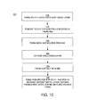
- FIGS. 1A, 1B, and 1C illustrate a flowchart of a process that is used in the fabrication of a semiconductor device according to embodiments of the present invention.
- FIGS. 2, 3, 4, 5, 6, 7, 8, 9, 10, 11, 12, 13, 14, 15, 16, 17, and 18 are cross-sectional views showing selected stages in the fabrication of a semiconductor device according to embodiments of the present invention.
- FIG. 19 is a cross-sectional view showing elements of a semiconductor device in an embodiment according to the present invention.
- n refers to an n-type dopant and the letter “p” refers to a p-type dopant.
- a plus sign “+” or a minus sign “ ⁇ ” is used to represent, respectively, a relatively high or relatively low concentration of the dopant.
- channel is used herein in the accepted manner. That is, current moves within a FET in a channel, from the source connection to the drain connection.
- a channel can be made of either n-type or p-type semiconductor material; accordingly, a FET is specified as either an n-channel or p-channel device.
- Some of the figures are discussed in the context of an n-channel device, specifically an n-channel power MOSFET; however, embodiments according to the present invention are not so limited. That is, the features described herein can be utilized in a p-channel device.
- the discussion of an n-channel device can be readily mapped to a p-channel device by substituting p-type dopant and materials for corresponding n-type dopant and materials, and vice versa.
- FIGS. 1A, 1B, and 1C illustrate a flowchart 100 of one embodiment of a process that is used in the fabrication of semiconductor devices such as the device partially illustrated in FIG. 19 .
- FIGS. 2-18 are cross-sectional views showing selected stages in the fabrication of a semiconductor device according to an embodiment of the present invention.
- an epitaxial (epi) layer 204 is grown over a substrate 202 (which may not be shown in subsequent figures).
- the epitaxial layer includes p-dopant and is grown over an n+ substrate.
- the structure includes a drain region 203 on the bottom surface of the substrate 202 .
- a photoresist (PR) mask 306 is formed over selected portions of the epi layer 204 . Then, the exposed portions of the epi layer 204 are etched away to form trench-like cavities, referred to as trenches 308 . The mask 306 is then removed, as shown in FIG. 4 .
- PR photoresist
- a thermal oxide layer 510 is produced (grown) over the epi layer 204 and along the sidewalls and bottom surfaces of the trenches 308 .
- the thermal oxide layer has a thickness of approximately 300 Angstroms (A).
- a dielectric layer 512 (also referred to herein as the first dielectric layer) is formed over the thermal oxide layer 510 , extending into the trenches 308 along their sidewalls and bottoms as shown in FIG. 5 .
- the dielectric layer 512 includes sub-atmospheric undoped silicon glass (SAUSG).
- SAUSG sub-atmospheric undoped silicon glass
- the thickness of the dielectric layer is approximately 1300 A.
- a first polysilicon layer 614 is formed over the dielectric layer 512 and into the trenches 308 (in FIG. 6 and subsequent figures, the dielectric layer 512 and the thermal oxide layer 510 may be represented as a single layer 511 ).
- the first polysilicon layer may also be referred to herein as poly-1.
- the poly-1 is removed using, for example, a chemical-mechanical planarization or polishing (CMP) process.
- CMP chemical-mechanical planarization or polishing
- the remaining poly-1 regions 714 can also be etched back a relatively small amount (e.g., about 0.1 microns) so that the exposed (e.g., top) surface of the poly-1 is slightly recessed relative to the layer 511 .
- a PR mask 816 is formed over selected poly-1 regions—that is, the core region of the structure is left exposed, while the pickup or termination region of the structure is covered by the mask 816 .
- the exposed poly-1 is etched back (recess etched) to form a poly-1 region 818 in the core region that fills the trench 308 to a lesser height than the poly-1 region 714 in the pickup or termination region.
- the PR mask 816 is removed, and then a blanket buffered oxide etch (BOE) is performed to remove portions of the layer 511 . More specifically, the layer 511 is removed along the mesas of the epi layer 204 , and from the sidewalls of the trenches 308 , partially exposing the sides of the poly-1 regions 714 and 818 as shown in FIG. 9 . The layer 511 is removed to a height that is slightly less than the height of the regions 714 and 818 .
- BOE blanket buffered oxide etch
- a dielectric layer 1020 is deposited over the exposed surfaces of the epi layer 204 and into the trenches 308 as shown in FIG. 10 using, for example, a sub-atmospheric pressure chemical vapor deposition (SACVD) process.
- the dielectric layer 1020 includes SAUSG (e.g., 6K SAUSG), which is densified. Any defects or voids in the surface of the poly-1 regions 714 and 818 will be filled when the recess is refilled with dielectric, thus achieving a proper profile instead of a distorted one.
- some of the dielectric layer 1020 is removed using a CMP process, for example, and the remainder of the dielectric layer is removed using a dry etch, such that the exposed surfaces of the epi layer 204 and the dielectric layer 1020 are planarized as shown in FIG. 11 .
- the same type of material e.g., SAUSG
- SAUSG is in the region above the poly-1 region 818 .
- a PR mask 1222 is formed over the pickup or termination region of the structure, leaving the core region exposed as shown in FIG. 12 .
- a proprietary oxide etch is then performed to remove a portion of the dielectric layer 1020 to form the dielectric layer 1226 (also referred to herein as the second dielectric layer). Because the same material is present throughout the dielectric layer 1020 , the problem of trying to achieve a uniform etch rate for different materials is avoided.
- the surface 1224 of the dielectric layer 1226 is curved.
- a cross-section of the structure is illustrated; in three dimensions, the surface 1224 of the dielectric layer 1226 is concave. Because the surface 1224 is curved, a sharp corner where the dielectric layer 1226 meets the sidewalls 1228 of the trench is thereby avoided.
- the PR mask 1222 is removed and a gate oxide layer 1330 is produced (grown) over the exposed surfaces of epi layer 204 , dielectric layer 1226 , and dielectric layer 1020 , as shown in FIG. 13 .
- the gate oxide layer 1330 will also be curved (concave-shaped) above the dielectric layer 1226 .
- the gate oxide retardation problem associated with the presence of sharp corners in conventional approaches, is avoided.
- a second polysilicon layer 1332 is then formed over the gate oxide layer 1330 .
- the second polysilicon layer may also be referred to herein as poly-2.
- the poly-2 is removed using, for example, a CMP process to form a poly-2 region 1434 .
- the poly-2 region 1434 can also be etched back a relatively small amount so that the exposed (e.g., top) surface of the poly-2 is slightly recessed relative to the gate oxide layer 1330 .
- the poly-1 region 818 and the poly-2 region 1434 correspond to the first and second electrodes of a split gate in a split gate power MOSFET, also known as a shielded gate trench MOSFET.
- a body implant is performed to form the body regions 1536 .
- the body regions 1536 include p-type (p-) dopant.
- a mask (not shown) can then be formed to shield the pickup or termination region, and then a source implant is performed to form the source region 1538 .
- the source region 1538 includes n-type (n+) dopant. The mask is then removed.
- a layer of low temperature oxide (LTO) followed by a layer of borophosphosilicate glass (BPSG) are deposited—these layers are collectively identified as layer 1640 in FIG. 16 .
- a mask (not shown) is used to selectively remove portions of the layer 1640 , the source region 1538 , and the body region 1536 , forming an opening 1742 .
- dopant is then implanted to form the p-type (p+) contact region 1744 .
- another mask (not shown) can be formed over selected areas and material can be removed beneath openings in the mask to form pickups (not shown) to the poly-1 regions 818 and 714 and the poly-2 region 1434 .
- a metal layer 1846 can be deposited over the structure as shown in FIG. 18 , and then another mask (not shown) can be formed to selectively remove portions of the metal layer to form electrical connections.
- a passivation layer (not shown) can be optionally deposited, and then another mask (not shown) can be applied to etch the passivation layer to define gate and source pads.
- FIG. 19 illustrates an embodiment of a trench or split gate 1900 .
- the gate 1900 includes a first electrode (e.g., polysilicon, poly-1) region 818 and a second electrode (e.g., polysilicon, poly-2) region 1434 that are separated from each other by a gate oxide layer 1330 that is adjacent to a second dielectric layer 1226 .
- the second dielectric layer 1226 is formed after the first dielectric layer 512 and separates the first dielectric layer 512 from the gate oxide layer 1330 .
- the boundary 1224 of the gate oxide layer 1330 and the second dielectric layer 1226 is curved.
- the boundary 1224 traverses the width of the gate trench 308 . More specifically, the boundary is concave in shape relative to the underlying dielectric layer 1226 (and therefore convex in shape relative to the gate oxide layer 1330 ).
Abstract
Description
Claims (13)
Priority Applications (9)
| Application Number | Priority Date | Filing Date | Title |
|---|---|---|---|
| US12/603,028 US9419129B2 (en) | 2009-10-21 | 2009-10-21 | Split gate semiconductor device with curved gate oxide profile |
| PCT/US2010/053617 WO2011050207A2 (en) | 2009-10-21 | 2010-10-21 | Split gate semiconductor device with curved gate oxide profile |
| CN201080056215.5A CN102656696B (en) | 2009-10-21 | 2010-10-21 | There is the sub-gate semiconductor device of arc gate oxide profile |
| EP10825703.1A EP2491593B1 (en) | 2009-10-21 | 2010-10-21 | Split gate semiconductor device with curved gate oxide profile |
| KR1020127009758A KR101493680B1 (en) | 2009-10-21 | 2010-10-21 | Split gate semiconductor device with curved gate oxide profile |
| JP2012535388A JP5932651B2 (en) | 2009-10-21 | 2010-10-21 | Split gate semiconductor device with curved gate oxide profile |
| US13/460,600 US20120220092A1 (en) | 2009-10-21 | 2012-04-30 | Method of forming a hybrid split gate simiconductor |
| US13/460,567 US20120211828A1 (en) | 2009-10-21 | 2012-04-30 | Hybrid split gate semiconductor |
| US15/237,259 US9893168B2 (en) | 2009-10-21 | 2016-08-15 | Split gate semiconductor device with curved gate oxide profile |
Applications Claiming Priority (1)
| Application Number | Priority Date | Filing Date | Title |
|---|---|---|---|
| US12/603,028 US9419129B2 (en) | 2009-10-21 | 2009-10-21 | Split gate semiconductor device with curved gate oxide profile |
Related Parent Applications (1)
| Application Number | Title | Priority Date | Filing Date |
|---|---|---|---|
| US12/869,554 Continuation-In-Part US9425305B2 (en) | 2009-10-20 | 2010-08-26 | Structures of and methods of fabricating split gate MIS devices |
Related Child Applications (3)
| Application Number | Title | Priority Date | Filing Date |
|---|---|---|---|
| US13/460,567 Continuation-In-Part US20120211828A1 (en) | 2009-10-21 | 2012-04-30 | Hybrid split gate semiconductor |
| US13/460,600 Continuation-In-Part US20120220092A1 (en) | 2009-10-21 | 2012-04-30 | Method of forming a hybrid split gate simiconductor |
| US15/237,259 Division US9893168B2 (en) | 2009-10-21 | 2016-08-15 | Split gate semiconductor device with curved gate oxide profile |
Publications (2)
| Publication Number | Publication Date |
|---|---|
| US20110089485A1 US20110089485A1 (en) | 2011-04-21 |
| US9419129B2 true US9419129B2 (en) | 2016-08-16 |
Family
ID=43878636
Family Applications (2)
| Application Number | Title | Priority Date | Filing Date |
|---|---|---|---|
| US12/603,028 Active US9419129B2 (en) | 2009-10-21 | 2009-10-21 | Split gate semiconductor device with curved gate oxide profile |
| US15/237,259 Active US9893168B2 (en) | 2009-10-21 | 2016-08-15 | Split gate semiconductor device with curved gate oxide profile |
Family Applications After (1)
| Application Number | Title | Priority Date | Filing Date |
|---|---|---|---|
| US15/237,259 Active US9893168B2 (en) | 2009-10-21 | 2016-08-15 | Split gate semiconductor device with curved gate oxide profile |
Country Status (6)
| Country | Link |
|---|---|
| US (2) | US9419129B2 (en) |
| EP (1) | EP2491593B1 (en) |
| JP (1) | JP5932651B2 (en) |
| KR (1) | KR101493680B1 (en) |
| CN (1) | CN102656696B (en) |
| WO (1) | WO2011050207A2 (en) |
Cited By (1)
| Publication number | Priority date | Publication date | Assignee | Title |
|---|---|---|---|---|
| US20160064477A1 (en) * | 2014-08-28 | 2016-03-03 | Infineon Technologies Austria Ag | Semiconductor Device and a Method for Manufacturing a Semiconductor Device |
Families Citing this family (43)
| Publication number | Priority date | Publication date | Assignee | Title |
|---|---|---|---|---|
| US6838722B2 (en) * | 2002-03-22 | 2005-01-04 | Siliconix Incorporated | Structures of and methods of fabricating trench-gated MIS devices |
| US9425305B2 (en) | 2009-10-20 | 2016-08-23 | Vishay-Siliconix | Structures of and methods of fabricating split gate MIS devices |
| US9419129B2 (en) | 2009-10-21 | 2016-08-16 | Vishay-Siliconix | Split gate semiconductor device with curved gate oxide profile |
| US9577089B2 (en) | 2010-03-02 | 2017-02-21 | Vishay-Siliconix | Structures and methods of fabricating dual gate devices |
| TWI453831B (en) | 2010-09-09 | 2014-09-21 | 台灣捷康綜合有限公司 | Semiconductor package and method for making the same |
| WO2012158977A2 (en) | 2011-05-18 | 2012-11-22 | Vishay-Siliconix | Semiconductor device |
| KR20150003775A (en) * | 2012-04-30 | 2015-01-09 | 비쉐이-실리코닉스 | Semiconductor device |
| CN104380441A (en) * | 2012-04-30 | 2015-02-25 | 维西埃-硅化物公司 | Integrated circuit design |
| US9589929B2 (en) | 2013-03-14 | 2017-03-07 | Vishay-Siliconix | Method for fabricating stack die package |
| US9966330B2 (en) | 2013-03-14 | 2018-05-08 | Vishay-Siliconix | Stack die package |
| JP5784665B2 (en) * | 2013-03-22 | 2015-09-24 | 株式会社東芝 | Manufacturing method of semiconductor device |
| JP6177154B2 (en) * | 2013-07-16 | 2017-08-09 | 株式会社東芝 | Semiconductor device |
| JP2016040820A (en) | 2013-09-20 | 2016-03-24 | サンケン電気株式会社 | Semiconductor device |
| JP6173987B2 (en) | 2013-09-20 | 2017-08-02 | サンケン電気株式会社 | Semiconductor device |
| CN204102904U (en) | 2013-09-20 | 2015-01-14 | 三垦电气株式会社 | Semiconductor device |
| CN104701148B (en) * | 2013-12-04 | 2017-11-24 | 和舰科技(苏州)有限公司 | The manufacture method of splitting bar |
| EP3183753A4 (en) | 2014-08-19 | 2018-01-10 | Vishay-Siliconix | Electronic circuit |
| US9425304B2 (en) | 2014-08-21 | 2016-08-23 | Vishay-Siliconix | Transistor structure with improved unclamped inductive switching immunity |
| CN105957811A (en) * | 2016-04-27 | 2016-09-21 | 上海华虹宏力半导体制造有限公司 | Method for manufacturing trench gate power devices with shielded gate |
| TWI577010B (en) | 2016-05-18 | 2017-04-01 | 杰力科技股份有限公司 | Power mosfet |
| TWI615889B (en) | 2016-05-18 | 2018-02-21 | 杰力科技股份有限公司 | Method of fabricating power mosfet |
| CN106298945A (en) * | 2016-09-30 | 2017-01-04 | 上海华虹宏力半导体制造有限公司 | Shield grid trench MOSFET process |
| CN107731923B (en) * | 2017-09-02 | 2019-09-03 | 西安交通大学 | The silicon carbide super-junction MOSFET device and preparation method of a kind of low on-resistance, small grid charge |
| CN107799602A (en) * | 2017-10-24 | 2018-03-13 | 贵州芯长征科技有限公司 | Shielding grid MOSFET component of terminal area and preparation method thereof can be saved |
| CN107910267B (en) * | 2017-11-17 | 2023-09-08 | 杭州士兰集成电路有限公司 | Power semiconductor device and method of manufacturing the same |
| CN107910270A (en) * | 2017-11-17 | 2018-04-13 | 杭州士兰集成电路有限公司 | Power semiconductor and its manufacture method |
| CN108417637A (en) * | 2018-03-09 | 2018-08-17 | 香港商莫斯飞特半导体股份有限公司 | A kind of more groove semiconductor power devices and preparation method thereof |
| CN109037337A (en) * | 2018-06-28 | 2018-12-18 | 华为技术有限公司 | A kind of power semiconductor and manufacturing method |
| CN110047759A (en) * | 2019-04-28 | 2019-07-23 | 矽力杰半导体技术(杭州)有限公司 | Trench MOSFET device manufacturing method |
| US11217541B2 (en) | 2019-05-08 | 2022-01-04 | Vishay-Siliconix, LLC | Transistors with electrically active chip seal ring and methods of manufacture |
| US11218144B2 (en) | 2019-09-12 | 2022-01-04 | Vishay-Siliconix, LLC | Semiconductor device with multiple independent gates |
| CN113053738A (en) * | 2019-12-27 | 2021-06-29 | 华润微电子(重庆)有限公司 | Split gate type groove MOS device and preparation method thereof |
| CN111081540A (en) * | 2019-12-30 | 2020-04-28 | 广州粤芯半导体技术有限公司 | Manufacturing method of shielded gate trench power device |
| CN113130633B (en) * | 2019-12-30 | 2022-11-22 | 华润微电子(重庆)有限公司 | Groove type field effect transistor structure and preparation method thereof |
| CN111681963B (en) * | 2020-08-11 | 2020-11-20 | 中芯集成电路制造(绍兴)有限公司 | Shielded gate field effect transistor and forming method thereof |
| CN112509979B (en) * | 2020-11-30 | 2022-08-09 | 绍兴中芯集成电路制造股份有限公司 | Semiconductor device having a shielded gate trench structure and method of fabricating the same |
| CN112509980B (en) * | 2020-11-30 | 2022-06-03 | 绍兴中芯集成电路制造股份有限公司 | Semiconductor device having a shielded gate trench structure and method of manufacturing the same |
| CN112701043A (en) * | 2020-12-28 | 2021-04-23 | 广州粤芯半导体技术有限公司 | Method for manufacturing semiconductor device |
| CN113192825A (en) * | 2021-04-26 | 2021-07-30 | 广州粤芯半导体技术有限公司 | Manufacturing method of split-gate trench power device |
| CN113471278A (en) * | 2021-06-24 | 2021-10-01 | 无锡新洁能股份有限公司 | Shielded gate trench type semiconductor device and method of manufacturing the same |
| CN114420637B (en) * | 2021-12-22 | 2023-12-29 | 深圳深爱半导体股份有限公司 | Semiconductor device structure and preparation method thereof |
| CN114496762A (en) * | 2022-04-13 | 2022-05-13 | 杭州芯迈半导体技术有限公司 | Method for manufacturing trench MOSFET |
| CN114975126B (en) * | 2022-07-29 | 2022-10-25 | 威晟半导体科技(广州)有限公司 | Manufacturing method of shielded gate trench type MOSFET (Metal-oxide-semiconductor field Effect transistor) capable of reducing gate charges |
Citations (98)
| Publication number | Priority date | Publication date | Assignee | Title |
|---|---|---|---|---|
| JPS63296282A (en) | 1987-05-27 | 1988-12-02 | Sony Corp | Semiconductor device |
| JPH03211885A (en) | 1990-01-17 | 1991-09-17 | Matsushita Electron Corp | Semiconductor device and manufacture thereof |
| WO1994003922A1 (en) | 1992-08-07 | 1994-02-17 | Advanced Power Technology, Inc. | High density power device structure and fabrication process |
| JPH0745817A (en) | 1993-07-27 | 1995-02-14 | Nissan Motor Co Ltd | Insulated electrode and its manufacture |
| JPH07235676A (en) | 1994-02-24 | 1995-09-05 | Mitsubishi Electric Corp | Semiconductor device and manufacture thereof |
| EP0717450A2 (en) | 1994-12-13 | 1996-06-19 | Mitsubishi Denki Kabushiki Kaisha | Vertiacal insulated gate semiconductor device and method of manufacturing the same |
| JPH10173175A (en) | 1996-12-09 | 1998-06-26 | Toshiba Corp | Semiconductor device and its manufacture |
| JPH1168102A (en) | 1997-08-21 | 1999-03-09 | Toshiba Corp | Production of semiconductor device |
| US6031265A (en) | 1997-10-16 | 2000-02-29 | Magepower Semiconductor Corp. | Enhancing DMOS device ruggedness by reducing transistor parasitic resistance and by inducing breakdown near gate runners and termination area |
| WO2000025363A1 (en) | 1998-10-23 | 2000-05-04 | Stmicroelectronics S.A. | Power component bearing interconnections |
| WO2000042665A1 (en) | 1999-01-11 | 2000-07-20 | Fraunhofer-Gesellschaft zur Förderung der angewandten Forschung e.V. | Power mos element and method for producing the same |
| JP2000223705A (en) | 1999-01-29 | 2000-08-11 | Nissan Motor Co Ltd | Semiconductor device |
| WO2000065646A1 (en) | 1999-04-22 | 2000-11-02 | Williams Richard K | A super-self-aligned trench-gate dmos with reduced on-resistance |
| US6242775B1 (en) | 1998-02-24 | 2001-06-05 | Micron Technology, Inc. | Circuits and methods using vertical complementary transistors |
| WO2000051167A9 (en) | 1999-02-26 | 2001-06-14 | Fairchild Semiconductor | Monolithically integrated trench mosfet and schottky diode |
| US6255683B1 (en) | 1998-12-29 | 2001-07-03 | Infineon Technologies Ag | Dynamic random access memory |
| US6281547B1 (en) | 1997-05-08 | 2001-08-28 | Megamos Corporation | Power transistor cells provided with reliable trenched source contacts connected to narrower source manufactured without a source mask |
| WO2000025365A3 (en) | 1998-10-26 | 2001-09-07 | Univ North Carolina State | Power semiconductor devices having improved high frequency switching and breakdown characteristics |
| US6291298B1 (en) * | 1999-05-25 | 2001-09-18 | Advanced Analogic Technologies, Inc. | Process of manufacturing Trench gate semiconductor device having gate oxide layer with multiple thicknesses |
| US6309929B1 (en) | 2000-09-22 | 2001-10-30 | Industrial Technology Research Institute And Genetal Semiconductor Of Taiwan, Ltd. | Method of forming trench MOS device and termination structure |
| JP2001308327A (en) | 2000-04-26 | 2001-11-02 | Fuji Electric Co Ltd | Insulated gate semiconductor device |
| US20020036319A1 (en) | 1998-10-26 | 2002-03-28 | Baliga Bantval Jayant | Vertical MOSFETs having trench-based gate electrodes within deeper trench-based source electrodes and methods of forming same |
| JP2002110984A (en) | 2000-06-08 | 2002-04-12 | Siliconix Inc | High-frequency mosfet and manufacturing method thereof |
| US20020056884A1 (en) | 2000-11-16 | 2002-05-16 | Baliga Bantval Jayant | Vertical power devices having deep and shallow trenches and methods of forming same |
| US6404007B1 (en) * | 1999-04-05 | 2002-06-11 | Fairchild Semiconductor Corporation | Trench transistor with superior gate dielectric |
| US6489204B1 (en) | 2001-08-20 | 2002-12-03 | Episil Technologies, Inc. | Save MOS device |
| US6495884B2 (en) | 2000-03-22 | 2002-12-17 | Seiko Instruments Inc. | Vertical MOS transistor |
| US6525373B1 (en) | 1998-06-30 | 2003-02-25 | Fairchild Korea Semiconductor Ltd. | Power semiconductor device having trench gate structure and method for manufacturing the same |
| US6545315B2 (en) | 1999-09-14 | 2003-04-08 | General Semiconductor, Inc. | Trench DMOS transistor having reduced punch-through |
| US6548860B1 (en) | 2000-02-29 | 2003-04-15 | General Semiconductor, Inc. | DMOS transistor structure having improved performance |
| US20030086296A1 (en) | 2001-04-24 | 2003-05-08 | Meng-Yi Wu | Method of forming and operating trench split gate non-volatile flash memory cell structure |
| US6621107B2 (en) | 2001-08-23 | 2003-09-16 | General Semiconductor, Inc. | Trench DMOS transistor with embedded trench schottky rectifier |
| US20030178676A1 (en) | 2002-03-19 | 2003-09-25 | Ralf Henninger | Transistor configuration with a shielding electrode outside an active cell array and a reduced gate-drain capacitance |
| JP2003282870A (en) | 2002-03-20 | 2003-10-03 | Fuji Electric Co Ltd | Semiconductor device and its fabricating method |
| US20030201502A1 (en) | 2002-02-26 | 2003-10-30 | Taiwan Semiconductor Manufacturing Company | Method to fabricate self-aligned source and drain in split gate flash |
| JP2003309263A (en) | 2002-03-22 | 2003-10-31 | Siliconix Inc | Structure of trench gate mis device and its manufacturing method |
| US6683346B2 (en) | 2001-03-09 | 2004-01-27 | Fairchild Semiconductor Corporation | Ultra dense trench-gated power-device with the reduced drain-source feedback capacitance and Miller charge |
| US20040021173A1 (en) | 2002-07-30 | 2004-02-05 | Fairchild Semiconductor Corporation | Dual trench power mosfet |
| US20040038479A1 (en) | 2002-08-20 | 2004-02-26 | Taiwan Semiconductor Manufacturing Company | Structure and fabricating method with self-aligned bit line contact to word line in split gate flash |
| US6707128B2 (en) | 2001-06-13 | 2004-03-16 | Kabushiki Kaisha Toshiba | Vertical MISFET transistor surrounded by a Schottky barrier diode with a common source and anode electrode |
| US20040084721A1 (en) | 2002-11-05 | 2004-05-06 | Fairchild Semiconductor Corporation | Trench structure having one or more diodes embedded therein adjacent a PN junction and method of forming the same |
| US20040113202A1 (en) | 2002-08-23 | 2004-06-17 | Kocon Christopher B. | Method and apparatus for improved MOS gating to reduce miller capacitance and switching losses |
| US6781199B2 (en) | 2001-05-29 | 2004-08-24 | Mitsubishi Denki Kabushiki Kaisha | Semiconductor device having first and second trenches with no control electrode formed in the second trench |
| JP2004241413A (en) | 2003-02-03 | 2004-08-26 | Toshiba Corp | Semiconductor device |
| US20050001268A1 (en) | 2000-06-23 | 2005-01-06 | Baliga Bantval Jayant | Power semiconductor devices having linear transfer characteristics when regions therein are in velocity saturation modes and methods of forming and operating same |
| JP2005032941A (en) | 2003-07-11 | 2005-02-03 | Fuji Electric Device Technology Co Ltd | Insulated gate type semiconductor device |
| JP2005057050A (en) | 2003-08-04 | 2005-03-03 | Renesas Technology Corp | Semiconductor device and its manufacturing method |
| US20050079676A1 (en) | 1997-11-14 | 2005-04-14 | Fairchild Semiconductor Corporation | Method of manufacturing a trench transistor having a heavy body region |
| US6882000B2 (en) | 2001-08-10 | 2005-04-19 | Siliconix Incorporated | Trench MIS device with reduced gate-to-drain capacitance |
| US20050082591A1 (en) * | 2003-08-27 | 2005-04-21 | Infineon Technologies Ag | Vertical semiconductor component having a drift zone having a field electrode, and method for fabricating such a drift zone |
| US6906380B1 (en) | 2004-05-13 | 2005-06-14 | Vishay-Siliconix | Drain side gate trench metal-oxide-semiconductor field effect transistor |
| JP2005191221A (en) | 2003-12-25 | 2005-07-14 | Toshiba Corp | Semiconductor device |
| US20050151190A1 (en) | 2003-11-14 | 2005-07-14 | Infineon Technologies Ag | Power transistor arrangement and method for fabricating it |
| US20050167742A1 (en) * | 2001-01-30 | 2005-08-04 | Fairchild Semiconductor Corp. | Power semiconductor devices and methods of manufacture |
| US20060017056A1 (en) | 2004-06-18 | 2006-01-26 | Infineon Technologies Ag | Field plate trench transistor |
| US7009247B2 (en) | 2001-07-03 | 2006-03-07 | Siliconix Incorporated | Trench MIS device with thick oxide layer in bottom of gate contact trench |
| WO2005065385A3 (en) | 2003-12-30 | 2006-04-06 | Fairchild Semiconductor | Power semiconductor devices and methods of manufacture |
| US20060113577A1 (en) | 2004-09-28 | 2006-06-01 | Nec Electronics Corporation | Semiconductor device |
| JP2006202931A (en) | 2005-01-20 | 2006-08-03 | Renesas Technology Corp | Semiconductor device and its manufacturing method |
| US20060209887A1 (en) | 2005-02-11 | 2006-09-21 | Alpha & Omega Semiconductor, Ltd | Shielded gate trench (SGT) MOSFET cells implemented with a schottky source contact |
| US20060214221A1 (en) | 2003-05-20 | 2006-09-28 | Ashok Challa | Power semiconductor devices and methods of manufacture |
| WO2006127914A2 (en) | 2005-05-26 | 2006-11-30 | Fairchild Semiconductor Corporation | Trench-gate field effect transistors and methods of forming the same |
| US20060281249A1 (en) * | 2005-06-10 | 2006-12-14 | Hamza Yilmaz | Charge balance field effect transistor |
| US20070004116A1 (en) | 2005-06-06 | 2007-01-04 | M-Mos Semiconductor Sdn. Bhd. | Trenched MOSFET termination with tungsten plug structures |
| US20070037327A1 (en) * | 2005-08-09 | 2007-02-15 | Robert Herrick | Structure and method for forming inter-poly dielectric in a shielded gate field effect transistor |
| DE102005041322A1 (en) | 2005-08-31 | 2007-03-01 | Infineon Technologies Ag | Trench transistor structure, with a field electrode array in the trenches, has a potential fixed for the field electrodes through semiconductor zones |
| US20070108511A1 (en) | 2005-10-06 | 2007-05-17 | Infineon Technologies Austria Ag | Semiconductor structure, method for operating a semiconductor structure and method for producing a semiconductor structure |
| US20070108515A1 (en) | 2003-11-29 | 2007-05-17 | Koninklijke Philips Electronics, N.V. | Trench mosfet |
| US20070132014A1 (en) | 2003-11-29 | 2007-06-14 | Koninklijke Philips Electronics N.V. | Trench insulated gate field effect transistor |
| US20070155104A1 (en) | 2006-01-05 | 2007-07-05 | Marchant Bruce D | Power device utilizing chemical mechanical planarization |
| US20070221952A1 (en) | 2006-03-24 | 2007-09-27 | Paul Thorup | High density trench FET with integrated Schottky diode and method of manufacture |
| WO2007129261A3 (en) | 2006-05-05 | 2008-01-10 | Koninkl Philips Electronics Nv | Trench field effect transistors |
| US20080076222A1 (en) | 2006-09-26 | 2008-03-27 | Infineon Technologies Austria Ag | Method for producing an integrated circuit with a trench transistor structure |
| US20080073707A1 (en) | 2006-09-27 | 2008-03-27 | Darwish Mohamed N | Power MOSFET with recessed field plate |
| US20080135889A1 (en) | 2006-12-06 | 2008-06-12 | Fred Session | Structure and Method for Forming a Planar Schottky Contact |
| US20080166845A1 (en) | 2007-01-09 | 2008-07-10 | Maxpower Semiconductor, Inc. | Method of manufacture for a semiconductor device |
| US20080265289A1 (en) | 2007-04-30 | 2008-10-30 | Alpha & Omega Semiconductor, Ltd | Device structure and manufacturing method using HDP deposited source-body implant block |
| JP2008543046A (en) | 2005-05-24 | 2008-11-27 | ヴィシェイ−シリコニックス | Trench-type metal oxide semiconductor field effect transistor |
| US7494876B1 (en) | 2005-04-21 | 2009-02-24 | Vishay Siliconix | Trench-gated MIS device having thick polysilicon insulation layer at trench bottom and method of fabricating the same |
| WO2009026174A1 (en) | 2007-08-21 | 2009-02-26 | Fairchild Semiconductor Corporation | Method and structure for shielded gate trench fet |
| US20090057756A1 (en) | 2006-09-26 | 2009-03-05 | Force-Mos Technology Corporation | Trench MOSFET with Trench Termination and manufacture thereof |
| US7544571B2 (en) | 2006-09-20 | 2009-06-09 | Fairchild Semiconductor Corporation | Trench gate FET with self-aligned features |
| JP2009141005A (en) | 2007-12-04 | 2009-06-25 | Rohm Co Ltd | Semiconductor device, and method for manufacturing the same |
| US20090162989A1 (en) | 2007-12-21 | 2009-06-25 | Samsung Electronics Co. Ltd. | Methods of manufacturing a semiconductor device using a layer suspended across a trench |
| US20090273026A1 (en) | 2002-10-03 | 2009-11-05 | Wilson Peter H | Trench-gate ldmos structures |
| JP2009542002A (en) | 2006-06-19 | 2009-11-26 | フェアチャイルド・セミコンダクター・コーポレーション | Structure of shield gate trench FET having shield electrode and gate electrode connected to each other and method of forming the same |
| US20090309156A1 (en) | 2008-06-11 | 2009-12-17 | Maxpower Semiconductor Inc. | Super Self-Aligned Trench MOSFET Devices, Methods, and Systems |
| US20100006928A1 (en) * | 2008-07-09 | 2010-01-14 | James Pan | Structure and Method for Forming a Shielded Gate Trench FET with an Inter-electrode Dielectric Having a Low-k Dielectric Therein |
| US20110079843A1 (en) | 2009-04-13 | 2011-04-07 | Maxpower Semiconductor, Inc. | POWER SEMICONDUCTOR DEVICES, METHODS, AND STRUCTURES WITH Embedded Dielectric Layers Containing Permanent Charges |
| US20110089485A1 (en) | 2009-10-21 | 2011-04-21 | Vishay-Siliconix | Split gate semiconductor device with curved gate oxide profile |
| WO2011050115A2 (en) | 2009-10-20 | 2011-04-28 | Vishay-Siliconix | Split gate field effect transistor |
| JP2011258834A (en) | 2010-06-10 | 2011-12-22 | Fuji Electric Co Ltd | Semiconductor device and method of manufacturing the same |
| US20120043602A1 (en) | 2010-01-11 | 2012-02-23 | Maxpower Semiconductor Inc. | Power MOSFET and Its Edge Termination |
| US20120061753A1 (en) | 2010-09-09 | 2012-03-15 | Kabushiki Kaisha Toshiba | Semiconductor device |
| US20120267704A1 (en) | 2011-04-22 | 2012-10-25 | Infineon Technologies Ag | Transistor arrangement with a mosfet |
| US20130049072A1 (en) | 2011-08-25 | 2013-02-28 | Lars P. Heineck | Arrays Of Recessed Access Devices, Methods Of Forming Recessed Access Gate Constructions, And Methods Of Forming Isolation Gate Constructions In The Fabrication Of Recessed Access Devices |
| US20130221436A1 (en) | 2012-02-24 | 2013-08-29 | Zia Hossain | Electronic device including a trench and a conductive structure therein and a process of forming the same |
| US8686493B2 (en) | 2007-10-04 | 2014-04-01 | Fairchild Semiconductor Corporation | High density FET with integrated Schottky |
Family Cites Families (3)
| Publication number | Priority date | Publication date | Assignee | Title |
|---|---|---|---|---|
| JP2009135360A (en) | 2007-12-03 | 2009-06-18 | Renesas Technology Corp | Semiconductor device and its manufacturing method |
| CN104380441A (en) | 2012-04-30 | 2015-02-25 | 维西埃-硅化物公司 | Integrated circuit design |
| KR20150003775A (en) | 2012-04-30 | 2015-01-09 | 비쉐이-실리코닉스 | Semiconductor device |
-
2009
- 2009-10-21 US US12/603,028 patent/US9419129B2/en active Active
-
2010
- 2010-10-21 EP EP10825703.1A patent/EP2491593B1/en active Active
- 2010-10-21 KR KR1020127009758A patent/KR101493680B1/en active IP Right Grant
- 2010-10-21 JP JP2012535388A patent/JP5932651B2/en active Active
- 2010-10-21 CN CN201080056215.5A patent/CN102656696B/en active Active
- 2010-10-21 WO PCT/US2010/053617 patent/WO2011050207A2/en active Application Filing
-
2016
- 2016-08-15 US US15/237,259 patent/US9893168B2/en active Active
Patent Citations (129)
| Publication number | Priority date | Publication date | Assignee | Title |
|---|---|---|---|---|
| JPS63296282A (en) | 1987-05-27 | 1988-12-02 | Sony Corp | Semiconductor device |
| JPH03211885A (en) | 1990-01-17 | 1991-09-17 | Matsushita Electron Corp | Semiconductor device and manufacture thereof |
| WO1994003922A1 (en) | 1992-08-07 | 1994-02-17 | Advanced Power Technology, Inc. | High density power device structure and fabrication process |
| JPH0745817A (en) | 1993-07-27 | 1995-02-14 | Nissan Motor Co Ltd | Insulated electrode and its manufacture |
| JPH07235676A (en) | 1994-02-24 | 1995-09-05 | Mitsubishi Electric Corp | Semiconductor device and manufacture thereof |
| EP0717450A2 (en) | 1994-12-13 | 1996-06-19 | Mitsubishi Denki Kabushiki Kaisha | Vertiacal insulated gate semiconductor device and method of manufacturing the same |
| JPH08167711A (en) | 1994-12-13 | 1996-06-25 | Mitsubishi Electric Corp | Insulated gate semiconductor device and manufacture thereof |
| US5864159A (en) | 1994-12-13 | 1999-01-26 | Mitsubishi Denki Kabushiki Kaisha | Insulated gate semiconductor device structure to prevent a reduction in breakdown voltage |
| JPH10173175A (en) | 1996-12-09 | 1998-06-26 | Toshiba Corp | Semiconductor device and its manufacture |
| US6281547B1 (en) | 1997-05-08 | 2001-08-28 | Megamos Corporation | Power transistor cells provided with reliable trenched source contacts connected to narrower source manufactured without a source mask |
| JPH1168102A (en) | 1997-08-21 | 1999-03-09 | Toshiba Corp | Production of semiconductor device |
| US6031265A (en) | 1997-10-16 | 2000-02-29 | Magepower Semiconductor Corp. | Enhancing DMOS device ruggedness by reducing transistor parasitic resistance and by inducing breakdown near gate runners and termination area |
| US20050079676A1 (en) | 1997-11-14 | 2005-04-14 | Fairchild Semiconductor Corporation | Method of manufacturing a trench transistor having a heavy body region |
| US6242775B1 (en) | 1998-02-24 | 2001-06-05 | Micron Technology, Inc. | Circuits and methods using vertical complementary transistors |
| US6525373B1 (en) | 1998-06-30 | 2003-02-25 | Fairchild Korea Semiconductor Ltd. | Power semiconductor device having trench gate structure and method for manufacturing the same |
| WO2000025363A1 (en) | 1998-10-23 | 2000-05-04 | Stmicroelectronics S.A. | Power component bearing interconnections |
| WO2000025365A3 (en) | 1998-10-26 | 2001-09-07 | Univ North Carolina State | Power semiconductor devices having improved high frequency switching and breakdown characteristics |
| US20020036319A1 (en) | 1998-10-26 | 2002-03-28 | Baliga Bantval Jayant | Vertical MOSFETs having trench-based gate electrodes within deeper trench-based source electrodes and methods of forming same |
| US6255683B1 (en) | 1998-12-29 | 2001-07-03 | Infineon Technologies Ag | Dynamic random access memory |
| WO2000042665A1 (en) | 1999-01-11 | 2000-07-20 | Fraunhofer-Gesellschaft zur Förderung der angewandten Forschung e.V. | Power mos element and method for producing the same |
| US6462376B1 (en) | 1999-01-11 | 2002-10-08 | Fraunhofer-Gesellschaft Zur Foerderung Der Angewandten Forschung E.V. | Power MOS element and method for producing the same |
| JP2000223705A (en) | 1999-01-29 | 2000-08-11 | Nissan Motor Co Ltd | Semiconductor device |
| WO2000051167A9 (en) | 1999-02-26 | 2001-06-14 | Fairchild Semiconductor | Monolithically integrated trench mosfet and schottky diode |
| US6404007B1 (en) * | 1999-04-05 | 2002-06-11 | Fairchild Semiconductor Corporation | Trench transistor with superior gate dielectric |
| WO2000065646A1 (en) | 1999-04-22 | 2000-11-02 | Williams Richard K | A super-self-aligned trench-gate dmos with reduced on-resistance |
| US6413822B2 (en) | 1999-04-22 | 2002-07-02 | Advanced Analogic Technologies, Inc. | Super-self-aligned fabrication process of trench-gate DMOS with overlying device layer |
| US6291298B1 (en) * | 1999-05-25 | 2001-09-18 | Advanced Analogic Technologies, Inc. | Process of manufacturing Trench gate semiconductor device having gate oxide layer with multiple thicknesses |
| US6900100B2 (en) * | 1999-05-25 | 2005-05-31 | Advanced Analogic Technologies, Inc. | Trench semiconductor device having gate oxide layer with multiple thicknesses and processes of fabricating the same |
| US6545315B2 (en) | 1999-09-14 | 2003-04-08 | General Semiconductor, Inc. | Trench DMOS transistor having reduced punch-through |
| US6548860B1 (en) | 2000-02-29 | 2003-04-15 | General Semiconductor, Inc. | DMOS transistor structure having improved performance |
| US6495884B2 (en) | 2000-03-22 | 2002-12-17 | Seiko Instruments Inc. | Vertical MOS transistor |
| JP2001308327A (en) | 2000-04-26 | 2001-11-02 | Fuji Electric Co Ltd | Insulated gate semiconductor device |
| JP2002110984A (en) | 2000-06-08 | 2002-04-12 | Siliconix Inc | High-frequency mosfet and manufacturing method thereof |
| US20050001268A1 (en) | 2000-06-23 | 2005-01-06 | Baliga Bantval Jayant | Power semiconductor devices having linear transfer characteristics when regions therein are in velocity saturation modes and methods of forming and operating same |
| US6309929B1 (en) | 2000-09-22 | 2001-10-30 | Industrial Technology Research Institute And Genetal Semiconductor Of Taiwan, Ltd. | Method of forming trench MOS device and termination structure |
| US20020056884A1 (en) | 2000-11-16 | 2002-05-16 | Baliga Bantval Jayant | Vertical power devices having deep and shallow trenches and methods of forming same |
| US7345342B2 (en) | 2001-01-30 | 2008-03-18 | Fairchild Semiconductor Corporation | Power semiconductor devices and methods of manufacture |
| US20050167742A1 (en) * | 2001-01-30 | 2005-08-04 | Fairchild Semiconductor Corp. | Power semiconductor devices and methods of manufacture |
| US6683346B2 (en) | 2001-03-09 | 2004-01-27 | Fairchild Semiconductor Corporation | Ultra dense trench-gated power-device with the reduced drain-source feedback capacitance and Miller charge |
| US20030086296A1 (en) | 2001-04-24 | 2003-05-08 | Meng-Yi Wu | Method of forming and operating trench split gate non-volatile flash memory cell structure |
| US6781199B2 (en) | 2001-05-29 | 2004-08-24 | Mitsubishi Denki Kabushiki Kaisha | Semiconductor device having first and second trenches with no control electrode formed in the second trench |
| US6707128B2 (en) | 2001-06-13 | 2004-03-16 | Kabushiki Kaisha Toshiba | Vertical MISFET transistor surrounded by a Schottky barrier diode with a common source and anode electrode |
| US7009247B2 (en) | 2001-07-03 | 2006-03-07 | Siliconix Incorporated | Trench MIS device with thick oxide layer in bottom of gate contact trench |
| US6921697B2 (en) | 2001-08-10 | 2005-07-26 | Siliconix Incorporated | Method for making trench MIS device with reduced gate-to-drain capacitance |
| US6882000B2 (en) | 2001-08-10 | 2005-04-19 | Siliconix Incorporated | Trench MIS device with reduced gate-to-drain capacitance |
| US6489204B1 (en) | 2001-08-20 | 2002-12-03 | Episil Technologies, Inc. | Save MOS device |
| US6621107B2 (en) | 2001-08-23 | 2003-09-16 | General Semiconductor, Inc. | Trench DMOS transistor with embedded trench schottky rectifier |
| US20030201502A1 (en) | 2002-02-26 | 2003-10-30 | Taiwan Semiconductor Manufacturing Company | Method to fabricate self-aligned source and drain in split gate flash |
| US20030178676A1 (en) | 2002-03-19 | 2003-09-25 | Ralf Henninger | Transistor configuration with a shielding electrode outside an active cell array and a reduced gate-drain capacitance |
| JP2003282870A (en) | 2002-03-20 | 2003-10-03 | Fuji Electric Co Ltd | Semiconductor device and its fabricating method |
| US7335946B1 (en) | 2002-03-22 | 2008-02-26 | Vishay-Siliconix | Structures of and methods of fabricating trench-gated MIS devices |
| US6838722B2 (en) | 2002-03-22 | 2005-01-04 | Siliconix Incorporated | Structures of and methods of fabricating trench-gated MIS devices |
| JP2003309263A (en) | 2002-03-22 | 2003-10-31 | Siliconix Inc | Structure of trench gate mis device and its manufacturing method |
| US7868381B1 (en) | 2002-03-22 | 2011-01-11 | Vishay-Siliconix | Structures of and methods of fabricating trench-gated MIS devices |
| US7005347B1 (en) | 2002-03-22 | 2006-02-28 | Vishay-Siliconix | Structures of and methods of fabricating trench-gated MIS devices |
| US20040021173A1 (en) | 2002-07-30 | 2004-02-05 | Fairchild Semiconductor Corporation | Dual trench power mosfet |
| US20040038479A1 (en) | 2002-08-20 | 2004-02-26 | Taiwan Semiconductor Manufacturing Company | Structure and fabricating method with self-aligned bit line contact to word line in split gate flash |
| US20040113202A1 (en) | 2002-08-23 | 2004-06-17 | Kocon Christopher B. | Method and apparatus for improved MOS gating to reduce miller capacitance and switching losses |
| US20090273026A1 (en) | 2002-10-03 | 2009-11-05 | Wilson Peter H | Trench-gate ldmos structures |
| US20040084721A1 (en) | 2002-11-05 | 2004-05-06 | Fairchild Semiconductor Corporation | Trench structure having one or more diodes embedded therein adjacent a PN junction and method of forming the same |
| JP2004241413A (en) | 2003-02-03 | 2004-08-26 | Toshiba Corp | Semiconductor device |
| US20080199997A1 (en) | 2003-05-20 | 2008-08-21 | Grebs Thomas E | Methods of Forming Inter-poly Dielectric (IPD) Layers in Power Semiconductor Devices |
| US20080197407A1 (en) | 2003-05-20 | 2008-08-21 | Ashok Challa | Power Semiconductor Devices with Barrier Layer to Reduce Substrate Up-Diffusion and Methods of Manufacture |
| US20060214221A1 (en) | 2003-05-20 | 2006-09-28 | Ashok Challa | Power semiconductor devices and methods of manufacture |
| JP2005032941A (en) | 2003-07-11 | 2005-02-03 | Fuji Electric Device Technology Co Ltd | Insulated gate type semiconductor device |
| JP2005057050A (en) | 2003-08-04 | 2005-03-03 | Renesas Technology Corp | Semiconductor device and its manufacturing method |
| US20050082591A1 (en) * | 2003-08-27 | 2005-04-21 | Infineon Technologies Ag | Vertical semiconductor component having a drift zone having a field electrode, and method for fabricating such a drift zone |
| US20050151190A1 (en) | 2003-11-14 | 2005-07-14 | Infineon Technologies Ag | Power transistor arrangement and method for fabricating it |
| US20070108515A1 (en) | 2003-11-29 | 2007-05-17 | Koninklijke Philips Electronics, N.V. | Trench mosfet |
| US20070132014A1 (en) | 2003-11-29 | 2007-06-14 | Koninklijke Philips Electronics N.V. | Trench insulated gate field effect transistor |
| JP2005191221A (en) | 2003-12-25 | 2005-07-14 | Toshiba Corp | Semiconductor device |
| WO2005065385A3 (en) | 2003-12-30 | 2006-04-06 | Fairchild Semiconductor | Power semiconductor devices and methods of manufacture |
| JP2007529115A (en) | 2003-12-30 | 2007-10-18 | フェアチャイルド・セミコンダクター・コーポレーション | Power semiconductor device and manufacturing method thereof |
| US6906380B1 (en) | 2004-05-13 | 2005-06-14 | Vishay-Siliconix | Drain side gate trench metal-oxide-semiconductor field effect transistor |
| US20060017056A1 (en) | 2004-06-18 | 2006-01-26 | Infineon Technologies Ag | Field plate trench transistor |
| US20060113577A1 (en) | 2004-09-28 | 2006-06-01 | Nec Electronics Corporation | Semiconductor device |
| JP2006202931A (en) | 2005-01-20 | 2006-08-03 | Renesas Technology Corp | Semiconductor device and its manufacturing method |
| US20090072301A1 (en) | 2005-02-11 | 2009-03-19 | Alpha & Omega Semiconductor, Ltd | Shielded gate trench (SGT) MOSFET cells implemented with a schottky source contact |
| US20060209887A1 (en) | 2005-02-11 | 2006-09-21 | Alpha & Omega Semiconductor, Ltd | Shielded gate trench (SGT) MOSFET cells implemented with a schottky source contact |
| US7494876B1 (en) | 2005-04-21 | 2009-02-24 | Vishay Siliconix | Trench-gated MIS device having thick polysilicon insulation layer at trench bottom and method of fabricating the same |
| JP2008543046A (en) | 2005-05-24 | 2008-11-27 | ヴィシェイ−シリコニックス | Trench-type metal oxide semiconductor field effect transistor |
| WO2006127914A2 (en) | 2005-05-26 | 2006-11-30 | Fairchild Semiconductor Corporation | Trench-gate field effect transistors and methods of forming the same |
| US20060273386A1 (en) * | 2005-05-26 | 2006-12-07 | Hamza Yilmaz | Trench-gate field effect transistors and methods of forming the same |
| JP2008546189A (en) | 2005-05-26 | 2008-12-18 | フェアチャイルド・セミコンダクター・コーポレーション | Trench gate field effect transistor and method of manufacturing the same |
| US20070004116A1 (en) | 2005-06-06 | 2007-01-04 | M-Mos Semiconductor Sdn. Bhd. | Trenched MOSFET termination with tungsten plug structures |
| US7393749B2 (en) * | 2005-06-10 | 2008-07-01 | Fairchild Semiconductor Corporation | Charge balance field effect transistor |
| JP2008546216A (en) | 2005-06-10 | 2008-12-18 | フェアチャイルド・セミコンダクター・コーポレーション | Charge balanced field effect transistor |
| US20060281249A1 (en) * | 2005-06-10 | 2006-12-14 | Hamza Yilmaz | Charge balance field effect transistor |
| US7385248B2 (en) * | 2005-08-09 | 2008-06-10 | Fairchild Semiconductor Corporation | Shielded gate field effect transistor with improved inter-poly dielectric |
| US20070037327A1 (en) * | 2005-08-09 | 2007-02-15 | Robert Herrick | Structure and method for forming inter-poly dielectric in a shielded gate field effect transistor |
| WO2007021701A2 (en) | 2005-08-09 | 2007-02-22 | Fairchild Semiconductor Corporation | Structure and method for forming inter-poly dielectric in a shielded gate field effect transistor |
| JP2009505403A (en) | 2005-08-09 | 2009-02-05 | フェアチャイルド・セミコンダクター・コーポレーション | Structure and manufacturing method of interpoly insulating film in shield gate field effect transistor. |
| DE102005041322A1 (en) | 2005-08-31 | 2007-03-01 | Infineon Technologies Ag | Trench transistor structure, with a field electrode array in the trenches, has a potential fixed for the field electrodes through semiconductor zones |
| US20070108511A1 (en) | 2005-10-06 | 2007-05-17 | Infineon Technologies Austria Ag | Semiconductor structure, method for operating a semiconductor structure and method for producing a semiconductor structure |
| US8247865B2 (en) | 2005-10-06 | 2012-08-21 | Infineon Technologies Austria Ag | Semiconductor structure, method for operating a semiconductor structure and method for producing a semiconductor structure |
| US20070155104A1 (en) | 2006-01-05 | 2007-07-05 | Marchant Bruce D | Power device utilizing chemical mechanical planarization |
| US20070221952A1 (en) | 2006-03-24 | 2007-09-27 | Paul Thorup | High density trench FET with integrated Schottky diode and method of manufacture |
| US20090035900A1 (en) | 2006-03-24 | 2009-02-05 | Paul Thorup | Method of Forming High Density Trench FET with Integrated Schottky Diode |
| WO2007129261A3 (en) | 2006-05-05 | 2008-01-10 | Koninkl Philips Electronics Nv | Trench field effect transistors |
| JP2009542002A (en) | 2006-06-19 | 2009-11-26 | フェアチャイルド・セミコンダクター・コーポレーション | Structure of shield gate trench FET having shield electrode and gate electrode connected to each other and method of forming the same |
| US7544571B2 (en) | 2006-09-20 | 2009-06-09 | Fairchild Semiconductor Corporation | Trench gate FET with self-aligned features |
| US20090246923A1 (en) | 2006-09-20 | 2009-10-01 | Chanho Park | Method of Forming Shielded Gate FET with Self-aligned Features |
| US20080076222A1 (en) | 2006-09-26 | 2008-03-27 | Infineon Technologies Austria Ag | Method for producing an integrated circuit with a trench transistor structure |
| US20090057756A1 (en) | 2006-09-26 | 2009-03-05 | Force-Mos Technology Corporation | Trench MOSFET with Trench Termination and manufacture thereof |
| US7598143B2 (en) | 2006-09-26 | 2009-10-06 | Infineon Technologies Austria Ag | Method for producing an integrated circuit with a trench transistor structure |
| US20080073707A1 (en) | 2006-09-27 | 2008-03-27 | Darwish Mohamed N | Power MOSFET with recessed field plate |
| US20080135889A1 (en) | 2006-12-06 | 2008-06-12 | Fred Session | Structure and Method for Forming a Planar Schottky Contact |
| US20080166845A1 (en) | 2007-01-09 | 2008-07-10 | Maxpower Semiconductor, Inc. | Method of manufacture for a semiconductor device |
| US20080265289A1 (en) | 2007-04-30 | 2008-10-30 | Alpha & Omega Semiconductor, Ltd | Device structure and manufacturing method using HDP deposited source-body implant block |
| WO2009026174A1 (en) | 2007-08-21 | 2009-02-26 | Fairchild Semiconductor Corporation | Method and structure for shielded gate trench fet |
| US20090050959A1 (en) | 2007-08-21 | 2009-02-26 | Madson Gordon K | Method and Structure for Shielded Gate Trench FET |
| US8686493B2 (en) | 2007-10-04 | 2014-04-01 | Fairchild Semiconductor Corporation | High density FET with integrated Schottky |
| JP2009141005A (en) | 2007-12-04 | 2009-06-25 | Rohm Co Ltd | Semiconductor device, and method for manufacturing the same |
| US20090162989A1 (en) | 2007-12-21 | 2009-06-25 | Samsung Electronics Co. Ltd. | Methods of manufacturing a semiconductor device using a layer suspended across a trench |
| US20090309156A1 (en) | 2008-06-11 | 2009-12-17 | Maxpower Semiconductor Inc. | Super Self-Aligned Trench MOSFET Devices, Methods, and Systems |
| US7936009B2 (en) * | 2008-07-09 | 2011-05-03 | Fairchild Semiconductor Corporation | Shielded gate trench FET with an inter-electrode dielectric having a low-k dielectric therein |
| US20100006928A1 (en) * | 2008-07-09 | 2010-01-14 | James Pan | Structure and Method for Forming a Shielded Gate Trench FET with an Inter-electrode Dielectric Having a Low-k Dielectric Therein |
| US20110079843A1 (en) | 2009-04-13 | 2011-04-07 | Maxpower Semiconductor, Inc. | POWER SEMICONDUCTOR DEVICES, METHODS, AND STRUCTURES WITH Embedded Dielectric Layers Containing Permanent Charges |
| WO2011050115A2 (en) | 2009-10-20 | 2011-04-28 | Vishay-Siliconix | Split gate field effect transistor |
| JP2013508980A (en) | 2009-10-20 | 2013-03-07 | ヴィシェイ−シリコニックス | Split gate field effect transistor |
| US20110089485A1 (en) | 2009-10-21 | 2011-04-21 | Vishay-Siliconix | Split gate semiconductor device with curved gate oxide profile |
| US20120043602A1 (en) | 2010-01-11 | 2012-02-23 | Maxpower Semiconductor Inc. | Power MOSFET and Its Edge Termination |
| JP2011258834A (en) | 2010-06-10 | 2011-12-22 | Fuji Electric Co Ltd | Semiconductor device and method of manufacturing the same |
| US20120061753A1 (en) | 2010-09-09 | 2012-03-15 | Kabushiki Kaisha Toshiba | Semiconductor device |
| JP2012059943A (en) | 2010-09-09 | 2012-03-22 | Toshiba Corp | Semiconductor device |
| US8629505B2 (en) | 2010-09-09 | 2014-01-14 | Kabushiki Kaisha Toshiba | Semiconductor device |
| US20120267704A1 (en) | 2011-04-22 | 2012-10-25 | Infineon Technologies Ag | Transistor arrangement with a mosfet |
| US20130049072A1 (en) | 2011-08-25 | 2013-02-28 | Lars P. Heineck | Arrays Of Recessed Access Devices, Methods Of Forming Recessed Access Gate Constructions, And Methods Of Forming Isolation Gate Constructions In The Fabrication Of Recessed Access Devices |
| US20130221436A1 (en) | 2012-02-24 | 2013-08-29 | Zia Hossain | Electronic device including a trench and a conductive structure therein and a process of forming the same |
Non-Patent Citations (5)
| Title |
|---|
| Baba, Y. et al., "High Reliable UMOSFET with Oxide-nitride Complex Gate Structure", IEEE, May 26, 1997, pp. 369-372. |
| Hsu et al., "A Novel Trench Termination Design for 100-V TMBS Diode Application", IEEE Electron Device Letters, vol. 22, No. 11, Nov. 2001, pp. 551-552. |
| Imai; K. et al., "Decrease In Trenched Surface Oxide Leakage Currents By Rounding Off Oxidation", Extended Abstracts of the 18th (1986 International) Conference on Solid State Devices and Materials, Tokyo, Aug. 20, 1986, pp. 303-306. |
| Initial Publication with ISR, Nov. 7, 2013, International application No. PCT/US2013/038956, Korean Intellectual Property Office, Republic of Korea. |
| Initial Publication with ISR, Nov. 7, 2013, International application No. PCT/US2013/038957, Korean Intellectual Property Office, Republic of Korea. |
Cited By (3)
| Publication number | Priority date | Publication date | Assignee | Title |
|---|---|---|---|---|
| US20160064477A1 (en) * | 2014-08-28 | 2016-03-03 | Infineon Technologies Austria Ag | Semiconductor Device and a Method for Manufacturing a Semiconductor Device |
| US10164025B2 (en) | 2014-08-28 | 2018-12-25 | Infineon Technologies Austria Ag | Semiconductor device having termination trench |
| US10453931B2 (en) | 2014-08-28 | 2019-10-22 | Infineon Technologies Austria Ag | Semiconductor device having termination trench |
Also Published As
| Publication number | Publication date |
|---|---|
| EP2491593B1 (en) | 2018-03-21 |
| EP2491593A4 (en) | 2014-03-26 |
| US20160359018A1 (en) | 2016-12-08 |
| EP2491593A2 (en) | 2012-08-29 |
| US9893168B2 (en) | 2018-02-13 |
| CN102656696B (en) | 2015-09-30 |
| WO2011050207A2 (en) | 2011-04-28 |
| KR20120089679A (en) | 2012-08-13 |
| WO2011050207A3 (en) | 2011-08-18 |
| KR101493680B1 (en) | 2015-02-16 |
| CN102656696A (en) | 2012-09-05 |
| US20110089485A1 (en) | 2011-04-21 |
| JP2013508984A (en) | 2013-03-07 |
| JP5932651B2 (en) | 2016-06-08 |
Similar Documents
| Publication | Publication Date | Title |
|---|---|---|
| US9893168B2 (en) | Split gate semiconductor device with curved gate oxide profile | |
| US10453953B2 (en) | Structures and methods of fabricating dual gate devices | |
| US9425306B2 (en) | Super junction trench power MOSFET devices | |
| US9443974B2 (en) | Super junction trench power MOSFET device fabrication | |
| KR101221242B1 (en) | Structure and method for forming inter-poly dielectric in a shielded gate field effect transistor | |
| US8497549B2 (en) | Method and structure for shielded gate trench FET | |
| US9190478B2 (en) | Method for forming dual oxide trench gate power MOSFET using oxide filled trench | |
| CN101542741B (en) | Trench gate type transistor and method for manufacturing the same | |
| CN103109371A (en) | Integrated fin-based field effect transistor (FINFET) and method of fabrication of same | |
| CN108400094B (en) | Shielded gate field effect transistor and method of manufacturing the same (hammer shape) | |
| US8088662B2 (en) | Fabrication method of trenched metal-oxide-semiconductor device | |
| US20140167152A1 (en) | Reduced Gate Charge Trench Field-Effect Transistor | |
| US9853142B2 (en) | Method of manufacturing a trench FET having a merged gate dielectric | |
| KR20080081550A (en) | Mosfet device and method of mamufacturing the same | |
| KR100871978B1 (en) | Mosfet and method for manufacturing the same | |
| CN117894847A (en) | Semiconductor device and method of forming the same | |
| KR20090110693A (en) | Semiconductor device and method of manufacturing the same |
Legal Events
| Date | Code | Title | Description |
|---|---|---|---|
| AS | Assignment |
Owner name: VISHAY-SILICONIX, CALIFORNIA Free format text: ASSIGNMENT OF ASSIGNORS INTEREST;ASSIGNORS:GAO, YANG;CHEN, KUO-IN;TERRRILL, KYLE;AND OTHERS;SIGNING DATES FROM 20091001 TO 20091005;REEL/FRAME:023403/0571 |
|
| AS | Assignment |
Owner name: JPMORGAN CHASE BANK, N.A., AS ADMINISTRATIVE AGENT, TEXAS Free format text: SECURITY AGREEMENT;ASSIGNORS:VISHAY INTERTECHNOLOGY, INC.;VISHAY DALE ELECTRONICS, INC.;SILICONIX INCORPORATED;AND OTHERS;REEL/FRAME:025675/0001 Effective date: 20101201 Owner name: JPMORGAN CHASE BANK, N.A., AS ADMINISTRATIVE AGENT Free format text: SECURITY AGREEMENT;ASSIGNORS:VISHAY INTERTECHNOLOGY, INC.;VISHAY DALE ELECTRONICS, INC.;SILICONIX INCORPORATED;AND OTHERS;REEL/FRAME:025675/0001 Effective date: 20101201 |
|
| STCF | Information on status: patent grant |
Free format text: PATENTED CASE |
|
| AS | Assignment |
Owner name: JPMORGAN CHASE BANK, N.A., AS ADMINISTRATIVE AGENT Free format text: SECURITY INTEREST;ASSIGNORS:VISHAY DALE ELECTRONICS, INC.;DALE ELECTRONICS, INC.;VISHAY DALE ELECTRONICS, LLC;AND OTHERS;REEL/FRAME:049440/0876 Effective date: 20190605 Owner name: JPMORGAN CHASE BANK, N.A., AS ADMINISTRATIVE AGENT, ILLINOIS Free format text: SECURITY INTEREST;ASSIGNORS:VISHAY DALE ELECTRONICS, INC.;DALE ELECTRONICS, INC.;VISHAY DALE ELECTRONICS, LLC;AND OTHERS;REEL/FRAME:049440/0876 Effective date: 20190605 |
|
| AS | Assignment |
Owner name: VISHAY TECHNO COMPONENTS, LLC, VERMONT Free format text: RELEASE BY SECURED PARTY;ASSIGNOR:JPMORGAN CHASE BANK, N.A., AS ADMINISTRATIVE AGENT;REEL/FRAME:049826/0312 Effective date: 20190716 Owner name: VISHAY EFI, INC., VERMONT Free format text: RELEASE BY SECURED PARTY;ASSIGNOR:JPMORGAN CHASE BANK, N.A., AS ADMINISTRATIVE AGENT;REEL/FRAME:049826/0312 Effective date: 20190716 Owner name: DALE ELECTRONICS, INC., NEBRASKA Free format text: RELEASE BY SECURED PARTY;ASSIGNOR:JPMORGAN CHASE BANK, N.A., AS ADMINISTRATIVE AGENT;REEL/FRAME:049826/0312 Effective date: 20190716 Owner name: VISHAY VITRAMON, INC., VERMONT Free format text: RELEASE BY SECURED PARTY;ASSIGNOR:JPMORGAN CHASE BANK, N.A., AS ADMINISTRATIVE AGENT;REEL/FRAME:049826/0312 Effective date: 20190716 Owner name: SILICONIX INCORPORATED, CALIFORNIA Free format text: RELEASE BY SECURED PARTY;ASSIGNOR:JPMORGAN CHASE BANK, N.A., AS ADMINISTRATIVE AGENT;REEL/FRAME:049826/0312 Effective date: 20190716 Owner name: VISHAY INTERTECHNOLOGY, INC., PENNSYLVANIA Free format text: RELEASE BY SECURED PARTY;ASSIGNOR:JPMORGAN CHASE BANK, N.A., AS ADMINISTRATIVE AGENT;REEL/FRAME:049826/0312 Effective date: 20190716 Owner name: SPRAGUE ELECTRIC COMPANY, VERMONT Free format text: RELEASE BY SECURED PARTY;ASSIGNOR:JPMORGAN CHASE BANK, N.A., AS ADMINISTRATIVE AGENT;REEL/FRAME:049826/0312 Effective date: 20190716 Owner name: VISHAY DALE ELECTRONICS, INC., NEBRASKA Free format text: RELEASE BY SECURED PARTY;ASSIGNOR:JPMORGAN CHASE BANK, N.A., AS ADMINISTRATIVE AGENT;REEL/FRAME:049826/0312 Effective date: 20190716 Owner name: VISHAY SPRAGUE, INC., VERMONT Free format text: RELEASE BY SECURED PARTY;ASSIGNOR:JPMORGAN CHASE BANK, N.A., AS ADMINISTRATIVE AGENT;REEL/FRAME:049826/0312 Effective date: 20190716 |
|
| MAFP | Maintenance fee payment |
Free format text: PAYMENT OF MAINTENANCE FEE, 4TH YEAR, LARGE ENTITY (ORIGINAL EVENT CODE: M1551); ENTITY STATUS OF PATENT OWNER: LARGE ENTITY Year of fee payment: 4 |
|
| MAFP | Maintenance fee payment |
Free format text: PAYMENT OF MAINTENANCE FEE, 8TH YEAR, LARGE ENTITY (ORIGINAL EVENT CODE: M1552); ENTITY STATUS OF PATENT OWNER: LARGE ENTITY Year of fee payment: 8 |