US9467231B2 - Method and system for transmitter optimization of an optical PAM serdes based on receiver feedback - Google Patents
Method and system for transmitter optimization of an optical PAM serdes based on receiver feedback Download PDFInfo
- Publication number
- US9467231B2 US9467231B2 US14/599,833 US201514599833A US9467231B2 US 9467231 B2 US9467231 B2 US 9467231B2 US 201514599833 A US201514599833 A US 201514599833A US 9467231 B2 US9467231 B2 US 9467231B2
- Authority
- US
- United States
- Prior art keywords
- levels
- data
- signal
- optical
- power transmission
- Prior art date
- Legal status (The legal status is an assumption and is not a legal conclusion. Google has not performed a legal analysis and makes no representation as to the accuracy of the status listed.)
- Active, expires
Links
Images


Classifications
-
- H—ELECTRICITY
- H04—ELECTRIC COMMUNICATION TECHNIQUE
- H04B—TRANSMISSION
- H04B10/00—Transmission systems employing electromagnetic waves other than radio-waves, e.g. infrared, visible or ultraviolet light, or employing corpuscular radiation, e.g. quantum communication
- H04B10/27—Arrangements for networking
-
- H—ELECTRICITY
- H04—ELECTRIC COMMUNICATION TECHNIQUE
- H04B—TRANSMISSION
- H04B10/00—Transmission systems employing electromagnetic waves other than radio-waves, e.g. infrared, visible or ultraviolet light, or employing corpuscular radiation, e.g. quantum communication
- H04B10/25—Arrangements specific to fibre transmission
- H04B10/2507—Arrangements specific to fibre transmission for the reduction or elimination of distortion or dispersion
-
- H—ELECTRICITY
- H04—ELECTRIC COMMUNICATION TECHNIQUE
- H04B—TRANSMISSION
- H04B10/00—Transmission systems employing electromagnetic waves other than radio-waves, e.g. infrared, visible or ultraviolet light, or employing corpuscular radiation, e.g. quantum communication
- H04B10/25—Arrangements specific to fibre transmission
- H04B10/2575—Radio-over-fibre, e.g. radio frequency signal modulated onto an optical carrier
-
- H—ELECTRICITY
- H04—ELECTRIC COMMUNICATION TECHNIQUE
- H04B—TRANSMISSION
- H04B10/00—Transmission systems employing electromagnetic waves other than radio-waves, e.g. infrared, visible or ultraviolet light, or employing corpuscular radiation, e.g. quantum communication
- H04B10/40—Transceivers
-
- H—ELECTRICITY
- H04—ELECTRIC COMMUNICATION TECHNIQUE
- H04B—TRANSMISSION
- H04B10/00—Transmission systems employing electromagnetic waves other than radio-waves, e.g. infrared, visible or ultraviolet light, or employing corpuscular radiation, e.g. quantum communication
- H04B10/50—Transmitters
-
- H—ELECTRICITY
- H04—ELECTRIC COMMUNICATION TECHNIQUE
- H04B—TRANSMISSION
- H04B10/00—Transmission systems employing electromagnetic waves other than radio-waves, e.g. infrared, visible or ultraviolet light, or employing corpuscular radiation, e.g. quantum communication
- H04B10/50—Transmitters
- H04B10/501—Structural aspects
- H04B10/503—Laser transmitters
-
- H—ELECTRICITY
- H04—ELECTRIC COMMUNICATION TECHNIQUE
- H04B—TRANSMISSION
- H04B10/00—Transmission systems employing electromagnetic waves other than radio-waves, e.g. infrared, visible or ultraviolet light, or employing corpuscular radiation, e.g. quantum communication
- H04B10/50—Transmitters
- H04B10/516—Details of coding or modulation
- H04B10/5161—Combination of different modulation schemes
-
- H—ELECTRICITY
- H04—ELECTRIC COMMUNICATION TECHNIQUE
- H04B—TRANSMISSION
- H04B10/00—Transmission systems employing electromagnetic waves other than radio-waves, e.g. infrared, visible or ultraviolet light, or employing corpuscular radiation, e.g. quantum communication
- H04B10/50—Transmitters
- H04B10/564—Power control
-
- H—ELECTRICITY
- H04—ELECTRIC COMMUNICATION TECHNIQUE
- H04B—TRANSMISSION
- H04B10/00—Transmission systems employing electromagnetic waves other than radio-waves, e.g. infrared, visible or ultraviolet light, or employing corpuscular radiation, e.g. quantum communication
- H04B10/60—Receivers
- H04B10/66—Non-coherent receivers, e.g. using direct detection
- H04B10/69—Electrical arrangements in the receiver
- H04B10/695—Arrangements for optimizing the decision element in the receiver, e.g. by using automatic threshold control
-
- H—ELECTRICITY
- H04—ELECTRIC COMMUNICATION TECHNIQUE
- H04L—TRANSMISSION OF DIGITAL INFORMATION, e.g. TELEGRAPHIC COMMUNICATION
- H04L1/00—Arrangements for detecting or preventing errors in the information received
- H04L1/004—Arrangements for detecting or preventing errors in the information received by using forward error control
- H04L1/0041—Arrangements at the transmitter end
-
- H—ELECTRICITY
- H04—ELECTRIC COMMUNICATION TECHNIQUE
- H04L—TRANSMISSION OF DIGITAL INFORMATION, e.g. TELEGRAPHIC COMMUNICATION
- H04L7/00—Arrangements for synchronising receiver with transmitter
- H04L7/02—Speed or phase control by the received code signals, the signals containing no special synchronisation information
- H04L7/033—Speed or phase control by the received code signals, the signals containing no special synchronisation information using the transitions of the received signal to control the phase of the synchronising-signal-generating means, e.g. using a phase-locked loop
- H04L7/0331—Speed or phase control by the received code signals, the signals containing no special synchronisation information using the transitions of the received signal to control the phase of the synchronising-signal-generating means, e.g. using a phase-locked loop with a digital phase-locked loop [PLL] processing binary samples, e.g. add/subtract logic for correction of receiver clock
Definitions
- the present invention is directed to data communication systems and methods.
- the present invention is directed to data communication system and methods. More specifically, various embodiments of the present invention provide a communication interface that is configured to transfer data at high bandwidth using PAM format(s) over optical communication networks. A feedback mechanism is provided for adjusting the transmission power levels. There are other embodiments as well.
- the optimal power levels for data transmission can be determined, used, and updated, thereby allowing high data transmission rate and low error rate.
- Various embodiments of the present invention can be implemented with existing systems. For example, determination of power transmission levels and threshold levels can be performed by existing logic units and/or processors. There are other benefits as well.
- FIG. 1 is a simplified diagram illustrating a leaf-spine architecture 100 according to an embodiment of the present invention.
- FIG. 2 is a simplified diagram illustrating the form factor of a communication device according to an embodiment of the present invention.
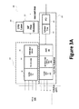
- FIG. 3A is a simplified diagram illustrating a communication interface 300 according to an embodiment of the present invention.
- FIG. 3B is a simplified diagram illustrating a segmented optical modulator according to an embodiment of the present invention.
- FIG. 4 is a simplified diagram illustrating a feedback mechanism according an embodiment of the invention.
- FIG. 5 is a simplified diagram illustrating the relationship between signal and noise according to an embodiment of the present invention.
- FIG. 6 is a simplified flow diagram illustrating a process for adjusting transmission power levels according to an embodiment of the present invention.
- the present invention is directed to data communication system and methods. More specifically, various embodiments of the present invention provide a communication interface that is configured to transfer data at high bandwidth using PAM format(s) over optical communication networks. A feedback mechanism is provided for adjusting the transmission power levels. There are other embodiments as well.
- Leaf-spine type of network architecture is provided to better allow servers to work in parallel and move data quickly among servers, offering high bandwidth and low latencies.
- a leaf-spine network architecture uses a top-of-rack switch that can directly access into server nodes and links back to a set of non-blocking spine switches that have enough bandwidth to allow for clusters of servers to be linked to one another and share large amount of data.
- any element in a claim that does not explicitly state “means for” performing a specified function, or “step for” performing a specific function, is not to be interpreted as a “means” or “step” clause as specified in 35 U.S.C. Section 112, Paragraph 6.
- the use of “step of” or “act of” in the Claims herein is not intended to invoke the provisions of 35, U.S.C. 112 Paragraph 6.
- FIG. 1 is a simplified diagram illustrating a leaf-spine architecture 100 according to an embodiment of the present invention.
- the leaf-spine architecture 100 comprises servers 120 , leaf switches 110 , and spine switches 103 . It is to be appreciated that depending on the need and specific application, the number and arrangement of the servers and switches may be changed. As shown in FIG. 1 , each server may be connected to more than one leaf switch. For example, server 121 is connected to leaf switches 111 and 112 . Similarly, server 122 is connected to leaf switches 111 and 112 , and so is server 123 .
- server 121 is connected to the leaf switch 111 via optical communication link utilizing pulse amplitude modulation (PAM).
- PAM2, PAM4, PAM8, PAM12, PAM16, and/or other variations of PAM may also be used in conjunction with optical communication links in various embodiments of the present invention.
- the bandwidth of the optical communication link between the server 121 and leaf switch 111 can be over 10 gigabits/s.
- Each leaf switch, such as leaf switch 111 may be connected to 10 or more servers. In one implementation, a leaf switch has a bandwidth of at least 100 gigabits/s.
- a leaf switch comprises a receiver device configured to receive four communication channels, and each of the channels is capable of transferring incoming data at 25 gigabits/s and configured as a PAM- 2 format.
- a server e.g. server 121
- the spine switches similarly, comprise communication interfaces for transmitting and receiving data in PAM format.
- the spine switches may have a large number of communication channels to accommodate a large number of leaf switches, each of which provides switching for a large number of servers.
- each leaf switch is connected to spine switches 101 and 102 .
- leaf switch 111 is connected to the spine switch 101 and 102 , and so are leaf switches 113 and 114 .
- each of the spine switches is configured with a bandwidth of 3.2 terabytes/s, which is big enough to communicate 32 optical communication links at 100 gigabits/s each. Depending on the specific implementation, other configuration and bandwidth are possible as well.
- the servers through the architecture 100 shown in FIG. 1 , can communicate with one another efficiently with a high bandwidth.
- Optical communication links are used between servers and leaf switches, and also between leaf switches and spine switches, and PAM utilized for optical network communication.
- FIG. 2 is a simplified diagram illustrating the form factor of a communication device according to an embodiment of the present invention.
- C form-factor pluggable (CFP) standard is widely adapted for gigabit network systems.
- Conventional electrical-connection based CFP transceivers often use 10 ⁇ 10 gigabits/s lines to achieve high bandwidth.
- CFP transceivers can utilize 10 ⁇ 10 gigabits/s configuration, 4 ⁇ 25 gigabits/s configuration, or others.
- a transceiver according to the present invention can have a much smaller form factor than CFP and CFP 2 as shown.
- communication interfaces according to the invention can have a form factor of CFP 4 or QSFP, which are much smaller in size than the CFP.
- the power consumption of communication interfaces according to the present invention can be much smaller.
- the power consumption can be as low as about 3W, which is about 1 ⁇ 4 that of convention transceivers with CFP form factor. The reduce level of power consumption helps save energy at data centers, where thousands (sometimes millions) of these communication devices are deployed.
- FIG. 3A is a simplified diagram illustrating a communication interface 300 according to an embodiment of the present invention. This diagram is merely an example, which should not unduly limit the scope of the claims. One of ordinary skill in the art would recognize many variations, alternatives, and modifications.
- the communication interface 300 includes transmitter module 310 and a receiver module 320 .
- the transmitter module 310 comprises a receiver 311 , encoder 312 , and PAM modulation driver 313 .
- the communication interface 300 is configured to receive incoming data at through four channels, where each channel is configured at 25 gigabits/s and configured as a PAM-2 format. Using the transmitter module 310 , modulator 316 , and the laser 314 , the communication interface 300 processes data received at 25 gigabits/s from each of the four incoming channels, and transmits PAM modulated optical data stream at a bandwidth of 100 gigabits/s. It is to be appreciated that other bandwidths are possible as well, such as 40 Gbps, 400 Gbps, and/or others.
- the transmitter module 310 receives 4 channels of data. It is to be appreciated that other variants of pulse-amplitude modulation (e.g., PAM4, PAM8, PAM12, PAM16, etc.), in addition to PAM-2 format, may be used as well.
- the transmitter module 310 comprises functional block 311 , which includes a clock data recovery (CDR) circuit configured to receive the incoming data from the four communication channels.
- the functional block 311 further comprises multiplexer for combining 4 channels for data.
- data from the 4 channels as shown are from the PCE-e interface 350 .
- the interface 350 is connected to one or more processors.
- two 2:1 multiplexers are employed in the functional block 311 .
- the data received from the four channels are high-speed data streams that are not accompanied by clock signals.
- the receiver 311 comprises, among other things, a clock signal that is associated with a predetermined frequency reference value.
- the receiver 311 is configured to utilize a phase-locked loop (PLL) to align the received data.
- PLL phase-locked loop
- the transmitter module 310 further comprises an encoder 312 .
- the encoder 312 comprises a forward error correction (FEC) encoder.
- FEC forward error correction
- the encoder 312 provides error detection and/or correction as needed.
- the data received is in a PAM- 2 format as described above.
- the received data comprises redundancy (e.g., one or more redundant bits) helps the encoder 312 to detect errors.
- redundancy e.g., one or more redundant bits
- LDPC low-density parity check
- the encoder 312 is configured to encode data received from four channels as shown to generate a data stream that can be transmitted through optical communication link at a bandwidth 100 gigabits/s (e.g., combining 4 channels of 25 gigabits/s data).
- each received is in the PAM-2 format
- the encoded data stream is a combination of four data channels and is in PAM-8 format.
- Data encoding and error correction are used under PAM format.
- the PAM formats as used in the embodiments of the present invention are further described below.
- the PAM modulation driver 313 is configured to drive data stream encoded by the encoder 312 .
- the receiver 311 , encoder 312 , and the modulation driver 313 are integrated and part of the transmitter module 310 .
- the PAM modulator 316 is configured to modulate signals from the transmitter module 310 , and convert the received electrical signal to optical signal using the laser 314 .
- the modulator 316 generates optical signals at a transmission rate of 100 gigabits per second. It is to be appreciated that other rate are possible as well, such as 40 Gbps, 400 Gbps, or others.
- the optical signals are transmitted in a PAM format (e.g., PAM-8 format, PAM12, PAM 16, etc.).
- the laser 314 comprises a distributed feedback (DFB) laser.
- DFB distributed feedback
- other types of laser technology may be used as well, as such vertical cavity surface emitting laser (VCSEL) and others.
- FIG. 3B is a simplified diagram illustrating a segmented optical modulator according to an embodiment of the present invention. This diagram is merely an example, which should not unduly limit the scope of the claims. One of ordinary skill in the art would recognize many variations, alternatives, and modifications. For example, modulated PAM signals modulated for transmission over optical communication links.
- the communication interface 300 is configured for both receiving and transmitting signals.
- a receiver module 320 comprise a photo detector 321 that converts incoming data signal in an optical format converts the optical signal to an electrical signal.
- the photo detector 321 comprises indium gallium arsenide material.
- the photo detector 321 can be a semiconductor-based photodiode, such as p-n photodiodes, p-i-n photodiodes, avalanche photodiodes, or others.
- the photo detector 321 is coupled with an amplifier 322 .
- the amplifier comprises a linear transimpedance amplifier (TIA).
- LRM long-range multi-mode
- the TIA helps compensate for optical dispersion in electrical domain using electrical dispersion compensation (EDC).
- EDC electrical dispersion compensation
- the amplifier 322 also includes a limiting amplifier. The amplifier 322 is used to produce a signal in the electrical domain from the incoming optical signal. In certain embodiments, further signal processing such as clock recovery from data (CDR) performed by a phase-locked loop may also be applied before the data is passed on.
- CDR clock recovery from data
- the amplified data signal from the amplifier 322 is processed by the analog to digital converter (ADC) 323 .
- the ADC 323 can be a baud rate ADC.
- the ADC is configured to convert the amplified signal into a digital signal formatted into a 100 gigabit per second signal in a PAM format.
- the functional block 324 is configured to process the 100 Gb/s data stream and encode it into four at streams at 25 Gb/s each.
- the incoming optical data stream received by the photo detector 321 is in PAM-8 format at a bandwidth of 100 Gb/s, and at block 324 four data streams in PAM-2 format is generated at a bandwidth of 25 Gb/s.
- the four data streams are transmitted by the transmitter 325 over 4 communication channels at 25 Gb/s.
- the communication interface 300 send optical signal to another communication interface. More specifically, the transmitter module of one network interface sends signals over optical network to the receiver module of another network interface.
- FIG. 4 is a simplified diagram illustrating a feedback mechanism according an embodiment of the invention. This diagram is merely an example, which should not unduly limit the scope of the claims. One of ordinary skill in the art would recognize many variations, alternatives, and modifications.
- the communication interface 410 is linked to and communicates with the communication interface 410 . For example, the communication interface 410 transmits data from its PAM modulator, through the optimal communication link 422 , and to the network interface 420 .
- the network interface 420 processes the signal received from the communication interface 410 , and based on the received signal, determines an optimal power level for communication between the two communication interfaces 410 and 420 .
- the network interface 420 sends, using its own PAM modulator and other components, the information regarding the optimal power level to the communication interface 410 via the optical communication link 421 .
- the network interface 420 comprises a processor units that processes the receive the signal to analysis the characteristics of optical transmission power and the noise thereof. For example, optical signal from the communication interface 410 is processed by the photodiode of the communication interface 420 and converted from optical signal to electrical signal. The characteristics of optical transmission power and the noise thereof are analyzed by the processor unit of the network interface 420 . The processor unit determines the optimal power level for data transmitted from network interface 410 through the optical communication 422 . The information related to the optimal power level is transmitted from encoded by the FEC encoder and transmitted through the PAM modulator of the network interface 420 to the network interface 410 via the optical communication link 421 . Detailed description for determining the optimal power level is described in more details below.
- the transmitter power levels are equispaced (i.e., spaced apart at equal distances) and the receiver threshold levels are set at the middle of two power levels.
- the receiver threshold level is set away from the midpoint.
- the noise is often signal dependent, which means that transmission power levels should not be equispaced.
- FIG. 5 is a simplified diagram illustrating the relationship between signal and noise according to an embodiment of the present invention. This diagram is merely an example, which should not unduly limit the scope of the claims. One of ordinary skill in the art would recognize many variations, alternatives, and modifications.
- the PAM optical communication interface 501 sends signals at M power levels, from P 1 to P M . Transmitted over optical communication link(s), signals is received by the communication interface 502 .
- the received signal is converted from optical signal to electrical signal by a photodiode, and then amplified by a TIA.
- the inputs received by the communication interface 502 comprise both signals V and noise M.
- the inputs at different power levels are V 1 +N 1 to V M +N M . It is to be appreciated that when transmitting signals over optical communication links, not only is power levels are selected, but the power levels are actually set. With the power levels that are set by the feedback system, the transmitter has optimized power levels to select from.
- FIG. 5 shows that the capacity achieving measures can be a function of the signal dependence of the noise. For example, it can be seen that distance between neighboring levels increases when the noise is more dependent on the signal and that the distance between the levels is smaller for lower signal levels. For example, the difference of power level between V M +N M and V M ⁇ 1 +N M ⁇ 1 is greater than the difference of power levels between V 2 +N 2 and V 1 +N 1 .
- a way of adjusting the power levels can be achieved at the receiver for a given set of receiver threshold levels. These transmission power levels can then be sent back to the transmitter. After the transmit level are changed, the receiver then re-adjusts it threshold levels and once again computes the optimal transmission power levels for this set of receiver parameters. In this way the feedback loop can be adjusted.
- the optimal receiver thresholds for a given set of transmitter levels and noise is given in the equations, which are provided below.
- a method for calculating the optimal transmitter power levels for a given set of receiver thresholds and noise is also provided.
- the noise has 3, components: (1) a signal independent component, (2) a component proportional to the signal power, and (3) a component proportional to the square of the signal power.
- the components of noise are attributed to the source or cause of noise, such as the present of short noise and laser intensity noise (RIN).
- the equations can be used to compute a gradient method of adjusting the receiver and transmitter parameters to optimize the system.
- receiver threshold levels T 1 to T M ⁇ 1 are set between input levels.
- the transmission levels P 1 and P M are set by the ratio of the transmitter and the maximum laser power available at the transmitter.
- a received input V k +N k has a signal component V k and noise component N k .
- the noise associated with the laser intensity noise is proportional to the square of the optical power.
- the shot noise ( ⁇ Sh,k ) is proportional to the optical power.
- the TIA noise is independent of the of the optical power. As modeled, these noise components are independent from one another, and the variance is added. For the purpose of modeling, these three components are assumed to be Gaussian.
- the probability of error P e , from the transmission can be calculated as:
- the optimal threshold values need to be determined. More specifically, for a given set of transmission power levels, P 1 , . . . , P m , the threshold levels T 1 , . . . , T M ⁇ 1 are to be determined, where the probably of error P e is minimized:
- the transmission power levels are adjusted to minimized the system probability of error, or P e .
- P e the system probability of error
- Equation 9 By substituting Equations 7 and 8 into Equation 6, Equation 9 below is obtained:
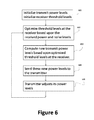
- FIG. 6 is a simplified flow diagram illustrating a process for adjusting transmission power levels according to an embodiment of the present invention. This diagram is merely an example, which should not unduly limit the scope of the claims.
- One of ordinary skill in the art would recognize many variations, alternatives, and modifications. For example, one or more steps may be added, removed, replaced, repeated, modified, rearranged, and/or repeated.
- the transmission power levels and threshold levels are initialized.
- network interfaces e.g., network interfaces 410 and 420
- the transmission power levels and threshold level may or may not be reset or initialized at each start up.
- threshold levels at the receiving network interface are optimized based on the received power and noise levels.
- the network interface 420 receives transmissions from the network interface 430 .
- the signal power level and the noise level are determined and used to optimize threshold levels, which are stored at the network interface 420 .
- the optimized threshold levels are determined by using equations explained above, which take, among other things, three noise components, into account.
- the receiving network interface computes new transmission power levels to be used by the transmitting network interface.
- the computation of transmission power levels is based at least on the threshold levels. For example, the relationship between the transmission power level and the threshold levels are described above.
- the receiving network interface (e.g., network interface 420 ) sends transmission power levels to the transmitting network interface (e.g., network interface 410 ).
- the transmission power level information is encoded and transmitted by the receiving network interface over optical communication links.
- the transmission power levels are received by the transmitting network interface, which adjusts its transmission power levels continues.
- the transmitting network interface 410 in FIG. 4 adjusts its transmission power levels using the transmission power level information received from the network interface 420 .
- the network interfaces that communicate with one another update the transmission power levels more than once during operation. More specifically, the receiving network interface continues to optimize threshold levels based on the signal and noise levels of the received transmissions. For example, the receiving network interface periodically updates the threshold level. In certain embodiments, the receiving network interface updates threshold level when a substantial change in transmission power and noise levels is detected. The update of threshold levels can be triggered by other events as well. For example, after step 605 , the processes loops back to step 602 so that the transmission levels can be adjusted and optimized as needed.
- the optimal power levels for data transmission can be determined, used, and updated, thereby allowing high data transmission rate and low error rate.
- Various embodiments of the present invention can be implemented with existing systems. For example, determination of power transmission levels and threshold levels can be performed by existing logic units and/or processors. There are other benefits as well.
Abstract
Description
Vk∝Pk,k=1, . . . , M
σNK 2=σTIA 2+σSh,k 2+σRINk 2
-
- Where: σRINk 2=βPk 2
- σSh,k 2=γPk
- σTIA 2=δ
- Where: σRINk 2=βPk 2
Claims (24)
Priority Applications (3)
| Application Number | Priority Date | Filing Date | Title |
|---|---|---|---|
| US14/599,833 US9467231B2 (en) | 2012-04-09 | 2015-01-19 | Method and system for transmitter optimization of an optical PAM serdes based on receiver feedback |
| US15/280,873 US9948396B2 (en) | 2012-04-09 | 2016-09-29 | Method and system for transmitter optimization of an optical PAM serdes based on receiver feedback |
| US15/917,382 US10333622B2 (en) | 2012-04-09 | 2018-03-09 | Method and system for transmitter optimization of an optical PAM serdes based on receiver feedback |
Applications Claiming Priority (6)
| Application Number | Priority Date | Filing Date | Title |
|---|---|---|---|
| US201261621920P | 2012-04-09 | 2012-04-09 | |
| US201261699724P | 2012-09-11 | 2012-09-11 | |
| US201261714543P | 2012-10-16 | 2012-10-16 | |
| US13/791,201 US9020346B2 (en) | 2012-09-11 | 2013-03-08 | Optical communication interface utilizing coded pulse amplitude modulation |
| US13/802,275 US9197324B1 (en) | 2012-04-09 | 2013-03-13 | Method and system for transmitter optimization of an optical PAM serdes based on receiver feedback |
| US14/599,833 US9467231B2 (en) | 2012-04-09 | 2015-01-19 | Method and system for transmitter optimization of an optical PAM serdes based on receiver feedback |
Related Parent Applications (1)
| Application Number | Title | Priority Date | Filing Date |
|---|---|---|---|
| US13/802,275 Continuation US9197324B1 (en) | 2012-04-09 | 2013-03-13 | Method and system for transmitter optimization of an optical PAM serdes based on receiver feedback |
Related Child Applications (1)
| Application Number | Title | Priority Date | Filing Date |
|---|---|---|---|
| US15/280,873 Continuation US9948396B2 (en) | 2012-04-09 | 2016-09-29 | Method and system for transmitter optimization of an optical PAM serdes based on receiver feedback |
Publications (2)
| Publication Number | Publication Date |
|---|---|
| US20150171963A1 US20150171963A1 (en) | 2015-06-18 |
| US9467231B2 true US9467231B2 (en) | 2016-10-11 |
Family
ID=53369774
Family Applications (4)
| Application Number | Title | Priority Date | Filing Date |
|---|---|---|---|
| US13/802,275 Active 2033-06-20 US9197324B1 (en) | 2012-04-09 | 2013-03-13 | Method and system for transmitter optimization of an optical PAM serdes based on receiver feedback |
| US14/599,833 Active 2033-03-28 US9467231B2 (en) | 2012-04-09 | 2015-01-19 | Method and system for transmitter optimization of an optical PAM serdes based on receiver feedback |
| US15/280,873 Active US9948396B2 (en) | 2012-04-09 | 2016-09-29 | Method and system for transmitter optimization of an optical PAM serdes based on receiver feedback |
| US15/917,382 Active US10333622B2 (en) | 2012-04-09 | 2018-03-09 | Method and system for transmitter optimization of an optical PAM serdes based on receiver feedback |
Family Applications Before (1)
| Application Number | Title | Priority Date | Filing Date |
|---|---|---|---|
| US13/802,275 Active 2033-06-20 US9197324B1 (en) | 2012-04-09 | 2013-03-13 | Method and system for transmitter optimization of an optical PAM serdes based on receiver feedback |
Family Applications After (2)
| Application Number | Title | Priority Date | Filing Date |
|---|---|---|---|
| US15/280,873 Active US9948396B2 (en) | 2012-04-09 | 2016-09-29 | Method and system for transmitter optimization of an optical PAM serdes based on receiver feedback |
| US15/917,382 Active US10333622B2 (en) | 2012-04-09 | 2018-03-09 | Method and system for transmitter optimization of an optical PAM serdes based on receiver feedback |
Country Status (1)
| Country | Link |
|---|---|
| US (4) | US9197324B1 (en) |
Cited By (3)
| Publication number | Priority date | Publication date | Assignee | Title |
|---|---|---|---|---|
| US20170019179A1 (en) * | 2012-04-09 | 2017-01-19 | Inphi Corporation | Method and system for transmitter optimization of an optical pam serdes based on receiver feedback |
| WO2021094790A1 (en) | 2019-11-14 | 2021-05-20 | Mellanox Technologies Ltd | Voltage controlled electro-optical serializer/deserializer (serdes) |
| US11791903B2 (en) | 2019-05-13 | 2023-10-17 | Mellanox Technologies, Ltd. | Consolidating multiple electrical data signals into an optical data signal on a multi-chip module using ASIC for controlling a photonics transceiver |
Families Citing this family (35)
| Publication number | Priority date | Publication date | Assignee | Title |
|---|---|---|---|---|
| US9430437B1 (en) * | 2013-08-09 | 2016-08-30 | Inphi Corporation | PCIE lane aggregation over a high speed link |
| EP3417553A1 (en) * | 2016-02-19 | 2018-12-26 | BAE Systems PLC | Optical sensing and communications system |
| US9559880B1 (en) * | 2016-03-04 | 2017-01-31 | Inphi Corporation | Eye modulation for pulse-amplitude modulation communication systems |
| CN107087059B (en) * | 2017-03-30 | 2020-09-29 | 努比亚技术有限公司 | Data transmission system and method |
| CN107087063B (en) * | 2017-03-30 | 2020-11-03 | 易网数字物流(宁波)有限公司 | Data transmission system and method |
| EP3639412B1 (en) * | 2017-06-27 | 2022-01-26 | Huawei Technologies Co., Ltd. | Pulse amplitude modulation level optimization and equalization in optical systems |
| US10212010B2 (en) * | 2017-07-13 | 2019-02-19 | Zte Corporation | Unequally spaced pulse amplitude modulation scheme |
| KR102017879B1 (en) | 2017-11-23 | 2019-10-21 | 한국전자통신연구원 | An optical signal transmitting apparatus generating an optical signal having multple levles and a method performed by the optical signal transmitting appratus |
| KR102433875B1 (en) * | 2018-03-23 | 2022-08-19 | 삼성전자주식회사 | Display apparatus and controlling method of the display apparatus |
| US11239919B2 (en) * | 2018-12-20 | 2022-02-01 | Acacia Communications, Inc. | Side channel communication for an optical coherent transceiver |
| EP3917033A4 (en) * | 2019-03-25 | 2022-04-06 | NEC Corporation | Optical transfer system, optical transmitter, and optical communication method |
| US11018776B2 (en) | 2019-04-18 | 2021-05-25 | Microsoft Technology Licensing, Llc | Power-based decoding of data received over an optical communication path |
| US10756817B1 (en) | 2019-04-18 | 2020-08-25 | Microsoft Technology Licensing, Llc | Power switching for systems implementing throughput improvements for optical communications |
| US10742325B1 (en) | 2019-04-18 | 2020-08-11 | Microsoft Technology Licensing, Llc | Power-based encoding of data to be transmitted over an optical communication path |
| US10862591B1 (en) | 2019-04-18 | 2020-12-08 | Microsoft Technology Licensing, Llc | Unequal decision regions for throughput increases for optical communications |
| US10742326B1 (en) | 2019-04-18 | 2020-08-11 | Microsoft Technology Licensing, Llc | Power-based encoding of data to be transmitted over an optical communication path |
| US10998982B2 (en) | 2019-04-18 | 2021-05-04 | Microsoft Technology Licensing, Llc | Transmitter for throughput increases for optical communications |
| US10892847B2 (en) | 2019-04-18 | 2021-01-12 | Microsoft Technology Licensing, Llc | Blind detection model optimization |
| US10897315B2 (en) | 2019-04-18 | 2021-01-19 | Microsoft Technology Licensing, Llc | Power-based decoding of data received over an optical communication path |
| US10938485B2 (en) | 2019-04-18 | 2021-03-02 | Microsoft Technology Licensing, Llc | Error control coding with dynamic ranges |
| US10911155B2 (en) | 2019-04-18 | 2021-02-02 | Microsoft Technology Licensing, Llc | System for throughput increases for optical communications |
| US10873393B2 (en) * | 2019-04-18 | 2020-12-22 | Microsoft Technology Licensing, Llc | Receiver training for throughput increases in optical communications |
| US10911152B2 (en) | 2019-04-18 | 2021-02-02 | Microsoft Technology Licensing, Llc | Power-based decoding of data received over an optical communication path |
| US10951342B2 (en) | 2019-04-18 | 2021-03-16 | Microsoft Technology Licensing, Llc | Throughput increases for optical communications |
| US10873392B2 (en) | 2019-04-18 | 2020-12-22 | Microsoft Technology Licensing, Llc | Throughput increases for optical communications |
| US11063696B2 (en) | 2019-07-16 | 2021-07-13 | Microsoft Technology Licensing, Llc | Increasing average power levels to reduce peak-to-average power levels using error correction codes |
| US11031961B2 (en) | 2019-07-16 | 2021-06-08 | Microsoft Technology Licensing, Llc | Smart symbol changes for optimization of communications using error correction |
| US11075656B2 (en) | 2019-07-16 | 2021-07-27 | Microsoft Technology Licensing, Llc | Bit error reduction of communication systems using error correction |
| US11172455B2 (en) | 2019-07-16 | 2021-11-09 | Microsoft Technology Licensing, Llc | Peak to average power output reduction of RF systems utilizing error correction |
| US11086719B2 (en) | 2019-07-16 | 2021-08-10 | Microsoft Technology Licensing, Llc | Use of error correction codes to prevent errors in neighboring storage |
| US11044044B2 (en) * | 2019-07-16 | 2021-06-22 | Microsoft Technology Licensing, Llc | Peak to average power ratio reduction of optical systems utilizing error correction |
| US10911141B1 (en) | 2019-07-30 | 2021-02-02 | Microsoft Technology Licensing, Llc | Dynamically selecting a channel model for optical communications |
| JP2022143378A (en) * | 2021-03-17 | 2022-10-03 | 富士通オプティカルコンポーネンツ株式会社 | Control apparatus of modulation signal |
| US11536916B1 (en) * | 2021-05-10 | 2022-12-27 | Amazon Technologies, Inc. | Pathloss optimization for optical systems |
| JP2023003580A (en) * | 2021-06-24 | 2023-01-17 | 住友電工デバイス・イノベーション株式会社 | Communication system, optical transceiver, control method for communication system and control method for optical transceiver |
Citations (22)
| Publication number | Priority date | Publication date | Assignee | Title |
|---|---|---|---|---|
| US20020166091A1 (en) * | 2000-06-05 | 2002-11-07 | Kidorf Howard D. | Concatenated forward error correction decoder |
| US20030223762A1 (en) * | 2001-05-14 | 2003-12-04 | Keangpo Ho | Multilevel optical signals optimized for systems having signal-dependent and signal-independent noises, finite transmitter extinction ratio and intersymbol interference |
| US20040037569A1 (en) * | 2002-08-22 | 2004-02-26 | Kamalov Valey F. | Method and device for evaluating and improving the quality of transmission of a telecommunications signal through an optical fiber |
| US6826372B1 (en) * | 2000-08-30 | 2004-11-30 | Sycamore Networks, Inc. | Methods and apparatus for dynamic threshold setting for an optically amplified receiver |
| US20050123295A1 (en) * | 2003-12-04 | 2005-06-09 | Alcatel | Transmission system and method for equalization of channels in the system |
| US7113708B1 (en) * | 1998-11-17 | 2006-09-26 | Barr & Stroud Limited | Data communications link |
| US20080069570A1 (en) * | 2006-09-15 | 2008-03-20 | John Dallesasse | Optical transceiver for 100 Gigabit/second transmission |
| US7389046B1 (en) * | 2005-01-18 | 2008-06-17 | Woven Systems, Inc. | Simplified switching interconnect using wavelength division multiplexing |
| US20090154500A1 (en) * | 2007-12-17 | 2009-06-18 | Wael William Diab | Method And System For Energy Efficient Signaling For 100MBPS Ethernet Using A Subset Technique |
| US20090269055A1 (en) * | 2008-04-23 | 2009-10-29 | Alcatel Lucent | Channel balancing algorithm |
| US20090297148A1 (en) * | 2008-05-27 | 2009-12-03 | Xtera Communications Ltd. | Automatic pre-emphasis |
| US20100008662A1 (en) * | 2008-07-14 | 2010-01-14 | Bradbeer Peter F | Method and system for closed loop control of an optical link |
| US7734191B1 (en) * | 2002-10-08 | 2010-06-08 | Infinera Corporation | Forward error correction (FEC) enabled photonic integrated circuit (PICs) chips with multiple signal channels |
| US20100254703A1 (en) * | 2009-04-01 | 2010-10-07 | Kirkpatrick Peter E | Optical Network for Cluster Computing |
| US7941053B2 (en) * | 2006-10-19 | 2011-05-10 | Emcore Corporation | Optical transceiver for 40 gigabit/second transmission |
| US20110236017A1 (en) * | 2008-12-01 | 2011-09-29 | Peter Ohlen | Methods and Devices for Wavelength Alignment in WDM-PON |
| US20110236028A1 (en) * | 2010-03-24 | 2011-09-29 | Avago Technologies Fiber Ip (Singapore) Pte. Ltd. | Method and apparatus for compensating for optical crosstalk in an optical output power feedback monitoring system of a parallel optical transmitter |
| US8103137B2 (en) * | 2009-04-01 | 2012-01-24 | Fusion-Io, Inc. | Optical network for cluster computing |
| US20130004161A1 (en) * | 2010-03-12 | 2013-01-03 | Zte Corporation | Optical power adjustment method for ethernet passive optical network system, and optical line terminal |
| US8406128B1 (en) * | 2010-06-29 | 2013-03-26 | Amazon Technologies, Inc. | Efficient highly connected data centers |
| US20130156425A1 (en) * | 2011-12-17 | 2013-06-20 | Peter E. Kirkpatrick | Optical Network for Cluster Computing |
| US9197324B1 (en) * | 2012-04-09 | 2015-11-24 | Inphi Corporation | Method and system for transmitter optimization of an optical PAM serdes based on receiver feedback |
Family Cites Families (14)
| Publication number | Priority date | Publication date | Assignee | Title |
|---|---|---|---|---|
| GB2367912B (en) | 2000-08-08 | 2003-01-08 | Sun Microsystems Inc | Apparatus for testing computer memory |
| GB2366925A (en) * | 2000-09-13 | 2002-03-20 | Marconi Comm Ltd | Power control and equalisation in an optical WDM system |
| JP3837704B2 (en) * | 2002-02-07 | 2006-10-25 | 富士通株式会社 | Optical multiplex communication system, optical transmitter, and optical multiplex communication control method |
| JP4010877B2 (en) * | 2002-06-03 | 2007-11-21 | 富士通株式会社 | Optical transmission system |
| US7756421B2 (en) * | 2002-10-03 | 2010-07-13 | Ciena Corporation | Electrical domain compensation of non-linear effects in an optical communications system |
| US20060294443A1 (en) | 2005-06-03 | 2006-12-28 | Khaled Fekih-Romdhane | On-chip address generation |
| JP4571054B2 (en) * | 2005-09-30 | 2010-10-27 | 富士通株式会社 | Optical wavelength control method and system |
| EP2020767B1 (en) * | 2006-05-25 | 2017-08-02 | Mitsubishi Electric Corporation | Optical relay device and optical relay transmission system |
| US8086110B2 (en) * | 2007-03-14 | 2011-12-27 | Intel Corporation | Optical wavelength division multiplexing (WDM) system including adaptive cross-talk cancellation |
| US20090245114A1 (en) | 2008-04-01 | 2009-10-01 | Jayanth Vijayaraghavan | Methods for collecting and analyzing network performance data |
| US8731401B2 (en) | 2010-12-14 | 2014-05-20 | University Of Houston | Dense wavelength division multiplexing multi-mode switching systems and methods for concurrent and dynamic reconfiguration with different switching modes |
| JP5564692B2 (en) * | 2011-02-25 | 2014-07-30 | 株式会社日立製作所 | Optical transmission system and optical node |
| US20120250679A1 (en) | 2011-03-29 | 2012-10-04 | Amazon Technologies, Inc. | Network Transpose Box and Switch Operation Based on Backplane Ethernet |
| US8903205B2 (en) * | 2012-02-23 | 2014-12-02 | Karlsruhe Institute of Technology (KIT) | Three-dimensional freeform waveguides for chip-chip connections |
-
2013
- 2013-03-13 US US13/802,275 patent/US9197324B1/en active Active
-
2015
- 2015-01-19 US US14/599,833 patent/US9467231B2/en active Active
-
2016
- 2016-09-29 US US15/280,873 patent/US9948396B2/en active Active
-
2018
- 2018-03-09 US US15/917,382 patent/US10333622B2/en active Active
Patent Citations (22)
| Publication number | Priority date | Publication date | Assignee | Title |
|---|---|---|---|---|
| US7113708B1 (en) * | 1998-11-17 | 2006-09-26 | Barr & Stroud Limited | Data communications link |
| US20020166091A1 (en) * | 2000-06-05 | 2002-11-07 | Kidorf Howard D. | Concatenated forward error correction decoder |
| US6826372B1 (en) * | 2000-08-30 | 2004-11-30 | Sycamore Networks, Inc. | Methods and apparatus for dynamic threshold setting for an optically amplified receiver |
| US20030223762A1 (en) * | 2001-05-14 | 2003-12-04 | Keangpo Ho | Multilevel optical signals optimized for systems having signal-dependent and signal-independent noises, finite transmitter extinction ratio and intersymbol interference |
| US20040037569A1 (en) * | 2002-08-22 | 2004-02-26 | Kamalov Valey F. | Method and device for evaluating and improving the quality of transmission of a telecommunications signal through an optical fiber |
| US7734191B1 (en) * | 2002-10-08 | 2010-06-08 | Infinera Corporation | Forward error correction (FEC) enabled photonic integrated circuit (PICs) chips with multiple signal channels |
| US20050123295A1 (en) * | 2003-12-04 | 2005-06-09 | Alcatel | Transmission system and method for equalization of channels in the system |
| US7389046B1 (en) * | 2005-01-18 | 2008-06-17 | Woven Systems, Inc. | Simplified switching interconnect using wavelength division multiplexing |
| US20080069570A1 (en) * | 2006-09-15 | 2008-03-20 | John Dallesasse | Optical transceiver for 100 Gigabit/second transmission |
| US7941053B2 (en) * | 2006-10-19 | 2011-05-10 | Emcore Corporation | Optical transceiver for 40 gigabit/second transmission |
| US20090154500A1 (en) * | 2007-12-17 | 2009-06-18 | Wael William Diab | Method And System For Energy Efficient Signaling For 100MBPS Ethernet Using A Subset Technique |
| US20090269055A1 (en) * | 2008-04-23 | 2009-10-29 | Alcatel Lucent | Channel balancing algorithm |
| US20090297148A1 (en) * | 2008-05-27 | 2009-12-03 | Xtera Communications Ltd. | Automatic pre-emphasis |
| US20100008662A1 (en) * | 2008-07-14 | 2010-01-14 | Bradbeer Peter F | Method and system for closed loop control of an optical link |
| US20110236017A1 (en) * | 2008-12-01 | 2011-09-29 | Peter Ohlen | Methods and Devices for Wavelength Alignment in WDM-PON |
| US20100254703A1 (en) * | 2009-04-01 | 2010-10-07 | Kirkpatrick Peter E | Optical Network for Cluster Computing |
| US8103137B2 (en) * | 2009-04-01 | 2012-01-24 | Fusion-Io, Inc. | Optical network for cluster computing |
| US20130004161A1 (en) * | 2010-03-12 | 2013-01-03 | Zte Corporation | Optical power adjustment method for ethernet passive optical network system, and optical line terminal |
| US20110236028A1 (en) * | 2010-03-24 | 2011-09-29 | Avago Technologies Fiber Ip (Singapore) Pte. Ltd. | Method and apparatus for compensating for optical crosstalk in an optical output power feedback monitoring system of a parallel optical transmitter |
| US8406128B1 (en) * | 2010-06-29 | 2013-03-26 | Amazon Technologies, Inc. | Efficient highly connected data centers |
| US20130156425A1 (en) * | 2011-12-17 | 2013-06-20 | Peter E. Kirkpatrick | Optical Network for Cluster Computing |
| US9197324B1 (en) * | 2012-04-09 | 2015-11-24 | Inphi Corporation | Method and system for transmitter optimization of an optical PAM serdes based on receiver feedback |
Cited By (5)
| Publication number | Priority date | Publication date | Assignee | Title |
|---|---|---|---|---|
| US20170019179A1 (en) * | 2012-04-09 | 2017-01-19 | Inphi Corporation | Method and system for transmitter optimization of an optical pam serdes based on receiver feedback |
| US9948396B2 (en) * | 2012-04-09 | 2018-04-17 | Inphi Corporation | Method and system for transmitter optimization of an optical PAM serdes based on receiver feedback |
| US11791903B2 (en) | 2019-05-13 | 2023-10-17 | Mellanox Technologies, Ltd. | Consolidating multiple electrical data signals into an optical data signal on a multi-chip module using ASIC for controlling a photonics transceiver |
| WO2021094790A1 (en) | 2019-11-14 | 2021-05-20 | Mellanox Technologies Ltd | Voltage controlled electro-optical serializer/deserializer (serdes) |
| US11750297B2 (en) | 2019-11-14 | 2023-09-05 | Mellanox Technologies, Ltd. | Voltage controlled electro-optical serializer/deserializer (SerDes) |
Also Published As
| Publication number | Publication date |
|---|---|
| US20150171963A1 (en) | 2015-06-18 |
| US10333622B2 (en) | 2019-06-25 |
| US9197324B1 (en) | 2015-11-24 |
| US20180198527A1 (en) | 2018-07-12 |
| US9948396B2 (en) | 2018-04-17 |
| US20170019179A1 (en) | 2017-01-19 |
Similar Documents
| Publication | Publication Date | Title |
|---|---|---|
| US10333622B2 (en) | Method and system for transmitter optimization of an optical PAM serdes based on receiver feedback | |
| US11451300B2 (en) | Optical communication interface utilizing n-dimensional double square quadrature amplitude modulation | |
| US10148361B2 (en) | Optical PAM modulation with dual drive Mach Zehnder modulators and low complexity electrical signaling | |
| US9020346B2 (en) | Optical communication interface utilizing coded pulse amplitude modulation | |
| US10355886B2 (en) | FEC coding identification | |
| US9488896B2 (en) | Direct-coupled driver for Mach-Zehnder optical modulators | |
| US10649951B2 (en) | Monolithically integrated system on chip for silicon photonics | |
| US20170318363A1 (en) | Multilane variable bias for an optical modulator | |
| US20170359636A1 (en) | Configurable multi-rate format for communication system for silicon photonics | |
| CN105122688B (en) | Use the optical communication interface of quadrature amplitude modulation | |
| US9621280B2 (en) | Built-in redundancy scheme for communication system on chip |
Legal Events
| Date | Code | Title | Description |
|---|---|---|---|
| STCF | Information on status: patent grant |
Free format text: PATENTED CASE |
|
| FEPP | Fee payment procedure |
Free format text: PAYOR NUMBER ASSIGNED (ORIGINAL EVENT CODE: ASPN); ENTITY STATUS OF PATENT OWNER: LARGE ENTITY |
|
| AS | Assignment |
Owner name: INPHI CORPORATION, CALIFORNIA Free format text: ASSIGNMENT OF ASSIGNORS INTEREST;ASSIGNORS:BHOJA, SUDEEP;XU, CHAO;SHANKAR, HARI;SIGNING DATES FROM 20130411 TO 20130524;REEL/FRAME:041886/0534 |
|
| FEPP | Fee payment procedure |
Free format text: ENTITY STATUS SET TO UNDISCOUNTED (ORIGINAL EVENT CODE: BIG.) |
|
| MAFP | Maintenance fee payment |
Free format text: PAYMENT OF MAINTENANCE FEE, 4TH YEAR, LARGE ENTITY (ORIGINAL EVENT CODE: M1551); ENTITY STATUS OF PATENT OWNER: LARGE ENTITY Year of fee payment: 4 |
|
| AS | Assignment |
Owner name: MARVELL TECHNOLOGY CAYMAN I, CAYMAN ISLANDS Free format text: ASSIGNMENT OF ASSIGNORS INTEREST;ASSIGNOR:INPHI CORPORATION;REEL/FRAME:056649/0823 Effective date: 20210617 |
|
| AS | Assignment |
Owner name: CAVIUM INTERNATIONAL, CAYMAN ISLANDS Free format text: ASSIGNMENT OF ASSIGNORS INTEREST;ASSIGNOR:MARVELL TECHNOLOGY CAYMAN I;REEL/FRAME:057279/0519 Effective date: 20210620 |
|
| AS | Assignment |
Owner name: MARVELL ASIA PTE LTD., SINGAPORE Free format text: ASSIGNMENT OF ASSIGNORS INTEREST;ASSIGNOR:CAVIUM INTERNATIONAL;REEL/FRAME:057336/0873 Effective date: 20210620 |