US9484948B2 - Clock generation circuit - Google Patents
Clock generation circuit Download PDFInfo
- Publication number
- US9484948B2 US9484948B2 US14/539,293 US201414539293A US9484948B2 US 9484948 B2 US9484948 B2 US 9484948B2 US 201414539293 A US201414539293 A US 201414539293A US 9484948 B2 US9484948 B2 US 9484948B2
- Authority
- US
- United States
- Prior art keywords
- clock signal
- signal
- phase difference
- frequency
- output
- Prior art date
- Legal status (The legal status is an assumption and is not a legal conclusion. Google has not performed a legal analysis and makes no representation as to the accuracy of the status listed.)
- Active, expires
Links
Images


Classifications
-
- H—ELECTRICITY
- H03—ELECTRONIC CIRCUITRY
- H03M—CODING; DECODING; CODE CONVERSION IN GENERAL
- H03M3/00—Conversion of analogue values to or from differential modulation
- H03M3/30—Delta-sigma modulation
-
- H—ELECTRICITY
- H03—ELECTRONIC CIRCUITRY
- H03K—PULSE TECHNIQUE
- H03K21/00—Details of pulse counters or frequency dividers
- H03K21/02—Input circuits
-
- H—ELECTRICITY
- H03—ELECTRONIC CIRCUITRY
- H03K—PULSE TECHNIQUE
- H03K21/00—Details of pulse counters or frequency dividers
- H03K21/02—Input circuits
- H03K21/023—Input circuits comprising pulse shaping or differentiating circuits
-
- H—ELECTRICITY
- H03—ELECTRONIC CIRCUITRY
- H03L—AUTOMATIC CONTROL, STARTING, SYNCHRONISATION, OR STABILISATION OF GENERATORS OF ELECTRONIC OSCILLATIONS OR PULSES
- H03L7/00—Automatic control of frequency or phase; Synchronisation
- H03L7/06—Automatic control of frequency or phase; Synchronisation using a reference signal applied to a frequency- or phase-locked loop
- H03L7/16—Indirect frequency synthesis, i.e. generating a desired one of a number of predetermined frequencies using a frequency- or phase-locked loop
- H03L7/18—Indirect frequency synthesis, i.e. generating a desired one of a number of predetermined frequencies using a frequency- or phase-locked loop using a frequency divider or counter in the loop
- H03L7/197—Indirect frequency synthesis, i.e. generating a desired one of a number of predetermined frequencies using a frequency- or phase-locked loop using a frequency divider or counter in the loop a time difference being used for locking the loop, the counter counting between numbers which are variable in time or the frequency divider dividing by a factor variable in time, e.g. for obtaining fractional frequency division
Definitions
- the present technique relates to a clock generation circuit. More particularly, the present technique relates to a clock generation circuit for multiplying a frequency of a clock signal and outputting the signal.
- a clock generation circuit having an NCO (Numerical Controlled Oscillator), a loop filter, and a DLL (Delay Locked Loop) has been suggested (for example, see PTL 1).
- NCO Numerical Controlled Oscillator
- loop filter a loop filter
- DLL Delay Locked Loop
- This clock generation circuit outputs an overflow signal by changing the count value of the NCO on the basis of phase information.
- this overflow signal as a clock signal, a clock signal of any given average frequency can be attained.
- the amount of jitter is reduced in the overflow signal given by the NCO by further increasing the time precision with a DLL in a later stage.
- a loop filter can be constituted by a digital circuit for a low frequency reference clock signal, and therefore, as compared with the case where an analog filter is used, the loop band can be reduced with a smaller size of implementation area.
- periodical jitter component remains in the clock signal generated by the NCO and the DLL.
- a PLL Phase Locked Loop
- a jitter having a higher frequency component than the loop band of the PLL can be suppressed.
- a clock signal still including a jitter of a low frequency component generated by the NCO and the DLL are output.
- the clock generation circuit may not sufficiently reduce the noise in the clock signal which is output.
- the present technique is made in view of such circumstances, and the present inventors have recognized that the present technique to reduce the noise in the clock signal.
- the present technique is made to solve the above problems, and the first aspect is a clock generation circuit including a phase difference comparison circuit configured to compare a phase of each of an input clock signal and a feedback signal which have been input, and provides a phase difference signal indicating a phase difference between the input clock signal and the feedback signal, a filter circuit configured to suppress a high frequency component, of which frequency is higher than a predetermined cutoff frequency, in the phase difference signal, an output circuit configured to modulate the phase difference signal, of which high frequency component is suppressed, in such a manner as to decrease a noise component of a low frequency band and increase a noise component of a high frequency band, and generate and output an output clock signal from the modulated phase difference signal and a reference clock signal, and a frequency dividing circuit configured to divide a frequency of the output clock signal, which has been output, at a predetermined frequency dividing ratio, and feed the output clock signal back to the phase comparison circuit as the feedback signal. Therefore, there is an advantage in that the output clock signal is generated from the modulated phase difference signal
- the output circuit may include a modulator configured to modulate the phase difference signal of which high frequency component has been suppressed, and a multiplier circuit configured to multiply the reference clock signal by a multiplication ratio according to the phase difference indicated by the frequency dividing ratio setting signal which has been modulated, and output the output clock signal. Therefore, there is an advantage in that the reference clock signal is multiplied by the multiplication ratio according to the phase difference.
- the output circuit may further include an adjustment unit configured to adjust the phase difference indicated by the phase difference signal so that it attains a value obtained by multiplying a ratio of a frequency of the reference clock signal with respect to a frequency of the input clock signal by the predetermined frequency dividing ratio, and input the phase difference signal indicating the adjusted value into the modulator. Therefore, there is an advantage in that the phase difference is adjusted to attain the value obtained by multiplying the ratio of the frequency of the reference clock signal with respect to the frequency of the input clock signal by the predetermined frequency dividing ratio.
- the multiplier circuit may include a phase difference detector configured to compare phases of the reference clock signal and an internal signal, and detect a phase difference between the reference clock signal and the internal signal, an oscillator configured to oscillate at a frequency according to the phase difference detected by the phase difference detector, and generate the output clock signal, and a variable frequency divider configured to divide a frequency of the output clock signal, which has been generated, at a frequency dividing ratio equal to the value indicated by the phase difference signal which has been modulated, and feed the output clock signal back to the phase difference detector as the internal signal. Therefore, there is an advantage in that the frequency of the output clock signal is divided by the frequency dividing ratio equal to the value indicated by the phase difference signal.
- the clock generation circuit may further include a detection circuit configured to provide the phase comparison circuit with a detection result obtained by detecting an edge of the input clock signal on the basis of a clock signal of a frequency higher than the input clock signal. Therefore, there is an advantage in that the edge of the input clock signal is detected on the basis of the clock signal of a frequency higher than the input clock signal.
- the detection circuit may detect an edge of the input clock signal on the basis of the output clock signal. Therefore, there is an advantage in that the edge of the input clock signal is detected on the basis of the output clock signal.
- the modulation performed on the phase difference signal may be sigma delta modulation. Therefore, there is an advantage in that the sigma delta modulation is performed on the phase difference signal.
- the second aspect of the present technique is an electronic device including a reference clock providing circuit configured to provide a predetermined reference clock signal, a phase difference comparison circuit configured to compare a phase of each of an input clock signal and a feedback signal which have been input, and provides a phase difference signal indicating a phase difference between the input clock signal and the feedback signal, a filter circuit configured to suppress a high frequency component, of which frequency is higher than a predetermined cutoff frequency, in the phase difference signal, an output circuit configured to modulate the phase difference signal, of which high frequency component is suppressed, in such a manner as to decrease a noise component of a low frequency band and increase a noise component of a high frequency band, and generate and output an output clock signal from the modulated phase difference signal and a reference clock signal, and a frequency dividing circuit configured to divide a frequency of the output clock signal, which
- the present technique achieves a superior effect of reducing noises in a clock signal. It should be noted that the advantages described here is not particularly limited, and any one of the advantages described in the present disclosure may be achieved.
- FIG. 1 is a block diagram illustrating an example of configuration of an electronic device according to a first embodiment.
- FIG. 2 is a block diagram illustrating an example of configuration of a clock generation circuit according to the first embodiment.
- FIG. 4 is a block diagram illustrating an example of configuration of an electronic device according to a first modification of the first embodiment.
- FIG. 5 is a block diagram illustrating an example of configuration of an electronic device according to a second modification of the first embodiment.
- FIG. 6 is a block diagram illustrating an example of configuration of a clock generation circuit according to a third modification of the first embodiment.
- FIG. 8 is a block diagram illustrating an example of configuration of a clock generation circuit according to a second embodiment.
- FIG. 9 is a block diagram illustrating an example of configuration of a clock generation circuit according to a modification of the second embodiment.
- FIG. 1 is a block diagram illustrating an example of configuration of an electronic device 100 according to the first embodiment.
- This electronic device 100 includes an AD (Analog-to-Digital) conversion circuit 110 , a logic circuit 120 , and a clock generation circuit 200 .
- AD Analog-to-Digital
- the clock generation circuit 200 generates an output clock signal CLKOUT from an input clock signal CLKIN and a reference clock signal bCLK.
- the input clock signal CLKIN is, for example, a horizontal synchronization signal, and is transmitted from the source of a video player and the like to the clock generation circuit 200 .
- the reference clock signal bCLK is a clock signal of which frequency is constant, and is, for example, provided from a crystal oscillator CXO to the clock generation circuit 200 .
- the frequency of the input clock signal CLKIN is, for example, 10 kHz
- the frequency of the reference clock signal bCLK is, for example, 48 MHz.
- the crystal oscillator CXO is provided outside of the electronic device 100 , the crystal oscillator CXO may be provided inside of the electronic device 100 .
- the crystal oscillator CXO is an example of a reference clock providing circuit as described in the claims.
- the clock generation circuit 200 uses the reference clock signal bCLK to generate the output clock signal CLKOUT by multiplying the frequency of the input clock signal CLKIN, and provides it to the AD conversion circuit 110 and logic circuit 120 .
- the details of the generation method of the output clock signal CLKOUT will be explained later.
- the AD conversion circuit 110 converts the analog signal into a digital signal in synchronization with the output clock signal CLKOUT.
- the analog signal is a video signal, an audio signal, and the like, and is transmitted from a source to the AD conversion circuit 110 .
- the AD conversion circuit 110 provides the digital signal to the logic circuit 120 .
- the logic circuit 120 performs predetermined processing on the digital signal in synchronization with the output clock signal CLKOUT. For example, image processing, decoding processing, noise reduction processing, and the like are performed on the digital signal.
- the logic circuit 120 provides the processed digital signal to a sink such as a display device.
- FIG. 2 is a block diagram illustrating an example of configuration of the clock generation circuit 200 according to the first embodiment.
- This clock generation circuit 200 includes a phase comparison circuit 210 , a digital filter 220 , a non-integral multiplier phase synchronization circuit 230 , and a feedback frequency divider circuit 250 .
- the phase comparison circuit 210 detects the phase difference by comparing the phases of the input clock signal CLKIN and the feedback signal fbCLK 1 .
- the phase comparison circuit 210 generates a phase difference signal DIF 1 indicating the detected phase difference, and provides it to the digital filter 220 .
- the digital filter 220 suppresses a high frequency component than a predetermined cutoff frequency in the phase difference signal DIF 1 .
- This digital filter 220 may be, for example, an IIR (Infinite Impulse Response) filter and an FIR (Finite Impulse Response) filter.
- the operation clock of the digital filter 220 may be, for example, the reference clock signal bCLK given by the crystal oscillator CXO.
- the digital filter 220 provides the phase difference signal DIF 1 , of which high frequency component is suppressed, to the non-integral multiplier phase synchronization circuit 230 .
- the digital filter 220 is an example of a filter circuit as described in the claims.
- the use of the digital filter 220 can reduce the increase in the size of area of the filter even if the frequency of the reference clock signal bCLK is low. In addition, this makes it unnecessary to have components be provided outside of the LSI (Large Scale Integration). Still more, the digital filter 220 is a combination of logic circuits, and therefore, with the progress in the technique of LSI manufacturing process, the digital filter 220 can be made into a smaller size, consume less power, and increase the speed.
- An analog filter may be used instead of the digital filter 220 , as long as the high frequency component can be suppressed in the phase difference signal DIF 1 .
- the non-integral multiplier phase synchronization circuit 230 performs sigma delta modulation on the phase difference signal DIF 1 of which high frequency component has been suppressed.
- This non-integral multiplier phase synchronization circuit 230 generates the output clock signal CLKOUT from the reference clock signal bCLK and the phase difference signal DIF 1 on which the sigma delta modulation has been performed, and provides the output clock signal CLKOUT to the AD conversion circuit 110 , the logic circuit 120 , and the feedback frequency divider circuit 250 .
- the non-integral multiplier phase synchronization circuit 230 is an example of an output circuit as described in the claims.
- the feedback frequency divider circuit 250 divides the frequency of the output clock signal CLKOUT with a predetermined frequency dividing ratio, and feeds it back to the phase comparison circuit 210 as a feedback signal fbCLK 1 .
- the feedback frequency divider circuit 250 is constituted by, for example, a counter circuit and the like.
- the frequency dividing ratio is set to, for example, 160 ⁇ 10 3 . Therefore, when the frequency of the input clock signal CLKIN is 10 kHz, an output clock signal CLKOUT of 160 MHz is generated.
- the feedback frequency divider circuit 250 is an example of a frequency dividing circuit as described in the claims.
- FIG. 3 is a block diagram illustrating an example of configuration of the non-integral multiplier phase synchronization circuit 230 according to the first embodiment.
- This non-integral multiplier phase synchronization circuit 230 includes a multiplier circuit 231 , an adder 236 , and a sigma delta modulator 240 .
- the multiplier circuit 231 includes a phase difference detector 232 , a low pass filter 233 , an oscillator 234 , and a variable frequency divider 235 .
- the adder 236 adds a predetermined offset value to the value of the phase difference signal DIF 1 .
- This adder 236 provides the signal having the offset value added thereto to the sigma delta modulator 240 as a phase difference signal DIF 1 ′.
- the value of this phase difference signal DIF 1 ′ indicates the setting value of the frequency dividing ratio which is set in the variable frequency divider 235 . It should be noted that the adder 236 is an example of an adjustment unit as described in the claims.
- the sigma delta modulator 240 generates a frequency dividing ratio control signal by performing sigma delta modulation on the phase difference signal DIF 1 ′.
- This frequency dividing ratio control signal is a signal for controlling the frequency dividing ratio of the variable frequency divider 235 .
- one-bit signal is used as the frequency dividing ratio control signal.
- the sigma delta modulator 240 performs sigma delta modulation processing, so that the average value of the frequency dividing ratio of the variable frequency divider 235 attains a value approximate to the value of the phase difference signal DIF 1 ′. For example, when the value of the phase difference signal DIF 1 ′ is “2.5”, the sigma delta modulator 240 outputs a phase difference control signal “0” and a phase difference control signal “1” at the same occurrence. As a result, the frequency dividing ratio is controlled to be “2” and “3” at the same occurrence, and the average value thereof becomes “2.5”.
- the sigma delta modulator 240 sets the ratio of “0”:“1” to 1:3, and controls the average value of the frequency dividing ratio so that it attains a value of “2.25”. It should be noted that the sigma delta modulator 240 is an example of a modulator as described in the claims.
- the sigma delta modulator 240 generates time-series output data in which the average value of the frequency dividing ratio control signal of the variable frequency divider 235 is equal to DIF 1 ′.
- the noise shaping effect of the sigma delta modulation due to the noise shaping effect of the sigma delta modulation, the low frequency component of the quantization noise generated in the average code generation is suppressed, and the high frequency component increases.
- the high frequency component of this quantization noise is suppressed by a low pass filter 233 , and therefore, the non-integral multiplier phase synchronization circuit 230 can generate the output clock signal CLKOUT including less jitter.
- the multiplier circuit 231 generates the output clock signal CLKOUT by multiplying the reference clock signal bCLK by a multiplication ratio corresponding to the frequency dividing ratio that is set by the sigma delta modulator 240 .
- the frequency of this output clock signal CLKOUT is controlled to be a frequency F (CLKOUT) represented by the following expression.
- F (CLKOUT) F ( b CLK) ⁇ AVG( N ) Expression 1
- F (bCLK) denotes the frequency of the reference clock signal bCLK.
- F (CLKIN) denotes the frequency of the input clock signal CLKIN
- Nc denotes the frequency dividing ratio in the feedback frequency divider circuit 250 .
- F (CLKIN) is 10 kHz and F (bCLK) is 48 MHz
- Nc is set to 160 ⁇ 10 3
- AVG (N) is set to 1/(0.3). Therefore, F (CLKOUT) is controlled to be 160 MHz on the basis of the expression 1 and the expression 2.
- the offset value added by the adder 236 is set so that the value of the phase difference signal DIF 1 ′ becomes AVG (N) in the expression 1 and the expression 2.
- the non-integral multiplier phase synchronization circuit 230 adjusts the value of the phase difference signal by performing processing of adding the offset value to produce the frequency dividing ratio, but the configuration is not limited thereto as long as the adjusted value becomes AVG (N) satisfying the expressions 1 and 2. For example, adjustment may be done by processing for subtracting the offset value or processing for multiplying the offset value.
- the value of the phase difference signal DIF 1 can be used for the frequency dividing ratio as it is, it is not necessary to provide the adder 236 .
- the frequency of the output clock signal CLKOUT is controlled by the average value AVG (N). Therefore, as compared with the configuration where an NCO and the like is used as an oscillator, the clock generation circuit 200 can generate an output clock signal CLKOUT of a high frequency.
- the non-integral multiplier phase synchronization circuit 230 When the non-integral multiplier phase synchronization circuit 230 is used as an oscillator, an appropriate limitation is set for the value of the phase difference signal DIF 1 , and therefore, a certain range of frequency can be maintained in the output clock signal CLKOUT.
- the clock generation circuit 200 can continue to oscillate in a certain range of frequency even if the reference clock signal bCLK stops.
- the oscillator 234 outputs the generated output clock signal CLKOUT to the variable frequency divider 235 , the feedback frequency divider circuit 250 , the AD conversion circuit 110 , and the logic circuit 120 . It should be noted that the oscillator 234 is an example of an oscillator as described in the claims.
- variable frequency divider 235 divides the frequency of the output clock signal CLKOUT by the frequency dividing ratio controlled by the sigma delta modulator 240 .
- This variable frequency divider 235 provides the frequency-divided signal to the phase difference detector 232 and the sigma delta modulator 240 as the feedback signal fbCLK 2 .
- the sigma delta modulator 240 receives a fixed value indicating the frequency dividing ratio instead of the phase difference signal DIF 1 ′, and the non-integral multiplier phase synchronization circuit 230 directly receives the input clock signal CLKIN.
- the band of the non-integral multiplier phase synchronization circuit 230 needs to be sufficiently reduced (by, for example, one digit or more) with respect to the frequency of the input clock signal CLKIN. Therefore, the size of the low pass filter 233 needs to be such size that makes it difficult to be implemented on the LSI (Large Scale Integration).
- the source separately transmit the analog signal and the input clock signal CLKIN.
- the source may transmit an analog signal having an input clock signal CLK superimposed thereon.
- the electronic device 100 according to the first modification is different from the first embodiment in that the electronic device 100 receives only the analog signal having the input clock signal CLK superimposed thereon from the source.
- FIG. 4 is a block diagram illustrating an example of configuration of the electronic device 100 according to the first modification of the first embodiment.
- the AD conversion circuit 110 according to the first modification is different from the first embodiment in that only the analog signal having the input clock signal CLK superimposed thereon is received from the source.
- This AD conversion circuit 110 separates the input clock signal CLKIN from the analog signal, and provides the input clock signal CLKIN to the clock generation circuit 200 .
- the electronic device 100 provides the generated output clock signal CLKOUT to only the AD conversion circuit 110 and the logic circuit 120 .
- the output clock signal CLKOUT may be further output to an external device.
- An electronic device 100 according to the second modification is different from the first embodiment in that the output clock signal CLKOUT is output to an external device.
- FIG. 5 is a block diagram illustrating an example of configuration of the electronic device 100 according to the second modification of the first embodiment.
- the electronic device 100 according to the second modification is different from the first embodiment in that the electronic device 100 according to the second modification does not have the AD conversion circuit 110 .
- the clock generation circuit 200 according to the second modification receives the input clock signal CLKIN from an external clock source, and transmits the output clock signal CLKOUT to an external device such as an image-capturing module.
- the image-capturing module generates an image signal in synchronization with the output clock signal CLKOUT, and provides the image signal to the logic circuit 120 .
- the input clock signal CLKIN is 60 Hz
- the frequency dividing ratio in the feedback frequency divider circuit 250 is set to 0.5 ⁇ 10 3 . Therefore, an output clock signal CLKOUT of 30 MHz is output.
- the clock generation circuit 200 further outputs the output clock signal CLKOUT to an external device, and therefore, the external device can generate an image signal and the like in synchronization with the output clock signal.
- the reference clock signal bCLK is used as a driving clock signal of the digital filter 220 , but the configuration is not limited thereto as long as calculation is completed within the oscillation period.
- the output clock signal CLKOUT may be used as the driving clock signal instead of the reference clock signal bCLK.
- a clock generation circuit 200 according to the third modification is different from the first embodiment in that the output clock signal CLKOUT is used as the driving clock oscillation instead of the reference clock signal bCLK.
- FIG. 6 is a block diagram illustrating an example of configuration of the clock generation circuit 200 according to the third modification of the first embodiment.
- the clock generation circuit 200 according to the third modification is different from the first embodiment in that the digital filter 220 operates in synchronization with the output clock signal CLKOUT.
- the digital filter 220 operates in synchronization with the output clock signal CLKOUT.
- the reference clock signal is input into the phase difference detector 232 as it is, and the output clock signal CLKOUT is output as it is.
- the frequency of the reference clock signal bCLK may be divided and input into the phase difference detector 232
- the frequency of the output clock signal CLKOUT may be divided and output.
- the non-integral multiplier phase synchronization circuit 230 according to the fourth modification is different from the first embodiment in that the frequency of the reference clock signal is divided and input into the phase difference detector 232 , and the frequency of the output clock signal CLKOUT is divided and output.
- FIG. 7 is a block diagram illustrating an example of configuration of the non-integral multiplier phase synchronization circuit 230 according to the fourth modification of the first embodiment.
- the non-integral multiplier phase synchronization circuit 230 according to the fourth modification is different from the first embodiment in that the non-integral multiplier phase synchronization circuit 230 according to the fourth modification includes a reference clock frequency divider 237 and an output clock frequency divider 238 .
- the reference clock frequency divider 237 divides the frequency of the reference clock signal bCLK, and inputs the reference clock signal bCLK into the phase difference detector 232 .
- the output clock frequency divider 238 divides the frequency of the output clock signal CLKOUT, and feeds the output clock signal CLKOUT back to the feedback frequency divider circuit 250 .
- non-integral multiplier phase synchronization circuit 230 is configured to include both of the reference clock frequency divider 237 and the output clock frequency divider 238 .
- the non-integral multiplier phase synchronization circuit 230 may include any one of the reference clock frequency divider 237 and the output clock frequency divider 238 .
- the non-integral multiplier phase synchronization circuit 230 divides the frequency of the reference clock signal bCLK and the frequency of the output clock signal CLKOUT, and therefore, as compared with a case where they are not frequency-divided, the output clock signal CLKOUT of various frequencies can be generated.
- the input clock signal CLKIN is input into the phase comparison circuit 210 as it is.
- the phase of the input clock signal CLKIN is controlled to match the phase of the output clock signal CLKOUT, and then the input clock signal CLKIN may be input into the phase comparison circuit 210 .
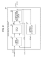
- a clock generation circuit 200 according to the second embodiment is different from the first embodiment in that the phase of the input clock signal CLKIN is controlled to match the phase of the output clock signal CLKOUT.
- FIG. 8 is a block diagram illustrating an example of configuration of the clock generation circuit 200 according to the second embodiment. Therefore, the clock generation circuit 200 according to the second embodiment is different from the first embodiment in that the clock generation circuit 200 according to the second embodiment further includes a time-to-digital converter 260 .
- the time-to-digital converter 260 detects edge positions of the input clock signal CLKIN at a resolution finer than the clock period of the input clock signal CLKIN, and outputs a digital value indicating the detection result.
- This time-to-digital converter 260 uses the output clock signal CLKOUT and the like as the reference clock signal to detect edge positions of the input clock signal CLKIN at a resolution according to the frequency of the reference clock signal. Then, the time-to-digital converter 260 provides the detection result to the phase comparison circuit 210 .
- the phase comparison circuit 210 compares the phase difference between the edge position indicating the detection result and the edge position of the feedback signal fbCLK 1 .
- the resolution of the phase comparison is 1/F (CLKOUT). Even if F (CLKOUT) is high such as 1 GHz, the resolution thereof is about 1 nanosecond (ns).
- F (CLKOUT) is high such as 1 GHz, the resolution thereof is about 1 nanosecond (ns).
- the frequency control is not performed by the oscillator 234 , which causes jitter.
- the time-to-digital converter 260 detects edge positions of the input clock signal CLKIN at the resolution according to the frequency of the output clock signal CLKOUT (reference clock signal). Therefore, the phase resolution can be improved as compared with the first embodiment. Therefore, the jitter is further reduced.
- the non-integral multiplier phase synchronization circuit 230 provides the output clock signal CLKOUT to not only the AD conversion circuit 110 , the logic circuit 120 , and the feedback frequency divider circuit 250 but also the time-to-digital converter 260 .
- the clock generation circuit 200 can detect the edges of the input clock signal on the basis of the reference clock signal of which frequency is higher than the input clock signal, and therefore, the phase resolution can be improved. Therefore, the noises can be further reduced.
- the reference clock signal bCLK is used as the driving clock signal of the digital filter 220 .
- the output clock signal CLKOUT may be used as the driving clock signal instead of the reference clock signal bCLK.
- the clock generation circuit 200 according to the modification of the second embodiment is different from the second embodiment in that the output clock signal CLKOUT is used as the driving clock oscillation instead of the reference clock signal bCLK.
- FIG. 9 is a block diagram illustrating an example of configuration of the clock generation circuit 200 according to the modification of the second embodiment.
- the clock generation circuit 200 according to the modification is different from the second embodiment in that the digital filter 220 operates in synchronization with the output clock signal CLKOUT.
- the digital filter 220 can be caused to operate in synchronization with the output clock signal CLKOUT.
- each of the matters described in the embodiments corresponds to and is related to each of the invention-specifying matters described in the claims.
- there is a corresponding relationship between each of the invention-specifying matters described in the claims corresponds to and is related to each of the matters in the embodiments of the present technique denoted with the same name as the invention-specifying matter described in the claims.
- the present technique is not limited to the embodiments, and may be embodied by applying various modifications to the embodiments without deviating from the gist thereof.
- the processing procedure explained in the above embodiments may be understood as a method having the series of procedures, and may be understood as a program for causing a computer to execute the series of procedures and a recording medium storing the program.
- Examples of recording media can include a CD (Compact Disc), an MD (MiniDisc), a DVD (Digital Versatile Disc), memory card, Blu-ray (registered trademark) Disc, and the like.
- the present technique may be configured as follows.
- a clock generation circuit including:
- phase difference comparison circuit configured to compare a phase of each of an input clock signal and a feedback signal which have been received, and provides a phase difference signal indicating a phase difference between the input clock signal and the feedback signal;
- a filter circuit configured to suppress a high frequency component, of which frequency is higher than a predetermined cutoff frequency, in the phase difference signal
- an output circuit configured to modulate the phase difference signal, of which high frequency component is suppressed, in such a manner as to decrease a noise component of a low frequency band and increase a noise component of a high frequency band, and generate and output an output clock signal from the modulated phase difference signal and a reference clock signal;
- a frequency dividing circuit configured to divide a frequency of the output clock signal, which has been output, at a predetermined frequency dividing ratio, and feed the output clock signal back to the phase comparison circuit as the feedback signal.
- the output circuit includes:
- a modulator configured to modulate the phase difference signal of which high frequency component has been suppressed
- a multiplier circuit configured to multiply the reference clock signal by a multiplication ratio according to the phase difference indicated by the frequency dividing ratio setting signal which has been modulated, and output the output clock signal.
- the output circuit further includes an adjustment unit configured to adjust the phase difference indicated by the phase difference signal so that it attains a value obtained by multiplying a ratio of a frequency of the reference clock signal with respect to a frequency of the input clock signal by the predetermined frequency dividing ratio, and input the phase difference signal indicating the adjusted value into the modulator.
- multiplier circuit includes:
- phase difference detector configured to compare phases of the reference clock signal and an internal signal, and detect a phase difference between the reference clock signal and the internal signal
- an oscillator configured to oscillate at a frequency according to the phase difference detected by the phase difference detector, and generate the output clock signal
- variable frequency divider configured to divide a frequency of the output clock signal, which has been generated, at a frequency dividing ratio equal to the value indicated by the phase difference signal which has been modulated, and feed the output clock signal back to the phase difference detector as the internal signal.
- the clock generation circuit according to any one of (1) to (4) further including a detection circuit configured to provide the phase comparison circuit with a detection result obtained by detecting an edge of the input clock signal on the basis of a reference clock signal of a frequency higher than the input clock signal.
- An electronic device including:
- a reference clock providing circuit configured to provide
- phase difference comparison circuit configured to compare a phase of each of an input clock signal and a feedback signal which have been input, and provides a phase difference signal indicating a phase difference between the input clock signal and the feedback signal;
- a filter circuit configured to suppress a high frequency component, of which frequency is higher than a predetermined cutoff frequency, in the phase difference signal
- an output circuit configured to modulate the phase difference signal, of which high frequency component is suppressed, in such a manner as to decrease a noise component of a low frequency band and increase a noise component of a high frequency band, and generate and output an output clock signal from the modulated phase difference signal and a reference clock signal; and a frequency dividing circuit configured to divide a frequency of the output clock signal, which has been output, at a predetermined frequency dividing ratio, and feed the output clock signal back to the phase comparison circuit as the feedback signal.
Abstract
Description
F(CLKOUT)=F(bCLK)×AVG(N) Expression 1
AVG(N)=F(CLKIN)×Nc×1/F(bCLK) Expression 2
- 100 Electronic device
- 110 AD conversion circuit
- 120 Logic circuit
- 200 Clock generation circuit
- 210 Phase comparison circuit
- 220 Digital filter
- 230 Non-integral multiplier phase synchronization circuit
- 231 Multiplier circuit
- 232 Phase difference detector
- 233 Low pass filter
- 234 Oscillator
- 235 Variable frequency divider
- 236 Adder
- 237 Reference clock frequency divider
- 238 Output clock frequency divider
- 240 Sigma delta modulator
- 241 Subtracter
- 242 Integrator
- 243 Adder
- 244, 246 Delay memory
- 245 Quantizer
- 250 Feedback frequency divider circuit
- 260 Time-to-digital converter
Claims (8)
Applications Claiming Priority (2)
| Application Number | Priority Date | Filing Date | Title |
|---|---|---|---|
| JP2013-254860 | 2013-12-10 | ||
| JP2013254860A JP2015114749A (en) | 2013-12-10 | 2013-12-10 | Clock generation circuit |
Publications (2)
| Publication Number | Publication Date |
|---|---|
| US20150162917A1 US20150162917A1 (en) | 2015-06-11 |
| US9484948B2 true US9484948B2 (en) | 2016-11-01 |
Family
ID=53272212
Family Applications (1)
| Application Number | Title | Priority Date | Filing Date |
|---|---|---|---|
| US14/539,293 Active 2034-11-28 US9484948B2 (en) | 2013-12-10 | 2014-11-12 | Clock generation circuit |
Country Status (2)
| Country | Link |
|---|---|
| US (1) | US9484948B2 (en) |
| JP (1) | JP2015114749A (en) |
Families Citing this family (8)
| Publication number | Priority date | Publication date | Assignee | Title |
|---|---|---|---|---|
| JP6919154B2 (en) | 2016-03-31 | 2021-08-18 | ソニーグループ株式会社 | Solid-state image sensor, image sensor, and electronic equipment |
| JP6834299B2 (en) | 2016-09-27 | 2021-02-24 | セイコーエプソン株式会社 | Circuit devices, physical quantity measuring devices, electronic devices and mobile objects |
| US10291386B2 (en) | 2017-09-29 | 2019-05-14 | Cavium, Llc | Serializer/deserializer (SerDes) lanes with lane-by-lane datarate independence |
| US10110240B1 (en) * | 2017-10-17 | 2018-10-23 | Micron Technology, Inc. | DLL circuit having variable clock divider |
| US10431281B1 (en) * | 2018-08-17 | 2019-10-01 | Micron Technology, Inc. | Access schemes for section-based data protection in a memory device |
| US10991411B2 (en) | 2018-08-17 | 2021-04-27 | Micron Technology, Inc. | Method and apparatuses for performing a voltage adjustment operation on a section of memory cells based on a quantity of access operations |
| US10516403B1 (en) * | 2019-02-27 | 2019-12-24 | Ciena Corporation | High-order phase tracking loop with segmented proportional and integral controls |
| CN115378567B (en) * | 2022-08-19 | 2023-07-18 | 深圳市紫光同创电子有限公司 | Clock synchronization circuit, clock synchronization method and electronic equipment |
Citations (7)
| Publication number | Priority date | Publication date | Assignee | Title |
|---|---|---|---|---|
| US7415092B2 (en) * | 2003-12-15 | 2008-08-19 | Aktino, Inc. | Low wander timing generation and recovery |
| US7436227B2 (en) * | 2003-05-02 | 2008-10-14 | Silicon Laboratories Inc. | Dual loop architecture useful for a programmable clock source and clock multiplier applications |
| US7548121B2 (en) * | 2005-08-18 | 2009-06-16 | Realtek Semiconductor Corp. | Fractional frequency synthesizer and phase locked loop utilizing fractional frequency synthesizer and method thereof |
| US7583774B2 (en) * | 2003-12-17 | 2009-09-01 | Wolfson Microelectronics Plc | Clock synchroniser |
| US7679454B2 (en) * | 2006-10-23 | 2010-03-16 | Realtek Semiconductor Corp. | Hybrid phase-locked loop |
| JP2013005050A (en) | 2011-06-13 | 2013-01-07 | Sony Corp | Clock generation device and electronic apparatus |
| US8674731B1 (en) * | 2013-01-22 | 2014-03-18 | Applied Micro Circuits Corporations | Fractional phase-locked loop with dynamic divide ratio adjustment |
-
2013
- 2013-12-10 JP JP2013254860A patent/JP2015114749A/en active Pending
-
2014
- 2014-11-12 US US14/539,293 patent/US9484948B2/en active Active
Patent Citations (7)
| Publication number | Priority date | Publication date | Assignee | Title |
|---|---|---|---|---|
| US7436227B2 (en) * | 2003-05-02 | 2008-10-14 | Silicon Laboratories Inc. | Dual loop architecture useful for a programmable clock source and clock multiplier applications |
| US7415092B2 (en) * | 2003-12-15 | 2008-08-19 | Aktino, Inc. | Low wander timing generation and recovery |
| US7583774B2 (en) * | 2003-12-17 | 2009-09-01 | Wolfson Microelectronics Plc | Clock synchroniser |
| US7548121B2 (en) * | 2005-08-18 | 2009-06-16 | Realtek Semiconductor Corp. | Fractional frequency synthesizer and phase locked loop utilizing fractional frequency synthesizer and method thereof |
| US7679454B2 (en) * | 2006-10-23 | 2010-03-16 | Realtek Semiconductor Corp. | Hybrid phase-locked loop |
| JP2013005050A (en) | 2011-06-13 | 2013-01-07 | Sony Corp | Clock generation device and electronic apparatus |
| US8674731B1 (en) * | 2013-01-22 | 2014-03-18 | Applied Micro Circuits Corporations | Fractional phase-locked loop with dynamic divide ratio adjustment |
Also Published As
| Publication number | Publication date |
|---|---|
| JP2015114749A (en) | 2015-06-22 |
| US20150162917A1 (en) | 2015-06-11 |
Similar Documents
| Publication | Publication Date | Title |
|---|---|---|
| US9484948B2 (en) | Clock generation circuit | |
| US20200321968A1 (en) | Digital-to-time converter (dtc) assisted all digital phase locked loop (adpll) circuit | |
| US8787515B2 (en) | Clock data recovery circuit | |
| US8451971B2 (en) | Communication systems, clock generation circuits thereof, and method for generating clock signal | |
| US8368435B2 (en) | Method and apparatus for jitter reduction | |
| US8433024B2 (en) | Spread spectrum clock generator and method for adjusting spread amount | |
| US8446194B2 (en) | Spread spectrum clock generating circuit | |
| US7679454B2 (en) | Hybrid phase-locked loop | |
| US7636018B2 (en) | Phase locked loop with phase shifted input | |
| US8988121B2 (en) | Method and apparatus for generating a reference signal for a fractional-N frequency synthesizer | |
| US20200195263A1 (en) | Apparatus for Digital Frequency Synthesizers and Associated Methods | |
| US8531214B2 (en) | Spread spectrum clock generators | |
| US8674731B1 (en) | Fractional phase-locked loop with dynamic divide ratio adjustment | |
| KR20170083816A (en) | Digital phase locked loop and driving method thereof | |
| US9019016B2 (en) | Accumulator-type fractional N-PLL synthesizer and control method thereof | |
| JP2007295363A (en) | Pll circuit, method for preventing interference of the pll circuit, and optical disk device having pll circuit mounted thereon | |
| US8130048B2 (en) | Local oscillator | |
| US8664989B1 (en) | Method to increase frequency resolution of a fractional phase-locked loop | |
| US10148275B1 (en) | Low power digital-to-analog converter (DAC)-based frequency synthesizer | |
| US9680495B1 (en) | Data conversion | |
| KR20160149362A (en) | Phase locked loop and operating method thereof | |
| JP6779419B2 (en) | Phase-locked loop | |
| WO2012093424A1 (en) | Delta-sigma modulating fractional-n pll frequency synthesizer and wireless communication device equipped with same | |
| JPWO2006114941A1 (en) | Clock generation circuit and audio system | |
| US8656203B2 (en) | Fractional frequency division or multiplication by using an oversampled phase rotator for reducing jitter |
Legal Events
| Date | Code | Title | Description |
|---|---|---|---|
| AS | Assignment |
Owner name: SONY CORPORATION, JAPAN Free format text: ASSIGNMENT OF ASSIGNORS INTEREST;ASSIGNOR:TSUKUDA, YASUNORI;REEL/FRAME:034156/0096 Effective date: 20141031 |
|
| AS | Assignment |
Owner name: SONY SEMICONDUCTOR SOLUTIONS CORPORATION, JAPAN Free format text: ASSIGNMENT OF ASSIGNORS INTEREST;ASSIGNOR:SONY CORPORATION;REEL/FRAME:039645/0019 Effective date: 20160708 |
|
| STCF | Information on status: patent grant |
Free format text: PATENTED CASE |
|
| FEPP | Fee payment procedure |
Free format text: PAYOR NUMBER ASSIGNED (ORIGINAL EVENT CODE: ASPN); ENTITY STATUS OF PATENT OWNER: LARGE ENTITY |
|
| AS | Assignment |
Owner name: SONY SEMICONDUCTOR SOLUTIONS CORPORATION, JAPAN Free format text: CORRECTIVE ASSIGNMENT TO CORRECT THE ASSIGNEE ZIP CODE FROM 246-0014 TO 243-0014 PREVIOUSLY RECORDED AT REEL: 039645 FRAME: 0019. ASSIGNOR(S) HEREBY CONFIRMS THE ASSIGNMENT;ASSIGNOR:SONY CORPORATION;REEL/FRAME:040894/0926 Effective date: 20160708 |
|
| MAFP | Maintenance fee payment |
Free format text: PAYMENT OF MAINTENANCE FEE, 4TH YEAR, LARGE ENTITY (ORIGINAL EVENT CODE: M1551); ENTITY STATUS OF PATENT OWNER: LARGE ENTITY Year of fee payment: 4 |