US9501169B2 - Acquiring multiple capacitive partial profiles with orthogonal sensor electrodes - Google Patents
Acquiring multiple capacitive partial profiles with orthogonal sensor electrodes Download PDFInfo
- Publication number
- US9501169B2 US9501169B2 US14/318,219 US201414318219A US9501169B2 US 9501169 B2 US9501169 B2 US 9501169B2 US 201414318219 A US201414318219 A US 201414318219A US 9501169 B2 US9501169 B2 US 9501169B2
- Authority
- US
- United States
- Prior art keywords
- capacitive
- sensor
- sensor electrodes
- driving
- sensor electrode
- Prior art date
- Legal status (The legal status is an assumption and is not a legal conclusion. Google has not performed a legal analysis and makes no representation as to the accuracy of the status listed.)
- Active, expires
Links
Images


Classifications
-
- G—PHYSICS
- G06—COMPUTING; CALCULATING OR COUNTING
- G06F—ELECTRIC DIGITAL DATA PROCESSING
- G06F3/00—Input arrangements for transferring data to be processed into a form capable of being handled by the computer; Output arrangements for transferring data from processing unit to output unit, e.g. interface arrangements
- G06F3/01—Input arrangements or combined input and output arrangements for interaction between user and computer
- G06F3/03—Arrangements for converting the position or the displacement of a member into a coded form
- G06F3/041—Digitisers, e.g. for touch screens or touch pads, characterised by the transducing means
- G06F3/0416—Control or interface arrangements specially adapted for digitisers
- G06F3/04166—Details of scanning methods, e.g. sampling time, grouping of sub areas or time sharing with display driving
-
- G—PHYSICS
- G06—COMPUTING; CALCULATING OR COUNTING
- G06F—ELECTRIC DIGITAL DATA PROCESSING
- G06F3/00—Input arrangements for transferring data to be processed into a form capable of being handled by the computer; Output arrangements for transferring data from processing unit to output unit, e.g. interface arrangements
- G06F3/01—Input arrangements or combined input and output arrangements for interaction between user and computer
- G06F3/03—Arrangements for converting the position or the displacement of a member into a coded form
- G06F3/041—Digitisers, e.g. for touch screens or touch pads, characterised by the transducing means
- G06F3/0416—Control or interface arrangements specially adapted for digitisers
- G06F3/0418—Control or interface arrangements specially adapted for digitisers for error correction or compensation, e.g. based on parallax, calibration or alignment
-
- G—PHYSICS
- G06—COMPUTING; CALCULATING OR COUNTING
- G06F—ELECTRIC DIGITAL DATA PROCESSING
- G06F3/00—Input arrangements for transferring data to be processed into a form capable of being handled by the computer; Output arrangements for transferring data from processing unit to output unit, e.g. interface arrangements
- G06F3/01—Input arrangements or combined input and output arrangements for interaction between user and computer
- G06F3/03—Arrangements for converting the position or the displacement of a member into a coded form
- G06F3/041—Digitisers, e.g. for touch screens or touch pads, characterised by the transducing means
- G06F3/044—Digitisers, e.g. for touch screens or touch pads, characterised by the transducing means by capacitive means
- G06F3/0446—Digitisers, e.g. for touch screens or touch pads, characterised by the transducing means by capacitive means using a grid-like structure of electrodes in at least two directions, e.g. using row and column electrodes
-
- G—PHYSICS
- G06—COMPUTING; CALCULATING OR COUNTING
- G06F—ELECTRIC DIGITAL DATA PROCESSING
- G06F2203/00—Indexing scheme relating to G06F3/00 - G06F3/048
- G06F2203/041—Indexing scheme relating to G06F3/041 - G06F3/045
- G06F2203/04105—Pressure sensors for measuring the pressure or force exerted on the touch surface without providing the touch position
-
- G—PHYSICS
- G06—COMPUTING; CALCULATING OR COUNTING
- G06F—ELECTRIC DIGITAL DATA PROCESSING
- G06F2203/00—Indexing scheme relating to G06F3/00 - G06F3/048
- G06F2203/041—Indexing scheme relating to G06F3/041 - G06F3/045
- G06F2203/04108—Touchless 2D- digitiser, i.e. digitiser detecting the X/Y position of the input means, finger or stylus, also when it does not touch, but is proximate to the digitiser's interaction surface without distance measurement in the Z direction
Definitions
- Embodiments of the present invention generally relate to a method and apparatus for performing interleaved capacitive sensing to improve sensing performance.
- proximity sensor devices also commonly called touchpads or touch sensor devices
- a proximity sensor device typically includes a sensing region, often demarked by a surface, in which the proximity sensor device determines the presence, location and/or motion of one or more input objects.
- Proximity sensor devices may be used to provide interfaces for the electronic system.
- proximity sensor devices are often used as input devices for larger computing systems (such as opaque touchpads integrated in, or peripheral to, notebook or desktop computers).
- proximity sensor devices are also often used in smaller computing systems (such as touch screens integrated in cellular phones or tablet computers).
- One embodiment described herein is a processing system comprising a sensor module coupled to a plurality of sensor electrodes, where the sensor module is configured to drive various ones of the plurality of sensor electrodes.
- the sensor module simultaneously drives a capacitive sensing signal onto a first sensor electrode of the plurality of sensor electrodes, and a substantially constant voltage onto a second sensor electrode of the plurality of sensor electrodes.
- the sensor module acquires a first capacitive partial profile based on the driven capacitive sensing signal.
- the sensor module simultaneously drives the capacitive sensing signal onto the second sensor electrode and the substantially constant voltage onto the first sensor electrode.
- the sensor module acquires a second capacitive partial profile based on the driven capacitive sensing signal.
- the sensor module also drives one or more sensor electrodes of a second plurality of sensor electrodes with the substantially constant voltage, the second plurality of sensor electrodes disposed substantially orthogonal to the first plurality of sensor electrodes.
- the processing system further includes a determination module that determines a first capacitive profile based on at least the acquired first and second capacitive partial profiles.
- Another embodiment described herein is a method for driving a plurality of sensor electrodes for capacitive sensing, in which a first capacitive partial profile is acquired during a first time period by driving a capacitive sensing signal onto a first sensor electrode of a first plurality of sensor electrodes, while driving a second sensor electrode of the first plurality of sensor electrodes with a substantially constant voltage.
- a second capacitive partial profile is acquired by driving the capacitive sensing signal onto the second sensor electrode while driving the first sensor electrode with the substantially constant voltage.
- the method further includes driving one or more sensor electrodes of a second plurality of sensor electrodes with the substantially constant voltage during at least one of the first and second time periods, and determining a first capacitive profile for a sensing region based on at least the first and second capacitive partial profiles.
- the second plurality of sensor electrodes is disposed substantially orthogonal to the first plurality of sensor electrodes.
- an input device comprising a plurality of sensor electrodes, which includes a first plurality of sensor electrodes arranged along a first sensing axis.
- the input device further comprises a processing system coupled to the plurality of sensor electrodes and configured to acquire a first capacitive partial image during a first time period by driving a capacitive sensing signal onto a first sensor electrode of the first plurality of sensor electrodes, while driving a second sensor electrode of the first plurality of sensor electrodes with a substantially constant voltage.
- the processing system acquires a second capacitive partial image by driving the capacitive sensing signal onto the second sensor electrode while driving the first sensor electrode with the substantially constant voltage.
- the processing system of the input device is further configured to determine a first capacitive profile based on at least the first and second capacitive partial profiles.
- FIG. 1 is a schematic block diagram of an input device, according to embodiments described herein.
- FIGS. 2A and 2B illustrate portions of exemplary patterns of sensing elements or capacitive sensing pixels, according to embodiments described herein.
- FIGS. 3A and 3B illustrate a portion of a pattern of sensing elements configured to perform interleaved capacitive sensing for a sensing region, according to one embodiment.
- FIGS. 4A-4D illustrate a portion of a pattern of sensing elements configured to perform interleaved capacitive sensing for a sensing region, according to one embodiment.
- FIGS. 5A and 5B illustrate a portion of a pattern of sensing elements configured to perform interleaved capacitive sensing for a sensing region, according to one embodiment.
- FIGS. 6A-6D illustrate a portion of a pattern of sensing elements configured to perform interleaved capacitive sensing for a sensing region, according to one embodiment.
- FIG. 7 illustrates a method for interleaved capacitive sensing, according to one embodiment described herein.
- an input device acquires a first capacitive partial profile during a first time period by driving a capacitive sensing signal onto a first sensor electrode of a first plurality of sensor electrodes, while driving a second sensor electrode of the first plurality of sensor electrodes with a substantially constant voltage.
- the input device generates a second capacitive partial profile by driving the capacitive sensing signal onto the second sensor electrode while driving the first sensor electrode with the substantially constant voltage.
- one or more sensor electrodes of a second plurality of sensor electrodes disposed orthogonal to the first plurality are driven with the substantially constant voltage.
- the input device determines a first capacitive profile for a sensing region based on at least the first and second capacitive partial profiles.
- the input device may improve its ability to detect input objects, including those that are ungrounded or weakly grounded. By improving detectability of these input objects, measurement accuracy and capacitive sensing performance may also be improved.
- FIG. 1 is a schematic block diagram of an input device 100 , in accordance with embodiments described herein.
- the input device 100 may be configured to provide input to an electronic system 150 .
- the term “electronic system” broadly refers to any system capable of electronically processing information.
- electronic systems include personal computers of all sizes and shapes, such as desktop computers, laptop computers, netbook computers, tablets, web browsers, e-book readers, and personal digital assistants (PDAs).
- Additional example electronic systems include composite input devices, such as physical keyboards that include input device 100 and separate joysticks or key switches.
- peripherals such as data input devices (including remote controls and mice), and data output devices (including display screens and printers).
- remote terminals e.g., video game consoles, portable gaming devices, and the like.
- video game machines e.g., video game consoles, portable gaming devices, and the like.
- communication devices including cellular phones, such as smart phones
- media devices including recorders, editors, and players such as televisions, set-top boxes, music players, digital photo frames, and digital cameras.
- the electronic system could be a host or a slave to the input device.
- the input device 100 can be implemented as a physical part of the electronic system 150 , or can be physically separate from the electronic system. As appropriate, the input device 100 may communicate with parts of the electronic system using any one or more of the following: buses, networks, and other wired or wireless interconnections. Examples include I 2 C, SPI, PS/2, Universal Serial Bus (USB), Bluetooth, RF, and IRDA.
- buses, networks, and other wired or wireless interconnections examples include I 2 C, SPI, PS/2, Universal Serial Bus (USB), Bluetooth, RF, and IRDA.
- the input device 100 is shown as a proximity sensor device (also often referred to as a “touchpad” or a “touch sensor device”) configured to sense input provided by one or more input objects 140 in a sensing region 120 .
- Example input objects include fingers and styli, as shown in FIG. 1 .
- Sensing region 120 encompasses any space above, around, in and/or near the input device 100 in which the input device 100 is able to detect user input (e.g., user input provided by one or more input objects 140 ).
- the sizes, shapes, and locations of particular sensing regions may vary widely from embodiment to embodiment.
- the sensing region 120 extends from a surface of the input device 100 in one or more directions into space until signal-to-noise ratios prevent sufficiently accurate object detection.
- the distance to which this sensing region 120 extends in a particular direction in various embodiments, may be on the order of less than a millimeter, millimeters, centimeters, or more, and may vary significantly with the type of sensing technology used and the accuracy desired.
- some embodiments sense input that comprises no contact with any surfaces of the input device 100 , contact with an input surface (e.g. a touch surface) of the input device 100 , contact with an input surface of the input device 100 coupled with some amount of applied force or pressure, and/or a combination thereof.
- input surfaces may be provided by surfaces of casings within which the sensor electrodes reside, by face sheets applied over the sensor electrodes or any casings, etc.
- the sensing region 120 has a rectangular shape when projected onto an input surface of the input device 100 .
- the input device 100 may utilize any combination of sensor components and sensing technologies to detect user input in the sensing region 120 .
- the input device 100 comprises a plurality of sensing elements 121 for detecting user input.
- the input device 100 may include one or more sensing elements 121 that are combined to form sensor electrodes.
- the input device 100 may use capacitive, elastive, resistive, inductive, magnetic acoustic, ultrasonic, and/or optical techniques.
- Some implementations are configured to provide images that span one, two, three, or higher dimensional spaces. Some implementations are configured to provide projections of input along particular axes or planes.
- a flexible and conductive first layer is separated by one or more spacer elements from a conductive second layer.
- one or more voltage gradients are created across the layers. Pressing the flexible first layer may deflect it sufficiently to create electrical contact between the layers, resulting in voltage outputs reflective of the point(s) of contact between the layers. These voltage outputs may be used to determine positional information.
- one or more sensing elements 121 pick up loop currents induced by a resonating coil or pair of coils. Some combination of the magnitude, phase, and frequency of the currents may then be used to determine positional information.
- voltage or current is applied to create an electric field. Nearby input objects cause changes in the electric field, and produce detectable changes in capacitive coupling that may be detected as changes in voltage, current, or the like.
- Some capacitive implementations utilize arrays or other regular or irregular patterns of capacitive sensing elements 121 to create electric fields.
- separate sensing elements 121 may be ohmically shorted together to form larger sensor electrodes.
- Some capacitive implementations utilize resistive sheets, which may be uniformly resistive.
- the sensing elements 121 may be capacitive sensing pixels that include one or more sensor or other electrodes.
- Some capacitive implementations utilize “self capacitance” (or “absolute capacitance”) sensing methods based on changes in the capacitive coupling between sensor electrodes and an input object.
- an input object near the sensor electrodes alters the electric field near the sensor electrodes, thus changing the measured capacitive coupling.
- an absolute capacitance sensing method operates by modulating sensor electrodes with respect to a reference voltage (e.g. system ground), and by detecting the capacitive coupling between the sensor electrodes and input objects.
- Some capacitive implementations utilize “mutual capacitance” (or “transcapacitance”) sensing methods based on changes in the capacitive coupling between sensor electrodes.
- the change in capacitive coupling may be between sensor electrodes in two different sensing elements 121 or between two different sensor electrodes in the same sensing element 121 .
- an input object near the sensor electrodes alters the electric field between the sensor electrodes, thus changing the measured capacitive coupling.
- a transcapacitance sensing method operates by detecting the capacitive coupling between one or more transmitter sensor electrodes (also “transmitter electrodes”) and one or more receiver sensor electrodes (also “receiver electrodes”).
- the processing system 110 is shown as part of the input device 100 .
- the processing system 110 is configured to operate the hardware of the input device 100 to detect input in the sensing region 120 .
- the processing system 110 comprises parts of or all of one or more integrated circuits (ICs) and/or other circuitry components.
- ICs integrated circuits
- a processing system for a mutual capacitance sensor device may comprise transmitter circuitry configured to transmit signals with transmitter sensor electrodes, and/or receiver circuitry configured to receive signals with receiver sensor electrodes.
- the processing system 110 also comprises electronically-readable instructions, such as firmware code, software code, and/or the like.
- components composing the processing system 110 are located together, such as near sensing element(s) 121 of the input device 100 .
- components of processing system 110 are physically separate with one or more components close to sensing element(s) 121 of input device 100 , and one or more components elsewhere.
- the input device 100 may be a peripheral coupled to a desktop computer, and the processing system 110 may comprise software configured to run on a central processing unit of the desktop computer and one or more ICs (perhaps with associated firmware) separate from the central processing unit.
- the input device 100 may be physically integrated in a phone, and the processing system 110 may comprise circuits and firmware that are part of a main processor of the phone.
- the processing system 110 is dedicated to implementing the input device 100 .
- the processing system 110 also performs other functions, such as operating display screens, driving haptic actuators, etc.
- the processing system 110 may be implemented as a set of modules that handle different functions of the processing system 110 .
- Each module may comprise circuitry that is a part of the processing system 110 , firmware, software, or a combination thereof.
- Example modules include hardware operation modules for operating hardware such as sensor electrodes and display screens, data processing modules for processing data such as sensor signals and positional information, and reporting modules for reporting information.
- Further example modules include sensor operation modules configured to operate sensing elements 121 to detect input, identification modules configured to identify gestures such as mode changing gestures, and mode changing modules for changing operation modes.
- processing system 110 includes at least one sensor module, and a display driver module, each of which will be described more fully below.
- the processing system 110 responds to user input (or lack of user input) in the sensing region 120 directly by causing one or more actions.
- Example actions include changing operation modes, as well as GUI actions such as cursor movement, selection, menu navigation, and other functions.
- the processing system 110 provides information about the input (or lack of input) to some part of the electronic system (e.g., to a central processing system of the electronic system that is separate from the processing system 110 , if such a separate central processing system exists).
- some part of the electronic system processes information received from the processing system 110 to act on user input, such as to facilitate a full range of actions, including mode changing actions and GUI actions.
- the processing system 110 operates the sensing element(s) 121 of the input device 100 to produce electrical signals indicative of input (or lack of input) in the sensing region 120 .
- the processing system 110 may perform any appropriate amount of processing on the electrical signals in producing the information provided to the electronic system.
- the processing system 110 may digitize analog electrical signals obtained from the sensing elements 121 .
- the processing system 110 may perform filtering or other signal conditioning.
- the processing system 110 may subtract or otherwise account for a baseline, such that the information reflects a difference between the electrical signals and the baseline.
- the processing system 110 may determine positional information, recognize inputs as commands, recognize handwriting, and the like.
- Positional information as used herein broadly encompasses absolute position, relative position, velocity, acceleration, and other types of spatial information.
- Exemplary “zero-dimensional” positional information includes near/far or contact/no contact information.
- Exemplary “one-dimensional” positional information includes positions along an axis.
- Exemplary “two-dimensional” positional information includes motions in a plane.
- Exemplary “three-dimensional” positional information includes instantaneous or average velocities in space. Further examples include other representations of spatial information.
- Historical data regarding one or more types of positional information may also be determined and/or stored, including, for example, historical data that tracks position, motion, or instantaneous velocity over time.
- the input device 100 comprises a display region 145 in addition to the sensing region 120 (e.g., a touch screen interface), and the sensing region 120 overlaps at least part of an active area of a display screen of the display region 145 .
- the input device 100 may comprise substantially transparent sensing elements overlaying the display screen and provide a touch screen interface for the associated electronic system.
- the display screen may be any type of dynamic display capable of displaying a visual interface to a user, and may include any type of light emitting diode (LED), organic LED (OLED), cathode ray tube (CRT), liquid crystal display (LCD), plasma, electroluminescence (EL), or other display technology.
- the sensing region 120 and the display region 145 may share physical elements. For example, some embodiments may utilize some of the same electrical components for displaying and for sensing.
- the display device may be operated in part or in total by the processing system 110 (e.g., by display driver module 215 ).
- the mechanisms of the present technology are capable of being distributed as a program product (e.g., software) in a variety of forms.
- the mechanisms of the present technology may be implemented and distributed as a software program on information bearing media that are readable by electronic processors (e.g., non-transitory computer-readable and/or recordable/writable information bearing media readable by the processing system 110 ).
- the embodiments of the present technology apply equally regardless of the particular type of medium used to carry out the distribution. Examples of non-transitory, electronically readable media include various discs, memory sticks, memory cards, memory modules, and the like. Electronically readable media may be based on flash, optical, magnetic, holographic, or any other storage technology.
- FIG. 2A illustrates a portion of a pattern of sensing elements configured to sense in a sensing region 120 associated with the pattern, according to several embodiments.
- This pattern of sensing elements comprises a first plurality of sensor electrodes 205 ( 205 1 , 205 2 , 205 3 , . . . 205 m ), and a second plurality of sensor electrodes 215 ( 215 1 , 215 2 , 215 3 , . . . 215 n ) disposed over the plurality of sensor electrodes 205 .
- processing system 110 operates the first plurality of sensor electrodes 205 as a plurality of transmitter electrodes, and the second plurality of sensor electrodes 215 as a plurality of receiver electrodes. In another embodiment, processing system 110 operates the first plurality of sensor electrodes 205 and the second plurality of sensor electrodes 215 as absolute capacitive sensing electrodes.
- the first plurality of sensor electrodes 205 and the second plurality of sensor electrodes 215 are typically ohmically isolated from each other. That is, one or more insulators separate the first plurality of sensor electrodes 205 and the second plurality of sensor electrodes 215 and prevent them from electrically shorting to each other.
- the first plurality of sensor electrodes 205 and the second plurality of sensor electrodes 215 may be disposed on a common layer.
- the pluralities of sensor electrodes 205 , 215 may be electrically separated by insulative material disposed between them at cross-over areas; in such constructions, the first plurality of sensor electrodes 205 and/or the second plurality of sensor electrodes 215 may be formed with jumpers connecting different portions of the same electrode.
- the first plurality of sensor electrodes 205 and the second plurality of sensor electrodes 215 are separated by one or more layers of insulative material. In some embodiments, the first plurality of sensor electrodes 205 and the second plurality of sensor electrodes 215 are separated by one or more substrates; for example, they may be disposed on opposite sides of the same substrate, or on different substrates that are laminated together. In some embodiments, the first plurality of sensor electrodes 205 and the second plurality of sensor electrodes 215
- the first plurality of sensor electrodes 205 may extend in a first direction while the second plurality of sensor electrodes 215 extend in a second direction. As shown in FIG. 2A , the first plurality of sensor electrodes 205 extend in one direction, while the second plurality of sensor electrodes 215 extend in a direction substantially orthogonal to the transmitter electrodes. Of course, other orientations are possible (e.g., parallel or other relative orientations).
- the areas of localized capacitive coupling between the first plurality of sensor electrodes 205 and the second plurality of sensor electrodes 215 may be termed “capacitive pixels.”
- the capacitive coupling between the first plurality of sensor electrodes 205 and the second plurality of sensor electrodes 215 change with the proximity and motion of input objects in the sensing region associated with the first plurality of sensor electrodes 205 and the second plurality of sensor electrodes 215 .
- FIG. 2B illustrates a portion of a pattern of capacitive sensing pixels 225 (also referred to herein as capacitive pixels or sensing pixels) configured to sense in the sensing region 120 associated with a pattern, according to some embodiments.
- Each capacitive pixel 225 may include one of more of the sensing elements described above.
- a respective sensor electrode may correspond to each capacitive pixel (i.e., in a 1:1 ratio), and each of the sensor electrodes may have a similar shape, size, and/or alignment with its respective capacitive pixel.
- FIG. 2B illustrates a portion of a pattern of capacitive sensing pixels 225 (also referred to herein as capacitive pixels or sensing pixels) configured to sense in the sensing region 120 associated with a pattern, according to some embodiments.
- Each capacitive pixel 225 may include one of more of the sensing elements described above.
- a respective sensor electrode may correspond to each capacitive pixel (i.e., in a 1:1 ratio), and
- FIG. 2A presents the regions of the capacitive pixels 225 in a pattern of simple rectangles and does not show various other components within the capacitive pixels 225 .
- the capacitive sensing pixels 225 are areas of localized capacitance (capacitive coupling). Capacitive pixels 225 may be formed between an individual sensor electrode and ground in a first mode of operation and between groups of sensor electrodes used as transmitter and receiver electrodes in a second mode of operation. The capacitive coupling changes with the proximity and motion of input objects in the sensing region 120 associated with the capacitive pixels 225 , and thus may be used as an indicator of the presence of the input object in the sensing region 120 of the input device.
- the exemplary pattern comprises an array of capacitive sensing pixels 225 X,Y arranged in a matrix array of X columns and Y rows, where X and Y are positive integers. It is contemplated that the pattern of sensing pixels 225 may comprises a plurality of sensing pixels 225 having other configurations, such as polar arrays, repeating patterns, non-repeating patterns, non-uniform arrays a single row or column, or other suitable arrangement. As shown here, the sensing pixels 225 are coupled to the processing system 110 and utilized to determine the presence (or lack thereof) of an input object in the sensing region 120 .
- At least one sensor electrode within the capacitive sensing pixels 225 may be utilized to detect the presence of an input object via absolute sensing techniques.
- Processing system 110 is configured to drive a sensor electrode in each capacitive pixel 225 with a modulated signal and measure a capacitance between the sensor electrode and the input object (e.g., free space or earth ground) based on the modulated signal, which is utilized by the processing system 110 or other processor to determine the position of the input object.
- the input object e.g., free space or earth ground
- sensor electrodes in the capacitive pixels 225 are utilized to detect the presence of an input object via transcapacitance sensing techniques. That is, processing system 110 may drive at least one sensor electrode in a capacitive pixel 225 with a transmitter signal and receive resulting signals using one or more of the other sensor electrodes in the capacitive pixel 225 , where a resulting signal comprising effects corresponding to the transmitter signal. The resulting signals are utilized by the processing system 110 or other processor to determine the position of the input object.
- the input device 100 may be configured to operate in any one of the modes described above.
- the input device 100 may also be configured to switch between any two or more of the modes described above.
- Input device 100 may be configured to perform “hybrid sensing,” where absolute capacitance and transcapacitance techniques are performed in relatively rapid succession.
- a single sensing cycle or period, or sequential sensing cycles or periods may include one or more absolute capacitance measurements and one or more transcapacitance measurements, and the results of each type of measurement may be combined to determine the position of the input object.
- the capacitive pixels 225 are “scanned” to determine these capacitive couplings. That is, in one embodiment, one or more of the sensor electrodes are driven to transmit transmitter signals. Transmitters may be operated such that one transmitter electrode transmits at one time, or multiple transmitter electrodes transmit at the same time. Where multiple transmitter electrodes transmit simultaneously, the multiple transmitter electrodes may transmit the same transmitter signal and effectively produce an effectively larger transmitter electrode. Alternatively, the multiple transmitter electrodes may transmit different transmitter signals. For example, multiple transmitter electrodes may transmit different transmitter signals according to one or more coding schemes that enable their combined effects on the resulting signals of receiver electrodes to be independently determined.
- the sensor electrodes configured as receiver sensor electrodes may be operated singly or multiply to acquire resulting signals.
- the resulting signals may be used to determine measurements of the capacitive couplings at the capacitive pixels 225 .
- “scanning” capacitive pixels 225 to determine these capacitive couplings includes driving with a modulated signal and measuring the absolute capacitance of one or more of the sensor electrodes.
- the sensor electrodes may be operated such that the modulated signal is driven onto a sensor electrode in multiple capacitive pixels 225 at the same time.
- an absolute capacitive measurement may be obtained from each of the one or more capacitive pixels 225 simultaneously.
- the input device 100 simultaneously drives a sensor electrode in a plurality of capacitive pixels 225 and measures an absolute capacitive measurement for each of the capacitive pixels 225 in the same sensing cycle.
- processing system 110 may configured to selectively drive and receive with a portion of sensor electrodes.
- the sensor electrodes may be selected based on, but not limited to, an application running on the host processor, a status of the input device, an operating mode of the sensing device and a determined location of an input device.
- a set of measurements from the capacitive pixels 225 form a capacitive image (also referred to as a capacitive frame) representative of the capacitive couplings at the capacitive pixels 225 as discussed above.
- Multiple capacitive images may be acquired over multiple time periods, and differences between them used to derive information about input in the sensing region. For example, successive capacitive images acquired over successive periods of time can be used to track the motion(s) of one or more input objects entering, exiting, and within the sensing region.
- the background capacitance of a sensor device is the capacitive image associated with no input object in the sensing region.
- the background capacitance changes with the environment and operating conditions, and may be estimated in various ways. For example, some embodiments take “baseline images” when no input object is determined to be in the sensing region, and use those baseline images as estimates of their background capacitances.
- Capacitive images can be adjusted for the background capacitance of the sensor device for more efficient processing. Some embodiments accomplish this by “baselining” measurements of the capacitive couplings at the capacitive pixels to produce a “baselined capacitive image.” That is, some embodiments compare the measurements forming a capacitance image with appropriate “baseline values” of a “baseline image” associated with those pixels, and determine changes from that baseline image.
- one or more of the sensor electrodes in the capacitive pixels 225 include one or more display electrodes used in updating the display of the display screen.
- the display electrodes comprise one or more segments of a Vcom electrode (common electrode), a source drive line, a gate line, an anode electrode or cathode electrode, or any other display element. These display electrodes may be disposed on an appropriate display screen substrate.
- the electrodes may be disposed on a transparent substrate (a glass substrate, TFT glass, or any other transparent material) in some display screens (e.g., In Plane Switching (IPS) or Plane to Line Switching (PLS) Organic Light Emitting Diode (OLED)), on the bottom of the color filter glass of some display screens (e.g., Patterned Vertical Alignment (PVA) or Multi-domain Vertical Alignment (MVA)), over an emissive layer (OLED), etc.
- IPS In Plane Switching
- PLS Plane to Line Switching
- OLED Organic Light Emitting Diode
- PVA Patterned Vertical Alignment
- MVA Multi-domain Vertical Alignment
- an electrode that is used as both a sensor and a display electrode can also be referred to as a combination electrode, since it performs multiple functions.
- FIG. 2B it is explicitly contemplated that alternate configurations and embodiments, such as the configuration of sensor electrodes depicted in FIG. 2A , may include display
- the “capacitive frame rate” (the rate at which successive capacitive images are acquired) may be the same or be different from that of the “display frame rate” (the rate at which the display image is updated, including refreshing the screen to redisplay the same image).
- the two rates differ, successive capacitive images are acquired at different display updating states, and the different display updating states may affect the capacitive images that are acquired. That is, display updating affects, in particular, the background capacitive image.
- the first and second capacitive images may differ due to differences in the background capacitive image associated with the display updating states, and not due to changes in the sensing region. This is more likely where the capacitive sensing and display updating electrodes are in close proximity to each other, or when they are shared (e.g. combination electrodes).
- a capacitive image that is taken during a particular display updating state is considered to be of a particular frame type. That is, a particular frame type is associated with a mapping of a particular capacitive sensing sequence with a particular display sequence.
- a first capacitive image taken during a first display updating state is considered to be of a first frame type
- a second capacitive image taken during a second display updating state is considered to be of a second frame type
- a third capacitive image taken during a first display updating state is considered to be of a third frame type, and so on.
- capacitive images acquired cycle through the frame types and then repeats.
- the processing system 110 coupled to the sensing electrodes includes a sensor module 235 and optionally, a display driver module 245 .
- the sensor module 235 comprises circuitry configured to drive a transmitter signal or a modulated signal onto the sensing electrodes, and to receive the resulting signals on the sensing electrodes during periods in which input sensing is desired.
- the sensor module 235 is configured to drive each sensor electrode with a modulated signal, and to measure a capacitance between the sensor electrode and the input object based on the modulated signal. The measured capacitance may then be utilized by the processing system 110 or other processor to determine the position of the input object.
- the sensor module 235 may comprise circuitry configured to receive a resulting signal with the sensing electrodes, the resulting signal comprising effects corresponding to the transmitter signal during periods in which input sensing is desired. In one or more embodiments, the sensor module 235 is configured to drive a modulated signal onto a first sensor electrode in one of the capacitive pixels 225 and receive a resulting signal corresponding to the modulated signal to determine changes in absolute capacitance of the sensor electrode.
- the sensor module 235 may determine a position of the input object in the sensing region 120 or may provide a signal including information indicative of the resulting signal to a separate module or processor, for example, a determination module or a processor of the electronic device (i.e., a host processor), for determining the position of the input object in the sensing region 120 .
- the sensor module 235 may comprise separate transmitter and/or receiver modules for performing the various functions described herein.
- the sensor module 235 comprises a plurality of receivers, where each receiver may include an analog front end (AFE).
- capacitive sensing (or input sensing) and display updating may occur during at least partially overlapping periods.
- the combination electrode may also be driven for capacitive sensing.
- overlapping capacitive sensing and display updating may include modulating the reference voltage(s) of the display device and/or modulating at least one display electrode for a display in a time period that at least partially overlaps with when the sensor electrodes are configured for capacitive sensing.
- capacitive sensing and display updating may occur during non-overlapping periods, also referred to as non-display update periods.
- the non-display update periods may occur between display line update periods for two display lines of a display frame and may be at least as long in time as the display update period of one display line.
- the non-display update period may be referred to as a long horizontal blanking period, long h-blanking period or a distributed blanking period.
- the non-display update period may comprise horizontal blanking periods and vertical blanking periods.
- Processing system 110 may be configured to drive sensor electrodes for capacitive sensing during any one or more of or any combination of the different non-display update times.
- the display driver module 245 includes circuitry configured to provide display image update information to the display of the display device during non-sensing (e.g., display updating) periods.
- the display driver module 245 may be included with or separate from the sensor module 235 .
- the processing system 110 comprises a first integrated controller comprising the display driver module 245 and at least a portion of the sensor module 235 (e.g., a transmitter module and/or a receiver module).
- the processing system 110 comprises a first integrated controller comprising the display driver module 245 and a second integrated controller comprising the sensor module 235 .
- the processing system comprises a first integrated controller comprising a display driver module 245 and one of a first portion of sensor module 235 , and a second integrated controller comprising a second portion of sensor module 235 .
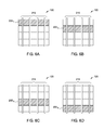
- FIGS. 3A and 3B illustrate a portion of a pattern of sensing elements configured to perform interleaved capacitive sensing for a sensing region, according to one embodiment.
- the pattern of sensing elements in FIG. 3A includes a first plurality of sensor electrodes 205 , and a second plurality of sensor electrodes 215 disposed over the plurality of sensor electrodes 205 .
- the different pluralities of sensor electrodes may be disposed in a common plane, or may be in different planes separated by an insulating material. Sensor electrodes disposed in a substantially common plane may also have an insulating material disposed between them at areas of intersection, in order to avoid electrical connectivity.
- the sensor electrodes 205 , 215 are coupled to sensor module 235 that is generally used to acquire data from sensor electrodes and perform various calculations to determine positional information of an input object.
- the sensor module 235 may be further configured to drive selected sensor electrodes 205 , 215 to a reference voltage, such as a Vcom voltage (e.g., a system ground), a direct current (DC) voltage, and/or to hold the sensor electrodes 205 , 215 in a high-impedance state.
- Sensor module 235 also includes a memory 325 that may be configured to store one or more baseline images and capacitive sensing images (also referred to as images), as well as other useful data acquired by the sensor electrodes 205 , 215 .
- Memory 325 includes capacitive profiles 335 , which may include one or more partial capacitive profiles P 1 -P n , one or more complete capacitive profiles C, and one or more capacitive baseline images 340 .
- the profiles 335 may be stored in memory 325 in any suitable formats, including as raw sensor data, as difference values from another profile or from a capacitive image, scaled, compressed, encoded, and so forth. Whatever the formatting, capacitive profiles 335 generally comprise data matrices that indicate data acquired by one or more of the sensor electrodes 205 , 215 during sensing.
- the processing system may use using sensor module 235 to acquire a capacitive baseline image 340 prior to performing input sensing operations (i.e., sensing the presence and/or movement of input objects).
- a baseline image may be acquired when the sensor module 235 is first turned on from a powered-off state, sleep state, or other low-power state.
- the baseline image 340 may reflect the background capacitance of the input device, absent any effects caused by an input object in the sensing region 120 .
- the background capacitance which may vary based on the environment and other operating conditions, certain effects on other measurements using the sensor electrodes may be accounted for, and generally more accurate input sensing may result.
- measurements may be taken periodically to update capacitive baseline images, and differences between baseline images may be used to detect and compensate for drift in sensor measurements (or other conditions).
- the measurement for the baseline image 340 may occur while an input object is present in the sensing region 120 , so that the effects of the input object are reflected in the measurement.
- the capacitive sensing images may be inaccurate due to the altered baseline image, which may cause degraded sensing performance (e.g., false inputs, non-detection or inaccurate detection of inputs).
- an input object that is detected in the baseline image may be compensated for so that the adjusted baseline image may more accurately reflect the background capacitance of the input device.
- these techniques may require estimation or other less precise calculations, and thus may not be able to completely negate the effects of the input object.
- certain input objects may be undetectable or partially undetectable by one or more types of capacitive sensing. That is, electrical properties of an input object may be such that certain capacitive sensing measurements (e.g., absolute capacitive sensing) do not indicate the presence of the input object, or indicate the presence of the input object with a reduced degree of confidence while other capacitive sensing measurements (e.g., transcapacitive sensing) detect the input object.
- a baseline image taken with an input object present may incorrectly be labeled as being accurate (i.e., as without an input object present). This may lead to errors in systems that use multiple types of capacitive sensing, such as hybrid sensing, as the “accurate” baseline image acquired using one type of sensing may cause spurious results when another type of sensing is used.
- input objects that are ungrounded, or weakly coupled to ground may cause differing results based on the type of capacitive sensing performed.
- Some examples of a weakly grounded or ungrounded input object include a coin (or other conductive object) on the surface of the input device, and a gloved or covered finger.
- the ungrounded object may appear as an indeterminate mix of positive and negative charges.
- the ungrounded input object (having essentially a floating voltage) may not appear in the capacitive image at all. Similar results may also occur in the opposite case, in which the input object is grounded, but the input device is ungrounded or weakly grounded.
- an input device such as a phone may be resting on furniture with a relatively well-grounded user providing input.
- the sensor module 235 may acquire a plurality of partial capacitive profiles and combine them to create a complete capacitive profile.
- the complete capacitive profiles may be compared against each other, as well as against the baseline image, to better detect input in the sensing region 120 .
- FIG. 3A illustrates a portion of a pattern of sensing elements configured to perform interleaved capacitive sensing for a sensing region at a first time.
- the sensor module 235 drives a capacitive sensing signal onto a subset of the plurality of sensor electrodes 215 to create a first partial capacitive profile P 1 while driving one or more other sensor electrodes with a substantially constant voltage.
- the capacitive sensing signal may be a modulated signal used to perform absolute capacitive sensing, or a transmitter signal used to perform transcapacitive sensing.
- the capacitive sensing signal may use any waveform and frequency suitable for capacitive sensing.
- the sensor electrodes 215 1 , 215 3 are driven with the capacitive sensing signal at the first time (indicated by the hatched pattern). While the capacitive sensing signal is driven onto sensor electrodes 215 1 , 215 3 , sensor module 235 also drives one or more other sensor electrodes 215 2 , 215 4 with a substantially constant voltage. Sensor module 235 may further drive some or all of the sensor electrodes 205 1 - 205 4 (which in one embodiment, are disposed beneath the sensor electrodes 215 ) with the substantially constant voltage.
- the substantially constant voltage may be a system ground or an earth ground, a Vcom voltage, or a DC potential (positive or negative). The voltage level may be selected to provide improved coupling with an ungrounded or weakly grounded input object.
- additional parallel coupling paths are provided from the input device to the ungrounded (or weakly grounded) input object.
- the previously ungrounded/weakly grounded input object may be better and/or more predictably detected by various capacitive sensing techniques.
- the capacitive coupling for the input object may also be improved, as additional paths are provided from the substantially constant voltage to the input object.
- additional paths for the input object to couple to the substantially constant voltage may also be provided using other components of the input device, and preferably using components located within the sensing region 120 .
- one or more of the display electrodes may also be driven with the substantially constant voltage to improve coupling and detectability of the input device.
- FIG. 3B illustrates a portion of a pattern of sensing elements configured to perform interleaved capacitive sensing for a sensing region at a second time.
- the second time may follow the first time depicted in FIG. 3A , such as later during the same sensing cycle, or perhaps in a subsequent sensing cycle.
- sensor module 235 is not explicitly depicted in FIG. 3B , the same sensor module may be used to perform the interleaved capacitive sensing shown in FIG. 3B (as well as FIGS. 4A-4D , discussed below).
- the sensor module 235 drives a capacitive sensing signal onto a second subset of the plurality of the sensor electrodes 215 to create a second partial capacitive profile P 2 while driving one or more other sensor electrodes with a substantially constant voltage.
- the sensor electrodes 215 2 , 215 4 are driven with the capacitive sensing signal while sensor module 235 drives the sensor electrodes 215 1 , 215 3 with a substantially constant voltage.
- This voltage may generally be the same voltage as that selected above during the first time.
- the sensor module 235 may also drive some or all of the sensor electrodes 205 1 - 205 4 (disposed beneath the sensor electrodes 215 ) with the substantially constant voltage at the second time.
- the partial capacitive profile P 1 represents capacitive sensing data from the odd-numbered electrodes ( 215 1 , 215 3 ), and the partial capacitive image P 2 reflects data from the even-numbered electrodes ( 215 2 , 215 4 ).
- the partial capacitive images may be combined to create a complete capacitive profile C for the sensing region 120 .
- capacitive sensing may be performed for sensor electrodes in the sensing region while improving coupling (and thus detectability) of the ungrounded or weakly grounded input object.
- a capacitive baseline image may be correctly identified as “inaccurate,” or the effects of the input object on the capacitive baseline image may be compensated for.
- the capacitive baseline image may be compared with the capacitive profile C in order to determine an updated capacitive baseline image.
- the capacitive profile C may itself be used as the capacitive baseline image.
- FIGS. 4A-4D illustrate a portion of a pattern of sensing elements configured to perform interleaved capacitive sensing for a sensing region, according to one embodiment.
- the plurality of sensor electrodes 215 corresponding to the sensing region 120 are scanned.
- each sensor electrode may be separately driven with a capacitive sensing signal.
- Capacitive sensing data received from each sensor electrode may then correspond to a separate partial capacitive profile (i.e., a 1:1 ratio of sensor electrodes to partial profiles).
- the partial capacitive profiles may be combined to construct a complete capacitive profile for the sensing region 120 .
- sensor module 235 of a processing system 110 may be used to perform the capacitive sensing functions (transmitting and receiving) using sensor electrodes 205 , 215 .
- FIG. 4A illustrates a portion of a pattern of sensing elements configured to perform interleaved capacitive sensing for a sensing region at a first time.
- Sensor module 235 drives a capacitive sensing signal onto sensor electrode 215 1 , while driving remaining sensor electrodes from the plurality (sensor electrodes 215 2 - 215 4 ) with a substantially constant voltage. In another embodiment, a subset of the remaining sensor electrodes may be driven with a substantially constant voltage. The sensor module 235 may also drive the other plurality of sensor electrodes 205 with the substantially constant voltage.
- driving a maximum (or at least a greater) number of the plurality of sensor electrodes 205 , 215 with a substantially constant voltage while performing capacitive sensing provides additional coupling paths from the input device to the input object.
- all of the sensor electrodes 205 , and all but one of sensor electrodes 215 are driven to the substantially constant voltage while capacitive sensing is performed using sensor electrode 215 1 .
- the input object may be better and/or more predictably detected by the capacitive sensing techniques.
- the capacitive sensing data received from driving sensor electrode 215 1 at the first time may be stored as a partial capacitive profile.
- FIG. 4B illustrates the interleaved capacitive sensing at a second time, where sensor electrode 215 2 is driven with the capacitive sensing signal and the remaining sensor electrodes 215 1 , 215 3 , 215 4 are driven with the substantially constant voltage.
- FIG. 4C illustrates the interleaved capacitive sensing at a third time (driving sensor electrode 215 3 with the capacitive sensing signal), and FIG. 4D at a fourth time (driving sensor electrode 215 4 ). For each of these times, and corresponding to each individual sensor electrode 215 , a separate partial capacitive profile may be created. After completing the scan of the plurality of sensor electrodes 215 , the various partial capacitive profiles may be combined to create a complete capacitive profile for the sensing region 120 .
- FIGS. 3A and 3B illustrate one example of acquiring two partial capacitive profile (driving “odds” and “evens” at separate times), and FIGS. 4A-4D illustrate another example in which four partial capacitive profiles are acquired (“scan”).
- the number of partial capacitive profiles may be chosen based on the computing requirements (e.g., processing, memory, energy) for acquiring the profiles, and/or based on timing considerations.
- capacitive sensing periods may be of a finite duration (i.e., not continuously sensing), and sensor module 235 is able to acquire a limited number of measurements and/or profiles during that time period.
- the sensor module may obtain measurements that include each sensor electrode once. This could include patterns such as alternating “odds” and “evens,” or a systematic “scan” of single sensor electrodes. However, other examples may include overlapping measurements (where certain sensor electrodes may be included in multiple measurements taken by the sensor module). In these examples, additional processing may be required to produce a suitable complete capacitive profile, such as selecting one of the multiple measurements to represent the particular sensor electrode, or averaging a plurality of measurements that correspond to the particular sensor electrode.
- Different combinations and/or sequences of driving sensor electrodes may also be used to acquire the partial capacitive profiles, consistent with the computing requirements and/or timing requirements discussed above.
- a plurality of adjacent sensor electrodes may be driven simultaneously (such as sensor electrodes 215 1 , 215 2 driven at a first time, and sensor electrodes 215 3 , 215 4 driven at a second time).
- Sensor electrodes may be driven in a different sequence (e.g., driven in a different direction or selected in a non-continuous or partially continuous sequence).
- Particular sensor electrodes may be driven while acquiring multiple partial capacitive profiles.
- Different numbers of sensor electrodes may be driven with a capacitive sensing signal at different times. Of course, combinations of any of the above features may also be used.
- partial capacitive profiles may be obtained using a matrix array of X columns and Y rows of sensor electrodes corresponding to a particular sensing region.
- the sensor module 235 may sense on a subset of the sensor electrodes of the matrix array to create the first partial capacitive profile, driving the subset of sensor electrodes with the capacitive sensing signal while driving the other sensor electrodes with the substantially constant voltage.
- any number of patterns or sequences are possible (e.g., a scanning pattern with one or more sensor electrodes, driving individual rows and/or columns of sensor electrodes, driving in an alternating checkerboard pattern, and so forth).
- Acquiring subsequent partial capacitive profiles may include driving the other sensor electrodes that were not driven during the first partial capacitive profiles.
- the resulting partial capacitive profiles may be combined to create a complete capacitive profile.
- input devices may achieve better detection of ungrounded or weakly grounded input objects, and may thus be able to compensate for the effects caused by the state of the input objects or the capacitive sensing device itself.
- Baseline capacitive images may also have increased accuracy, which may lead to better measurements and improved sensing performance.
- transcapacitive sensing of a weakly grounded input object in a baseline image may generate sensing data from which the presence, size, location, and/or movement of an input object cannot be suitably determined.
- a processing system may select another type of capacitive sensing to acquire data about the input object. For example, the processing system may use interleaved absolute capacitive sensing to improve coupling with the input object, and to thus acquire better data regarding the input object.
- the accuracy of measurements using one mode of capacitive sensing may also be verified by using another mode of sensing.
- interleaved capacitive sensing may increase sensitivity of the input device to input objects generally, so that an input object may be detected at an increased distance from the surface (i.e., at an increased “hover height”).
- interleaved sensing may provide improved performance for a user having reduced coupling to ground (e.g., wearing a glove while manipulating a finger or stylus, a dirty hand, etc.).
- the interleaved capacitive sensing may be performed selectively within the sensing region. For example, a weakly-grounded input object may be identified in a capacitive baseline image near a few of the plurality of sensing electrodes.
- the processing system may attempt to acquire more information about the input object by driving the capacitive sensing signal in a pattern that includes those few electrodes, creating one or more corresponding partial capacitive profiles. These partial capacitive profiles may be compared against the baseline image, or perhaps other measured complete or partial profiles. Such an approach thus provides a more economical use of computing resources and time.
- the processing system may obtain partial capacitive profiles for the sensing region using a second plurality of sensor electrodes, and may combine these with partial capacitive profiles from the first plurality to generate a complete capacitive profile for the sensing region.
- the second plurality of sensor electrodes may be aligned with a different sensing axis than that of the first plurality, such as orthogonal to the sensing axis corresponding to the first plurality.
- FIGS. 5A and 5B illustrate a portion of a pattern of sensing elements configured to perform interleaved capacitive sensing for a sensing region, according to one embodiment. While sensor module 235 is not explicitly depicted in FIGS. 5A and 5B , the same sensor module may be used to perform the interleaved capacitive sensing shown in FIGS. 5A and 5B (as well as FIGS. 6A-6D , discussed below).
- FIG. 5A illustrates a portion of a pattern of sensing elements configured to perform interleaved capacitive sensing for a sensing region 120 at a first time.
- the sensor module drives a capacitive sensing signal onto a subset of the plurality of sensor electrodes 205 to create a first partial capacitive profile. As shown, the sensor electrodes 205 1 , 205 3 are driven with the capacitive sensing signal at the first time (indicated by a hatched pattern). While the capacitive sensing signal is driven onto sensor electrodes 205 1 , 205 3 , the sensor module also drives the sensor electrodes 205 2 , 205 4 with a substantially constant voltage.
- the sensor module may further drive some or all of the sensor electrodes 215 (disposed above the sensor electrodes 205 ) with the substantially constant voltage.
- FIG. 5B illustrates the pattern of sensing of sensing elements at a second time, when sensor electrodes 205 2 , 205 4 are driven with the capacitive sensing signal to acquire the second partial capacitive profile.
- the sensing pattern depicted here is comparable to that of FIGS. 3A and 3B above (one partial profile corresponds to the “odds” of sensor electrodes 205 , and one to the “evens”).
- FIGS. 6A-6D illustrate a portion of a pattern of sensing elements configured to perform interleaved capacitive sensing for a sensing region, according to one embodiment.
- each sensor electrode may be separately driven with a capacitive sensing signal.
- Capacitive sensing data received from each sensor electrode may then correspond to a separate partial capacitive profile (i.e., in a 1:1 ratio).
- the partial capacitive profiles may be combined to construct a complete capacitive profile for the sensing region 120 .
- FIG. 6A illustrates the interleaved capacitive sensing at a first time, where sensor electrode 205 1 is driven with the capacitive sensing signal and the remaining sensor electrodes are driven with the substantially constant voltage.
- the sensor module may further drive some or all of the sensor electrodes 215 (disposed above the sensor electrodes 205 ) with the substantially constant voltage.
- FIG. 6B illustrates the interleaved capacitive sensing at a second time (driving sensor electrode 205 2 with the capacitive sensing signal), FIG. 6C at a third time (driving sensor electrode 205 3 with the capacitive sensing signal), and FIG. 6D at a fourth time (driving sensor electrode 205 4 ).
- a separate partial capacitive profile may be created.
- the various partial capacitive profiles may be combined to create a complete capacitive profile for the sensing region 120 .
- the sensor module may alternate performing sensing patterns on the second plurality of sensor electrodes 205 and the first plurality of sensor electrodes 215 .
- the sensor module may acquire a number of partial capacitive profiles by driving sensor electrodes 215 , and then acquire a number of partial capacitive profiles by driving sensor electrodes 205 .
- the sensor electrodes 205 , 215 may be driven in an interleaved pattern when acquiring partial capacitive profiles.
- the sensor module may drive sensor electrodes in any feasible sequence; one example sequence could be 205 1 , 215 4 , 205 2 , 215 3 , 205 3 , 215 2 , 205 4 , and 215 1 . Of course, different sequences may be selected.
- the number of partial capacitive profiles and sequences for driving sensor electrodes 205 , 215 may be chosen based on computing requirements and/or timing considerations.
- FIG. 7 illustrates a method 700 for interleaved capacitive sensing, according to one embodiment described herein.
- the method 700 may generally be performed by the input devices described above (for example, using a sensor module).
- the above description of the input devices is intended to complement the relatively brief description of the method that follows.
- Method 700 begins at block 705 , where a first capacitive partial profile is acquired during a first time period by driving a capacitive sensing signal onto a first sensor electrode while driving a second sensor electrode with a substantially constant voltage.
- the first sensor electrode may be included in a first subset (of a first plurality of sensor electrodes) that are simultaneously driven with the capacitive sensing signal, while the second sensor electrode may be included in a second subset of the first plurality that are simultaneously driven with the substantially constant voltage.
- the input device may improve coupling for input objects, including those that are ungrounded or weakly grounded. By improving detectability of input objects, measurement accuracy and capacitive sensing performance may also be improved.
- a second capacitive partial profile is acquired during a second time period by driving a capacitive sensing signal onto the second sensor electrode while driving the first sensor electrode with the substantially constant voltage.
- the first sensor electrode may be one of a first subset driven with the substantially constant voltage
- the second sensor electrode may be one of a second subset driven with the capacitive sensing signal.
- the description of blocks 705 and 715 is intended to encompass different sensing patterns and/or sequences on the plurality of sensor electrodes, such as a scan of each of the plurality of sensor electrodes, as well as an alternating arrangement of the first and second subsets of sensor electrodes (e.g., “odds” and “evens”).
- one or more sensor electrodes from a second plurality of sensor electrodes may also be driven with the substantially constant voltage.
- Block 725 may occur contemporaneously with at least one of the first and second time periods (i.e., contemporaneously with blocks 705 and/or 715 ).
- the different pluralities of sensor electrodes may be disposed in a common plane, or may be in different planes separated by an insulating material.
- the second plurality of sensor electrodes may be arranged along a different sensing axis than the first plurality of sensor electrodes.
- the first plurality of sensor electrodes is substantially orthogonal to the second plurality of sensor electrodes.
- the same one or more sensor electrodes from the second plurality of sensor electrodes may be driven with the substantially constant voltage during the first and second time periods.
- different sensor electrodes from the second plurality of sensor electrodes may be selected to be driven during the first and second time periods. The selection may be based on the relative location of the second sensor electrode within the sensing region.
- the input device may drive a predetermined number of sensor electrodes (from the second plurality of sensor electrodes) that are proximally closest to the second sensor electrode that is being driven with the capacitive sensing signal. Selecting proximate sensor electrodes to drive with the substantially constant voltage may generally improve coupling for input objects, as capacitive coupling is inversely proportional to the distance between the coupled objects (i.e., between input object and sensor electrode).
- a first capacitive profile for the sensing region is determined based on at least the first and second capacitive partial profiles. Any number of additional partial profiles may also be included to create the capacitive profile for the sensing region.
- the first capacitive profile may include partial profiles that correspond to capacitive sensing performed using a second plurality of sensor electrodes disposed along a different sensing axis than that of the first plurality of sensor electrodes.
- the first and second partial profiles may be acquired along a first sensing axis, while one or more additional partial profiles may be acquired along a second sensing axis that is substantially orthogonal to the first sensing axis.
- the first partial profile may be acquired along a first sensing axis, while the second partial profile is acquired along a second sensing axis.
- each block in the flowchart or block diagrams may represent a module, segment, or portion of instructions, which comprises one or more executable instructions for implementing the specified logical function(s).
- the functions noted in the block may occur out of the order noted in the figures. For example, two blocks shown in succession may, in fact, be executed substantially concurrently, or the blocks may sometimes be executed in the reverse order, depending upon the functionality involved.
Abstract
Description
Claims (21)
Priority Applications (3)
| Application Number | Priority Date | Filing Date | Title |
|---|---|---|---|
| US14/318,219 US9501169B2 (en) | 2014-06-27 | 2014-06-27 | Acquiring multiple capacitive partial profiles with orthogonal sensor electrodes |
| CN201510360237.5A CN105302397B (en) | 2014-06-27 | 2015-06-26 | Sensor electrode is driven to carry out the method and device of capacitive sensing |
| US15/340,806 US9678599B2 (en) | 2014-06-27 | 2016-11-01 | Acquiring multiple capacitive partial profiles for interleaved capacitive sensing |
Applications Claiming Priority (1)
| Application Number | Priority Date | Filing Date | Title |
|---|---|---|---|
| US14/318,219 US9501169B2 (en) | 2014-06-27 | 2014-06-27 | Acquiring multiple capacitive partial profiles with orthogonal sensor electrodes |
Related Child Applications (1)
| Application Number | Title | Priority Date | Filing Date |
|---|---|---|---|
| US15/340,806 Continuation US9678599B2 (en) | 2014-06-27 | 2016-11-01 | Acquiring multiple capacitive partial profiles for interleaved capacitive sensing |
Publications (2)
| Publication Number | Publication Date |
|---|---|
| US20150378495A1 US20150378495A1 (en) | 2015-12-31 |
| US9501169B2 true US9501169B2 (en) | 2016-11-22 |
Family
ID=54930433
Family Applications (2)
| Application Number | Title | Priority Date | Filing Date |
|---|---|---|---|
| US14/318,219 Active 2034-07-31 US9501169B2 (en) | 2014-06-27 | 2014-06-27 | Acquiring multiple capacitive partial profiles with orthogonal sensor electrodes |
| US15/340,806 Active US9678599B2 (en) | 2014-06-27 | 2016-11-01 | Acquiring multiple capacitive partial profiles for interleaved capacitive sensing |
Family Applications After (1)
| Application Number | Title | Priority Date | Filing Date |
|---|---|---|---|
| US15/340,806 Active US9678599B2 (en) | 2014-06-27 | 2016-11-01 | Acquiring multiple capacitive partial profiles for interleaved capacitive sensing |
Country Status (2)
| Country | Link |
|---|---|
| US (2) | US9501169B2 (en) |
| CN (1) | CN105302397B (en) |
Cited By (2)
| Publication number | Priority date | Publication date | Assignee | Title |
|---|---|---|---|---|
| US20170255313A1 (en) * | 2016-03-03 | 2017-09-07 | Boe Technology Group Co., Ltd. | Pressure Detection Unit, Pressure Detection Method and Display Panel |
| US20210181893A1 (en) * | 2016-10-25 | 2021-06-17 | Lg Display Co., Ltd. | Touch Display Device, Active Pen, Touch System, Touch Circuit, and Pen Recognition Method |
Families Citing this family (19)
| Publication number | Priority date | Publication date | Assignee | Title |
|---|---|---|---|---|
| US9612265B1 (en) | 2011-09-23 | 2017-04-04 | Cypress Semiconductor Corporation | Methods and apparatus to detect a conductive object |
| US8872526B1 (en) * | 2013-09-10 | 2014-10-28 | Cypress Semiconductor Corporation | Interleaving sense elements of a capacitive-sense array |
| US20160132147A1 (en) * | 2014-11-12 | 2016-05-12 | Pixart Imaging (Penang) Sdn.Bhd. | Capacitive touch system and frequency selection method thereof |
| US9563319B2 (en) * | 2014-12-18 | 2017-02-07 | Synaptics Incorporated | Capacitive sensing without a baseline |
| US9880688B2 (en) * | 2015-08-05 | 2018-01-30 | Synaptics Incorporated | Active matrix capacitive sensor for common-mode cancellation |
| CN105573556B (en) * | 2016-01-29 | 2019-04-16 | 上海中航光电子有限公司 | A kind of touch-control display panel |
| CN107102765B (en) * | 2016-02-19 | 2020-04-10 | 禾瑞亚科技股份有限公司 | Touch processing method and device for reducing interference during pixel updating and electronic system |
| CN106020557B (en) * | 2016-06-20 | 2020-10-09 | 上海天马微电子有限公司 | Touch display panel, driving method and touch display device |
| CN107728826B (en) * | 2016-08-11 | 2022-03-11 | 辛纳普蒂克斯公司 | Object filter |
| WO2018090278A1 (en) * | 2016-11-17 | 2018-05-24 | 深圳市汇顶科技股份有限公司 | Method and device for determining touch position on capacitive screen |
| US11029349B2 (en) * | 2016-12-22 | 2021-06-08 | Synaptics Incorporated | Capacitive sensing active electromagnetic emission cancellation |
| US10126900B2 (en) * | 2017-04-04 | 2018-11-13 | Synaptics Incorporated | Reduced capacitive baseline shift using null time periods |
| US10402027B2 (en) * | 2017-08-21 | 2019-09-03 | Synaptics Incorporated | Transmitter axis projection construction for capacitive sensing |
| US10928348B2 (en) * | 2017-12-23 | 2021-02-23 | Zedsen Limited | Examining objects with electric fields |
| US10747358B2 (en) * | 2018-02-22 | 2020-08-18 | Wacom Co., Ltd. | Position detection circuit and position detection method |
| TWI663454B (en) * | 2018-05-28 | 2019-06-21 | 宏碁股份有限公司 | Optical wireless communication system |
| WO2020145934A1 (en) * | 2019-01-07 | 2020-07-16 | Google Llc | Haptic output for trackpad controlled using force signal and sense signal |
| US10976837B2 (en) * | 2019-08-20 | 2021-04-13 | Sigmasense, Llc. | User input passive device for use with an interactive display device |
| US11029780B1 (en) * | 2020-07-24 | 2021-06-08 | Synaptics Incorporated | Dynamic rescan to reduce landing artifacts |
Citations (22)
| Publication number | Priority date | Publication date | Assignee | Title |
|---|---|---|---|---|
| US6879930B2 (en) | 2001-03-30 | 2005-04-12 | Microsoft Corporation | Capacitance touch slider |
| US20100026655A1 (en) | 2008-07-31 | 2010-02-04 | Avago Technologies Ecbu Ip (Singapore) Pte. Ltd. | Capacitive Touchscreen or Touchpad for Finger or Stylus |
| US20100292945A1 (en) * | 2009-05-13 | 2010-11-18 | Joseph Kurth Reynolds | Capacitive sensor device |
| US20100302201A1 (en) | 2009-06-02 | 2010-12-02 | Avago Technologies Ecbu (Singapore) Pte. Ltd. | Sensor Patterns for Mutual Capacitance Touchscreens |
| US20110057670A1 (en) * | 2009-09-08 | 2011-03-10 | Joel Jordan | Sensing and defining an input object |
| US7911456B2 (en) * | 1992-06-08 | 2011-03-22 | Synaptics Incorporated | Object position detector with edge motion feature and gesture recognition |
| US20110141053A1 (en) * | 2009-12-14 | 2011-06-16 | Synaptics Incorporated | System and method for measuring individual force in multi-object sensing |
| US20110148436A1 (en) * | 2009-12-18 | 2011-06-23 | Synaptics Incorporated | System and method for determining a number of objects in a capacitive sensing region using signal grouping |
| US20110148438A1 (en) * | 2009-12-18 | 2011-06-23 | Synaptics Incorporated | System and method for determining a number of objects in a capacitive sensing region using a shape factor |
| US20110175835A1 (en) | 2010-01-21 | 2011-07-21 | Tpk Touch Solutions (Xiamen) Inc | Method for Scanning Projective Capacitive Touch Panel, Storage Medium and Apparatus for Scanning Projective Capacitive Touch Panel |
| US20110279409A1 (en) | 2010-05-14 | 2011-11-17 | Salaverry Ricardo R | System and Method for Detecting Locations of Touches on a Touch Sensor |
| TW201203057A (en) | 2010-07-01 | 2012-01-16 | Tpk Touch Solutions Xiamen Inc | Touch panel, manufacturing method and scanning method thereof |
| US20120068966A1 (en) * | 2010-09-16 | 2012-03-22 | Synaptics Incorporated | Systems and methods for signaling and interference detection in sensor devices |
| US20120113047A1 (en) | 2010-04-30 | 2012-05-10 | Microchip Technology Incorporated | Capacitive touch system using both self and mutual capacitance |
| US20120229419A1 (en) | 2011-03-08 | 2012-09-13 | Synaptics Incorporated | Baseline management for input devices |
| US8278571B2 (en) | 2009-04-03 | 2012-10-02 | Pixart Imaging Inc. | Capacitive touchscreen or touchpad for finger and active stylus |
| US8294687B1 (en) | 2012-02-23 | 2012-10-23 | Cypress Semiconductor Corporation | False touch filtering for capacitance sensing systems |
| US20120319988A1 (en) * | 2011-06-15 | 2012-12-20 | Synaptics Incorporated | System and method for sensor device signaling using a polarity reset interval |
| US20120323524A1 (en) | 2011-06-20 | 2012-12-20 | Naoyuki Hatano | Coordinate detecting device and coordinate detecting program |
| US20130002579A1 (en) | 2011-06-29 | 2013-01-03 | Naoyuki Hatano | Coordinate detecting device |
| WO2013069290A1 (en) | 2011-11-11 | 2013-05-16 | パナソニック株式会社 | Touch-panel device |
| US8542215B2 (en) | 2010-04-30 | 2013-09-24 | Microchip Technology Incorporated | Mutual capacitance measurement in a multi-touch input device |
Family Cites Families (7)
| Publication number | Priority date | Publication date | Assignee | Title |
|---|---|---|---|---|
| US20090079707A1 (en) * | 2007-09-24 | 2009-03-26 | Motorola, Inc. | Integrated capacitive sensing devices and methods |
| CN101702109B (en) * | 2009-10-26 | 2011-07-27 | 旭曜科技股份有限公司 | Sensing circuit of capacitive touch panel |
| US8508493B2 (en) * | 2010-06-21 | 2013-08-13 | Pixart Imaging Inc. | Reduction of electromagnetic interference in a capacitive touchscreen system |
| US8638316B2 (en) * | 2011-03-11 | 2014-01-28 | Cypress Semiconductor Corporation | Two prong capacitive sensor pattern |
| CN103728798B (en) * | 2012-10-16 | 2016-05-04 | 旭曜科技股份有限公司 | Control liquid crystal capacitance to reduce touch-control system and the method thereof on touch-control sensing impact |
| US8988376B2 (en) * | 2012-10-31 | 2015-03-24 | Atmel Corporation | Charge compensation for capacitive touch sensor nodes |
| KR102014276B1 (en) * | 2012-11-12 | 2019-08-26 | 엘지디스플레이 주식회사 | Display device and driving method thereof |
-
2014
- 2014-06-27 US US14/318,219 patent/US9501169B2/en active Active
-
2015
- 2015-06-26 CN CN201510360237.5A patent/CN105302397B/en active Active
-
2016
- 2016-11-01 US US15/340,806 patent/US9678599B2/en active Active
Patent Citations (23)
| Publication number | Priority date | Publication date | Assignee | Title |
|---|---|---|---|---|
| US7911456B2 (en) * | 1992-06-08 | 2011-03-22 | Synaptics Incorporated | Object position detector with edge motion feature and gesture recognition |
| US6879930B2 (en) | 2001-03-30 | 2005-04-12 | Microsoft Corporation | Capacitance touch slider |
| US20100026655A1 (en) | 2008-07-31 | 2010-02-04 | Avago Technologies Ecbu Ip (Singapore) Pte. Ltd. | Capacitive Touchscreen or Touchpad for Finger or Stylus |
| US8278571B2 (en) | 2009-04-03 | 2012-10-02 | Pixart Imaging Inc. | Capacitive touchscreen or touchpad for finger and active stylus |
| US20100292945A1 (en) * | 2009-05-13 | 2010-11-18 | Joseph Kurth Reynolds | Capacitive sensor device |
| US20100302201A1 (en) | 2009-06-02 | 2010-12-02 | Avago Technologies Ecbu (Singapore) Pte. Ltd. | Sensor Patterns for Mutual Capacitance Touchscreens |
| US20110057670A1 (en) * | 2009-09-08 | 2011-03-10 | Joel Jordan | Sensing and defining an input object |
| US20110141053A1 (en) * | 2009-12-14 | 2011-06-16 | Synaptics Incorporated | System and method for measuring individual force in multi-object sensing |
| US20110148438A1 (en) * | 2009-12-18 | 2011-06-23 | Synaptics Incorporated | System and method for determining a number of objects in a capacitive sensing region using a shape factor |
| US20110148436A1 (en) * | 2009-12-18 | 2011-06-23 | Synaptics Incorporated | System and method for determining a number of objects in a capacitive sensing region using signal grouping |
| US20110175835A1 (en) | 2010-01-21 | 2011-07-21 | Tpk Touch Solutions (Xiamen) Inc | Method for Scanning Projective Capacitive Touch Panel, Storage Medium and Apparatus for Scanning Projective Capacitive Touch Panel |
| US8542215B2 (en) | 2010-04-30 | 2013-09-24 | Microchip Technology Incorporated | Mutual capacitance measurement in a multi-touch input device |
| US20120113047A1 (en) | 2010-04-30 | 2012-05-10 | Microchip Technology Incorporated | Capacitive touch system using both self and mutual capacitance |
| US20110279409A1 (en) | 2010-05-14 | 2011-11-17 | Salaverry Ricardo R | System and Method for Detecting Locations of Touches on a Touch Sensor |
| TW201203057A (en) | 2010-07-01 | 2012-01-16 | Tpk Touch Solutions Xiamen Inc | Touch panel, manufacturing method and scanning method thereof |
| US20120068966A1 (en) * | 2010-09-16 | 2012-03-22 | Synaptics Incorporated | Systems and methods for signaling and interference detection in sensor devices |
| US20120229419A1 (en) | 2011-03-08 | 2012-09-13 | Synaptics Incorporated | Baseline management for input devices |
| US20120229418A1 (en) | 2011-03-08 | 2012-09-13 | Synaptics Incorporated | Baseline management for input devices |
| US20120319988A1 (en) * | 2011-06-15 | 2012-12-20 | Synaptics Incorporated | System and method for sensor device signaling using a polarity reset interval |
| US20120323524A1 (en) | 2011-06-20 | 2012-12-20 | Naoyuki Hatano | Coordinate detecting device and coordinate detecting program |
| US20130002579A1 (en) | 2011-06-29 | 2013-01-03 | Naoyuki Hatano | Coordinate detecting device |
| WO2013069290A1 (en) | 2011-11-11 | 2013-05-16 | パナソニック株式会社 | Touch-panel device |
| US8294687B1 (en) | 2012-02-23 | 2012-10-23 | Cypress Semiconductor Corporation | False touch filtering for capacitance sensing systems |
Cited By (4)
| Publication number | Priority date | Publication date | Assignee | Title |
|---|---|---|---|---|
| US20170255313A1 (en) * | 2016-03-03 | 2017-09-07 | Boe Technology Group Co., Ltd. | Pressure Detection Unit, Pressure Detection Method and Display Panel |
| US9904398B2 (en) * | 2016-03-03 | 2018-02-27 | Boe Technology Group Co., Ltd. | Pressure detection unit, pressure detection method and display panel |
| US20210181893A1 (en) * | 2016-10-25 | 2021-06-17 | Lg Display Co., Ltd. | Touch Display Device, Active Pen, Touch System, Touch Circuit, and Pen Recognition Method |
| US11513641B2 (en) * | 2016-10-25 | 2022-11-29 | Lg Display Co., Ltd. | Touch display device, active pen, touch system, touch circuit, and pen recognition method |
Also Published As
| Publication number | Publication date |
|---|---|
| CN105302397A (en) | 2016-02-03 |
| CN105302397B (en) | 2019-07-12 |
| US20170046010A1 (en) | 2017-02-16 |
| US9678599B2 (en) | 2017-06-13 |
| US20150378495A1 (en) | 2015-12-31 |
Similar Documents
| Publication | Publication Date | Title |
|---|---|---|
| US9678599B2 (en) | Acquiring multiple capacitive partial profiles for interleaved capacitive sensing | |
| US10540043B2 (en) | Hybrid in-cell sensor topology | |
| US9405415B2 (en) | Targeted transcapacitance sensing for a matrix sensor | |
| US9274662B2 (en) | Sensor matrix pad for performing multiple capacitive sensing techniques | |
| US8907921B2 (en) | Interference sensing within a display device with an integrated sensing device | |
| US9552089B2 (en) | Capacitive sensing using a matrix electrode pattern | |
| US9075488B2 (en) | Virtual geometries for integrated display and sensing devices | |
| US9817535B2 (en) | Mitigating spatially correlated noise in data from capacitive sensors | |
| US10146360B2 (en) | Hybrid capacitive and resistive sensing for force and touch | |
| US9857925B2 (en) | Combining sensor electrodes in a matrix sensor | |
| US20170090615A1 (en) | Two-dimensional absolute capacitance sensing using electrode guarding techniques | |
| US10540035B2 (en) | Normalizing capacitive sensing measurements to reduce effects of low ground mass and noise | |
| US9971463B2 (en) | Row-based sensing on matrix pad sensors | |
| US9715297B2 (en) | Flexible display and touch driver IC architecture | |
| US20160334903A1 (en) | Sensing force using transcapacitance with dedicated force receiver electrodes | |
| WO2014035629A1 (en) | A method and apparatus for improved input sensing using a display processor reference signal | |
| US9946404B1 (en) | LED screen noise sensing for discreet capacitive sensors | |
| WO2015119795A1 (en) | Display noise cancellation | |
| US9285934B2 (en) | Shielding with display elements | |
| US10394391B2 (en) | System and method for reducing display artifacts | |
| US20180088706A1 (en) | Mutual capacitive sensing on a matrix sensor | |
| US20150378498A1 (en) | Hybrid capacitive sensor device | |
| US10037112B2 (en) | Sensing an active device'S transmission using timing interleaved with display updates | |
| US9459367B2 (en) | Capacitive sensor driving technique that enables hybrid sensing or equalization | |
| US10126900B2 (en) | Reduced capacitive baseline shift using null time periods |
Legal Events
| Date | Code | Title | Description |
|---|---|---|---|
| AS | Assignment |
Owner name: SYNAPTICS INCORPORATED, CALIFORNIA Free format text: ASSIGNMENT OF ASSIGNORS INTEREST;ASSIGNOR:LOSH, JONATHAN;REEL/FRAME:033201/0591 Effective date: 20140627 |
|
| AS | Assignment |
Owner name: WELLS FARGO BANK, NATIONAL ASSOCIATION, NORTH CARO Free format text: SECURITY INTEREST;ASSIGNOR:SYNAPTICS INCORPORATED;REEL/FRAME:033889/0039 Effective date: 20140930 |
|
| AS | Assignment |
Owner name: SYNAPTICS INCORPORATED, CALIFORNIA Free format text: ASSIGNMENT OF ASSIGNORS INTEREST;ASSIGNOR:LOSH, JONATHAN;REEL/FRAME:038430/0463 Effective date: 20160323 |
|
| STCF | Information on status: patent grant |
Free format text: PATENTED CASE |
|
| AS | Assignment |
Owner name: WELLS FARGO BANK, NATIONAL ASSOCIATION, NORTH CAROLINA Free format text: SECURITY INTEREST;ASSIGNOR:SYNAPTICS INCORPORATED;REEL/FRAME:044037/0896 Effective date: 20170927 Owner name: WELLS FARGO BANK, NATIONAL ASSOCIATION, NORTH CARO Free format text: SECURITY INTEREST;ASSIGNOR:SYNAPTICS INCORPORATED;REEL/FRAME:044037/0896 Effective date: 20170927 |
|
| MAFP | Maintenance fee payment |
Free format text: PAYMENT OF MAINTENANCE FEE, 4TH YEAR, LARGE ENTITY (ORIGINAL EVENT CODE: M1551); ENTITY STATUS OF PATENT OWNER: LARGE ENTITY Year of fee payment: 4 |