US9521319B2 - Array cameras and array camera modules including spectral filters disposed outside of a constituent image sensor - Google Patents
Array cameras and array camera modules including spectral filters disposed outside of a constituent image sensor Download PDFInfo
- Publication number
- US9521319B2 US9521319B2 US14/561,925 US201414561925A US9521319B2 US 9521319 B2 US9521319 B2 US 9521319B2 US 201414561925 A US201414561925 A US 201414561925A US 9521319 B2 US9521319 B2 US 9521319B2
- Authority
- US
- United States
- Prior art keywords
- array
- camera module
- array camera
- cover glass
- focal plane
- Prior art date
- Legal status (The legal status is an assumption and is not a legal conclusion. Google has not performed a legal analysis and makes no representation as to the accuracy of the status listed.)
- Active
Links
- 230000003595 spectral effect Effects 0.000 title claims abstract description 73
- 239000000470 constituent Substances 0.000 title abstract description 10
- 230000003287 optical effect Effects 0.000 claims abstract description 40
- 239000011521 glass Substances 0.000 claims abstract description 33
- 239000006059 cover glass Substances 0.000 claims description 49
- 239000006117 anti-reflective coating Substances 0.000 claims description 13
- 239000002096 quantum dot Substances 0.000 claims description 4
- 239000011347 resin Substances 0.000 claims description 2
- 229920005989 resin Polymers 0.000 claims description 2
- 238000000034 method Methods 0.000 abstract description 41
- 239000000758 substrate Substances 0.000 abstract description 19
- 230000008569 process Effects 0.000 description 24
- 238000003491 array Methods 0.000 description 20
- 230000005540 biological transmission Effects 0.000 description 11
- 210000000352 storage cell Anatomy 0.000 description 10
- 238000013500 data storage Methods 0.000 description 8
- 238000012545 processing Methods 0.000 description 7
- 235000012431 wafers Nutrition 0.000 description 7
- 238000005516 engineering process Methods 0.000 description 6
- 230000003044 adaptive effect Effects 0.000 description 5
- 238000010276 construction Methods 0.000 description 5
- 238000003384 imaging method Methods 0.000 description 4
- 238000004519 manufacturing process Methods 0.000 description 4
- 229920000642 polymer Polymers 0.000 description 4
- XUIMIQQOPSSXEZ-UHFFFAOYSA-N Silicon Chemical compound [Si] XUIMIQQOPSSXEZ-UHFFFAOYSA-N 0.000 description 3
- 238000001514 detection method Methods 0.000 description 3
- 238000010348 incorporation Methods 0.000 description 3
- 230000010354 integration Effects 0.000 description 3
- 238000007726 management method Methods 0.000 description 3
- 238000000465 moulding Methods 0.000 description 3
- 238000004026 adhesive bonding Methods 0.000 description 2
- 230000008901 benefit Effects 0.000 description 2
- 230000000903 blocking effect Effects 0.000 description 2
- 238000012937 correction Methods 0.000 description 2
- 238000013461 design Methods 0.000 description 2
- 230000001627 detrimental effect Effects 0.000 description 2
- 230000000694 effects Effects 0.000 description 2
- 238000001914 filtration Methods 0.000 description 2
- 238000009432 framing Methods 0.000 description 2
- 238000001746 injection moulding Methods 0.000 description 2
- 239000000463 material Substances 0.000 description 2
- 230000007246 mechanism Effects 0.000 description 2
- 229910052710 silicon Inorganic materials 0.000 description 2
- 239000010703 silicon Substances 0.000 description 2
- 125000006850 spacer group Chemical group 0.000 description 2
- 238000001228 spectrum Methods 0.000 description 2
- 238000010521 absorption reaction Methods 0.000 description 1
- 230000003139 buffering effect Effects 0.000 description 1
- 238000004364 calculation method Methods 0.000 description 1
- 230000015556 catabolic process Effects 0.000 description 1
- 238000006243 chemical reaction Methods 0.000 description 1
- 238000005229 chemical vapour deposition Methods 0.000 description 1
- 239000011248 coating agent Substances 0.000 description 1
- 238000000576 coating method Methods 0.000 description 1
- 230000003247 decreasing effect Effects 0.000 description 1
- 238000006731 degradation reaction Methods 0.000 description 1
- 238000011161 development Methods 0.000 description 1
- 229910003460 diamond Inorganic materials 0.000 description 1
- 239000010432 diamond Substances 0.000 description 1
- 238000009826 distribution Methods 0.000 description 1
- 230000008020 evaporation Effects 0.000 description 1
- 238000001704 evaporation Methods 0.000 description 1
- 238000003702 image correction Methods 0.000 description 1
- 238000010849 ion bombardment Methods 0.000 description 1
- 238000010030 laminating Methods 0.000 description 1
- 238000003475 lamination Methods 0.000 description 1
- 239000002184 metal Substances 0.000 description 1
- 238000012986 modification Methods 0.000 description 1
- 230000004048 modification Effects 0.000 description 1
- 150000004767 nitrides Chemical class 0.000 description 1
- 238000004806 packaging method and process Methods 0.000 description 1
- 230000002093 peripheral effect Effects 0.000 description 1
- 230000000704 physical effect Effects 0.000 description 1
- 230000009467 reduction Effects 0.000 description 1
- 230000010076 replication Effects 0.000 description 1
- 230000003362 replicative effect Effects 0.000 description 1
- 230000004044 response Effects 0.000 description 1
- 238000005070 sampling Methods 0.000 description 1
- 239000004065 semiconductor Substances 0.000 description 1
- 230000035945 sensitivity Effects 0.000 description 1
- 230000011664 signaling Effects 0.000 description 1
- 238000004544 sputter deposition Methods 0.000 description 1
- 230000006641 stabilisation Effects 0.000 description 1
- 238000011105 stabilization Methods 0.000 description 1
- 230000002123 temporal effect Effects 0.000 description 1
- 238000012546 transfer Methods 0.000 description 1
Images


Classifications
-
- H04N5/23232—
-
- H—ELECTRICITY
- H01—ELECTRIC ELEMENTS
- H01L—SEMICONDUCTOR DEVICES NOT COVERED BY CLASS H10
- H01L27/00—Devices consisting of a plurality of semiconductor or other solid-state components formed in or on a common substrate
- H01L27/14—Devices consisting of a plurality of semiconductor or other solid-state components formed in or on a common substrate including semiconductor components sensitive to infrared radiation, light, electromagnetic radiation of shorter wavelength or corpuscular radiation and specially adapted either for the conversion of the energy of such radiation into electrical energy or for the control of electrical energy by such radiation
- H01L27/144—Devices controlled by radiation
- H01L27/146—Imager structures
- H01L27/14601—Structural or functional details thereof
- H01L27/1462—Coatings
- H01L27/14621—Colour filter arrangements
-
- H—ELECTRICITY
- H04—ELECTRIC COMMUNICATION TECHNIQUE
- H04N—PICTORIAL COMMUNICATION, e.g. TELEVISION
- H04N23/00—Cameras or camera modules comprising electronic image sensors; Control thereof
- H04N23/95—Computational photography systems, e.g. light-field imaging systems
- H04N23/951—Computational photography systems, e.g. light-field imaging systems by using two or more images to influence resolution, frame rate or aspect ratio
-
- H—ELECTRICITY
- H01—ELECTRIC ELEMENTS
- H01L—SEMICONDUCTOR DEVICES NOT COVERED BY CLASS H10
- H01L27/00—Devices consisting of a plurality of semiconductor or other solid-state components formed in or on a common substrate
- H01L27/14—Devices consisting of a plurality of semiconductor or other solid-state components formed in or on a common substrate including semiconductor components sensitive to infrared radiation, light, electromagnetic radiation of shorter wavelength or corpuscular radiation and specially adapted either for the conversion of the energy of such radiation into electrical energy or for the control of electrical energy by such radiation
- H01L27/144—Devices controlled by radiation
- H01L27/146—Imager structures
- H01L27/14601—Structural or functional details thereof
- H01L27/14625—Optical elements or arrangements associated with the device
- H01L27/14627—Microlenses
-
- H—ELECTRICITY
- H04—ELECTRIC COMMUNICATION TECHNIQUE
- H04N—PICTORIAL COMMUNICATION, e.g. TELEVISION
- H04N23/00—Cameras or camera modules comprising electronic image sensors; Control thereof
- H04N23/57—Mechanical or electrical details of cameras or camera modules specially adapted for being embedded in other devices
-
- H—ELECTRICITY
- H04—ELECTRIC COMMUNICATION TECHNIQUE
- H04N—PICTORIAL COMMUNICATION, e.g. TELEVISION
- H04N23/00—Cameras or camera modules comprising electronic image sensors; Control thereof
- H04N23/60—Control of cameras or camera modules
-
- H—ELECTRICITY
- H04—ELECTRIC COMMUNICATION TECHNIQUE
- H04N—PICTORIAL COMMUNICATION, e.g. TELEVISION
- H04N23/00—Cameras or camera modules comprising electronic image sensors; Control thereof
- H04N23/80—Camera processing pipelines; Components thereof
- H04N23/815—Camera processing pipelines; Components thereof for controlling the resolution by using a single image
-
- H—ELECTRICITY
- H04—ELECTRIC COMMUNICATION TECHNIQUE
- H04N—PICTORIAL COMMUNICATION, e.g. TELEVISION
- H04N25/00—Circuitry of solid-state image sensors [SSIS]; Control thereof
- H04N25/10—Circuitry of solid-state image sensors [SSIS]; Control thereof for transforming different wavelengths into image signals
- H04N25/11—Arrangement of colour filter arrays [CFA]; Filter mosaics
- H04N25/13—Arrangement of colour filter arrays [CFA]; Filter mosaics characterised by the spectral characteristics of the filter elements
- H04N25/134—Arrangement of colour filter arrays [CFA]; Filter mosaics characterised by the spectral characteristics of the filter elements based on three different wavelength filter elements
-
- H04N5/2254—
-
- H—ELECTRICITY
- H04—ELECTRIC COMMUNICATION TECHNIQUE
- H04N—PICTORIAL COMMUNICATION, e.g. TELEVISION
- H04N23/00—Cameras or camera modules comprising electronic image sensors; Control thereof
- H04N23/10—Cameras or camera modules comprising electronic image sensors; Control thereof for generating image signals from different wavelengths
Definitions
- the present invention generally relates to array cameras and more specifically to array camera modules that include spectral filters disposed within the optical channels of the array camera module.
- array cameras are characterized in that they include an imager array that has multiple arrays of pixels, where each pixel array is intended to define a focal plane, and each focal plane has a separate lens stack.
- each focal plane includes a plurality of rows of pixels that also forms a plurality of columns of pixels, and each focal plane is contained within a region of the imager array that does not contain pixels from another focal plane.
- An image is typically formed on each focal plane by its respective lens stack.
- the array camera is constructed using an imager array that incorporates multiple focal planes and an optic array of lens stacks. In other configurations, separate image sensors and optical systems can be utilized to form an array camera.
- an array camera module includes: a lens stack array including lens elements arranged to form a plurality of optical channels, where each of the optical channels includes a field-of-view that is shifted with respect to the fields-of-views of each other optical channel so that each shift includes a sub-pixel shifted view of the scene, at least one glass substrate located within at least one optical channel, and at least one spectral filter disposed within, or else proximate to, at least one glass substrate within the lens stack array; and an imager array including: a plurality of focal planes, where each focal plane includes a plurality of rows of pixels that also form a plurality of columns of pixels, and where each focal plane does not include pixels from another focal plane.
- FIG. 1 illustrates a portion of a prior art image sensor that includes spectral filters located within the pixel stacks of the image sensor.
- FIG. 2 illustrates a portion of an array camera module that includes spectral filters embedded within its optics.
- FIG. 3 conceptually illustrates an array camera architecture in accordance with an embodiment of the invention.
- FIG. 4 conceptually illustrates an imager array architecture in accordance with an embodiment of the invention.
- FIG. 5 conceptually illustrates the construction of an array camera module in accordance with an embodiment of the invention.
- FIG. 6 depicts a portion of an array camera module that includes spectral filters embedded within its image sensors.
- FIG. 7 depicts a portion of an array camera module that includes spectral filters disposed on its constituent cover glass in accordance with a further embodiment of the invention.
- FIG. 8 depicts a portion of an array camera module that includes spectral filters disposed within its constituent cover glass in accordance with another embodiment of the invention.
- FIG. 9 depicts a camera module that can be embedded within an array camera module that includes a hybrid infrared cutoff filter in accordance with an embodiment of the invention.
- 2011/0069189 is incorporated herein by reference in its entirety, especially as it pertains to disclosing array camera configurations—both monolithic and non-monolithic—and processes for constructing such array camera configurations.
- the monolithic array camera modules illustrated in U.S. Pat. App. Pub. No. 2011/0069189 can be constructed from an optic array of lens stacks—each lens stack in the array defining an optical channel—and an imager array including a plurality of focal planes corresponding to the optical channels in the optic array.
- An imager array can be implemented on an image sensor that includes a plurality of microlenses, each of which are configured to direct light to a single photodiode or similar sensor element.
- imager array When an imager array is implemented on an image sensor—the terms ‘imager array’ and ‘image sensor’ can be interchangeable.
- a photodiode is referenced, it can be appreciated that that any suitable photodetector may be implemented.
- PCT/US2014/023762 entitled “Array Camera Architecture Implementing Quantum Film Image Sensors” discloses implementing quantum dots and quantum films to enable photodetection.
- the disclosure of PCT Pat. App. Pub. No. WO/2014/164909 is incorporated by reference in its entirety, especially as it pertains to implementing quantum dots and quantum films within image sensors.
- array cameras are configured to capture image data that can be used to form multiple images of a single scene using their constituent camera modules, and process the image data to yield a single image of the scene with improved image properties.
- FIG. 1 depicts a portion of a cross-section of a conventional image sensor that can be incorporated within an array camera.
- the portion of the cross-section of the image sensor 100 includes microlenses 102 , a first oxide layer 104 , spectral filters 106 and 107 , a nitride layer 108 , a second oxide layer 110 including metal interconnects 112 for interfacing with circuitry, and silicon 114 including a photodiode 116 .
- FIG. 1 also depicts crosstalk phenomena.
- Crosstalk generally regards when light that is intended to be directed exclusively through a particular optical channel—and be received by a particular photodiode (or other photodetector)—undesirably propagates to some extent through to an adjacent optical channel, and is consequently at least partially received by a different photodiode.
- Crosstalk phenomena is discussed in U.S. Pat. No. 8,514,491, entitled “Capturing and Processing of Images Using Monolithic Camera Array with Heterogenous Imagers,” to Kurre.
- crosstalk can result in the degradation of camera performance since pixel values are distorted by the ‘leaked’ light.
- 8,514,491 is hereby incorporated by reference in its entirety, especially as it pertains to array camera configurations, including array camera configurations configured to mitigate crosstalk phenomena and array camera configurations that include lenses whose shape is a function of particular spectral bands, and processes for constructing such array camera configurations.
- crosstalk phenomena is a function of pixel stack height—the higher the pixel stack, the more likely it is for crosstalk phenomena to have a greater impact.
- color filters are removed from the image sensor and relocated elsewhere within the array camera or array camera module—this can have the effect of reducing pixel stack height, and thereby reducing the detrimental impact of crosstalk phenomena.
- color filters are located within, or proximate, the optic array.
- FIG. 2 depicts a schematic for an array camera module that includes color filters embedded within the optics that were fabricated using wafer level optics technology.
- FIG. 2 illustrates an array camera module 200 schematic that includes optics 202 having embedded color filters 204 , a cover glass 206 having antireflective coating 208 , and an underlying image sensor 210 that includes a microlens array 212 ; a glass substrate 203 that houses the optics 202 having the embedded color filters 204 is also depicted.
- color filters are disposed proximate to, or embedded within, a glass substrate that is itself proximate or within an optic array.
- color filters are embedded within the sensor cover glass of an array camera module. In this way, array cameras and array camera modules can be manufactured using a great variety of fabrication techniques.
- Array cameras and array camera modules that include color filters disposed outside of a constituent image sensor are discussed further below.
- Array cameras in accordance with many embodiments of the invention can include an array camera module and a processor.
- the array camera module can include an array of camera modules.
- An array camera module can alternatively be implemented using an imager array, which is a sensor that includes an array of focal planes, and an optic array of lens stacks.
- Each focal plane can include an array of pixels used to capture an image formed on the focal plane by a lens stack.
- the focal plane can be formed of, but is not limited to, traditional CIS (CMOS Image Sensor), CCD (charge-coupled device), quantum film image sensors that include quantum dots (e.g. as disclosed in PCT Pat. App. Pub. No. WO/2014/164909), high dynamic range sensor elements, multispectral sensor elements and various alternatives thereof.
- each focal plane has similar physical properties and receive light through the same lens stack. Furthermore, the pixels in each focal plane may be associated with the same spectral filter. As alluded to above, each pixel can have an associated microlens to direct light to the associated photodiode (or other photodetector). In a number of embodiments, at least one of the focal planes includes a Bayer-pattern filter. Thus, for example, one focal plane can have color filters embedded within the microlenses in a Bayer-pattern, and another focal plane can have a color filter implemented within the optical channel of the array camera module. For example, in many embodiments a single color filter corresponds to a single camera module and is implemented within the optical channel a distance from the image sensor.
- a ‘green camera module’ may be implemented where a green color filter is associated with a camera module.
- a camera module can be associated with any spectral band (i.e. not just a ‘green’ spectral band) in accordance with embodiments of the invention.
- the focal planes are independently controlled. In other embodiments, the operation of the focal planes in the imager array is controlled via a single set of controls.
- Array cameras are discussed in U.S. Pat. App. Pub. No. 2012/0012748 entitled “Architectures for imager arrays and array cameras” and U.S. Pat. No. 8,514,491 entitled “Capturing and processing of images using monolithic camera array with heterogenous imagers” (incorporated by reference above).
- the disclosure of U.S. Pat. App. Pub. No. 2012/0012748 is hereby incorporated by reference in its entirety, especially as it pertains to array camera architectures and the controlled operation of focal planes.
- the array camera 300 includes an array camera module 302 that is configured to transmit 306 image data to a receiving device 308 via an interface format involving the transmission of additional data describing the transmitted image data.
- the array camera module 302 includes an array of camera modules 304 .
- the camera modules 304 in the array camera module 302 are formed from the combination of a lens stack and a focal plane.
- the array camera module 302 can include an optic array of lens stacks and an imager array of focal planes. These multiple camera modules 304 may be active or inactive at any given time. The image data captured by these multiple camera modules may be transmitted from the focal planes of each camera to a processor.
- the focal planes may have different imaging characteristics, such as varying exposure times, start times, and end times. Therefore, the timing of the transmission of the image data captured by each focal plane can vary. Accordingly, the imager array can transmit additional data describing the image data to enable a device receiving the image data to appropriately reconstruct images from the received image data.
- the transmission of array camera image data is disclosed in U.S. Pat. No. 8,305,456 entitled “Systems and Methods for Transmitting and Receiving Array Camera Image Data,” the disclosure of which is hereby incorporated by reference in its entirety, especially as it relates to the transmission of array camera image data.
- the array camera 300 captures images using a plurality of camera modules 304 , which can have different imaging characteristics.
- the array camera 300 can separately control each of the cameras to obtain enhanced image capture and/or to enhance processes such as (but not limited to) super-resolution processes that may be applied to the captured images.
- each focal plane (or even each pixel of each focal plane) can be independently configured to capture particular wavelengths of light and/or particular intensities.
- each focal plane can be independently configured so that it implements distinct exposure times and/or start/stop times irrespective of the exposure times and/or start/stop times implemented by other focal planes.
- the focal planes can commence transmitting the image data captured using the pixels to a receiving device 308 .
- the image data captured by different cameras can be interleaved for transmission to a receiving device 308 that includes interface circuitry configured to receive image data.
- the interface circuitry is implemented in hardware and/or using a processor.
- the receiving device 308 can then organize the captured image data from the received packet and appropriately combine the image data to process and/or reconstruct the image(s) captured by one or more of the focal planes in the imager array.
- image data from multiple images of a scene can be captured by the array camera module 302 .
- the array camera module 302 transmits 306 the image data to a receiving device 308 .
- the array camera module 302 transmits the image data using a small number of local data storage cells on the array camera module 302 that store the captured image data following capture by the cameras.
- the array camera module 302 manages the capture and transmission of image data so that the captured image data stored in the storage cells is transmitted by the imager array of the array camera module 302 in the time taken to capture and load the next set of image data into the storage cells. In this way, the array camera module can continuously buffer and transmit image data using a number of local data storage cells that is less than the total number of pixels in the array camera module.
- a line of image data transmitted by an imager array can be considered to equal the number of pixels in a row of a focal plane multiplied by the number of focal planes.
- the clock frequency of transmitter circuitry on the imager array is set to a desired output data rate and the internal focal plane pixel rate is set to 1/N the desired output data rate (where N is the total number of focal planes).
- N is the total number of focal planes.
- an imager array including 16 focal planes (as in a 4 ⁇ 4 array) transmits image data from all focal planes, then there is very little data storage utilized prior to the start of focal plane readout, because the data is transmitted at approximately the rate that at which it is being read. If, however, the same imager array only has one active imager, then almost all of the pixels from a row of the focal plane are stored since the buffer is being read 16 times as fast as it is being written. Therefore, the data storage requirement would be one row of pixels (i.e. 1/16th of a line of image data). When eight focal planes are active, half the data from all eight focal planes is buffered before transmission commences to avoid underflow.
- the total number of data storage cells utilized is equal to four rows of pixels or one quarter of a line of image data.
- the above examples illustrate how the data storage requirements of an imager array can vary based upon the number of active focal planes.
- the total number of storage cells within an imager array is less than a quarter of a line of image data.
- the total number of storage cells within an imager array is equal to a line of image data.
- the total number of data storage cells is between a quarter of a line of image data and a full line of image data.
- the total number of storage cells is equal to or greater than a line of image data.
- Imager arrays in accordance with many embodiments of the invention are configured to output image data via an interface format that accommodates the transfer of image data captured via multiple focal planes.
- the imager array is configured to transmit captured image data in accordance with an interface format that is compatible with standard interface formats, such as (but not limited to) the MIPI CSI-2 interface format (MIPI interface format), the Camera Link interface format, and any of the Universal Serial Bus (USB) interface formats or FireWire interface formats.
- MIPI interface format MIPI interface format
- USB Universal Serial Bus
- FireWire interface formats any of the Universal Serial Bus
- array camera system architectures are discussed above for constructing array cameras including M ⁇ N arrays of cameras, any of a variety of system architectures for array cameras including M ⁇ N arrays of cameras can be utilized as appropriate to the requirements of a specific application in accordance with embodiments of the invention.
- Imager array architectures are discussed below in greater detail.
- the imager array 400 includes a focal plane array core 402 that includes a M ⁇ N array of focal planes 404 and all analog signal processing, pixel level control logic, signaling, and analog-to-digital conversion circuitry.
- the imager array also includes focal plane timing and control circuitry 406 that is responsible for controlling the capture of image information using the pixels.
- the focal plane timing and control circuitry 406 can synchronize the capture of image data by the focal planes such that active focal planes capture image data from a scene simultaneously.
- the focal plane timing and control circuitry 406 causes the active focal planes to capture image data from a scene in a particular controlled sequence.
- the focal plane timing and control circuitry 406 utilizes reset and read-out signals to control the integration time of the pixels. In several embodiments, any of a variety of techniques can be utilized to control integration time of pixels and/or to capture image information using pixels. In many embodiments, the focal plane timing and control circuitry 406 provides flexibility of image information capture control, which enables features including (but not limited to) high dynamic range imaging, high speed video, and electronic image stabilization.
- the imager array 400 includes power management and bias generation circuitry 408 .
- the power management and bias generation circuitry 408 provides current and voltage references to analog circuitry such as the reference voltages against which an ADC would measure the signal to be converted against.
- the power management and bias circuitry also includes logic that turns off the current/voltage references to certain circuits when they are not in use for power saving reasons.
- the imager array includes dark current and fixed pattern (FPN) correction circuitry 410 that increases the consistency of the black level of the image data captured by the imager array and can reduce the appearance of row temporal noise and column fixed pattern noise.
- FPN dark current and fixed pattern
- each focal plane includes reference pixels for the purpose of calibrating the dark current and FPN of the focal plane and the control circuitry can keep the reference pixels active when the rest of the pixels of the focal plane are powered down in order to increase the speed with which the imager array can be powered up by reducing the need for calibration of dark current and FPN.
- the SOC imager includes focal plane framing circuitry 412 that packages the data captured from the focal planes into a container file and can prepare the captured image data for transmission.
- the focal plane framing circuitry 412 includes information identifying the focal plane and/or group of pixels from which the captured image data originated.
- the imager array 400 also includes an interface for transmission of captured image data to external devices.
- the interface is a MIPI CSI 2 output interface supporting four lanes that can support read-out of video at 30 fps from the imager array and incorporating data output interface circuitry 414 , interface control circuitry 416 and interface input circuitry 418 .
- the bandwidth of each lane is optimized for the total number of pixels in the imager array and the desired frame rate.
- various interfaces including the MIPI CSI 2 interface to transmit image data captured by an array of focal planes within an imager array to an external device in accordance with embodiments of the invention is described in U.S. Pat. No. 8,305,456 cited to and incorporated by reference above.
- An imager array in accordance with embodiments of the invention can include a single controller that can separately sequence and control each focal plane.
- Having a common controller and I/O circuitry can provide important system advantages including lowering the cost of the system due to the use of less silicon area, decreasing power consumption due to resource sharing and reduced system interconnects, simpler system integration due to the host system only communicating with a single controller rather than M ⁇ N controllers and read-out I/O paths, simpler array synchronization due to the use of a common controller, and improved system reliability due to the reduction in the number of interconnects.
- an imager array in accordance with embodiments of the invention may include a parallax disparity resolution module 420 that can determine disparity between pixels in different images captured by the camera array using parallax detection processes similar to those described in U.S. Pat. No. 8,619,082 entitled “Systems and Methods for Parallax Detection and Correction in Images Captured Using Array Cameras” to Venkataraman et al., the disclosure of which is incorporated by reference herein in its entirety, especially as it pertains to array cameras employing parallax detection, depth estimation, and image correction processes.
- the processing requirements for a parallax disparity resolution calculation may be sufficiently low that the process may be computed by the imager array circuitry.
- any of a variety of imager arrays can be constructed in accordance with embodiments of the invention that enable the capture of images of a scene at a plurality of focal planes in accordance with embodiments of the invention.
- array cameras and array camera modules can be constructed using multiple discrete cameras. Array camera modules that utilize imager arrays are discussed below.
- Array camera modules in accordance with many embodiments of the invention include the combination of an optic array including a M ⁇ N array of lens stacks and an imager array that includes a M ⁇ N array of focal planes. Each lens stack in the optic array defines a separate optical channel.
- the optic array may be mounted to an imager array that includes a focal plane for each of the optical channels, where each focal plane includes an array of pixels or sensor elements configured to capture an image.
- the array camera module can be utilized to capture image data from multiple images of a scene that can be read out to a processor for further processing, e.g. to synthesize a high resolution image using super-resolution processing.
- each of the cameras in an array camera module can capture image data of a scene reflecting a sub-pixel shifted view of the scene—i.e. relative to the corresponding image formed by at least one other camera (e.g. the lens stack of each camera can have a field-of-view that is shifted with respect to the field-of-view of each other camera so that each shift includes a sub-pixel shifted view of the scene); hence, the aggregated image data can embody sufficient sampling diversity to enable the implementation of super-resolution processes that can be used to construct an enhanced image of the scene using the aggregated image data.
- each lens stack can form an image of a scene onto a corresponding focal plane, and thereby generate image data, from a slightly different viewpoint relative to an image formed by each of the other lens stacks, such that the images formed of the scene by each of the lens stacks contain non-redundant information of about the scene.
- the non-redundant information can be used in the construction of a super-resolved image.
- the optics in an array camera module are designed to be able to resolve images to a sufficient extent such that the super-resolution processes can be implemented.
- the MTF of the optics is able to resolve variation in intensity at the spatial resolution of the image that is to result from implemented super-resolution processes (e.g. as opposed to the spatial resolution of the image that can be formed by a single respective camera within an array camera module).
- arrays of lens stacks and ‘arrays of focal planes’ are referenced, it is not meant to be suggested that such arrays are necessarily monolithic structures.
- a plurality of distinct lens stacks are disposed relative to one-another to form a M ⁇ N array of lens stacks; similarly, in many instances a plurality of distinct focal planes are disposed relative to one-another to form a M ⁇ N array of focal planes.
- a plurality of lens stacks, and a plurality of focal planes can be adjoined in any suitable way to construct a M ⁇ N array camera module in accordance with embodiments of the invention.
- 61/901,378 and 61/904,947 disclose non-monolithic array camera configurations.
- U.S. Provisional Pat. App. Ser. Nos. 61/901,378 and 61/904,947 are incorporated by reference in their entirety, especially as they pertain to non-monolithic array camera configurations including processes for constructing such configurations.
- the focal planes and/or lens stacks are embodied within monolithic structures.
- one-dimensional array cameras and array camera modules can also be implemented in accordance with embodiments of the invention.
- One-dimensional array cameras and array camera modules are disclosed in U.S. Pat. App. Pub. No. 2014/0240528 entitled “Thin Form Factor Computational Array Cameras and Modular Array Cameras”.
- the disclosure of U.S. Pat. Pub. No. 2014/0240528 is hereby incorporated by reference in its entirety, especially as it pertains to architectures and configurations for one-dimensional array cameras and array camera modules.
- FIG. 5 An exploded view of an array camera module formed by combining a lens stack array with a monolithic sensor including an array of focal planes in accordance with an embodiment of the invention is illustrated in FIG. 5 .
- the array camera module 500 includes housing 510 , an optic array 520 including M ⁇ N distinct lens stacks 515 forming M ⁇ N separate apertures associated with M ⁇ N separate views of a scene, a spacer 530 , a cover glass 540 , and an image sensor 550 including M ⁇ N separate focal planes 555 . Additionally, a PCB 560 is depicted; the array camera module 500 can be adjoined to the PCB to form the array camera.
- Each lens stack 515 in the optic array 520 creates an optical channel that resolves an image on one of the focal planes 555 on the imager array 550 .
- Each of the lens stacks 515 may be of a different type.
- each of the lens stacks can be associated with a different spectral filter.
- the optical channels are used to capture images of different portions of the wavelength of light spectrum (e.g. using color filters, located either within the lens stack or on the sensor) and the lens stack in each optical channel is specifically optimized for the portion of the spectrum imaged by the focal plane associated with the optical channel.
- ⁇ filter groups are patterned onto the imager array; ⁇ filter groups are disclosed in U.S. Pat. App. Pub. No. 2013/0293760, the disclosure of which is hereby incorporated by reference in its entirety, especially as it pertains to color filter configurations that adopt a ⁇ filter group pattern.
- the array camera module 500 includes lens stacks 515 having one or multiple separate optical lens elements axially arranged with respect to each other.
- Optic arrays of lens stacks 520 in accordance with several embodiments of the invention include one or more adaptive optical elements that can enable the independent adjustment of the focal length of each lens stack and/or lateral shifting of the centration of the refractive power distribution of the adaptive optical element.
- adaptive optical elements is described in U.S. Pat. App. Pub. No. 2013/0088637, entitled “Lens Stack Arrays Including Adaptive Optical Elements”, the disclosure of which is incorporated by reference herein in its entirety, especially as it pertains to the incorporation of adaptive elements within lens stacks.
- the optic arrays of lens stacks and the imager array can be aligned and adjoined using any of a variety of techniques.
- the alignment techniques disclosed in U.S. Pat. App. Pub. No. 2014/0002674, U.S. patent application Ser. No. 14/195,675, and PCT Pat. App. Pub. No. WO/2014/160142 can be implemented in accordance with embodiments of the invention.
- the disclosure of U.S. Pat. App. Pub. No. 2014/0002674 is incorporated by reference in its entirety, especially as it pertains to assembling an array camera module by repeatedly measuring the efficacy of the module as a function of the spatial orientation between an optic array and an imager array.
- WLO wafer level optics
- the process chain in WLO generally includes producing a diamond turned lens master (both on an individual and array level), then producing a negative mold for replication of that master (also called a stamp or tool), and then finally forming a polymer replica on a glass substrate, which has been structured with appropriate supporting optical elements, such as, for example, apertures (transparent openings in light blocking material layers), and spectral filters.
- a diamond turned lens master both on an individual and array level
- a negative mold for replication of that master also called a stamp or tool
- a polymer replica on a glass substrate which has been structured with appropriate supporting optical elements, such as, for example, apertures (transparent openings in light blocking material layers), and spectral filters.
- U.S. Pat. No. 8,231,814, entitled “Fabrication Process for Mastering Imaging Lens Arrays” discloses similar techniques and is hereby incorporated by reference in its entirety, especially as it pertains to replicating a lenses across a substrate to form a master waferscale lens array.
- WLO processes can be advantageous insofar as spectral filters can be embedded within the fabricated lenses.
- lenses within the lens stacks are fabricated using techniques other than WLO processes, e.g. precision glass molding techniques, polymer injection molding techniques or wafer level polymer monolithic lens processes. These manufacturing techniques may not be as amenable to embedding spectral filters within the fabricated lenses.
- spectral filters are disposed within glass substrates within, or proximate, the optical stack. This configuration is now discussed in greater detail below.
- a spectral filter for at least one of the camera modules within an array camera or array camera module is disposed at a distance from the image sensor and within a glass substrate. While many array cameras and array camera modules can include spectral filters within image sensors, this configuration can result in an increased pixel stack height, which as discussed above with respect to FIG. 1 can exacerbate the detrimental impact caused by crosstalk phenomena.
- FIG. 6 illustrates a schematic for an array camera module that includes spectral filters disposed within the pixel stacks of an image sensor.
- the array camera module 600 includes optics 602 , a cover glass 606 coated with antireflective coating 604 , and an image sensor that includes microlenses 608 , spectral filters 610 , and a semiconductor component that incorporates sensor elements 612 .
- Construction lines 615 indicate that the illustrated array camera module can either be a monolithic array camera module or else an array camera module constructed from separate camera modules.
- the inclusion of the spectral filter within the image sensor can undesirably increase the pixel stack height.
- array cameras and/or array camera modules include spectral filters that are disposed outside of the image sensor. In this way, the pixel stack height can be reduced, and the accompanying crosstalk phenomena can be avoided. While FIG. 6 depicts an array camera having homogenous filters that correspond to each optical channel, in many instances array cameras employ a Bayer filter arrangement for at least one optical channel.
- array cameras and array camera modules are fabricated using technologies that typically do not allow spectral filters to be embedded within the optics.
- array cameras and array camera modules include at least one camera module that includes a spectral filter disposed proximate or within a glass substrate spaced a distance from the image sensor, where the distance defines an air gap between the glass substrate and the image sensor.
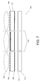
- FIG. 7 depicts a schematic for an array camera module that includes spectral filters disposed proximate the cover glass and in between the cover glass and the optics.
- the array camera module 700 includes optics 702 , spectral filters 708 adjacent to respective cover glasses 710 , and an image sensor 714 including microlenses 712 .
- construction lines 715 are depicted to indicate that the illustrated array camera module can either be a monolithic array camera module or else an array camera module constructed from separate camera modules.
- the aggregate of the cover glass and the spectral filters are coated with anti-reflective coatings 704 , 706 ; specifically, the spectral filters are coated with antireflective coating 704 , and the cover glasses are coated with a second antireflective coating 706 .
- anti-reflective coatings can be implemented to reduce ghosting and enhance general stray light behavior.
- FIG. 7 depicts a spectral filter in between the cover glass and the optics, in many embodiments of the invention, the spectral filter is disposed proximate the cover glass and in between the cover glass and the image sensor.
- the spectral filters are not amenable to being coated with the antireflective coating.
- the antireflective coating may not be able to be sufficiently adjoined to the spectral filters; this can be due to any number of reasons.
- anti-reflective coatings are typically applied using processes such as chemical vapor deposition, evaporation, sputtering, etc., and the color filters may not be able to withstand these processes since the color filters may not be sufficiently stable, even when fully cured (e.g. due to high temperature, ion bombardment, plasma, that may be experienced during the anti-reflective coating application process, etc.).
- FIG. 8 depicts a schematic for an array camera module that includes spectral filters embedded within a cover glass.
- FIG. 8 illustrates an array camera module 800 that includes optics 802 and respective cover glasses 808 that includes embedded spectral filters 806 .
- the array camera module 800 further includes an image sensor 812 that includes microlenses 810 .
- construction lines 815 are depicted to indicate that the illustrated array camera module can either be a monolithic array camera module or else an array camera module constructed from separate camera modules.
- the cover glass 808 is coated with anti-reflective coatings 804 .
- the index of refraction of the spectral filter and cover glass are made to be approximately similar so as to reduce the development of reflections within the glass.
- the color filter has a relatively small thickness so as not to disturb the optomechanical design of the respective camera module.
- the color filter has a thickness of between approximately 0.1 ⁇ m and 1 ⁇ m.
- color filters of any suitable thickness can be implemented. Where a color filter is relatively thicker, the optomechanics of the camera module can be redesigned so as to accommodate the thickness.
- each of the two portions is greater than some threshold thickness.
- each of the two portions has a thickness greater than approximately 200 ⁇ m.
- each of the two portions has a thickness greater than approximately 150 ⁇ m.
- each of the portions has a thickness greater than approximately 100 ⁇ m.
- the thicker portions can facilitate the lamination/gluing processes.
- spectral filters have been depicted and discussed as being disposed proximate or within a cover glass, it should be clear that spectral filters can be disposed within any suitable transparent substrate outside of the image sensor in accordance with embodiments of the invention.
- hybrid spectral filters are implemented within array cameras and/or array camera modules, and this aspect is now discussed in greater detail.
- hybrid infrared cut-off filters (“hybrid IRCF” filters) are implemented within array cameras and array camera modules.
- Hybrid IRCF filters include dielectric infrared cut-off filters (IRCF) and ‘blue glass’ in aggregate.
- IRCF dielectric infrared cut-off filters
- blue glass is a glass that shows spectral absorption in the near infrared (NIR) spectral domain.
- NIR near infrared
- the benefit of combining these two IRCF mechanisms is that due to the absorptive blocking component of the blue glass, the spectral sensitivity of the band edge as well as the dependency on the angle of incidence may not be as strong relative to using a purely dielectric IRCF.
- the dielectric IRCF sharpens the band edge of the filter system over that if only an absorptive filter was used.
- blue glass is used as the substrate material of the dielectric IRCF to build a hybrid IRCF filter.
- the hybrid infrared cut-off filters are disposed within a glass substrate that is outside a constituent image sensor, e.g. similar to the configuration described above.
- FIG. 9 depicts a camera module—that can be implemented within an array camera—that includes a hybrid spectral filter in accordance with an embodiment of the invention.
- the camera module 900 includes optics 902 , a cover glass 908 including an embedded hybrid IRCF filter that includes a dielectric cutoff filter 906 and blue glass 908 in aggregate.
- the cover glass is coated with antireflection coating 910 .
- the camera module further includes an image sensor 912 , including an associated Bayer filter 914 , and microlenses 916 .
- This configuration allows an effective, and environmentally stable, infrared cutoff filter to be implemented within an array camera module.
- a Bayer filter is depicted, any of a variety of filters and filtering arrangements can be implemented in conjunction with the configuration depicted in FIG. 9 .
- a homogenous color filter is implemented within the pixel stack.
- FIG. 9 depicts that additional spectral filters disposed at the image sensor level, it should be clear that the incorporation of a hybrid IRCF filter can be implemented in any of a variety of arrangements.
- an additional spectral filter e.g. a color filter
- an additional spectral filter is disposed elsewhere within the lens stack.
- an additional spectral filter is disposed within the same cover glass as the hybrid spectral filter.
- hybrid IRCF filters can be used in conjunction with any of a variety of arrangements in accordance with embodiments of the invention.
- ‘blue glass’ typically requires some thickness in order to achieve the desired effect.
- the optomechanics of the respective camera module may need to be tailored to accommodate the inclusion of hybrid spectral filters.
- the tailored design of the optomechanics can be mitigated.
- the optical density of the ‘blue glass’ is increased so that it can be effectively implemented in a relatively thinner form factor.
- the glass substrate that includes the hybrid IRCF filter is sealed from the sides, e.g. by resin.
- an array camera module includes at least one camera module that includes a Bayer filter within its image sensor, at least one camera module that includes a hybrid IRCF filter disposed within a cover glass, and/or at least one camera module that includes a color spectral filter (e.g. red, green, or blue) that is disposed within its respective cover glass.
- a color spectral filter e.g. red, green, or blue
Abstract
Description
Claims (18)
Priority Applications (1)
| Application Number | Priority Date | Filing Date | Title |
|---|---|---|---|
| US14/561,925 US9521319B2 (en) | 2014-06-18 | 2014-12-05 | Array cameras and array camera modules including spectral filters disposed outside of a constituent image sensor |
Applications Claiming Priority (2)
| Application Number | Priority Date | Filing Date | Title |
|---|---|---|---|
| US201462014021P | 2014-06-18 | 2014-06-18 | |
| US14/561,925 US9521319B2 (en) | 2014-06-18 | 2014-12-05 | Array cameras and array camera modules including spectral filters disposed outside of a constituent image sensor |
Publications (2)
| Publication Number | Publication Date |
|---|---|
| US20150373261A1 US20150373261A1 (en) | 2015-12-24 |
| US9521319B2 true US9521319B2 (en) | 2016-12-13 |
Family
ID=54870823
Family Applications (1)
| Application Number | Title | Priority Date | Filing Date |
|---|---|---|---|
| US14/561,925 Active US9521319B2 (en) | 2014-06-18 | 2014-12-05 | Array cameras and array camera modules including spectral filters disposed outside of a constituent image sensor |
Country Status (1)
| Country | Link |
|---|---|
| US (1) | US9521319B2 (en) |
Cited By (47)
| Publication number | Priority date | Publication date | Assignee | Title |
|---|---|---|---|---|
| US9706132B2 (en) | 2012-05-01 | 2017-07-11 | Fotonation Cayman Limited | Camera modules patterned with pi filter groups |
| US9712759B2 (en) | 2008-05-20 | 2017-07-18 | Fotonation Cayman Limited | Systems and methods for generating depth maps using a camera arrays incorporating monochrome and color cameras |
| US9743051B2 (en) | 2013-02-24 | 2017-08-22 | Fotonation Cayman Limited | Thin form factor computational array cameras and modular array cameras |
| US9749568B2 (en) | 2012-11-13 | 2017-08-29 | Fotonation Cayman Limited | Systems and methods for array camera focal plane control |
| US9749547B2 (en) | 2008-05-20 | 2017-08-29 | Fotonation Cayman Limited | Capturing and processing of images using camera array incorperating Bayer cameras having different fields of view |
| US9754422B2 (en) | 2012-02-21 | 2017-09-05 | Fotonation Cayman Limited | Systems and method for performing depth based image editing |
| US9774789B2 (en) | 2013-03-08 | 2017-09-26 | Fotonation Cayman Limited | Systems and methods for high dynamic range imaging using array cameras |
| US9794476B2 (en) | 2011-09-19 | 2017-10-17 | Fotonation Cayman Limited | Systems and methods for controlling aliasing in images captured by an array camera for use in super resolution processing using pixel apertures |
| US9800856B2 (en) | 2013-03-13 | 2017-10-24 | Fotonation Cayman Limited | Systems and methods for synthesizing images from image data captured by an array camera using restricted depth of field depth maps in which depth estimation precision varies |
| US9807382B2 (en) | 2012-06-28 | 2017-10-31 | Fotonation Cayman Limited | Systems and methods for detecting defective camera arrays and optic arrays |
| US9811753B2 (en) | 2011-09-28 | 2017-11-07 | Fotonation Cayman Limited | Systems and methods for encoding light field image files |
| US9813616B2 (en) | 2012-08-23 | 2017-11-07 | Fotonation Cayman Limited | Feature based high resolution motion estimation from low resolution images captured using an array source |
| US9858673B2 (en) | 2012-08-21 | 2018-01-02 | Fotonation Cayman Limited | Systems and methods for estimating depth and visibility from a reference viewpoint for pixels in a set of images captured from different viewpoints |
| US9888194B2 (en) | 2013-03-13 | 2018-02-06 | Fotonation Cayman Limited | Array camera architecture implementing quantum film image sensors |
| US9898856B2 (en) | 2013-09-27 | 2018-02-20 | Fotonation Cayman Limited | Systems and methods for depth-assisted perspective distortion correction |
| US9924092B2 (en) | 2013-11-07 | 2018-03-20 | Fotonation Cayman Limited | Array cameras incorporating independently aligned lens stacks |
| US9955070B2 (en) | 2013-03-15 | 2018-04-24 | Fotonation Cayman Limited | Systems and methods for synthesizing high resolution images using image deconvolution based on motion and depth information |
| US9986224B2 (en) | 2013-03-10 | 2018-05-29 | Fotonation Cayman Limited | System and methods for calibration of an array camera |
| US10009538B2 (en) | 2013-02-21 | 2018-06-26 | Fotonation Cayman Limited | Systems and methods for generating compressed light field representation data using captured light fields, array geometry, and parallax information |
| US10091405B2 (en) | 2013-03-14 | 2018-10-02 | Fotonation Cayman Limited | Systems and methods for reducing motion blur in images or video in ultra low light with array cameras |
| US10089740B2 (en) | 2014-03-07 | 2018-10-02 | Fotonation Limited | System and methods for depth regularization and semiautomatic interactive matting using RGB-D images |
| US10122993B2 (en) | 2013-03-15 | 2018-11-06 | Fotonation Limited | Autofocus system for a conventional camera that uses depth information from an array camera |
| US10119808B2 (en) | 2013-11-18 | 2018-11-06 | Fotonation Limited | Systems and methods for estimating depth from projected texture using camera arrays |
| US10127682B2 (en) | 2013-03-13 | 2018-11-13 | Fotonation Limited | System and methods for calibration of an array camera |
| US10182216B2 (en) | 2013-03-15 | 2019-01-15 | Fotonation Limited | Extended color processing on pelican array cameras |
| US10218889B2 (en) | 2011-05-11 | 2019-02-26 | Fotonation Limited | Systems and methods for transmitting and receiving array camera image data |
| US10250871B2 (en) | 2014-09-29 | 2019-04-02 | Fotonation Limited | Systems and methods for dynamic calibration of array cameras |
| US10261219B2 (en) | 2012-06-30 | 2019-04-16 | Fotonation Limited | Systems and methods for manufacturing camera modules using active alignment of lens stack arrays and sensors |
| US10306120B2 (en) | 2009-11-20 | 2019-05-28 | Fotonation Limited | Capturing and processing of images captured by camera arrays incorporating cameras with telephoto and conventional lenses to generate depth maps |
| US10366472B2 (en) | 2010-12-14 | 2019-07-30 | Fotonation Limited | Systems and methods for synthesizing high resolution images using images captured by an array of independently controllable imagers |
| US10390005B2 (en) | 2012-09-28 | 2019-08-20 | Fotonation Limited | Generating images from light fields utilizing virtual viewpoints |
| US10412314B2 (en) | 2013-03-14 | 2019-09-10 | Fotonation Limited | Systems and methods for photometric normalization in array cameras |
| US10455168B2 (en) | 2010-05-12 | 2019-10-22 | Fotonation Limited | Imager array interfaces |
| US10455218B2 (en) | 2013-03-15 | 2019-10-22 | Fotonation Limited | Systems and methods for estimating depth using stereo array cameras |
| US10482618B2 (en) | 2017-08-21 | 2019-11-19 | Fotonation Limited | Systems and methods for hybrid depth regularization |
| US10708492B2 (en) | 2013-11-26 | 2020-07-07 | Fotonation Limited | Array camera configurations incorporating constituent array cameras and constituent cameras |
| US11227405B2 (en) | 2017-06-21 | 2022-01-18 | Apera Ai Inc. | Determining positions and orientations of objects |
| US11270110B2 (en) | 2019-09-17 | 2022-03-08 | Boston Polarimetrics, Inc. | Systems and methods for surface modeling using polarization cues |
| US11290658B1 (en) | 2021-04-15 | 2022-03-29 | Boston Polarimetrics, Inc. | Systems and methods for camera exposure control |
| US11302012B2 (en) | 2019-11-30 | 2022-04-12 | Boston Polarimetrics, Inc. | Systems and methods for transparent object segmentation using polarization cues |
| US11394955B2 (en) * | 2020-01-17 | 2022-07-19 | Aptiv Technologies Limited | Optics device for testing cameras useful on vehicles |
| US11525906B2 (en) | 2019-10-07 | 2022-12-13 | Intrinsic Innovation Llc | Systems and methods for augmentation of sensor systems and imaging systems with polarization |
| US11580667B2 (en) | 2020-01-29 | 2023-02-14 | Intrinsic Innovation Llc | Systems and methods for characterizing object pose detection and measurement systems |
| US11689813B2 (en) | 2021-07-01 | 2023-06-27 | Intrinsic Innovation Llc | Systems and methods for high dynamic range imaging using crossed polarizers |
| US11792538B2 (en) | 2008-05-20 | 2023-10-17 | Adeia Imaging Llc | Capturing and processing of images including occlusions focused on an image sensor by a lens stack array |
| US11797863B2 (en) | 2020-01-30 | 2023-10-24 | Intrinsic Innovation Llc | Systems and methods for synthesizing data for training statistical models on different imaging modalities including polarized images |
| US11954886B2 (en) | 2021-04-15 | 2024-04-09 | Intrinsic Innovation Llc | Systems and methods for six-degree of freedom pose estimation of deformable objects |
Families Citing this family (10)
| Publication number | Priority date | Publication date | Assignee | Title |
|---|---|---|---|---|
| US9106784B2 (en) | 2013-03-13 | 2015-08-11 | Pelican Imaging Corporation | Systems and methods for controlling aliasing in images captured by an array camera for use in super-resolution processing |
| US9215430B2 (en) * | 2013-03-15 | 2015-12-15 | Omnivision Technologies, Inc. | Image sensor with pixels having increased optical crosstalk |
| US9942474B2 (en) | 2015-04-17 | 2018-04-10 | Fotonation Cayman Limited | Systems and methods for performing high speed video capture and depth estimation using array cameras |
| US11089286B2 (en) | 2015-07-29 | 2021-08-10 | Samsung Electronics Co., Ltd. | Image sensor |
| US11469265B2 (en) | 2015-07-29 | 2022-10-11 | Samsung Electronics Co., Ltd. | Imaging apparatus and image sensor including the same |
| US10790325B2 (en) | 2015-07-29 | 2020-09-29 | Samsung Electronics Co., Ltd. | Imaging apparatus and image sensor including the same |
| US10403668B2 (en) * | 2015-07-29 | 2019-09-03 | Samsung Electronics Co., Ltd. | Imaging apparatus and image sensor including the same |
| US11199678B2 (en) * | 2016-09-14 | 2021-12-14 | Fotonation Limited | Optical systems for cameras incorporating lens elements formed separately and subsequently bonded to low CTE substrates |
| US11470287B2 (en) | 2019-12-05 | 2022-10-11 | Samsung Electronics Co., Ltd. | Color imaging apparatus using monochrome sensors for mobile devices |
| IL273118B (en) | 2020-03-05 | 2022-03-01 | Allen Richter | Self-adaptive electromagnetic energy attenuator |
Citations (533)
| Publication number | Priority date | Publication date | Assignee | Title |
|---|---|---|---|---|
| US4124798A (en) | 1965-12-09 | 1978-11-07 | Thompson Kenneth B | Optical viewing apparatus |
| US4198646A (en) | 1978-10-13 | 1980-04-15 | Hughes Aircraft Company | Monolithic imager for near-IR |
| US4323925A (en) | 1980-07-07 | 1982-04-06 | Avco Everett Research Laboratory, Inc. | Method and apparatus for arraying image sensor modules |
| JPS5925483U (en) | 1982-08-09 | 1984-02-17 | 住友電気工業株式会社 | Defective insulator detection device |
| US4460449A (en) | 1983-01-03 | 1984-07-17 | Amerace Corporation | Apparatus for making a tool |
| US4467365A (en) | 1980-10-16 | 1984-08-21 | Fuji Xerox Co., Ltd. | Control system for reading device |
| JPS6437177U (en) | 1987-08-31 | 1989-03-06 | ||
| JPH02285772A (en) | 1989-04-26 | 1990-11-26 | Toshiba Corp | Picture reader |
| US5005083A (en) | 1988-05-19 | 1991-04-02 | Siemens Aktiengesellschaft | FLIR system with two optical channels for observing a wide and a narrow field of view |
| US5070414A (en) | 1988-09-20 | 1991-12-03 | Kabushiki Kaisha Toshiba | Method and apparatus for reading image information formed on material |
| US5144448A (en) | 1990-07-31 | 1992-09-01 | Vidar Systems Corporation | Scanning apparatus using multiple CCD arrays and related method |
| US5327125A (en) | 1992-07-13 | 1994-07-05 | Sharp Kabushiki Kaisha | Apparatus for and method of converting a sampling frequency according to a data driven type processing |
| US5629524A (en) | 1995-02-21 | 1997-05-13 | Advanced Scientific Concepts, Inc. | High speed crystallography detector |
| EP0840502A2 (en) | 1996-11-04 | 1998-05-06 | Eastman Kodak Company | Compact digital camera with segmented fields of view |
| US5808350A (en) | 1997-01-03 | 1998-09-15 | Raytheon Company | Integrated IR, visible and NIR sensor and methods of fabricating same |
| US5832312A (en) | 1996-02-22 | 1998-11-03 | Eastman Kodak Company | Watertight body for accommodating a photographic camera |
| US5880691A (en) | 1995-11-07 | 1999-03-09 | California Institute Of Technology | Capacitively coupled successive approximation ultra low power analog-to-digital converter |
| JPH11142609A (en) | 1997-11-14 | 1999-05-28 | Nikon Corp | Production of diffusion plate and diffusion plate as well as production of microlens array and microlens array |
| US5933190A (en) | 1995-04-18 | 1999-08-03 | Imec Vzw | Pixel structure, image sensor using such pixel structure and corresponding peripheral circuitry |
| JPH11223708A (en) | 1998-02-09 | 1999-08-17 | Nikon Corp | Indentator and production of micro-optical element array |
| US5973844A (en) | 1996-01-26 | 1999-10-26 | Proxemics | Lenslet array systems and methods |
| US6002743A (en) | 1996-07-17 | 1999-12-14 | Telymonde; Timothy D. | Method and apparatus for image acquisition from a plurality of cameras |
| US6005607A (en) | 1995-06-29 | 1999-12-21 | Matsushita Electric Industrial Co., Ltd. | Stereoscopic computer graphics image generating apparatus and stereoscopic TV apparatus |
| US6034690A (en) | 1996-08-02 | 2000-03-07 | U.S. Philips Corporation | Post-processing generation of focus/defocus effects for computer graphics images |
| US6069365A (en) | 1997-11-25 | 2000-05-30 | Alan Y. Chow | Optical processor based imaging system |
| US6069351A (en) | 1998-07-16 | 2000-05-30 | Intel Corporation | Focal plane processor for scaling information from image sensors |
| JP2000209503A (en) | 1999-01-19 | 2000-07-28 | Nippon Hoso Kyokai <Nhk> | Solid state image pickup device and its video signal output device |
| US6097394A (en) | 1997-04-28 | 2000-08-01 | Board Of Trustees, Leland Stanford, Jr. University | Method and system for light field rendering |
| US6124974A (en) | 1996-01-26 | 2000-09-26 | Proxemics | Lenslet array systems and methods |
| US6141048A (en) | 1996-08-19 | 2000-10-31 | Eastman Kodak Company | Compact image capture device |
| US6160909A (en) | 1998-04-01 | 2000-12-12 | Canon Kabushiki Kaisha | Depth control for stereoscopic images |
| US6163414A (en) | 1997-10-20 | 2000-12-19 | Fuji Xerox Co., Ltd. | Image reading apparatus |
| US6172352B1 (en) | 1998-03-20 | 2001-01-09 | Syscan, Inc. | Sensing module for accelerating signal readout from image sensors |
| US6205241B1 (en) | 1998-06-01 | 2001-03-20 | Canon Kabushiki Kaisha | Compression of stereoscopic images |
| US6239909B1 (en) | 1997-12-25 | 2001-05-29 | Olympus Optical Co. Ltd. | Image-forming method and image-forming apparatus |
| US20010005225A1 (en) | 1997-07-24 | 2001-06-28 | Vincent S. Clark | Focal plane exposure control system for cmos area image sensors |
| US20010019621A1 (en) | 1998-08-28 | 2001-09-06 | Hanna Keith James | Method and apparatus for processing images |
| JP2001277260A (en) | 2000-03-30 | 2001-10-09 | Seiko Epson Corp | Micro-lens array, its production method, and original board and display for producing it |
| US20010038387A1 (en) | 1999-11-30 | 2001-11-08 | Takatoshi Tomooka | Image display method, image display system, host device, image display device and display interface |
| US20020012056A1 (en) | 1999-02-26 | 2002-01-31 | Roy T. Trevino | Light sensor with increased dynamic range |
| US20020027608A1 (en) | 1998-09-23 | 2002-03-07 | Honeywell, Inc. | Method and apparatus for calibrating a tiled display |
| US6358862B1 (en) | 1999-09-02 | 2002-03-19 | Micron Technology, Inc | Passivation integrity improvements |
| US20020039438A1 (en) | 1996-02-21 | 2002-04-04 | Katsuhiko Mori | Matching point extracting method and apparatus therefor |
| EP1201407A2 (en) | 2000-10-31 | 2002-05-02 | Eastman Kodak Company | Method of manufacturing a microlens array mold and a microlens array |
| US20020063807A1 (en) | 1999-04-19 | 2002-05-30 | Neal Margulis | Method for Performing Image Transforms in a Digital Display System |
| US20020087403A1 (en) | 2001-01-03 | 2002-07-04 | Nokia Corporation | Statistical metering and filtering of content via pixel-based metadata |
| JP2002195910A (en) | 2000-12-26 | 2002-07-10 | Omron Corp | System for testing optical part |
| US20020089596A1 (en) | 2000-12-28 | 2002-07-11 | Yasuo Suda | Image sensing apparatus |
| US20020094027A1 (en) | 2001-01-15 | 2002-07-18 | Noriyuki Sato | Transmission header compressor not compressing transmission headers attached to intra-frame coded moving-picture data |
| US20020101528A1 (en) | 1998-01-22 | 2002-08-01 | Paul P. Lee | Integrated cmos active pixel digital camera |
| US20020113867A1 (en) | 1997-02-20 | 2002-08-22 | Tomoshi Takigawa | Stereoscopic image display apparatus for detecting viewpoint position and forming stereoscopic image while following up viewpoint position |
| US20020113888A1 (en) | 2000-12-18 | 2002-08-22 | Kazuhiro Sonoda | Image pickup apparatus |
| US6477260B1 (en) | 1998-11-02 | 2002-11-05 | Nissan Motor Co., Ltd. | Position measuring apparatus using a pair of electronic cameras |
| US6476805B1 (en) | 1999-12-23 | 2002-11-05 | Microsoft Corporation | Techniques for spatial displacement estimation and multi-resolution operations on light fields |
| US20020163054A1 (en) | 2001-03-21 | 2002-11-07 | Yasuo Suda | Semiconductor device and its manufacture method |
| US20020167537A1 (en) | 2001-05-11 | 2002-11-14 | Miroslav Trajkovic | Motion-based tracking with pan-tilt-zoom camera |
| US20020177054A1 (en) | 2001-04-24 | 2002-11-28 | Kenji Saitoh | Exposure method and apparatus |
| US6502097B1 (en) | 1999-12-23 | 2002-12-31 | Microsoft Corporation | Data structure for efficient access to variable-size data objects |
| US20030025227A1 (en) | 2001-08-02 | 2003-02-06 | Zograph, Llc | Reproduction of relief patterns |
| US6525302B2 (en) | 2001-06-06 | 2003-02-25 | The Regents Of The University Of Colorado | Wavefront coding phase contrast imaging systems |
| JP2003094445A (en) | 2001-09-20 | 2003-04-03 | Seiko Epson Corp | Manufacturing method for fine structure, manufacturing method for device equipped with the fine structure, fine structure by the manufacturing method, device for manufacturing the fine structure, and device for manufacturing device equipped with the fine structure |
| US20030086079A1 (en) | 2001-10-31 | 2003-05-08 | Lfk-Lenkflugkoerpersysteme Gmbh | Process and apparatus for automatically determining the modulation transfer function of focal plane array cameras |
| US6563537B1 (en) | 1997-07-31 | 2003-05-13 | Fuji Photo Film Co., Ltd. | Image signal interpolation |
| JP2003139910A (en) | 2001-10-30 | 2003-05-14 | Sony Corp | Optical element, method and device for manufacturing the same, and liquid crystal display device and image projection type display device using the same |
| US6571466B1 (en) | 2000-03-27 | 2003-06-03 | Amkor Technology, Inc. | Flip chip image sensor package fabrication method |
| JP2003163938A (en) | 2001-11-28 | 2003-06-06 | Japan Science & Technology Corp | Image-input apparatus |
| US20030124763A1 (en) | 2001-05-30 | 2003-07-03 | Taiwan Semiconductor Manufacturing Company | Colors only process to reduce package yield loss |
| US20030140347A1 (en) | 1999-12-22 | 2003-07-24 | Viktor Varsa | Method for transmitting video images, a data transmission system, a transmitting video terminal, and a receiving video terminal |
| US6603513B1 (en) | 1999-02-16 | 2003-08-05 | Micron Technology, Inc. | Using a single control line to provide select and reset signals to image sensors in two rows of a digital imaging device |
| US6611289B1 (en) | 1999-01-15 | 2003-08-26 | Yanbin Yu | Digital cameras using multiple sensors with multiple lenses |
| US20030179418A1 (en) | 2002-03-19 | 2003-09-25 | Eastman Kodak Company | Producing a defective pixel map from defective cluster pixels in an area array image sensor |
| US6628330B1 (en) | 1999-09-01 | 2003-09-30 | Neomagic Corp. | Color interpolator and horizontal/vertical edge enhancer using two line buffer and alternating even/odd filters for digital camera |
| US6627896B1 (en) | 1999-07-27 | 2003-09-30 | Canon Kabushiki Kaisha | Image sensing apparatus |
| US6639596B1 (en) | 1999-09-20 | 2003-10-28 | Microsoft Corporation | Stereo reconstruction from multiperspective panoramas |
| US20030211405A1 (en) | 2002-05-13 | 2003-11-13 | Kartik Venkataraman | Color filter imaging array and method of formation |
| US6657218B2 (en) | 2000-11-01 | 2003-12-02 | Seiko Epson Corporation | Method and apparatus for measuring gap, method and apparatus for measuring shape and method for manufacturing liquid crystal device |
| US6671399B1 (en) | 1999-10-27 | 2003-12-30 | Canon Kabushiki Kaisha | Fast epipolar line adjustment of stereo pairs |
| US20040008271A1 (en) | 2002-07-04 | 2004-01-15 | Minolta Co., Ltd. | Imaging device and digital camera using the imaging device |
| US20040012689A1 (en) | 2002-07-16 | 2004-01-22 | Fairchild Imaging | Charge coupled devices in tiled arrays |
| US20040027358A1 (en) | 2002-08-09 | 2004-02-12 | Hayato Nakao | Image data generating apparatus |
| US20040047274A1 (en) | 2002-06-27 | 2004-03-11 | Olumpus Optical Co., Ltd. | Image pickup lens unit and image pickup device |
| US20040050104A1 (en) | 2002-09-18 | 2004-03-18 | Eastman Kodak Company | Forming information transfer lens array |
| US20040056966A1 (en) | 2000-07-21 | 2004-03-25 | Schechner Yoav Y. | Method and apparatus for image mosaicing |
| US20040061787A1 (en) | 2002-09-30 | 2004-04-01 | Zicheng Liu | Foveated wide-angle imaging system and method for capturing and viewing wide-angle images in real time |
| US20040066454A1 (en) | 2002-07-03 | 2004-04-08 | Topcon Corporation | Device and method of measuring data for calibration, program for measuring data for calibration, program recording medium readable with computer, and image data processing device |
| US20040100570A1 (en) | 2002-11-19 | 2004-05-27 | Makoto Shizukuishi | Image sensor and digital camera |
| US20040105021A1 (en) | 2002-12-02 | 2004-06-03 | Bolymedia Holdings Co., Ltd. | Color filter patterns for image sensors |
| US6750904B1 (en) | 1998-10-31 | 2004-06-15 | International Business Machines Corporation | Camera system for three dimensional images and video |
| US20040114807A1 (en) | 2002-12-13 | 2004-06-17 | Dan Lelescu | Statistical representation and coding of light field data |
| US6765617B1 (en) | 1997-11-14 | 2004-07-20 | Tangen Reidar E | Optoelectronic camera and method for image formatting in the same |
| US6771833B1 (en) | 1999-08-20 | 2004-08-03 | Eastman Kodak Company | Method and system for enhancing digital images |
| US20040151401A1 (en) | 2000-12-01 | 2004-08-05 | Sawhney Harpreet S. | Techniques and systems for developing high-resolution imagery |
| JP2004221585A (en) | 2003-01-09 | 2004-08-05 | Dialog Semiconductor | Aps pixel provided with capability of reset noise suppression and programable binning |
| US6774941B1 (en) | 1999-10-26 | 2004-08-10 | National Semiconductor Corporation | CCD output processing stage that amplifies signals from colored pixels based on the conversion efficiency of the colored pixels |
| US20040165090A1 (en) | 2003-02-13 | 2004-08-26 | Alex Ning | Auto-focus (AF) lens and process |
| US20040169617A1 (en) | 2003-03-01 | 2004-09-02 | The Boeing Company | Systems and methods for providing enhanced vision imaging with decreased latency |
| US20040170340A1 (en) | 2003-02-27 | 2004-09-02 | Microsoft Corporation | Bayesian image super resolution |
| US20040174439A1 (en) | 2003-03-07 | 2004-09-09 | Upton Wayne A. | High frame rate high definition imaging system and method |
| US20040179834A1 (en) | 2003-03-14 | 2004-09-16 | Eastman Kodak Company | Camera using beam splitter with micro-lens image amplification |
| US6795253B2 (en) | 2002-05-08 | 2004-09-21 | Fuji Photo Optical Co., Ltd. | Imaging lens |
| US20040207836A1 (en) | 2002-09-27 | 2004-10-21 | Rajeshwar Chhibber | High dynamic range optical inspection system and method |
| US20040213449A1 (en) | 2003-02-03 | 2004-10-28 | Photon Dynamics, Inc. | Method and apparatus for optical inspection of a display |
| US20040218809A1 (en) | 2003-05-02 | 2004-11-04 | Microsoft Corporation | Cyclopean virtual imaging via generalized probabilistic smoothing |
| US6819358B1 (en) | 1999-04-26 | 2004-11-16 | Microsoft Corporation | Error calibration for digital image sensors and apparatus using the same |
| US20040240052A1 (en) | 2003-06-02 | 2004-12-02 | Pentax Corporation | Multiple-focal imaging device, and a mobile device having the multiple-focal-length imaging device |
| US20040251509A1 (en) | 2003-06-11 | 2004-12-16 | Choi Kyoung-Sei | CMOS type image sensor module having transparent polymeric encapsulation material |
| US20040264806A1 (en) | 2003-06-24 | 2004-12-30 | Microsoft Corporation | System and method for de-noising multiple copies of a signal |
| US20050006477A1 (en) | 2003-07-07 | 2005-01-13 | Mehul Patel | Imaging arrangement and barcode imager for imaging an optical code or target at a plurality of focal planes |
| US20050009313A1 (en) | 2003-06-06 | 2005-01-13 | Sanyo Electric Co., Ltd. | Manufacturing method for semiconductor device |
| US20050012035A1 (en) | 2003-01-21 | 2005-01-20 | Miller Steven D. | System and method for significant dust detection and enhancement of dust images over land and ocean |
| US20050036778A1 (en) | 2003-08-12 | 2005-02-17 | Demonte Frank J. | Fixed-focus camera module and associated method of assembly |
| US20050047678A1 (en) | 2003-09-03 | 2005-03-03 | Jones James L. | Image change detection systems, methods, and articles of manufacture |
| US20050048690A1 (en) | 2003-06-24 | 2005-03-03 | Katsumi Yamamoto | Image sensor having micro-lens array separated with trench structures and method of making |
| US20050068436A1 (en) | 2001-05-29 | 2005-03-31 | Miriam Fraenkel | CMOS imager for cellular applications and methods of using such |
| US6879735B1 (en) | 1998-09-14 | 2005-04-12 | University Of Utah Reasearch Foundation | Method of digital image enhancement and sharpening |
| JP2005116022A (en) | 2003-10-06 | 2005-04-28 | Toshiba Corp | Method and apparatus for manufacturing magnetic recording medium, imprint stamper, and manufacturing method therefor |
| US6903770B1 (en) | 1998-07-27 | 2005-06-07 | Sanyo Electric Co., Ltd. | Digital camera which produces a single image based on two exposures |
| US20050128595A1 (en) | 2003-12-16 | 2005-06-16 | Nobuo Shimizu | Substrate with recess portion for microlens, microlens substrate, transmissive screen, rear type projector, and method of manufacturing substrate with recess portion for microlens |
| US20050132098A1 (en) | 2003-12-11 | 2005-06-16 | Canon Kabushiki Kaisha | Relay apparatus for relaying communication from CPU to peripheral device |
| US6909121B2 (en) | 1998-05-11 | 2005-06-21 | Seiko Epson Corporation | Microlens array substrate, method of manufacturing the same, and display device |
| US20050134712A1 (en) | 2003-12-18 | 2005-06-23 | Gruhlke Russell W. | Color image sensor having imaging element array forming images on respective regions of sensor elements |
| US20050147277A1 (en) | 2004-01-05 | 2005-07-07 | Honda Motor Co., Ltd | Apparatus, method and program for moving object detection |
| US20050151759A1 (en) | 2003-09-08 | 2005-07-14 | Gonzalez-Banos Hector H. | Systems and methods for directly generating a view using a layered approach |
| US6927922B2 (en) | 2001-12-18 | 2005-08-09 | The University Of Rochester | Imaging using a multifocal aspheric lens to obtain extended depth of field |
| US20050175257A1 (en) | 2002-05-21 | 2005-08-11 | Yoshihiko Kuroki | Information processing apparatus, information processing system, and dialogist displaying method |
| US20050185711A1 (en) | 2004-02-20 | 2005-08-25 | Hanspeter Pfister | 3D television system and method |
| US20050205785A1 (en) | 2001-05-11 | 2005-09-22 | Bert Hornback | Imaging device with multiple fields of view incorporating memory-based temperature compensation of an uncooled focal plane array |
| US20050219363A1 (en) | 2004-04-05 | 2005-10-06 | Kohler Timothy L | Imaging device analysis systems and imaging device analysis methods |
| US20050225654A1 (en) | 2004-04-08 | 2005-10-13 | Digital Optics Corporation | Thin color camera |
| JP2005295381A (en) | 2004-04-02 | 2005-10-20 | Sony Corp | Imaging apparatus |
| US6958862B1 (en) | 2003-04-21 | 2005-10-25 | Foveon, Inc. | Use of a lenslet array with a vertically stacked pixel array |
| US20050275946A1 (en) | 2004-05-19 | 2005-12-15 | The Regents Of The University Of California | Optical system applicable to improving the dynamic range of Shack-Hartmann sensors |
| US20050286612A1 (en) | 2004-06-28 | 2005-12-29 | Nec Electronics Corporation | De-interleaver, mobile communication terminal, and de-interleaving method |
| US20050286756A1 (en) | 2004-06-25 | 2005-12-29 | Stmicroelectronics, Inc. | Segment based image matching method and system |
| US20060002635A1 (en) | 2004-06-30 | 2006-01-05 | Oscar Nestares | Computing a higher resolution image from multiple lower resolution images using model-based, robust bayesian estimation |
| US20060023314A1 (en) | 2004-07-27 | 2006-02-02 | Boettiger Ulrich C | Controlling lens shape in a microlens array |
| JP2006033493A (en) | 2004-07-16 | 2006-02-02 | Matsushita Electric Ind Co Ltd | Imaging apparatus |
| US20060023197A1 (en) | 2004-07-27 | 2006-02-02 | Joel Andrew H | Method and system for automated production of autostereoscopic and animated prints and transparencies from digital and non-digital media |
| US20060028476A1 (en) | 2004-08-03 | 2006-02-09 | Irwin Sobel | Method and system for providing extensive coverage of an object using virtual cameras |
| US20060035415A1 (en) * | 2004-08-16 | 2006-02-16 | Wood Alan G | Frame structure and semiconductor attach process for use therewith for fabrication of image sensor packages and the like, and resulting packages |
| JP2006047944A (en) | 2004-03-24 | 2006-02-16 | Fuji Photo Film Co Ltd | Photographing lens |
| US20060034003A1 (en) | 2004-08-16 | 2006-02-16 | Xceed Imaging Ltd. | Optical method and system for extended depth of focus |
| US20060033005A1 (en) | 2004-08-11 | 2006-02-16 | Dmitri Jerdev | Correction of non-uniform sensitivity in an image array |
| US20060038891A1 (en) | 2003-01-31 | 2006-02-23 | Masatoshi Okutomi | Method for creating high resolution color image, system for creating high resolution color image and program creating high resolution color image |
| US20060046204A1 (en) * | 2004-08-31 | 2006-03-02 | Sharp Laboratories Of America, Inc. | Directly patternable microlens |
| US20060049930A1 (en) | 2002-07-15 | 2006-03-09 | Levi Zruya | Method and apparatus for implementing multipurpose monitoring system |
| US20060054780A1 (en) | 2004-09-15 | 2006-03-16 | Raytheon Company | Multispectral imaging chip using photonic crystals |
| US20060055811A1 (en) | 2004-09-14 | 2006-03-16 | Frtiz Bernard S | Imaging system having modules with adaptive optical elements |
| US20060054782A1 (en) | 2004-08-25 | 2006-03-16 | Olsen Richard I | Apparatus for multiple camera devices and method of operating same |
| US7015954B1 (en) | 1999-08-09 | 2006-03-21 | Fuji Xerox Co., Ltd. | Automatic video system using multiple cameras |
| US20060069478A1 (en) | 2004-09-30 | 2006-03-30 | Clarion Co., Ltd. | Parking-assist system using image information from an imaging camera and distance information from an infrared laser camera |
| US20060072029A1 (en) | 2002-10-25 | 2006-04-06 | Konica Minolta Holdings, Inc. | Image input device |
| US20060087747A1 (en) | 2004-10-21 | 2006-04-27 | Konica Minolta Opto. Inc. | Optical system, image pickup device and digital apparatus |
| US20060098888A1 (en) | 2004-10-22 | 2006-05-11 | Nikon Corporation | Imaging device and image processing program for estimating fixed pattern noise from partial noise output of available pixel area |
| US20060125936A1 (en) | 2004-12-15 | 2006-06-15 | Gruhike Russell W | Multi-lens imaging systems and methods |
| US20060138322A1 (en) | 2003-01-31 | 2006-06-29 | Costello Kenneth A | Backside imaging through a doped layer |
| US20060152803A1 (en) | 2005-01-11 | 2006-07-13 | Provitola Anthony I | Enhancement of depth perception |
| US20060159369A1 (en) | 2005-01-19 | 2006-07-20 | U.S. Army Research Laboratory | Method of super-resolving images |
| US20060157640A1 (en) | 2005-01-18 | 2006-07-20 | Perlman Stephen G | Apparatus and method for capturing still images and video using coded aperture techniques |
| US7085409B2 (en) | 2000-10-18 | 2006-08-01 | Sarnoff Corporation | Method and apparatus for synthesizing new video and/or still imagery from a collection of real video and/or still imagery |
| US20060187338A1 (en) | 2005-02-18 | 2006-08-24 | May Michael J | Camera phone using multiple lenses and image sensors to provide an extended zoom range |
| US20060197937A1 (en) | 2005-02-08 | 2006-09-07 | Canesta, Inc. | Methods and system to quantify depth data accuracy in three-dimensional sensors using single frame capture |
| US20060203113A1 (en) | 2003-02-21 | 2006-09-14 | Takamasa Wada | Solid-state image pickup device and drive method thereof |
| US20060210186A1 (en) | 1999-12-10 | 2006-09-21 | Kathrin Berkner | Multiscale sharpening and smoothing with wavelets |
| JP2006258930A (en) | 2005-03-15 | 2006-09-28 | Nikon Corp | Method for manufacturing microlens and method for manufacturing die for microlens |
| US20060239549A1 (en) | 2005-04-26 | 2006-10-26 | Kelly Sean C | Method and apparatus for correcting a channel dependent color aberration in a digital image |
| US20060243889A1 (en) | 2004-07-19 | 2006-11-02 | Farnworth Warren M | Microelectronic imagers with optical devices and methods of manufacturing such microelectronic imagers |
| US20060251410A1 (en) | 2005-05-05 | 2006-11-09 | Trutna William R Jr | Imaging device employing optical motion sensor as gyroscope |
| US20060274174A1 (en) | 2005-06-02 | 2006-12-07 | Tewinkle Scott L | System for controlling integration times of photosensors in an imaging device |
| US20060278948A1 (en) | 2005-06-08 | 2006-12-14 | Matsushita Electric Industrial Co., Ltd. | Solid-state image sensor and manufacturing method thereof |
| US20060279648A1 (en) | 2005-06-09 | 2006-12-14 | Fuji Photo Film Co., Ltd. | Imaging device and digital camera |
| EP1734766A2 (en) | 2005-06-14 | 2006-12-20 | Samsung Electronics Co., Ltd. | Transport stream structure including image data and apparatus and method for transmitting and receiving image data |
| US20070002159A1 (en) | 2005-07-01 | 2007-01-04 | Olsen Richard I | Method and apparatus for use in camera and systems employing same |
| US7161614B1 (en) | 1999-11-26 | 2007-01-09 | Sanyo Electric Co., Ltd. | Device and method for converting two-dimensional video to three-dimensional video |
| US20070024614A1 (en) | 2005-07-26 | 2007-02-01 | Tam Wa J | Generating a depth map from a two-dimensional source image for stereoscopic and multiview imaging |
| US20070036427A1 (en) | 2005-08-15 | 2007-02-15 | Makibi Nakamura | Depth information for auto focus using two pictures and two-dimensional gaussian scale space theory |
| US20070040922A1 (en) | 2005-08-22 | 2007-02-22 | Micron Technology, Inc. | HDR/AB on multi-way shared pixels |
| US20070040828A1 (en) | 2003-05-13 | 2007-02-22 | Eceed Imaging Ltd. | Optical method and system for enhancing image resolution |
| US20070041391A1 (en) | 2005-08-18 | 2007-02-22 | Micron Technology, Inc. | Method and apparatus for controlling imager output data rate |
| US20070052825A1 (en) | 2000-08-07 | 2007-03-08 | Kwang-Bo Cho | Pixel optimization for color |
| US20070083114A1 (en) | 2005-08-26 | 2007-04-12 | The University Of Connecticut | Systems and methods for image resolution enhancement |
| US20070085917A1 (en) | 2005-10-14 | 2007-04-19 | Fujifilm Corporation | Image pickup apparatus for preventing linearity defect |
| US20070126898A1 (en) | 2004-09-27 | 2007-06-07 | Digital Optics Corporation | Thin camera and associated methods |
| US20070127831A1 (en) | 2003-04-10 | 2007-06-07 | Kartik Venkataraman | Compression system for integrated sensor devices |
| US20070139333A1 (en) | 2004-08-26 | 2007-06-21 | Susumu Sato | Optical element |
| US20070146511A1 (en) | 2005-11-17 | 2007-06-28 | Sony Corporation | Signal processing apparatus for solid-state imaging device, signal processing method, and imaging system |
| US20070159541A1 (en) | 2006-01-09 | 2007-07-12 | Sparks Andrew W | Single camera multi-spectral imager |
| US20070158427A1 (en) | 2003-11-13 | 2007-07-12 | Xiaoxun Zhu | Method of automatically reading code symbols on objects present within the field of view (FOV) of a hand-supportable digital-imaging based code symbol reader, by simultaneously projecting an image cropping zone (ICZ) framing pattern and a field of illumination within the FOV during object illuminationand imaging operations |
| US20070160310A1 (en) | 2003-12-01 | 2007-07-12 | Japan Science And Technology Agency | Apparatus and method for image configuring |
| JP2007520107A (en) | 2003-12-18 | 2007-07-19 | アバゴ・テクノロジーズ・ジェネラル・アイピー(シンガポール)プライベート・リミテッド | Color image sensor having an image sensor for forming an image on each area of the sensor element |
| US20070165931A1 (en) | 2005-12-07 | 2007-07-19 | Honda Motor Co., Ltd. | Human being detection apparatus, method of detecting human being, and human being detecting program |
| WO2007083579A1 (en) | 2006-01-20 | 2007-07-26 | Matsushita Electric Industrial Co., Ltd. | Compound eye camera module and method of producing the same |
| US20070171290A1 (en) | 2003-05-08 | 2007-07-26 | Ronald Kroger | Pixel patterns |
| CN101010619A (en) | 2004-08-26 | 2007-08-01 | 财团法人秋田企业活性化中心 | Optical element |
| US20070182843A1 (en) * | 2006-02-03 | 2007-08-09 | Fujifilm Corporation | Solid-state imaging device and electronic endoscope using the same |
| US7262799B2 (en) | 2000-10-25 | 2007-08-28 | Canon Kabushiki Kaisha | Image sensing apparatus and its control method, control program, and storage medium |
| US20070206241A1 (en) | 2006-03-06 | 2007-09-06 | Micron Technology, Inc. | Fused multi-array color image sensor |
| US20070211164A1 (en) | 2004-08-25 | 2007-09-13 | Olsen Richard I | Imager module optical focus and assembly method |
| US20070216765A1 (en) | 2006-03-16 | 2007-09-20 | Wong Earl Q | Simple method for calculating camera defocus from an image scene |
| US20070228256A1 (en) | 2006-03-31 | 2007-10-04 | Mentzer Ray A | Analog vertical sub-sampling in an active pixel sensor (APS) image sensor |
| US7292735B2 (en) | 2004-04-16 | 2007-11-06 | Microsoft Corporation | Virtual image artifact detection |
| US20070258006A1 (en) | 2005-08-25 | 2007-11-08 | Olsen Richard I | Solid state camera optics frame and assembly |
| US20070258706A1 (en) | 2006-05-08 | 2007-11-08 | Ramesh Raskar | Method for deblurring images using optimized temporal coding patterns |
| US20070257184A1 (en) | 2005-08-25 | 2007-11-08 | Olsen Richard I | Large dynamic range cameras |
| US7295697B1 (en) | 1999-12-06 | 2007-11-13 | Canon Kabushiki Kaisha | Depth information measurement apparatus and mixed reality presentation system |
| US20070263114A1 (en) | 2006-05-01 | 2007-11-15 | Microalign Technologies, Inc. | Ultra-thin digital imaging device of high resolution for mobile electronic devices and method of imaging |
| US20070268374A1 (en) | 2006-05-12 | 2007-11-22 | Robinson M D | End-to-end design of superresolution electro-optic imaging systems |
| US20070296847A1 (en) | 2006-06-21 | 2007-12-27 | Chao-Chi Chang | Method of making image capture unit |
| US20070296832A1 (en) | 2006-06-12 | 2007-12-27 | Masataka Ota | Imaging apparatus |
| US20070296835A1 (en) | 2005-08-25 | 2007-12-27 | Olsen Richard I | Digital cameras with direct luminance and chrominance detection |
| US20080006859A1 (en) * | 2006-06-19 | 2008-01-10 | Stmicroelectronics Rousset Sas | Method for manufacturing lenses, in particular for an imager comprising a diaphragm |
| US20080019611A1 (en) | 2004-03-31 | 2008-01-24 | Canon Kabushiki Kaisha | Imaging System Performance Measurement |
| US20080025649A1 (en) | 2002-02-07 | 2008-01-31 | Microsoft Coporation | Transformation of exif images |
| US20080043096A1 (en) | 2006-04-04 | 2008-02-21 | Anthony Vetro | Method and System for Decoding and Displaying 3D Light Fields |
| US20080043095A1 (en) | 2006-04-04 | 2008-02-21 | Anthony Vetro | Method and System for Acquiring, Encoding, Decoding and Displaying 3D Light Fields |
| JP2008039852A (en) | 2006-08-01 | 2008-02-21 | Agc Techno Glass Co Ltd | Glass optical element and its manufacturing method |
| US20080054518A1 (en) | 2006-08-31 | 2008-03-06 | Samsung Electro-Mechanics Co., Ltd. | Method of manufacturing a stamper |
| JP2008507874A (en) | 2004-07-23 | 2008-03-13 | ザ サイエンス アンド テクノロジー ファシリティーズ カウンシル | Imaging device |
| US20080062164A1 (en) | 2006-08-11 | 2008-03-13 | Bassi Zorawar | System and method for automated calibration and correction of display geometry and color |
| US20080080028A1 (en) | 2006-10-02 | 2008-04-03 | Micron Technology, Inc. | Imaging method, apparatus and system having extended depth of field |
| US20080079805A1 (en) | 2006-09-29 | 2008-04-03 | Ayako Takagi | Stereoscopic image display apparatus and stereoscopic image producing method |
| US20080084486A1 (en) | 2006-10-04 | 2008-04-10 | Enge Amy D | Providing multiple video signals from single sensor |
| US20080088793A1 (en) | 2006-09-25 | 2008-04-17 | Sverdrup Lawrence H | Methods and lenses for correction of chromatic aberration |
| US20080095523A1 (en) | 2006-10-18 | 2008-04-24 | Lynn Schilling-Benz | Lens array assisted focus detection |
| US20080099804A1 (en) * | 2006-10-26 | 2008-05-01 | Omnivision Technologies, Inc. | Image sensor having curved micro-mirrors over the sensing photodiode and method for fabricating |
| US7369165B2 (en) | 2001-08-31 | 2008-05-06 | Stmicroelectronics S.R.L. | Noise filter for Bayer pattern image data |
| US20080112635A1 (en) | 2006-11-15 | 2008-05-15 | Sony Corporation | Imaging apparatus and method, and method for designing imaging apparatus |
| US20080112059A1 (en) | 2006-11-13 | 2008-05-15 | Samsung Electronics Co., Ltd. | Optical lens and method of manufacturing the same |
| US20080118241A1 (en) | 2006-11-16 | 2008-05-22 | Tekolste Robert | Control of stray light in camera systems employing an optics stack and associated methods |
| US20080131019A1 (en) | 2006-12-01 | 2008-06-05 | Yi-Ren Ng | Interactive Refocusing of Electronic Images |
| US20080131107A1 (en) | 2006-12-01 | 2008-06-05 | Fujifilm Corporation | Photographing apparatus |
| US7391572B2 (en) | 2006-03-01 | 2008-06-24 | International Business Machines Corporation | Hybrid optical/electronic structures fabricated by a common molding process |
| US20080151097A1 (en) | 2006-12-22 | 2008-06-26 | Industrial Technology Research Institute | Autofocus searching method |
| US20080152215A1 (en) | 2006-12-26 | 2008-06-26 | Kenichi Horie | Coding method, electronic camera, recording medium storing coded program, and decoding method |
| US20080152296A1 (en) | 2006-12-21 | 2008-06-26 | Byung Tae Oh | Methods and Systems for Processing Film Grain Noise |
| US20080158375A1 (en) | 2006-12-29 | 2008-07-03 | Nokia Corporation | Method and system for image pre-processing |
| US20080158259A1 (en) | 2006-12-28 | 2008-07-03 | Texas Instruments Incorporated | Image warping and lateral color correction |
| US20080158698A1 (en) | 2006-12-29 | 2008-07-03 | Chao-Chi Chang | Lens barrel array and lens array and the method of making the same |
| US7408725B2 (en) | 2005-09-29 | 2008-08-05 | Fujinon Corporation | Single focus lens |
| US20080187305A1 (en) | 2007-02-06 | 2008-08-07 | Ramesh Raskar | 4D light field cameras |
| US20080193026A1 (en) | 2007-02-09 | 2008-08-14 | Kenichi Horie | Decoding method, decoding apparatus, storage medium in which decoding program is stored, and electronic camera |
| US20080219654A1 (en) | 2007-03-09 | 2008-09-11 | Border John N | Camera using multiple lenses and image sensors to provide improved focusing capability |
| US20080218610A1 (en) | 2005-09-30 | 2008-09-11 | Glenn Harrison Chapman | Methods and Apparatus for Detecting Defects in Imaging Arrays by Image Analysis |
| WO2008108271A1 (en) | 2007-03-06 | 2008-09-12 | Sharp Kabushiki Kaisha | Imaging lens, imaging unit and portable information terminal provided with the imaging unit |
| WO2008108926A1 (en) | 2007-03-07 | 2008-09-12 | Altasens, Inc. | Apparatus and method for reducing edge effect in an image sensor |
| US7425984B2 (en) | 2003-04-04 | 2008-09-16 | Stmicroelectronics, Inc. | Compound camera and methods for implementing auto-focus, depth-of-field and high-resolution functions |
| US20080240598A1 (en) | 2007-03-30 | 2008-10-02 | Brother Kogyo Kabushiki Kaisha | Image processor |
| US20080239116A1 (en) | 2007-03-27 | 2008-10-02 | Micron Technology, Inc. | Method and apparatus for automatic linear shift parallax correction for multi-array image systems |
| US20080247653A1 (en) | 2007-04-03 | 2008-10-09 | Micron Technology, Inc. | Method and apparatus for parallelization of image compression encoders |
| US20080247638A1 (en) | 2007-03-26 | 2008-10-09 | Funai Electric Co., Ltd. | Three-Dimensional Object Imaging Device |
| JP2008258885A (en) | 2007-04-04 | 2008-10-23 | Texas Instr Japan Ltd | Imaging apparatus and driving method of imaging apparatus |
| US20080273751A1 (en) | 2006-10-16 | 2008-11-06 | Chang Yuan | Detection and Tracking of Moving Objects from a Moving Platform in Presence of Strong Parallax |
| US20080272416A1 (en) | 2007-05-03 | 2008-11-06 | Young Je Yun | Image sensor and method of manufacturing the same |
| US20080278591A1 (en) | 2007-05-09 | 2008-11-13 | Barna Sandor L | Method and apparatus for improving low-light performance for small pixel image sensors |
| US20080298674A1 (en) | 2007-05-29 | 2008-12-04 | Image Masters Inc. | Stereoscopic Panoramic imaging system |
| WO2008150817A1 (en) | 2007-05-31 | 2008-12-11 | Artificial Muscle, Inc. | Optical systems employing compliant electroactive materials |
| US20090052743A1 (en) | 2004-10-12 | 2009-02-26 | Axel Techmer | Motion estimation in a plurality of temporally successive digital images |
| US20090050946A1 (en) | 2004-07-25 | 2009-02-26 | Jacques Duparre | Camera module, array based thereon, and method for the production thereof |
| US20090060281A1 (en) | 2007-03-26 | 2009-03-05 | Funai Electric Co., Ltd. | Object Distance Deriving Device |
| US20090086074A1 (en) | 2007-09-27 | 2009-04-02 | Omnivision Technologies, Inc. | Dual mode camera solution apparatus, system, and method |
| US20090091806A1 (en) | 2007-10-09 | 2009-04-09 | Masafumi Inuiya | Solid-state imaging device, imaging apparatus, and method for manufacturing solid-state imaging device |
| US20090096050A1 (en) | 2007-10-11 | 2009-04-16 | Park Seung Ryong | Image Sensor and Method for Manufacturing the Same |
| US20090102956A1 (en) | 2007-10-18 | 2009-04-23 | Georgiev Todor G | Fast Computational Camera Based On Two Arrays of Lenses |
| US20090109306A1 (en) | 2007-10-26 | 2009-04-30 | Jizhang Shan | High dynamic range sensor with reduced line memory for color interpolation |
| US20090128833A1 (en) | 2007-11-15 | 2009-05-21 | Giora Yahav | Dual mode depth imaging |
| US20090129667A1 (en) | 2007-11-16 | 2009-05-21 | Gwangju Institute Of Science And Technology | Device and method for estimatiming depth map, and method for generating intermediate image and method for encoding multi-view video using the same |
| US20090140131A1 (en) | 2005-06-23 | 2009-06-04 | Nikon Corporation | Image input apparatus, photodetection apparatus, and image synthesis method |
| US20090152664A1 (en) | 2007-04-18 | 2009-06-18 | Ethan Jacob Dukenfield Klem | Materials, Systems and Methods for Optoelectronic Devices |
| JP2009132010A (en) | 2007-11-29 | 2009-06-18 | Panasonic Electric Works Co Ltd | Manufacturing method of mold for microlens array |
| US20090167922A1 (en) | 2005-01-18 | 2009-07-02 | Perlman Stephen G | Apparatus and method for capturing still images and video using coded lens imaging techniques |
| US20090180021A1 (en) | 2008-01-15 | 2009-07-16 | Fujifilm Corporation | Method for adjusting position of image sensor, method and apparatus for manufacturing a camera module, and camera module |
| US20090179142A1 (en) | 2006-01-23 | 2009-07-16 | Jacques Duparre | Image Detection System and Method For Production at Least One Image Detection System |
| US20090201371A1 (en) | 2005-03-23 | 2009-08-13 | Panasonic Corporation | On-vehicle imaging device |
| US20090200622A1 (en) | 2008-02-11 | 2009-08-13 | Omnivision Technologies, Inc. | Self-aligned filter for an image sensor |
| US20090207235A1 (en) | 2005-11-30 | 2009-08-20 | Gianluca Francini | Method for Determining Scattered Disparity Fields in Stereo Vision |
| US20090219435A1 (en) * | 2008-02-29 | 2009-09-03 | Hon Hai Precision Industry Co., Ltd. | Composite lens and lens module having same |
| US20090225203A1 (en) | 2008-02-28 | 2009-09-10 | Funai Electric Co., Ltd. | Compound-eye imaging device |
| TW200939739A (en) | 2007-10-23 | 2009-09-16 | Aptina Imaging Corp | Methods, systems and apparatuses using barrier self-calibration for high dynamic range imagers |
| EP2104334A1 (en) | 2006-12-04 | 2009-09-23 | Sony Corporation | Imaging device and imaging method |
| US20090237520A1 (en) | 2003-07-18 | 2009-09-24 | Katsumi Kaneko | Image pick-up appararus and synchronization-signal-generating apparatus |
| US20090245573A1 (en) | 2008-03-03 | 2009-10-01 | Videolq, Inc. | Object matching for tracking, indexing, and search |
| US7606484B1 (en) | 2006-03-23 | 2009-10-20 | Flir Systems, Inc. | Infrared and near-infrared camera hyperframing |
| US20090263017A1 (en) | 2002-10-10 | 2009-10-22 | Anthony Amir Tanbakuchi | Method for reconstruction of pixel color values |
| US20090268983A1 (en) | 2005-07-25 | 2009-10-29 | The Regents Of The University Of California | Digital imaging system and method using multiple digital image sensors to produce large high-resolution gapless mosaic images |
| US20090268970A1 (en) | 2008-04-29 | 2009-10-29 | Sevket Derin Babacan | Method and Apparatus for Block-Based Compression of Light-field Images |
| US20090268192A1 (en) | 2008-04-25 | 2009-10-29 | Rockwell Collins, Inc. | High dynamic range sensor system and method |
| US20090274387A1 (en) | 2008-05-05 | 2009-11-05 | Micron Technology, Inc. | Method of capturing high dynamic range images with objects in the scene |
| US20090284651A1 (en) | 2008-05-19 | 2009-11-19 | Microsoft Corporation | Quantization and differential coding of alpha image data |
| US20090297056A1 (en) | 2008-05-28 | 2009-12-03 | Micron Technology, Inc. | Method and apparatus for extended depth-of-field image restoration |
| US20090302205A9 (en) | 2004-08-25 | 2009-12-10 | Olsen Richard I | Lens frame and optical focus assembly for imager module |
| US7633511B2 (en) | 2004-04-01 | 2009-12-15 | Microsoft Corporation | Pop-up light field |
| CN101606086A (en) | 2006-10-11 | 2009-12-16 | 珀莱特公司 | Be used to prepare the method for adjustable lens |
| WO2009151903A2 (en) | 2008-05-20 | 2009-12-17 | Pelican Imaging Corporation | Capturing and processing of images using monolithic camera array with hetergeneous imagers |
| US7639435B2 (en) | 2007-04-04 | 2009-12-29 | Hon Hai Precision Industry Co., Ltd. | Optical module with adhesively mounted filter |
| WO2009157273A1 (en) | 2008-06-25 | 2009-12-30 | コニカミノルタオプト株式会社 | Imaging optical system, and imaging lens manufacturing method |
| US20090323195A1 (en) | 2008-06-27 | 2009-12-31 | Micron Technology, Inc. | Lens master devices, lens structures, imaging devices, and methods and apparatuses of making the same |
| US20090324118A1 (en) | 2008-06-30 | 2009-12-31 | Oleg Maslov | Computing higher resolution images from multiple lower resolution images |
| US20090323206A1 (en) | 2008-06-25 | 2009-12-31 | Micron Technology, Inc. | Imaging module with symmetrical lens system and method of manufacture |
| US20100002314A1 (en) | 2008-07-01 | 2010-01-07 | Micron Technology, Inc. | Lens system with symmetrical optics |
| US20100002126A1 (en) | 2004-11-16 | 2010-01-07 | Aptina Imaging Corporation | System and method for focusing a digital camera |
| US20100002313A1 (en) | 2008-07-02 | 2010-01-07 | Jacques Duparre | Method and apparatus providing singlet wafer lens system with field flattener |
| US7646549B2 (en) | 2006-12-18 | 2010-01-12 | Xceed Imaging Ltd | Imaging system and method for providing extended depth of focus, range extraction and super resolved imaging |
| US20100013927A1 (en) | 2008-04-11 | 2010-01-21 | Nearmap Pty Ltd. | Systems and Methods of Capturing Large Area Images in Detail Including Cascaded Cameras and/or Calibration Features |
| US7657090B2 (en) | 2003-05-26 | 2010-02-02 | Noritsu Koki Co., Ltd. | Region detecting method and region detecting apparatus |
| US20100044815A1 (en) * | 2008-08-20 | 2010-02-25 | Hon Hai Precision Industry Co., Ltd. | Cmos image sensor package and camera module using same |
| US20100053600A1 (en) | 2008-09-01 | 2010-03-04 | Funai Electric Co., Ltd. | Optical Condition Design Method for a Compound-Eye Imaging Device |
| US20100053342A1 (en) | 2008-09-04 | 2010-03-04 | Samsung Electronics Co. Ltd. | Image edit method and apparatus for mobile terminal |
| US7675681B2 (en) | 2007-02-02 | 2010-03-09 | Toshiba Matsushita Display Technology Co., Ltd. | Display device |
| US7675080B2 (en) | 2006-01-10 | 2010-03-09 | Aptina Imaging Corp. | Uniform color filter arrays in a moat |
| US20100060746A9 (en) | 2004-08-25 | 2010-03-11 | Richard Ian Olsen | Simultaneous multiple field of view digital cameras |
| US20100074532A1 (en) | 2006-11-21 | 2010-03-25 | Mantisvision Ltd. | 3d geometric modeling and 3d video content creation |
| US20100073463A1 (en) | 2008-09-25 | 2010-03-25 | Kabushiki Kaisha Toshiba | Stereoscopic image capturing apparatus and stereoscopic image capturing system |
| US20100086227A1 (en) | 2008-10-04 | 2010-04-08 | Microsoft Corporation | Image super-resolution using gradient profile prior |
| US20100085425A1 (en) | 2008-10-07 | 2010-04-08 | Kar-Han Tan | One-Touch Projector Alignment for 3D Stereo Display |
| US20100091389A1 (en) | 2006-10-11 | 2010-04-15 | Polight As | Design of compact adjustable lens |
| US20100097491A1 (en) | 2008-10-21 | 2010-04-22 | Stmicroelectronics S.R.L. | Compound camera sensor and related method of processing digital images |
| US7706634B2 (en) | 2003-01-20 | 2010-04-27 | Fraunhofer-Gesellschaft Zur Foerderung Der Angewandten Forschung E.V. | Method and camera (apparatus) for optically capturing a screen |
| US20100103308A1 (en) | 2008-10-29 | 2010-04-29 | Jabil Circuit, Inc. | Positioning wafer lenses on electronic imagers |
| US20100103259A1 (en) | 2008-10-20 | 2010-04-29 | Funai Electric Co., Ltd. | Object Distance Deriving Device |
| US20100111444A1 (en) | 2007-04-24 | 2010-05-06 | Coffman Thayne R | Method and system for fast dense stereoscopic ranging |
| US20100118127A1 (en) | 2008-11-13 | 2010-05-13 | Samsung Electronics Co., Ltd. | Wide depth of field 3D display apparatus and method |
| US7723662B2 (en) | 2005-10-07 | 2010-05-25 | The Board Of Trustees Of The Leland Stanford Junior University | Microscopy arrangements and approaches |
| US20100133418A1 (en) | 2005-01-07 | 2010-06-03 | Edward Sargent | Quantum dot optical devices with enhanced gain and sensitivity and methods of making same |
| US20100142839A1 (en) | 2008-11-19 | 2010-06-10 | Canon Kabushiki Kaisha | Dvc as generic file format for plenoptic camera |
| US20100141802A1 (en) | 2008-12-08 | 2010-06-10 | Timothy Knight | Light Field Data Acquisition Devices, and Methods of Using and Manufacturing Same |
| US20100157073A1 (en) | 2008-12-22 | 2010-06-24 | Yuhi Kondo | Image processing apparatus, image processing method, and program |
| US20100165152A1 (en) | 2008-12-30 | 2010-07-01 | Massachusetts Institute Of Technology | Processing Images Having Different Focus |
| US20100166410A1 (en) | 2008-12-27 | 2010-07-01 | Hon Hai Precision Industry Co., Ltd. | Camera module array for obtaining compound images |
| US20100177411A1 (en) | 2009-01-09 | 2010-07-15 | Shashikant Hegde | Wafer level lens replication on micro-electrical-mechanical systems |
| US20100195716A1 (en) | 2007-06-26 | 2010-08-05 | Koninklijke Philips Electronics N.V. | Method and system for encoding a 3d video signal, enclosed 3d video signal, method and system for decoder for a 3d video signal |
| US20100194901A1 (en) | 2009-02-02 | 2010-08-05 | L-3 Communications Cincinnati Electronics Corporation | Multi-Channel Imaging Devices |
| US20100202054A1 (en) | 2007-08-11 | 2010-08-12 | David Niederer | Liquid Lens System |
| US20100201834A1 (en) | 2009-02-10 | 2010-08-12 | Sony Corporation | Solid-state imaging device, method of manufacturing the same, and electronic apparatus |
| US7782364B2 (en) | 2007-08-21 | 2010-08-24 | Aptina Imaging Corporation | Multi-array sensor with integrated sub-array for parallax detection and photometer functionality |
| US20100231285A1 (en) | 2009-03-12 | 2010-09-16 | Boomer James B | Mipi analog switch for automatic selection of multiple image sensors |
| US20100244165A1 (en) | 2009-03-26 | 2010-09-30 | Micron Technology, Inc. | Method and apparatus providing combined spacer and optical lens element |
| US20100265385A1 (en) | 2009-04-18 | 2010-10-21 | Knight Timothy J | Light Field Camera Image, File and Configuration Data, and Methods of Using, Storing and Communicating Same |
| US20100265381A1 (en) | 2009-04-16 | 2010-10-21 | Sony Corporation | Imaging device |
| US7826153B2 (en) | 2006-11-24 | 2010-11-02 | Lg Innotek Co., Ltd. | Lens assembly and method for manufacturing the same |
| US20100281070A1 (en) | 2009-05-01 | 2010-11-04 | Creative Technology Ltd | Data file having more than one mode of operation |
| US7840067B2 (en) | 2003-10-24 | 2010-11-23 | Arcsoft, Inc. | Color matching and color correction for images forming a panoramic image |
| US20100302423A1 (en) | 2009-05-27 | 2010-12-02 | Adams Jr James E | Four-channel color filter array pattern |
| US20100309292A1 (en) | 2007-11-29 | 2010-12-09 | Gwangju Institute Of Science And Technology | Method and apparatus for generating multi-viewpoint depth map, method for generating disparity of multi-viewpoint image |
| US20100309368A1 (en) * | 2009-06-03 | 2010-12-09 | Samsung Electronics Co., Ltd. | Wafer-level lens module and image pickup module including the same |
| US20100321595A1 (en) | 2009-06-18 | 2010-12-23 | Hon Hai Precision Industry Co., Ltd. | Camera module with liquid crystal module |
| US20110001037A1 (en) | 2009-07-02 | 2011-01-06 | Xerox Corporation | Image sensor with integration time compensation |
| WO2011008443A2 (en) | 2009-06-29 | 2011-01-20 | Lensvector Inc. | Wafer level camera module with active optical element |
| US20110018973A1 (en) | 2008-03-26 | 2011-01-27 | Konica Minolta Holdings, Inc. | Three-dimensional imaging device and method for calibrating three-dimensional imaging device |
| US20110019243A1 (en) | 2009-07-21 | 2011-01-27 | Constant Jr Henry J | Stereoscopic form reader |
| JP2011017764A (en) | 2009-07-07 | 2011-01-27 | Konica Minolta Opto Inc | Imaging lens, imaging apparatus and portable terminal |
| US20110032370A1 (en) | 2008-05-25 | 2011-02-10 | Avistar Communications Corporation | Synthetic image formation signal processing hardware for vignetted optoelectronic arrays, lensless cameras, and integrated camera-displays |
| US20110031381A1 (en) * | 2007-12-28 | 2011-02-10 | Hiok-Nam Tay | Light guide array for an image sensor |
| US20110043661A1 (en) | 2008-02-08 | 2011-02-24 | University Of Kent | Camera Adapter Based Optical Imaging Apparatus |
| US20110044502A1 (en) | 2009-04-28 | 2011-02-24 | Hisense State Key Laboratory Of Digital Multi-Media Technology Co., Ltd. | Motion detection method, apparatus and system |
| US20110043668A1 (en) | 2009-08-24 | 2011-02-24 | Mckinnon Patrick R | Detection of Defective Pixels in an Image Sensor |
| US20110043665A1 (en) | 2009-08-19 | 2011-02-24 | Kabushiki Kaisha Toshiba | Image processing device, solid-state imaging device, and camera module |
| US20110051255A1 (en) | 2009-08-31 | 2011-03-03 | Samsung Electronics Co., Ltd. | Fluidic lens and method of manufacturing the same |
| US7912673B2 (en) | 2005-03-11 | 2011-03-22 | Creaform Inc. | Auto-referenced system and apparatus for three-dimensional scanning |
| US20110080487A1 (en) | 2008-05-20 | 2011-04-07 | Pelican Imaging Corporation | Capturing and processing of images using monolithic camera array with heterogeneous imagers |
| WO2011055655A1 (en) | 2009-11-05 | 2011-05-12 | コニカミノルタオプト株式会社 | Image pickup device, optical unit, wafer lens laminated body, and method for manufacturing wafer lens laminated body |
| WO2011063347A2 (en) | 2009-11-20 | 2011-05-26 | Pelican Imaging Corporation | Capturing and processing of images using monolithic camera array with heterogeneous imagers |
| US20110121421A1 (en) | 2008-05-09 | 2011-05-26 | Ecole Polytechnique Federate de Lausanne EPFL | Image sensor having nonlinear response |
| US20110128412A1 (en) | 2009-11-25 | 2011-06-02 | Milnes Thomas B | Actively Addressable Aperture Light Field Camera |
| US20110128393A1 (en) | 2009-12-01 | 2011-06-02 | Nokia Corporation | Digital imaging |
| JP2011109484A (en) | 2009-11-18 | 2011-06-02 | Sharp Corp | Multi-lens camera apparatus and electronic information device |
| EP2336816A2 (en) | 2009-12-04 | 2011-06-22 | Ricoh Company, Ltd. | Imaging device |
| US20110149408A1 (en) | 2006-09-21 | 2011-06-23 | Sinvent As | Compact polymer lens |
| US20110153248A1 (en) | 2009-12-23 | 2011-06-23 | Yeming Gu | Ophthalmic quality metric system |
| US20110157321A1 (en) | 2009-12-25 | 2011-06-30 | Casio Computer Co., Ltd. | Imaging device, 3d modeling data creation method, and computer-readable recording medium storing programs |
| US7973834B2 (en) | 2007-09-24 | 2011-07-05 | Jianwen Yang | Electro-optical foveated imaging and tracking system |
| US20110176020A1 (en) | 2010-01-20 | 2011-07-21 | Hon Hai Precision Industry Co., Ltd. | Camera module with lens array |
| US7986018B2 (en) | 2006-10-23 | 2011-07-26 | Sony Corporation | Solid-state imaging device |
| US20110181797A1 (en) | 2008-09-01 | 2011-07-28 | Lensvector Inc. | Wafer-level fabrication of liquid crystal optoelectronic devices |
| US7990447B2 (en) | 2006-06-14 | 2011-08-02 | Kabushiki Kaisha Toshiba | Solid-state image sensor |
| US8000498B2 (en) | 2007-12-21 | 2011-08-16 | Industrial Research Institute | Moving object detection apparatus and method |
| KR20110097647A (en) | 2010-02-23 | 2011-08-31 | 삼성전자주식회사 | Apparatus and method for generating a three-dimension image data in portable terminal |
| US20110211824A1 (en) | 2008-01-23 | 2011-09-01 | Georgiev Todor G | Methods and Apparatus for Full-Resolution Light-Field Capture and Rendering |
| US8013904B2 (en) | 2008-12-09 | 2011-09-06 | Seiko Epson Corporation | View projection matrix based high performance low latency display pipeline |
| US20110221599A1 (en) | 2010-03-09 | 2011-09-15 | Flir Systems, Inc. | Imager with multiple sensor arrays |
| US20110221950A1 (en) | 2010-03-12 | 2011-09-15 | Doeke Jolt Oostra | Camera device, wafer scale package |
| US20110221939A1 (en) | 2005-08-03 | 2011-09-15 | Dmitri Jerdev | Correction of cluster defects in imagers |
| US20110221658A1 (en) | 2010-02-28 | 2011-09-15 | Osterhout Group, Inc. | Augmented reality eyepiece with waveguide having a mirrored surface |
| US20110228144A1 (en) * | 2010-03-19 | 2011-09-22 | Hui Tian | Dark current reduction in image sensors via dynamic electrical biasing |
| WO2011116203A1 (en) | 2010-03-17 | 2011-09-22 | Pelican Imaging Corporation | Fabrication process for mastering imaging lens arrays |
| US8027531B2 (en) | 2004-07-21 | 2011-09-27 | The Board Of Trustees Of The Leland Stanford Junior University | Apparatus and method for capturing a scene using staggered triggering of dense camera arrays |
| US20110234841A1 (en) | 2009-04-18 | 2011-09-29 | Lytro, Inc. | Storage and Transmission of Pictures Including Multiple Frames |
| US20110242342A1 (en) | 2010-04-05 | 2011-10-06 | Qualcomm Incorporated | Combining data from multiple image sensors |
| US20110255745A1 (en) | 2008-11-14 | 2011-10-20 | The Scripps Research Institute | Image analysis platform for identifying artifacts in samples and laboratory consumables |
| US20110255592A1 (en) | 2008-10-27 | 2011-10-20 | Lg Electronics Inc. | Virtual view image synthesis method and apparatus |
| US20110261993A1 (en) | 2010-04-26 | 2011-10-27 | City University Of Hong Kong | Well focused catadioptric image acquisition |
| US20110267348A1 (en) | 2010-04-29 | 2011-11-03 | Dennis Lin | Systems and methods for generating a virtual camera viewpoint for an image |
| US20110273531A1 (en) | 2009-12-14 | 2011-11-10 | Atsushi Ito | Image processing apparatus, image processing method and program |
| US20110274366A1 (en) | 2010-05-07 | 2011-11-10 | Microsoft Corporation | Depth map confidence filtering |
| WO2011143501A1 (en) | 2010-05-12 | 2011-11-17 | Pelican Imaging Corporation | Architectures for imager arrays and array cameras |
| US20110285866A1 (en) | 2010-05-18 | 2011-11-24 | Satish Kumar Bhrugumalla | Multi-Channel Imager |
| US20110300929A1 (en) | 2010-06-03 | 2011-12-08 | Microsoft Corporation | Synthesis of information from multiple audiovisual sources |
| US20110298917A1 (en) | 2010-03-19 | 2011-12-08 | Satoshi Yanagita | Imaging apparatus, method, program, and recording medium used in the program |
| US8077245B2 (en) | 2004-03-17 | 2011-12-13 | Adamo Thomas J | Apparatus for imaging using an array of lenses |
| US20110310980A1 (en) | 2010-06-22 | 2011-12-22 | Qualcomm Mems Technologies, Inc. | Apparatus and methods for processing frames of video data across a display interface using a block-based encoding scheme and a tag id |
| US20110317766A1 (en) | 2010-06-25 | 2011-12-29 | Gwangju Institute Of Science And Technology | Apparatus and method of depth coding using prediction mode |
| US8098297B2 (en) | 2008-09-03 | 2012-01-17 | Sony Corporation | Pre- and post-shutter signal image capture and sort for digital camera |
| US8098304B2 (en) | 2003-07-07 | 2012-01-17 | Zoran Corporation | Dynamic identification and correction of defective pixels |
| US8106949B2 (en) | 2009-03-26 | 2012-01-31 | Seiko Epson Corporation | Small memory footprint light transport matrix capture |
| US20120026342A1 (en) | 2010-07-27 | 2012-02-02 | Xiaoguang Yu | Electronic system communicating with image sensor |
| US20120026451A1 (en) | 2010-07-29 | 2012-02-02 | Lensvector Inc. | Tunable liquid crystal lens with single sided contacts |
| US20120026297A1 (en) | 2009-03-30 | 2012-02-02 | Shunichi Sato | Imaging apparatus and imaging method |
| US20120039525A1 (en) | 2010-08-12 | 2012-02-16 | At&T Intellectual Property I, L.P. | Apparatus and method for providing three dimensional media content |
| US20120044249A1 (en) | 2002-03-27 | 2012-02-23 | Sanyo Electric Co., Ltd. | Method and apparatus for processing three-dimensional images |
| US20120044372A1 (en) | 2010-08-18 | 2012-02-23 | Apple Inc. | Dual image sensor image processing system and method |
| US8126279B2 (en) | 2007-11-19 | 2012-02-28 | The University Of Arizona | Lifting-based view compensated compression and remote visualization of volume rendered images |
| US8130120B2 (en) | 2007-02-27 | 2012-03-06 | Toyota Jidosha Kabushiki Kaisha | Parking assistance device |
| US20120062702A1 (en) | 2010-09-09 | 2012-03-15 | Qualcomm Incorporated | Online reference generation and tracking for multi-user augmented reality |
| US20120069235A1 (en) | 2010-09-20 | 2012-03-22 | Canon Kabushiki Kaisha | Image capture with focus adjustment |
| US8164629B1 (en) | 2003-02-12 | 2012-04-24 | The Research Foundation Of State University Of New York | Linear system based, qualitative independent motion detection from compressed mpeg surveillance video |
| US8169486B2 (en) | 2006-06-05 | 2012-05-01 | DigitalOptics Corporation Europe Limited | Image acquisition method and apparatus |
| US20120105691A1 (en) | 2010-11-03 | 2012-05-03 | Sony Corporation | Lens and colour filter arrangement, super-resolution camera system and method |
| WO2012057622A1 (en) | 2010-10-24 | 2012-05-03 | Ziv Attar | System and method for imaging using multi aperture camera |
| US20120113413A1 (en) | 2009-08-11 | 2012-05-10 | Ether Precision, Inc | Method and device for algining a lens with an optical system |
| US20120113318A1 (en) | 2010-11-04 | 2012-05-10 | Lensvector Inc. | Methods of Adjustment Free Manufacture Of Focus Free Camera Modules |
| US8180145B2 (en) | 2007-12-28 | 2012-05-15 | Industrial Technology Research Institute | Method for producing image with depth by using 2D images |
| US8189089B1 (en) | 2009-01-20 | 2012-05-29 | Adobe Systems Incorporated | Methods and apparatus for reducing plenoptic camera artifacts |
| US8189065B2 (en) | 2008-01-23 | 2012-05-29 | Adobe Systems Incorporated | Methods and apparatus for full-resolution light-field capture and rendering |
| WO2012074361A1 (en) | 2010-12-03 | 2012-06-07 | Mimos Berhad | Method of image segmentation using intensity and depth information |
| US20120147205A1 (en) | 2010-12-14 | 2012-06-14 | Pelican Imaging Corporation | Systems and methods for synthesizing high resolution images using super-resolution processes |
| WO2012078126A1 (en) | 2010-12-08 | 2012-06-14 | Thomson Licensing | System and method for trinocular depth acquisition with triangular sensor |
| US20120147139A1 (en) | 2010-03-19 | 2012-06-14 | Bo Li | Stereoscopic image aligning apparatus, stereoscopic image aligning method, and program of the same |
| US20120153153A1 (en) | 2007-07-25 | 2012-06-21 | Eminent Electronic Technology Corp. | Integrated Ambient Light Sensor and Distance Sensor |
| US20120154551A1 (en) | 2010-12-17 | 2012-06-21 | Canon Kabushiki Kaisha | Stereo image display system, stereo imaging apparatus and stereo display apparatus |
| US20120163672A1 (en) | 2010-12-22 | 2012-06-28 | David Mckinnon | Depth Estimate Determination, Systems and Methods |
| US8212914B2 (en) | 2009-07-24 | 2012-07-03 | Hon Hai Precision Industry Co., Ltd. | Computational imaging system |
| US8213711B2 (en) | 2007-04-03 | 2012-07-03 | Her Majesty The Queen In Right Of Canada As Represented By The Minister Of Industry, Through The Communications Research Centre Canada | Method and graphical user interface for modifying depth maps |
| US20120170134A1 (en) | 2009-09-15 | 2012-07-05 | Commissariat A L'energie Atomique Et Aux Ene Alt | Optical device with deformable piezoelectric actuation membrane |
| US20120169433A1 (en) | 2010-12-30 | 2012-07-05 | Apple Inc. | Digital signal filter |
| US20120176479A1 (en) | 2002-11-21 | 2012-07-12 | Vision Iii Imaging, Inc. | Critical Alignment of Parallax Images for Autostereoscopic Display |
| US20120188420A1 (en) | 2011-01-25 | 2012-07-26 | Black Robert A | Imaging systems with array cameras for depth sensing |
| US20120188389A1 (en) | 2011-01-25 | 2012-07-26 | Peng Lin | Method and apparatus for parallax correction in fused array imaging systems |
| US20120188634A1 (en) | 2011-01-20 | 2012-07-26 | Kenneth Scott Kubala | Passively Athermalized Infrared Imaging System And Method Of Manufacturing Same |
| US20120200734A1 (en) | 2011-02-09 | 2012-08-09 | Research In Motion Limited | Increased low light sensitivity for image sensors by combining quantum dot sensitivity to visible and infrared light |
| US8244058B1 (en) | 2008-05-30 | 2012-08-14 | Adobe Systems Incorporated | Method and apparatus for managing artifacts in frequency domain processing of light-field images |
| US8244027B2 (en) | 2008-01-25 | 2012-08-14 | Fuji Jukogyo Kabushiki Kaisha | Vehicle environment recognition system |
| US8242426B2 (en) | 2006-12-12 | 2012-08-14 | Dolby Laboratories Licensing Corporation | Electronic camera having multiple sensors for capturing high dynamic range images and related methods |
| US20120229628A1 (en) | 2009-11-13 | 2012-09-13 | Eiji Ishiyama | Distance measuring apparatus, distance measuring method, distance measuring program, distance measuring system, and image pickup apparatus |
| US8280194B2 (en) | 2008-04-29 | 2012-10-02 | Sony Corporation | Reduced hardware implementation for a two-picture depth map algorithm |
| US8279325B2 (en) | 2008-11-25 | 2012-10-02 | Lytro, Inc. | System and method for acquiring, editing, generating and outputting video data |
| US20120249836A1 (en) | 2011-03-28 | 2012-10-04 | Sony Corporation | Method and apparatus for performing user inspired visual effects rendering on an image |
| US20120249550A1 (en) | 2009-04-18 | 2012-10-04 | Lytro, Inc. | Selective Transmission of Image Data Based on Device Attributes |
| US20120249750A1 (en) | 2009-12-15 | 2012-10-04 | Thomson Licensing | Stereo-image quality and disparity/depth indications |
| US8290358B1 (en) | 2007-06-25 | 2012-10-16 | Adobe Systems Incorporated | Methods and apparatus for light-field imaging |
| US20120262607A1 (en) | 2009-12-24 | 2012-10-18 | Tomoya Shimura | Multocular image pickup apparatus and multocular image pickup method |
| US8294099B2 (en) | 2009-04-10 | 2012-10-23 | Bae Systems Information And Electronic Systems Integration Inc. | On-wafer butted microbolometer imaging array |
| US20120268574A1 (en) | 2011-04-22 | 2012-10-25 | Commissariat A L'energie Atomique Et Aux Ene Alt | Imager integrated circuit and stereoscopic image capture device |
| US8305456B1 (en) | 2011-05-11 | 2012-11-06 | Pelican Imaging Corporation | Systems and methods for transmitting and receiving array camera image data |
| US8315476B1 (en) | 2009-01-20 | 2012-11-20 | Adobe Systems Incorporated | Super-resolution with the focused plenoptic camera |
| US20120293695A1 (en) | 2011-02-28 | 2012-11-22 | Seiji Tanaka | Color imaging apparatus |
| US20120307099A1 (en) * | 2011-05-30 | 2012-12-06 | Canon Kabushiki Kaisha | Image processing apparatus, image processing method and program |
| US8345144B1 (en) | 2009-07-15 | 2013-01-01 | Adobe Systems Incorporated | Methods and apparatus for rich image capture with focused plenoptic cameras |
| WO2013003276A1 (en) | 2011-06-28 | 2013-01-03 | Pelican Imaging Corporation | Optical arrangements for use with an array camera |
| US20130002828A1 (en) | 2011-07-01 | 2013-01-03 | Yuanyuan Ding | Context and Epsilon Stereo Constrained Correspondence Matching |
| US20130010073A1 (en) | 2011-07-08 | 2013-01-10 | Do Minh N | System and method for generating a depth map and fusing images from a camera array |
| US20130016885A1 (en) | 2011-07-14 | 2013-01-17 | Canon Kabushiki Kaisha | Image processing apparatus, imaging system, and image processing system |
| US20130022111A1 (en) | 2011-07-22 | 2013-01-24 | Qualcomm Incorporated | Coding motion depth maps with depth range variation |
| US8360574B2 (en) | 2006-03-20 | 2013-01-29 | High Performance Optics, Inc. | High performance selective light wavelength filtering providing improved contrast sensitivity |
| US20130033585A1 (en) | 2011-08-04 | 2013-02-07 | Aptina Imaging Corporation | Systems and methods for color compensation in multi-view video |
| US20130033579A1 (en) | 2010-02-19 | 2013-02-07 | Dual Aperture Inc. | Processing multi-aperture image data |
| US20130050504A1 (en) | 2011-08-29 | 2013-02-28 | Qualcomm Incorporated | Fast calibration of displays using spectral-based colorimetrically calibrated multicolor camera |
| US20130050526A1 (en) | 2011-08-24 | 2013-02-28 | Brian Keelan | Super-resolution imaging systems |
| US8400555B1 (en) | 2009-12-01 | 2013-03-19 | Adobe Systems Incorporated | Focused plenoptic camera employing microlenses with different focal lengths |
| US20130070060A1 (en) | 2011-09-19 | 2013-03-21 | Pelican Imaging Corporation | Systems and methods for determining depth from multiple views of a scene that include aliasing using hypothesized fusion |
| US20130077880A1 (en) | 2011-09-28 | 2013-03-28 | Pelican Imaging Corporation | Systems and methods for encoding light field image files |
| US20130076967A1 (en) | 2011-09-28 | 2013-03-28 | Apple Inc. | Dynamic Autofocus Opertions |
| US20130088637A1 (en) | 2011-10-11 | 2013-04-11 | Pelican Imaging Corporation | Lens Stack Arrays Including Adaptive Optical Elements |
| US20130088489A1 (en) | 2010-06-29 | 2013-04-11 | Koninklijke Philips Electronics N.V. | Method and system for producing a virtual output image from data obtained by an array of image capturing devices |
| US20130113899A1 (en) | 2011-11-04 | 2013-05-09 | Kabushiki Kaisha Toshiba | Video processing device and video processing method |
| US20130120605A1 (en) | 2010-03-03 | 2013-05-16 | Todor G. Georgiev | Methods, Apparatus, and Computer-Readable Storage Media for Blended Rendering of Focused Plenoptic Camera Data |
| US8446492B2 (en) | 2009-12-10 | 2013-05-21 | Honda Motor Co., Ltd. | Image capturing device, method of searching for occlusion region, and program |
| US20130128121A1 (en) | 2010-09-14 | 2013-05-23 | Aseem O. Agarwala | Methods and Apparatus for Video Completion |
| US20130128068A1 (en) | 2010-08-27 | 2013-05-23 | Todor G. Georgiev | Methods and Apparatus for Rendering Focused Plenoptic Camera Data using Super-Resolved Demosaicing |
| US20130128087A1 (en) | 2010-08-27 | 2013-05-23 | Todor G. Georgiev | Methods and Apparatus for Super-Resolution in Integral Photography |
| US20130128069A1 (en) | 2010-08-27 | 2013-05-23 | Todor G. Georgiev | Methods and Apparatus for Rendering Output Images with Simulated Artistic Effects from Focused Plenoptic Camera Data |
| US20130147979A1 (en) | 2010-05-12 | 2013-06-13 | Pelican Imaging Corporation | Systems and methods for extending dynamic range of imager arrays by controlling pixel analog gain |
| WO2013119706A1 (en) | 2012-02-06 | 2013-08-15 | Pelican Imaging Corporation | Systems and methods for extending dynamic range of imager arrays by controlling pixel analog gain |
| US20130215231A1 (en) * | 2011-09-20 | 2013-08-22 | Panasonic Corporation | Light field imaging device and image processing device |
| US20130215108A1 (en) | 2012-02-21 | 2013-08-22 | Pelican Imaging Corporation | Systems and Methods for the Manipulation of Captured Light Field Image Data |
| US20130222556A1 (en) | 2010-09-22 | 2013-08-29 | Fujitsu Limited | Stereo picture generating device, and stereo picture generating method |
| US20130223759A1 (en) | 2012-02-28 | 2013-08-29 | Canon Kabushiki Kaisha | Image processing method and device, and program |
| US20130259317A1 (en) | 2008-10-15 | 2013-10-03 | Spinella Ip Holdings, Inc. | Digital processing method and system for determination of optical flow |
| US8553093B2 (en) | 2008-09-30 | 2013-10-08 | Sony Corporation | Method and apparatus for super-resolution imaging using digital imaging devices |
| US20130265459A1 (en) | 2011-06-28 | 2013-10-10 | Pelican Imaging Corporation | Optical arrangements for use with an array camera |
| US8559756B2 (en) | 2007-08-06 | 2013-10-15 | Adobe Systems Incorporated | Radiance processing by demultiplexing in the frequency domain |
| US20130274923A1 (en) | 2012-04-13 | 2013-10-17 | Automation Engineering, Inc. | Active Alignment Using Continuous Motion Sweeps and Temporal Interpolation |
| US20130293760A1 (en) | 2012-05-01 | 2013-11-07 | Pelican Imaging Corporation | Camera modules patterned with pi filter groups |
| US8619082B1 (en) | 2012-08-21 | 2013-12-31 | Pelican Imaging Corporation | Systems and methods for parallax detection and correction in images captured using array cameras that contain occlusions using subsets of images to perform depth estimation |
| US20140009586A1 (en) | 2009-07-31 | 2014-01-09 | 3D Media Corporation | Methods, systems, and computer-readable storage media for selecting image capture positions to generate three-dimensional images |
| US20140037137A1 (en) | 2012-08-03 | 2014-02-06 | Christopher Broaddus | Systems and methods for efficient 3d tracking of weakly textured planar surfaces for augmented reality applications |
| US20140037140A1 (en) | 2011-01-27 | 2014-02-06 | Metaio Gmbh | Method for determining correspondences between a first and a second image, and method for determining the pose of a camera |
| US8648918B2 (en) | 2010-02-18 | 2014-02-11 | Sony Corporation | Method and system for obtaining a point spread function using motion information |
| US20140043507A1 (en) * | 2012-08-09 | 2014-02-13 | Omnivision Technologies, Inc. | Lens array for partitioned image sensor having color filters |
| US8655052B2 (en) | 2007-01-26 | 2014-02-18 | Intellectual Discovery Co., Ltd. | Methodology for 3D scene reconstruction from 2D image sequences |
| US20140076336A1 (en) | 2009-09-17 | 2014-03-20 | Ascentia Health, Inc. | Ear insert for relief of tmj discomfort and headaches |
| US20140079336A1 (en) * | 2012-09-14 | 2014-03-20 | Pelican Imaging Corporation | Systems and methods for correcting user identified artifacts in light field images |
| US8682107B2 (en) | 2010-12-22 | 2014-03-25 | Electronics And Telecommunications Research Institute | Apparatus and method for creating 3D content for oriental painting |
| US20140092281A1 (en) | 2012-09-28 | 2014-04-03 | Pelican Imaging Corporation | Generating Images from Light Fields Utilizing Virtual Viewpoints |
| US20140104490A1 (en) | 2012-10-12 | 2014-04-17 | Wintek Corporation | Image capture device |
| US20140118493A1 (en) | 2009-04-16 | 2014-05-01 | Primesense Ltd. | Three-dimensional mapping and imaging |
| WO2014032020A3 (en) | 2012-08-23 | 2014-05-08 | Pelican Imaging Corporation | Feature based high resolution motion estimation from low resolution images captured using an array source |
| US20140132810A1 (en) | 2012-11-13 | 2014-05-15 | Pelican Imaging Corporation | Systems and methods for array camera focal plane control |
| US20140146201A1 (en) * | 2012-05-09 | 2014-05-29 | Lytro, Inc. | Optimization of optical systems for improved light field capture and manipulation |
| US20140176592A1 (en) | 2011-02-15 | 2014-06-26 | Lytro, Inc. | Configuring two-dimensional image processing based on light-field parameters |
| US20140192253A1 (en) | 2013-01-05 | 2014-07-10 | Tinz Optics, Inc. | Methods and apparatus for capturing and/or processing images |
| US20140198188A1 (en) | 2011-09-21 | 2014-07-17 | Fujifilm Corporation | Image processing device, method and recording medium, stereoscopic image capture device, portable electronic apparatus, printer, and stereoscopic image player device |
| US20140204183A1 (en) * | 2013-01-22 | 2014-07-24 | Samsung Electronics Co., Ltd. | Photographing device and photographing method for taking picture by using a plurality of microlenses |
| US20140232822A1 (en) | 2013-02-21 | 2014-08-21 | Pelican Imaging Corporation | Systems and methods for generating compressed light field representation data using captured light fields, array geometry, and parallax information |
| US20140240528A1 (en) | 2013-02-24 | 2014-08-28 | Pelican Imaging Corporation | Thin Form Factor Computational Array Cameras and Modular Array Cameras |
| US20140253738A1 (en) | 2013-03-10 | 2014-09-11 | Pelican Imaging Corporation | System and methods for calibration of an array camera using a single captured image |
| WO2014138697A1 (en) | 2013-03-08 | 2014-09-12 | Pelican Imaging Corporation | Systems and methods for high dynamic range imaging using array cameras |
| WO2014144157A1 (en) | 2013-03-15 | 2014-09-18 | Pelican Imaging Corporation | Optical arrangements for use with an array camera |
| US20140267286A1 (en) | 2013-03-15 | 2014-09-18 | Pelican Imaging Corporation | Systems and Methods for Providing an Array Projector |
| US20140267633A1 (en) | 2013-03-15 | 2014-09-18 | Pelican Imaging Corporation | Systems and Methods for Stereo Imaging with Camera Arrays |
| US20140267243A1 (en) * | 2013-03-13 | 2014-09-18 | Pelican Imaging Corporation | Systems and Methods for Synthesizing Images from Image Data Captured by an Array Camera Using Restricted Depth of Field Depth Maps in which Depth Estimation Precision Varies |
| US20140267762A1 (en) | 2013-03-15 | 2014-09-18 | Pelican Imaging Corporation | Extended color processing on pelican array cameras |
| US20140267890A1 (en) | 2013-03-13 | 2014-09-18 | Pelican Imaging Corporation | Systems and methods for controlling aliasing in images captured by an array camera for use in super-resolution processing |
| US8842201B2 (en) | 2011-01-06 | 2014-09-23 | Sony Corporation | Image capturing device including lens array and processing |
| WO2014150856A1 (en) | 2013-03-15 | 2014-09-25 | Pelican Imaging Corporation | Array camera implementing quantum dot color filters |
| US20140285675A1 (en) | 2013-03-13 | 2014-09-25 | Pelican Imaging Corporation | System and Methods for Calibration of an Array Camera |
| WO2014160142A1 (en) | 2013-03-13 | 2014-10-02 | Pelican Imaging Corporation | Systems and methods for using alignment to increase sampling diversity of cameras in an array camera module |
| WO2014159779A1 (en) | 2013-03-14 | 2014-10-02 | Pelican Imaging Corporation | Systems and methods for reducing motion blur in images or video in ultra low light with array cameras |
| US8854462B2 (en) | 2006-08-24 | 2014-10-07 | Valeo Vision | Method of determining the passage of a vehicle through a gap |
| WO2014164909A1 (en) | 2013-03-13 | 2014-10-09 | Pelican Imaging Corporation | Array camera architecture implementing quantum film sensors |
| US20140313315A1 (en) | 2011-11-15 | 2014-10-23 | Technion Research & Development Foundation Limited | Method and system for transmitting light |
| US8896594B2 (en) | 2012-06-30 | 2014-11-25 | Microsoft Corporation | Depth sensing with depth-adaptive illumination |
| WO2015048694A2 (en) | 2013-09-27 | 2015-04-02 | Pelican Imaging Corporation | Systems and methods for depth-assisted perspective distortion correction |
| US9019426B2 (en) | 2009-12-30 | 2015-04-28 | Samsung Electronics Co., Ltd. | Method of generating image data by an image device including a plurality of lenses and apparatus for generating image data |
| US20150124113A1 (en) | 2013-11-07 | 2015-05-07 | Pelican Imaging Corporation | Array Cameras Incorporating Independently Aligned Lens Stacks |
-
2014
- 2014-12-05 US US14/561,925 patent/US9521319B2/en active Active
Patent Citations (682)
| Publication number | Priority date | Publication date | Assignee | Title |
|---|---|---|---|---|
| US4124798A (en) | 1965-12-09 | 1978-11-07 | Thompson Kenneth B | Optical viewing apparatus |
| US4198646A (en) | 1978-10-13 | 1980-04-15 | Hughes Aircraft Company | Monolithic imager for near-IR |
| US4323925A (en) | 1980-07-07 | 1982-04-06 | Avco Everett Research Laboratory, Inc. | Method and apparatus for arraying image sensor modules |
| US4467365A (en) | 1980-10-16 | 1984-08-21 | Fuji Xerox Co., Ltd. | Control system for reading device |
| JPS5925483U (en) | 1982-08-09 | 1984-02-17 | 住友電気工業株式会社 | Defective insulator detection device |
| US4460449A (en) | 1983-01-03 | 1984-07-17 | Amerace Corporation | Apparatus for making a tool |
| JPS6437177U (en) | 1987-08-31 | 1989-03-06 | ||
| US5005083A (en) | 1988-05-19 | 1991-04-02 | Siemens Aktiengesellschaft | FLIR system with two optical channels for observing a wide and a narrow field of view |
| US5070414A (en) | 1988-09-20 | 1991-12-03 | Kabushiki Kaisha Toshiba | Method and apparatus for reading image information formed on material |
| JPH02285772A (en) | 1989-04-26 | 1990-11-26 | Toshiba Corp | Picture reader |
| US5144448A (en) | 1990-07-31 | 1992-09-01 | Vidar Systems Corporation | Scanning apparatus using multiple CCD arrays and related method |
| US5327125A (en) | 1992-07-13 | 1994-07-05 | Sharp Kabushiki Kaisha | Apparatus for and method of converting a sampling frequency according to a data driven type processing |
| US5629524A (en) | 1995-02-21 | 1997-05-13 | Advanced Scientific Concepts, Inc. | High speed crystallography detector |
| US5933190A (en) | 1995-04-18 | 1999-08-03 | Imec Vzw | Pixel structure, image sensor using such pixel structure and corresponding peripheral circuitry |
| US6005607A (en) | 1995-06-29 | 1999-12-21 | Matsushita Electric Industrial Co., Ltd. | Stereoscopic computer graphics image generating apparatus and stereoscopic TV apparatus |
| US6175379B1 (en) | 1995-06-29 | 2001-01-16 | Matsushita Electric Industrial Co., Ltd. | Stereoscopic CG image generating apparatus and stereoscopic TV apparatus |
| US5880691A (en) | 1995-11-07 | 1999-03-09 | California Institute Of Technology | Capacitively coupled successive approximation ultra low power analog-to-digital converter |
| US6124974A (en) | 1996-01-26 | 2000-09-26 | Proxemics | Lenslet array systems and methods |
| US5973844A (en) | 1996-01-26 | 1999-10-26 | Proxemics | Lenslet array systems and methods |
| US20020039438A1 (en) | 1996-02-21 | 2002-04-04 | Katsuhiko Mori | Matching point extracting method and apparatus therefor |
| US5832312A (en) | 1996-02-22 | 1998-11-03 | Eastman Kodak Company | Watertight body for accommodating a photographic camera |
| US6002743A (en) | 1996-07-17 | 1999-12-14 | Telymonde; Timothy D. | Method and apparatus for image acquisition from a plurality of cameras |
| US6034690A (en) | 1996-08-02 | 2000-03-07 | U.S. Philips Corporation | Post-processing generation of focus/defocus effects for computer graphics images |
| US6141048A (en) | 1996-08-19 | 2000-10-31 | Eastman Kodak Company | Compact image capture device |
| EP0840502A2 (en) | 1996-11-04 | 1998-05-06 | Eastman Kodak Company | Compact digital camera with segmented fields of view |
| US6137535A (en) | 1996-11-04 | 2000-10-24 | Eastman Kodak Company | Compact digital camera with segmented fields of view |
| US5808350A (en) | 1997-01-03 | 1998-09-15 | Raytheon Company | Integrated IR, visible and NIR sensor and methods of fabricating same |
| US20020113867A1 (en) | 1997-02-20 | 2002-08-22 | Tomoshi Takigawa | Stereoscopic image display apparatus for detecting viewpoint position and forming stereoscopic image while following up viewpoint position |
| US6097394A (en) | 1997-04-28 | 2000-08-01 | Board Of Trustees, Leland Stanford, Jr. University | Method and system for light field rendering |
| US20010005225A1 (en) | 1997-07-24 | 2001-06-28 | Vincent S. Clark | Focal plane exposure control system for cmos area image sensors |
| US6563537B1 (en) | 1997-07-31 | 2003-05-13 | Fuji Photo Film Co., Ltd. | Image signal interpolation |
| US6163414A (en) | 1997-10-20 | 2000-12-19 | Fuji Xerox Co., Ltd. | Image reading apparatus |
| US6765617B1 (en) | 1997-11-14 | 2004-07-20 | Tangen Reidar E | Optoelectronic camera and method for image formatting in the same |
| JPH11142609A (en) | 1997-11-14 | 1999-05-28 | Nikon Corp | Production of diffusion plate and diffusion plate as well as production of microlens array and microlens array |
| US6069365A (en) | 1997-11-25 | 2000-05-30 | Alan Y. Chow | Optical processor based imaging system |
| US6239909B1 (en) | 1997-12-25 | 2001-05-29 | Olympus Optical Co. Ltd. | Image-forming method and image-forming apparatus |
| US20020101528A1 (en) | 1998-01-22 | 2002-08-01 | Paul P. Lee | Integrated cmos active pixel digital camera |
| JPH11223708A (en) | 1998-02-09 | 1999-08-17 | Nikon Corp | Indentator and production of micro-optical element array |
| US6172352B1 (en) | 1998-03-20 | 2001-01-09 | Syscan, Inc. | Sensing module for accelerating signal readout from image sensors |
| US6160909A (en) | 1998-04-01 | 2000-12-12 | Canon Kabushiki Kaisha | Depth control for stereoscopic images |
| US6909121B2 (en) | 1998-05-11 | 2005-06-21 | Seiko Epson Corporation | Microlens array substrate, method of manufacturing the same, and display device |
| US6205241B1 (en) | 1998-06-01 | 2001-03-20 | Canon Kabushiki Kaisha | Compression of stereoscopic images |
| US6069351A (en) | 1998-07-16 | 2000-05-30 | Intel Corporation | Focal plane processor for scaling information from image sensors |
| US6903770B1 (en) | 1998-07-27 | 2005-06-07 | Sanyo Electric Co., Ltd. | Digital camera which produces a single image based on two exposures |
| US20030190072A1 (en) | 1998-08-28 | 2003-10-09 | Sean Adkins | Method and apparatus for processing images |
| US20010019621A1 (en) | 1998-08-28 | 2001-09-06 | Hanna Keith James | Method and apparatus for processing images |
| US6879735B1 (en) | 1998-09-14 | 2005-04-12 | University Of Utah Reasearch Foundation | Method of digital image enhancement and sharpening |
| US20020027608A1 (en) | 1998-09-23 | 2002-03-07 | Honeywell, Inc. | Method and apparatus for calibrating a tiled display |
| US6750904B1 (en) | 1998-10-31 | 2004-06-15 | International Business Machines Corporation | Camera system for three dimensional images and video |
| US6477260B1 (en) | 1998-11-02 | 2002-11-05 | Nissan Motor Co., Ltd. | Position measuring apparatus using a pair of electronic cameras |
| US6611289B1 (en) | 1999-01-15 | 2003-08-26 | Yanbin Yu | Digital cameras using multiple sensors with multiple lenses |
| JP2000209503A (en) | 1999-01-19 | 2000-07-28 | Nippon Hoso Kyokai <Nhk> | Solid state image pickup device and its video signal output device |
| US6603513B1 (en) | 1999-02-16 | 2003-08-05 | Micron Technology, Inc. | Using a single control line to provide select and reset signals to image sensors in two rows of a digital imaging device |
| US20020012056A1 (en) | 1999-02-26 | 2002-01-31 | Roy T. Trevino | Light sensor with increased dynamic range |
| US20020063807A1 (en) | 1999-04-19 | 2002-05-30 | Neal Margulis | Method for Performing Image Transforms in a Digital Display System |
| US6819358B1 (en) | 1999-04-26 | 2004-11-16 | Microsoft Corporation | Error calibration for digital image sensors and apparatus using the same |
| US6627896B1 (en) | 1999-07-27 | 2003-09-30 | Canon Kabushiki Kaisha | Image sensing apparatus |
| US7015954B1 (en) | 1999-08-09 | 2006-03-21 | Fuji Xerox Co., Ltd. | Automatic video system using multiple cameras |
| US6771833B1 (en) | 1999-08-20 | 2004-08-03 | Eastman Kodak Company | Method and system for enhancing digital images |
| US6628330B1 (en) | 1999-09-01 | 2003-09-30 | Neomagic Corp. | Color interpolator and horizontal/vertical edge enhancer using two line buffer and alternating even/odd filters for digital camera |
| US6358862B1 (en) | 1999-09-02 | 2002-03-19 | Micron Technology, Inc | Passivation integrity improvements |
| US6639596B1 (en) | 1999-09-20 | 2003-10-28 | Microsoft Corporation | Stereo reconstruction from multiperspective panoramas |
| US6774941B1 (en) | 1999-10-26 | 2004-08-10 | National Semiconductor Corporation | CCD output processing stage that amplifies signals from colored pixels based on the conversion efficiency of the colored pixels |
| US6671399B1 (en) | 1999-10-27 | 2003-12-30 | Canon Kabushiki Kaisha | Fast epipolar line adjustment of stereo pairs |
| US7161614B1 (en) | 1999-11-26 | 2007-01-09 | Sanyo Electric Co., Ltd. | Device and method for converting two-dimensional video to three-dimensional video |
| US20010038387A1 (en) | 1999-11-30 | 2001-11-08 | Takatoshi Tomooka | Image display method, image display system, host device, image display device and display interface |
| US7295697B1 (en) | 1999-12-06 | 2007-11-13 | Canon Kabushiki Kaisha | Depth information measurement apparatus and mixed reality presentation system |
| US20060210186A1 (en) | 1999-12-10 | 2006-09-21 | Kathrin Berkner | Multiscale sharpening and smoothing with wavelets |
| US20030140347A1 (en) | 1999-12-22 | 2003-07-24 | Viktor Varsa | Method for transmitting video images, a data transmission system, a transmitting video terminal, and a receiving video terminal |
| US6476805B1 (en) | 1999-12-23 | 2002-11-05 | Microsoft Corporation | Techniques for spatial displacement estimation and multi-resolution operations on light fields |
| US6502097B1 (en) | 1999-12-23 | 2002-12-31 | Microsoft Corporation | Data structure for efficient access to variable-size data objects |
| US6571466B1 (en) | 2000-03-27 | 2003-06-03 | Amkor Technology, Inc. | Flip chip image sensor package fabrication method |
| JP2001277260A (en) | 2000-03-30 | 2001-10-09 | Seiko Epson Corp | Micro-lens array, its production method, and original board and display for producing it |
| US20040056966A1 (en) | 2000-07-21 | 2004-03-25 | Schechner Yoav Y. | Method and apparatus for image mosaicing |
| US20070052825A1 (en) | 2000-08-07 | 2007-03-08 | Kwang-Bo Cho | Pixel optimization for color |
| US7085409B2 (en) | 2000-10-18 | 2006-08-01 | Sarnoff Corporation | Method and apparatus for synthesizing new video and/or still imagery from a collection of real video and/or still imagery |
| US7262799B2 (en) | 2000-10-25 | 2007-08-28 | Canon Kabushiki Kaisha | Image sensing apparatus and its control method, control program, and storage medium |
| JP2002205310A (en) | 2000-10-31 | 2002-07-23 | Eastman Kodak Co | Method of manufacturing mold for micro-lens array |
| EP1201407A2 (en) | 2000-10-31 | 2002-05-02 | Eastman Kodak Company | Method of manufacturing a microlens array mold and a microlens array |
| US6657218B2 (en) | 2000-11-01 | 2003-12-02 | Seiko Epson Corporation | Method and apparatus for measuring gap, method and apparatus for measuring shape and method for manufacturing liquid crystal device |
| US20040151401A1 (en) | 2000-12-01 | 2004-08-05 | Sawhney Harpreet S. | Techniques and systems for developing high-resolution imagery |
| JP2002252338A (en) | 2000-12-18 | 2002-09-06 | Canon Inc | Imaging device and imaging system |
| US20020113888A1 (en) | 2000-12-18 | 2002-08-22 | Kazuhiro Sonoda | Image pickup apparatus |
| JP2002195910A (en) | 2000-12-26 | 2002-07-10 | Omron Corp | System for testing optical part |
| US20020089596A1 (en) | 2000-12-28 | 2002-07-11 | Yasuo Suda | Image sensing apparatus |
| US20020087403A1 (en) | 2001-01-03 | 2002-07-04 | Nokia Corporation | Statistical metering and filtering of content via pixel-based metadata |
| US20020094027A1 (en) | 2001-01-15 | 2002-07-18 | Noriyuki Sato | Transmission header compressor not compressing transmission headers attached to intra-frame coded moving-picture data |
| US20020163054A1 (en) | 2001-03-21 | 2002-11-07 | Yasuo Suda | Semiconductor device and its manufacture method |
| US6635941B2 (en) | 2001-03-21 | 2003-10-21 | Canon Kabushiki Kaisha | Structure of semiconductor device with improved reliability |
| US20020177054A1 (en) | 2001-04-24 | 2002-11-28 | Kenji Saitoh | Exposure method and apparatus |
| US20050205785A1 (en) | 2001-05-11 | 2005-09-22 | Bert Hornback | Imaging device with multiple fields of view incorporating memory-based temperature compensation of an uncooled focal plane array |
| US7235785B2 (en) | 2001-05-11 | 2007-06-26 | Irvine Sensors Corp. | Imaging device with multiple fields of view incorporating memory-based temperature compensation of an uncooled focal plane array |
| US20020167537A1 (en) | 2001-05-11 | 2002-11-14 | Miroslav Trajkovic | Motion-based tracking with pan-tilt-zoom camera |
| US20050068436A1 (en) | 2001-05-29 | 2005-03-31 | Miriam Fraenkel | CMOS imager for cellular applications and methods of using such |
| US20030124763A1 (en) | 2001-05-30 | 2003-07-03 | Taiwan Semiconductor Manufacturing Company | Colors only process to reduce package yield loss |
| US6525302B2 (en) | 2001-06-06 | 2003-02-25 | The Regents Of The University Of Colorado | Wavefront coding phase contrast imaging systems |
| US20030025227A1 (en) | 2001-08-02 | 2003-02-06 | Zograph, Llc | Reproduction of relief patterns |
| US7369165B2 (en) | 2001-08-31 | 2008-05-06 | Stmicroelectronics S.R.L. | Noise filter for Bayer pattern image data |
| JP2003094445A (en) | 2001-09-20 | 2003-04-03 | Seiko Epson Corp | Manufacturing method for fine structure, manufacturing method for device equipped with the fine structure, fine structure by the manufacturing method, device for manufacturing the fine structure, and device for manufacturing device equipped with the fine structure |
| JP2003139910A (en) | 2001-10-30 | 2003-05-14 | Sony Corp | Optical element, method and device for manufacturing the same, and liquid crystal display device and image projection type display device using the same |
| US20030086079A1 (en) | 2001-10-31 | 2003-05-08 | Lfk-Lenkflugkoerpersysteme Gmbh | Process and apparatus for automatically determining the modulation transfer function of focal plane array cameras |
| JP2003163938A (en) | 2001-11-28 | 2003-06-06 | Japan Science & Technology Corp | Image-input apparatus |
| US6927922B2 (en) | 2001-12-18 | 2005-08-09 | The University Of Rochester | Imaging using a multifocal aspheric lens to obtain extended depth of field |
| US20080025649A1 (en) | 2002-02-07 | 2008-01-31 | Microsoft Coporation | Transformation of exif images |
| US20030179418A1 (en) | 2002-03-19 | 2003-09-25 | Eastman Kodak Company | Producing a defective pixel map from defective cluster pixels in an area array image sensor |
| US20120044249A1 (en) | 2002-03-27 | 2012-02-23 | Sanyo Electric Co., Ltd. | Method and apparatus for processing three-dimensional images |
| US8254668B2 (en) | 2002-03-27 | 2012-08-28 | Sanyo Electric Co., Ltd. | Method and apparatus for processing three-dimensional images |
| US6795253B2 (en) | 2002-05-08 | 2004-09-21 | Fuji Photo Optical Co., Ltd. | Imaging lens |
| US20040234873A1 (en) | 2002-05-13 | 2004-11-25 | Kartik Venkataraman | Color filter imaging array and method of formation |
| US20030211405A1 (en) | 2002-05-13 | 2003-11-13 | Kartik Venkataraman | Color filter imaging array and method of formation |
| US20050175257A1 (en) | 2002-05-21 | 2005-08-11 | Yoshihiko Kuroki | Information processing apparatus, information processing system, and dialogist displaying method |
| US20040047274A1 (en) | 2002-06-27 | 2004-03-11 | Olumpus Optical Co., Ltd. | Image pickup lens unit and image pickup device |
| US20040066454A1 (en) | 2002-07-03 | 2004-04-08 | Topcon Corporation | Device and method of measuring data for calibration, program for measuring data for calibration, program recording medium readable with computer, and image data processing device |
| US20040008271A1 (en) | 2002-07-04 | 2004-01-15 | Minolta Co., Ltd. | Imaging device and digital camera using the imaging device |
| US20060049930A1 (en) | 2002-07-15 | 2006-03-09 | Levi Zruya | Method and apparatus for implementing multipurpose monitoring system |
| US20040012689A1 (en) | 2002-07-16 | 2004-01-22 | Fairchild Imaging | Charge coupled devices in tiled arrays |
| US20040027358A1 (en) | 2002-08-09 | 2004-02-12 | Hayato Nakao | Image data generating apparatus |
| US20040050104A1 (en) | 2002-09-18 | 2004-03-18 | Eastman Kodak Company | Forming information transfer lens array |
| US20040207836A1 (en) | 2002-09-27 | 2004-10-21 | Rajeshwar Chhibber | High dynamic range optical inspection system and method |
| US20040061787A1 (en) | 2002-09-30 | 2004-04-01 | Zicheng Liu | Foveated wide-angle imaging system and method for capturing and viewing wide-angle images in real time |
| US20090263017A1 (en) | 2002-10-10 | 2009-10-22 | Anthony Amir Tanbakuchi | Method for reconstruction of pixel color values |
| US20060072029A1 (en) | 2002-10-25 | 2006-04-06 | Konica Minolta Holdings, Inc. | Image input device |
| US20040100570A1 (en) | 2002-11-19 | 2004-05-27 | Makoto Shizukuishi | Image sensor and digital camera |
| US20120176479A1 (en) | 2002-11-21 | 2012-07-12 | Vision Iii Imaging, Inc. | Critical Alignment of Parallax Images for Autostereoscopic Display |
| US20040105021A1 (en) | 2002-12-02 | 2004-06-03 | Bolymedia Holdings Co., Ltd. | Color filter patterns for image sensors |
| US20040114807A1 (en) | 2002-12-13 | 2004-06-17 | Dan Lelescu | Statistical representation and coding of light field data |
| JP2004221585A (en) | 2003-01-09 | 2004-08-05 | Dialog Semiconductor | Aps pixel provided with capability of reset noise suppression and programable binning |
| US7706634B2 (en) | 2003-01-20 | 2010-04-27 | Fraunhofer-Gesellschaft Zur Foerderung Der Angewandten Forschung E.V. | Method and camera (apparatus) for optically capturing a screen |
| US20050012035A1 (en) | 2003-01-21 | 2005-01-20 | Miller Steven D. | System and method for significant dust detection and enhancement of dust images over land and ocean |
| US20060038891A1 (en) | 2003-01-31 | 2006-02-23 | Masatoshi Okutomi | Method for creating high resolution color image, system for creating high resolution color image and program creating high resolution color image |
| US20060138322A1 (en) | 2003-01-31 | 2006-06-29 | Costello Kenneth A | Backside imaging through a doped layer |
| US20040213449A1 (en) | 2003-02-03 | 2004-10-28 | Photon Dynamics, Inc. | Method and apparatus for optical inspection of a display |
| US8164629B1 (en) | 2003-02-12 | 2012-04-24 | The Research Foundation Of State University Of New York | Linear system based, qualitative independent motion detection from compressed mpeg surveillance video |
| US8773536B1 (en) | 2003-02-12 | 2014-07-08 | The Research Foundation For The State University Of New York | Linear system based, qualitative independent motion detection from compressed MPEG surveillance video |
| US20040165090A1 (en) | 2003-02-13 | 2004-08-26 | Alex Ning | Auto-focus (AF) lens and process |
| US20060203113A1 (en) | 2003-02-21 | 2006-09-14 | Takamasa Wada | Solid-state image pickup device and drive method thereof |
| US20040170340A1 (en) | 2003-02-27 | 2004-09-02 | Microsoft Corporation | Bayesian image super resolution |
| US20040169617A1 (en) | 2003-03-01 | 2004-09-02 | The Boeing Company | Systems and methods for providing enhanced vision imaging with decreased latency |
| US20040174439A1 (en) | 2003-03-07 | 2004-09-09 | Upton Wayne A. | High frame rate high definition imaging system and method |
| US20040179834A1 (en) | 2003-03-14 | 2004-09-16 | Eastman Kodak Company | Camera using beam splitter with micro-lens image amplification |
| US7425984B2 (en) | 2003-04-04 | 2008-09-16 | Stmicroelectronics, Inc. | Compound camera and methods for implementing auto-focus, depth-of-field and high-resolution functions |
| US20070127831A1 (en) | 2003-04-10 | 2007-06-07 | Kartik Venkataraman | Compression system for integrated sensor devices |
| US6958862B1 (en) | 2003-04-21 | 2005-10-25 | Foveon, Inc. | Use of a lenslet array with a vertically stacked pixel array |
| US20040218809A1 (en) | 2003-05-02 | 2004-11-04 | Microsoft Corporation | Cyclopean virtual imaging via generalized probabilistic smoothing |
| US20070171290A1 (en) | 2003-05-08 | 2007-07-26 | Ronald Kroger | Pixel patterns |
| US20070040828A1 (en) | 2003-05-13 | 2007-02-22 | Eceed Imaging Ltd. | Optical method and system for enhancing image resolution |
| US7657090B2 (en) | 2003-05-26 | 2010-02-02 | Noritsu Koki Co., Ltd. | Region detecting method and region detecting apparatus |
| US20040240052A1 (en) | 2003-06-02 | 2004-12-02 | Pentax Corporation | Multiple-focal imaging device, and a mobile device having the multiple-focal-length imaging device |
| US20050009313A1 (en) | 2003-06-06 | 2005-01-13 | Sanyo Electric Co., Ltd. | Manufacturing method for semiconductor device |
| US20040251509A1 (en) | 2003-06-11 | 2004-12-16 | Choi Kyoung-Sei | CMOS type image sensor module having transparent polymeric encapsulation material |
| US20040264806A1 (en) | 2003-06-24 | 2004-12-30 | Microsoft Corporation | System and method for de-noising multiple copies of a signal |
| US20050048690A1 (en) | 2003-06-24 | 2005-03-03 | Katsumi Yamamoto | Image sensor having micro-lens array separated with trench structures and method of making |
| CN1839394A (en) | 2003-07-07 | 2006-09-27 | 讯宝科技公司 | Imaging arrangement and barcode imager for imaging an optical code or target at a plurality of focal planes |
| US8098304B2 (en) | 2003-07-07 | 2012-01-17 | Zoran Corporation | Dynamic identification and correction of defective pixels |
| US20050006477A1 (en) | 2003-07-07 | 2005-01-13 | Mehul Patel | Imaging arrangement and barcode imager for imaging an optical code or target at a plurality of focal planes |
| US20090237520A1 (en) | 2003-07-18 | 2009-09-24 | Katsumi Kaneko | Image pick-up appararus and synchronization-signal-generating apparatus |
| US20050036778A1 (en) | 2003-08-12 | 2005-02-17 | Demonte Frank J. | Fixed-focus camera module and associated method of assembly |
| US20050047678A1 (en) | 2003-09-03 | 2005-03-03 | Jones James L. | Image change detection systems, methods, and articles of manufacture |
| US20050151759A1 (en) | 2003-09-08 | 2005-07-14 | Gonzalez-Banos Hector H. | Systems and methods for directly generating a view using a layered approach |
| JP2005116022A (en) | 2003-10-06 | 2005-04-28 | Toshiba Corp | Method and apparatus for manufacturing magnetic recording medium, imprint stamper, and manufacturing method therefor |
| US7840067B2 (en) | 2003-10-24 | 2010-11-23 | Arcsoft, Inc. | Color matching and color correction for images forming a panoramic image |
| US20070158427A1 (en) | 2003-11-13 | 2007-07-12 | Xiaoxun Zhu | Method of automatically reading code symbols on objects present within the field of view (FOV) of a hand-supportable digital-imaging based code symbol reader, by simultaneously projecting an image cropping zone (ICZ) framing pattern and a field of illumination within the FOV during object illuminationand imaging operations |
| US20070160310A1 (en) | 2003-12-01 | 2007-07-12 | Japan Science And Technology Agency | Apparatus and method for image configuring |
| US20050132098A1 (en) | 2003-12-11 | 2005-06-16 | Canon Kabushiki Kaisha | Relay apparatus for relaying communication from CPU to peripheral device |
| US20050128595A1 (en) | 2003-12-16 | 2005-06-16 | Nobuo Shimizu | Substrate with recess portion for microlens, microlens substrate, transmissive screen, rear type projector, and method of manufacturing substrate with recess portion for microlens |
| JP2005181460A (en) | 2003-12-16 | 2005-07-07 | Seiko Epson Corp | Substrate with concave portion for microlens, microlens substrate, transmission type screen, rear-type projector and method for manufacturing substrate with concave portion |
| JP2007520107A (en) | 2003-12-18 | 2007-07-19 | アバゴ・テクノロジーズ・ジェネラル・アイピー(シンガポール)プライベート・リミテッド | Color image sensor having an image sensor for forming an image on each area of the sensor element |
| US20050134712A1 (en) | 2003-12-18 | 2005-06-23 | Gruhlke Russell W. | Color image sensor having imaging element array forming images on respective regions of sensor elements |
| US20050147277A1 (en) | 2004-01-05 | 2005-07-07 | Honda Motor Co., Ltd | Apparatus, method and program for moving object detection |
| US20050185711A1 (en) | 2004-02-20 | 2005-08-25 | Hanspeter Pfister | 3D television system and method |
| US8077245B2 (en) | 2004-03-17 | 2011-12-13 | Adamo Thomas J | Apparatus for imaging using an array of lenses |
| JP2006047944A (en) | 2004-03-24 | 2006-02-16 | Fuji Photo Film Co Ltd | Photographing lens |
| US20080019611A1 (en) | 2004-03-31 | 2008-01-24 | Canon Kabushiki Kaisha | Imaging System Performance Measurement |
| US7633511B2 (en) | 2004-04-01 | 2009-12-15 | Microsoft Corporation | Pop-up light field |
| JP2005295381A (en) | 2004-04-02 | 2005-10-20 | Sony Corp | Imaging apparatus |
| US20050219363A1 (en) | 2004-04-05 | 2005-10-06 | Kohler Timothy L | Imaging device analysis systems and imaging device analysis methods |
| US20050225654A1 (en) | 2004-04-08 | 2005-10-13 | Digital Optics Corporation | Thin color camera |
| US7292735B2 (en) | 2004-04-16 | 2007-11-06 | Microsoft Corporation | Virtual image artifact detection |
| US20050275946A1 (en) | 2004-05-19 | 2005-12-15 | The Regents Of The University Of California | Optical system applicable to improving the dynamic range of Shack-Hartmann sensors |
| US20050286756A1 (en) | 2004-06-25 | 2005-12-29 | Stmicroelectronics, Inc. | Segment based image matching method and system |
| US20050286612A1 (en) | 2004-06-28 | 2005-12-29 | Nec Electronics Corporation | De-interleaver, mobile communication terminal, and de-interleaving method |
| US20060002635A1 (en) | 2004-06-30 | 2006-01-05 | Oscar Nestares | Computing a higher resolution image from multiple lower resolution images using model-based, robust bayesian estimation |
| JP2006033493A (en) | 2004-07-16 | 2006-02-02 | Matsushita Electric Ind Co Ltd | Imaging apparatus |
| US20060243889A1 (en) | 2004-07-19 | 2006-11-02 | Farnworth Warren M | Microelectronic imagers with optical devices and methods of manufacturing such microelectronic imagers |
| US8027531B2 (en) | 2004-07-21 | 2011-09-27 | The Board Of Trustees Of The Leland Stanford Junior University | Apparatus and method for capturing a scene using staggered triggering of dense camera arrays |
| JP2008507874A (en) | 2004-07-23 | 2008-03-13 | ザ サイエンス アンド テクノロジー ファシリティーズ カウンシル | Imaging device |
| US20090050946A1 (en) | 2004-07-25 | 2009-02-26 | Jacques Duparre | Camera module, array based thereon, and method for the production thereof |
| US20060023314A1 (en) | 2004-07-27 | 2006-02-02 | Boettiger Ulrich C | Controlling lens shape in a microlens array |
| US20060176566A1 (en) | 2004-07-27 | 2006-08-10 | Boettiger Ulrich C | Controlling lens shape in a microlens array |
| US20060023197A1 (en) | 2004-07-27 | 2006-02-02 | Joel Andrew H | Method and system for automated production of autostereoscopic and animated prints and transparencies from digital and non-digital media |
| US20060028476A1 (en) | 2004-08-03 | 2006-02-09 | Irwin Sobel | Method and system for providing extensive coverage of an object using virtual cameras |
| US20060033005A1 (en) | 2004-08-11 | 2006-02-16 | Dmitri Jerdev | Correction of non-uniform sensitivity in an image array |
| US20060034003A1 (en) | 2004-08-16 | 2006-02-16 | Xceed Imaging Ltd. | Optical method and system for extended depth of focus |
| US20060035415A1 (en) * | 2004-08-16 | 2006-02-16 | Wood Alan G | Frame structure and semiconductor attach process for use therewith for fabrication of image sensor packages and the like, and resulting packages |
| US20070211164A1 (en) | 2004-08-25 | 2007-09-13 | Olsen Richard I | Imager module optical focus and assembly method |
| US20060054782A1 (en) | 2004-08-25 | 2006-03-16 | Olsen Richard I | Apparatus for multiple camera devices and method of operating same |
| US7199348B2 (en) | 2004-08-25 | 2007-04-03 | Newport Imaging Corporation | Apparatus for multiple camera devices and method of operating same |
| US20100208100A9 (en) | 2004-08-25 | 2010-08-19 | Newport Imaging Corporation | Digital camera with multiple pipeline signal processors |
| CN101427372A (en) | 2004-08-25 | 2009-05-06 | 美商新美景股份有限公司 | Apparatus for multiple camera devices and method of operating same |
| US20090302205A9 (en) | 2004-08-25 | 2009-12-10 | Olsen Richard I | Lens frame and optical focus assembly for imager module |
| US20110108708A1 (en) | 2004-08-25 | 2011-05-12 | Richard Ian Olsen | Digital camera with multiple pipeline signal processors |
| US20100060746A9 (en) | 2004-08-25 | 2010-03-11 | Richard Ian Olsen | Simultaneous multiple field of view digital cameras |
| US20080030597A1 (en) | 2004-08-25 | 2008-02-07 | Newport Imaging Corporation | Digital camera with multiple pipeline signal processors |
| US20070139333A1 (en) | 2004-08-26 | 2007-06-21 | Susumu Sato | Optical element |
| CN101010619A (en) | 2004-08-26 | 2007-08-01 | 财团法人秋田企业活性化中心 | Optical element |
| US20060046204A1 (en) * | 2004-08-31 | 2006-03-02 | Sharp Laboratories Of America, Inc. | Directly patternable microlens |
| US20060055811A1 (en) | 2004-09-14 | 2006-03-16 | Frtiz Bernard S | Imaging system having modules with adaptive optical elements |
| US20060054780A1 (en) | 2004-09-15 | 2006-03-16 | Raytheon Company | Multispectral imaging chip using photonic crystals |
| US20070126898A1 (en) | 2004-09-27 | 2007-06-07 | Digital Optics Corporation | Thin camera and associated methods |
| US20060069478A1 (en) | 2004-09-30 | 2006-03-30 | Clarion Co., Ltd. | Parking-assist system using image information from an imaging camera and distance information from an infrared laser camera |
| US20090052743A1 (en) | 2004-10-12 | 2009-02-26 | Axel Techmer | Motion estimation in a plurality of temporally successive digital images |
| US20060087747A1 (en) | 2004-10-21 | 2006-04-27 | Konica Minolta Opto. Inc. | Optical system, image pickup device and digital apparatus |
| US20060098888A1 (en) | 2004-10-22 | 2006-05-11 | Nikon Corporation | Imaging device and image processing program for estimating fixed pattern noise from partial noise output of available pixel area |
| US20100002126A1 (en) | 2004-11-16 | 2010-01-07 | Aptina Imaging Corporation | System and method for focusing a digital camera |
| US20060125936A1 (en) | 2004-12-15 | 2006-06-15 | Gruhike Russell W | Multi-lens imaging systems and methods |
| US20100133418A1 (en) | 2005-01-07 | 2010-06-03 | Edward Sargent | Quantum dot optical devices with enhanced gain and sensitivity and methods of making same |
| US20060152803A1 (en) | 2005-01-11 | 2006-07-13 | Provitola Anthony I | Enhancement of depth perception |
| US20100220212A1 (en) | 2005-01-18 | 2010-09-02 | Perlman Stephen G | Apparatus and method for capturing still images and video using coded lens imaging techniques |
| US20090167922A1 (en) | 2005-01-18 | 2009-07-02 | Perlman Stephen G | Apparatus and method for capturing still images and video using coded lens imaging techniques |
| US20060157640A1 (en) | 2005-01-18 | 2006-07-20 | Perlman Stephen G | Apparatus and method for capturing still images and video using coded aperture techniques |
| US20060159369A1 (en) | 2005-01-19 | 2006-07-20 | U.S. Army Research Laboratory | Method of super-resolving images |
| US20060197937A1 (en) | 2005-02-08 | 2006-09-07 | Canesta, Inc. | Methods and system to quantify depth data accuracy in three-dimensional sensors using single frame capture |
| US20060187338A1 (en) | 2005-02-18 | 2006-08-24 | May Michael J | Camera phone using multiple lenses and image sensors to provide an extended zoom range |
| US7912673B2 (en) | 2005-03-11 | 2011-03-22 | Creaform Inc. | Auto-referenced system and apparatus for three-dimensional scanning |
| JP2006258930A (en) | 2005-03-15 | 2006-09-28 | Nikon Corp | Method for manufacturing microlens and method for manufacturing die for microlens |
| US20090201371A1 (en) | 2005-03-23 | 2009-08-13 | Panasonic Corporation | On-vehicle imaging device |
| US20060239549A1 (en) | 2005-04-26 | 2006-10-26 | Kelly Sean C | Method and apparatus for correcting a channel dependent color aberration in a digital image |
| US20060251410A1 (en) | 2005-05-05 | 2006-11-09 | Trutna William R Jr | Imaging device employing optical motion sensor as gyroscope |
| US20060274174A1 (en) | 2005-06-02 | 2006-12-07 | Tewinkle Scott L | System for controlling integration times of photosensors in an imaging device |
| US20060278948A1 (en) | 2005-06-08 | 2006-12-14 | Matsushita Electric Industrial Co., Ltd. | Solid-state image sensor and manufacturing method thereof |
| US20060279648A1 (en) | 2005-06-09 | 2006-12-14 | Fuji Photo Film Co., Ltd. | Imaging device and digital camera |
| US20070008575A1 (en) | 2005-06-14 | 2007-01-11 | Samsung Electronics Co., Ltd. | Transport stream structure including image data and apparatus and method for transmitting and receiving image data |
| EP1734766A2 (en) | 2005-06-14 | 2006-12-20 | Samsung Electronics Co., Ltd. | Transport stream structure including image data and apparatus and method for transmitting and receiving image data |
| US20090140131A1 (en) | 2005-06-23 | 2009-06-04 | Nikon Corporation | Image input apparatus, photodetection apparatus, and image synthesis method |
| US20070102622A1 (en) | 2005-07-01 | 2007-05-10 | Olsen Richard I | Apparatus for multiple camera devices and method of operating same |
| US20070002159A1 (en) | 2005-07-01 | 2007-01-04 | Olsen Richard I | Method and apparatus for use in camera and systems employing same |
| US20090268983A1 (en) | 2005-07-25 | 2009-10-29 | The Regents Of The University Of California | Digital imaging system and method using multiple digital image sensors to produce large high-resolution gapless mosaic images |
| US20070024614A1 (en) | 2005-07-26 | 2007-02-01 | Tam Wa J | Generating a depth map from a two-dimensional source image for stereoscopic and multiview imaging |
| US20110221939A1 (en) | 2005-08-03 | 2011-09-15 | Dmitri Jerdev | Correction of cluster defects in imagers |
| US20070036427A1 (en) | 2005-08-15 | 2007-02-15 | Makibi Nakamura | Depth information for auto focus using two pictures and two-dimensional gaussian scale space theory |
| US20070041391A1 (en) | 2005-08-18 | 2007-02-22 | Micron Technology, Inc. | Method and apparatus for controlling imager output data rate |
| US20070040922A1 (en) | 2005-08-22 | 2007-02-22 | Micron Technology, Inc. | HDR/AB on multi-way shared pixels |
| US20070296835A1 (en) | 2005-08-25 | 2007-12-27 | Olsen Richard I | Digital cameras with direct luminance and chrominance detection |
| US20070257184A1 (en) | 2005-08-25 | 2007-11-08 | Olsen Richard I | Large dynamic range cameras |
| US20130027580A1 (en) | 2005-08-25 | 2013-01-31 | Protarius Filo Ag, L.L.C. | Digital cameras with direct luminance and chrominance detection |
| US20070258006A1 (en) | 2005-08-25 | 2007-11-08 | Olsen Richard I | Solid state camera optics frame and assembly |
| US20070083114A1 (en) | 2005-08-26 | 2007-04-12 | The University Of Connecticut | Systems and methods for image resolution enhancement |
| US7408725B2 (en) | 2005-09-29 | 2008-08-05 | Fujinon Corporation | Single focus lens |
| US20080218610A1 (en) | 2005-09-30 | 2008-09-11 | Glenn Harrison Chapman | Methods and Apparatus for Detecting Defects in Imaging Arrays by Image Analysis |
| US7723662B2 (en) | 2005-10-07 | 2010-05-25 | The Board Of Trustees Of The Leland Stanford Junior University | Microscopy arrangements and approaches |
| US20070085917A1 (en) | 2005-10-14 | 2007-04-19 | Fujifilm Corporation | Image pickup apparatus for preventing linearity defect |
| US20070146511A1 (en) | 2005-11-17 | 2007-06-28 | Sony Corporation | Signal processing apparatus for solid-state imaging device, signal processing method, and imaging system |
| US20090207235A1 (en) | 2005-11-30 | 2009-08-20 | Gianluca Francini | Method for Determining Scattered Disparity Fields in Stereo Vision |
| US20070165931A1 (en) | 2005-12-07 | 2007-07-19 | Honda Motor Co., Ltd. | Human being detection apparatus, method of detecting human being, and human being detecting program |
| US20070159541A1 (en) | 2006-01-09 | 2007-07-12 | Sparks Andrew W | Single camera multi-spectral imager |
| US7675080B2 (en) | 2006-01-10 | 2010-03-09 | Aptina Imaging Corp. | Uniform color filter arrays in a moat |
| WO2007083579A1 (en) | 2006-01-20 | 2007-07-26 | Matsushita Electric Industrial Co., Ltd. | Compound eye camera module and method of producing the same |
| US20090179142A1 (en) | 2006-01-23 | 2009-07-16 | Jacques Duparre | Image Detection System and Method For Production at Least One Image Detection System |
| US20070182843A1 (en) * | 2006-02-03 | 2007-08-09 | Fujifilm Corporation | Solid-state imaging device and electronic endoscope using the same |
| US7391572B2 (en) | 2006-03-01 | 2008-06-24 | International Business Machines Corporation | Hybrid optical/electronic structures fabricated by a common molding process |
| US20070206241A1 (en) | 2006-03-06 | 2007-09-06 | Micron Technology, Inc. | Fused multi-array color image sensor |
| US20070216765A1 (en) | 2006-03-16 | 2007-09-20 | Wong Earl Q | Simple method for calculating camera defocus from an image scene |
| US8360574B2 (en) | 2006-03-20 | 2013-01-29 | High Performance Optics, Inc. | High performance selective light wavelength filtering providing improved contrast sensitivity |
| US7606484B1 (en) | 2006-03-23 | 2009-10-20 | Flir Systems, Inc. | Infrared and near-infrared camera hyperframing |
| US20070228256A1 (en) | 2006-03-31 | 2007-10-04 | Mentzer Ray A | Analog vertical sub-sampling in an active pixel sensor (APS) image sensor |
| US20080043096A1 (en) | 2006-04-04 | 2008-02-21 | Anthony Vetro | Method and System for Decoding and Displaying 3D Light Fields |
| US8044994B2 (en) | 2006-04-04 | 2011-10-25 | Mitsubishi Electric Research Laboratories, Inc. | Method and system for decoding and displaying 3D light fields |
| US20080043095A1 (en) | 2006-04-04 | 2008-02-21 | Anthony Vetro | Method and System for Acquiring, Encoding, Decoding and Displaying 3D Light Fields |
| US20070263114A1 (en) | 2006-05-01 | 2007-11-15 | Microalign Technologies, Inc. | Ultra-thin digital imaging device of high resolution for mobile electronic devices and method of imaging |
| US20070258706A1 (en) | 2006-05-08 | 2007-11-08 | Ramesh Raskar | Method for deblurring images using optimized temporal coding patterns |
| US20070268374A1 (en) | 2006-05-12 | 2007-11-22 | Robinson M D | End-to-end design of superresolution electro-optic imaging systems |
| US8169486B2 (en) | 2006-06-05 | 2012-05-01 | DigitalOptics Corporation Europe Limited | Image acquisition method and apparatus |
| US20070296832A1 (en) | 2006-06-12 | 2007-12-27 | Masataka Ota | Imaging apparatus |
| US7990447B2 (en) | 2006-06-14 | 2011-08-02 | Kabushiki Kaisha Toshiba | Solid-state image sensor |
| US20080006859A1 (en) * | 2006-06-19 | 2008-01-10 | Stmicroelectronics Rousset Sas | Method for manufacturing lenses, in particular for an imager comprising a diaphragm |
| US20070296847A1 (en) | 2006-06-21 | 2007-12-27 | Chao-Chi Chang | Method of making image capture unit |
| JP2008039852A (en) | 2006-08-01 | 2008-02-21 | Agc Techno Glass Co Ltd | Glass optical element and its manufacturing method |
| US20080062164A1 (en) | 2006-08-11 | 2008-03-13 | Bassi Zorawar | System and method for automated calibration and correction of display geometry and color |
| US8406562B2 (en) | 2006-08-11 | 2013-03-26 | Geo Semiconductor Inc. | System and method for automated calibration and correction of display geometry and color |
| US8854462B2 (en) | 2006-08-24 | 2014-10-07 | Valeo Vision | Method of determining the passage of a vehicle through a gap |
| US20080054518A1 (en) | 2006-08-31 | 2008-03-06 | Samsung Electro-Mechanics Co., Ltd. | Method of manufacturing a stamper |
| JP2008055908A (en) | 2006-08-31 | 2008-03-13 | Samsung Electro Mech Co Ltd | Manufacturing method of stamper |
| US20110149408A1 (en) | 2006-09-21 | 2011-06-23 | Sinvent As | Compact polymer lens |
| US20110149409A1 (en) | 2006-09-21 | 2011-06-23 | Sinvent As | Polymer lens |
| US20080088793A1 (en) | 2006-09-25 | 2008-04-17 | Sverdrup Lawrence H | Methods and lenses for correction of chromatic aberration |
| US20080079805A1 (en) | 2006-09-29 | 2008-04-03 | Ayako Takagi | Stereoscopic image display apparatus and stereoscopic image producing method |
| US20080080028A1 (en) | 2006-10-02 | 2008-04-03 | Micron Technology, Inc. | Imaging method, apparatus and system having extended depth of field |
| US20080084486A1 (en) | 2006-10-04 | 2008-04-10 | Enge Amy D | Providing multiple video signals from single sensor |
| US20100091389A1 (en) | 2006-10-11 | 2010-04-15 | Polight As | Design of compact adjustable lens |
| CN101606086A (en) | 2006-10-11 | 2009-12-16 | 珀莱特公司 | Be used to prepare the method for adjustable lens |
| US20100133230A1 (en) | 2006-10-11 | 2010-06-03 | Polight As | Method for manufacturing adjustable lens |
| US20080273751A1 (en) | 2006-10-16 | 2008-11-06 | Chang Yuan | Detection and Tracking of Moving Objects from a Moving Platform in Presence of Strong Parallax |
| US20080095523A1 (en) | 2006-10-18 | 2008-04-24 | Lynn Schilling-Benz | Lens array assisted focus detection |
| US7986018B2 (en) | 2006-10-23 | 2011-07-26 | Sony Corporation | Solid-state imaging device |
| US20080099804A1 (en) * | 2006-10-26 | 2008-05-01 | Omnivision Technologies, Inc. | Image sensor having curved micro-mirrors over the sensing photodiode and method for fabricating |
| US20080112059A1 (en) | 2006-11-13 | 2008-05-15 | Samsung Electronics Co., Ltd. | Optical lens and method of manufacturing the same |
| US20080112635A1 (en) | 2006-11-15 | 2008-05-15 | Sony Corporation | Imaging apparatus and method, and method for designing imaging apparatus |
| US20080118241A1 (en) | 2006-11-16 | 2008-05-22 | Tekolste Robert | Control of stray light in camera systems employing an optics stack and associated methods |
| US20100074532A1 (en) | 2006-11-21 | 2010-03-25 | Mantisvision Ltd. | 3d geometric modeling and 3d video content creation |
| US7826153B2 (en) | 2006-11-24 | 2010-11-02 | Lg Innotek Co., Ltd. | Lens assembly and method for manufacturing the same |
| US20080131019A1 (en) | 2006-12-01 | 2008-06-05 | Yi-Ren Ng | Interactive Refocusing of Electronic Images |
| US20080131107A1 (en) | 2006-12-01 | 2008-06-05 | Fujifilm Corporation | Photographing apparatus |
| EP2104334A1 (en) | 2006-12-04 | 2009-09-23 | Sony Corporation | Imaging device and imaging method |
| US8242426B2 (en) | 2006-12-12 | 2012-08-14 | Dolby Laboratories Licensing Corporation | Electronic camera having multiple sensors for capturing high dynamic range images and related methods |
| US7646549B2 (en) | 2006-12-18 | 2010-01-12 | Xceed Imaging Ltd | Imaging system and method for providing extended depth of focus, range extraction and super resolved imaging |
| US20080152296A1 (en) | 2006-12-21 | 2008-06-26 | Byung Tae Oh | Methods and Systems for Processing Film Grain Noise |
| US20080151097A1 (en) | 2006-12-22 | 2008-06-26 | Industrial Technology Research Institute | Autofocus searching method |
| US20080152215A1 (en) | 2006-12-26 | 2008-06-26 | Kenichi Horie | Coding method, electronic camera, recording medium storing coded program, and decoding method |
| US20080158259A1 (en) | 2006-12-28 | 2008-07-03 | Texas Instruments Incorporated | Image warping and lateral color correction |
| US20080158698A1 (en) | 2006-12-29 | 2008-07-03 | Chao-Chi Chang | Lens barrel array and lens array and the method of making the same |
| US20080158375A1 (en) | 2006-12-29 | 2008-07-03 | Nokia Corporation | Method and system for image pre-processing |
| US8655052B2 (en) | 2007-01-26 | 2014-02-18 | Intellectual Discovery Co., Ltd. | Methodology for 3D scene reconstruction from 2D image sequences |
| US7675681B2 (en) | 2007-02-02 | 2010-03-09 | Toshiba Matsushita Display Technology Co., Ltd. | Display device |
| US20080187305A1 (en) | 2007-02-06 | 2008-08-07 | Ramesh Raskar | 4D light field cameras |
| US20080193026A1 (en) | 2007-02-09 | 2008-08-14 | Kenichi Horie | Decoding method, decoding apparatus, storage medium in which decoding program is stored, and electronic camera |
| US8130120B2 (en) | 2007-02-27 | 2012-03-06 | Toyota Jidosha Kabushiki Kaisha | Parking assistance device |
| WO2008108271A1 (en) | 2007-03-06 | 2008-09-12 | Sharp Kabushiki Kaisha | Imaging lens, imaging unit and portable information terminal provided with the imaging unit |
| WO2008108926A1 (en) | 2007-03-07 | 2008-09-12 | Altasens, Inc. | Apparatus and method for reducing edge effect in an image sensor |
| US20080219654A1 (en) | 2007-03-09 | 2008-09-11 | Border John N | Camera using multiple lenses and image sensors to provide improved focusing capability |
| US20090060281A1 (en) | 2007-03-26 | 2009-03-05 | Funai Electric Co., Ltd. | Object Distance Deriving Device |
| US20080247638A1 (en) | 2007-03-26 | 2008-10-09 | Funai Electric Co., Ltd. | Three-Dimensional Object Imaging Device |
| US20080239116A1 (en) | 2007-03-27 | 2008-10-02 | Micron Technology, Inc. | Method and apparatus for automatic linear shift parallax correction for multi-array image systems |
| US20080240598A1 (en) | 2007-03-30 | 2008-10-02 | Brother Kogyo Kabushiki Kaisha | Image processor |
| US20080247653A1 (en) | 2007-04-03 | 2008-10-09 | Micron Technology, Inc. | Method and apparatus for parallelization of image compression encoders |
| US8213711B2 (en) | 2007-04-03 | 2012-07-03 | Her Majesty The Queen In Right Of Canada As Represented By The Minister Of Industry, Through The Communications Research Centre Canada | Method and graphical user interface for modifying depth maps |
| US7639435B2 (en) | 2007-04-04 | 2009-12-29 | Hon Hai Precision Industry Co., Ltd. | Optical module with adhesively mounted filter |
| JP2008258885A (en) | 2007-04-04 | 2008-10-23 | Texas Instr Japan Ltd | Imaging apparatus and driving method of imaging apparatus |
| US20090152664A1 (en) | 2007-04-18 | 2009-06-18 | Ethan Jacob Dukenfield Klem | Materials, Systems and Methods for Optoelectronic Devices |
| US20100111444A1 (en) | 2007-04-24 | 2010-05-06 | Coffman Thayne R | Method and system for fast dense stereoscopic ranging |
| US20080272416A1 (en) | 2007-05-03 | 2008-11-06 | Young Je Yun | Image sensor and method of manufacturing the same |
| US20080278591A1 (en) | 2007-05-09 | 2008-11-13 | Barna Sandor L | Method and apparatus for improving low-light performance for small pixel image sensors |
| US20080298674A1 (en) | 2007-05-29 | 2008-12-04 | Image Masters Inc. | Stereoscopic Panoramic imaging system |
| WO2008150817A1 (en) | 2007-05-31 | 2008-12-11 | Artificial Muscle, Inc. | Optical systems employing compliant electroactive materials |
| US8290358B1 (en) | 2007-06-25 | 2012-10-16 | Adobe Systems Incorporated | Methods and apparatus for light-field imaging |
| US20100195716A1 (en) | 2007-06-26 | 2010-08-05 | Koninklijke Philips Electronics N.V. | Method and system for encoding a 3d video signal, enclosed 3d video signal, method and system for decoder for a 3d video signal |
| US20120153153A1 (en) | 2007-07-25 | 2012-06-21 | Eminent Electronic Technology Corp. | Integrated Ambient Light Sensor and Distance Sensor |
| US8559756B2 (en) | 2007-08-06 | 2013-10-15 | Adobe Systems Incorporated | Radiance processing by demultiplexing in the frequency domain |
| US20100202054A1 (en) | 2007-08-11 | 2010-08-12 | David Niederer | Liquid Lens System |
| US7782364B2 (en) | 2007-08-21 | 2010-08-24 | Aptina Imaging Corporation | Multi-array sensor with integrated sub-array for parallax detection and photometer functionality |
| US7973834B2 (en) | 2007-09-24 | 2011-07-05 | Jianwen Yang | Electro-optical foveated imaging and tracking system |
| US20090086074A1 (en) | 2007-09-27 | 2009-04-02 | Omnivision Technologies, Inc. | Dual mode camera solution apparatus, system, and method |
| US8541730B2 (en) | 2007-10-09 | 2013-09-24 | Fujifilm Corporation | Solid-state imaging device, imaging apparatus, and method for manufacturing solid-state imaging device |
| US20090091806A1 (en) | 2007-10-09 | 2009-04-09 | Masafumi Inuiya | Solid-state imaging device, imaging apparatus, and method for manufacturing solid-state imaging device |
| US20090096050A1 (en) | 2007-10-11 | 2009-04-16 | Park Seung Ryong | Image Sensor and Method for Manufacturing the Same |
| US20090102956A1 (en) | 2007-10-18 | 2009-04-23 | Georgiev Todor G | Fast Computational Camera Based On Two Arrays of Lenses |
| TW200939739A (en) | 2007-10-23 | 2009-09-16 | Aptina Imaging Corp | Methods, systems and apparatuses using barrier self-calibration for high dynamic range imagers |
| US20090109306A1 (en) | 2007-10-26 | 2009-04-30 | Jizhang Shan | High dynamic range sensor with reduced line memory for color interpolation |
| US20090128833A1 (en) | 2007-11-15 | 2009-05-21 | Giora Yahav | Dual mode depth imaging |
| US20090129667A1 (en) | 2007-11-16 | 2009-05-21 | Gwangju Institute Of Science And Technology | Device and method for estimatiming depth map, and method for generating intermediate image and method for encoding multi-view video using the same |
| US8126279B2 (en) | 2007-11-19 | 2012-02-28 | The University Of Arizona | Lifting-based view compensated compression and remote visualization of volume rendered images |
| JP2009132010A (en) | 2007-11-29 | 2009-06-18 | Panasonic Electric Works Co Ltd | Manufacturing method of mold for microlens array |
| US20100309292A1 (en) | 2007-11-29 | 2010-12-09 | Gwangju Institute Of Science And Technology | Method and apparatus for generating multi-viewpoint depth map, method for generating disparity of multi-viewpoint image |
| US8000498B2 (en) | 2007-12-21 | 2011-08-16 | Industrial Research Institute | Moving object detection apparatus and method |
| US8180145B2 (en) | 2007-12-28 | 2012-05-15 | Industrial Technology Research Institute | Method for producing image with depth by using 2D images |
| US20110031381A1 (en) * | 2007-12-28 | 2011-02-10 | Hiok-Nam Tay | Light guide array for an image sensor |
| US20090180021A1 (en) | 2008-01-15 | 2009-07-16 | Fujifilm Corporation | Method for adjusting position of image sensor, method and apparatus for manufacturing a camera module, and camera module |
| US8189065B2 (en) | 2008-01-23 | 2012-05-29 | Adobe Systems Incorporated | Methods and apparatus for full-resolution light-field capture and rendering |
| US20110211824A1 (en) | 2008-01-23 | 2011-09-01 | Georgiev Todor G | Methods and Apparatus for Full-Resolution Light-Field Capture and Rendering |
| US8244027B2 (en) | 2008-01-25 | 2012-08-14 | Fuji Jukogyo Kabushiki Kaisha | Vehicle environment recognition system |
| US20110043661A1 (en) | 2008-02-08 | 2011-02-24 | University Of Kent | Camera Adapter Based Optical Imaging Apparatus |
| US20090200622A1 (en) | 2008-02-11 | 2009-08-13 | Omnivision Technologies, Inc. | Self-aligned filter for an image sensor |
| US20090225203A1 (en) | 2008-02-28 | 2009-09-10 | Funai Electric Co., Ltd. | Compound-eye imaging device |
| US20090219435A1 (en) * | 2008-02-29 | 2009-09-03 | Hon Hai Precision Industry Co., Ltd. | Composite lens and lens module having same |
| US20090245573A1 (en) | 2008-03-03 | 2009-10-01 | Videolq, Inc. | Object matching for tracking, indexing, and search |
| US20110018973A1 (en) | 2008-03-26 | 2011-01-27 | Konica Minolta Holdings, Inc. | Three-dimensional imaging device and method for calibrating three-dimensional imaging device |
| US20100013927A1 (en) | 2008-04-11 | 2010-01-21 | Nearmap Pty Ltd. | Systems and Methods of Capturing Large Area Images in Detail Including Cascaded Cameras and/or Calibration Features |
| US20090268192A1 (en) | 2008-04-25 | 2009-10-29 | Rockwell Collins, Inc. | High dynamic range sensor system and method |
| US20090268970A1 (en) | 2008-04-29 | 2009-10-29 | Sevket Derin Babacan | Method and Apparatus for Block-Based Compression of Light-field Images |
| US8280194B2 (en) | 2008-04-29 | 2012-10-02 | Sony Corporation | Reduced hardware implementation for a two-picture depth map algorithm |
| US20090274387A1 (en) | 2008-05-05 | 2009-11-05 | Micron Technology, Inc. | Method of capturing high dynamic range images with objects in the scene |
| US20110121421A1 (en) | 2008-05-09 | 2011-05-26 | Ecole Polytechnique Federate de Lausanne EPFL | Image sensor having nonlinear response |
| US20090284651A1 (en) | 2008-05-19 | 2009-11-19 | Microsoft Corporation | Quantization and differential coding of alpha image data |
| US8885059B1 (en) | 2008-05-20 | 2014-11-11 | Pelican Imaging Corporation | Systems and methods for measuring depth using images captured by camera arrays |
| US20110069189A1 (en) | 2008-05-20 | 2011-03-24 | Pelican Imaging Corporation | Capturing and processing of images using monolithic camera array with heterogeneous imagers |
| US20140354855A1 (en) | 2008-05-20 | 2014-12-04 | Pelican Imaging Corporation | Systems and Methods for Synthesizing Higher Resolution Images Using Images Captured by Camera Arrays |
| US20140355870A1 (en) | 2008-05-20 | 2014-12-04 | Pelican Imaging Corporation | Systems and Methods for Generating Depth Maps Using A Set of Images Containing A Baseline Image |
| US20140368662A1 (en) | 2008-05-20 | 2014-12-18 | Pelican Imaging Corporation | Capturing and Processing of Near-IR Images Including Occlusions Using Camera Arrays Incorporating Near-IR Light Sources |
| US8902321B2 (en) | 2008-05-20 | 2014-12-02 | Pelican Imaging Corporation | Capturing and processing of images using monolithic camera array with heterogeneous imagers |
| US20140354854A1 (en) | 2008-05-20 | 2014-12-04 | Pelican Imaging Corporation | Capturing and Processing of Images Including Occlusions Captured by Camera Arrays |
| US20110080487A1 (en) | 2008-05-20 | 2011-04-07 | Pelican Imaging Corporation | Capturing and processing of images using monolithic camera array with heterogeneous imagers |
| US20140347509A1 (en) | 2008-05-20 | 2014-11-27 | Pelican Imaging Corporation | Capturing and Processing of Images Including Occlusions Captured by Arrays of Luma and Chroma Cameras |
| US20140368685A1 (en) | 2008-05-20 | 2014-12-18 | Pelican Imaging Corporation | Capturing and Processing of High Dynamic Range Images Using Camera Arrays |
| US20140368683A1 (en) | 2008-05-20 | 2014-12-18 | Pelican Imaging Corporation | Capturing and Processing of Images Using Non-Monolithic Camera Arrays |
| WO2009151903A2 (en) | 2008-05-20 | 2009-12-17 | Pelican Imaging Corporation | Capturing and processing of images using monolithic camera array with hetergeneous imagers |
| US20140354844A1 (en) | 2008-05-20 | 2014-12-04 | Pelican Imaging Corporation | Systems and Methods for Measuring Depth Using Images Captured by Camera Arrays |
| US20150009353A1 (en) | 2008-05-20 | 2015-01-08 | Pelican Imaging Corporation | Systems and Methods for Measuring Depth Using Images Captured by Monolithic Camera Arrays Including at Least One Bayer Camera |
| US20150009354A1 (en) | 2008-05-20 | 2015-01-08 | Pelican Imaging Corporation | Capturing and Processing of Images Captured by Non-Grid Camera Arrays |
| US20150009362A1 (en) | 2008-05-20 | 2015-01-08 | Pelican Imaging Corporation | Capturing and Processing of Images Captured by Camera Arrays Including Cameras Dedicated to Sampling Luma and Cameras Dedicated to Sampling Chroma |
| US8896719B1 (en) | 2008-05-20 | 2014-11-25 | Pelican Imaging Corporation | Systems and methods for parallax measurement using camera arrays incorporating 3 x 3 camera configurations |
| US20140340539A1 (en) | 2008-05-20 | 2014-11-20 | Pelican Imaging Corporation | Capturing and Processing of Images Captured by Arrays Including Polychromatic Cameras |
| US20140354773A1 (en) | 2008-05-20 | 2014-12-04 | Pelican Imaging Corporation | Systems and Methods for Normalizing Image Data Captured by Camera Arrays |
| US20140333764A1 (en) | 2008-05-20 | 2014-11-13 | Pelican Imaging Corporation | Systems and Methods for Generating Depth Maps Using Images Captured by Camera Arrays |
| US9041823B2 (en) | 2008-05-20 | 2015-05-26 | Pelican Imaging Corporation | Systems and methods for performing post capture refocus using images captured by camera arrays |
| US20140333787A1 (en) | 2008-05-20 | 2014-11-13 | Pelican Imaging Corporation | Systems and Methods for Parallax Measurement Using Camera Arrays Incorporating 3 x 3 Camera Configurations |
| US20140354853A1 (en) | 2008-05-20 | 2014-12-04 | Pelican Imaging Corporation | Systems and methods for synthesizing higher resolution images using a set of images containing a baseline image |
| US8866920B2 (en) | 2008-05-20 | 2014-10-21 | Pelican Imaging Corporation | Capturing and processing of images using monolithic camera array with heterogeneous imagers |
| US20140333731A1 (en) | 2008-05-20 | 2014-11-13 | Pelican Imaging Corporation | Systems and Methods for Performing Post Capture Refocus Using Images Captured by Camera Arrays |
| US20140354843A1 (en) | 2008-05-20 | 2014-12-04 | Pelican Imaging Corporation | Camera Arrays Incorporating 3 x 3 Imager Configurations |
| US20140368684A1 (en) | 2008-05-20 | 2014-12-18 | Pelican Imaging Corporation | Capturing and Processing of Images Captured by Camera Arrays Including Heterogeneous Optics |
| US9041829B2 (en) | 2008-05-20 | 2015-05-26 | Pelican Imaging Corporation | Capturing and processing of high dynamic range images using camera arrays |
| US8830375B2 (en) | 2008-05-25 | 2014-09-09 | Lester F. Ludwig | Vignetted optoelectronic array for use in synthetic image formation via signal processing, lensless cameras, and integrated camera-displays |
| US20110032370A1 (en) | 2008-05-25 | 2011-02-10 | Avistar Communications Corporation | Synthetic image formation signal processing hardware for vignetted optoelectronic arrays, lensless cameras, and integrated camera-displays |
| US20090297056A1 (en) | 2008-05-28 | 2009-12-03 | Micron Technology, Inc. | Method and apparatus for extended depth-of-field image restoration |
| US8131097B2 (en) | 2008-05-28 | 2012-03-06 | Aptina Imaging Corporation | Method and apparatus for extended depth-of-field image restoration |
| US8244058B1 (en) | 2008-05-30 | 2012-08-14 | Adobe Systems Incorporated | Method and apparatus for managing artifacts in frequency domain processing of light-field images |
| WO2009157273A1 (en) | 2008-06-25 | 2009-12-30 | コニカミノルタオプト株式会社 | Imaging optical system, and imaging lens manufacturing method |
| US20090323206A1 (en) | 2008-06-25 | 2009-12-31 | Micron Technology, Inc. | Imaging module with symmetrical lens system and method of manufacture |
| US20090323195A1 (en) | 2008-06-27 | 2009-12-31 | Micron Technology, Inc. | Lens master devices, lens structures, imaging devices, and methods and apparatuses of making the same |
| US20090324118A1 (en) | 2008-06-30 | 2009-12-31 | Oleg Maslov | Computing higher resolution images from multiple lower resolution images |
| US20100002314A1 (en) | 2008-07-01 | 2010-01-07 | Micron Technology, Inc. | Lens system with symmetrical optics |
| US20100002313A1 (en) | 2008-07-02 | 2010-01-07 | Jacques Duparre | Method and apparatus providing singlet wafer lens system with field flattener |
| US20100044815A1 (en) * | 2008-08-20 | 2010-02-25 | Hon Hai Precision Industry Co., Ltd. | Cmos image sensor package and camera module using same |
| US20110181797A1 (en) | 2008-09-01 | 2011-07-28 | Lensvector Inc. | Wafer-level fabrication of liquid crystal optoelectronic devices |
| US20100053600A1 (en) | 2008-09-01 | 2010-03-04 | Funai Electric Co., Ltd. | Optical Condition Design Method for a Compound-Eye Imaging Device |
| US8098297B2 (en) | 2008-09-03 | 2012-01-17 | Sony Corporation | Pre- and post-shutter signal image capture and sort for digital camera |
| US20100053342A1 (en) | 2008-09-04 | 2010-03-04 | Samsung Electronics Co. Ltd. | Image edit method and apparatus for mobile terminal |
| US20100073463A1 (en) | 2008-09-25 | 2010-03-25 | Kabushiki Kaisha Toshiba | Stereoscopic image capturing apparatus and stereoscopic image capturing system |
| US8553093B2 (en) | 2008-09-30 | 2013-10-08 | Sony Corporation | Method and apparatus for super-resolution imaging using digital imaging devices |
| US20100086227A1 (en) | 2008-10-04 | 2010-04-08 | Microsoft Corporation | Image super-resolution using gradient profile prior |
| US20100085425A1 (en) | 2008-10-07 | 2010-04-08 | Kar-Han Tan | One-Touch Projector Alignment for 3D Stereo Display |
| US20130259317A1 (en) | 2008-10-15 | 2013-10-03 | Spinella Ip Holdings, Inc. | Digital processing method and system for determination of optical flow |
| US20100103259A1 (en) | 2008-10-20 | 2010-04-29 | Funai Electric Co., Ltd. | Object Distance Deriving Device |
| US20130229540A1 (en) | 2008-10-21 | 2013-09-05 | Stmicroelectronics S.R.L | Compound camera sensor and related method of processing digital images |
| US20100097491A1 (en) | 2008-10-21 | 2010-04-22 | Stmicroelectronics S.R.L. | Compound camera sensor and related method of processing digital images |
| US20110255592A1 (en) | 2008-10-27 | 2011-10-20 | Lg Electronics Inc. | Virtual view image synthesis method and apparatus |
| US20100103308A1 (en) | 2008-10-29 | 2010-04-29 | Jabil Circuit, Inc. | Positioning wafer lenses on electronic imagers |
| US20100118127A1 (en) | 2008-11-13 | 2010-05-13 | Samsung Electronics Co., Ltd. | Wide depth of field 3D display apparatus and method |
| US20110255745A1 (en) | 2008-11-14 | 2011-10-20 | The Scripps Research Institute | Image analysis platform for identifying artifacts in samples and laboratory consumables |
| US20100142839A1 (en) | 2008-11-19 | 2010-06-10 | Canon Kabushiki Kaisha | Dvc as generic file format for plenoptic camera |
| US8279325B2 (en) | 2008-11-25 | 2012-10-02 | Lytro, Inc. | System and method for acquiring, editing, generating and outputting video data |
| US8289440B2 (en) | 2008-12-08 | 2012-10-16 | Lytro, Inc. | Light field data acquisition devices, and methods of using and manufacturing same |
| US20100141802A1 (en) | 2008-12-08 | 2010-06-10 | Timothy Knight | Light Field Data Acquisition Devices, and Methods of Using and Manufacturing Same |
| US20120327222A1 (en) | 2008-12-08 | 2012-12-27 | Lytro, Inc. | Light Field Data Acquisition |
| US8013904B2 (en) | 2008-12-09 | 2011-09-06 | Seiko Epson Corporation | View projection matrix based high performance low latency display pipeline |
| US20100157073A1 (en) | 2008-12-22 | 2010-06-24 | Yuhi Kondo | Image processing apparatus, image processing method, and program |
| US20100166410A1 (en) | 2008-12-27 | 2010-07-01 | Hon Hai Precision Industry Co., Ltd. | Camera module array for obtaining compound images |
| US20100165152A1 (en) | 2008-12-30 | 2010-07-01 | Massachusetts Institute Of Technology | Processing Images Having Different Focus |
| US20100177411A1 (en) | 2009-01-09 | 2010-07-15 | Shashikant Hegde | Wafer level lens replication on micro-electrical-mechanical systems |
| US8315476B1 (en) | 2009-01-20 | 2012-11-20 | Adobe Systems Incorporated | Super-resolution with the focused plenoptic camera |
| US8189089B1 (en) | 2009-01-20 | 2012-05-29 | Adobe Systems Incorporated | Methods and apparatus for reducing plenoptic camera artifacts |
| US20100194901A1 (en) | 2009-02-02 | 2010-08-05 | L-3 Communications Cincinnati Electronics Corporation | Multi-Channel Imaging Devices |
| US20100201834A1 (en) | 2009-02-10 | 2010-08-12 | Sony Corporation | Solid-state imaging device, method of manufacturing the same, and electronic apparatus |
| US20100231285A1 (en) | 2009-03-12 | 2010-09-16 | Boomer James B | Mipi analog switch for automatic selection of multiple image sensors |
| US20100244165A1 (en) | 2009-03-26 | 2010-09-30 | Micron Technology, Inc. | Method and apparatus providing combined spacer and optical lens element |
| US8106949B2 (en) | 2009-03-26 | 2012-01-31 | Seiko Epson Corporation | Small memory footprint light transport matrix capture |
| US20120026297A1 (en) | 2009-03-30 | 2012-02-02 | Shunichi Sato | Imaging apparatus and imaging method |
| US8294099B2 (en) | 2009-04-10 | 2012-10-23 | Bae Systems Information And Electronic Systems Integration Inc. | On-wafer butted microbolometer imaging array |
| US20100265381A1 (en) | 2009-04-16 | 2010-10-21 | Sony Corporation | Imaging device |
| US20140118493A1 (en) | 2009-04-16 | 2014-05-01 | Primesense Ltd. | Three-dimensional mapping and imaging |
| US20100265385A1 (en) | 2009-04-18 | 2010-10-21 | Knight Timothy J | Light Field Camera Image, File and Configuration Data, and Methods of Using, Storing and Communicating Same |
| US20110234841A1 (en) | 2009-04-18 | 2011-09-29 | Lytro, Inc. | Storage and Transmission of Pictures Including Multiple Frames |
| US20120249550A1 (en) | 2009-04-18 | 2012-10-04 | Lytro, Inc. | Selective Transmission of Image Data Based on Device Attributes |
| US20110044502A1 (en) | 2009-04-28 | 2011-02-24 | Hisense State Key Laboratory Of Digital Multi-Media Technology Co., Ltd. | Motion detection method, apparatus and system |
| US20100281070A1 (en) | 2009-05-01 | 2010-11-04 | Creative Technology Ltd | Data file having more than one mode of operation |
| US20100302423A1 (en) | 2009-05-27 | 2010-12-02 | Adams Jr James E | Four-channel color filter array pattern |
| US20100309368A1 (en) * | 2009-06-03 | 2010-12-09 | Samsung Electronics Co., Ltd. | Wafer-level lens module and image pickup module including the same |
| US20100321595A1 (en) | 2009-06-18 | 2010-12-23 | Hon Hai Precision Industry Co., Ltd. | Camera module with liquid crystal module |
| WO2011008443A2 (en) | 2009-06-29 | 2011-01-20 | Lensvector Inc. | Wafer level camera module with active optical element |
| US20110001037A1 (en) | 2009-07-02 | 2011-01-06 | Xerox Corporation | Image sensor with integration time compensation |
| JP2011017764A (en) | 2009-07-07 | 2011-01-27 | Konica Minolta Opto Inc | Imaging lens, imaging apparatus and portable terminal |
| US8345144B1 (en) | 2009-07-15 | 2013-01-01 | Adobe Systems Incorporated | Methods and apparatus for rich image capture with focused plenoptic cameras |
| US20110019243A1 (en) | 2009-07-21 | 2011-01-27 | Constant Jr Henry J | Stereoscopic form reader |
| US8212914B2 (en) | 2009-07-24 | 2012-07-03 | Hon Hai Precision Industry Co., Ltd. | Computational imaging system |
| US20140009586A1 (en) | 2009-07-31 | 2014-01-09 | 3D Media Corporation | Methods, systems, and computer-readable storage media for selecting image capture positions to generate three-dimensional images |
| US20120113413A1 (en) | 2009-08-11 | 2012-05-10 | Ether Precision, Inc | Method and device for algining a lens with an optical system |
| US20110043665A1 (en) | 2009-08-19 | 2011-02-24 | Kabushiki Kaisha Toshiba | Image processing device, solid-state imaging device, and camera module |
| US20110043668A1 (en) | 2009-08-24 | 2011-02-24 | Mckinnon Patrick R | Detection of Defective Pixels in an Image Sensor |
| US20110051255A1 (en) | 2009-08-31 | 2011-03-03 | Samsung Electronics Co., Ltd. | Fluidic lens and method of manufacturing the same |
| US20120170134A1 (en) | 2009-09-15 | 2012-07-05 | Commissariat A L'energie Atomique Et Aux Ene Alt | Optical device with deformable piezoelectric actuation membrane |
| US20140076336A1 (en) | 2009-09-17 | 2014-03-20 | Ascentia Health, Inc. | Ear insert for relief of tmj discomfort and headaches |
| WO2011055655A1 (en) | 2009-11-05 | 2011-05-12 | コニカミノルタオプト株式会社 | Image pickup device, optical unit, wafer lens laminated body, and method for manufacturing wafer lens laminated body |
| US20120229628A1 (en) | 2009-11-13 | 2012-09-13 | Eiji Ishiyama | Distance measuring apparatus, distance measuring method, distance measuring program, distance measuring system, and image pickup apparatus |
| JP2011109484A (en) | 2009-11-18 | 2011-06-02 | Sharp Corp | Multi-lens camera apparatus and electronic information device |
| WO2011063347A3 (en) | 2009-11-20 | 2011-10-06 | Pelican Imaging Corporation | Capturing and processing of images using monolithic camera array with heterogeneous imagers |
| US9264610B2 (en) | 2009-11-20 | 2016-02-16 | Pelican Imaging Corporation | Capturing and processing of images including occlusions captured by heterogeneous camera arrays |
| US20110122308A1 (en) | 2009-11-20 | 2011-05-26 | Pelican Imaging Corporation | Capturing and processing of images using monolithic camera array with heterogeneous imagers |
| US8514491B2 (en) | 2009-11-20 | 2013-08-20 | Pelican Imaging Corporation | Capturing and processing of images using monolithic camera array with heterogeneous imagers |
| US20140368686A1 (en) | 2009-11-20 | 2014-12-18 | Pelican Imaging Corporation | Capturing and Processing of Images Including Occlusions Captured by Heterogeneous Camera Arrays |
| US8861089B2 (en) | 2009-11-20 | 2014-10-14 | Pelican Imaging Corporation | Capturing and processing of images using monolithic camera array with heterogeneous imagers |
| WO2011063347A2 (en) | 2009-11-20 | 2011-05-26 | Pelican Imaging Corporation | Capturing and processing of images using monolithic camera array with heterogeneous imagers |
| US20110128412A1 (en) | 2009-11-25 | 2011-06-02 | Milnes Thomas B | Actively Addressable Aperture Light Field Camera |
| US8400555B1 (en) | 2009-12-01 | 2013-03-19 | Adobe Systems Incorporated | Focused plenoptic camera employing microlenses with different focal lengths |
| US20110128393A1 (en) | 2009-12-01 | 2011-06-02 | Nokia Corporation | Digital imaging |
| EP2336816A2 (en) | 2009-12-04 | 2011-06-22 | Ricoh Company, Ltd. | Imaging device |
| US8446492B2 (en) | 2009-12-10 | 2013-05-21 | Honda Motor Co., Ltd. | Image capturing device, method of searching for occlusion region, and program |
| US20110273531A1 (en) | 2009-12-14 | 2011-11-10 | Atsushi Ito | Image processing apparatus, image processing method and program |
| US20120249750A1 (en) | 2009-12-15 | 2012-10-04 | Thomson Licensing | Stereo-image quality and disparity/depth indications |
| US20110153248A1 (en) | 2009-12-23 | 2011-06-23 | Yeming Gu | Ophthalmic quality metric system |
| US20120262607A1 (en) | 2009-12-24 | 2012-10-18 | Tomoya Shimura | Multocular image pickup apparatus and multocular image pickup method |
| US20110157321A1 (en) | 2009-12-25 | 2011-06-30 | Casio Computer Co., Ltd. | Imaging device, 3d modeling data creation method, and computer-readable recording medium storing programs |
| US9019426B2 (en) | 2009-12-30 | 2015-04-28 | Samsung Electronics Co., Ltd. | Method of generating image data by an image device including a plurality of lenses and apparatus for generating image data |
| US8289409B2 (en) | 2010-01-20 | 2012-10-16 | Hon Hai Precision Industry Co., Ltd. | Compact camera module with lens array |
| US20110176020A1 (en) | 2010-01-20 | 2011-07-21 | Hon Hai Precision Industry Co., Ltd. | Camera module with lens array |
| US8648918B2 (en) | 2010-02-18 | 2014-02-11 | Sony Corporation | Method and system for obtaining a point spread function using motion information |
| US20130033579A1 (en) | 2010-02-19 | 2013-02-07 | Dual Aperture Inc. | Processing multi-aperture image data |
| US20120314033A1 (en) | 2010-02-23 | 2012-12-13 | Lee Gun-Ill | Apparatus and method for generating 3d image data in a portable terminal |
| KR20110097647A (en) | 2010-02-23 | 2011-08-31 | 삼성전자주식회사 | Apparatus and method for generating a three-dimension image data in portable terminal |
| US20110221658A1 (en) | 2010-02-28 | 2011-09-15 | Osterhout Group, Inc. | Augmented reality eyepiece with waveguide having a mirrored surface |
| US20130120605A1 (en) | 2010-03-03 | 2013-05-16 | Todor G. Georgiev | Methods, Apparatus, and Computer-Readable Storage Media for Blended Rendering of Focused Plenoptic Camera Data |
| US20110221599A1 (en) | 2010-03-09 | 2011-09-15 | Flir Systems, Inc. | Imager with multiple sensor arrays |
| US20110221950A1 (en) | 2010-03-12 | 2011-09-15 | Doeke Jolt Oostra | Camera device, wafer scale package |
| US20110241234A1 (en) | 2010-03-17 | 2011-10-06 | Pelican Imaging Corporation | Fabrication process for mastering imaging lens arrays |
| WO2011116203A1 (en) | 2010-03-17 | 2011-09-22 | Pelican Imaging Corporation | Fabrication process for mastering imaging lens arrays |
| US20120198677A1 (en) | 2010-03-17 | 2012-08-09 | Pelican Imaging Corporation | Fabrication process for mastering imaging lens arrays |
| US8231814B2 (en) | 2010-03-17 | 2012-07-31 | Pelican Imaging Corporation | Fabrication process for mastering imaging lens arrays |
| US20110228144A1 (en) * | 2010-03-19 | 2011-09-22 | Hui Tian | Dark current reduction in image sensors via dynamic electrical biasing |
| US20120147139A1 (en) | 2010-03-19 | 2012-06-14 | Bo Li | Stereoscopic image aligning apparatus, stereoscopic image aligning method, and program of the same |
| US20110298917A1 (en) | 2010-03-19 | 2011-12-08 | Satoshi Yanagita | Imaging apparatus, method, program, and recording medium used in the program |
| US20110242356A1 (en) | 2010-04-05 | 2011-10-06 | Qualcomm Incorporated | Combining data from multiple image sensors |
| US20110242355A1 (en) | 2010-04-05 | 2011-10-06 | Qualcomm Incorporated | Combining data from multiple image sensors |
| US20110242342A1 (en) | 2010-04-05 | 2011-10-06 | Qualcomm Incorporated | Combining data from multiple image sensors |
| US20110261993A1 (en) | 2010-04-26 | 2011-10-27 | City University Of Hong Kong | Well focused catadioptric image acquisition |
| US20110267348A1 (en) | 2010-04-29 | 2011-11-03 | Dennis Lin | Systems and methods for generating a virtual camera viewpoint for an image |
| US20110274366A1 (en) | 2010-05-07 | 2011-11-10 | Microsoft Corporation | Depth map confidence filtering |
| US8928793B2 (en) | 2010-05-12 | 2015-01-06 | Pelican Imaging Corporation | Imager array interfaces |
| US20110279721A1 (en) | 2010-05-12 | 2011-11-17 | Pelican Imaging Corporation | Imager array interfaces |
| US20130147979A1 (en) | 2010-05-12 | 2013-06-13 | Pelican Imaging Corporation | Systems and methods for extending dynamic range of imager arrays by controlling pixel analog gain |
| WO2011143501A1 (en) | 2010-05-12 | 2011-11-17 | Pelican Imaging Corporation | Architectures for imager arrays and array cameras |
| JP2013526801A (en) | 2010-05-12 | 2013-06-24 | ペリカン イメージング コーポレイション | Architecture for imager arrays and array cameras |
| US20120012748A1 (en) | 2010-05-12 | 2012-01-19 | Pelican Imaging Corporation | Architectures for imager arrays and array cameras |
| US20110285866A1 (en) | 2010-05-18 | 2011-11-24 | Satish Kumar Bhrugumalla | Multi-Channel Imager |
| US20110300929A1 (en) | 2010-06-03 | 2011-12-08 | Microsoft Corporation | Synthesis of information from multiple audiovisual sources |
| US20110310980A1 (en) | 2010-06-22 | 2011-12-22 | Qualcomm Mems Technologies, Inc. | Apparatus and methods for processing frames of video data across a display interface using a block-based encoding scheme and a tag id |
| US20110317766A1 (en) | 2010-06-25 | 2011-12-29 | Gwangju Institute Of Science And Technology | Apparatus and method of depth coding using prediction mode |
| US20130088489A1 (en) | 2010-06-29 | 2013-04-11 | Koninklijke Philips Electronics N.V. | Method and system for producing a virtual output image from data obtained by an array of image capturing devices |
| US20120026342A1 (en) | 2010-07-27 | 2012-02-02 | Xiaoguang Yu | Electronic system communicating with image sensor |
| US20120026451A1 (en) | 2010-07-29 | 2012-02-02 | Lensvector Inc. | Tunable liquid crystal lens with single sided contacts |
| US20120039525A1 (en) | 2010-08-12 | 2012-02-16 | At&T Intellectual Property I, L.P. | Apparatus and method for providing three dimensional media content |
| US20120044372A1 (en) | 2010-08-18 | 2012-02-23 | Apple Inc. | Dual image sensor image processing system and method |
| US20130128068A1 (en) | 2010-08-27 | 2013-05-23 | Todor G. Georgiev | Methods and Apparatus for Rendering Focused Plenoptic Camera Data using Super-Resolved Demosaicing |
| US20130128087A1 (en) | 2010-08-27 | 2013-05-23 | Todor G. Georgiev | Methods and Apparatus for Super-Resolution in Integral Photography |
| US20130128069A1 (en) | 2010-08-27 | 2013-05-23 | Todor G. Georgiev | Methods and Apparatus for Rendering Output Images with Simulated Artistic Effects from Focused Plenoptic Camera Data |
| US20120062702A1 (en) | 2010-09-09 | 2012-03-15 | Qualcomm Incorporated | Online reference generation and tracking for multi-user augmented reality |
| US20130128121A1 (en) | 2010-09-14 | 2013-05-23 | Aseem O. Agarwala | Methods and Apparatus for Video Completion |
| US20120069235A1 (en) | 2010-09-20 | 2012-03-22 | Canon Kabushiki Kaisha | Image capture with focus adjustment |
| US20130222556A1 (en) | 2010-09-22 | 2013-08-29 | Fujitsu Limited | Stereo picture generating device, and stereo picture generating method |
| WO2012057621A1 (en) | 2010-10-24 | 2012-05-03 | Ziv Attar | System and method for imaging using multi aperture camera |
| WO2012057620A3 (en) | 2010-10-24 | 2012-06-14 | Ziv Attar | System and method for imaging using multi aperture camera |
| WO2012057622A1 (en) | 2010-10-24 | 2012-05-03 | Ziv Attar | System and method for imaging using multi aperture camera |
| WO2012057619A1 (en) | 2010-10-24 | 2012-05-03 | Ziv Attar | System and method for imaging using multi aperture camera |
| WO2012057623A1 (en) | 2010-10-24 | 2012-05-03 | Ziv Attar | System and method for imaging and image processing |
| WO2012057620A2 (en) | 2010-10-24 | 2012-05-03 | Ziv Attar | System and method for imaging using multi aperture camera |
| US20120105691A1 (en) | 2010-11-03 | 2012-05-03 | Sony Corporation | Lens and colour filter arrangement, super-resolution camera system and method |
| US20120113318A1 (en) | 2010-11-04 | 2012-05-10 | Lensvector Inc. | Methods of Adjustment Free Manufacture Of Focus Free Camera Modules |
| WO2012074361A1 (en) | 2010-12-03 | 2012-06-07 | Mimos Berhad | Method of image segmentation using intensity and depth information |
| WO2012078126A1 (en) | 2010-12-08 | 2012-06-14 | Thomson Licensing | System and method for trinocular depth acquisition with triangular sensor |
| WO2012082904A1 (en) | 2010-12-14 | 2012-06-21 | Pelican Imaging Corporation | Systems and methods for synthesizing high resolution images using super-resolution processes |
| US20120147205A1 (en) | 2010-12-14 | 2012-06-14 | Pelican Imaging Corporation | Systems and methods for synthesizing high resolution images using super-resolution processes |
| US8878950B2 (en) | 2010-12-14 | 2014-11-04 | Pelican Imaging Corporation | Systems and methods for synthesizing high resolution images using super-resolution processes |
| US20150036014A1 (en) | 2010-12-14 | 2015-02-05 | Pelican Imaging Corporation | Systems and Methods for Synthesizing High Resolution Images Using Images Captured by an Array of Independently Controllable Imagers |
| US20150036015A1 (en) | 2010-12-14 | 2015-02-05 | Pelican Imaging Corporation | Systems and Methods for Dynamic Refocusing of High Resolution Images Generated Using Images Captured by a Plurality of Imagers |
| US20150042833A1 (en) | 2010-12-14 | 2015-02-12 | Pelican Imaging Corporation | Systems and Methods for Synthesizing High Resolution Images Using a Set of Geometrically Registered Images |
| US9041824B2 (en) | 2010-12-14 | 2015-05-26 | Pelican Imaging Corporation | Systems and methods for dynamic refocusing of high resolution images generated using images captured by a plurality of imagers |
| US20120154551A1 (en) | 2010-12-17 | 2012-06-21 | Canon Kabushiki Kaisha | Stereo image display system, stereo imaging apparatus and stereo display apparatus |
| US8682107B2 (en) | 2010-12-22 | 2014-03-25 | Electronics And Telecommunications Research Institute | Apparatus and method for creating 3D content for oriental painting |
| US20120163672A1 (en) | 2010-12-22 | 2012-06-28 | David Mckinnon | Depth Estimate Determination, Systems and Methods |
| US20120169433A1 (en) | 2010-12-30 | 2012-07-05 | Apple Inc. | Digital signal filter |
| US8842201B2 (en) | 2011-01-06 | 2014-09-23 | Sony Corporation | Image capturing device including lens array and processing |
| US20120188634A1 (en) | 2011-01-20 | 2012-07-26 | Kenneth Scott Kubala | Passively Athermalized Infrared Imaging System And Method Of Manufacturing Same |
| US20120188420A1 (en) | 2011-01-25 | 2012-07-26 | Black Robert A | Imaging systems with array cameras for depth sensing |
| US8581995B2 (en) | 2011-01-25 | 2013-11-12 | Aptina Imaging Corporation | Method and apparatus for parallax correction in fused array imaging systems |
| US20120188389A1 (en) | 2011-01-25 | 2012-07-26 | Peng Lin | Method and apparatus for parallax correction in fused array imaging systems |
| US20140037140A1 (en) | 2011-01-27 | 2014-02-06 | Metaio Gmbh | Method for determining correspondences between a first and a second image, and method for determining the pose of a camera |
| US20120200734A1 (en) | 2011-02-09 | 2012-08-09 | Research In Motion Limited | Increased low light sensitivity for image sensors by combining quantum dot sensitivity to visible and infrared light |
| US20140176592A1 (en) | 2011-02-15 | 2014-06-26 | Lytro, Inc. | Configuring two-dimensional image processing based on light-field parameters |
| US20120293695A1 (en) | 2011-02-28 | 2012-11-22 | Seiji Tanaka | Color imaging apparatus |
| US20120249836A1 (en) | 2011-03-28 | 2012-10-04 | Sony Corporation | Method and apparatus for performing user inspired visual effects rendering on an image |
| US20120268574A1 (en) | 2011-04-22 | 2012-10-25 | Commissariat A L'energie Atomique Et Aux Ene Alt | Imager integrated circuit and stereoscopic image capture device |
| US8305456B1 (en) | 2011-05-11 | 2012-11-06 | Pelican Imaging Corporation | Systems and methods for transmitting and receiving array camera image data |
| WO2012155119A1 (en) | 2011-05-11 | 2012-11-15 | Pelican Imaging Corporation | Systems and methods for transmitting and receiving array camera image data |
| US8692893B2 (en) | 2011-05-11 | 2014-04-08 | Pelican Imaging Corporation | Systems and methods for transmitting and receiving array camera image data |
| US20120287291A1 (en) | 2011-05-11 | 2012-11-15 | Pelican Imaging Corporation | Systems and methods for transmitting and receiving array camera image data |
| US20140218546A1 (en) | 2011-05-11 | 2014-08-07 | Pelican Imaging Corporation | Systems and Methods for Transmitting and Receiving Array Camera Image Data |
| US20130057710A1 (en) | 2011-05-11 | 2013-03-07 | Pelican Imaging Corporation | Systems and methods for transmitting and receiving array camera image data |
| US20120307099A1 (en) * | 2011-05-30 | 2012-12-06 | Canon Kabushiki Kaisha | Image processing apparatus, image processing method and program |
| US20150296137A1 (en) | 2011-06-28 | 2015-10-15 | Pelican Imaging Corporation | Array Cameras Incorporating Monolithic Array Camera Modules with High MTF Lens Stacks for Capture of Images used in Super-Resolution Processing |
| WO2013003276A1 (en) | 2011-06-28 | 2013-01-03 | Pelican Imaging Corporation | Optical arrangements for use with an array camera |
| US20140347748A1 (en) | 2011-06-28 | 2014-11-27 | Pelican Imaging Corporation | Optical Arrangements for Use with an Array Camera |
| US9128228B2 (en) | 2011-06-28 | 2015-09-08 | Pelican Imaging Corporation | Optical arrangements for use with an array camera |
| US8804255B2 (en) | 2011-06-28 | 2014-08-12 | Pelican Imaging Corporation | Optical arrangements for use with an array camera |
| US20130003184A1 (en) | 2011-06-28 | 2013-01-03 | Pelican Imaging Corporation | Optical arrangements for use with an array camera |
| JP2014521117A (en) | 2011-06-28 | 2014-08-25 | ペリカン イメージング コーポレイション | Optical array for use with array cameras |
| US20130265459A1 (en) | 2011-06-28 | 2013-10-10 | Pelican Imaging Corporation | Optical arrangements for use with an array camera |
| US20130002828A1 (en) | 2011-07-01 | 2013-01-03 | Yuanyuan Ding | Context and Epsilon Stereo Constrained Correspondence Matching |
| US20130010073A1 (en) | 2011-07-08 | 2013-01-10 | Do Minh N | System and method for generating a depth map and fusing images from a camera array |
| US20130016885A1 (en) | 2011-07-14 | 2013-01-17 | Canon Kabushiki Kaisha | Image processing apparatus, imaging system, and image processing system |
| US20130022111A1 (en) | 2011-07-22 | 2013-01-24 | Qualcomm Incorporated | Coding motion depth maps with depth range variation |
| US20130033585A1 (en) | 2011-08-04 | 2013-02-07 | Aptina Imaging Corporation | Systems and methods for color compensation in multi-view video |
| US20130050526A1 (en) | 2011-08-24 | 2013-02-28 | Brian Keelan | Super-resolution imaging systems |
| US8866951B2 (en) | 2011-08-24 | 2014-10-21 | Aptina Imaging Corporation | Super-resolution imaging systems |
| US20130050504A1 (en) | 2011-08-29 | 2013-02-28 | Qualcomm Incorporated | Fast calibration of displays using spectral-based colorimetrically calibrated multicolor camera |
| US20130070060A1 (en) | 2011-09-19 | 2013-03-21 | Pelican Imaging Corporation | Systems and methods for determining depth from multiple views of a scene that include aliasing using hypothesized fusion |
| WO2013043761A1 (en) | 2011-09-19 | 2013-03-28 | Pelican Imaging Corporation | Determining depth from multiple views of a scene that include aliasing using hypothesized fusion |
| WO2013043751A1 (en) | 2011-09-19 | 2013-03-28 | Pelican Imaging Corporation | Systems and methods for controlling aliasing in images captured by an array camera for use in super resolution processing using pixel apertures |
| US20130215231A1 (en) * | 2011-09-20 | 2013-08-22 | Panasonic Corporation | Light field imaging device and image processing device |
| US20140198188A1 (en) | 2011-09-21 | 2014-07-17 | Fujifilm Corporation | Image processing device, method and recording medium, stereoscopic image capture device, portable electronic apparatus, printer, and stereoscopic image player device |
| US20150015669A1 (en) | 2011-09-28 | 2015-01-15 | Pelican Imaging Corporation | Systems and methods for decoding light field image files using a depth map |
| US20140369612A1 (en) | 2011-09-28 | 2014-12-18 | Pelican Imaging Corporation | Systems and Methods for Encoding Structured Light Field Image Files |
| US20150003752A1 (en) | 2011-09-28 | 2015-01-01 | Pelican Imaging Corporation | Systems and methods for decoding refocusable light field image files |
| US20150003753A1 (en) | 2011-09-28 | 2015-01-01 | Pelican Imaging Corporation | Systems and methods for encoding refocusable light field image files |
| US20140376825A1 (en) | 2011-09-28 | 2014-12-25 | Pelican Imaging Corporation | Systems and methods for encoding light field image files having depth and confidence maps |
| US20140376826A1 (en) | 2011-09-28 | 2014-12-25 | Pelican Imaging Corporation | Systems and methods for decoding light field image files having depth and confidence maps |
| US9042667B2 (en) | 2011-09-28 | 2015-05-26 | Pelican Imaging Corporation | Systems and methods for decoding light field image files using a depth map |
| US20140369615A1 (en) | 2011-09-28 | 2014-12-18 | Pelican Imaging Corporation | Systems and methods for decoding structured light field image files |
| US8542933B2 (en) | 2011-09-28 | 2013-09-24 | Pelican Imaging Corporation | Systems and methods for decoding light field image files |
| US8831367B2 (en) | 2011-09-28 | 2014-09-09 | Pelican Imaging Corporation | Systems and methods for decoding light field image files |
| US20130077880A1 (en) | 2011-09-28 | 2013-03-28 | Pelican Imaging Corporation | Systems and methods for encoding light field image files |
| US9036931B2 (en) | 2011-09-28 | 2015-05-19 | Pelican Imaging Corporation | Systems and methods for decoding structured light field image files |
| US9036928B2 (en) | 2011-09-28 | 2015-05-19 | Pelican Imaging Corporation | Systems and methods for encoding structured light field image files |
| US9031335B2 (en) | 2011-09-28 | 2015-05-12 | Pelican Imaging Corporation | Systems and methods for encoding light field image files having depth and confidence maps |
| US20130076967A1 (en) | 2011-09-28 | 2013-03-28 | Apple Inc. | Dynamic Autofocus Opertions |
| US9031342B2 (en) | 2011-09-28 | 2015-05-12 | Pelican Imaging Corporation | Systems and methods for encoding refocusable light field image files |
| US9031343B2 (en) | 2011-09-28 | 2015-05-12 | Pelican Imaging Corporation | Systems and methods for encoding light field image files having a depth map |
| US20130077882A1 (en) | 2011-09-28 | 2013-03-28 | Pelican Imaging Corporation | Systems and methods for decoding light field image files |
| US20150055884A1 (en) | 2011-09-28 | 2015-02-26 | Pelican Imaging Corporation | Systems and methods for encoding light field image files having a depth map |
| US9025894B2 (en) | 2011-09-28 | 2015-05-05 | Pelican Imaging Corporation | Systems and methods for decoding light field image files having depth and confidence maps |
| US9025895B2 (en) | 2011-09-28 | 2015-05-05 | Pelican Imaging Corporation | Systems and methods for decoding refocusable light field image files |
| WO2013049699A1 (en) | 2011-09-28 | 2013-04-04 | Pelican Imaging Corporation | Systems and methods for encoding and decoding light field image files |
| WO2013055960A1 (en) | 2011-10-11 | 2013-04-18 | Pelican Imaging Corporation | Lens stack arrays including adaptive optical elements |
| US20130088637A1 (en) | 2011-10-11 | 2013-04-11 | Pelican Imaging Corporation | Lens Stack Arrays Including Adaptive Optical Elements |
| US20130113899A1 (en) | 2011-11-04 | 2013-05-09 | Kabushiki Kaisha Toshiba | Video processing device and video processing method |
| US20140313315A1 (en) | 2011-11-15 | 2014-10-23 | Technion Research & Development Foundation Limited | Method and system for transmitting light |
| WO2013119706A1 (en) | 2012-02-06 | 2013-08-15 | Pelican Imaging Corporation | Systems and methods for extending dynamic range of imager arrays by controlling pixel analog gain |
| WO2013126578A1 (en) | 2012-02-21 | 2013-08-29 | Pelican Imaging Corporation | Systems and methods for the manipulation of captured light field image data |
| US20130215108A1 (en) | 2012-02-21 | 2013-08-22 | Pelican Imaging Corporation | Systems and Methods for the Manipulation of Captured Light Field Image Data |
| US20130223759A1 (en) | 2012-02-28 | 2013-08-29 | Canon Kabushiki Kaisha | Image processing method and device, and program |
| US20130274923A1 (en) | 2012-04-13 | 2013-10-17 | Automation Engineering, Inc. | Active Alignment Using Continuous Motion Sweeps and Temporal Interpolation |
| US20130293760A1 (en) | 2012-05-01 | 2013-11-07 | Pelican Imaging Corporation | Camera modules patterned with pi filter groups |
| US9210392B2 (en) | 2012-05-01 | 2015-12-08 | Pelican Imaging Coporation | Camera modules patterned with pi filter groups |
| US20140146201A1 (en) * | 2012-05-09 | 2014-05-29 | Lytro, Inc. | Optimization of optical systems for improved light field capture and manipulation |
| US8896594B2 (en) | 2012-06-30 | 2014-11-25 | Microsoft Corporation | Depth sensing with depth-adaptive illumination |
| US20140037137A1 (en) | 2012-08-03 | 2014-02-06 | Christopher Broaddus | Systems and methods for efficient 3d tracking of weakly textured planar surfaces for augmented reality applications |
| US20140043507A1 (en) * | 2012-08-09 | 2014-02-13 | Omnivision Technologies, Inc. | Lens array for partitioned image sensor having color filters |
| US8780113B1 (en) | 2012-08-21 | 2014-07-15 | Pelican Imaging Corporation | Systems and methods for performing depth estimation using image data from multiple spectral channels |
| US20150042766A1 (en) | 2012-08-21 | 2015-02-12 | Pelican Imaging Corporation | System and Methods for Measuring Depth Using an Array Camera Employing a Bayer Filter |
| US8619082B1 (en) | 2012-08-21 | 2013-12-31 | Pelican Imaging Corporation | Systems and methods for parallax detection and correction in images captured using array cameras that contain occlusions using subsets of images to perform depth estimation |
| US20140321712A1 (en) | 2012-08-21 | 2014-10-30 | Pelican Imaging Corporation | Systems and Methods for Performing Depth Estimation using Image Data from Multiple Spectral Channels |
| US20150049915A1 (en) | 2012-08-21 | 2015-02-19 | Pelican Imaging Corporation | Systems and Methods for Generating Depth Maps and Corresponding Confidence Maps Indicating Depth Estimation Reliability |
| US20150042767A1 (en) | 2012-08-21 | 2015-02-12 | Pelican Imaging Corporation | Systems and Methods for Measuring Depth Based Upon Occlusion Patterns in Images |
| US20150049916A1 (en) | 2012-08-21 | 2015-02-19 | Pelican Imaging Corporation | Systems and Methods for Estimating Depth and Visibility from a Reference Viewpoint for Pixels in a Set of Images Captured from Different Viewpoints |
| US20150049917A1 (en) | 2012-08-21 | 2015-02-19 | Pelican Imaging Corporation | Systems and Methods for Measuring Depth In the Presence of Occlusions Using a Subset of Images |
| WO2014032020A3 (en) | 2012-08-23 | 2014-05-08 | Pelican Imaging Corporation | Feature based high resolution motion estimation from low resolution images captured using an array source |
| US20140079336A1 (en) * | 2012-09-14 | 2014-03-20 | Pelican Imaging Corporation | Systems and methods for correcting user identified artifacts in light field images |
| WO2014052974A2 (en) | 2012-09-28 | 2014-04-03 | Pelican Imaging Corporation | Generating images from light fields utilizing virtual viewpoints |
| US20140092281A1 (en) | 2012-09-28 | 2014-04-03 | Pelican Imaging Corporation | Generating Images from Light Fields Utilizing Virtual Viewpoints |
| US20140104490A1 (en) | 2012-10-12 | 2014-04-17 | Wintek Corporation | Image capture device |
| WO2014078443A1 (en) | 2012-11-13 | 2014-05-22 | Pelican Imaging Corporation | Systems and methods for array camera focal plane control |
| US20140132810A1 (en) | 2012-11-13 | 2014-05-15 | Pelican Imaging Corporation | Systems and methods for array camera focal plane control |
| US20140192253A1 (en) | 2013-01-05 | 2014-07-10 | Tinz Optics, Inc. | Methods and apparatus for capturing and/or processing images |
| US20140204183A1 (en) * | 2013-01-22 | 2014-07-24 | Samsung Electronics Co., Ltd. | Photographing device and photographing method for taking picture by using a plurality of microlenses |
| US20140232822A1 (en) | 2013-02-21 | 2014-08-21 | Pelican Imaging Corporation | Systems and methods for generating compressed light field representation data using captured light fields, array geometry, and parallax information |
| WO2014130849A1 (en) | 2013-02-21 | 2014-08-28 | Pelican Imaging Corporation | Generating compressed light field representation data |
| WO2014133974A9 (en) | 2013-02-24 | 2015-04-09 | Pelican Imaging Corporation | Thin form computational and modular array cameras |
| US20140240528A1 (en) | 2013-02-24 | 2014-08-28 | Pelican Imaging Corporation | Thin Form Factor Computational Array Cameras and Modular Array Cameras |
| US20140240529A1 (en) | 2013-02-24 | 2014-08-28 | Pelican Imaging Corporation | Thin form factor computational array cameras and modular array cameras |
| WO2014133974A1 (en) | 2013-02-24 | 2014-09-04 | Pelican Imaging Corporation | Thin form computational and modular array cameras |
| WO2014138697A1 (en) | 2013-03-08 | 2014-09-12 | Pelican Imaging Corporation | Systems and methods for high dynamic range imaging using array cameras |
| WO2014138695A1 (en) | 2013-03-08 | 2014-09-12 | Pelican Imaging Corporation | Systems and methods for measuring scene information while capturing images using array cameras |
| US20150035992A1 (en) | 2013-03-10 | 2015-02-05 | Pelican Imaging Corporation | System and Methods for Calibration of an Array Camera |
| US20140253738A1 (en) | 2013-03-10 | 2014-09-11 | Pelican Imaging Corporation | System and methods for calibration of an array camera using a single captured image |
| US8866912B2 (en) | 2013-03-10 | 2014-10-21 | Pelican Imaging Corporation | System and methods for calibration of an array camera using a single captured image |
| WO2014164550A2 (en) | 2013-03-13 | 2014-10-09 | Pelican Imaging Corporation | System and methods for calibration of an array camera |
| US20140285675A1 (en) | 2013-03-13 | 2014-09-25 | Pelican Imaging Corporation | System and Methods for Calibration of an Array Camera |
| WO2014160142A1 (en) | 2013-03-13 | 2014-10-02 | Pelican Imaging Corporation | Systems and methods for using alignment to increase sampling diversity of cameras in an array camera module |
| WO2014159721A1 (en) | 2013-03-13 | 2014-10-02 | Pelican Imaging Corporation | Systems and methods for controlling aliasing in images captured by an array camera for use in super-resolution processing |
| WO2014164909A1 (en) | 2013-03-13 | 2014-10-09 | Pelican Imaging Corporation | Array camera architecture implementing quantum film sensors |
| US20140267890A1 (en) | 2013-03-13 | 2014-09-18 | Pelican Imaging Corporation | Systems and methods for controlling aliasing in images captured by an array camera for use in super-resolution processing |
| WO2014165244A1 (en) | 2013-03-13 | 2014-10-09 | Pelican Imaging Corporation | Systems and methods for synthesizing images from image data captured by an array camera using restricted depth of field depth maps in which depth estimation precision varies |
| US20140267243A1 (en) * | 2013-03-13 | 2014-09-18 | Pelican Imaging Corporation | Systems and Methods for Synthesizing Images from Image Data Captured by an Array Camera Using Restricted Depth of Field Depth Maps in which Depth Estimation Precision Varies |
| WO2014159779A1 (en) | 2013-03-14 | 2014-10-02 | Pelican Imaging Corporation | Systems and methods for reducing motion blur in images or video in ultra low light with array cameras |
| WO2014149403A1 (en) | 2013-03-15 | 2014-09-25 | Pelican Imaging Corporation | Extended color processing on pelican array cameras |
| US20140267633A1 (en) | 2013-03-15 | 2014-09-18 | Pelican Imaging Corporation | Systems and Methods for Stereo Imaging with Camera Arrays |
| US20140267286A1 (en) | 2013-03-15 | 2014-09-18 | Pelican Imaging Corporation | Systems and Methods for Providing an Array Projector |
| WO2014144157A1 (en) | 2013-03-15 | 2014-09-18 | Pelican Imaging Corporation | Optical arrangements for use with an array camera |
| WO2014150856A1 (en) | 2013-03-15 | 2014-09-25 | Pelican Imaging Corporation | Array camera implementing quantum dot color filters |
| US20140267762A1 (en) | 2013-03-15 | 2014-09-18 | Pelican Imaging Corporation | Extended color processing on pelican array cameras |
| WO2014145856A1 (en) | 2013-03-15 | 2014-09-18 | Pelican Imaging Corporation | Systems and methods for stereo imaging with camera arrays |
| WO2015048694A2 (en) | 2013-09-27 | 2015-04-02 | Pelican Imaging Corporation | Systems and methods for depth-assisted perspective distortion correction |
| US20150091900A1 (en) | 2013-09-27 | 2015-04-02 | Pelican Imaging Corporation | Systems and Methods for Depth-Assisted Perspective Distortion Correction |
| US20150124151A1 (en) | 2013-11-07 | 2015-05-07 | Pelican Imaging Corporation | Array Camera Modules Incorporating Independently Aligned Lens Stacks |
| US20150124113A1 (en) | 2013-11-07 | 2015-05-07 | Pelican Imaging Corporation | Array Cameras Incorporating Independently Aligned Lens Stacks |
| US20150122411A1 (en) | 2013-11-07 | 2015-05-07 | Pelican Imaging Corporation | Methods of Manufacturing Array Camera Modules Incorporating Independently Aligned Lens Stacks |
Non-Patent Citations (186)
| Title |
|---|
| "International Search Report and Written Opinion for International Application PCT/US2014/064693, Completed Mar. 7, 2015, Mailed Apr. 2, 2015, 15 pgs." |
| Baker et al., "Limits on Super-Resolution and How to Break Them", IEEE Transactions on Pattern Analysis and Machine Intelligence, Sep. 2002, vol. 24, No. 9, pp. 1167-1183. |
| Bertero et al., "Super-resolution in computational imaging", Micron, 2003, vol. 34, Issues 6-7, 17 pgs. |
| Bishop et al., "The Light Field Camera: Extended Depth of Field, Aliasing, and Superresolution", IEEE Transactions on Pattern Analysis and Machine Intelligence, May 2012, vol. 34, No. 5, pp. 972-986. |
| Bishopet al., "Full-Resolution Depth Map Estimation from an Aliased Plenoptic Light Field", ACCV 2010, Part II, LNCS 6493, pp. 186-200. |
| Bishopet al., "Light Field Superresolution", Retrieved from http://home.eps.hw.ac.uk/˜sz73/ICCP09/LightFieldSuperresolution.pdf, 9 pgs. |
| Borman et al, "Image Sequence Processing", Source unknown, Oct. 14, 2002, 81 pgs. |
| Borman et al., "Block-Matching Sub-Pixel Motion Estimation from Noisy, Under-Sampled Frames-An Empirical Performance Evaluation", Proc SPIE, Dec. 1998, 3653, 10 pgs. |
| Borman et al., "Image Resampling and Constraint Formulation for Multi-Frame Super-Resolution Restoration", Proc. SPIE, Jun. 2003, 5016, 12 pgs. |
| Borman et al., "Linear models for multi-frame super-resolution restoration under non-affine registration and spatially varying PSF", Proc. SPIE, May 2004, vol. 5299, 12 pgs. |
| Borman et al., "Nonlinear Prediction Methods for Estimation of Clique Weighting Parameters in NonGaussian Image Models", Proc. SPIE, 1998. 3459, 9 pgs. |
| Borman et al., "Simultaneous Multi-Frame MAP Super-Resolution Video Enhancement Using Spatio-Temporal Priors", Image Processing, 1999, ICIP 99 Proceedings, vol. 3, pp. 469-473. |
| Borman et al., "Super-Resolution from Image Sequences-A Review", Circuits & Systems, 1998, pp. 374-378. |
| Borman, "Topics in Multiframe Superresolution Restoration", Thesis of Sean Borman, Apr. 2004, 282 pgs. |
| Bose et al., "Superresolution and Noise Filtering Using Moving Least Squares", IEEE Transactions on Image Processing, date unknown, 21 pgs. |
| Boye et al., "Comparison of Subpixel Image Registration Algorithms", Proc. of SPIE-IS&T Electronic Imaging, vol. 7246, pp. 72460X-1-72460X-9. |
| Bruckner et al., "Artificial compound eye applying hyperacuity", Optics Express, Dec. 11, 2006, vol. 14, No. 25, pp. 12076-12084. |
| Bruckner et al., "Driving microoptical imaging systems towards miniature camera applications", Proc. SPIE, Micro-Optics, 2010, 11 pgs. |
| Bruckner et al., "Thin wafer-level camera lenses inspired by insect compound eyes", Optics Express, Nov. 22, 2010, vol. 18, No. 24, pp. 24379-24394. |
| Capel, "Image Mosaicing and Super-resolution", [online], Retrieved on Nov. 10, 2012 Retrieved from the Internet at URL:<http://citeseerx.ist.psu.edu/viewdoc/download?doi=10.1.1.226.2643&rep=repl &type=pdf>, Title pg., abstract, table of contents, pp. 1-263 (269 total pages). |
| Chan et al., "Extending the Depth of Field in a Compound-Eye Imaging System with Super-Resolution Reconstruction", Proceedings-International Conference on Pattern Recognition, 2006, vol. 3, pp. 623-626. |
| Chan et al., "Investigation of Computational Compound-Eye Imaging System with Super-Resolution Reconstruction", IEEE, ISASSP 2006, pp. 1177-1180. |
| Chan et al., "Super-resolution reconstruction in a computational compound-eye imaging system", Multidim Syst Sign Process, 2007, vol. 18, pp. 83-101. |
| Chen et al., "Interactive deformation of light fields", In Proceedings of SIGGRAPH I3D 2005, pp. 139-146. |
| Chen et al., "KNN Matting", IEEE Transactions on Pattern Analysis and Machine Intelligence, Sep. 2013, vol. 35, No. 9, pp. 2175-2188. |
| Drouin et al., "Fast Multiple-Baseline Stereo with Occlusion", Proceedings of the Fifth International Conference on 3-D Digital Imaging and Modeling, 2005, 8 pgs. |
| Drouin et al., "Geo-Consistency for Wide Multi-Camera Stereo", Proceedings of the 2005 IEEE Computer Society Conference on Computer Vision and Pattern Recognition, 2005, 8 pgs. |
| Drouin et al., "Improving Border Localization of Multi-Baseline Stereo Using Border-Cut", International Journal of Computer Vision, Jul. 2009, vol. 83, Issue 3, 8 pgs. |
| Duparre et al., "Artificial apposition compound eye fabricated by micro-optics technology", Applied Optics, Aug. 1, 2004, vol. 43, No. 22, pp. 4303-4310. |
| Duparre et al., "Artificial compound eye zoom camera", Bioinspiration & Biomimetics, 2008vol. 3, pp. 1-6. |
| Duparre et al., "Artificial compound eyes-different concepts and their application to ultra flat image acquisition sensors", MOEMS and Miniaturized Systems IV, Proc. SPIE 5346, Jan. 2004, pp. 89-100. |
| Duparre et al., "Chirped arrays of refractive ellipsoidal microlenses for aberration correction under oblique incidence", Optics Express, Dec. 26, 2005, vol. 13, No. 26, pp. 10539-10551. |
| Duparre et al., "Micro-optical artificial compound eyes", Bioinspiration & Biomimetics, 2006, vol. 1, pp. R1-R16. |
| Duparre et al., "Microoptical artificial compound eyes-from design to experimental verification of two different concepts", Proc. of SPIE, Optical Design and Engineering II, vol. 5962, pp. 59622A-1-59622A-12. |
| Duparre et al., "Microoptical Artificial Compound Eyes-Two Different Concepts for Compact Imaging Systems", 11th Microoptics Conference, Oct. 30-Nov. 2, 2005, 2 pgs. |
| Duparre et al., "Microoptical telescope compound eye", Optics Express, Feb. 7, 2005, vol. 13, No. 3, pp. 889-903. |
| Duparre et al., "Micro-optically fabricated artificial apposition compound eye", Electronic Imaging-Science and Technology, Prod. SPIE 5301, Jan. 2004, pp. 25-33. |
| Duparre et al., "Novel Optics/Micro-Optics for Miniature Imaging Systems", Proc. of SPIE, 2006, vol. 6196, pp. 619607-1-619607-15. |
| Duparre et al., "Theoretical analysis of an artificial superposition compound eye for application in ultra flat digital image acquisition devices", Optical Systems Design, Proc. SPIE 5249, Sep. 2003, pp. 408-418. |
| Duparre et al., "Thin compound-eye camera", Applied Optics, May 20, 2005, vol. 44, No. 15, pp. 2949-2956. |
| Duparre et al., "Ultra-Thin Camera Based on Artificial Apposistion Compound Eyes", 10th Microoptics Conference, Sep. 1-3, 2004, 2 pgs. |
| Extended European Search Report for European Application EP12782935.6, report completed Aug. 28, 2014 Mailed Sep. 4, 2014, 6 Pgs. |
| Extended European Search Report for European Application EP12804266.0, Report Completed Jan. 27, 2015, Mailed Feb. 3, 2015, 6 Pgs. |
| Extended European Search Report for European Application EP12835041.0, Report Completed Jan. 28, 2015, Mailed Feb. 4, 2015, 6 Pgs. |
| Fanaswala, "Regularized Super-Resolution of Multi-View Images", Retrieved on Nov. 10, 2012. Retrieved from the Internet at URL:, 163 pgs. |
| Fanaswala, "Regularized Super-Resolution of Multi-View Images", Retrieved on Nov. 10, 2012. Retrieved from the Internet at URL:<http://www.site.uottawa.ca/-edubois/theses/Fanaswala-thesis.pdf>, 163 pgs. |
| Farrell et al., "Resolution and Light Sensitivity Tradeoff with Pixel Size", Proceedings of the SPIE Electronic Imaging 2006 Conference, 2006, vol. 6069, 8 pgs. |
| Farsiu et al., "Advances and Challenges in Super-Resolution", International Journal of Imaging Systems and Technology, 2004, vol. 14, pp. 47-57. |
| Farsiu et al., "Fast and Robust Multiframe Super Resolution", IEEE Transactions on Image Processing, Oct. 2004, vol. 13, No. 10, pp. 1327-1344. |
| Farsiu et al., "Multiframe Demosaicing and Super-Resolution of Color Images", IEEE Transactions on Image Processing, Jan. 2006, vol. 15, No. 1, pp. 141-159. |
| Feris et al., "Multi-Flash Stereopsis: Depth Edge Preserving Stereo with Small Baseline Illumination", IEEE Trans on PAMI, 2006, 31 pgs. |
| Fife et al., "A 3D Multi-Aperture Image Sensor Architecture", Custom Integrated Circuits Conference, 2006, CICC '06, IEEE, pp. 281-284. |
| Fife et al., "A 3MPixel Multi-Aperture Image Sensor with 0.7Mu Pixels in 0.11Mu CMOS", ISSCC 2008, Session 2, Image Sensors & Technology, 2008, pp. 48-50. |
| Fischer, et al. , "Optical System Design", 2nd Edition, SPIE Press, pp. 191-198. |
| Fischer, et al. , "Optical System Design", 2nd Edition, SPIE Press, pp. 49-58. |
| Goldman et al., "Video Object Annotation, Navigation, and Composition", In Proceedings of UIST 2008, pp. 3-12. |
| Gortler et al., "The Lumigraph", In Proceedings of SIGGRAPH 1996, pp. 43-54. |
| Hacohen et al., "Non-Rigid Dense Correspondence with Applications for Image Enhancement", ACM Transactions on Graphics, 30, 4, 2011, pp. 70:1-70:10. |
| Hamilton, "JPEG File Interchange Format, Version 1.02", Sep. 1, 1992, 9 pgs. |
| Hardie, "A Fast Image Super-Algorithm Using an Adaptive Wiener Filter", IEEE Transactions on Image Processing, Dec. 2007, vol. 16, No. 12, pp. 2953-2964. |
| Hasinoff et al., "Search-and-Replace Editing for Personal Photo Collections", Computational Photography (ICCP) 2010, pp. 1-8. |
| Horisaki et al., "Irregular Lens Arrangement Design to Improve Imaging Performance of Compound-Eye Imaging Systems", Applied Physics Express, 2010, vol. 3, pp. 022501-1-022501-3. |
| Horisaki et al., "Superposition Imaging for Three-Dimensionally Space-Invariant Point Spread Functions", Applied Physics Express, 2011, vol. 4, pp. 112501-1-112501-3. |
| Horn et al., "LightShop: Interactive Light Field Manipulation and Rendering", In Proceedings of I3D 2007, pp. 121-128. |
| International Preliminary Report on Patentability for International Application No. PCT/US2012/059813, Search Completed Apr. 15, 2014, 7 pgs. |
| International Preliminary Report on Patentability for International Application No. PCT/US2013/059991, Issued Mar. 17, 2015, Mailed Mar. 26, 2015, 8 pgs. |
| International Preliminary Report on Patentability for International Application PCT/US13/56065, Report Issued Feb. 24, 2015, Mailed Mar. 5, 2015, 4 Pgs. |
| International Preliminary Report on Patentability for International Application PCT/US13/62720, Report Issued Mar. 31, 2015, Mailed Apr. 9, 2015, 8 Pgs. |
| International Preliminary Report on Patentability for International Application PCT/US2013/024987, Mailed Aug. 21, 2014, 13 Pgs. |
| International Preliminary Report on Patentability for International Application PCT/US2013/027146, Completed Apr. 2, 2013, Issued Aug. 26, 2014, 10 pgs. |
| International Preliminary Report on Patentability for International Application PCT/US2013/039155, completed Nov. 4, 2014, Mailed Nov. 13, 2014, 10 Pgs. |
| International Preliminary Report on Patentability for International Application PCT/US2013/046002, issued Dec. 31, 2014, Mailed Jan. 8, 2015, 6 Pgs. |
| International Preliminary Report on Patentability for International Application PCT/US2013/048772, Report issued Dec. 31, 2014, Mailed Jan. 8, 2015, 8 Pgs. |
| International Preliminary Report on Patentability for International Application PCT/US2013/056502, Report Issued Feb. 24, 2015, Mailed Mar. 5, 2015, 7 Pgs. |
| International Preliminary Report on Patentability for International Application PCT/US2013/069932, issued May 19, 2015, Mailed May 28, 2015, 12 Pgs. |
| International Preliminary Report on Patentability for International Application PCT/US2014/023762, issued Mar. 2, 2015, Mailed Mar. 9, 2015, 10 Pgs. |
| International Preliminary Report on Patentability for International Application PCT/US2014/028447, Report issued Sep. 15, 2015, Mailed Sep. 24, 2015, 7 Pgs. |
| International Search Report and Written Opinion for International Application No. PCT/US13/46002, completed Nov. 13, 2013, Mailed Nov. 29, 2013, 7 pgs. |
| International Search Report and Written Opinion for International Application No. PCT/US13/56065, Completed Nov. 25, 2013, Mailed Nov. 26, 2013, 8 pgs. |
| International Search Report and Written Opinion for International Application No. PCT/US13/59991, Completed Feb. 6, 2014, Mailed Feb. 26, 2014, 8 pgs. |
| International Search Report and Written Opinion for International Application No. PCT/US2009/044687, completed Jan. 5, 2010, date mailed Jan. 13, 2010, 9 pgs. |
| International Search Report and Written Opinion for International Application No. PCT/US2011/64921, Completed Feb. 25, 2011, mailed Mar. 6, 2012, 17 pgs. |
| International Search Report and Written Opinion for International Application No. PCT/US2013/024987, Completed Mar. 27, 2013, Mailed Apr. 15, 2013, 14 pgs. |
| International Search Report and Written Opinion for International Application No. PCT/US2013/027146, completed Apr. 2, 2013, 12 pgs. |
| International Search Report and Written Opinion for International Application No. PCT/US2013/039155, completed Jul. 1, 2013, Mailed Jul. 11, 2013, 11 Pgs. |
| International Search Report and Written Opinion for International Application No. PCT/US2013/048772, Completed Oct. 21, 2013, Nov. 8, 2013, 6 pgs. |
| International Search Report and Written Opinion for International Application No. PCT/US2013/056502, Completed Feb. 18, 2014, Mar. 19, 2014, 7 pgs. |
| International Search Report and Written Opinion for International Application No. PCT/US2013/069932, International Filing Date Nov. 13, 2013, Search Completed Mar. 14, 2014, Mailed Apr. 14, 2014, 12 pgs. |
| International Search Report and Written Opinion for International Application PCT/US11/36349, mailed Aug. 22, 2011, 11 pgs. |
| International Search Report and Written Opinion for International Application PCT/US13/62720, report completed Mar. 25, 2014, Mailed Apr. 21, 2014, 9 Pgs. |
| International Search Report and Written Opinion for International Application PCT/US14/024903 report completed Jun. 12, 2014, Mailed, Jun. 27, 2014, 13 pgs. |
| International Search Report and Written Opinion for International Application PCT/US14/17766, report completed May 28, 2014, Mailed Jun. 18, 2014, 9 Pgs. |
| International Search Report and Written Opinion for International Application PCT/US14/18084, report completed May 23, 2014, Mailed Jun. 10, 2014, 12 Pgs. |
| International Search Report and Written Opinion for International Application PCT/US14/18116, report completed May 13, 2014, Mailed Jun. 2, 2014, 12 Pgs. |
| International Search Report and Written Opinion for International Application PCT/US14/22118report completed Jun. 9, 2014, Mailed, Jun. 25, 2014, 5 pgs. |
| International Search Report and Written Opinion for International Application PCT/US14/22774 report completed Jun. 9, 2014, Mailed Jul. 14, 20146 Pgs. |
| International Search Report and Written Opinion for International Application PCT/US14/24407, report completed Jun. 11, 2014, Mailed Jul. 8, 2014, 9 Pgs. |
| International Search Report and Written Opinion for International Application PCT/US14/25100report completed Jul. 7, 2014, Mailed Aug. 7, 2014 5 Pgs. |
| International Search Report and Written Opinion for International Application PCT/US14/25904 report completed Jun. 10, 2014, Mailed Jul. 10, 2014, 6 Pgs. |
| International Search Report and Written Opinion for International Application PCT/US2010/057661, completed Mar. 9, 2011, 14 pgs. |
| International Search Report and Written Opinion for International Application PCT/US2012/044014, completed Oct. 12, 2012, 15 pgs. |
| International Search Report and Written Opinion for International Application PCT/US2012/056151, completed Nov. 14, 2012, 10 pgs. |
| International Search Report and Written Opinion for International Application PCT/US2012/059813, Report completed Dec. 17, 2012, 8 pgs. |
| International Search Report and Written Opinion for International Application PCT/US2012/37670, Mailed Jul. 18, 2012, Report Completed Jul. 5, 2012, 9 pgs. |
| International Search Report and Written Opinion for International Application PCT/US2012/58093, Report completed Nov. 15, 2012, 12 pgs. |
| International Search Report and Written Opinion for International Application PCT/US2014/022123report completed Jun. 9, 2014, Mailed Jun. 25, 20145 pgs. |
| International Search Report and Written Opinion for International Application PCT/US2014/024947, Report Completed Jul. 8, 2014, Mailed Aug. 5, 2014, 8 Pgs. |
| International Search Report and Written Opinion for International Application PCT/US2014/028447report completed Jun. 30, 2014, Mailed Jul. 21, 20148 Pgs. |
| International Search Report and Written Opinion for International Application PCT/US2014/030692, report completed Jul. 28, 2014, Mailed Aug. 27, 2014, 7 Pages. |
| International Search Report and Written Opinion for International Application PCT/US2014/066229, Search Completed Mar. 6, 2015, Mailed Mar. 19, 2015, 9 Pgs. |
| International Search Report and Written Opinion for International Application PCT/US2014/067740, Report Completed Jan. 29, 2015, Mailed Mar. 3, 2015, 10 pgs. |
| International Search Report and Written Opinion for International Application PCT/US2014/23762, Report Completed May 30, 2014, Mailed Jul. 3, 2014, 6 Pgs. |
| Isaksen et al., "Dynamically Reparameterized Light Fields", In Proceedings of SIGGRAPH 2000, pp. 297-306. |
| Jarabo et al., "Efficient Propagation of Light Field Edits", In Proceedings of SIACG 2011, pp. 75-80. |
| Joshi, et al. , "Synthetic Aperture Tracking: Tracking Through Occlusions", ICCV IEEE 11th International Conference on Computer Vision; Publication [online]. Oct. 2007 [retrieved Jul. 28, 2014]. Retrieved from the Internet: http:l/ieeexplore.ieee.org/stamp/stamp.jsp?tp=&arnumber=4409032&isnumber=4408819>; pp. 1-8. |
| Kang et al., "Handling Occlusions inn Dense Multi-View Stereo", Computer Vision and Pattern Recognition, 2001, vol. 1, pp. I-103-I-110. |
| Kitamura et al., "Reconstruction of a high-resolution image on a compound-eye image-capturing system", Applied Optics, Mar. 10, 2004, vol. 43, No. 8, pp. 1719-1727. |
| Krishnamurthy et al., "Compression and Transmission of Depth Maps for Image-Based Rendering", Image Processing, 2001, pp. 828-831. |
| Kutulakos et al., "Occluding Contour Detection Using Affine Invariants and Purposive Viewpoint Control", Proc., CVPR 94, 8 pgs. |
| Lai et al., "A Large-Scale Hierarchical Multi-View RGB-D Object Dataset", source and date unknown, 8 pgs. |
| Lee et al., "Electroactive Polymer Actuator for Lens-Drive Unit in Auto-Focus Compact Camera Module", ETRI Journal, vol. 31, No. 6, Dec. 2009, pp. 695-702. |
| LensVector, "How LensVector Autofocus Works", printed Nov. 2, 2012 from http://www.lensvector.com/overview.html, 1 pg. |
| Levin et al., "A Closed Form Solution to Natural Image Matting", Pattern Analysis and Machine Intelligence, Feb. 2008, vol. 30, 8 pgs. |
| Levoy et al., "Light Field Rendering", Proc. ADM SIGGRAPH '96, pp. 1-12. |
| Levoy, "Light Fields and Computational Imaging", IEEE Computer Society, Aug. 2006, pp. 46-55. |
| Li et al., "A Hybrid Camera for Motion Deblurring and Depth Map Super-Resolution", Jun. 23-28, 2008, IEEE Conference on Computer Vision and Pattern Recognition, 8 pgs. Retrieved from www.eecis.udel.edu/~jye/lab-research/08/deblur-feng.pdf on Feb. 5, 2014. |
| Li et al., "A Hybrid Camera for Motion Deblurring and Depth Map Super-Resolution", Jun. 23-28, 2008, IEEE Conference on Computer Vision and Pattern Recognition, 8 pgs. Retrieved from www.eecis.udel.edu/˜jye/lab-research/08/deblur-feng.pdf on Feb. 5, 2014. |
| Liu et al., "Virtual View Reconstruction Using Temporal Information", 2012 IEEE International Conference on Multimedia and Expo, 2012, pp. 115-120. |
| Lo et al., "Stereoscopic 3D Copy & Paste", ACM Transactions on Graphics, vol. 29, No. 6, Article 147, Dec. 2010, pp. 147:1-147:10. |
| Mitra et al., "Light Field Denoising, Light Field Superresolution and Stereo Camera Based Refocussing using a GMM Light Field Patch Prior", Computer Vision and Pattern Recognition Workshops (CVPRW), 2012 IEEE Computer Society Conference on Jun. 16-21, 2012, pp. 22-28. |
| Moreno-Noguer et al., "Active Refocusing of Images and Videos", ACM SIGGRAPH, 2007, vol. 26, pp. 1-10, [retrieved on Jul. 8, 2015], Retrieved from the Internet . |
| Moreno-Noguer et al., "Active Refocusing of Images and Videos", ACM SIGGRAPH, 2007, vol. 26, pp. 1-10, [retrieved on Jul. 8, 2015], Retrieved from the Internet <U RL:http://doi.acm.org/1 0.1145/1276377.1276461 >. |
| Muehlebach, "Camera Auto Exposure Control for VSLAM Applications", Studies on Mechatronics, Swiss Federal Institute of Technology Zurich, Autumn Term 2010 course, 67 pgs. |
| Nayar, "Computational Cameras: Redefining the Image", IEEE Computer Society, Aug. 2006, pp. 30-38. |
| Ng et al., "Super-Resolution Image Restoration from Blurred Low-Resolution Images", Journal of Mathematical Imaging and Vision, 2005, vol. 23, pp. 367-378. |
| Ng, "Digital Light Field Photography", Thesis, Jul. 2006, 203 pgs. |
| Nitta et al., "Image reconstruction for thin observation module by bound optics by using the iterative backprojection method", Applied Optics, May 1, 2006, vol. 45, No. 13, pp. 2893-2900. |
| Nomura et al., "Scene Collages and Flexible Camera Arrays", Proceedings of Eurographics Symposium on Rendering, 2007, 12 pgs. |
| Office Action for U.S. Appl. No. 12/952,106, dated Aug. 16, 2012, 12 pgs. |
| Park et al., "Super-Resolution Image Reconstruction", IEEE Signal Processing Magazine, May 2003, pp. 21-36. |
| Perwass et al., "Single Lens 3D-Camera with Extended Depth-of-Field", printed from www.raytrix.de, 15 pgs. |
| Pham et al., "Robust Super-Resolution without Regularization", Journal of Physics: Conference Series 124, 2008, pp. 1-19. |
| Polight, "Designing Imaging Products Using Reflowable Autofocus Lenses", http://www.polight.no/tunable-polymer-autofocus-lens-html--11.html. |
| Pouydebasquea et al., "Varifocal liquid lenses with integrated actuator, high focusing power and low operating voltage fabricated on 200 mm wafers", Sensors and Actuators A: Physical, vol. 172, Issue 1, Dec. 2011, pp. 280-286. |
| Protter et al., "Generalizing the Nonlocal-Means to Super-Resolution Reconstruction", IEEE Transactions on Image Processing, Jan. 2009, vol. 18, No. 1, pp. 36-51. |
| Radtke et al., "Laser lithographic fabrication and characterization of a spherical artificial compound eye", Optics Express, Mar. 19, 2007, vol. 15, No. 6, pp. 3067-3077. |
| Rajan, Deepu et al., "Simultaneous Estimation of Super Resolved Scene and Depth Map from Low Resolution Defocused Observations", IEEE Computer Society, vol. 25, No. 9, Sep. 2003, pp. 1-16. |
| Randeret al., "Virtualized Reality: Constructing Time-Varying Virtual Worlds From Real World Events", Proc. of IEEE Visualization '97, Phoenix, Arizona, Oct. 19-24, 1997, pp. 277-283, 552. |
| Rhemann et al, "Fast Cost-Volume Filtering for Visual Correspondence and Beyond", IEEE Trans. Pattern Anal. Mach. Intell, 2013, vol. 35, No. 2, pp. 504-511. |
| Robertson et al., "Dynamic Range Improvement Through Multiple Exposures", In Proc. of the Int. Conf. on Image Processing, 1999, 5 pgs. |
| Robertson et al., "Estimation-theoretic approach to dynamic range enhancement using multiple exposures", Journal of Electronic Imaging, Apr. 2003, vol. 12, No. 2, pp. 219-228. |
| Roy et al., "Non-Uniform Hierarchical Pyramid Stereo for Large Images", Computer and Robot Vision, 2007, pp. 208-215. |
| Sauer et al., "Parallel Computation of Sequential Pixel Updates in Statistical Tomographic Reconstruction", ICIP 1995, pp. 93-96. |
| Seitz et al., "Plenoptic Image Editing", International Journal of Computer Vision 48, 2, pp. 115-129. |
| Shum et al., "Pop-Up Light Field: An Interactive Image-Based Modeling and Rendering System", Apr. 2004, ACM Transactions on Graphics, vol. 23, No. 2, pp. 143-162. Retrieved from http://131.107.65.14/en-us/um/people/jiansun/papers/PopupLightField-TOG.pdf on Feb. 5. |
| Stollberg et al., "The Gabor superlens as an alternative wafer-level camera approach inspired by superposition compound eyes of nocturnal insects", Optics ExpressAug. 31, 2009, vol. 17, No. 18, pp. 15747-15759. |
| Sun et al., "Image Super-Resolution Using Gradient Profile Prior", Source and date unknown, 8 pgs. |
| Takeda et al., "Super-resolution Without Explicit Subpixel Motion Estimation", IEEE Transaction on Image Processing, Sep. 2009, vol. 18, No. 9, pp. 1958-1975. |
| Tallon et al., "Upsampling and Denoising of Depth Maps via Joint-Segmentation", 20th European Signal Processing Conference, Aug. 27-31, 2012, 5 pgs. |
| Tanida et al., "Color imaging with an integrated compound imaging system", Optics Express, Sep. 8, 2003, vol. 11, No. 18, pp. 2109-2117. |
| Tanida et al., "Thin observation module by bound optics (TOMBO): concept and experimental verification", Applied Optics, Apr. 10, 2001, vol. 40, No. 11, pp. 1806-1813. |
| Taylor, "Virtual camera movement: The way of the future?", American Cinematographer 77, 9 (Sept.), 93-100. |
| US 8,957,977, 02/2015, Venkataraman et al. (withdrawn) |
| US 8,964,053, 02/2015, Venkataraman et al. (withdrawn) |
| US 8,965,058, 02/2015, Venkataraman et al. (withdrawn) |
| US 9,014,491, 04/2015, Venkataraman et al. (withdrawn) |
| Vaish et al., "Reconstructing Occluded Surfaces Using Synthetic Apertures: Stereo, Focus and Robust Measures", Proceeding, CVPR '06 Proceedings of the 2006 IEEE Computer Society Conference on Computer Vision and Pattern Recognition-vol. 2, pp. 2331-2338. |
| Vaish et al., "Synthetic Aperture Focusing Using a Shear-Warp Factorization of the Viewing Transform", IEEE Workshop on A3DISS, CVPR, 2005, 8 pgs. |
| Vaish et al., "Using Plane + Parallax for Calibrating Dense Camera Arrays", IEEE Conference on Computer Vision and Pattern Recognition (CVPR), 2004, 8 pgs. |
| Veilleux, "CCD Gain Lab: The Theory", University of Maryland, College Park-Observational Astronomy (ASTR 310), Oct. 19, 2006, pp. 1-5 (online], [retrieved on May 13, 2014]. Retrieved from the Internet <URL: http://www.astro.umd.edu/~veilleux/ASTR310/fall06/ccd-theory.pdf, 5 pgs. |
| Veilleux, "CCD Gain Lab: The Theory", University of Maryland, College Park-Observational Astronomy (ASTR 310), Oct. 19, 2006, pp. 1-5 (online], [retrieved on May 13, 2014]. Retrieved from the Internet <URL: http://www.astro.umd.edu/˜veilleux/ASTR310/fall06/ccd-theory.pdf, 5 pgs. |
| Vuong et al., "A New Auto Exposure and Auto White-Balance Algorithm to Detect High Dynamic Range Conditions Using CMOS Technology", Proceedings of the World Congress on Engineering and Computer Science 2008, WCECS 2008, Oct. 22-24, 2008. |
| Wang, "Calculation of Image Position, Size and Orientation Using First Order Properties", 10 pgs. |
| Wetzstein et al., "Computational Plenoptic Imaging", Computer Graphics Forum, 2011, vol. 30, No. 8, pp. 2397-2426. |
| Wheeler et al., "Super-Resolution Image Synthesis Using Projections Onto Convex Sets in the Frequency Domain", Proc. SPIE, 2005, 5674, 12 pgs. |
| Wikipedia, "Polarizing Filter (Photography)", http://en.wikipedia.org/wiki/Polarizing-filter-(photography), 1 pg. |
| Wilburn et al., "High Performance Imaging Using Large Camera Arrays", ACM Transactions on Graphics, Jul. 2005, vol. 24, No. 3, pp. 1-12. |
| Wilburn et al., "High-Speed Videography Using a Dense Camera Array", ProceedingCVPR'04 Proceedings of the 2004 IEEE Computer Society Conference on Computer Vision and Pattern Recognition, pp. 294-301. |
| Wilburn et al., "The Light Field Video Camera", Proceedings of Media Processors 2002, SPIE Electronic Imaging, 2002, 8 pgs. |
| Wilburn, "High Performance Imaging Using Arrays of Inexpensive Cameras", Thesis of Bennett Wilburn, Dec. 2004, 128 pgs. |
| Wippermann et al., "Design and fabrication of a chirped array of refractive ellipsoidal micro-lenses for an apposition eye camera objective", Proceedings of SPIE, Optical Design and Engineering II, Oct. 15, 2005, 59622C-1-59622C-11. |
| Yang et al., "A Real-Time Distributed Light Field Camera", Eurographics Workshop on Rendering (2002), pp. 1-10. |
| Yang et al., "Superresolution Using Preconditioned Conjugate Gradient Method", Source and date unknown, 8 pgs. |
| Zhang et al., "A Self-Reconfigurable Camera Array", Eurographics Symposium on Rendering, 2004, 12 pgs. |
| Zhang et al., "Depth estimation, spatially variant image registration, and super-resolution using a multi-lenslet camera", Proceedings of SPIE, vol. 7705, Apr. 23, 2010, pp. 770505-770505-8, XP055113797 ISSN: 0277-786X, DOI: 10.1117/12.852171. |
| Zomet et al., "Robust Super-Resolution", IEEE, 2001, pp. 1-6. |
Cited By (88)
| Publication number | Priority date | Publication date | Assignee | Title |
|---|---|---|---|---|
| US11412158B2 (en) | 2008-05-20 | 2022-08-09 | Fotonation Limited | Capturing and processing of images including occlusions focused on an image sensor by a lens stack array |
| US10142560B2 (en) | 2008-05-20 | 2018-11-27 | Fotonation Limited | Capturing and processing of images including occlusions focused on an image sensor by a lens stack array |
| US10027901B2 (en) | 2008-05-20 | 2018-07-17 | Fotonation Cayman Limited | Systems and methods for generating depth maps using a camera arrays incorporating monochrome and color cameras |
| US11792538B2 (en) | 2008-05-20 | 2023-10-17 | Adeia Imaging Llc | Capturing and processing of images including occlusions focused on an image sensor by a lens stack array |
| US9749547B2 (en) | 2008-05-20 | 2017-08-29 | Fotonation Cayman Limited | Capturing and processing of images using camera array incorperating Bayer cameras having different fields of view |
| US9712759B2 (en) | 2008-05-20 | 2017-07-18 | Fotonation Cayman Limited | Systems and methods for generating depth maps using a camera arrays incorporating monochrome and color cameras |
| US10306120B2 (en) | 2009-11-20 | 2019-05-28 | Fotonation Limited | Capturing and processing of images captured by camera arrays incorporating cameras with telephoto and conventional lenses to generate depth maps |
| US10735635B2 (en) | 2009-11-20 | 2020-08-04 | Fotonation Limited | Capturing and processing of images captured by camera arrays incorporating cameras with telephoto and conventional lenses to generate depth maps |
| US10455168B2 (en) | 2010-05-12 | 2019-10-22 | Fotonation Limited | Imager array interfaces |
| US10366472B2 (en) | 2010-12-14 | 2019-07-30 | Fotonation Limited | Systems and methods for synthesizing high resolution images using images captured by an array of independently controllable imagers |
| US11423513B2 (en) | 2010-12-14 | 2022-08-23 | Fotonation Limited | Systems and methods for synthesizing high resolution images using images captured by an array of independently controllable imagers |
| US11875475B2 (en) | 2010-12-14 | 2024-01-16 | Adeia Imaging Llc | Systems and methods for synthesizing high resolution images using images captured by an array of independently controllable imagers |
| US10218889B2 (en) | 2011-05-11 | 2019-02-26 | Fotonation Limited | Systems and methods for transmitting and receiving array camera image data |
| US10742861B2 (en) | 2011-05-11 | 2020-08-11 | Fotonation Limited | Systems and methods for transmitting and receiving array camera image data |
| US9794476B2 (en) | 2011-09-19 | 2017-10-17 | Fotonation Cayman Limited | Systems and methods for controlling aliasing in images captured by an array camera for use in super resolution processing using pixel apertures |
| US10375302B2 (en) | 2011-09-19 | 2019-08-06 | Fotonation Limited | Systems and methods for controlling aliasing in images captured by an array camera for use in super resolution processing using pixel apertures |
| US10430682B2 (en) | 2011-09-28 | 2019-10-01 | Fotonation Limited | Systems and methods for decoding image files containing depth maps stored as metadata |
| US9864921B2 (en) | 2011-09-28 | 2018-01-09 | Fotonation Cayman Limited | Systems and methods for encoding image files containing depth maps stored as metadata |
| US10275676B2 (en) | 2011-09-28 | 2019-04-30 | Fotonation Limited | Systems and methods for encoding image files containing depth maps stored as metadata |
| US11729365B2 (en) | 2011-09-28 | 2023-08-15 | Adela Imaging LLC | Systems and methods for encoding image files containing depth maps stored as metadata |
| US10019816B2 (en) | 2011-09-28 | 2018-07-10 | Fotonation Cayman Limited | Systems and methods for decoding image files containing depth maps stored as metadata |
| US20180197035A1 (en) | 2011-09-28 | 2018-07-12 | Fotonation Cayman Limited | Systems and Methods for Encoding Image Files Containing Depth Maps Stored as Metadata |
| US9811753B2 (en) | 2011-09-28 | 2017-11-07 | Fotonation Cayman Limited | Systems and methods for encoding light field image files |
| US10984276B2 (en) | 2011-09-28 | 2021-04-20 | Fotonation Limited | Systems and methods for encoding image files containing depth maps stored as metadata |
| US9754422B2 (en) | 2012-02-21 | 2017-09-05 | Fotonation Cayman Limited | Systems and method for performing depth based image editing |
| US10311649B2 (en) | 2012-02-21 | 2019-06-04 | Fotonation Limited | Systems and method for performing depth based image editing |
| US9706132B2 (en) | 2012-05-01 | 2017-07-11 | Fotonation Cayman Limited | Camera modules patterned with pi filter groups |
| US10334241B2 (en) | 2012-06-28 | 2019-06-25 | Fotonation Limited | Systems and methods for detecting defective camera arrays and optic arrays |
| US9807382B2 (en) | 2012-06-28 | 2017-10-31 | Fotonation Cayman Limited | Systems and methods for detecting defective camera arrays and optic arrays |
| US10261219B2 (en) | 2012-06-30 | 2019-04-16 | Fotonation Limited | Systems and methods for manufacturing camera modules using active alignment of lens stack arrays and sensors |
| US11022725B2 (en) | 2012-06-30 | 2021-06-01 | Fotonation Limited | Systems and methods for manufacturing camera modules using active alignment of lens stack arrays and sensors |
| US10380752B2 (en) | 2012-08-21 | 2019-08-13 | Fotonation Limited | Systems and methods for estimating depth and visibility from a reference viewpoint for pixels in a set of images captured from different viewpoints |
| US9858673B2 (en) | 2012-08-21 | 2018-01-02 | Fotonation Cayman Limited | Systems and methods for estimating depth and visibility from a reference viewpoint for pixels in a set of images captured from different viewpoints |
| US9813616B2 (en) | 2012-08-23 | 2017-11-07 | Fotonation Cayman Limited | Feature based high resolution motion estimation from low resolution images captured using an array source |
| US10462362B2 (en) | 2012-08-23 | 2019-10-29 | Fotonation Limited | Feature based high resolution motion estimation from low resolution images captured using an array source |
| US10390005B2 (en) | 2012-09-28 | 2019-08-20 | Fotonation Limited | Generating images from light fields utilizing virtual viewpoints |
| US9749568B2 (en) | 2012-11-13 | 2017-08-29 | Fotonation Cayman Limited | Systems and methods for array camera focal plane control |
| US10009538B2 (en) | 2013-02-21 | 2018-06-26 | Fotonation Cayman Limited | Systems and methods for generating compressed light field representation data using captured light fields, array geometry, and parallax information |
| US9774831B2 (en) | 2013-02-24 | 2017-09-26 | Fotonation Cayman Limited | Thin form factor computational array cameras and modular array cameras |
| US9743051B2 (en) | 2013-02-24 | 2017-08-22 | Fotonation Cayman Limited | Thin form factor computational array cameras and modular array cameras |
| US9774789B2 (en) | 2013-03-08 | 2017-09-26 | Fotonation Cayman Limited | Systems and methods for high dynamic range imaging using array cameras |
| US9917998B2 (en) | 2013-03-08 | 2018-03-13 | Fotonation Cayman Limited | Systems and methods for measuring scene information while capturing images using array cameras |
| US10958892B2 (en) | 2013-03-10 | 2021-03-23 | Fotonation Limited | System and methods for calibration of an array camera |
| US9986224B2 (en) | 2013-03-10 | 2018-05-29 | Fotonation Cayman Limited | System and methods for calibration of an array camera |
| US11272161B2 (en) | 2013-03-10 | 2022-03-08 | Fotonation Limited | System and methods for calibration of an array camera |
| US10225543B2 (en) | 2013-03-10 | 2019-03-05 | Fotonation Limited | System and methods for calibration of an array camera |
| US11570423B2 (en) | 2013-03-10 | 2023-01-31 | Adeia Imaging Llc | System and methods for calibration of an array camera |
| US10127682B2 (en) | 2013-03-13 | 2018-11-13 | Fotonation Limited | System and methods for calibration of an array camera |
| US9888194B2 (en) | 2013-03-13 | 2018-02-06 | Fotonation Cayman Limited | Array camera architecture implementing quantum film image sensors |
| US9800856B2 (en) | 2013-03-13 | 2017-10-24 | Fotonation Cayman Limited | Systems and methods for synthesizing images from image data captured by an array camera using restricted depth of field depth maps in which depth estimation precision varies |
| US10091405B2 (en) | 2013-03-14 | 2018-10-02 | Fotonation Cayman Limited | Systems and methods for reducing motion blur in images or video in ultra low light with array cameras |
| US10412314B2 (en) | 2013-03-14 | 2019-09-10 | Fotonation Limited | Systems and methods for photometric normalization in array cameras |
| US10547772B2 (en) | 2013-03-14 | 2020-01-28 | Fotonation Limited | Systems and methods for reducing motion blur in images or video in ultra low light with array cameras |
| US9955070B2 (en) | 2013-03-15 | 2018-04-24 | Fotonation Cayman Limited | Systems and methods for synthesizing high resolution images using image deconvolution based on motion and depth information |
| US10638099B2 (en) | 2013-03-15 | 2020-04-28 | Fotonation Limited | Extended color processing on pelican array cameras |
| US10674138B2 (en) | 2013-03-15 | 2020-06-02 | Fotonation Limited | Autofocus system for a conventional camera that uses depth information from an array camera |
| US10542208B2 (en) | 2013-03-15 | 2020-01-21 | Fotonation Limited | Systems and methods for synthesizing high resolution images using image deconvolution based on motion and depth information |
| US10455218B2 (en) | 2013-03-15 | 2019-10-22 | Fotonation Limited | Systems and methods for estimating depth using stereo array cameras |
| US10122993B2 (en) | 2013-03-15 | 2018-11-06 | Fotonation Limited | Autofocus system for a conventional camera that uses depth information from an array camera |
| US10182216B2 (en) | 2013-03-15 | 2019-01-15 | Fotonation Limited | Extended color processing on pelican array cameras |
| US10540806B2 (en) | 2013-09-27 | 2020-01-21 | Fotonation Limited | Systems and methods for depth-assisted perspective distortion correction |
| US9898856B2 (en) | 2013-09-27 | 2018-02-20 | Fotonation Cayman Limited | Systems and methods for depth-assisted perspective distortion correction |
| US9924092B2 (en) | 2013-11-07 | 2018-03-20 | Fotonation Cayman Limited | Array cameras incorporating independently aligned lens stacks |
| US10767981B2 (en) | 2013-11-18 | 2020-09-08 | Fotonation Limited | Systems and methods for estimating depth from projected texture using camera arrays |
| US10119808B2 (en) | 2013-11-18 | 2018-11-06 | Fotonation Limited | Systems and methods for estimating depth from projected texture using camera arrays |
| US11486698B2 (en) | 2013-11-18 | 2022-11-01 | Fotonation Limited | Systems and methods for estimating depth from projected texture using camera arrays |
| US10708492B2 (en) | 2013-11-26 | 2020-07-07 | Fotonation Limited | Array camera configurations incorporating constituent array cameras and constituent cameras |
| US10574905B2 (en) | 2014-03-07 | 2020-02-25 | Fotonation Limited | System and methods for depth regularization and semiautomatic interactive matting using RGB-D images |
| US10089740B2 (en) | 2014-03-07 | 2018-10-02 | Fotonation Limited | System and methods for depth regularization and semiautomatic interactive matting using RGB-D images |
| US11546576B2 (en) | 2014-09-29 | 2023-01-03 | Adeia Imaging Llc | Systems and methods for dynamic calibration of array cameras |
| US10250871B2 (en) | 2014-09-29 | 2019-04-02 | Fotonation Limited | Systems and methods for dynamic calibration of array cameras |
| US11227405B2 (en) | 2017-06-21 | 2022-01-18 | Apera Ai Inc. | Determining positions and orientations of objects |
| US10818026B2 (en) | 2017-08-21 | 2020-10-27 | Fotonation Limited | Systems and methods for hybrid depth regularization |
| US10482618B2 (en) | 2017-08-21 | 2019-11-19 | Fotonation Limited | Systems and methods for hybrid depth regularization |
| US11562498B2 (en) | 2017-08-21 | 2023-01-24 | Adela Imaging LLC | Systems and methods for hybrid depth regularization |
| US11270110B2 (en) | 2019-09-17 | 2022-03-08 | Boston Polarimetrics, Inc. | Systems and methods for surface modeling using polarization cues |
| US11699273B2 (en) | 2019-09-17 | 2023-07-11 | Intrinsic Innovation Llc | Systems and methods for surface modeling using polarization cues |
| US11525906B2 (en) | 2019-10-07 | 2022-12-13 | Intrinsic Innovation Llc | Systems and methods for augmentation of sensor systems and imaging systems with polarization |
| US11302012B2 (en) | 2019-11-30 | 2022-04-12 | Boston Polarimetrics, Inc. | Systems and methods for transparent object segmentation using polarization cues |
| US11842495B2 (en) | 2019-11-30 | 2023-12-12 | Intrinsic Innovation Llc | Systems and methods for transparent object segmentation using polarization cues |
| US11394955B2 (en) * | 2020-01-17 | 2022-07-19 | Aptiv Technologies Limited | Optics device for testing cameras useful on vehicles |
| US11580667B2 (en) | 2020-01-29 | 2023-02-14 | Intrinsic Innovation Llc | Systems and methods for characterizing object pose detection and measurement systems |
| US11797863B2 (en) | 2020-01-30 | 2023-10-24 | Intrinsic Innovation Llc | Systems and methods for synthesizing data for training statistical models on different imaging modalities including polarized images |
| US11290658B1 (en) | 2021-04-15 | 2022-03-29 | Boston Polarimetrics, Inc. | Systems and methods for camera exposure control |
| US11683594B2 (en) | 2021-04-15 | 2023-06-20 | Intrinsic Innovation Llc | Systems and methods for camera exposure control |
| US11954886B2 (en) | 2021-04-15 | 2024-04-09 | Intrinsic Innovation Llc | Systems and methods for six-degree of freedom pose estimation of deformable objects |
| US11953700B2 (en) | 2021-05-27 | 2024-04-09 | Intrinsic Innovation Llc | Multi-aperture polarization optical systems using beam splitters |
| US11689813B2 (en) | 2021-07-01 | 2023-06-27 | Intrinsic Innovation Llc | Systems and methods for high dynamic range imaging using crossed polarizers |
Also Published As
| Publication number | Publication date |
|---|---|
| US20150373261A1 (en) | 2015-12-24 |
Similar Documents
| Publication | Publication Date | Title |
|---|---|---|
| US9521319B2 (en) | Array cameras and array camera modules including spectral filters disposed outside of a constituent image sensor | |
| KR102390672B1 (en) | Backside illumination image sensor, manufacturing method thereof and image-capturing device | |
| KR102523203B1 (en) | Solid state image sensor, method of manufacturing the same, and electronic device | |
| US11199678B2 (en) | Optical systems for cameras incorporating lens elements formed separately and subsequently bonded to low CTE substrates | |
| US9813679B2 (en) | Solid-state imaging apparatus with on-chip lens and micro-lens | |
| US8478123B2 (en) | Imaging devices having arrays of image sensors and lenses with multiple aperture sizes | |
| US9025077B2 (en) | Geometrically distorted luminance in a multi-lens camera | |
| US7968923B2 (en) | Image sensor array with conformal color filters | |
| US7965444B2 (en) | Method and apparatus to improve filter characteristics of optical filters | |
| US8878969B2 (en) | Imaging systems with color filter barriers | |
| US20130015545A1 (en) | Solid-state imaging device, manufacturing method of solid-state imaging device and electronic apparatus | |
| WO2014164909A1 (en) | Array camera architecture implementing quantum film sensors | |
| WO2014150856A1 (en) | Array camera implementing quantum dot color filters | |
| CN110740236B (en) | Image sensor, electronic device, image processing method, and storage medium | |
| US20170339355A1 (en) | Imaging systems with global shutter phase detection pixels | |
| CN103620782B (en) | Solid-state imager and camera head | |
| US9780132B2 (en) | Image sensor and electronic device including the same | |
| US9257466B2 (en) | Solid state imaging device and method for manufacturing solid state imaging device | |
| CN110740277B (en) | Image sensor, electronic device and imaging method | |
| US20120147228A1 (en) | Imaging systems with optical crosstalk suppression structures | |
| JP2001210812A (en) | Solid-state image pickup device and solid-state image pickup system provided with the same | |
| CN104377213A (en) | Solid-state imaging device and manufacturing method for the solid-state imaging device | |
| US20220293659A1 (en) | Image sensing device | |
| WO2023195286A1 (en) | Photodetection element and electronic device | |
| US11889217B2 (en) | Image sensor including auto-focus pixels |
Legal Events
| Date | Code | Title | Description |
|---|---|---|---|
| AS | Assignment |
Owner name: PELICAN IMAGING CORPORATION, CALIFORNIA Free format text: ASSIGNMENT OF ASSIGNORS INTEREST;ASSIGNORS:RODDA, ERROL MARK;DUPARRE, JACQUES;SIGNING DATES FROM 20141215 TO 20141216;REEL/FRAME:035097/0472 |
|
| AS | Assignment |
Owner name: DBD CREDIT FUNDING LLC, NEW YORK Free format text: SECURITY INTEREST;ASSIGNOR:PELICAN IMAGING CORPORATION;REEL/FRAME:037565/0417 Effective date: 20151221 Owner name: KIP PELI P1 LP, NEW YORK Free format text: ASSIGNMENT OF ASSIGNORS INTEREST;ASSIGNOR:PELICAN IMAGING CORPORATION;REEL/FRAME:037565/0385 Effective date: 20151221 Owner name: KIP PELI P1 LP, NEW YORK Free format text: SECURITY INTEREST;ASSIGNOR:PELICAN IMAGING CORPORATION;REEL/FRAME:037565/0439 Effective date: 20151221 |
|
| AS | Assignment |
Owner name: DBD CREDIT FUNDING LLC, NEW YORK Free format text: CORRECTIVE ASSIGNMENT TO CORRECT THE ASSIGNOR AND ASSIGNEE PREVIOUSLY RECORDED AT REEL: 037565 FRAME: 0439. ASSIGNOR(S) HEREBY CONFIRMS THE SECURITY INTEREST;ASSIGNOR:KIP PELI P1 LP;REEL/FRAME:037591/0377 Effective date: 20151221 |
|
| AS | Assignment |
Owner name: DRAWBRIDGE OPPORTUNITIES FUND LP, NEW YORK Free format text: SECURITY INTEREST;ASSIGNOR:DBD CREDIT FUNDING LLC;REEL/FRAME:038982/0151 Effective date: 20160608 Owner name: DRAWBRIDGE OPPORTUNITIES FUND LP, NEW YORK Free format text: SECURITY INTEREST;ASSIGNOR:DBD CREDIT FUNDING LLC;REEL/FRAME:039117/0345 Effective date: 20160608 |
|
| AS | Assignment |
Owner name: DRAWBRIDGE SPECIAL OPPORTUNITIES FUND LP, NEW YORK Free format text: CHANGE OF NAME;ASSIGNOR:DBD CREDIT FUNDING LLC;REEL/FRAME:040494/0930 Effective date: 20161019 Owner name: DRAWBRIDGE SPECIAL OPPORTUNITIES FUND LP, NEW YORK Free format text: CHANGE OF NAME;ASSIGNOR:DBD CREDIT FUNDING LLC;REEL/FRAME:040423/0725 Effective date: 20161019 |
|
| AS | Assignment |
Owner name: PELICAN IMAGING CORPORATION, CALIFORNIA Free format text: ASSIGNMENT OF ASSIGNORS INTEREST;ASSIGNOR:KIP PELI P1 LP;REEL/FRAME:040674/0677 Effective date: 20161031 Owner name: FOTONATION CAYMAN LIMITED, UNITED STATES Free format text: ASSIGNMENT OF ASSIGNORS INTEREST;ASSIGNOR:PELICAN IMAGING CORPORATION;REEL/FRAME:040675/0025 Effective date: 20161031 |
|
| STCF | Information on status: patent grant |
Free format text: PATENTED CASE |
|
| AS | Assignment |
Owner name: FOTONATION LIMITED, IRELAND Free format text: ASSIGNMENT OF ASSIGNORS INTEREST;ASSIGNOR:FOTONATION CAYMAN LIMITED;REEL/FRAME:046539/0815 Effective date: 20180516 |
|
| MAFP | Maintenance fee payment |
Free format text: PAYMENT OF MAINTENANCE FEE, 4TH YEAR, LARGE ENTITY (ORIGINAL EVENT CODE: M1551); ENTITY STATUS OF PATENT OWNER: LARGE ENTITY Year of fee payment: 4 |
|
| AS | Assignment |
Owner name: BANK OF AMERICA, N.A., AS COLLATERAL AGENT, NORTH CAROLINA Free format text: SECURITY INTEREST;ASSIGNORS:ADEIA GUIDES INC.;ADEIA IMAGING LLC;ADEIA MEDIA HOLDINGS LLC;AND OTHERS;REEL/FRAME:063529/0272 Effective date: 20230501 |