US9621175B2 - Sampling/quantization converters - Google Patents
Sampling/quantization converters Download PDFInfo
- Publication number
- US9621175B2 US9621175B2 US15/251,689 US201615251689A US9621175B2 US 9621175 B2 US9621175 B2 US 9621175B2 US 201615251689 A US201615251689 A US 201615251689A US 9621175 B2 US9621175 B2 US 9621175B2
- Authority
- US
- United States
- Prior art keywords
- filter
- frequency
- quantization
- noise
- signal
- Prior art date
- Legal status (The legal status is an assumption and is not a legal conclusion. Google has not performed a legal analysis and makes no representation as to the accuracy of the status listed.)
- Active
Links
Images


Classifications
-
- H—ELECTRICITY
- H03—ELECTRONIC CIRCUITRY
- H03M—CODING; DECODING; CODE CONVERSION IN GENERAL
- H03M1/00—Analogue/digital conversion; Digital/analogue conversion
- H03M1/06—Continuously compensating for, or preventing, undesired influence of physical parameters
- H03M1/0617—Continuously compensating for, or preventing, undesired influence of physical parameters characterised by the use of methods or means not specific to a particular type of detrimental influence
- H03M1/0626—Continuously compensating for, or preventing, undesired influence of physical parameters characterised by the use of methods or means not specific to a particular type of detrimental influence by filtering
-
- H—ELECTRICITY
- H03—ELECTRONIC CIRCUITRY
- H03M—CODING; DECODING; CODE CONVERSION IN GENERAL
- H03M1/00—Analogue/digital conversion; Digital/analogue conversion
- H03M1/12—Analogue/digital converters
- H03M1/34—Analogue value compared with reference values
-
- H—ELECTRICITY
- H03—ELECTRONIC CIRCUITRY
- H03M—CODING; DECODING; CODE CONVERSION IN GENERAL
- H03M3/00—Conversion of analogue values to or from differential modulation
- H03M3/30—Delta-sigma modulation
- H03M3/322—Continuously compensating for, or preventing, undesired influence of physical parameters
-
- H—ELECTRICITY
- H03—ELECTRONIC CIRCUITRY
- H03M—CODING; DECODING; CODE CONVERSION IN GENERAL
- H03M3/00—Conversion of analogue values to or from differential modulation
- H03M3/30—Delta-sigma modulation
- H03M3/38—Calibration
-
- H—ELECTRICITY
- H03—ELECTRONIC CIRCUITRY
- H03M—CODING; DECODING; CODE CONVERSION IN GENERAL
- H03M3/00—Conversion of analogue values to or from differential modulation
- H03M3/30—Delta-sigma modulation
- H03M3/39—Structural details of delta-sigma modulators, e.g. incremental delta-sigma modulators
- H03M3/402—Arrangements specific to bandpass modulators
- H03M3/404—Arrangements specific to bandpass modulators characterised by the type of bandpass filters used
-
- H—ELECTRICITY
- H03—ELECTRONIC CIRCUITRY
- H03M—CODING; DECODING; CODE CONVERSION IN GENERAL
- H03M3/00—Conversion of analogue values to or from differential modulation
- H03M3/30—Delta-sigma modulation
- H03M3/39—Structural details of delta-sigma modulators, e.g. incremental delta-sigma modulators
- H03M3/412—Structural details of delta-sigma modulators, e.g. incremental delta-sigma modulators characterised by the number of quantisers and their type and resolution
- H03M3/414—Structural details of delta-sigma modulators, e.g. incremental delta-sigma modulators characterised by the number of quantisers and their type and resolution having multiple quantisers arranged in cascaded loops, each of the second and further loops processing the quantisation error of the loop preceding it, i.e. multiple stage noise shaping [MASH] type
-
- H—ELECTRICITY
- H03—ELECTRONIC CIRCUITRY
- H03M—CODING; DECODING; CODE CONVERSION IN GENERAL
- H03M3/00—Conversion of analogue values to or from differential modulation
- H03M3/30—Delta-sigma modulation
- H03M3/39—Structural details of delta-sigma modulators, e.g. incremental delta-sigma modulators
- H03M3/436—Structural details of delta-sigma modulators, e.g. incremental delta-sigma modulators characterised by the order of the loop filter, e.g. error feedback type
-
- H—ELECTRICITY
- H03—ELECTRONIC CIRCUITRY
- H03M—CODING; DECODING; CODE CONVERSION IN GENERAL
- H03M3/00—Conversion of analogue values to or from differential modulation
- H03M3/30—Delta-sigma modulation
- H03M3/458—Analogue/digital converters using delta-sigma modulation as an intermediate step
- H03M3/466—Multiplexed conversion systems
- H03M3/468—Interleaved, i.e. using multiple converters or converter parts for one channel, e.g. using Hadamard codes, pi-delta-sigma converters
-
- H—ELECTRICITY
- H03—ELECTRONIC CIRCUITRY
- H03M—CODING; DECODING; CODE CONVERSION IN GENERAL
- H03M3/00—Conversion of analogue values to or from differential modulation
- H03M3/30—Delta-sigma modulation
- H03M3/39—Structural details of delta-sigma modulators, e.g. incremental delta-sigma modulators
- H03M3/412—Structural details of delta-sigma modulators, e.g. incremental delta-sigma modulators characterised by the number of quantisers and their type and resolution
- H03M3/422—Structural details of delta-sigma modulators, e.g. incremental delta-sigma modulators characterised by the number of quantisers and their type and resolution having one quantiser only
Definitions
- the present invention pertains to systems, methods and techniques for converting a continuous-time continuously variable signal into a sampled, quantized discrete-time signal, and it is particularly applicable to very high sample-rate data converters with high instantaneous bandwidth.
- ADC analog-to-digital converter
- the resolution of an ADC is a measure of the precision with which a continuous-time continuously variable signal can be transformed into a quantized signal, and typically is specified in units of effective bits (B).
- B effective bits
- a continuous-time continuously variable signal is converted into a discrete-time discretely variable signal through sampling and quantization, the quality of the signal degrades because the conversion process introduces quantization, or rounding, noise.
- High-resolution converters introduce less quantization noise because they transform continuously variable signals into discrete signals using a rounding operation with finer granularity.
- Instantaneous conversion bandwidth is limited by the Nyquist criterion to a theoretical maximum of one-half the converter sample rate (the Nyquist limit).
- High-resolution conversion (of ⁇ 10 bits) conventionally has been limited to instantaneous bandwidths of about a few gigahertz (GHz) or less.
- Converters that quantize signals at a sample rate (f S ) that is at or slightly above a frequency equal to twice the signal bandwidth (f B ) with several or many bits of resolution are conventionally known as Nyquist-rate, or baud-sampled, converters.
- Prior-art Nyquist-rate converter architectures include conventional flash and conventional pipelined analog-to-digital converters (ADCs).
- ADCs analog-to-digital converters
- Conventional flash converters potentially can achieve very high instantaneous bandwidths.
- the resolution of flash converters can be limited by practical implementation impairments that introduce quantization errors, such as clock jitter, thermal noise, and rounding/gain inaccuracies caused by component tolerances.
- Oversampling converters sample and digitize continuous-time, continuously variable signals at a rate much higher than twice the analog signal's bandwidth (i.e., f S >>f B ). Due to operation at very high sample rates, the raw high-speed converters used in oversampling approaches ordinarily are capable of only low-resolution conversion, often only a single bit.
- Conventional oversampling converters realize high resolution by using a noise shaping operation that ideally attenuates quantization noise and errors in the signal bandwidth, without also attenuating the signal itself. Through shaping of quantization noise and subsequent filtering (digital signal reconstruction), oversampling converters transform a high-rate, low-resolution output into a low-rate, high-resolution output.
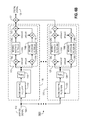
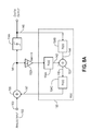
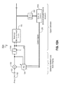
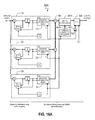
- FIGS. 1A-C illustrate block diagrams of conventional, lowpass oversampling converters.
- a typical conventional oversampling converter uses a delta-sigma ( ⁇ ) modulator 7 A-C to shape or color quantization noise.
- ⁇ delta-sigma
- a delta-sigma modulator 7 A-C shapes the noise that will be introduced by quantizer 10 by performing a difference operation 8 (i.e., delta) and an integration operation 13 A-C (i.e., sigma), e.g.,
- the delta-sigma modulator processes the signal with one transfer function (STF) and the quantization noise with a different transfer function (NTF).
- STF transfer function
- NTF transfer function
- a delta-sigma modulator that employs an auxiliary sample-and-hold operation, either explicitly as in sample-and-hold circuit 6 in converters 5 A&C shown in FIGS. 1A &C, respectively, or implicitly using switched-capacitor circuits (e.g., integrators), for example, is commonly referred to as a discrete-time, delta-sigma (DT ⁇ ) modulator.
- a delta-sigma modulator, such as circuit 7 B shown in FIG. 1B that does not employ an auxiliary sample-and-hold operation is commonly referred to as a continuous-time, delta-sigma (CT ⁇ ) modulator.
- Discrete-time modulators have been the preferred method in conventional converters because DT ⁇ modulators are more reliable in terms of stable (i.e., insensitivity to timing variations) and predictable (i.e., linearity) performance. See Ortmans and Gerfers, “Continuous-Time Sigma-Delta A/D Conversion: Fundamentals, Performance Limits and Robust Implementations”, Springer Berlin Heidelberg 2006.
- An alternative DT ⁇ modulator is the error-feedback structure of converter 5 C shown in FIG. 1C , which has no feed-forward filtering and a single feedback filter.
- the error-feedback structure is conventionally considered suitable for digital implementations (i.e., digital-to-analog conversion), but not for analog implementations due to its increased sensitivity to component mismatches compared to the interpolative structure. See Johns, D. and Martin, K., “Analog Integrated Circuit Design”, John Wiley & Sons 1997.
- conventional oversampling converters employ a comb P+1 or sinc P+1 filter 12 (also referred to in the prior art as a cascaded integrator-comb filter) for output filtering and signal reconstruction.
- Conventional oversampling converters with a first-order noise-shaped response realize the comb P+1 filter 12 in three steps: second-order integration 12 A, e.g., with a transfer function of
- T COMB ( 1 - z - N 1 - z - 1 ) P + 1 , where P is the order of the modulator, produces frequency response minima at multiples of the conversion rate (f CLK ), and conventionally has been considered optimal for oversampling converters.
- P the order of the modulator
- the delta-sigma converters 5 A-C illustrated in FIGS. 1A-C are conventionally known as lowpass, delta-sigma converters.
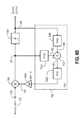
- a variation on the conventional lowpass converter employs bandpass delta-sigma modulators to allow conversion of narrowband signals that are centered at frequencies above zero.
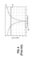
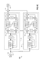
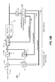
- Exemplary bandpass oversampling converters 40 A&B, illustrated in FIGS. 3A &B, respectively, include a bandpass delta-sigma modulator 42 A or 42 B, respectively, that provides, as shown in FIG. 4 , a signal response 50 and a quantization noise response 51 with a minimum 52 at the center of the converter Nyquist bandwidth (i.e., 1 ⁇ 4 ⁇ f S ).
- Bandpass delta-sigma modulators are similar to the more-common lowpass variety in several respects:
- the conventional bandpass delta-sigma modulator has both discrete-time (converter 40 A shown in FIG. 3A ) and continuous-time (converter 40 B shown in FIG. 3B ) forms.
- the bandpass delta-sigma modulator 42 A&B shapes noise from quantizer 10 by performing a difference operation 8 (i.e., delta) and an integration operation 13 A&B (i.e., sigma), respectively, where
- ⁇ 0 ⁇ ⁇ f s / 2
- the bandpass modulator processes the signal with one transfer function (STF) and the quantization noise with a different transfer function (NTF).
- STF transfer function
- NTF quantization noise with a different transfer function
- NTF ⁇ ( s ) s 2 + ⁇ 2 s 2 + ⁇ ⁇ s + ⁇ 2
- discrete-time modulators have a signal transfer function (STF) that generally is all-pass
- continuous-time modulators have a linearized signal transfer function (STF) that generally is not all-pass (e.g., bandpass for the above example).
- the noise transfer function (NTF) of a real bandpass delta-sigma modulator is at minimum a second-order response.
- oversampling converters can offer very high resolution, but the noise shaping and signal reconstruction process generally limits the utility of oversampling converters to applications requiring only low instantaneous bandwidth.
- multiple oversampling converters can be operated in parallel using the time-interleaving (time-slicing) and/or frequency-interleaving (frequency-slicing) techniques developed originally for Nyquist converters (i.e., flash, pipelined, etc.).
- time-interleaving time-slicing
- frequency-slicing frequency-interleaving
- Each converter in the time-interleaving array is clocked with a different clock phase, such that the conversion operation is distributed in time across multiple converters (i.e., polyphase decomposition). While converter #1 is processing the first sample, converter #2 is processing the next sample, and so on.
- the total bandwidth of the continuous-time signal is uniformly decomposed (i.e., divided) into multiple, narrowband segments (i.e., sub-bands).
- Each parallel processing branch converts one narrowband segment, and all the converter processing branches operate from a single, common sampling clock.
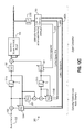
- Conventional frequency-interleaving converters include frequency-translating hybrid (FTH) converters and hybrid filter bank (HFB) converters.
- FTH frequency-translating hybrid
- HFB hybrid filter bank
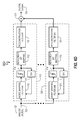
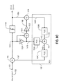
- individual frequency bands are downconverted to baseband and separated out using lowpass filters. More specifically, the input signal 71 is provided to a set of multipliers 72 together with the band's central frequencies 74 A- 76 A.
- the resulting baseband signals are then provided to identical lowpass filters 78 that are designed to spectrally decompose (i.e., slice) the input signal (i.e., a process referred to as signal analysis), in addition to minimizing aliasing.
- Each such filtered baseband signal is then digitized 80 A, digitally upconverted 82 A using digitized sinusoids 83 A-C (or alternatively simply upsampled) and then bandpass filtered 84 A- 86 A in order to restore the input signal to its previous frequency band (i.e., a process referred to as signal synthesis).
- the individual bands are recombined in one or more adders 88 .
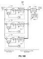
- Each converter 80 A in the interleaved array is able to operate at a lower sampling frequency equal to twice the bandwidth of each subdivided, downcoverted band (i.e., the portion of the input signal intended to be converted by the respective processing branch). Similar processing occurs in HFB converter, except that the individual frequency bands are separated out using analog (frequency decomposition) bandpass filters before downconversion to baseband (see Petraglia, A., “High Speed A/D Conversion using QMF Filter Banks”, Proceedings: IEEE International Symposium on Circuits and Systems, 1990).
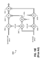
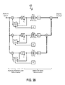
- the conventional parallel delta-sigma analog-to-digital converter ( ⁇ ADC) 70 B shown in FIG. 5B , is similar in design and operation to the conventional frequency-interleaved converter 70 A shown in FIG. 5A , except that oversampling converters 80 B are used in place of multi-bit digitizers 80 A and anti-aliasing filters 78 .
- oversampling converters 80 B are used in place of multi-bit digitizers 80 A and anti-aliasing filters 78 .
- the primary advantage of the prior-art ⁇ converter 70 B is that the oversampling operation of the delta-sigma modulators 89 eliminates the need for the anti-aliasing function provided by the analog frequency decomposition filters.
- the conventional ⁇ ADC generally employs discrete-time, lowpass delta-sigma modulators 89 and uses continuous-time Hadamard sequences (v i (t)) 74 B- 76 B and discrete-time Hadamard sequences (u i [n]) 89 A-C, instead of sinusoidal waveforms, to reduce the circuit complexity associated with the downconversion 72 B and upconversion 82 B operations.
- bandpass delta-sigma modulators are used to eliminate the need for analog downconversion completely, in a process sometimes called Direct Multiband Delta-Sigma Conversion (MB ⁇ ).
- MB ⁇ Direct Multiband Delta-Sigma Conversion
- conventional oversampling frequency-interleaving converters i.e., ⁇ ADC and MB ⁇
- ⁇ ADC and MB ⁇ employ conventional, decimating comb P+1 (sinc P+1 ) lowpass filters ( ⁇ ADC) or a conventional, transversal finite impulse response (FIR) filter bank (MB ⁇ ) for signal reconstruction.
- ⁇ ADC and MB ⁇ employ conventional, decimating comb P+1 (sinc P+1 ) lowpass filters ( ⁇ ADC) or a conventional, transversal finite impulse response (FIR) filter bank (MB ⁇ ) for signal reconstruction.
- FIR finite impulse response
- 6,873,280 addresses conversion of digital (discrete-time, discretely variable) signals to other forms, rather than the conversion of analog (continuous-time, continuously variable) signals to digital signals.
- a third technique described in U.S. Pat. No. 6,683,550, employs multi-bit, first-order modulators which are not suitable for high-precision, bandpass oversampling applications since these application require modulators that are at least second order.
- the present invention provides an improved ADC, particularly for use at very high sample rates and instantaneous bandwidths approaching the Nyquist limit.
- one specific embodiment of the invention is directed to an apparatus for converting a continuous-time, continuously variable signal into a sampled and quantized signal.
- the apparatus includes: an input line for accepting an input signal that is continuous in time and continuously variable; a plurality of processing branches coupled to the input line; and an adder coupled to outputs of the plurality of processing branches, with each of the processing branches including: (a) a continuous-time filter, preferably a Diplexing Feedback Loop (DFL), for shaping quantization and other noise, (b) a sampling/quantization circuit coupled to the output of the quantization-noise-shaping continuous-time filter, (c) a digital bandpass filter, preferably a Bandpass Moving Average filter, coupled to an output of the sampling/quantization circuit, and (d) one or more lines coupling the input and output of the sampling/quantization circuit back into the quantization-noise-shaping continuous-time filter.
- DFL Diplexing Feedback Loop
- Each of the quantization-noise-shaping continuous-time filters has an adder that includes multiple inputs and an output, with: 1) the input signal being coupled to one of the inputs of the adder, 2) the output of the adder being coupled to a sampling/quantization circuit input and to one of the inputs of the adder through a first filter, and 3) the output of the sampling/quantization circuit in the same processing branch being coupled to one of the inputs of the adder through a second filter.
- the response of each of the first filter and the second filter preferably includes a lowpass component, and preferably, the second filter has a different transfer function than the first filter.
- the quantization-noise-shaping continuous-time filters in different ones of the processing branches produce quantization noise minima at different frequencies, and the quantization noise minimum for each of the quantization-noise-shaping continuous-time filters corresponds to a frequency band selected by the digital bandpass filter in the same processing branch.
- the apparatus includes: an input line for accepting an input signal that is continuous in time and continuously variable, multiple processing branches coupled to the input line, and an adder coupled to outputs of the processing branches.
- Each of the processing branches includes: (a) a continuous-time quantization-noise-shaping circuit, (b) a sampling/quantization circuit coupled to an output of the continuous-time quantization-noise-shaping circuit, (c) a digital bandpass filter coupled to an output of the sampling/quantization circuit, and (d) a line coupling the output of the sampling/quantization circuit back into the continuous-time quantization-noise-shaping circuit.
- a center frequency of the digital bandpass filter in each processing branch corresponds to a minimum in a quantization noise transfer function for the continuous-time quantization-noise-shaping circuit in the same processing branch.
- Each of the digital bandpass filters includes: (a) a quadrature frequency downconverter that has in-phase and quadrature outputs, (b) a first moving-average filter coupled to the in-phase output of the quadrature frequency downconverter, (c) a second moving-average filter coupled to the quadrature output of the quadrature frequency downconverter, and (d) a quadrature frequency upconverter coupled to outputs of the first and second moving-average filters.
- the invention is directed to an apparatus for converting a continuous-time, continuously variable signal into a sampled and quantized signal, and includes: an input line for accepting an input signal that is continuous in time and continuously variable; a plurality of processing branches coupled to the input line; and a combining circuit, coupled to outputs of a plurality of the processing branches, that combines signals on such outputs into a final output signal.
- Each of such processing branches includes: (a) a bandpass quantization-noise-shaping circuit, (b) a sampling/quantization circuit coupled to an output of the bandpass noise-shaping circuit, (c) a digital bandpass filter coupled to an output of the sampling/quantization circuit, and (d) a line coupling the output of the sampling/quantization circuit back into the bandpass noise-shaping circuit.
- a center frequency of the digital bandpass filter in each processing branch corresponds to a minimum or a stopband region in a quantization noise transfer function for the bandpass noise-shaping circuit in the same processing branch.
- Each of the digital bandpass filters includes: (a) a quadrature frequency downconverter that has in-phase and quadrature outputs, (b) a first lowpass filter coupled to the in-phase output of the quadrature frequency downconverter, (c) a second lowpass filter coupled to the quadrature output of the quadrature frequency downconverter, and (d) a quadrature frequency upconverter coupled to outputs of the first and second lowpass filters.
- At least one of, a plurality of, or each of the lowpass filters preferably: (i) is implemented as a moving-average filter and/or (ii) has a frequency response which varies approximately in magnitude versus frequency according to the product of raised sin(x)/x functions.
- a further embodiment is directed to an apparatus for converting a continuous-time, continuously variable signal into a sampled and quantized signal.
- the apparatus includes: an input line for accepting an input signal that is continuous in time and continuously variable, multiple processing branches coupled to the input line, and an adder coupled to outputs of the plurality of processing branches
- Each of the processing branches includes: (a) a bandpass quantization-noise-shaping circuit, (b) a multi-bit sampling/quantization circuit coupled to an output of the bandpass quantization-noise-shaping circuit, (c) a nonlinear bit-mapping circuit coupled to an output of the multi-bit sampling/quantization circuit, (d) a digital bandpass filter coupled to an output of the nonlinear bit-mapping circuit, (e) a digital-to-analog converter (DAC) circuit coupled to the output of the multi-bit sampling/quantization circuit, and (f) a line coupling an output of the digital-to-analog converter circuit back into the bandpass quantization-
- a center frequency of the digital bandpass filter in each processing branch corresponds to a minimum in a quantization noise transfer function for the continuous-time quantization-noise-shaping circuit in the same processing branch.
- the nonlinear bit-mapping circuit in each of the processing branches performs a scaling operation, on a bit-by-bit basis, that matches imperfections in a binary scaling response of the digital-to-analog converter in the same processing branch.
- the apparatus preferably includes: (a) a first input line for accepting a high-resolution (or at least relatively high-resolution) version of an input signal, (b) a second input line for accepting a low-resolution (or at least a relatively lower-resolution, e.g., coarsely-quantized) version of the input signal, (c) a quantization noise estimator, which is coupled to the first and second input lines, and which preferably generates a high-resolution error signal that in a particular frequency band, is proportional to the difference between the high-resolution input signal and the coarsely-quantized version of the input signal; (d) a quantization element that is coupled to the output of the quantization noise estimator and converts the high-resolution error signal into a preferably coarsely-quantized error signal; (e) a downconverter (e.g., downsampler) which is coupled to the
- the original frequency band of the error signal typically is centered at a frequency which is equal to, or is at least approximately equal to, a frequency coinciding with an intended spectral minimum in the noise transfer function of the bandpass quantization-noise-shaping circuit.
- the adaptive control component preferably minimizes the level detector output by adjusting a parameter within the bandpass quantization-noise-shaping circuit.
- the invention also encompasses an apparatus for converting a continuous-time, continuously variable signal into a sampled and quantized signal at a final sampling rate.
- the apparatus includes: an input line for accepting an input signal that is continuous in time and continuously variable, multiple sampling/quantization circuits coupled to the input line, and an adder coupled to outputs of the plurality of sampling/quantization circuits.
- Each of the sampling/quantization circuits operates at a subsampled rate (i.e., sub-rate), which is less than the final sampling rate (i.e., a full-rate).
- each sampling/quantization circuit subsamples on a different phase of a sub-rate clock, such that the subsampling instants associated with each of the sampling/quantization circuits are offset in time by increments which are integer multiples of the full-rate sampling period.
- the adder combines (i.e., sums) the subsampled outputs of each of the sampling/quantization circuits, to produce an output which represents a filtered version of the input signal, where, preferably: 1) the filter response applied to the input signal includes a lowpass function having a bandwidth smaller than one-half the maximum sampling rate; 2) the filter response applied to the input signal is equivalent to that of a zero-order hold at the subsampled rate; and/or 3) the magnitude of the filter response applied to the input signal decreases with angular frequency ⁇ according to a sin ( ⁇ )/ ⁇ function.
- Such apparatuses typically can provide a better combination of high resolution and wide bandwidth than is possible with conventional converters and can be used for various commercial, industrial and military applications, e.g., in various direct conversion sensors, software-defined or cognitive radios, multi-channel communication receivers, all-digital RADAR systems, high-speed industrial data acquisition systems, ultra-wideband (UWB) communication systems.
- various direct conversion sensors e.g., software-defined or cognitive radios, multi-channel communication receivers, all-digital RADAR systems, high-speed industrial data acquisition systems, ultra-wideband (UWB) communication systems.
- UWB ultra-wideband
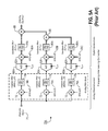
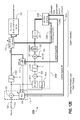
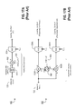
- FIG. 1A is a block diagram of a conventional lowpass oversampling converter having a discrete-time, interpolative delta-sigma modulator with first-order response
- FIG. 1B is a block diagram of a conventional lowpass oversampling converter having a continuous-time, interpolative delta-sigma modulator with first-order response
- FIG. 1C is a block diagram of a conventional oversampling lowpass converter having a discrete-time, error-feedback delta-sigma modulator with first-order response.
- FIG. 2 illustrates the input signal transfer function (STF) and quantization-noise transfer function (NTF) for a conventional, first-order, lowpass delta-sigma modulator.
- STF input signal transfer function
- NTF quantization-noise transfer function
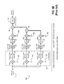
- FIG. 3A is a block diagram of a single-band bandpass oversampling converter having a discrete-time, interpolative delta-sigma modulator with second-order response
- FIG. 3B is a block diagram of a single-band bandpass oversampling converter having a continuous-time, interpolative delta-sigma modulator with second-order response.
- FIG. 4 illustrates the input signal transfer function (STF) and quantization-noise transfer function (NTF) for the delta-sigma modulator of the single-band bandpass converters shown in FIGS. 3A &B.
- STF input signal transfer function
- NTF quantization-noise transfer function
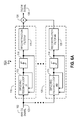
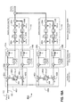
- FIG. 5A is a block diagram of a conventional frequency-interleaving converter
- FIG. 5B is a block diagram of a conventional parallel delta-sigma modulator converter ( ⁇ ADC).
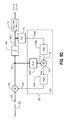
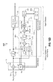
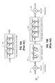
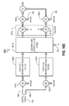
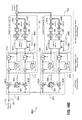
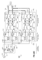
- FIG. 6A is a simplified block diagram of a Multi-Channel Bandpass Oversampling (MBO) converter according to one representative embodiment of the present invention that employs a Diplexing Feedback Loop for noise shaping
- FIG. 6B is a simplified block diagram of a Multi-Channel Bandpass Oversampling (MBO) converter according to a second representative embodiment of the present invention that employs a Bandpass Moving-Average filter for signal reconstruction
- FIG. 6C is a simplified block diagram of a Multi-Channel Bandpass Oversampling (MBO) converter according to a third representative embodiment of the present invention that employs a Diplexing Feedback Loop for noise shaping and a Bandpass Moving-Average filter for signal reconstruction
- 6D is a simplified block diagram of a Multi-Channel Bandpass Oversampling (MBO) converter according to a fourth representative embodiment of the present invention that employs a multi-bit sampling/quantization circuit and feedback digital-to-analog converter (DAC) in conjunction with a nonlinear bit mapping function.
- MBO Multi-Channel Bandpass Oversampling
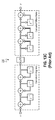
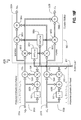
- FIG. 7 is a more detailed block diagram of an exemplary MBO processing branch according to a representative embodiment of the present invention.
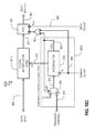
- FIG. 8A is a block diagram illustrating a Diplexing Feedback Loop (DFL) according to a representative embodiment of the present invention that employs single-bit quantization and a feedback diplexer to produce quantization noise response minima at arbitrary frequencies, with signal amplification occurring at the input of the feedback diplexer;
- FIG. 8B is a block diagram illustrating a Diplexing Feedback Loop (DFL) according to a representative embodiment of the present invention that employs single-bit quantization and a feedback diplexer to produce quantization noise response minima at arbitrary frequencies, with signal amplification occurring at the output of the feedback diplexer;
- DFL Diplexing Feedback Loop
- FIG. 8C is a block diagram illustrating a Diplexing Feedback Loop (DFL) according to a representative embodiment of the present invention that employs single-bit quantization, active feedback gain with distortion mitigation, and a feedback diplexer to produce quantization noise response minima at arbitrary frequencies;
- FIG. 8D is a block diagram illustrating a Diplexing Feedback Loop (DFL) according to a representative embodiment of the present invention that employs multi-bit quantization, with nonlinear bit mapping, and a feedback diplexer to produce quantization noise response minima at arbitrary frequencies;
- FIG. 8E is a block diagram illustrating a nonlinear bit-mapping function according to a representative embodiment of the present invention that uses digital multipliers and digital adders to produce nonlinear distortion;
- FIG. 8F is a block diagram illustrating a linearized model of a Diplexing Feedback Loop (DFL) according to a representative embodiment of the present invention that incorporates errors due to quantization, nonlinear bit mapping, and a feedback digital-to-analog (D/A) conversion
- FIG. 8G is a block diagram illustrating a Diplexing Feedback Loop (DFL) according to a representative embodiment of the present invention that employs multiple sampling/quantization circuits which introduce a zero-order hold response at a subsampled rate.
- DFL Diplexing Feedback Loop
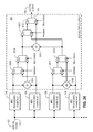
- FIGS. 9A &B are circuit diagrams illustrating exemplary implementations of Diplexing Feedback Loop (DFL) noise shaping for negative trimming/calibration of f notch values using reactive networks for signal summing and signal distribution
- FIGS. 9C &G are circuit diagrams illustrating exemplary implementations of Diplexing Feedback Loop (DFL) noise shaping for positive trimming/calibration of f notch values using multi-bit quantization and reactive networks for signal summing and signal distribution
- FIG. 9D is a circuit diagram illustrating an exemplary implementation of Diplexing Feedback Loop (DFL) noise shaping for negative trimming/calibration of f notch values using resistive networks for signal summing and signal distribution
- FIGS. 9E &F are circuit diagrams illustrating exemplary implementations of Diplexing Feedback Loop (DFL) noise shaping for positive trimming/calibration of f notch values using resistive networks for signal summing and signal distribution.
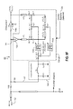
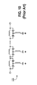
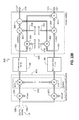
- FIG. 10 illustrates a circuit diagram of a conventional, lumped-element delay network for use in a representative embodiment of the present invention.
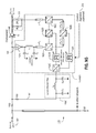
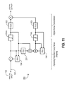
- FIG. 11 is a block diagram of an exemplary fourth-order Diplexing Feedback Loop (DFL) noise shaping circuit using a parallel circuit arrangement.
- DFL Diplexing Feedback Loop
- FIG. 12A illustrates a second-order Diplexing Feedback Loop (DFL) noise shaping circuit that employs single-bit quantization and uses active calibration, based on Bandpass Moving-Average filter output levels, to dynamically adjust the diplexer filter responses
- FIG. 12B illustrates a second-order Diplexing Feedback Loop (DFL) noise shaping circuit that employs multi-bit quantization and uses active calibration, based on Bandpass Moving-Average filter output levels, to dynamically adjust 1) diplexer filter responses, 2) nonlinear bit-mapping distortion, and 3) feedback digital-to-analog converter (DAC) transfer function
- DFL Diplexing Feedback Loop
- FIG. 12C illustrates a fourth-order Diplexing Feedback Loop (DFL) noise shaping circuit that employs single-bit quantizers and uses active calibration, based on Bandpass Moving-Average filter output levels, to dynamically adjust 1) diplexer filter responses and 2) error cancellation (digital) filter response;
- FIG. 12D illustrates a second-order Diplexing Feedback Loop (DFL) noise shaping circuit that employs single-bit quantization and uses active calibration, based on average quantization error levels, to dynamically adjust the diplexer filter responses; and FIG.
- DFL Diplexing Feedback Loop
- DFL Diplexing Feedback Loop
- FIG. 13A is a block diagram illustrating a conventional structure for implementing a bandpass, signal-reconstruction filtering using a digital (e.g., Hann) bandpass finite-impulse-response (FIR) filter
- FIG. 13B is a block diagram illustrating a conventional structure for bandpass, signal-reconstruction filtering using: (a) digital demodulation, (b) comb P+1 decimation, (c) complex digital (e.g., Hann) lowpass FIR filtering, and (d) remodulation
- FIG. 13C is a block diagram illustrating a conventional structure for lowpass, signal reconstruction using a comb 3 (i.e., sinc 3 ) digital filter comprised of cascaded integrators and differentiators, with decimation by N.
- a comb 3 i.e., sinc 3
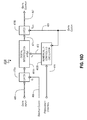
- FIG. 14A is a block diagram of a Bandpass Moving Average (BMA) signal-reconstruction filter according to a representative embodiment of the invention that includes a single, complex tap equalizer and recursive moving-average filters with quadrature frequency conversion
- FIG. 14B is a block diagram of a Bandpass Moving Average (BMA) signal reconstruction filter according to a representative embodiment of the invention that includes a single, real tap equalizer and recursive moving-average filters with quadrature frequency conversion
- FIGS. 14C-E are block diagrams illustrating representative forms of recursive moving-average prototype filters for BMA signal reconstruction
- FIG. 15A illustrates frequency responses of a Bandpass Moving Average signal reconstruction filter bank used in a MBO converter according to a representative embodiment of the present invention
- FIG. 15B illustrates the frequency responses of a conventional signal reconstruction FIR filter bank based on a Kaiser window function.
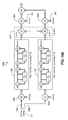
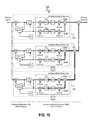
- FIGS. 16A &B are block diagrams of complete MBO converters according to representative embodiments of the present invention, which incorporate: 1) multiple Diplexing Feedback Loops (DFLs) for quantization noise shaping, 2) a Bandpass Moving Average (BMA) filter bank for signal reconstruction, and 3) multiple polynomial interpolators for digital resampling;
- FIG. 16C is a block diagram illustrating an exemplary implementation of a digital resampling circuit that compensates for the difference between a higher sample rate and a lower conversion rate, where the ratio of the sample rate to conversion rate is a rational number;
- FIG. 16D is a block diagram illustrating an exemplary implementation of a digital resampling circuit that compensates for the difference between a sample rate and a conversion rate, where the ratio of the sample rate to conversion rate is an irrational number
- FIG. 16E is a block diagram of a Bandpass Moving Average (BMA) signal-reconstruction filter according to a representative embodiment of the invention that includes a quadrature interpolator, in addition to a single, complex tap equalizer and recursive moving-average filters with quadrature frequency conversion; and FIG.
- BMA Bandpass Moving Average
- 16F is a block diagram of a polynomial estimator (interpolator) according to a representative embodiment of the invention that operates on complex-valued signals (i.e., signals with in-phase/real and quadrature/imaginary components) and fabricates new data samples from existing data samples according to a linear (i.e., first-order) function.
- interpolator a polynomial estimator
- FIG. 17A is a block diagram of a conventional ADC that employs a simple downconverter to extend the frequency range of the ADC; and FIG. 17B is a block diagram of a conventional ADC that uses quadrature downconversion and multiple converters to extend the frequency range of the ADC(s).
- FIG. 18A is a block diagram of a complete MBO converter according to a representative embodiment of the present invention, which incorporates multiple Diplexing Feedback Loops (DFLs) with dedicated quadrature downconversion to zero hertz at each DFL input;
- FIG. 18B is a block diagram of a complete MBO converter according to a representative embodiment of the present invention, which incorporates multiple Diplexing Feedback Loops (DFLs) and dedicated quadrature downconversion to a non-zero, intermediate frequency at each DFL input;
- DFLs Diplexing Feedback Loops
- FIG. 18C is a block diagram of a complete MBO converter according to a representative embodiment of the present invention, which incorporates multiple Diplexing Feedback Loops (DFLs) and shared quadrature downconversion to a non-zero, intermediate frequency at each DFL input;
- FIG. 18D is a block diagram of a Bandpass Moving Average (BMA) signal-reconstruction filter according to a representative embodiment of the invention that incorporates: 1) complex frequency downconversion with compensation for quadrature imbalance, 2) recursive moving-average filtering, 3) gain/phase (single, complex tap) equalization, and 4) quadrature frequency upconversion with preferred compensation for quadrature imbalance;
- FIG. 18E is a block diagram of a quadrature frequency upconverter that incorporates conventional compensation for quadrature imbalance.
- BMA Bandpass Moving Average
- FIG. 19 is a block diagram of a complete MBO converter according to a representative embodiment of the present invention, which incorporates multiple Diplexing Feedback Loop (DFL) noise shaping circuits in conjunction with a Bandpass Moving Average (BMA) filter bank for signal reconstruction.
- DFL Diplexing Feedback Loop
- BMA Bandpass Moving Average
- FIG. 20 is a block diagram of a complete MBO converter according to a first alternate representative embodiment of the present invention, which incorporates multiple Diplexing Feedback Loop (DFL) noise shaping circuits in conjunction with a conventional FIR filter bank for signal reconstruction.
- DFL Diplexing Feedback Loop
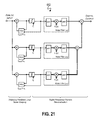
- FIG. 21 is a block diagram of a complete MBO converter according to a second alternate embodiment of the present invention, which incorporates multiple Diplexing Feedback Loop (DFL) noise shaping circuits in conjunction with a frequency-domain filter bank for signal reconstruction.
- DFL Diplexing Feedback Loop
- FIG. 22A is a block diagram of a complete MBO converter according to a representative embodiment of the present invention, which incorporates multiple Diplexing Feedback Loops (DFLs) and includes Bandpass Moving Average (BMA) filters that generate a complex output as quadrature components
- FIG. 22B is a block diagram of a Bandpass Moving Average (BMA) signal-reconstruction filter according to a representative embodiment of the invention that incorporates: 1) quadrature frequency downconversion, 2) gain/phase (single, complex tap) equalization, 3) recursive moving-average filtering, and 4) quadrature frequency upconversion which generates separate in-phase and quadrature outputs;
- FIG. 22A is a block diagram of a complete MBO converter according to a representative embodiment of the present invention, which incorporates multiple Diplexing Feedback Loops (DFLs) and includes Bandpass Moving Average (BMA) filters that generate a complex output as quadrature components
- FIG. 22B is a block diagram of a Bandpass Moving Average (BMA) signal-
- FIG. 22C is a block diagram of a complete MBO converter according to a representative embodiment of the present invention, which incorporates: 1) multiple Diplexing Feedback Loops (DFLs), 2) shared quadrature downconversion to a non-zero, intermediate frequency at each DFL input, and 3) Bandpass Moving Average (BMA) filters that generate a complex output as quadrature components; and
- FIG. 22D is a block diagram of a Bandpass Moving Average (BMA) signal-reconstruction filter according to a representative embodiment of the invention that incorporates: 1) quadrature frequency downconversion which accepts separate in-phase and quadrature inputs, 2) recursive moving-average filtering, and 4) quadrature frequency upconversion which generates separate in-phase and quadrature outputs.
- DFLs Diplexing Feedback Loops
- BMA Bandpass Moving Average
- FIG. 23 is a block diagram of a complete MBO converter illustrating an exemplary method for signal distribution across multiple converter processing branches.
- FIG. 24 is a block diagram of a Multi-Mode MBO converter that employs an output Add-Multiplex Array (AMA) network to enable: (a) isolation of individual MBO processing branches for operation as multiple narrowband output channels, or (b) combination of individual MBO processing branches for operation as fewer wideband output channels.
- AMA Add-Multiplex Array
- a preferred converter according to the present invention uses a technique that sometimes is referred to herein as Multi-Channel Bandpass Oversampling (MBO).
- MBO Multi-Channel Bandpass Oversampling
- ⁇ parallel delta-sigma
- MB ⁇ multiband delta-sigma
- a MBO converter incorporates one or more of the following technological innovations to improve instantaneous bandwidth and resolution: 1) continuous-time, Diplexing Feedback Loops (DFLs) are used in place of delta-sigma ( ⁇ ) modulators, e.g., to improve quantization noise shaping at very high converter sample rates; 2) bandpass (preferably second-order or higher) oversampling eliminates the need for analog downconversion using sinusoidal waveforms or Hadamard sequences (e.g., as in ⁇ converters); 3) Bandpass Moving-Average (BMA) filter banks are used in place of decimating comb P+1 filters (i.e., ⁇ ), conventional FIR filter banks (i.e., MB ⁇ ), or Hann window function FIR filters to minimize phase and amplitude distortion and significantly reduce signal-processing complexity; 4) a nonlinear bit-mapping function is applied to the output of the sampling/quantization circuit so that errors made in converting the digital output of the sampling/quantization circuit to
- Such techniques can in some respects be thought of as a unique and novel method of combining two distinct conventional techniques—continuous-time, bandpass oversampling and multi-channel, frequency-interleaving. As discussed in more detail below, the use of such techniques often can overcome the problems of limited conversion resolution and precision at very high instantaneous bandwidths.
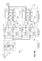
- converters 100 A-D separately processes M different frequency bands for a continuous-time continuously variable signal 102 , using a separate branch (e.g., branch 110 or 120 ) to process each such band, and then sum up all the branch outputs in an adder 131 in order to provide the output digital signal 135 .
- the M different frequency bands are orthogonal, or at least approximately orthogonal, with respect to the converter output data rate.
- the signal 102 is input on a line 103 that could be implemented, e.g., as a physical port for accepting an external signal or as an internal wire, conductive trace or a similar conductive path for receiving a signal from another circuit within the same device.
- the input signal 102 is provided directly to each of the branches (e.g., branches 110 and 120 ).
- the input line 103 can be coupled to such branches in any other manner.
- the term “coupled”, or any other form of the word is intended to mean either directly connected or connected through one or more other processing blocks, e.g., for the purpose of preprocessing.
- any number of branches may be used and, as discussed in more detail below, increasing the number of branches generally increases the resolution of the converters 100 A-D.
- each such branch primarily processes a different frequency band and includes: 1) a Diplexing Feedback Loop (e.g., DFL 113 or 123 of converters 100 A&C) or other quantization-noise-shaping circuit (e.g., circuit 113 or 123 of converter 100 B, either or both potentially being a conventional discrete-time or continuous-time quantization-noise-shaping circuit); 2) a sampling/quantization circuit 114 ; and 3) a Bandpass Moving-Average (BMA) reconstruction filter (e.g., BMA filter 115 or 125 of converters 100 B&C) or other bandpass reconstruction filter (e.g., filter 115 or 125 of converter 100 A).
- BMA Bandpass Moving-Average
- Each quantization-noise-shaping circuit (e.g., circuit 113 or 123 ) realizes a quantization noise response (NTF) with a minimum (i.e., notch or null) at or near the frequency band(s) (more preferably, the center of the frequency band(s)) that is/are intended to be processed by its respective branch.
- NTF quantization noise response
- Each sampling/quantization circuit 114 preferably is identical to the others and is implemented as a single-bit quantizer, sometimes referred to herein as a hard limiter, or a multi-bit quantizer.
- each branch preferably incorporates a nonlinear bit-mapping function (e.g., circuit 112 of converter 100 D), so that the digital input to the reconstruction filter (e.g., conventional filter 115 or 125 of converter 100 D) accurately represents the analog signal that is fed back into the continuous-time quantization-noise-shaping circuit (e.g., conventional circuit 113 or 123 of converter 100 D).
- a nonlinear bit-mapping function e.g., circuit 112 of converter 100 D
- the signal input into sampling/quantization circuit 114 and the signal output by sampling/quantization circuit 114 preferably are fed back, diplexed (i.e., independently filtered, combined, and then optionally jointly filtered), and combined with the input signal 102 so that quantization errors in earlier samples can be taken into account in generating later quantized samples (i.e., noise shaping using a Diplexing Feedback Loop).
- quantization errors and noise are shaped using a conventional means, such as discrete-time or continuous-time ⁇ modulation.
- Each digital bandpass filter preferably a Bandpass Moving-Average filter according to the representative embodiments of converters 100 B&C (e.g., filter 115 or 125 ), selects out the frequency band being processed within its respective branch. As shown in FIGS.
- each such filter preferably includes a quadrature frequency downconverter (e.g., using multipliers 118 A&B or 128 A&B) having in-phase and quadrature outputs, a moving-average filter (e.g., 116 A or 126 A) coupled to the in-phase output of the quadrature frequency downconverter, a moving-average filter (e.g., 116 B or 126 B) coupled to the quadrature output of the quadrature frequency downconverter, and a quadrature frequency upconverter (e.g., using multipliers 118 C&D or 128 C&D) coupled to outputs of such moving-average filters, with the downconverter and upconverter using cosine and sine sequences, respectively, having a frequency corresponding to the minimum in the quantization noise transfer function.
- a quadrature frequency downconverter e.g., using multipliers 118 A&B or 128 A&B
- a moving-average filter e.g., 116
- the frequency band being processed within a respective branch is selected out using a conventional filter, such as a transversal FIR filter.
- the adder 131 which can be implemented, e.g., as a single adder with multiple inputs or as a series of two-input adders, combines the outputs of the digital bandpass filters.
- a hard limiter for the sampling/quantization circuits 114 generally is preferred.
- use of a hard limiter has the advantage that the two-level (digital) output of the hard limiter can be converted to an analog feedback signal (i.e., digital-to-analog conversion) without introducing the differential nonlinearities or rounding errors (as opposed to quantization noise) associated with the digital-to-analog (D/A) conversion of multi-bit quantizer outputs.
- nonlinear compensation preferably is realized by applying a nonlinear bit-mapping function 112 to the output of sampling/quantization circuit 114 .
- Nonlinear bit-mapping function 112 replicates the nonlinearities at the output of digital-to-analog converter (DAC) 111 , such that the input to the reconstruction filter (e.g., filter 115 and 125 ) is a more precise digital representation of the actual analog signal that is fed back into continuous-time quantization-noise-shaping filter (e.g., filter 113 or 123 ).
- a more precise digital representation of the analog feedback signal ensures that quantization errors in earlier samples are accurately taken into account in generating later quantized samples to effectively subject feedback DAC nonlinearities to the noise-shaped response of the quantization-noise-shaping filter.
- a desired overall effective resolution of the converters 100 A-D generally can be achieved, independent of the sample rate (f S ), by appropriately selecting design parameters such as the number of processing branches M (corresponding to the number of individual frequency bands processed) and the quality of the filters used (e.g., the order of the noise-shaped response and the stopband attenuation of the bandpass reconstruction filter).
- each of the circuits used for shaping quantization noise is a DFL because such a circuit has been found to achieve the best combination of effectiveness, ease of construction and ease of configuration (i.e., converters 100 A&C of FIGS. 6A &C).
- converters 100 A&C of FIGS. 6A &C converters 100 A&C of FIGS. 6A &C.
- ⁇ continuous-time delta-sigma
- the primary considerations for the quantization-noise-shaping circuits to be used preferably derive from the desire for stable and accurate operation at very high sample rates.
- each quantization-noise-shaping circuit has at least the following three properties: 1) the primary performance impairments of the quantization-noise-shaping circuit, such as those related to settling-time errors, sampling uncertainty/jitter, thermal noise, and quantization/rounding errors, are subject to a noise-shaped response and/or bandlimiting; 2) the performance of the quantization-noise-shaping circuit is relatively insensitive to non-ideal circuit behavior and excess feedback loop delay; and 3) the quantization-noise-shaping circuit can be implemented using high-frequency design techniques, such as those utilizing distributed-element circuits and monolithic microwave integrated circuits (MMICs). Achieving these properties generally precludes the use of conventional delta-sigma modulators for the noise shaping operation of the preferred embodiments.
- MMICs monolithic microwave integrated circuits
- the conventional DT ⁇ modulator generally is not preferable for use in the MBO converter because the auxiliary (explicit or implicit) sample-and-hold operation of the DT ⁇ modulator introduces impairments, such as settling-time errors, output droop, and nonlinear distortion, that are not subject to a noise-shaped response and, therefore, limit the performance of the DT ⁇ modulator at high frequencies.
- the operating frequency of the DT ⁇ modulator is limited by the sampling speed of the auxiliary, high-precision sample-and-hold operation.
- the conventional CT ⁇ modulator is not preferable for use in the MBO converter because, although the impairments of the single, coarse sampling/quantization operation can be subjected to a noise-shaped response, the feed-forward filtering (i.e., for noise integration) of the conventional CT ⁇ modulator generally requires (1) high-linearity, transconductance stages (i.e., current sources); (2) high-gain operational amplifiers (i.e., voltage sources); (3) high-quality (Q), lumped-element parallel resonators (i.e., discrete inductors and capacitors); and/or (4) feedback digital-to-analog converters (DACs) that use twice rate clocks to produce return-to-zero (RZ) and half-delayed return-to-zero (HRZ) outputs.
- DACs digital-to-analog converters
- CT ⁇ modulator can operate at higher frequencies than the DT ⁇ modulator, due to the absence of an auxiliary sample-and-hold function, the performance of CT ⁇ modulator implementations is limited by imperfect integration related to the non-ideal behavior of the active and reactive lumped circuit elements that comprise the continuous-time filter in the modulator feed-forward path, particularly when operating at very high sample rates.
- lumped-element devices instead behave like distributed-element devices: 1) the output impedance degradation of transconductance stages and limited gain of operational amplifiers cause them to behave less like current or voltage sources and more like basic amplifiers (i.e., power output versus current or voltage output); and 2) the parasitic impedances of reactive components, like inductors and capacitors, cause them to behave like low-Q series or parallel resonators. Still further, the non-ideal behavior of lumped circuit elements degrades the linearity and bandwidth of the feed-forward filter and thereby limits the operating frequency of the CT ⁇ modulator.
- CT ⁇ modulator problems with the CT ⁇ modulator are that: (i) the settling errors and sampling jitter of the clocked feedback digital-to-analog converter (DAC) are not subjected to a noise-shaped response or otherwise mitigated, and (ii) the feedback (excess) loop delay introduced by the finite settling time of the feedback DAC degrades the stability and quality of the noise-shaped response by increasing the order of an interpolative modulator.
- DAC clocked feedback digital-to-analog converter
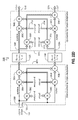
- the present inventor has discovered a new technique for shaping quantization and other noise, referred to herein as a Diplexing Feedback Loop (DFL), that, compared to conventional delta-sigma modulators, incorporates several significant technological innovations to improve operating frequency and performance stability.
- DFL operates as a continuous-time circuit (i.e., processing continues-time continuously variable signals), as opposed to a discrete-time circuit.
- auxiliary sample-and-hold function explicit or implicit
- clocked feedback DAC function that limits speed and accuracy.
- the discrete-time input of the DFL's feedback DAC is transparently converted to a continuous-time output, eliminating the jitter errors associated with clocked (i.e., edge-triggered) DAC devices.
- the DFL can be configured to produce bandpass (e.g., second order or higher) noise-shaped responses or lowpass noise-shaped responses.
- bandpass e.g., second order or higher
- the DFL noise shaper has utility in converter applications where the input signal is not centered at zero frequency.
- the DFL employs passive feedback filter (diplexer) structures to realize perfect integrators that produce quantization noise notches at pre-selected frequencies, but are relatively insensitive to excess feedback loop delay because feedback delay is fundamental to the integration operation.
- passive filters are capable of high-frequency operation because they can be implemented using distributed-element and microwave design techniques.
- the DFL can employ tunable feedback elements for dynamic calibration of the quantization noise transfer function (NTF).
- NTF quantization noise transfer function
- the architecture of the DFL is such that the nonlinear distortion of the digital-to-analog conversion operation in the feedback path (feedback DAC) can be mitigated by using active calibration or by predistorting the quantizer output e.g., using nonlinear bit-mapping). Therefore, impairments introduced by feedback DAC can be significantly attenuated during the signal reconstruction process. For these reasons, among others, the preferred embodiment of the MBO converter uses the DFL approach for shaping quantization and other noise.
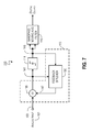
- FIG. 7 A simplified block diagram of a MBO processing branch having a Diplexing Feedback Loop 113 that utilizes a feedback diplexer 150 is shown in FIG. 7 .
- the feedback diplexer 150 inputs the signal 141 that is input into sampling/quantizing circuit 114 , inputs the signal 146 that is output from sampling/quantizing circuit 114 , and outputs a correction signal 147 that is additively combined (in adder 155 ) with the signal on input line 103 .
- signal 147 is produced by separately filtering signals 141 and 146 and then additively combining the filtered signals.
- FIGS. 8A &B Simplified block diagrams of exemplary DFLs, employing a feedback diplexer 150 in combination with a single-bit sampling/quantization circuit 114 A, are shown in FIGS. 8A &B; and a simplified block diagram of an exemplary DFL, employing a feedback diplexer 150 , in combination with a multi-bit sampling/quantization circuit 114 B, a nonlinear bit-mapping operation 112 , and digital-to-analog converter 111 , is shown in FIG. 8D .
- the improved circuit described in the '668 Application is preferred.
- any other multi-bit sampling/quantization circuit such as the conventional circuit described in the '668 Application.
- the shaping of quantization noise is continuous-time and does not employ any filtering in the modulator feed-forward path (between adder 155 and sampler/quantization circuit 114 A or 114 B).
- a signal 141 (that is output from adder 155 and input into sampler/quantizer 114 A) is amplified using feedback amplifier 152 A with gain G, and independently filtered 154 A, using a filter transfer function H 1 (s), thereby resulting in signal 142 .
- the feedback gain can be integrated into diplexer response 154 A without loss of generality, or as illustrated in FIG. 8B , can be moved to the output of feedback diplexer 150 (i.e., or equivalently, integrated into diplexer response 154 C).
- filters 154 A-C include just basic amplifiers, attenuators, distributed delay elements, and reactive components. Depending upon the filter parameters, filters 154 A&B can be all-pass or can have appreciable magnitude variation across the relevant bandwidth that is being processed in the corresponding processing branch.
- Imperfections in amplifier 152 A cause its gain to vary as a function of its input signal amplitude (i.e., the gain is not constant). More specifically, limited supply-voltage headroom causes the large-signal gain of amplifier 152 A to be lower than the small-signal gain of amplifier 152 A (i.e., gain decreases as the input signal level increases).
- This varying gain phenomenon referred to in the prior art as gain compression or AM-AM conversion, introduces nonlinear distortion that is not subjected to the noise-shaped response of the DFL, and therefore, increases the quantization noise at the output of the bandpass reconstruction filters (e.g., filters 115 and 125 in FIGS. 6A &B).
- the present inventor has discovered means for mitigating the nonlinear distortion of amplifier 152 A.
- One such mitigation means illustrated in FIG. 8C , uses subtractor 151 A and amplifier 152 B to create a replica (i.e., signal 148 ) of the nonlinear distortion introduced by amplifier 152 A.
- the replicated nonlinear distortion is summed with the output of quantizer 114 B, using adder 151 B, and eventually is cancelled in subtractor 153 (i.e., after filtering by diplexer response 154 B).
- amplifier 152 B introduces significantly less nonlinear distortion compared to amplifier 152 A, because amplifier 152 B operates at much lower signal levels. These lower signal levels occur because the input to amplifier 152 B is relatively low-level distortion (i.e., signal and noise being removed by subtractor 151 A), and adder 151 B isolates amplifier 152 B from the output of quantizer 114 (i.e., signal 146 A), which due to hard limiting, peaks at levels that are at least half as large as its input (i.e., signal 141 A).
- DAC digital-to-analog converter
- DAC 111 is used to convert the multi-bit, binary-weighted, digital output of sampling/quantization circuit 114 B into a binary-weighted, continuous-time signal that can be fed back into and processed by DFL feedback diplexer 150 .
- Imperfect binary scaling in DAC 111 introduces nonlinear distortion that causes continuous-time signal 146 B, that is fed back into diplexer 150 , to differ from the discrete-time representation of that signal (i.e., signal 146 A) at the output of quantizer 114 B.
- discrete-time signal 146 A at the output of quantizer 114 B differs from the continuous-time version of that signal fed back into diplexer 150 (i.e., signal 146 B)
- the present inventor has discovered that without adequate compensation, the nonlinear distortion introduced by DAC 111 degrades the effectiveness of the DFL noise shaping function and increases the quantization noise at the output of the bandpass reconstruction filters (e.g., filters 115 and 125 in FIGS. 6A &B).
- the nonlinear response of DAC 111 is compensated: 1) directly, by dynamically adjusting the DAC 111 binary scaling to minimize the quantization noise at the bandpass reconstruction filter (e.g., filter 115 and 125 ) output; and/or 2) indirectly, by introducing nonlinear bit-mapping component 112 between the quantizer 114 B output and the bandpass reconstruction filter (e.g., filter 115 and 125 ) input.
- nonlinear bit-mapping function 112 is to mimic the binary scaling imperfections (i.e., nonlinearities) of DAC 111 , such that the discrete-time version of the signal at the bandpass reconstruction filter input (i.e., signal 146 A) is more perfectly matched to the continuous-time version of the signal (i.e., signal 146 B) that is fed back into diplexer 150 . This ensures that quantization errors in earlier samples are accurately taken into account in generating later quantized samples.
- Nonlinear bit-mapping circuit 112 is illustrated in FIG. 8E for the case of an n-bit quantizer.
- the output precision of nonlinear bit-mapping circuit 112 preferably is much greater than the input precision of the bit-mapping circuit.
- Each bit from the output of quantizer 114 B i.e., each of bits b 0 to b n+1
- a multi-bit factor C 0 to C n ⁇ 1 , respectively
- this multi-bit weighting operation is performed using digital multipliers 205 A-D and digital adders 206 A-C, but in alternative embodiments this weighting operation can be implemented by other conventional means, including digital memory devices (e.g., read-only or random-access memory) or digital multiplexers.
- digital memory devices e.g., read-only or random-access memory
- digital multiplexers Applying relatively high-precision weighting factors (i.e., n+n′ bits of precision) to each such output bit from quantizer 114 B, prior to passing the quantized signal to the bandpass reconstruction filter 115 input, makes it possible to more precisely match the binary scaling imperfections of DAC 111 . More preferably, the precision of the weighting factors depends on the intended resolution (B) of the MBO converter, such that n+n′ ⁇ B.
- the non-linear bit mapping coefficients i.e., weighting factors
- C 0 . . . C n ⁇ 1 shown in FIG. 8E , preferably are set so as to create bit-dependent, binary scaling offsets that coincide with the binary scaling offsets produced by mismatches in feedback DAC 111 .
- the conversion noise introduced by sampling/quantization circuit 114 B is a minimum when the bit-mapping coefficients and the actual DAC 111 scaling are perfectly aligned. Because the residual quantization (conversion) noise is additive with respect to the input signal, the overall signal-plus-noise level at the output of bandpass reconstruction filter 115 is also a minimum when the bit-mapping coefficients are perfectly aligned with the actual DAC 111 scaling.
- the quantization noise introduced by sampling/quantization circuit 114 B is measured, or alternatively the overall signal-plus noise level (or strength) is measured at the output of the signal reconstruction filter 115 , e.g., using a square-law operation, absolute-value operation, or other signal strength indicator, and then the nonlinear bit mapping coefficients C 0 . . . C n ⁇ 1 are collectively altered until either of the measured levels (i.e., quantization noise or signal-plus-noise) is minimized, thereby minimizing conversion noise and distortion.
- C n ⁇ 1 preferably are calibrated once during a manufacturing trim operation, and then are dynamically adjusted in real time in order to account for variations due to changes in temperature and/or voltage. In the preferred embodiments, such dynamic adjustments are made on the order of once per second, so as to allow for a sufficient amount of time to evaluate the effect of any changes.
- the quantization noise-shaped response resulting from the use of DFL feedback diplexer 150 can be configured to produce a minimum at a selected (e.g., predetermined) frequency.
- the DFL feedback diplexer 150 first inputs the signals at the input and output of the sampler/quantizer ( 114 A or 114 B), and then filters or pre-processes those inputs to produce a correction signal 147 that is added to the current value of the continuous-time, continuously variable input signal 102 .
- the addition of the correction signal ensures that future sample values will compensate for earlier quantization errors, while the preprocessing of the quantization error prior to such addition ensures that the quantization noise introduced by sampler/quantizer 114 will be shifted away from the frequency band of the input signal that is being processed by the current processing branch (e.g., branch 110 or 120 ).
- filter 154 C can be moved upstream of adder 153 (e.g., one instantiation in each branch) and/or any portion or all of its desired transfer function can be incorporated (or integrated) into each of filters 154 A&B.
- the phase response of filter 154 B, or any portion thereof may be moved to the output (i.e., before the branch-off point of signal 146 ) of the sampling/quantization circuit 114 A or 114 B, or may be integrated with the sampling/quantization circuit 114 A or 114 B itself, without affecting the quality of the quantization-noise transfer function (NTF).
- NTF quantization-noise transfer function
- the combined filtering performed on signal 141 is H 1 (s) ⁇ H 3 (s), and the combined filtering performed on signal 146 is H 2 (s) ⁇ H 3 (s).
- Each such combined filtering preferably produces frequency-dependent delaying (e.g., by less than or equal to twice the sampling period used in sampler/quantizer 114 ) and frequency-dependent amplification (e.g., by no more than 10 dB) over a bandwidth no greater than f S , as discussed in greater detail below.
- the term “coupled”, as used herein, or any other form of the word, is intended to mean either directly connected or connected through one or more other processing blocks, e.g., for the purpose of preprocessing.
- the term “adder”, as used herein, is intended to refer to one or more circuits for combining two or more signals together, e.g., through arithmetic addition and/or (by simply including an inverter) through subtraction.
- the term “additively combine” or any variation thereof, as used herein, is intended to mean arithmetic addition or subtraction, it being understood that addition and subtraction generally are interchangeable through the use of signal inversion.
- the DFL circuit comprised of feedback diplexer 150 and quantizer 114 , has the advantage that impairments related to the single, coarse sampling operation 114 can be subjected to the noise-shaped response of the circuit.
- impairments related to the feedback digital-to-analog converter (DAC) 111 can also be mitigated using the DFL circuit with the inclusion of a nonlinear bit mapping function (i.e., circuit 112 in FIG. 8 ).
- DAC digital-to-analog converter
- the DFL does not require high-gain operational amplifiers (i.e., voltage sources) or high-linearity transconductance stages (i.e., current sources) with high-Q parallel resonators.
- perfect integrators preferably are realized using only basic amplifiers (i.e., amplifiers with power output) with moderate gain that is sufficient to compensate for signal losses through the feedback loop of the DFL.
- the feedback filter responses e.g., the responses of feedback diplexer 150
- sensitivities to component tolerances can be mitigated by using programmable gain elements (i.e., amplifiers and/or attenuators).
- the linearized signal transfer function (STF) between the input 103 and the output 146 C is STF(s) ⁇ 1 (i.e., approximately all-pass).
- the linearized quantization-noise transfer function (NTF) between the quantization noise ( ⁇ Q ) entry point and the output 146 C is given by
- NTF ⁇ ( s ) 1 + G ⁇ H 1 ⁇ ( s ) ⁇ H 3 ⁇ ( s ) 1 + H 3 ⁇ ( s ) ⁇ ( G ⁇ H 1 ⁇ ( s ) - H 2 ⁇ ( s ) ) ,
- ⁇ Q 0
- x 0
- DTF the overall distortion transfer
- H 1 ⁇ ( s ) ⁇ 1 G ⁇ e - sT 3 + ⁇ 0 G ⁇ e - sT 1
- ⁇ H 2 ⁇ ( s ) ⁇ 1 ⁇ e - sT 4 + ⁇ 0 ⁇ e - sT 2 ⁇
- H 3 ⁇ ( s ) ⁇ 0 ⁇ 3 ⁇ s 3 + ⁇ 2 ⁇ s 2 + ⁇ 1 ⁇ s + ⁇ 0
- the resulting overall DFL noise/distortion transfer function is
- the values of the parameters in the above exemplary NTF (or DTF) equation determine the frequency location of the notch, or null, in the quantization noise response (f notch )
- the location of the frequency notch is coarsely determined by bandlimiting parameters ⁇ i and the delay parameters, T i , in increments greater than or equal to 1/10 ⁇ f S
- the location of the frequency notch is finely determined by the gain parameter, ⁇ 1 , in increments less than or equal to 1 ⁇ 8 ⁇ f S .
- the mapping of DFL parameters to the quantization noise notch frequency (f notch ) may not be a one-to-one function (e.g., the function is non-isomorphic). More specifically, the DFL is distinguished by the property that a particular notch frequency can be realized by adjusting the gain parameters (e.g., ⁇ i ) independently of the delay parameters (e.g., T i ) and/or bandlimiting parameters (e.g., ⁇ i ). This property allows the notch frequency (f notch ) in the DLF noise transfer function to be notch, tuned using only gain adjustments.
- the gain parameters e.g., ⁇ i
- the delay parameters e.g., T i
- bandlimiting parameters e.g., ⁇ i
- the DFL parameters and the quantization noise notch frequency are related such that, for fixed ⁇ i and ⁇ i , the quantization noise notch frequency decreases when the primary filter coarse tuning parameter T 1 increases, and increases when the primary filter coarse tuning parameter T 1 decreases.
- This behavior is different from that of a conventional, bandpass delta-sigma modulator, where the equivalent of this coarse tuning parameter is either fixed by the sampling operation of the modulator (i.e., DT ⁇ ) or is embedded in the response of a continuous-time integrator (i.e., CT ⁇ ).
- NTF Notch Freq. (f notch /f CLK ) T 1 T CLK T 2 T CLK T 3 T CLK , T 4 T CLK ⁇ 0 ⁇ 1 ⁇ 0 ⁇ 1 ⁇ 2 ⁇ 3 0.00 8.00 7.50 4.00 2.00 ⁇ 3.00 6.1E ⁇ 5 3.1E ⁇ 3 7.9E ⁇ 2 1.0 0.00 2.50 2.00 1.00 1.00 ⁇ 2.00 3.9E ⁇ 3 4.9E ⁇ 2 3.1E ⁇ 1 1.0 0.01 8.00 7.50 4.00 1.80 ⁇ 2.70 6.1E ⁇ 5 3.1E ⁇ 3 7.9E ⁇ 2 1.0 0.02 7.00 6.50 3.50 1.60 ⁇ 2.20 6.1E ⁇ 5 3.1E ⁇ 3 7.9E ⁇ 2 1.0 0.05 7.00 6.50 3.50 1.10 ⁇ 0.20 6.1E ⁇ 5 3.1E ⁇ 3 7.9E ⁇ 2 1.0 0.10 3.75 3.25 1.875 1.00 0 4.8E ⁇ 4 1.2E ⁇ 2 1.6
- the bandlimiting parameters ⁇ i determine the cut-off frequency (f 3dB ), or 3 dB bandwidth, of a third-order, lowpass filter response.
- the lowpass filter response defined by the ⁇ i parameters is such that f 3dB >f B and the in-band propagation delay ( ⁇ GD ) is less than 1 ⁇ 4 ⁇ T S , where T S is the period of the quantizer 114 sampling clock.
- each delay parameter T i includes the propagation, or settling, delays of any corresponding active component(s). Therefore, it is preferred that the propagation delay of the sampling circuits and/or amplifiers is less than 1 ⁇ 4 ⁇ T S (i.e., a condition causing T 4 ⁇ 0 in the preferred embodiments) to enable the placement of quantization noise notches at frequencies up to 1 ⁇ 2 ⁇ f S (i.e., the Nyquist bandwidth).
- each of the first diplexer filter responses which in the present embodiment are given by the convolution of filter H 1 (s) 154 A with filter H 3 (s) 154 C
- the second diplexer filter responses which in the present embodiment are given by the convolution of filter H 2 (s) 154 B and filter H 3 (s) 154 C
- W ij the linear combination of two filter responses W ij (s)
- the above scalar values are analogous in function to the gain (fine-tuning) parameters ⁇ i discussed earlier with respect to an exemplary embodiment of the DFL, and generally determine the fine frequency location (f notch ) and depth of the null in the quantization-noise transfer function (NTF). Therefore, the values of ⁇ ij depend on the desired notch frequency location.
- the filter responses W ij (s) preferably have group delay and insertion gain that are constant at frequencies lying within the 20 dB bandwidth of the NTF quantization noise response (i.e., frequencies near f notch ) and approach zero at frequencies greater than those lying within the 20 dB bandwidth of the NTF quantization noise response (e.g., frequencies much greater than f notch ), such that each of the diplexer filter responses H 1 (s) ⁇ H 3 (s) and H 2 (s) ⁇ H 3 (s) includes a lowpass component.
- the filter responses W ij (s) preferably are lowpass responses of first to fifth order and, more preferably, are given by:
- the amplitude response of the lowpass filter W ij (s) is determined by the denominator coefficients ⁇ ′′ ijk , which establish the filter cutoff frequency f 3dB and filter out-of-band, roll-off factor (e.g., 12 dB per octave for a second-order filter).
- the group delay (propagation delay) response of the lowpass filter W ij (s) is determined by the denominator coefficients ⁇ ′′ ijk and the coarse tuning (delay) parameter T ij in the numerator.
- the filter coefficients ⁇ ′′ ijk can be derived using normalized filter polynomials for standard analog filter types, such as Bessel and equiripple filters which are preferable because they exhibit near constant group delay across the passband of the filter. Therefore, the general forms of the two diplexer filters preferably are:
- T 1 T 01
- T 2
- NTF ⁇ ( s ) ⁇ 3 ⁇ s 3 + ⁇ 2 ⁇ s 2 + ⁇ 1 ⁇ s + ⁇ 0 ⁇ ( 1 + ⁇ 1 ⁇ e - sT 3 + ⁇ 0 ⁇ e - sT 1 ) ⁇ 3 ⁇ s 3 + ⁇ 2 ⁇ s 2 + ⁇ 1 ⁇ s + ⁇ 0 ⁇ [ 1 + ⁇ 1 ⁇ ( e - sT 3 - e - sT 4 ) + ⁇ 0 ⁇ ( e - sT 1 - e - sT 2 ) ] , which is the same equation that was discussed above in reference to the Table 1 parameters.
- the exemplary DFL diplexer responses defined in Table 1 are just special cases of the general form of the preferred DFL quantization noise response.
- the preferred quantization-noise transfer function (NTF) defined above can be derived from diplexer filter responses that are the weighted sum (or difference) of two lowpass filter responses, as discussed above, other derivation methods and approaches are also possible, such as those based on iterative design methods, for example.
- the signal amplification needed to compensate for loses in feedback diplexer 150 can occur at any point between the input of filter response H 1 (s) (i.e., input signal 141 ) and the output of filter response H 3 (s) (i.e., output signal 147 ).
- the total signal amplification (G) can be distributed arbitrarily across the transmission path from input signal 141 to output signal 147 , without significantly affecting the actual noise shaping performance of the DFL.
- the sampler/quantizer 114 A preferably introduces a zero-order hold which has a non-unity transfer function.
- the DFL employs a single sampling/quantization circuit (e.g., quantizer 114 A in FIGS. 8A-D ) which operates at a final sampling rate (i.e., a full-rate) for the overall converter, and which introduces a zero-order hold with a transfer function given by
- This preferred transfer function has: 1) a magnitude response that decreases with angular frequency ⁇ according to sin( ⁇ )/ ⁇ ; 2) a lowpass corner frequency that equals the Nyquist bandwidth of the converter (i.e., 1 ⁇ 2;f S ); and 3) a constant group delay (i.e., propagation delay) equal to 1 ⁇ 2 ⁇ T S .
- the DFL employs two or more sampling/quantization circuits that operate in interleaved time, and the bandwidth of the sampling/quantization operation is less than the Nyquist bandwidth of the converter (i.e., the intended operating bandwidth of the converter is less than the Nyquist bandwidth of 1 ⁇ 2 ⁇ f S ).
- 8G employs two sampling/quantization circuits (e.g., circuits 114 D&E) which operate a rate equal to one-half the final sampling rate of the converter (i.e., operate at a sub-rate of 1 ⁇ 2 ⁇ f S ), and which sample at time instants that are offset by one full-rate period (e.g., the inverted and non-inverted outputs of clock driver 157 are offset in time by an amount equal to 1/f S ).
- the operation of multiplexer 159 ensures that the overall output of the DFL reflects full-rate sampling (i.e., sampling at a rate of f S ).
- sampling/quantization circuits 114 D&E, together with adder 156 introduce a zero-order hold at the subsampling rate of 1 ⁇ 2 ⁇ f S , the transfer function of which is given by
- This alternate transfer function has: 1) a magnitude response that decreases with angular frequency ⁇ according to sin( ⁇ )/ ⁇ ; 2) a lowpass corner frequency that equals one-half the Nyquist bandwidth of the converter (i.e., 1 ⁇ 4 ⁇ f S ); and 3) a constant group delay (i.e., propagation delay) equal to T S .
- the output of adder 156 is coupled to the input of filter 154 B in the exemplary embodiment of FIG.
- the DLF can employ any number of sampling/quantization circuits that is smaller or equal to m, with corresponding subsampling at rates exceeding or equaling 1/m ⁇ f S .
- the sampler/quantizer has finite, extra transport delay ⁇ PD .
- the diplexer filter responses of the DFL preferably are different in amplitude, phase/group delay, or both to compensate for the sampler/quantizer 114 A zero-order hold response, plus any additional transport delay ⁇ PD associated with the sampler/quantizer 114 A.
- the DFL diplexer filter responses preferably are different and account for the overall transfer function of the sampler/quantizer 114 A.
- DFL diplexer responses defined above can be realized using high-frequency design techniques, such as those based on distributed-element microwave components and monolithic microwave integrated circuits (MMICs).
- MMICs monolithic microwave integrated circuits
- Exemplary implementations that include a Diplexing Feedback Loop filter 150 are: circuits 160 and 165 (shown in FIGS. 9A &B, respectively) for negative values of ⁇ 1 and a single-bit sampler/quantizer 114 A; and circuit 166 (shown in FIG. 9C ) for positive values of ⁇ 1 and a multi-bit sampler/quantizer 114 B.
- the preferred DFL circuit 113 uses feedback in conjunction with 50-ohm, moderate gain (i.e., basic) amplifier blocks and distributed passive elements (e.g., attenuators, power splitters and transmission lines) to realize perfect integration.
- the quantizer 114 A is a hard limiter that produces a single-bit output.
- the hard limiter has the advantages of high-speed operation and precise quantization, but multi-bit quantizers instead could be used to improve converter resolution and performance stability (i.e., assuming direct or indirect compensation for binary scaling offsets), as illustrated by two-bit sampler/quantizer 114 B in FIG. 9C (which, as noted above, preferably is implemented as discussed in the '668 Application).
- feedback DAC 111 is composed of two binary-weighted resistors (i.e., R and 2 ⁇ R), where one resistor (i.e., R) is a variable resistor to allow dynamic calibration of the DAC's binary scaling operation.
- This variable resistor can be implemented using semiconductor devices, such as PIN diodes and field-effect transistors (FETs), or can be implemented using a switched array of fixed resistors.
- FETs field-effect transistors
- a nonlinear bit-mapping function can be used to compensate for imperfections in the binary scaling operation of DAC 111 .
- Alternate variable attenuators can be implemented using semiconductor devices, such as PIN diodes and field-effect transistors (FETs), or can be implemented using a switched array of fixed resistor networks.
- the value of ⁇ i instead could be set based on the gain of a programmable gain amplifier.
- the amplifier 152 provides a gain G of about 20 dB (although higher gains up to, e.g., approximately 40 dB instead could be provided to compensate for higher signal losses through the feedback path of the DFL).
- the total gain G can be distributed across multiple amplifier devices, such as for example replacing one 20 dB gain device with two 10 dB gain devices.
- signal summing and signal distribution is accomplished via power splitters and combiners (e.g., 162 A-E) that, for example, can be implemented using a combination of coupled transmission lines, active devices, and/or reactive (magnetic) networks (e.g., Wilkinson divider, Lange coupler, branchline hybrid, etc.).
- power splitters and combiners e.g., 162 A-E
- reactive (magnetic) networks e.g., Wilkinson divider, Lange coupler, branchline hybrid, etc.
- other means of signal summing and distribution exist, including resistive networks known as Wye splitters/combiners, as shown for circuits 167 (which potentially has the same DFL transfer functions as circuit 160 discussed above) and 168 (which potentially has the same DFL transfer functions as circuit 166 discussed above) in FIGS. 9D &E, respectively.
- Resistive splitters have the advantages of very broadband operation and small size, but reactive splitters can be used to reduce signal losses and reduce amplifier gain.
- this DFL circuit is easily adapted for differential systems, and the basic design can be altered for construction using uncontrolled impedance devices (i.e., transconductance stages) or lumped element components, without loss of generality.
- impedance devices i.e., transconductance stages
- lumped element components without loss of generality.
- any or all of the delay elements can be implemented using active or reactive structures, including buffers or passive lattice structures, such as the circuit 170 shown in FIG. 10 .
- some or all of the diplexer filter 150 responses can be realized using lumped element components, as shown for circuits 169 and 170 in FIGS. 9F &G, respectively.
- Each of the DFL circuits shown in FIGS. 9A-G has a second-order noise-shaped response.
- MASH i.e., Multi-stAge SHaping
- FIG. 11 A DFL 200 with fourth-order noise-shaped response is shown in FIG. 11 .
- Higher-order cascade (i.e., series) structures also are possible, but the parallel arrangement generally exhibits better stability than the cascade structure, particularly for high-order (i.e., >3) noise-shaped responses and single-bit sampling.
- the parallel structure generally requires the digital interface to handle two single-bit inputs rather than one single-bit input.
- the coefficient ⁇ 1 is calculated based on the NTF notch frequency (f notch ) of the first stage according to ⁇ 1 ⁇ 2 ⁇ cos(2 ⁇ f notch /f S ), preferably taking into account the potential inaccuracies or variations in, for example, the diplexer filter responses (e.g., group delay distortion) and/or the sampling frequency (e.g., phase/frequency drift or jitter).
- the coefficient ⁇ 0 is determined based on the Q of the quantization noise response first stage, such that ⁇ 0 ⁇ 1. Higher-order noise-shaped responses generally enable more quantization noise to be removed by the Bandpass Moving-Average reconstruction (or other reconstruction) filter(s) that follow the noise shaping circuit (i.e., preferably a DFL).
- the mapping of filter parameters to the notch frequency (f notch ) the quantization noise response is not a one-to-one function (e.g., the function is non-isomorphic).
- the filter parameters and the notch frequency of the quantization noise response are related such that: 1) for fixed gain parameters ⁇ i and bandlimiting parameters ⁇ i the notch frequency decreases with increasing delay (coarse tuning) parameter T 1 ; and 2) for fixed bandlimiting parameters ⁇ i and delay parameters L, the notch frequency increases with increasing gain (fine tuning) parameter ⁇ 1 .
- the latter relationship suggests a method for calibrating the DFL response to account for component tolerances.
- the noise at the BMA filter output typically will not be at the minimum level if the location of the spectral null in the quantization noise response is not precisely aligned with the center frequency of the BMA filter response.
- Use of a variable attenuator or variable-gain amplifier allows the DFL fine tuning parameters, ⁇ i , to be dynamically adjusted, or adjusted based on manufacturing trim operations.
- Exemplary DFL calibration circuits are shown in FIGS. 12A-E . It is noted that any of these circuits could be implemented as a stand-alone circuit or as part of a processing branch (e.g., branch 110 or 120 ) in any of circuits 100 A-D (discussed above).
- the exemplary calibration (i.e., tuning) circuit 230 A shown in FIG. 12A , is for use, e.g., with single-stage noise shaping and includes a means for tuning the coefficients (parameters) of DFL feedback filter 154 .
- the alternative calibration circuit 230 B shown in FIG. 12B , can be used, e.g., for more comprehensive calibration of single-stage noise shaping.
- circuit 230 B provides additional tuning capabilities, including: 1) a means for calibrating the binary scaling accuracy of DAC 111 ; and 2) a means for calibrating nonlinear bit-mapping operation 112 to compensate for residual inaccuracies in the DAC 111 binary scaling operation.
- An exemplary circuit 240 for use, e.g., with multi-stage noise shaping is shown in FIG. 12C .
- Calibration circuit 240 includes: 1) a means for tuning the coefficients (parameters) of both noise shaping stages of DFL feedback filters 154 A&B; and 2) a means for adapting the response of digital error cancellation filter 203 .
- the overall signal-plus-noise level at the output of the Bandpass Moving-Average filter (BMA) 115 is proportional to the level of added quantization noise.
- the added quantization noise is at a minimum, for example, when the fine tuning (gain) parameters ⁇ i of the DFL feedback filter and the feedback DAC (or nonlinear bit-mapping) binary scaling response are properly tuned, such that the DFL response exhibits a deep quantization noise null at the correct frequency (i.e., the downconversion frequency, or center frequency of the BMA filter response).
- the average quantization noise measured as the mean absolute difference, or alternatively as the variance, between the input of quantizer 114 and the output of quantizer 114 is a minimum for a properly tuned DFL circuit.
- the fine tuning (gain) parameters discussed above independently (i.e., the parameters do not significantly interact) affect the quantization noise level at the Bandpass Moving-Average (BMA) filter output.
- BMA Bandpass Moving-Average
- circuit 230 A based on the signal-plus-noise level at the BMA filter output (e.g., as determined in block 232 ), the algorithm generates control signals 235 that correct for errors in the response of the DFL feedback filter 154 using fine tuning parameters ⁇ i .
- circuit 230 B based on the signal-plus-noise level at the BMA filter output (e.g., as determined in block 232 ), the algorithm generates: 1) control signals 235 that correct for errors in the response of the DFL feedback filter 154 using fine tuning parameters ⁇ i ; and 2) control signals 236 A&B that correct for imperfections in the binary scaling response of feedback DAC 111 .
- Control signals 236 A indirectly compensate for imperfections in the binary scaling response of feedback DAC 111 by adjusting the binary scaling response (e.g., coefficients C 0 . . . C n ⁇ 1 ) of nonlinear bit-mapping function 112 to match the imperfect binary scaling response of feedback DAC 111 .
- control signals 236 B directly correct for imperfections in the binary scaling response of feedback DAC 111 by adjusting the response of feedback DAC 111 itself.
- the algorithm Based on the overall signal-plus-noise level at the BMA filter output (e.g., as determined in block 232 ), the algorithm generates: 1) control signals 245 A and 245 B that correct for errors in the response of each DFL feedback filter ( 154 A and 154 B, respectively); and 2) control signal 246 that adjusts the response of error cancellation filter 203 to compensate for feedback loop gain errors in the first stage of the noise shaping circuit (i.e., the stage that includes blocks 114 A and 154 A). Because the noise shaping circuit topology depends on the sign of fine tuning parameter ⁇ 1 , e.g., as illustrated by the use of 180° (inverting) reactive combiner 162 C for negative ⁇ 1 in FIG.
- the preferred calibration approach is one where the coarse location of f notch is set intentionally low or high, using delay parameters T i and/or bandlimiting parameters ⁇ i , such that the noise-shaped response can be fine tuned with strictly positive or negative values of ⁇ 1 .
- the input to component 232 which measures signal power or strength, is coupled to the output of the frequency of converter 239 , as shown in FIGS. 12A-C . This configuration is believed to provide improved (e.g., more stable) performance and reduced complexity as compared to the configuration illustrated in the drawings of U.S. patent application Ser. No. 12/985,238.
- the calibration method described above can be confused by variations in signal power because it employs a calibration error measurement (tuning metric) that is derived from the overall level at the BMA filter output, which is a function of both signal power and quantization noise power. Because it adds minimal additional circuit complexity, a DFL tuning metric based on the BMA output level is preferred when calibration takes place only in the absence of input signal (e.g., an initial calibration at power up). For calibration during normal operation, however, the preferred tuning metric is instead derived from the average quantization noise level at the DFL output.
- the representative embodiment of converter 260 A includes calibration circuit 265 A comprising: 1) a quantization noise estimator (e.g., circuit 272 ), which generates a continuous-time error signal that in a particular frequency band, is proportional to the difference between a reference signal and a coarsely-quantized version of that reference signal; 2) a quantization element (e.g., quantizer 114 C) that converts the continuous-time error signal into a digitized (coarsely-quantized) error signal; 3) a downconverter (e.g., downconverter 273 ) which converts a digitized (coarsely-quantized) error signal from an original frequency band to baseband (i.e., generates a baseband version of the digitized error signal) using a multiplier (e.g., mixer 267 ), a sine sequence (e.g., sequence 269 ), and a lowpass filter (e.g., filter 268 ); 4) a level detector (e.g
- quantization noise estimator 272 The primary operation of quantization noise estimator 272 is performed by adder 264 , which subtracts a filtered version of a reference signal (e.g., signal 271 B that is filtered by transfer function W 00 (s)) from a filtered and coarsely quantized version of the reference signal (e.g., signal 271 A that is filtered by transfer function W 10 (s) and quantized by quantizer 114 A).
- the frequency ⁇ k of sine sequence 269 preferably is equal, or at least approximately equal, to a desired spectral minimum in the noise transfer function of the DFL intended to be calibrated.
- the frequency ⁇ k of sine sequence 269 preferably is equal, or at least approximately equal, to the center frequency of a Bandpass Moving Average (BMA) filter (e.g., filter 115 ) in the same processing branch as the DFL to be calibrated.
- BMA Bandpass Moving Average
- the reference signal e.g., signal 271 B before filtering by transfer function W 00 (s)
- the output of quantization noise estimator 272 also is continuous in value.
- the reference signal and the output signal of the quantization noise estimator are discrete in value, such that the effective resolution of each of these signals is greater than that of the coarsely-quantized version of the reference signal (e.g., signal 271 A before filtering by transfer function W 10 (s)).
- the coarsely-quantized error signal is converted to baseband using a multiplier (mixer), a sine sequence, and a lowpass filter.
- the original frequency band of the error signal (i.e., the frequency where the DFL has a desired spectral minimum) is an integer multiple of the sampling rate of the quantization element (e.g., quantizer 114 C), and the error signal is converted to baseband using bandpass filtering followed by downsampling (e.g., decimation).
- the filter responses W ij are matched to the equivalent filter responses within DPL loop filter 154 , but in other embodiments, the filter responses W ij provide only bandlimiting for anti-aliasing, or provide no appreciable filtering (e.g., error estimator 272 includes only an adder).
- the regressor signal ⁇ (t) is then preferably quantized, downconverted, and lowpass filtered in that order via single-bit sampling/quantization circuit 114 A, mixer 267 , and lowpass filter 268 .
- downconversion is based on a sinusoidal sequence 269 with a frequency corresponding to the null in the quantization-noise transfer function of the associated DFL, and the two-sided bandwidth of lowpass filter 268 is approximately equal, and more preferably exactly equal, to the bandwidth of BMA filter 115 within the same processing branch.
- the response of lowpass filter 268 preferably is generated by cascaded moving-average operations that are identical to those used to implement the BMA filter within the same processing branch.
- the response of lowpass filter 268 can be generated using comb P+1 or other conventional filters, and/or the two-sided bandwidth of the lowpass filter can be different from the bandwidth of the BMA filter within the same processing branch.
- exemplary calibration circuits 260 A&B sense the power (or signal strength) at the output of lowpass filter 268 and alternatively adjust the parameters affecting the DFL quantization-noise response. Specifically, power is sensed e.g., using a square law operation 232 (as shown in FIGS. 12D &E) or an absolute value operation.
- the DFL parameters preferably are optimized using, e.g., an algorithm that employs joint optimization, decision-directed feedback, gradient descent, differential steepest descent, and/or least squared-error (LSE) principles within processing block 263 A in circuit 260 A or processing block 263 B in circuit 260 B, until the power (or signal-strength) level at the output of the lowpass filter 268 is forced to a minimum.
- LSE least squared-error
- control signals 265 that correct for errors in the response of the DFL feedback filter 154 using fine tuning parameters ⁇ i ; and 2) control signals 266 A&B that correct for imperfections in the binary scaling response of feedback DAC 111 .
- a tuning metric based on residual quantization noise rather than a tuning metric based on signal-plus-noise, provides improved calibration performance as compared to the configurations illustrated in the drawings of U.S. patent application Ser. No. 12/985,238.
- notch frequencies (f notch ) of each DFL are user-programmable for multi-mode operation (as discussed in more detail in the Overall Converter Considerations section)
- This also permits a single DFL circuit to be replicated multiple times in the multi-channel converter assembly, which can have manufacturing and other benefits.
- varying the DFL fine-tuning parameter ⁇ 1 over a range of ⁇ 2 to +2 places the notch frequency f notch of the DFL quantization-noise transfer function (NTF) at selected arbitrary locations across the overall data converter bandwidth, and the DFL signal transfer function (STF) is approximately all-pass across the bandwidth of the respective MBO processing branch.
- NTF DFL quantization-noise transfer function
- the DFL fine-tuning parameter ⁇ 0 can be varied to maximize the depth of the null in the DFL quantization-noise transfer function (NTF), a condition that occurs when the overall insertion gain/loss of the first diplexer filter response (i.e., the convolution of filter H 1 (s) 154 A with filter H 3 (s) 154 C in the present embodiment) is unity at the NTF notch frequency (f notch ).
- NTF DFL quantization-noise transfer function
- f notch depends on the intended resolution of the data converter, which is commonly specified in terms of effective number of bits, B.
- B effective number of bits
- DFL parameter accuracy i.e., tuning parameters ⁇ 0 and ⁇ 1
- distortion i.e., DAC and amplifier nonlinearity
- Data converter applications targeting effective resolution of 8-10 bits or more preferably have DFL parameter tolerances and distortion of better than ⁇ 0.5% to ⁇ 1.0% ( ⁇ 1 ⁇ 2 7 ⁇ 100%).
- data converter applications targeting less effective resolution can accommodate larger tolerances and distortion. For example, tolerances and distortion of ⁇ 5% usually are sufficient for data converter applications targeting effective resolution of 6 bits or less. Also, greater tolerance and distortion can be accommodated when sampling/quantization levels are increased to greater than 2-bits.
- converter resolution of 8-10 bits can be obtained for DFL parameter tolerances and distortion of ⁇ 5%.
- electronic components can be manufactured to accuracies of ⁇ 1% or better, use of a variable attenuator or variable-gain amplifier allows the DFL fine tuning parameters, ⁇ i , to be dynamically adjusted, or adjusted based on manufacturing trim operations.
- M noise shaping DFLs produce M quantization noise response nulls at frequencies spaced across the Nyquist (1 ⁇ 2 ⁇ f S or 0.5 of the normalized frequency) bandwidth of the converter.
- the MBO converter performance is less dependent on the traditional excess-rate oversampling ratio N, because N is preferably kept low (preferably, less than 4 and, more preferably, 1) and M is preferably substantially higher than N (e.g., at least 2 ⁇ N or at least 4 ⁇ N).
- N is preferably kept low (preferably, less than 4 and, more preferably, 1)
- M is preferably substantially higher than N (e.g., at least 2 ⁇ N or at least 4 ⁇ N).
- MN an “effective” oversampling ratio
- this effective oversampling ratio is different than the effective resolution of converters 100 A-D, which also depends on the quality of the noise shaping and reconstruction filters employed.
- the effective oversampling ratio of the MBO converters 100 A-D directly depends on the number of converter processing branches (i.e., the frequency interleaving factor), the effective oversampling ratio can be increased, without increasing the converter sample rate clock, by using additional processing branches (or noise shaping DFL circuits).
- the notch frequency (f notch ) of the DFL response is coarsely determined by a delay parameter, T 1 , in conjunction with associated parameters ⁇ i .
- T 1 a delay parameter
- decreasing the coarse tuning parameter T 1 , relative to the sampling rate period (1/f S ) generally has the consequence of increasing the effective order of the DFL's quantization noise-shaped response.
- the M quantization noise response nulls it is sometimes preferable for the M quantization noise response nulls to be at frequencies (f notch ) that are not uniformly spaced across the (signal) bandwidth of the converter.
- quantization noise nulls are spaced evenly across the converter bandwidth in conventional ⁇ and MB ⁇ converters.
- the primary considerations for the digital bandpass (i.e., frequency decomposition and signal reconstruction) filters used in MBO signal reconstruction according to the preferred embodiments of the present invention are: 1) design complexity (preferably expressed in terms of required multiplications and additions); 2) frequency response (particularly stopband attenuation); 3) amplitude and phase distortion; and 4) latency.
- the best converter-resolution performance is obtained for bandpass filters (i.e., reconstruction filters) having frequency responses that exhibit high stopband attenuation, which generally increases with increasing filter order.
- the filter responses it is preferable for the filter responses to have suitable (e.g., perfect or near-perfect) signal-reconstruction properties to prevent conversion errors due to intermodulation distortion and/or amplitude and phase distortion.
- suitable (e.g., perfect or near-perfect) signal-reconstruction properties to prevent conversion errors due to intermodulation distortion and/or amplitude and phase distortion.
- the decimating sinc P+1 (comb P+1 ) filter responses that conventionally have been considered near-optimal in oversampling converters and are used in ⁇ conversion (e.g., as in Galton), do not in fact exhibit the near-perfect reconstruction filter bank properties that are preferred in parallel oversampling converters with many processing branches (e.g., M>8).
- Filter distortion is a particularly important consideration because, unlike quantization noise, filter distortion levels do not improve as filter order increases or as the number of parallel-processing branches M increases.
- filter distortion prevents converter resolution from improving with increasing filter order or with increasing M.
- stopband attenuation generally increases with filter order, increases in filter order result in greater processing latency, especially for transversal, finite-impulse-response (FIR) filters.
- FIR finite-impulse-response
- the conventional frequency decomposition and signal reconstruction methods used in ⁇ converters (such as in Galton) and in MB ⁇ converters (such as in Aziz and Beydoun) generally are not preferable for the present MBO converters because they: 1) introduce unacceptable levels of intermodulation distortion (i.e., the ⁇ scheme where lowpass ⁇ modulators are used in conjunction with Hadamard sequences for frequency translation); 2) they produce unacceptable amounts of amplitude and phase distortion (e.g., the conventional sinc P+1 filters used in ⁇ ) that cannot be mitigated by increasing the number of parallel processing branches (M); and/or 3) they entail a degree of signal-processing complexity that can be impractical for converters with a large number of processing branches (e.g., the conventional Hann FIR filters and FIR filter banks used in MB ⁇ ).
- signal reconstruction in the MBO converter preferably is based on an innovation described herein as Bandpass Moving-Average (BMA) signal reconstruction (e.g., according to the representative embodiments of converters 100 B&C, illustrated in FIGS. 6B &C), which can result in: 1) high levels of stopband attenuation (i.e., attenuation of quantization noise); 2) negligible intermodulation distortion; 3) insignificant amplitude and phase distortion; and 4) significantly lower complexity than conventional approaches.
- BMA Bandpass Moving-Average
- the desired frequency response of the bandpass filter preferably depends on: 1) the intended resolution (B) of the converter; 2) the order of the noise-shaped transfer function (P); and 3) the effective oversampling ratio of the converter (MN).
- B intended resolution
- P noise-shaped transfer function
- MN effective oversampling ratio of the converter
- the digital bandpass filter bank preferably introduces negligible or no amplitude and phase distortion and has the following near-perfect signal reconstruction properties:
- the minimum signal-to-distortion power ratio (SDR) of the filter bank preferably depends on the intended effective resolution (B) of the converter, and is approximately given by SDR ⁇ 6 ⁇ B, or 6 dB per bit.
- bandpass responses for digital signal reconstruction filter banks can be devised (such as in Aziz and Beydoun) using a two-step process.
- conventional techniques such as the Parks-McClellan algorithm and window-based methods, are used to design a lowpass FIR filter response with suitable signal reconstruction properties (i.e., prototype filter); and if necessary, the prototype response is refined using iterative routines, spectral factorization, or constrained optimization techniques.
- a lowpass-to-bandpass transformation is performed via multiplication of the prototype filter coefficients by a cosine wave having a frequency equal to the desired center frequency ( ⁇ k ) of the bandpass filter (i.e., cosine-modulated filter banks).
- the result is a transversal FIR bandpass filter 320 , such as that illustrated in FIG. 13A , which performs frequency decomposition (spectral slicing or signal analysis) and signal reconstruction (synthesis) by a direct bandpass filtering.
- a Hann window i.e., Beydoun
- bandpass filters 320 are implemented using an indirect method involving four steps: 1) signal downconversion 321 (i.e., demodulation) using exponential sequences to shift the applicable band (having a center frequency of ⁇ k ) to a center frequency of zero; 2) comb P+1 decimation 322 (i.e., by the excess-rate oversampling ratio N); 3) frequency decomposition and signal reconstruction using transversal, lowpass filter 323 based on a prototype FIR response (i.e., a Hann window filter); and 4) signal upconversion 324 (i.e., remodulation) to shift the applicable band back to its original frequency range (i.e., centered at ⁇ k ).
- signal downconversion 321 i.e., demodulation
- N comb P+1 decimation 322
- conventional comb P+1 filters are a low-complexity alternative for frequency decomposition and signal reconstruction, because conventional comb P+1 filters are recursive structures that require no multiplication operations.
- a conventional two-factor comb P+1 filter has transfer function
- Examples are the conventional two-factor comb P+1 filters C 2 (z) that have been contemplated for ⁇ converters (i.e., Galton).
- the impulse response length (L) is equal to 248 clock periods, such that L ⁇ 6 ⁇ N ⁇ M clock periods.
- the present inventor has ascertained that this second filter attenuates quantization noise by more than 59 dB (i.e., ⁇ 10-bit resolution), but with an SDR of only 2 dB (i.e., ⁇ 1 ⁇ 2-bit resolution).
- the impulse response length (L) is equal to 196 clock periods, such that L ⁇ 5 ⁇ N ⁇ M clock periods.
- relatively complex output equalizers e.g., Galton
- output equalizers increase circuit complexity and cannot perfectly eliminate the amplitude and phase distortion of the comb P+1 filter bank because they conventionally require FIR approximations to what are non-causal BR responses (e.g., as described by Galton).
- recursive window filters are a better alternative to conventional, transversal FIR filter banks (and comb P+1 filters) for frequency decomposition and signal reconstruction, because recursive window filters exhibit equivalent properties to transversal window filters, but typically can be implemented more efficiently (i.e., with fewer adds and multiplies). For example, consider a lowpass prototype filter with impulse response
- This filter response which is defined in the prior art as a Blackman-Harris window filter response (a similar structure exists for the Hann window), realizes signal-to-distortion power ratios of greater than 84 dB (i.e., 14-bit resolution) and provides greater than 59 decibels (dB) of quantization noise attenuation (i.e., ⁇ 10-bit resolution), for fourth-order noise shaping and 64 processing branches (M).
- this filter has a recursive transfer function equal to
- BMA filter bank method features high stopband attenuation and negligible amplitude and phase distortion, in conjunction with low complexity.
- Conventional comb P+1 , or sinc P+1 , filters i.e., Galton
- cascaded moving-average filters can be considered a subset of a more general class of lowpass filters that can be called cascaded moving-average filters.
- a current output sample of a moving-average filter is calculated by summing (or otherwise averaging) a current input sample and the n ⁇ 1 previous input samples, such that: 1) each of the output samples is a sum (or average) taken over a set of n input samples (i.e., a sum taken over a rectangular window of length n); and 2) the set of n input samples effectively shifts by one sample period after each calculation of an output sample (i.e., the window slides after each calculation).
- a moving-average filter has a frequency response H MA (f) with a magnitude that is approximately sin (x)/x according to
- n is the length of the moving-average window and f S is the sampling rate of the moving-average filter.
- f S is the sampling rate of the moving-average filter.
- the cascaded moving-average filters (MAF) that exhibit near-perfect signal reconstruction properties have impulse response lengths of L ⁇ 4 ⁇ N ⁇ M ⁇ 1 clock periods.
- the present inventor has been able to devise recursive, moving-average prototype responses that have near-perfect reconstruction properties and are suitable for frequency decomposition and signal reconstruction in MBO converters that have many parallel processing branches.
- FIG. 14A A block diagram of an exemplary BMA filter 340 A is shown in FIG. 14A
- an alternate BMA filter 340 B is shown in FIG. 14B (collectively referred to as BMA filter 340 ).
- a BMA filter according to the present embodiment of the invention consists of: 1) a quadrature downconverter (i.e., dual multipliers 366 A&B) that uses sine and cosine sequences to shift the band of the input digital signal 135 from a center frequency of ⁇ k (i.e., the center frequency of the associated MBO processing branch) to a center frequency of zero; 2) a pair of cascaded moving-average filters 368 (MAF) that performs frequency decomposition and near-perfect signal reconstruction using operations comprising only adders and delay registers (i.e., no multipliers); 3) a complex single-tap equalizer 367 (i.e., dual multiplier) that applies an amplitude and/or phase correction factor to the output of the moving-average filter 368 (
- Each of the moving-average filters has a frequency response that decreases in magnitude versus frequency according to what is approximately a sin (x)/x function. It will be readily appreciated that when the band of the input signal is centered at zero frequency (i.e., DC), the quadrature downconversion function can be eliminated, for example, by: 1) setting the downconversion cosine sequence to all ones; and 2) setting the downconversion sine sequence to all zeros, such that only half of the BMA filter pair is active.
- the center frequency of the BMA filter is equal to the frequency ( ⁇ k ) of the sine and cosine sequences used in the downconversion and upconversion operations
- the center frequency of the BMA filter can be adjusted to the desired center of a particular MBO processing branch by varying the period (i.e., 1/ ⁇ k ) of the respective sine and cosine sequences.
- BMA 340 introduces negligible intermodulation distortion and negligible amplitude and phase distortion by combining cascaded moving-average filters 368 having near-perfect reconstruction properties, with sinusoid-based quadrature downconversion 366 A&B and upconversion 369 A&B operations for transforming prototype lowpass response of BMA 340 to a bandpass response (i.e., as opposed to the Hadamard conversion described in Galton for ⁇ ). Furthermore, these low-complexity BMA filter structures do not require separate decimation filters 322 (as described by Beydoun).
- the BMA equalizer shown as a complex single tap filter 367 A in FIG. 14A and alternatively as a real single tap filter 367 B in FIG. 14B (collectively referred to as equalizer 367 ), corrects for phase and/or amplitude (i.e., gain) offsets that may occur among the various MBO parallel processing branches due to: 1) analog component tolerances; and 2) DFL signal transfer functions (STF) that deviate from an ideal all-pass response (i.e., the DFL STF is approximately all-pass, but not precisely all-pass, across the bandwidth of a given MBO processing branch).
- STF DFL signal transfer functions
- the bandwidth of each MBO processing branch is given by 1 ⁇ 2 ⁇ f S /(N ⁇ M), where f S is the converter sample rate, N is the converter excess-rate oversampling ratio, and M is the converter interleave factor.
- a single tap equalizer adds little additional complexity to the BMA 340 filter (i.e., one or two multipliers), and therefore, is preferable for large interleave factors, such as for M ⁇ 50, because relatively narrow MBO processing branch bandwidths result in DFL STFs that deviate little from an ideal all-pass response.
- multi-tap equalizers i.e., implemented as transversal or recursive structures
- the added complexity of multi-tap equalizers is preferable for small interleave factors, such as for M ⁇ 10, because wider MBO processing branch bandwidths result in DFL STFs that exhibit greater deviation from an ideal all-pass response.
- the BMA equalizer 367 can be moved upstream of the moving-average filter 368 , and/or any portion or all of the equalizer 367 desired transfer function can be moved upstream of the moving-average filter 328 , without affecting the overall transfer function of BMA filter 340 .
- the BMA equalizer 367 can be moved downstream of the quadrature upconverter (i.e., dual multipliers 369 A&B). In other embodiments of the present invention, which were not disclosed in U.S. patent application Ser. No.
- the BMA equalizer 367 function is integrated with the quadrature upconverter by directly scaling the amplitude and/or phase of the sine sequence 342 and cosine sequence 343 that shift the output of BMA filter 340 from a center frequency of zero back to a center frequency of ⁇ k (i.e., dual multipliers 369 A&B simultaneously provide equalization and upconversion). More specifically, in these other embodiments, the sine sequence 342 becomes A ⁇ sin( ⁇ k + ⁇ ) and the cosine sequence 343 becomes A ⁇ cos( ⁇ k + ⁇ ), where
- the moving-average prototype filters 368 utilized in the Bandpass Moving-Average (BMA) signal reconstruction method have both non-recursive and recursive forms and preferably have the general transfer function
- This moving-average prototype filter is the product (cascade) of R frequency responses H′ i (f) that are that are the discrete-time equivalent of a zero-order hold function (i.e., a discrete-time moving-average approximates a continuous-time zero-order hold).
- the frequency response of a zero-order hold has a magnitude that varies with frequency according to a sin (x)/x function, and therefore, the frequency response of the moving-average prototype has a magnitude that varies approximately with frequency according to the product of raised sin (x)/x functions (i.e., sin (x)/x functions raised to an exponent), such that
- the approximation in the above equation reflects a difference between a discrete-time (moving-average) and a continuous-time zero-order hold response.
- the bandwidth (B N ) of the BMA filter is directly proportional to K, and inversely proportional to the product N ⁇ M, such that B N ⁇ K i /(N ⁇ M), and the steepness (i.e., order) of the transition region between the passband and stopband is directly proportional to the filter parameter p i .
- the factor N ⁇ M/K i is equal to the number of samples included in the moving-average operation performed by each filter stage.
- the bandwidth (i.e., number of averages) of the BMA filter can be adjusted to the desired bandwidth of a particular MBO processing branch by configuring, for example, the number of stages in a pipelined delay register. Increasing the number of delay stages by 1% produces a corresponding 1% reduction of the BMA filter bandwidth, and decreasing the number of delay stages by 1% produces a corresponding 1% expansion of the BMA filter bandwidth.
- the preferred sample-rate delay is realized using other conventional means, such as: 1) configurable digital register files and/or 2) variable-length, first-in-first-out (FIFO) memories.
- FIFO first-in-first-out
- the amplitude and phase distortion introduced by the BMA filter bank is minimized (i.e., maximum SDR) for prototype filter impulse responses of length L ⁇ 4 ⁇ N ⁇ M ⁇ 1, where as before, M is the MBO converter interleave factor and N is the MBO converter excess-rate oversampling ratio, preferably such that N ⁇ M.
- some L-length prototype moving-average filters realize greater quantization noise attenuation than other L-length prototype moving-average filters.
- some filters with an impulse response length L>4 ⁇ N ⁇ M ⁇ 1 clock periods will provide a significant improvement in quantization noise attenuation A QN , at the expense of a less significant degradation in SDR.
- the BMA prototype filter preferably has an impulse response length of less than 9/2 N ⁇ M clock periods (i.e., less than 9/2 ⁇ N ⁇ M/f s seconds), to ensure SDR will not be a limiting factor in the overall resolution of the converter.
- the three BMA prototype filter parameters i.e., parameters R, K i and p i
- SDR signal-to-distortion ratio
- a QN quantization noise attenuation
- converter resolution with BMA signal reconstruction filter banks is generally limited by the quantization noise attenuation (A QN ) of the filter bank, which can be enhanced (i.e., to improve converter resolution) by one or more approaches: 1) increasing noise-shaped response order P; 2) increasing the number of parallel processing branches M; and/or 3) increasing the order (i.e., length) of the BMA prototype response.
- a QN quantization noise attenuation
- converter resolution with conventional comb P+1 filter banks i.e., ⁇ ADC
- signal-to-distortion ratio which cannot be offset by any of the above three approaches.
- the preferred embodiment of the MBO converter uses a Bandpass Moving-Average (BMA) method for frequency decomposition and signal reconstruction, instead of a conventional signal reconstruction scheme, because BMA reconstruction yields both the superior performance of conventional, transversal FIR filter banks and the low complexity of conventional comb P+1 filters, for large interleave factors (i.e., M>8).
- BMA Bandpass Moving-Average
- cascaded moving-average prototype filters of the type given in Table 2 can be very low in complexity because they require no multiplication operations.
- Bandpass transformation based on quadrature downconversion and upconversion requires only 4 multiplies when direct digital synthesis (e.g., employing digital accumulators with sine/cosine lookup memories) is used to generate the sine (x n ) and cosine (y n ) sequences, shown in FIGS. 14A &B as cos( ⁇ k t) and sin( ⁇ k t), that are needed for the quadrature downconversion and upconversion operations.
- CORDICs i.e., COordinate Rotation DIgital Computer
- MAF or BMA filter includes two, three or more cascaded stages, each performing a moving-average function.
- the exemplary prototype filter with transfer function F(z) is the product of three discrete-time responses, each of which being analogous to a zero-order hold in continuous-time (i.e., each discrete-time response approximates a continuous-time zero-order hold).
- a zero-order hold with duration ⁇ 1 seconds can be shown to have a magnitude that varies with frequency according to
- the exemplary moving-average prototype with frequency response F(z) has a magnitude that varies approximately with frequency according to
- the overall response of the moving-average prototype preferably is generated by filter functions that approximate (continuous-time) zero-order holds.
- the frequency response of a Bandpass Moving-Average (BMA) signal reconstruction filter bank is shown in FIG. 15A , based on moving-average filters 341 - 343 described above (i.e., row 5 in Table 2) for evenly-spaced (i.e., uniformly-spaced) center frequencies, and after accounting for the frequency translation effects of the downconversion and upconversion processes.
- BMA Bandpass Moving-Average
- the transition regions 354 together occupy only approximately the same bandwidth as the passband region 350 .
- the transition regions 354 together only occupy approximately half of the bandwidth of the passband region 350 .
- the amplitude and phase distortion of such a filter bank are negligible compared to a bank of filters that does not exhibit near-perfect reconstruction properties (e.g., sinc P+1 filters).
- a bank of filters that does not exhibit near-perfect reconstruction properties (e.g., sinc P+1 filters).
- a representative embodiment of the invention can employ multiple processing branches (M) where, due to the dependence of the noise shaping filter response on the coarse tuning (delay) parameter (T 1 ), the quantization noise notch frequencies (f notch ) are not uniformly spaced and the orders (P) of the quantization noise-shaped responses are not the same across the converter processing branches.
- M coarse tuning
- P the orders of the quantization noise-shaped responses are not the same across the converter processing branches.
- the BMA reconstruction filter center frequencies and bandwidths are also non-uniform, with center frequencies that are aligned with the notch frequencies (f notch ) and bandwidths that are dependent upon the noise shaping orders (P) of the DFLs in the respective processing branches.
- the BMA reconstruction filters For DFLs with relatively higher-order noise-shaped responses (i.e., lower T 1 relative to 1/f S ), it is preferable for the BMA reconstruction filters to have wider (preferably proportionally wider) bandwidths. Conversely, for DFLs with relatively lower-order noise-shaped responses (i.e., higher T 1 relative to 1/f S ), it is preferable for the BMA reconstruction filters to have narrower (preferably proportionally narrower) bandwidths. Under these non-uniform conditions, it still is possible to realize near-perfect signal reconstruction using the BMA method by adjusting the center frequencies and bandwidths of the prototype responses (i.e., non-uniform frequency spacing introduces only a negligible amount of amplitude and phase distortion).
- multirate filter structures based on polyphase decomposition can significantly reduce the clock speeds at which the BMA circuitry (e.g., digital multipliers and adders) operates. For example, consider a moving-average operation with transfer function
- a multirate implementation of the filter requires 24 adders and 4 ⁇ M+7 registers for integer ratios of M/n.
- the multirate moving-average filter requires m ⁇ (m+1) adders and m ⁇ (M+2) ⁇ 1 registers for integer ratios of M/n.
- the complexity of the multirate, moving-average filter increases as O(m 2 ) relative to the basic form of the filter.
- cascaded moving-average prototype filters provide comparable quantization noise attenuation with superior signal-to-distortion ratio performance.
- An additional benefit to the cascaded moving-average filter can be lower processing latency. Processing latency is determined by the filter length (L) such that latency ⁇ L/(2 ⁇ f S ), where f S is the effective filter clock rate.
- L filter length
- the present inventor has discovered that in some applications, such as those where it is desirable for the output converter data rate to be synchronized with transitions in the analog input data (e.g., applications requiring timing recovery of modulated transmissions, etc.), it is preferable for the sample rate f S of the sampler/quantizer associated with a particular MBO processing branch to be different from the conversion rate f CLK of the MBO output data.
- the sample rate f S of the sampler/quantizer associated with a particular MBO processing branch to be different from the conversion rate f CLK of the MBO output data.
- offsets between the sample rate f S and the MBO conversion rate f CLK are realized using circuit configurations, such as those illustrated in FIGS.
- the digital interpolator and numerically-controlled oscillator form a resampling interpolator that converts sampled data from a rate of f S to a potentially different rate of f CLK (i.e., data originally sampled at rate f S is resampled at rate f CLK ).
- the multiple processing branches share a common resampling interpolator (e.g., branches 110 , 120 , and 130 share digital interpolator 461 A and NCO 462 A or 462 B), such that the outputs of processing branches 110 , 120 , and 130 are first combined (i.e., via adder 465 ) and then provided to the common resampling interpolator for sample rate conversion (i.e., conversion from a sample rate of f S to a conversion rate of f CLK ).
- sample rate conversion i.e., conversion from a sample rate of f S to a conversion rate of f CLK
- the excess-rate oversampling ratio of the combined branches is much greater than one (i.e., the maximum operating frequency of the combined branches is much less than the converter sample rate f S ).
- the outputs from any number of processing branches may be processed by a single resampling interpolator, and then the outputs of multiple resampling interpolators can be combined directly, or can combined after subsequent upconversion (i.e., upconversion from a baseband frequency for sample-rate conversion to a higher frequency for final reconstruction).
- the sample rates can be the same or can be different in different branches that use different resampling interpolators.
- the Bandpass Moving-Average filters e.g., filter 115 , 125 or 135
- the Bandpass Moving-Average filters perform a bandlimiting function that is integral to the resampling operation.
- the relationship between a sampled output value at one sample-time instant and a sampled value at an offset sample-time instant i.e., offset between sample-time interval 1/f S and conversion-time interval 1/f CLK ) is well approximated, over a sample-time interval, by a linear or parabolic function.
- the accuracy of the parabolic approximation depends on: 1) the bandwidth of the Bandpass Moving-Average filters B N ; 2) the number of processing branches K j associated with the j th resampling interpolator (i.e., the j th resampling interpolator is coupled to the combined output of K j processing branches); and 3) the sample frequency f S at the input of the j th resampling interpolator.
- the accuracy of the parabolic approximation improves logarithmically according to the ratio B N ⁇ K j /f S , such that for every factor of two decrease in the ratio B N ⁇ K j /f S , the accuracy ( ⁇ ) of the approximation improves by a factor of about 4, or
- digital resampling is based on a parabolic interpolation with a ratio B N ⁇ K j /f S ⁇ 1 ⁇ 6 to ensure a resampling accuracy of at least 0.5% (i.e., 7.5 effective bits).
- digital resampling can be based on linear or nonlinear (e.g., sinusoidal or cubic spline) interpolation between sampled output values, and a different B N ⁇ K j /f S ratio.
- linear or nonlinear e.g., sinusoidal or cubic spline
- Circuit 470 A is comprised of: 1) digital interpolator 461 A; 2) numerically-controlled oscillator (NCO) 462 A; and 3) first-in, first-out (FIFO) memory 464 .
- Digital interpolator 461 A operates at the sample rate f S of the converter (i.e., the Bandpass Moving-Average filter output rate), which preferably is greater than or equal to the conversion rate f CLK (i.e., f S ⁇ f CLK ).
- Resampling interpolator circuit 470 A performs a resampling operation, wherein input data 466 that has been sampled originally at the higher sample rate f S , is resampled at the lower conversion rate f CLK according to data clock 469 .
- FIFO 464 is sometimes referred to in the prior art as a rate buffer, because the higher-rate input (i.e., rate f S ) of FIFO 464 is buffered to a lower-rate output (i.e., rate f CLK ).
- the purpose of NCO 462 A is to track the difference between sample-rate clock 468 and conversion-rate clock 469 , to prevent FIFO 464 from underflowing or overflowing.
- circuit 470 A When NCO overflow output 473 is in an inactive state (i.e., a low logic level), the operation of circuit 470 A is as follows: 1) the input 475 of accumulator 478 is equal to frequency control input 474 based on the configuration of multiplexer 476 ; 2) the value of interpolant 472 ( ⁇ n ) is updated on the rising edge of sample-rate clock 468 (f S ); and 3) resampled data 471 are clocked into FIFO 464 on the falling edge of sample-rate clock 468 due to inversion in logical NOR gate 463 .
- circuit 470 A when NCO overflow output 473 is in an active state (i.e., a high logic level), the operation of circuit 470 A is as follows: 1) the input 475 of accumulator 478 is equal to zero based on the configuration of multiplexer 476 ; 2) interpolant 472 ( ⁇ n ) is not updated on the rising edge of sample-rate clock 468 (f S ) due to a value of zero at the input 475 of accumulator 478 ; and 3) resampled data 471 are not clocked into FIFO 464 on the falling edge of sample-rate clock 468 because of logical NOR gate 463 .
- how often overflow output 473 becomes active depends on the value of NCO input 474 , and preferably, the value of NCO input 474 is such that the amount of data clocked into FIFO 464 is the same as the amount of data clocked out of FIFO 464 (i.e., no memory underflow or overflow).
- NCO numerically-controlled oscillator 462 A
- circuit 470 A NCO output 472 (i.e., interpolant ⁇ n ) is the modulo-accumulation of input 475 , such that NCO output 472 increments (or decrements) by an amount equal to the value of input 475 , until a terminal value is reached.
- NCO output 472 overflows (i.e., wraps) to a value equal to the difference between the resultant accumulated output value and the terminal value.
- the terminal value of NCO 462 A is unity (i.e., terminal value equals 1)
- the value (df) at NCO input 474 is determined by the ratio of sample rate f S to desired conversion rate f CLK , according to the equation:
- df f S f CLK - 1.
- the ratio f S /f CLK is rational, a condition that occurs when f S and f CLK are multiples of a common reference frequency f REF , such that for integers a, b, c, and d:
- f S b a ⁇ f REF
- f CLK d c ⁇ f REF
- ⁇ ⁇ f S f CLK b a ⁇ c d ⁇ 1.
- NCO output 472 transitions from a value of 3 ⁇ 4 to a value of 0 when the accumulated result reaches the terminal value of 1, and the duplicate value of 0 results from NCO overflow signal 473 that disables accumulation for a single cycle (i.e., via multiplexer 476 ).
- the ratio of sample rate to conversion rate (i.e., the ratio f S /f CLK ) is rational. In alternate embodiments, however, the ratio f S /f CLK is irrational and resampling interpolator circuit 470 B, illustrated in FIGS. 16B &D, preferably is used.
- the operation of circuit 470 B is similar to that of circuit 470 A, except that the interpolant value ( ⁇ n ) at the output 472 of NCO 462 B, updates on the rising edge of the conversion-rate clock 469 , instead of on the rising edge of sample-rate clock 468 .
- the value (df) at NCO input 474 is determined by the ratio of sample rate f S to desired conversion rate f CLK , according to the equation:
- circuit 470 B operates in an asynchronous manner, creating the potential for logic metastability conditions at the output 471 of digital interpolator 461 A. Therefore, data samples at output 471 are reclocked in latch 479 B, using conversion-rate clock 469 .
- Latch 479 B acts as a conventional metastability buffer to allow logic levels to reach a stable equilibrium state, before being coupled onto data output line 467 .
- digital interpolation includes fitting sampled data values to a second-order, polynomial (i.e., parabolic) curve, that in a least-squares sense, minimizes the error between the sampled data values and the fitted polynomial.
- polynomial i.e., parabolic
- polynomial estimation can be first-order.
- the curve-fit interpolant ⁇ n is time-varying, and preferably is generated using a numerically-controlled oscillator 462 A (NCO) that accounts for differences in sample rate f S and conversion rate f CLK (i.e., via manual frequency control signal 474 ).
- NCO numerically-controlled oscillator 462 A
- interpolator 461 A and NCO 462 can be implemented using polyphase decomposition techniques to reduce the clock/processing rates of digital multipliers and adders.
- the linear interpolation function preferably is integrated with the bandpass (moving-average) filter, e.g., as shown in FIG. 16 E.
- Exemplary bandpass (moving-average) filter 340 C differs from exemplary bandpass (moving-average) filter 340 A, shown in FIG. 14A , in that the outputs of the lowpass filters in the in-phase and quadrature arms (e.g., cascaded moving-average filters 368 A&B) are coupled to equalizer 367 A through quadrature interpolator 461 B, which is shown in greater detail in FIG. 16F .
- quadrature interpolation preferably involves the further processing of a rotation matrix multiplier in order to make accurate estimates of new data samples.
- the rotation matrix multiplier e.g., complex multiplier 580
- complex multiplier 580 shown in FIG. 16F
- quadrature upconverter i.e., dual multipliers 369 A&B
- circuit 340 C the quadrature upconverter
- Combining the functions of the complex multiplier and quadrature upconverter reduces hardware complexity (e.g., by elimination of multipliers 581 A-D, adders 584 A&B, and sine/cosine functions 588 A&B), and is realized by appropriately selecting the phases of sine sequence 342 and cosine sequence 343 which shift the output of lowpass filters 368 A&B from a center frequency of zero back to a center frequency of ⁇ k , where ⁇ k is the center frequency of the sub-band intended to be processed by the k th processing branch.
- the appropriate phases for sine sequence 342 and cosine sequence 343 shown in FIG.
- the MBO converter has up to 10 GHz of instantaneous bandwidth at sampling rates f S of 20 GHz (i.e., 0 Hz to 10 GHz in the preferred embodiments), inclusion of conventional downconversion techniques should be considered within the scope of the invention as a means for extending the usable frequency range of the converter.
- Conventional radio frequency (RF) and/or analog downconversion can be used to shift the converter input signal from a band that lies outside the instantaneous bandwidth of the converter, to a band that falls within the instantaneous bandwidth of the converter.
- an input signal can be shifted from a band centered at 15 GHz to a band centered at 5 GHz, using a conventional downconverter with a 10 GHz local oscillator (LO), such that the original 15 GHz signal can be converted with an MBO processing branch configured for 5 GHz operation (i.e., the quantization noise response is configured for a spectral null at 5 GHz). Therefore, conventional RF and/or analog downconverter techniques can be used to shift the intended processing (center) frequency of all, or a portion, of the MBO branches to frequencies higher than half the sampling frequency (1 ⁇ 2 ⁇ f S ) of the quantizer.
- LO local oscillator
- FIGS. 17A &B Conventional analog-to-digital converter (ADC) circuits that employ RF and/or analog downconversion are illustrated in FIGS. 17A &B.
- Circuit 600 in FIG. 17A incorporates simple downconversion using mixer 602 and local oscillator 603 .
- the mixer produces upper and lower images of input signal 102 , with the upper image centered at ⁇ k + ⁇ LO (i.e., sum frequency) and the lower image centered at ⁇ k ⁇ LO (i.e., difference frequency), where ⁇ k is the band center of analog input signal 102 .
- Simple downconversion does not provide a means for differentiating negative frequencies from positive frequencies, however.
- input bandpass filter 601 serves a similar purpose by preventing signal corruption from occurring when unwanted signals fold across DC (i.e., zero frequency) into the IF signal bandwidth.
- circuit 605 in FIG. 17B incorporates quadrature downconversion (i.e., I/Q demodulation) using mixers 602 A&B, local oscillator (LO) 603 , and quadrature hybrid 606 .
- Quadrature hybrid 606 generates in-phase (i.e., cosine) and quadrature (i.e., sine) versions of the LO, resulting in signal images at the mixer output that are in-phase and in quadrature with respect to each other.
- quadrature downconversion generally is employed because band shifting to zero frequency is more efficient with respect to ADC bandwidth (i.e., quadrature downconversion requires 1 ⁇ 2 the bandwidth of simple downconversion) and eliminates signal corruption due to frequency-folding effects.
- the present inventor has discovered that in addition to extending usable frequency range, RF and/or analog downconversion has the more significant advantage of mitigating the degradation in converter resolution caused by low-frequency sampling jitter.
- Exemplary MBO converters e.g., converters 480 A-C
- quadrature downconversion generates an in-phase output (component) and quadrature output (component) from a single intermediate frequency input (e.g., signal 103 ).
- exemplary converters 480 A-C shown in FIGS.
- a Bandpass Moving Average filter is coupled to more than one sampling/quantization circuit (e.g., more than one of DFLs 119 A&B and 129 A&B), because separate DFLs are used to process the in-phase output (e.g., in-phase component 106 A of converter 480 A) and the quadrature output (e.g., quadrature component 106 B of converter 480 A) which result from the quadrature downconversion operation (e.g., the quadrature downconversion operation of circuit 485 A).
- the exemplary MBO converter 480 A shown in FIG. 18A uses one quadrature downconverter (e.g., circuits 485 A&B) per MBO processing branch, to shift a portion of the input frequency band (i.e., the portion of the band processed in the respective MBO branch) from a center frequency of ⁇ to a center frequency of zero.
- quadrature downconverter e.g., circuits 485 A&B
- Each quadrature downconverter consists of: 1) a local oscillator source (e.g., generating each of signals 486 A&B) with frequencies ⁇ 0 and ⁇ k , respectively; 2) a quadrature hybrid (e.g., each of circuits 483 and 484 ) that divides the local oscillator signal into quadrature (i.e., sine) and in-phase (i.e., cosine) components; and 3) dual mixers (e.g., circuits 481 A&B and 482 A&B) that produce frequency-shifted, lower and upper images of the input signal.
- quadrature downconverter 485 A shifts a portion of input signal 102 from a band centered at frequency ⁇ 0 to a band centered at zero hertz.
- This band shift enables noise shaping circuits 119 A&B to process the input signal, originally centered at a frequency of ⁇ 0 , when configured to produce a quantization-noise transfer function (NTF) with a spectral minimum (i.e., f notch ) at zero hertz (i.e., DC).
- NTF quantization-noise transfer function
- quadrature downconverter 485 B shifts a portion of input signal 102 from a band centered at frequency ⁇ k to a band centered at zero hertz.
- this band shift enables noise shaping circuits 129 A&B to process the input signal, originally centered at a frequency of ⁇ k , when configured for an f notch of zero hertz.
- noise shaping and subsequent filtering e.g., filtering performed by Bandpass Moving-Average filters 115 A and 125 A, or other bandlimiting filter
- the input signals are restored (i.e., upconverted) to their respective center frequencies of ⁇ 0 and ⁇ k using multipliers 369 A&B.
- FIG. 18B shows an alternate MBO converter 480 B in which one quadrature downconverter (e.g., each of downconverters 485 A&B) in each of the MBO processing branches, shifts the input frequency band to an intermediate frequency (IF), instead of directly to a frequency of zero hertz. More specifically, quadrature downconverter 485 A shifts a portion of input signal 102 from a band centered at frequency ⁇ 0 to a band centered at an intermediate frequency (IF) of ⁇ 0 ⁇ m , using local oscillator signal 486 A with frequency ⁇ m .
- IF intermediate frequency
- quadrature downconverter 485 B shifts a portion of input signal 102 from a band centered at frequency ⁇ k to a band centered at an IF frequency of ⁇ k ⁇ n .
- Noise shaping circuits 119 A&B are configured for a corresponding quantization noise null (i.e., f notch ) at a frequency of ⁇ 0 ⁇ m
- noise shaping circuits 129 A&B are configured for a corresponding quantization noise null (i.e., f notch ) at a frequency of ⁇ k ⁇ n .
- each noise shaping filter Prior to lowpass filtering (e.g., within MAF block 368 ) and upconversion (e.g., with multipliers 369 A&B), the output of each noise shaping filter is shifted to a band centered at zero hertz (e.g., from intermediate frequencies of ⁇ 0 ⁇ m and ⁇ k ⁇ n ), using complex multiplier 487 A, sine sequences 488 A&B, and cosine sequences 489 A&B.
- Complex multiplier 487 A is preferred in the embodiments having a non-zero IF because, compared to quadrature multipliers (e.g., dual multipliers 366 A&B of circuit 480 A), the complex multiplier produces only a lower signal image (i.e., difference frequency) that is centered at zero hertz (i.e., the upper signal images at the sum frequencies of 2 ⁇ 0 ⁇ 2 ⁇ m and 2 ⁇ k ⁇ 2 ⁇ n are suppressed).
- quadrature multipliers e.g., dual multipliers 366 A&B of circuit 480 A
- quadrature downconverter 485 Similar processing is provided by the alternate MBO converter 480 C shown in FIG. 18C .
- a single quadrature downconverter i.e., downconverter 485
- quadrature downconverter 485 uses a single local oscillator signal 486 A with frequency ⁇ m , quadrature downconverter 485 shifts the portion of input signal 102 centered at frequency ⁇ 0 to a band centered at an intermediate frequency of ⁇ 0 ⁇ m , and shifts the portion of input signal 102 centered at ⁇ k to a band centered at an intermediate frequency of ⁇ k ⁇ m .
- Noise shaping circuits 119 A&B are configured for a quantization noise null (i.e., f notch ) at a frequency of ⁇ 0 ⁇ m
- noise shaping circuits 129 A&B are configured for a quantization noise null (i.e., f notch ) at a frequency of ⁇ k ⁇ m
- After downconversion (i.e., complex multiplication) to zero hertz and lowpass filtering, processing within Bandpass Moving-Average filters 115 A and 125 A restores the input signal to bands centered at the original frequencies of ⁇ 0 and ⁇ k .
- the embodiment illustrated in FIG. 18C provides lower hardware complexity (i.e., fewer RF/analog downconverters), than the embodiment illustrated in FIG. 18B , at the expense of higher output noise from sampling jitter.
- FIG. 18D An exemplary Bandpass Moving-Average filter that incorporates a complex multiplier for IF downconversion (i.e., from a frequency of ⁇ 0 to a frequency of zero hertz) and a quadrature multiplier for upconversion (i.e., to a frequency of zero hertz to a frequency of ⁇ k ) is illustrated in FIG. 18D .
- the frequency( ⁇ ) of the sine and cosine sequences used to shift the in-phase and quadrature inputs from an IF to zero hertz is approximately equal, or more preferably exactly equal, to the center of the frequency band intended to be processed by its respective MBO branch (i.e., the frequency of the spectral null in the NTF).
- Parameters A and ⁇ of the sine sequence provided to multiplier 366 C and the cosine sequence provided to multiplier 366 A preferably are set, or dynamically adjusted, to compensate for amplitude and phase imbalances (i.e., quadrature imbalances), respectively, in the RF/analog downconverter (e.g., circuit 485 in FIGS. 18A-C ) in embodiments where the IF frequency is non-zero.
- the complex multiplier can be configured for use in embodiments where an RF/analog downconverter directly shifts the center of the input signal band to zero hertz.
- parameters A′ and ⁇ ′ preferably are set, or dynamically adjusted, to compensate for amplitude and phase imbalances, respectively, in the RF/analog downconverter (e.g., circuit 485 in FIGS. 18A-C ).
- Quadrature upconverter circuits such as circuit 479 B illustrated in FIG. 18E , that use a conventional means for offsetting the quadrature imbalance of the analog/RF downconverter should also be considered within the scope of the invention.
- circuit 490 B additional multipliers 343 A&B and additional adder 342 D, use coefficients ⁇ 3 (i.e., to adjust phase) and ⁇ 4 (i.e., to adjust amplitude) to compensate for the quadrature imbalance of the analog/RF downconverter.
- ⁇ 3 i.e., to adjust phase
- ⁇ 4 i.e., to adjust amplitude
- the instantaneous bandwidth of the MBO converter technology is limited only by the maximum sample rate (f S ) of the sampling/quantization circuits 114 .
- Comparison circuits having such bandwidths are commercially available in SiGe and InPTM integrated circuit process technology.
- the resolution performance of the MBO converter can be increased without increasing the converter sample rate by increasing the interleaving factor (i.e., the number of processing branches, M), the order of the DFL noise-shaped response P, and/or the stopband attenuation of the Bandpass Moving-Average (BMA) signal reconstruction filters.
- M the number of processing branches
- P the order of the DFL noise-shaped response
- BMA Bandpass Moving-Average
- the MBO converter technology is relatively insensitive to impairments such as thermal noise that degrade the performance of other high-speed converter architectures. This is because impairments such as hard limiter (comparator) noise are subject to the DFL noise-shaped response in a similar manner to quantization noise, exhibiting a frequency response that enables significant attenuation by the BMA filters (e.g., filters 115 and 125 ).
- the Multi-Channel Bandpass Oversampling (MBO) converter generally can provide high-resolution, linear-to-discrete signal transformation (ADC conversion):
- FIG. 19 illustrates a complete MBO converter 400 having single-stage (i.e., second-order), DFL noise shaping of the type illustrated in FIG. 7 and signal reconstruction via the preferred method of BMA reconstruction (i.e., with filter center frequencies corresponding to the centers for the frequency bands that are being processed in the respective branches).
- FIG. 20 illustrates a complete MBO converter 420 having single-stage, DFL noise shaping of the type illustrated in FIG. 7 and signal reconstruction via the alternative method of a conventional filter bank.
- FIG. 21 illustrates a complete MBO converter 440 having single-stage, DFL noise shaping of the type illustrated in FIG. 7 and bandpass filters implemented through the use of linear convolution by discrete Fourier transform.
- Converter 500 of FIG. 22A is an alternative embodiment of the present invention, where using the convention of in-phase (I) and quadrature (Q) components, the output of the converter is provided as a complex signal at baseband (i.e., a signal that occupies a frequency band which is centered at zero hertz, or at least approximately zero hertz).
- baseband i.e., a signal that occupies a frequency band which is centered at zero hertz, or at least approximately zero hertz.
- both an in-phase output e.g., signal 133 B
- a quadrature output e.g., signal 133 A
- the quadrature upconversion operation which shifts to a center frequency other than zero, the outputs of the moving-average filters in each of the processing branches (e.g., branches 110 A& 120 A).
- the frequency( ⁇ ) of the sine and cosine sequences used to shift the in-phase and quadrature inputs to other than zero hertz is approximately equal, or more preferably exactly equal, to the difference between the center of the frequency band intended to be processed by its respective MBO branch (i.e., the frequency ⁇ k of the spectral null in the NTF) and the center of the frequency band occupied by the overall input signal (i.e., the center frequency ⁇ c of analog input 102 in FIG. 22A ).
- MBO branch i.e., the frequency ⁇ k of the spectral null in the NTF
- the center of the frequency band occupied by the overall input signal i.e., the center frequency ⁇ c of analog input 102 in FIG. 22A .
- the Bandpass Moving Average filters in alternate embodiments of the present invention can be configured to also accept complex input signals (i.e., via in-phase and quadrature components).
- the Bandpass Moving Average filters e.g., filter 115 C & 125 C
- the Bandpass Moving Average filters utilize complex multiplication for quadrature downconversion (e.g., complex multiplier 487 A), in addition to complex multiplication for quadrature upconversion (e.g., complex multiplier 490 C).
- a single RF/analog downconverter i.e., quadrature downconverter 485 at the input of converter 500 B, provides an in-phase input (e.g., signal 106 C) and a quadrature input (e.g., signal 106 D) to multiple Diplexing Feedback Loops (e.g., DFLs 119 C&D associated with filter 115 C, and DFLs 129 C&D associated with filter 125 C).
- DFLs 119 C&D associated with filter 115 C e.g., DFLs 119 C&D associated with filter 115 C, and DFLs 129 C&D associated with filter 125 C.
- converter 500 B utilizes quadrature downconverter 485 and local oscillator signal 486 C with frequency ⁇ c , for the purpose of: 1) shifting the portion of input signal 103 centered at frequency ⁇ k to a band centered at an intermediate frequency of ⁇ k ⁇ c ; and 2) shifting the portion of input signal 103 centered at ⁇ j to a band centered at an intermediate frequency of ⁇ j ⁇ c .
- Noise shaping circuits 119 C&D are configured for a quantization noise null (i.e., f notch ) at a frequency of ⁇ k ⁇ c
- noise shaping circuits 129 C&D are configured for a quantization noise null (i.e., f notch ) at a frequency of ⁇ k ⁇ c .
- a first in-phase output provided by DFL 119 D, and a first quadrature output provided by DFL 119 C, are then downconverted as a first complex signal to a center frequency of zero hertz by a single Bandpass Moving Average filter (e.g., filter 115 C), using complex multiplication (e.g., within multiplier 487 A) by sine sequence 488 E and cosine sequence 489 E (i.e., sine and cosine sequences with frequency ⁇ k ⁇ c ).
- each Bandpass Moving Average filter is coupled to more than one sampling/quantization circuit (e.g., more than one of DFLs 119 C&D and 129 C&D).
- each of the downconverted outputs are lowpass filtered, within moving-average filters 368 , and (i.e., after optional equalization) upconverted as complex signals (i.e., signals with in-phase and quadrature components) to the respective frequency bands occupied before downconversion.
- the first downconverted signal is upconverted to a band centered at ⁇ k ⁇ c
- the second downconverted signal is upconverted to a band centered at ⁇ j ⁇ c ., using complex multiplication (e.g., within complex multiplier 490 C) by sine sequences (e.g., sine sequences 488 C&D) and cosine sequences (e.g., cosine sequences 489 C&D).
- sine sequences e.g., sine sequences 488 C&D
- cosine sequences 489 C&D cosine sequences
- FIG. 22D A more detailed block diagram of a Bandpass Moving Average filter which incorporates complex multiplication for both downconversion and upconversion, is Bandpass Moving Average filter 340 E shown in FIG. 22D .
- Parameters A and ⁇ of the sine sequence provided to multiplier 366 C and the cosine sequence provided to multiplier 366 A preferably are set, or dynamically adjusted, to compensate for amplitude and phase imbalances (i.e., quadrature imbalances), respectively, in the RF/analog downconverter (e.g., circuit 485 in FIG. 22C ).
- sampling/quantization circuits e.g., DFLs 119 C&D and 129 C&D
- processing branches e.g., those branches that include filters 115 C and 125 C
- receive inputs from a RF/analog downconverter e.g., quadrature downconverter 485
- the processing branches associated with sampling/quantization circuits 119 C&D and 129 C&D convert a set of frequency bands which together represent a bandpass signal (e.g., a set of frequency bands centered at ⁇ c hertz according to cosine signal 486 C).
- converters according to the various embodiments of the invention can provide the analog-to-digital (A/D) conversion function in conventional circuits which utilize frequency downconversion techniques, including conventional circuits 600 and 605 shown in FIGS. 17A &B, respectively (e.g., converter 500 B can perform the function of A/D devices 604 A&B).
- A/D analog-to-digital
- each DFL noise shaping circuit can be designed for high impedance (>200 ohms)
- a single, controlled-impedance transmission (i.e., signal distribution) line 450 As shown in FIG. 22 , it is possible to “tap off” multiple noise shaping circuits 113 from a single, controlled-impedance transmission (i.e., signal distribution) line 450 as shown in FIG. 22 .
- a single, controlled-impedance transmission (i.e., signal distribution) line 450 preferably fewer than 8 noise shapers 113 are tapped off the same transmission (i.e., signal distribution) line 450 to prevent appreciable loss of signal integrity.
- the tapped transmission line arrangement simplifies the distribution of the data converter's single analog input to the multiple noise shapers of the various processing branches. As shown in FIG.
- this tapped transmission line technique can be combined with conventional signal-distribution approaches, such as those employing power splitters 451 , m-ary diplexers 452 and distribution amplifiers 453 , to achieve an optimal trade-off between signal integrity, additive noise, and circuit complexity.
- Severe propagation skew i.e., delay offsets
- transmission delay introduced by the tapped transmission line preferably is compensated with added delay 454 at the DFL inputs, as shown in FIG. 22 .
- the delay between the analog input and each of the twelve DFL outputs is ⁇ ′′+ ⁇ ′+2 ⁇ .
- the MBO converter is composed of multiple, independent parallel-processing branches, by isolating or combining MBO processing branches it is possible for the MBO converter to be configured for operation in multiple modes (i.e., multi-mode operation).
- Exemplary operating modes include, but are not limited to: 1) a converter with M distinct channels (i.e., channel being defined by the center frequency ⁇ k at which data conversion takes place) where each channel has a conversion bandwidth of 1 ⁇ 2 ⁇ f S /M (i.e., f S being the MBO converter sample rate and M being the MBO converter interleave factor, with decimation by N having already occurred in the BMA filter bank); 2) a converter with two channels where the first channel has a conversion bandwidth of 1 ⁇ 2 ⁇ f S ⁇ (M ⁇ 2)/M and the second channel has a conversion bandwidth of f S /M (i.e., one wide-bandwidth channel and one narrow-bandwidth channel, with decimation by N having already occurred in the BMA filter bank); 3) a converter
- the number MBO operating modes is restricted only by the constraints that: 1) the total number of output channels does not exceed the number of MBO processing branches M; and 2) the sum total of all channel processing bandwidths does not exceed the MBO converter Nyquist bandwidth of 1 ⁇ 2 ⁇ f S .
- the multi-mode operation of the MBO converter is made programmable with the addition of an innovation referred to herein as an Add-Multiplex Array (AMA), which is illustrated by the exemplary, simplified block diagram in FIG. 23 .
- AMA Add-Multiplex Array
- FIG. 23 the AMA 500 is placed between the MBO processing branches 110 - 140 and the MBO converter output 104 .
- the exemplary AMA 500 consists of: 1) adders 131 A-C with two inputs and one output; 2) interleaving multiplexers 502 A-C with two inputs and one output; and 3) mode-select multiplexers 503 A-C with two-inputs and one output.
- each MBO processing branch e.g., 110 - 140
- the output of each MBO processing branch is coupled to one input of an adder 131 A&B and one input (i.e., inputs D 1 a & b and D 2 a & b ) of an interleaving multiplexer 502 A&B.
- each interleaving multiplexer 502 A-C is coupled to one input (i.e., inputs S 1 a - c ) of a mode-select multiplexer 503 A-C, the other input (i.e., inputs S 2 a - c ) of each mode-select multiplexer 503 A-C being coupled to the output of an adder 131 A-C.
- the output of each mode-select multiplexer 503 A&B in turn is coupled to one input of an adder 131 C and one input (i.e., inputs D 1 c &D 2 c ) of an interleaving multiplexer 502 C.
- each of the mode-select multiplexers 503 A-C is used to choose between a first data stream S 1 a - c , consisting of alternating samples from two distinct data sources (e.g., processing branch 110 output and processing branch 120 output), and a second data stream S 2 a - c , which is the sum of the samples from the same two distinct data sources.
- the samples in the first data stream i.e., S 1 a - c
- a reduction in data rate by a factor of two is conventionally referred to as decimation-by-two, or downsample-by-two.
- samples in the second data stream i.e., S 2 a - c
- the data rates at both inputs e.g., S 1 a and S 2 a
- each of the alternating samples in the first data stream represents a signal that has half the bandwidth of the signal represented by the sum of samples in the second data stream.
- interleaving i.e., alternating samples
- summation i.e., adder
- bandwidth and data rate are preserved (i.e., no decimation).
- the interleave path is routed through all the mode-select multiplexers 503 A-C, resulting in a multi-channel mode of operation with M distinct channels, each having a data rate of f S /M (i.e., each of the distinct channels has a bandwidth of 1 ⁇ 2 ⁇ f S /M).
- the summation path is routed through all the mode-select multiplexers 503 A-C, resulting in a single-channel mode of operation with an output data rate of f S (i.e., the output bandwidth is 1 ⁇ 2 ⁇ f S ).
- distinct converter channels can be recovered as necessary (i.e., this step is unnecessary in the single-channel mode of operation) using a demultiplexing operation that extracts and collects samples from the MBO converter output data stream 104 at regular intervals, as determined by the mode-select multiplexer configuration.
- a demultiplexing operation that extracts and collects samples from the MBO converter output data stream 104 at regular intervals, as determined by the mode-select multiplexer configuration.
- each of the M distinct channels can be recovered by extracting and collecting samples from the MBO output, y(n), at M-sample intervals.
- the frequency bands processed by the branches may be of equal or unequal widths. That is, rather than frequencies that are spaced uniformly across the converter output bandwidth, such frequencies instead can be non-uniformly spaced.
- Such devices typically will include, for example, at least some of the following components interconnected with each other, e.g., via a common bus: one or more central processing units (CPUs); read-only memory (ROM); random access memory (RAM); input/output software and circuitry for interfacing with other devices (e.g., using a hardwired connection, such as a serial port, a parallel port, a USB connection or a FireWire connection, or using a wireless protocol, such as Bluetooth or a 802.11 protocol); software and circuitry for connecting to one or more networks, e.g., using a hardwired connection such as an Ethernet card or a wireless protocol, such as code division multiple access (CDMA), global system for mobile communications (GSM), Bluetooth, a 802.11 protocol, or any other cellular-based or non-cellular-based system, which networks, in turn
- the process steps to implement the above methods and functionality typically initially are stored in mass storage (e.g., a hard disk or solid-state drive), are downloaded into RAM and then are executed by the CPU out of RAM.
- mass storage e.g., a hard disk or solid-state drive
- the process steps initially are stored in RAM or ROM.
- Suitable general-purpose programmable devices for use in implementing the present invention may be obtained from various vendors.
- different types of devices are used depending upon the size and complexity of the tasks.
- Such devices can include, e.g., mainframe computers, multiprocessor computers, workstations, personal (e.g., desktop, laptop, tablet or slate) computers and/or even smaller computers, such as PDAs, wireless telephones or any other programmable appliance or device, whether stand-alone, hard-wired into a network or wirelessly connected to a network.
- any of the functionality described above can be implemented by a general-purpose processor executing software and/or firmware, by dedicated (e.g., logic-based) hardware, or any combination of these, with the particular implementation being selected based on known engineering tradeoffs. More specifically, where any process and/or functionality described above is implemented in a fixed, predetermined and/or logical manner, it can be accomplished by a processor executing programming (e.g., software or firmware), an appropriate arrangement of logic components (hardware), or any combination of the two, as will be readily appreciated by those skilled in the art.
- programming e.g., software or firmware
- the present invention also relates to machine-readable tangible (or non-transitory) media on which are stored software or firmware program instructions (i.e., computer-executable process instructions) for performing the methods and functionality of this invention.
- Such media include, by way of example, magnetic disks, magnetic tape, optically readable media such as CDs and DVDs, or semiconductor memory such as PCMCIA cards, various types of memory cards, USB memory devices, solid-state drives, etc.
- the medium may take the form of a portable item such as a miniature disk drive or a small disk, diskette, cassette, cartridge, card, stick etc., or it may take the form of a relatively larger or less-mobile item such as a hard disk drive, ROM or RAM provided in a computer or other device.
- references to computer-executable process steps stored on a computer-readable or machine-readable medium are intended to encompass situations in which such process steps are stored on a single medium, as well as situations in which such process steps are stored across multiple media.
- a server generally can be implemented using a single device or a cluster of server devices (either local or geographically dispersed), e.g., with appropriate load balancing.
- additive is intended to refer to one or more circuits for combining two or more signals together, e.g., through arithmetic addition and/or (by simply including an inverter) through subtraction.
- additive is intended to mean arithmetic addition or subtraction, it being understood that addition and subtraction generally are interchangeable through the use of signal inversion.
- functionality sometimes is ascribed to a particular module or component. However, functionality generally may be redistributed as desired among any different modules or components, in some cases completely obviating the need for a particular component or module and/or requiring the addition of new components or modules.
- the precise distribution of functionality preferably is made according to known engineering tradeoffs, with reference to the specific embodiment of the invention, as will be understood by those skilled in the art.
Abstract
Description
Generally speaking, the delta-sigma modulator processes the signal with one transfer function (STF) and the quantization noise with a different transfer function (NTF). Conventional transfer functions are of the form STF(z)=z−1 and NTF(z)=(1−z−1)P, where z−1 represents a unit delay equal to TS=1/fS, and P is called the order of the modulator or noise-shaped response. The
at the converter sample rate (fS), followed by downsampling 12B by the converter excess-rate oversampling ratio (i.e., N=½·fS/fB), followed by second-
T DIFF(1−z −1)2
at the converter output data rate (i.e., conversion rate of fCLK). A generalized combP+1 filter transfer function of
where P is the order of the modulator, produces frequency response minima at multiples of the conversion rate (fCLK), and conventionally has been considered optimal for oversampling converters. Thus, in the specific example given above, it is assumed that a modulator with first-order response (i.e., P=1) is used.
Also, the bandpass modulator processes the signal with one transfer function (STF) and the quantization noise with a different transfer function (NTF). The conventional bandpass DT ΔΣ modulator, shown in
and
It should be noted that discrete-time modulators have a signal transfer function (STF) that generally is all-pass, whereas continuous-time modulators have a linearized signal transfer function (STF) that generally is not all-pass (e.g., bandpass for the above example). Also, the noise transfer function (NTF) of a real bandpass delta-sigma modulator is at minimum a second-order response.
In the absence of quantization noise (i.e., εQ=0) and input signal (i.e., x=0), the
and the
where εD is nonlinear distortion introduced by
and therefore, distortion is subjected to the same noise-shaped response as quantization noise. For exemplary diplexer responses given by
the resulting overall DFL noise/distortion transfer function is
It can be shown that the DFL, for the appropriate choice of parameters (i.e., delay parameters T1, T2, T3, T4, gain parameters φ0, φ1; and bandlimiting parameters β0, β1, β2 and β3), produces second-order noise-shaped responses that are comparable to conventional delta-sigma (ΔΣ) modulator noise-shaped responses, but with performance that is more stable and more tolerant of feedback delay variation.
| TABLE 1 |
| Exemplary Normalized Diplexing Feedback Loop Parameters |
| NTF Notch Freq. (fnotch/fCLK) |
|
|
|
φ0 | φ1 | β0 | β1 | β2 | β3 |
| 0.00 | 8.00 | 7.50 | 4.00 | 2.00 | −3.00 | 6.1E−5 | 3.1E−3 | 7.9E−2 | 1.0 |
| 0.00 | 2.50 | 2.00 | 1.00 | 1.00 | −2.00 | 3.9E−3 | 4.9E−2 | 3.1E−1 | 1.0 |
| 0.01 | 8.00 | 7.50 | 4.00 | 1.80 | −2.70 | 6.1E−5 | 3.1E−3 | 7.9E−2 | 1.0 |
| 0.02 | 7.00 | 6.50 | 3.50 | 1.60 | −2.20 | 6.1E−5 | 3.1E−3 | 7.9E−2 | 1.0 |
| 0.05 | 7.00 | 6.50 | 3.50 | 1.10 | −0.20 | 6.1E−5 | 3.1E−3 | 7.9E−2 | 1.0 |
| 0.10 | 3.75 | 3.25 | 1.875 | 1.00 | 0 | 4.8E−4 | 1.2E−2 | 1.6E−1 | 1.0 |
| 0.15 | 2.70 | 2.20 | 1.35 | 1.00 | 0 | 3.9E−3 | 4.9E−2 | 3.1E−1 | 1.0 |
| 0.20 | 1.85 | 1.35 | 0.925 | 1.00 | 0 | 3.9E−3 | 4.9E−2 | 3.1E−1 | 1.0 |
| 0.25 | 1.35 | 0.85 | 0.675 | 1.00 | 0 | 3.9E−3 | 4.9E−2 | 3.1E−1 | 1.0 |
| 0.25 | 1.60 | 1.10 | 0.80 | 1.00 | 0 | 1.3E−2 | 1.1E−1 | 4.7E−1 | 1.0 |
| 0.30 | 1.00 | 0.50 | 0.50 | 1.00 | 0 | 3.9E−3 | 4.9E−2 | 3.1E−1 | 1.0 |
| 0.30 | 1.25 | 0.75 | 0.625 | 1.00 | 0 | 1.3E−2 | 1.1E−1 | 4.7E−1 | 1.0 |
| 0.35 | 1.00 | 0.50 | 0.50 | 1.00 | 0 | 1.3E−2 | 1.1E−1 | 4.7E−1 | 1.0 |
| 0.40 | 1.00 | 0.50 | 0.50 | 0.90 | 0.20 | 3.1E−2 | 2.0E−1 | 6.3E−1 | 1.0 |
| 0.45 | 0.75 | 0.25 | 0.25 | 1.00 | 0 | 3.1E−2 | 2.0E−1 | 6.3E−1 | 1.0 |
| 0.50 | 0.75 | 0.25 | 0.25 | 0.95 | 0.22 | 3.1E−2 | 2.0E−1 | 6.3E−1 | 1.0 |
H 1(s)·H 3(s)=φ00 ·W 00(s)+φ01 ·W 01(s) and
H 2(s)·H 3(s)=φ10 ·W 10(s)+φ11 ·W 11(s),
where φij are positive or negative scalars. The above scalar values are analogous in function to the gain (fine-tuning) parameters φi discussed earlier with respect to an exemplary embodiment of the DFL, and generally determine the fine frequency location (fnotch) and depth of the null in the quantization-noise transfer function (NTF). Therefore, the values of φij depend on the desired notch frequency location. To reduce complexity, the first and second diplexer filter responses can use common scalar values (i.e., φ00=φ10 and φ01=φ11), because the characteristics of the NTF quantization noise null are primarily determined by φ00 and φ01, with φ10 and φ11 having a secondary effect. The filter responses Wij(s) preferably have group delay and insertion gain that are constant at frequencies lying within the 20 dB bandwidth of the NTF quantization noise response (i.e., frequencies near fnotch) and approach zero at frequencies greater than those lying within the 20 dB bandwidth of the NTF quantization noise response (e.g., frequencies much greater than fnotch), such that each of the diplexer filter responses H1(s)·H3(s) and H2(s)·H3(s) includes a lowpass component.
where s is the Laplace variable with s=2πf√{square root over (−1)}. In this particular case, the amplitude response of the lowpass filter Wij(s) is determined by the denominator coefficients β″ijk, which establish the filter cutoff frequency f3dB and filter out-of-band, roll-off factor (e.g., 12 dB per octave for a second-order filter). The group delay (propagation delay) response of the lowpass filter Wij(s) is determined by the denominator coefficients β″ijk and the coarse tuning (delay) parameter Tij in the numerator. Furthermore, the filter coefficients β″ijk can be derived using normalized filter polynomials for standard analog filter types, such as Bessel and equiripple filters which are preferable because they exhibit near constant group delay across the passband of the filter. Therefore, the general forms of the two diplexer filters preferably are:
and
For the linearized embodiment shown in
Without loss of noise shaping performance, the complexity of the above general DFL quantization-noise transfer function (i.e., and therefore the complexity of the DFL circuit) can be reduced by making the substitutions: β″00k=β″01k=β′0k, β″10k=β″11k=β′1k, φ0=1/G·φ01=φ11, and φ1=1/G·φ00=φ10. These substitutions result in the preferred DFL noise transfer function which is given by:
where T1=T01, T2=T11, T3=T00, and T4=T10. In addition, for the particular case where the lowpass filter responses Wij(s) are third order and equal, such that β′0k=β′1k=βk, the preferred DFL noise transfer further reduces to
which is the same equation that was discussed above in reference to the Table 1 parameters. Therefore, the exemplary DFL diplexer responses defined in Table 1 are just special cases of the general form of the preferred DFL quantization noise response. Although the preferred quantization-noise transfer function (NTF) defined above can be derived from diplexer filter responses that are the weighted sum (or difference) of two lowpass filter responses, as discussed above, other derivation methods and approaches are also possible, such as those based on iterative design methods, for example.
The above response reduces to the preferred DFL noise transfer function of
for the case where: β″00k=β″01k=β′0k, β″10k=β″11k=β′1k, φ0=1G·φ01=1/G φ11, and φ1=1/G·φ00=1/G φ10. Since the noise shaping performance of the DFL is not dependent on the placement of
where TS is the quantizer sample clock period and TS=1/fS. This preferred transfer function has: 1) a magnitude response that decreases with angular frequency ω according to sin(ω)/ω; 2) a lowpass corner frequency that equals the Nyquist bandwidth of the converter (i.e., ½;fS); and 3) a constant group delay (i.e., propagation delay) equal to ½·TS. In alternate embodiments, however, the DFL employs two or more sampling/quantization circuits that operate in interleaved time, and the bandwidth of the sampling/quantization operation is less than the Nyquist bandwidth of the converter (i.e., the intended operating bandwidth of the converter is less than the Nyquist bandwidth of ½·fS). For example, the exemplary DFL of
where TS is a full-rate period and TS=1/fS. This alternate transfer function has: 1) a magnitude response that decreases with angular frequency ω according to sin(ω)/ω; 2) a lowpass corner frequency that equals one-half the Nyquist bandwidth of the converter (i.e., ¼·fS); and 3) a constant group delay (i.e., propagation delay) equal to TS. Also, the output of
D(s)=e −sT
G 1(z)=z −1 and
G 2(z)=1+ρ1 ·z −1+ρ0 ·z −2,
respectively, where TS is the quantizer sample clock period and the ρi values are chosen such that the response of G2(z) closely matches the NTF response of the first DFL stage within the signal bandwidth of the associated processing branch. The coefficient ρ1 is calculated based on the NTF notch frequency (fnotch) of the first stage according to ρ1≈−2·cos(2·π·fnotch/fS), preferably taking into account the potential inaccuracies or variations in, for example, the diplexer filter responses (e.g., group delay distortion) and/or the sampling frequency (e.g., phase/frequency drift or jitter). The coefficient ρ0 is determined based on the Q of the quantization noise response first stage, such that ρ0≈1. Higher-order noise-shaped responses generally enable more quantization noise to be removed by the Bandpass Moving-Average reconstruction (or other reconstruction) filter(s) that follow the noise shaping circuit (i.e., preferably a DFL).
ζ(t)=Q x(t)*W 10 −x(t)*W 00,
where: 1) the * operator represents linear convolution, 2) x(t) is the input to sampling/
where ΔQ is the number of bits at the output of the sampling/quantization circuit (i.e., level of coarse quantization) and Fi(e2πjfT) are the frequency responses of the Bandpass Moving-Average (BMA) reconstruction filters. Differentiation of the above equation with respect to the DFL parameters (e.g., T1, T2, T3, T4, φ0, φ1, β0, β1, and β3 for the exemplary embodiment discussed above) provides the mathematical relationship between converter resolution and filter parameter accuracy.
where: 1) ΔQ is the number of bits at the output of the sampling/quantization circuit (i.e., level of coarse quantization); 2) NTFi(e2πjfT,P) are noise-shaped transfer functions of order P; and 3) Fi(e2πjfT) are the frequency responses of the digital bandpass (signal reconstruction) filters. The square-bracketed term in the above equation represents an overall level of quantization noise attenuation. In addition, for near-perfect signal reconstruction, the digital bandpass filter bank preferably introduces negligible or no amplitude and phase distortion and has the following near-perfect signal reconstruction properties:
for k=constant (i.e., strictly complementary)
(i.e., power complementary)
(i.e., all-pass complementary)
To the extent that the digital reconstruction filter bank introduces appreciable amplitude and phase distortion, the minimum signal-to-distortion power ratio (SDR) of the filter bank preferably depends on the intended effective resolution (B) of the converter, and is approximately given by SDR≧6·B, or 6 dB per bit.
where J2=J1+1, p1+p2=P+1, and P is the order of the delta-sigma modulator noise-shaped response (i.e., Galton). Conventional combP+1 (i.e., sincP+1) filters are more often implemented using a simpler, single-factor transfer function of the form
where kN is the effective oversampling ratio of the converter (i.e., k=M). This single-factor form has frequency response nulls at multiples of the converter conversion rate (i.e., output data rate), which conventionally is considered near-optimal for oversampling converters in general. Conventionally (i.e., ΠΔΣ ADC), combP+1 filter banks are used in conjunction with lowpass ΔΣ modulators, where the required analog downconversion operation is based on Hadamard sequences that are rich in odd harmonic content. A consequence of this rich harmonic content is intermodulation distortion (i.e., related to harmonic intermodulation products) that degrades frequency decomposition and signal reconstruction quality. In addition, the present inventor has discovered that, unlike conventional FIR filter banks, conventional combP+1 filter banks introduce appreciable amplitude and phase distortion.
where a0=0.35875, a1=0.48829, a2=0.14128, a3=0.01168, and L=4·(N·M−1). This filter response, which is defined in the prior art as a Blackman-Harris window filter response (a similar structure exists for the Hann window), realizes signal-to-distortion power ratios of greater than 84 dB (i.e., 14-bit resolution) and provides greater than 59 decibels (dB) of quantization noise attenuation (i.e., ˜10-bit resolution), for fourth-order noise shaping and 64 processing branches (M). As significantly, this filter has a recursive transfer function equal to
which requires only 10 multiply operations for lowpass filtering, regardless of the filter impulse response length L. Additional multiplication operations are required for transforming the lowpass prototype response to a bandpass response, using downconversion followed by upconversion, but the recursive window filters still represent a considerable complexity savings over the transversal FIR approach described by Beydoun. However, the present inventor has discovered that when recursive window filters of this form are implemented using high-frequency, parallel-processing methods, such as polyphase decomposition, the complexity costs associated with coefficient dynamic range expansion can exceed any complexity savings afforded by the recursive structure.
and θ=tan−1(λ1/λ2).
where filter parameters R, Ki and pi are integers, and the product −2·N·M/Ki is also an integer. This moving-average prototype filter is the product (cascade) of R frequency responses H′i(f) that are that are the discrete-time equivalent of a zero-order hold function (i.e., a discrete-time moving-average approximates a continuous-time zero-order hold). The frequency response of a zero-order hold has a magnitude that varies with frequency according to a sin (x)/x function, and therefore, the frequency response of the moving-average prototype has a magnitude that varies approximately with frequency according to the product of raised sin (x)/x functions (i.e., sin (x)/x functions raised to an exponent), such that
where n is the length of the moving-average window (i.e., n=2·N·M/Ki), fS is the sampling rate of the moving-average filter (i.e., the converter sample rate), and τ=2·N·M/Ki·fs is a time constant associated with the sin (x)/x response. The approximation in the above equation reflects a difference between a discrete-time (moving-average) and a continuous-time zero-order hold response. Although not specifically disclosed in U.S. patent application Ser. No. 12/985,238, the bandwidth (BN) of the BMA filter is directly proportional to K, and inversely proportional to the product N·M, such that BN ∝Ki/(N·M), and the steepness (i.e., order) of the transition region between the passband and stopband is directly proportional to the filter parameter pi. The factor N·M/Ki is equal to the number of samples included in the moving-average operation performed by each filter stage. Since the factor N·M/Ki determines a number of sample-rate delays in the transfer function of the moving-average prototype filter (i.e., according to the term z−N·M/K
is preferably small, e.g., S≦3. The quantization noise attenuation (AQN) of the BMA filter bank increases with increasing prototype filter impulse response length, L, given by
clock periods. The amplitude and phase distortion introduced by the BMA filter bank is minimized (i.e., maximum SDR) for prototype filter impulse responses of length L≦4·N·M−1, where as before, M is the MBO converter interleave factor and N is the MBO converter excess-rate oversampling ratio, preferably such that N<<M. Thus, for embodiments where maximum converter resolution is desired, the prototype filter parameters R, Ki and pi preferably result in a prototype filter of length L=4·N·M−1 clock periods, or as close to that as possible. However, filter quantization noise attenuation (AQN) is not a one-to-one function of L, as illustrated by the results in Table 2, which gives AQN and SDR for exemplary prototype moving-average filter responses with M=64. Specifically, some L-length prototype moving-average filters realize greater quantization noise attenuation than other L-length prototype moving-average filters. Also, some filters with an impulse response length L>4·N·M−1 clock periods will provide a significant improvement in quantization noise attenuation AQN, at the expense of a less significant degradation in SDR. In general, however, the BMA prototype filter preferably has an impulse response length of less than 9/2 N·M clock periods (i.e., less than 9/2 ·N·M/fs seconds), to ensure SDR will not be a limiting factor in the overall resolution of the converter. But more preferably, the three BMA prototype filter parameters (i.e., parameters R, Ki and pi) are optimized, for example using trial-and-error or a conventional constrained optimization method, such that both signal-to-distortion ratio (SDR) and quantization noise attenuation (AQN) meet the minimum levels needed to achieve a specified MBO converter resolution (e.g., both SDR and AQN preferably exceeding ˜60 dB for 10-bit resolution).
| TABLE 2 |
| Exemplary Prototype Responses for Bandpass Moving-Average |
| Signal Reconstruction (N = 1, M = 64) |
| Filter | P = 2 | P = 4 |
| Length | AQN | SDR | AQN | SDR | |
| Prototype Transfer Function | (L) | (dB) | (dB) | (dB) | (dB) |
|
|
4NM − 3 | 35 | 105 | 60 | 105 |
|
|
4NM − 4 | 34 | 129 | 59 | 129 |
|
|
9/2NM − 8 | 34 | 76 | 58 | 76 |
|
|
4NM − 4 | 36 | 120 | 60 | 120 |
|
|
4NM − 2 | 38 | 72 | 64 | 72 |
|
|
4NM − 5 | 34 | 148 | 58 | 148 |
|
|
4NM − 5 | 36 | 138 | 59 | 138 |
|
|
4NM − 5 | 37 | 132 | 62 | 132 |
|
|
4NM − 3 | 37 | 96 | 63 | 96 |
(see
x n=cos(ω0)·x n−1+sin(ω0)·y n−1
y n=cos(ω0)·y n−1−sin(ω0)·x n−1
with initial conditions
x 0 =A·sin(ω0−θ),y 0 =A·cos(ω0−θ).
Although Bandpass Moving-Average (BMA) frequency decomposition and signal reconstruction using cascaded moving-average filter (MAF) prototypes, such as filters 341-343 described above, generally is preferred because such a structure provides a substantial savings in computational complexity, particularly for interleave factors (M) greater than 8, the conventional, transversal FIR filter bank and transversal window filter approaches can provide equal or less complexity for small interleave factors. In the preferred embodiments, a MAF or BMA filter includes two, three or more cascaded stages, each performing a moving-average function.
or a sin (x)/x function raised to the power of one. The second and third of these discrete-time responses are moving-average functions with a window of length N·M samples. In unison, these second and third discrete-time responses approximate two zero-order holds in cascade, each with duration τ2=N·M/fS seconds. In cascade, a pair of zero-order holds with duration τ2 seconds, can be shown to have a magnitude that varies with frequency according to
or a sin (x)/x function raised to the power of two. Therefore, the exemplary moving-average prototype with frequency response F(z) has a magnitude that varies approximately with frequency according to
or equivalently, that varies approximately with frequency according to the product of raised sin (x)/x functions: a first sin (x)/x function that is raised to a power of one, and a second sin (x)/x function that is raised to a power of two. It can be shown that the impulse response of the filter has a length less than 2·τ1·τ2=4·N·M/fS seconds, which is less than the upper limit of 4·N·M clock periods for maximum SDR. As illustrated using the exemplary prototype filter with transfer function F(z), the overall response of the moving-average prototype preferably is generated by filter functions that approximate (continuous-time) zero-order holds.
The above moving-average operation can be represented by the difference equation
y n =x n −x n−N +y n−1.
and therefore, the difference equations for the first two output samples (i.e., n=1, 2) are
y 2 =x 2 −x 2−N +y 1 and y 1 =x 1 −x 1−N +y 0.
Substitution of y1 into y2 results in
y 2 =x 2 −x 2−N+(x 1 −x 1−N +y 0)=x 2 +x 1 −x 2−N −x 1−N +y 0
and the preceding equation can be generalized to
y n =x n +x n−1 −x n−N −x n−N−1 +y n−2.
Because the calculation of yn requires only inputs and outputs that have been delayed by two or more samples in the above example, the moving-average function can be instantiated as a structure with two polyphase processing paths, each running at half the effective clock rate.
In the preferred embodiments, digital resampling is based on a parabolic interpolation with a ratio BN·Kj/fS≦⅙ to ensure a resampling accuracy of at least 0.5% (i.e., 7.5 effective bits). For a fixed bandwidth BN and sample rate fS, maximum resampling accuracy occurs when Kj=1, and therefore, the resampling function preferably is integrated with the bandpass (moving-average) filter as discussed in greater detail below. In alternate embodiments, however, digital resampling can be based on linear or nonlinear (e.g., sinusoidal or cubic spline) interpolation between sampled output values, and a different BN·Kj/fS ratio.
In the preferred embodiments, the ratio fS/fCLK is rational, a condition that occurs when fS and fCLK are multiples of a common reference frequency fREF, such that for integers a, b, c, and d:
In general, the above condition is not difficult to achieve using conventional frequency synthesis methods (e.g., direct-digital synthesis or factional-N PLL synthesis) and ensures that there is a finite-precision value df for which
Since data samples (i.e., input signal 466) are clocked into
y n =x n·(½Δn 2+½Δn)+x n−1·(1−Δn 2)+x n−2·(½Δn 2−½Δn),
where Δn is the curve-fit interpolant (i.e., an independent, control variable that specifies the offset between a given sample-time instant and an offset sample-time instant). With respect to the above equation, negative interpolant values advance the sample time (i.e., shift sampling to an earlier point in time) and positive interpolant values retard the sample time (i.e., shift sampling to a later point in time). In alternate embodiments, however, the relationship between interpolant polarity and sample-time shift could be the opposite. It should be noted that since
the fitted curve error is zero (i.e., yi=xi) for an interpolant that specifies a sample-time offset that coincides with an actual sample-time instant (e.g., Δ=0 and Δ=+1). In alternative embodiments of the invention, particularly those where high converter resolution performance is not critical (e.g., <<10-bit resolution) or excess-rate oversampling ratios are sufficiently high (e.g., >>8), polynomial estimation can be first-order. The first-order interpolator performs the function defined by
y n =x n·(1+Δn)−x n−1·Δn,
For either first-order or second-order interpolation, the curve-fit interpolant Δn is time-varying, and preferably is generated using a numerically-controlled
zi n =yi n·cos(Δn·ωk)+yq n·sin(Δn·ωk)
zq n =yq n·cos(Δn·ωk)−yi n·sin(Δn·ωk),
where ωk is the frequency of the sinusoidal sequences utilized for quadrature up/downconversion (i.e., the intermediate frequency of the associated processing branch). The present inventor has discovered that the function of
z′ n =[zi n·cos(Δn·ωk)+zq n·sin(Δn·ωk)]·cos(ωk t)+[zq n·cos(Δn·ωk)−zi n·sin(Δn·ωk)]·sin(ωk t)=zi n·cos(ωk t+Δ n·ωk)+zq n·sin(ωk t+Δ n·ωk),
where t=n/fS (i.e., the sample time increment), and the result (i.e., second equation above) is quadrature upconversion by sine and cosine sequences that have been phase shifted by an amount equal to Δn·ωk. By similar analysis, it can be shown that it is also possible to combine the function of
Input Frequency Range Considerations
y inphase =x inphase·cos(ωt)−x quadrature ·A·sin(ωt+θ)
y quadrature =x inphase·sin(ωt)+x quadrature ·A·cos(ωt+θ),
using
z=y′ inphase·cos(ωk t)·λ2 +y′ quadrature ·A′·sin(ωk t+θ′)·λ1,
where y′inphase and y′quadrature are filtered versions of yinphase and yquadrature (i.e., the signals having been filtered by moving-average filters 368). Parameters A and θ of the sine sequence provided to
Overall Converter Considerations
| TABLE 3 |
| Simulated Performance Results for MBO Converter |
| (N = 1.25, 2-bit Quantization) |
| Interleave Factor | Noise Shaping Order | Effective Bits of Resolution |
| (M) | (P) | (B) |
| 128 | 2 | 7.6 |
| 64 | 2 | 6.9 |
| 32 | 2 | 6.1 |
| 16 | 2 | 5.0 |
| 128 | 4 | 10.6 |
| 64 | 4 | 9.6 |
| 32 | 4 | 8.0 |
| 16 | 4 | 6.1 |
-
- with instantaneous bandwidth limited only by the maximum clock frequency of a one-bit comparator (e.g., greater than 20 GHz instantaneous bandwidth with commercially available SiGe or InP™ process technology);
- with conversion resolution and accuracy that are independent of instantaneous bandwidth or sample rate;
- with scalable conversion resolution that is a function of the number of processing branches (interleave factor), the order of the noise-shaped response in the DFL array, and the quality of the Bandpass Moving-Average filters (i.e., with conversion accuracy that increases with increasing interleave factor, noise-shaped response order and/or bandpass-filter quality);
- with conversion resolution that, due to noise shaping and bandlimiting, is relatively insensitive to traditional analog-to-digital conversion impairments, such as clock jitter, thermal noise, quantizer errors, and component tolerances that affect settling-time, bandwidth and gain;
- with continuous-time noise shaping based on Diplexing Feedback Loops that can be implemented using distributed-element, microwave design principles and can be actively calibrated using relatively simple control loops and error metrics;
- with digital-signal-processing operations that can be implemented using low-complexity moving-average filters and using polyphase decomposition to reduce required clock rates; and
- with a novel method that combines interleaving in frequency with bandpass oversampling to eliminate the need for complex analog signal reconstruction filters (i.e., analysis/synthesis filter banks).
y inphase =x inphase·sin(ωn t−ω c t)−x quadrature·cos(ωn t−ω c t)
y quadrature =x inphase·cos(ωn t−ω c t)+x quadrature·sin(ωn t−ω c t),
using
y 1(n)={(1),y(M+1),y(2M+1),y(3M+1), . . . },
the second channel, y2(n), consists of samples
y 2(n)={y(2),y(M+2),y(2M+y(3M+2), . . . },
and accordingly, the last channel, yM(n), consists of samples
y M(n)={y(M),y(2M),y(4M),y(4M), . . . },
Demultiplexing techniques, such as that described above, are conventionally well understood. Also, since the AMA operation is most efficiently implemented when the number of MBO processing branches is a power of two, an interleave factor of M=2n, for integer n, is preferable for a multi-mode converter based on the MBO method.
Claims (49)
Priority Applications (2)
| Application Number | Priority Date | Filing Date | Title |
|---|---|---|---|
| US15/251,689 US9621175B2 (en) | 2015-02-11 | 2016-08-30 | Sampling/quantization converters |
| PCT/US2016/049944 WO2017040812A1 (en) | 2015-09-02 | 2016-09-01 | Sampling/quantization converters |
Applications Claiming Priority (7)
| Application Number | Priority Date | Filing Date | Title |
|---|---|---|---|
| US201562114689P | 2015-02-11 | 2015-02-11 | |
| US201562133364P | 2015-03-14 | 2015-03-14 | |
| US14/818,502 US9419637B1 (en) | 2010-01-05 | 2015-08-05 | Multi-mode sampling/quantization converters |
| US201562213231P | 2015-09-02 | 2015-09-02 | |
| US14/944,182 US9680498B2 (en) | 2009-06-26 | 2015-11-17 | Sampling/quantization converters |
| US15/209,711 US9654128B2 (en) | 2010-01-05 | 2016-07-13 | Multi-mode sampling/quantization converters |
| US15/251,689 US9621175B2 (en) | 2015-02-11 | 2016-08-30 | Sampling/quantization converters |
Related Parent Applications (1)
| Application Number | Title | Priority Date | Filing Date |
|---|---|---|---|
| US14/944,182 Continuation-In-Part US9680498B2 (en) | 2009-06-26 | 2015-11-17 | Sampling/quantization converters |
Publications (2)
| Publication Number | Publication Date |
|---|---|
| US20160373125A1 US20160373125A1 (en) | 2016-12-22 |
| US9621175B2 true US9621175B2 (en) | 2017-04-11 |
Family
ID=57588577
Family Applications (1)
| Application Number | Title | Priority Date | Filing Date |
|---|---|---|---|
| US15/251,689 Active US9621175B2 (en) | 2015-02-11 | 2016-08-30 | Sampling/quantization converters |
Country Status (1)
| Country | Link |
|---|---|
| US (1) | US9621175B2 (en) |
Cited By (6)
| Publication number | Priority date | Publication date | Assignee | Title |
|---|---|---|---|---|
| US10181860B1 (en) * | 2017-10-26 | 2019-01-15 | Analog Devices Global Unlimited Company | Reducing residue signals in analog-to-digital converters |
| US10187075B1 (en) | 2018-05-08 | 2019-01-22 | Analog Devices Global Unlimited Company | Blocker tolerance in continuous-time residue generating analog-to-digital converters |
| US10361711B1 (en) | 2018-12-13 | 2019-07-23 | Analog Devices Global Unlimited Company | Stub filters to improve blocker tolerance in continuous-time residue generation analog-to-digital converters |
| US11394390B2 (en) * | 2018-09-04 | 2022-07-19 | Nippon Telegraph And Telephone Corporation | Analog/digital converter |
| US11621722B2 (en) | 2021-08-27 | 2023-04-04 | Analog Devices, Inc. | Multi quantizer loops for delta-sigma converters |
| WO2024054467A1 (en) * | 2022-09-07 | 2024-03-14 | Op Solutions, Llc | Image and video coding with adaptive quantization for machine-based applications |
Families Citing this family (26)
| Publication number | Priority date | Publication date | Assignee | Title |
|---|---|---|---|---|
| US9794000B2 (en) * | 2015-04-17 | 2017-10-17 | Maxlinear, Inc. | High-speed, low-power optical communications |
| JP6753394B2 (en) * | 2015-05-14 | 2020-09-09 | ソニー株式会社 | Transmitters and methods, and programs |
| WO2017061247A1 (en) * | 2015-10-09 | 2017-04-13 | ソニー株式会社 | Bus system and communication device |
| US10020818B1 (en) | 2016-03-25 | 2018-07-10 | MY Tech, LLC | Systems and methods for fast delta sigma modulation using parallel path feedback loops |
| US10530372B1 (en) | 2016-03-25 | 2020-01-07 | MY Tech, LLC | Systems and methods for digital synthesis of output signals using resonators |
| US10534019B2 (en) * | 2016-08-30 | 2020-01-14 | Teledyne Lecroy, Inc. | Variable resolution oscilloscope |
| US10367522B2 (en) | 2016-11-21 | 2019-07-30 | MY Tech, LLC | High efficiency power amplifier architectures for RF applications |
| US10116323B2 (en) * | 2016-12-16 | 2018-10-30 | Mediatek Inc. | Analog-to-digital converter |
| US10530339B2 (en) * | 2017-02-17 | 2020-01-07 | Schweitzer Engineering Laboratories, Inc. | Fixed latency configurable tap digital filter |
| US10412698B2 (en) * | 2017-02-22 | 2019-09-10 | Samsung Electronics Co., Ltd. | System and method for IQ mismatch calibration and compensation |
| US10574374B2 (en) * | 2018-01-25 | 2020-02-25 | Raytheon Applied Signal Technology, Inc. | Frequency selective system |
| DE102018003106A1 (en) * | 2018-02-28 | 2019-08-29 | Diehl Metering Systems Gmbh | radio receiver |
| US10642243B2 (en) | 2018-03-01 | 2020-05-05 | Semiconductor Components Industries, Llc | Methods and apparatus for an encoder |
| US10291247B1 (en) * | 2018-03-07 | 2019-05-14 | Xilinx, Inc. | Chopping switch time-skew calibration in time-interleaved analog-to-digital converters |
| CN108809310B (en) * | 2018-06-12 | 2021-03-30 | 复旦大学 | Passive time-interleaved SAR ADC-based band-pass Delta-Sigma modulator |
| US10666277B2 (en) * | 2018-07-23 | 2020-05-26 | Georgia Tech Research Corporation | Methods and devices for input signal conversion simulation |
| US10615819B1 (en) * | 2018-11-02 | 2020-04-07 | Huawei Technologies Co., Ltd. | Modified pi-sigma-delta-modulator based digital signal processing system for wide-band applications |
| US11005644B2 (en) * | 2019-06-11 | 2021-05-11 | Arista Networks, Inc. | Time stamp generation |
| US20230353342A1 (en) * | 2019-10-30 | 2023-11-02 | Lg Electronics Inc. | Electronic device and method for controlling same |
| US10862505B1 (en) * | 2020-02-27 | 2020-12-08 | Nxp Usa, Inc. | Arbitrary rate decimator and timing error corrector for an FSK receiver |
| EP4154401A1 (en) * | 2020-06-30 | 2023-03-29 | Huawei Technologies Co., Ltd. | Finite impulse response (fir) filter and receiver with such a filter |
| CN113612402A (en) * | 2021-08-09 | 2021-11-05 | 山特电子(深圳)有限公司 | Three-phase inversion control system and control method |
| US11569865B1 (en) * | 2021-09-24 | 2023-01-31 | Qualcomm Incorporated | Reconfigurable baseband filter |
| JP2023054868A (en) * | 2021-10-05 | 2023-04-17 | 株式会社アドバンテスト | Calibration device, conversion device, calibration method and calibration program |
| US11933919B2 (en) | 2022-02-24 | 2024-03-19 | Mixed-Signal Devices Inc. | Systems and methods for synthesis of modulated RF signals |
| CN117411754B (en) * | 2023-12-15 | 2024-03-08 | 大尧信息科技(湖南)有限公司 | Digital signal modulation identification method and system based on decision tree comprehensive decision |
Citations (59)
| Publication number | Priority date | Publication date | Assignee | Title |
|---|---|---|---|---|
| US5075679A (en) * | 1989-12-08 | 1991-12-24 | Siemens Aktiengesellschaft | Analog/digital converter configuration with sigma-delta modulators |
| US5369404A (en) * | 1993-04-30 | 1994-11-29 | The Regents Of The University Of California | Combined angle demodulator and digitizer |
| US5568142A (en) | 1994-10-20 | 1996-10-22 | Massachusetts Institute Of Technology | Hybrid filter bank analog/digital converter |
| JPH08330848A (en) | 1995-06-06 | 1996-12-13 | Toshiba Corp | Numerical value control oscillation circuit |
| US5729230A (en) | 1996-01-17 | 1998-03-17 | Hughes Aircraft Company | Delta-Sigma Δ-Σ modulator having a dynamically tunable continuous time Gm-C architecture |
| US6177893B1 (en) | 1998-09-15 | 2001-01-23 | Scott R. Velazquez | Parallel processing analog and digital converter |
| US6191718B1 (en) | 1998-06-30 | 2001-02-20 | Nec Corporaton | Data sampling method and device |
| US6218972B1 (en) | 1997-09-11 | 2001-04-17 | Rockwell Science Center, Inc. | Tunable bandpass sigma-delta digital receiver |
| US6249238B1 (en) | 1998-11-10 | 2001-06-19 | Robert Bosch Gmbh | Sigma-delta modulator and method for suppressing a quantization error in a sigma-delta modulator |
| US6362762B1 (en) | 2000-08-23 | 2002-03-26 | Hrl Laboratories, Llc | Multiple mode analog-to-digital converter employing a single quantizer |
| US6426983B1 (en) | 1998-09-14 | 2002-07-30 | Terayon Communication Systems, Inc. | Method and apparatus of using a bank of filters for excision of narrow band interference signal from CDMA signal |
| US6473013B1 (en) | 2001-06-20 | 2002-10-29 | Scott R. Velazquez | Parallel processing analog and digital converter |
| US6476749B1 (en) * | 1998-12-21 | 2002-11-05 | Bell Canada | High speed analog-to-digital converter and digital-to-analog converter |
| US6577259B1 (en) * | 1999-10-07 | 2003-06-10 | Siemens Aktiengesellschaft | Sigma-delta modulator |
| US20030186671A1 (en) | 2002-03-29 | 2003-10-02 | Vladimir Prodanov | Polyphase filter with low-pass response |
| US20030206600A1 (en) | 1999-04-23 | 2003-11-06 | Nokia Networks Oy | QAM Modulator |
| US6683550B2 (en) | 2001-12-14 | 2004-01-27 | Teradyne, Inc. | High precision, high-speed signal capture |
| US20040036638A1 (en) | 2000-06-28 | 2004-02-26 | Dietmar Lipka | Communication device with configurable sigma-delta modulator |
| US6771198B2 (en) | 2002-01-11 | 2004-08-03 | Agere Systems Inc. | Method and apparatus for converting between analog and digital domains using frequency interleaving |
| US6781533B2 (en) * | 2001-11-15 | 2004-08-24 | Hrl Laboratories, Llc. | Optically sampled delta-sigma modulator |
| JP2005020659A (en) | 2003-06-30 | 2005-01-20 | Maruko & Co Ltd | Programmable digital filter |
| US6873280B2 (en) | 2003-06-12 | 2005-03-29 | Northrop Grumman Corporation | Conversion employing delta-sigma modulation |
| US20050190867A1 (en) | 2004-03-01 | 2005-09-01 | Sobchak Charles L. | Low cost and high performance narrowband interference cancellation system |
| US6980147B2 (en) | 2003-04-07 | 2005-12-27 | Photon Products, Inc. | Channelized analog-to-digital converter |
| US20060145900A1 (en) | 2002-05-22 | 2006-07-06 | Patrick Clement | Analog-to-digital converter arrangement and method |
| US7079068B2 (en) | 2003-05-23 | 2006-07-18 | Freescale Semiconductor, Inc. | Analog to digital converter |
| US7119724B1 (en) | 2005-05-25 | 2006-10-10 | Advantest Corporation | Analog digital converter and program therefor |
| US20060238395A1 (en) | 2005-04-26 | 2006-10-26 | Fujitsu Limited | Complex type sigma-delta analog to digital conversion unit and receiver |
| US7176820B1 (en) * | 2005-09-27 | 2007-02-13 | Nortel Networks Limited | Multiple input sigma-delta architecture |
| US20070040589A1 (en) | 2005-08-16 | 2007-02-22 | Oki Electric Industry Co., Ltd. | Signal generating circuit |
| US7193544B1 (en) | 2004-09-08 | 2007-03-20 | Northrop Grumman Corporation | Parallel, adaptive delta sigma ADC |
| US7212874B2 (en) | 2003-03-26 | 2007-05-01 | Cirrus Logic, Inc. | Noise-shapers and filters with noise shaping quantizers and systems and methods using the same |
| US20070241950A1 (en) | 2005-08-19 | 2007-10-18 | Petilli Eugene M | Mismatch-shaping dynamic element matching systems and methods for multi-bit sigma-delta data converters |
| US7289054B1 (en) * | 2006-06-13 | 2007-10-30 | Toyota Jidosha Kabushiki Kaisha | Parallel oversampling algorithmic A/D converter and method of using the same |
| US7321324B2 (en) | 2005-06-30 | 2008-01-22 | Silicon Laboratories Inc. | Unconditionally stable analog-to-digital converter |
| US7324036B2 (en) | 2003-05-12 | 2008-01-29 | Hrl Laboratories, Llc | Adaptive, intelligent transform-based analog to information converter method and system |
| US7358885B2 (en) | 2003-02-28 | 2008-04-15 | Silicon Laboratories, Inc. | Mixing DAC architectures for a radio frequency receiver |
| US20080280582A1 (en) | 2007-05-10 | 2008-11-13 | Jie Su | Radio receiver having ignition noise detector and method therefor |
| US7466256B2 (en) | 2006-03-31 | 2008-12-16 | Siemens Medical Solutions Usa, Inc. | Universal ultrasound sigma-delta receiver path |
| US20080310200A1 (en) | 2007-06-15 | 2008-12-18 | The Regents Of The University Of Colorado | Multi-phase modulator |
| US7519513B2 (en) | 2002-10-24 | 2009-04-14 | Lecroy Corporation | High bandwidth real time oscilloscope |
| US7535394B2 (en) | 2007-07-10 | 2009-05-19 | Lecroy Corporation | High speed arbitrary waveform generator |
| US20090135038A1 (en) * | 2007-11-28 | 2009-05-28 | Abhijit Kumar Das | Sigma Delta Modulator Summing Input, Reference Voltage, And Feedback |
| US7545302B1 (en) | 2008-03-14 | 2009-06-09 | National Semiconductor Corporation | Sigma-delta difference-of-squares RMS-to-DC converter with forward path multiplier |
| US7548179B2 (en) | 2007-10-29 | 2009-06-16 | Texas Instruments Incorporated | MASH sigma delta modulator |
| US7554472B2 (en) | 2006-08-14 | 2009-06-30 | Giuseppe Li Puma | Sigma-delta modulator |
| US20090179830A1 (en) | 2004-06-29 | 2009-07-16 | Canon Kabushiki Kaisha | Image display apparatus |
| US20090244399A1 (en) | 2008-03-26 | 2009-10-01 | Zoran Corporation | Unified single and multiple carrier receiver architecture |
| US20100328125A1 (en) | 2009-06-26 | 2010-12-30 | Syntropy Systems, Llc | Sampling/Quantization Converters |
| US7956781B2 (en) | 2006-10-13 | 2011-06-07 | Freescale Semiconductor, Inc. | Analogue-to-digital converter apparatus and method of reusing an analogue-to-digital converter circuit |
| US8284824B1 (en) | 2006-11-20 | 2012-10-09 | Marvell International Ltd. | On-Chip IQ imbalance and LO leakage calibration for transceivers |
| US20130063293A1 (en) * | 2011-09-09 | 2013-03-14 | Mstar Semiconductor, Inc. | Parallel Multibit Digital-to-Digital Sigma-Delta Modulation |
| US8421660B1 (en) * | 2011-11-25 | 2013-04-16 | Hong Kong Applied Science & Technology Research Institute Company., Ltd. | Configurable cascading sigma delta analog-to digital converter (ADC) for adjusting power and performance |
| US8483625B2 (en) | 2006-08-05 | 2013-07-09 | Lime Microsystems Limited | Transceivers |
| US8830107B1 (en) | 2013-04-16 | 2014-09-09 | Udo Karthaus | Frequency translating analog-to-digital converter |
| US8890634B2 (en) | 2012-10-26 | 2014-11-18 | Mstar Semiconductor, Inc. | Multiplexed configurable sigma delta modulators for noise shaping in a 25-percent duty cycle digital transmitter |
| US8896471B1 (en) | 2009-12-16 | 2014-11-25 | Syntropy Systems, Llc | Conversion of a discrete-time quantized signal into a continuous-time, continuously variable signal |
| US8924524B2 (en) | 2009-07-27 | 2014-12-30 | Vmware, Inc. | Automated network configuration of virtual machines in a virtual lab data environment |
| US20150256273A1 (en) | 2014-03-07 | 2015-09-10 | Titan Photonics, Inc. | Method for Designing an Analog Nyquist Filter |
-
2016
- 2016-08-30 US US15/251,689 patent/US9621175B2/en active Active
Patent Citations (60)
| Publication number | Priority date | Publication date | Assignee | Title |
|---|---|---|---|---|
| US5075679A (en) * | 1989-12-08 | 1991-12-24 | Siemens Aktiengesellschaft | Analog/digital converter configuration with sigma-delta modulators |
| US5369404A (en) * | 1993-04-30 | 1994-11-29 | The Regents Of The University Of California | Combined angle demodulator and digitizer |
| US5568142A (en) | 1994-10-20 | 1996-10-22 | Massachusetts Institute Of Technology | Hybrid filter bank analog/digital converter |
| JPH08330848A (en) | 1995-06-06 | 1996-12-13 | Toshiba Corp | Numerical value control oscillation circuit |
| US5729230A (en) | 1996-01-17 | 1998-03-17 | Hughes Aircraft Company | Delta-Sigma Δ-Σ modulator having a dynamically tunable continuous time Gm-C architecture |
| US6218972B1 (en) | 1997-09-11 | 2001-04-17 | Rockwell Science Center, Inc. | Tunable bandpass sigma-delta digital receiver |
| US6191718B1 (en) | 1998-06-30 | 2001-02-20 | Nec Corporaton | Data sampling method and device |
| US6426983B1 (en) | 1998-09-14 | 2002-07-30 | Terayon Communication Systems, Inc. | Method and apparatus of using a bank of filters for excision of narrow band interference signal from CDMA signal |
| US6177893B1 (en) | 1998-09-15 | 2001-01-23 | Scott R. Velazquez | Parallel processing analog and digital converter |
| US6249238B1 (en) | 1998-11-10 | 2001-06-19 | Robert Bosch Gmbh | Sigma-delta modulator and method for suppressing a quantization error in a sigma-delta modulator |
| US6476749B1 (en) * | 1998-12-21 | 2002-11-05 | Bell Canada | High speed analog-to-digital converter and digital-to-analog converter |
| US20030206600A1 (en) | 1999-04-23 | 2003-11-06 | Nokia Networks Oy | QAM Modulator |
| US6577259B1 (en) * | 1999-10-07 | 2003-06-10 | Siemens Aktiengesellschaft | Sigma-delta modulator |
| US20040036638A1 (en) | 2000-06-28 | 2004-02-26 | Dietmar Lipka | Communication device with configurable sigma-delta modulator |
| US6362762B1 (en) | 2000-08-23 | 2002-03-26 | Hrl Laboratories, Llc | Multiple mode analog-to-digital converter employing a single quantizer |
| US6473013B1 (en) | 2001-06-20 | 2002-10-29 | Scott R. Velazquez | Parallel processing analog and digital converter |
| US6781533B2 (en) * | 2001-11-15 | 2004-08-24 | Hrl Laboratories, Llc. | Optically sampled delta-sigma modulator |
| US6683550B2 (en) | 2001-12-14 | 2004-01-27 | Teradyne, Inc. | High precision, high-speed signal capture |
| US6771198B2 (en) | 2002-01-11 | 2004-08-03 | Agere Systems Inc. | Method and apparatus for converting between analog and digital domains using frequency interleaving |
| US20030186671A1 (en) | 2002-03-29 | 2003-10-02 | Vladimir Prodanov | Polyphase filter with low-pass response |
| US20060145900A1 (en) | 2002-05-22 | 2006-07-06 | Patrick Clement | Analog-to-digital converter arrangement and method |
| US7519513B2 (en) | 2002-10-24 | 2009-04-14 | Lecroy Corporation | High bandwidth real time oscilloscope |
| US7358885B2 (en) | 2003-02-28 | 2008-04-15 | Silicon Laboratories, Inc. | Mixing DAC architectures for a radio frequency receiver |
| US7212874B2 (en) | 2003-03-26 | 2007-05-01 | Cirrus Logic, Inc. | Noise-shapers and filters with noise shaping quantizers and systems and methods using the same |
| US6980147B2 (en) | 2003-04-07 | 2005-12-27 | Photon Products, Inc. | Channelized analog-to-digital converter |
| US7324036B2 (en) | 2003-05-12 | 2008-01-29 | Hrl Laboratories, Llc | Adaptive, intelligent transform-based analog to information converter method and system |
| US7079068B2 (en) | 2003-05-23 | 2006-07-18 | Freescale Semiconductor, Inc. | Analog to digital converter |
| US6873280B2 (en) | 2003-06-12 | 2005-03-29 | Northrop Grumman Corporation | Conversion employing delta-sigma modulation |
| JP2005020659A (en) | 2003-06-30 | 2005-01-20 | Maruko & Co Ltd | Programmable digital filter |
| US20050190867A1 (en) | 2004-03-01 | 2005-09-01 | Sobchak Charles L. | Low cost and high performance narrowband interference cancellation system |
| US20090179830A1 (en) | 2004-06-29 | 2009-07-16 | Canon Kabushiki Kaisha | Image display apparatus |
| US7193544B1 (en) | 2004-09-08 | 2007-03-20 | Northrop Grumman Corporation | Parallel, adaptive delta sigma ADC |
| US20060238395A1 (en) | 2005-04-26 | 2006-10-26 | Fujitsu Limited | Complex type sigma-delta analog to digital conversion unit and receiver |
| US7119724B1 (en) | 2005-05-25 | 2006-10-10 | Advantest Corporation | Analog digital converter and program therefor |
| US7321324B2 (en) | 2005-06-30 | 2008-01-22 | Silicon Laboratories Inc. | Unconditionally stable analog-to-digital converter |
| US20070040589A1 (en) | 2005-08-16 | 2007-02-22 | Oki Electric Industry Co., Ltd. | Signal generating circuit |
| JP2007053500A (en) | 2005-08-16 | 2007-03-01 | Oki Electric Ind Co Ltd | Signal generating circuit |
| US20070241950A1 (en) | 2005-08-19 | 2007-10-18 | Petilli Eugene M | Mismatch-shaping dynamic element matching systems and methods for multi-bit sigma-delta data converters |
| US7176820B1 (en) * | 2005-09-27 | 2007-02-13 | Nortel Networks Limited | Multiple input sigma-delta architecture |
| US7466256B2 (en) | 2006-03-31 | 2008-12-16 | Siemens Medical Solutions Usa, Inc. | Universal ultrasound sigma-delta receiver path |
| US7289054B1 (en) * | 2006-06-13 | 2007-10-30 | Toyota Jidosha Kabushiki Kaisha | Parallel oversampling algorithmic A/D converter and method of using the same |
| US8483625B2 (en) | 2006-08-05 | 2013-07-09 | Lime Microsystems Limited | Transceivers |
| US7554472B2 (en) | 2006-08-14 | 2009-06-30 | Giuseppe Li Puma | Sigma-delta modulator |
| US7956781B2 (en) | 2006-10-13 | 2011-06-07 | Freescale Semiconductor, Inc. | Analogue-to-digital converter apparatus and method of reusing an analogue-to-digital converter circuit |
| US8284824B1 (en) | 2006-11-20 | 2012-10-09 | Marvell International Ltd. | On-Chip IQ imbalance and LO leakage calibration for transceivers |
| US20080280582A1 (en) | 2007-05-10 | 2008-11-13 | Jie Su | Radio receiver having ignition noise detector and method therefor |
| US20080310200A1 (en) | 2007-06-15 | 2008-12-18 | The Regents Of The University Of Colorado | Multi-phase modulator |
| US7535394B2 (en) | 2007-07-10 | 2009-05-19 | Lecroy Corporation | High speed arbitrary waveform generator |
| US7548179B2 (en) | 2007-10-29 | 2009-06-16 | Texas Instruments Incorporated | MASH sigma delta modulator |
| US20090135038A1 (en) * | 2007-11-28 | 2009-05-28 | Abhijit Kumar Das | Sigma Delta Modulator Summing Input, Reference Voltage, And Feedback |
| US7545302B1 (en) | 2008-03-14 | 2009-06-09 | National Semiconductor Corporation | Sigma-delta difference-of-squares RMS-to-DC converter with forward path multiplier |
| US20090244399A1 (en) | 2008-03-26 | 2009-10-01 | Zoran Corporation | Unified single and multiple carrier receiver architecture |
| US20100328125A1 (en) | 2009-06-26 | 2010-12-30 | Syntropy Systems, Llc | Sampling/Quantization Converters |
| US8924524B2 (en) | 2009-07-27 | 2014-12-30 | Vmware, Inc. | Automated network configuration of virtual machines in a virtual lab data environment |
| US8896471B1 (en) | 2009-12-16 | 2014-11-25 | Syntropy Systems, Llc | Conversion of a discrete-time quantized signal into a continuous-time, continuously variable signal |
| US20130063293A1 (en) * | 2011-09-09 | 2013-03-14 | Mstar Semiconductor, Inc. | Parallel Multibit Digital-to-Digital Sigma-Delta Modulation |
| US8421660B1 (en) * | 2011-11-25 | 2013-04-16 | Hong Kong Applied Science & Technology Research Institute Company., Ltd. | Configurable cascading sigma delta analog-to digital converter (ADC) for adjusting power and performance |
| US8890634B2 (en) | 2012-10-26 | 2014-11-18 | Mstar Semiconductor, Inc. | Multiplexed configurable sigma delta modulators for noise shaping in a 25-percent duty cycle digital transmitter |
| US8830107B1 (en) | 2013-04-16 | 2014-09-09 | Udo Karthaus | Frequency translating analog-to-digital converter |
| US20150256273A1 (en) | 2014-03-07 | 2015-09-10 | Titan Photonics, Inc. | Method for Designing an Analog Nyquist Filter |
Non-Patent Citations (40)
| Title |
|---|
| A. Beydoun and P. Benabes, "Bandpass/Wideband ADC Architecture Using Parallel Delta Sigma Modulators", 14th European Signal Processing Conference, 2006. |
| A. Beydoun, P. Benabes, J. Oksman, "Optimization of the noise transfer function of Extended-Frequency-Band-Decomposition sigma-delta A/D converters", Circuits and Systems and TAISA Conference, 2008. NEWCAS-TAISA 2008. 2008 Joint 6th International IEEE Northeast Workshop on, the USA, IEEE, 2008, pp. 193-196. |
| A. Petraglia and S.K. Mitra, "High-Speed A/D Conversion Using QMF Filter Banks," Proceeding IEEE International Symposium on Circuits and Systems, pp. 2797-2800, New Orleans, May 1990. |
| Akira Yukawa, Oversampling A-D Conversion Technology, Japan, Nikkei Business Publications, Inc., Dec. 25, 1990, 1st edition, pp. 97-127. |
| Aziz, P., "Multi-band Oversampled Noise Shaping Analog to Digital Conversion" (PhD Thesis), University of Pennsylvania, 1996. |
| Aziz, PM, et al., "An Overview of Sigma-Delta Converters: How a 1-bit ADC achieves more than 16-bit resolution", IEEE Signal Processing Magazine, vol. 13, Issue 1, Sep. 1996, pp. 61-84. |
| Aziz, PM, et al., "Multi Band Sigma Delta Analog to Digital Conversion", IEEE International Conference on Acoustics, Speech, and Signal Processing, 1994. ICASSP-94, 1994. |
| D. Anastassiou, "Error Diffusion Coding in A/D Conversion," IEEE Transactions on Circuits and Systems, vol. 36, pp. 1175-1186, 1989. |
| Eshraghi, A., et al., "A Comparative Analysis of Parallel Delta-Sigma ADC Architectures", IEEE Transactions on Circuits and Systems Part I: Regular Papers, vol. 51, No. 3, Mar. 1, 2004, pp. 450-458. |
| G. Ding et al., "Frequency-Interleaving Technique for High-Speed A/D Conversion", Proceedings of the 2003 International Symposium on Circuits and Systems, 2003, pp. 1-857-1-860. |
| Hoyos, Sebastian et al., "Analog to digital conversion of ultra-wideband signals in orthogonal spaces", IEEE Conference on Ultra Wideband Systems and Technologies, 2003, pp. 47-51. |
| I. Galton and H. Jensen, "Delta Sigma Modulator Based A/D Conversion without Oversampling", IEEE Transactions on Circuits and Systems, vol. 42, 1995. |
| I. Galton and T Jensen, "Oversampling Parallel Delta-Sigma Modulator A/D Conversion", IEEE Transactions on Circuits and Systems, vol. 43, 1996. |
| International Search Report and Written Opinion in corresponding PCT Application No. PCT/US2011/020268. |
| International Search Report and Written Opinion in corresponding PCT application No. PCT/US2016/049944. |
| International Search Report and Written Opinion in PCT Application No. PCT/US2010/040115. |
| Johns, D. and Martin, K., "Analog Integrated Circuit Design", John Wiley & Sons 1997, pp. 538-572. |
| O. Shoaei, W. M. Snelgrove, "A Multi-Feedback Design for LC Bandpass Delta-Sigma Modulators", Proceedings—International Symposium on Circuits and Systems, vol. 1, 1995. |
| Office Action Dated Feb. 19, 2016, in JP 2014-158968. |
| Office Action Dated Jun. 8, 2015, in JP 2014-158968. |
| Ortmans and Gerfers, "Continuous-Time Sigma-Delta A/D Conversion: Fundamentals, Performance Limits and Robust Implementations", ch. 3, Springer Berlin Heidelberg 2006. |
| P.P Vaidyanathan, "Analog/Digital Hybrid QMF Banks in A/D Conversion," Multirate Systems and Filter Banks, Englewood Cliffs, New Jersey: Prentice-Hall, 1993, pp. 163-164. |
| PHILIPPE BENABES ; ALI BEYDOUN ; JACQUES OKSMAN: "Extended frequency-band-decomposition sigma–delta A/D converter", ANALOG INTEGRATED CIRCUITS AND SIGNAL PROCESSING, KLUWER ACADEMIC PUBLISHERS, BO, vol. 61, no. 1, 9 January 2009 (2009-01-09), Bo, pages 75 - 85, XP019727213, ISSN: 1573-1979, DOI: 10.1007/s10470-008-9274-6 |
| PHILIPPE BENABES ; ALI BEYDOUN: "A self-calibration scheme for extended frequency-band-decomposition sigma-delta ADC", ANALOG INTEGRATED CIRCUITS AND SIGNAL PROCESSING, KLUWER ACADEMIC PUBLISHERS, BO, vol. 62, no. 3, 26 August 2009 (2009-08-26), Bo, pages 269 - 280, XP019766234, ISSN: 1573-1979 |
| Philippe Benabes et al: "A self-calibration scheme for extended frequency-band-decomposition sigma-delta ADC", Analog Integrated Circuits and Signal Processing, Kluwer Academic Publishers, BO, vol. 62, No. 3, Aug. 26, 2009 (Aug. 26, 2009), pp. 269-280, XP019766234, ISSN: 1573-1979. |
| Philippe Benabes et al: "Extended frequency-band-decomposition sigma delta A/D converter", Analog Integrated Circuits and Signal Processing, Kluwer Academic Publishers, BO, vol. 61, No. 1, Jan. 9, 2009 (Jan. 1, 2009), pp. 75-85, XP019727213, ISSN: 1573-1979, DOI: D01:10.1007/S10470-008-9274-6. |
| Printout from http://www.eecg.toronto.edu/˜kphang/ece1371/chap14—slides.pdf on Jul. 27, 2009. |
| Prosecution history of parent U.S. Appl. No. 12/985,214 (now U.S. Pat. No. 8,416,111). |
| Prosecution history of parent U.S. Appl. No. 13/844,948 (now U.S. Pat. No. 8,917,198). |
| Prosecution history of parent U.S. Appl. No. 14/558,640 (now U.S. Pat. No. 9,130,584). |
| Prosecution history of parent U.S. Appl. No. 14/818,502 (now U.S. Pat. No. 9,419,637). |
| Prosecution history of parent U.S. Appl. No. 14/944,182. |
| Prosecution history of parent U.S. Appl. No. 15/209,711. |
| S. K. Tewksbury, R. W. Hallock, "Oversampled, linear predictive and noise-shaping coders of order N>1", IEEE Trans. Circuits Syst., the USA, IEEE, Jul. 1978, vol. CAS-25, pp. 436-447. |
| S.A. Jantzi, W.M. Snelgrove, and P.F. Ferguson Jr. "A Fourth-Order Bandpass Delta Sigma Modulator," IEEE Journal of Solid State Circuits, vol. 28, pp. 282-291, Mar. 1993. |
| Scott R. Velazquez et al., "A hybrid filter bank approach to analog-to-digital conversion", Proceedings of the IEEE-SP International Symposium on Time-Frequency and Time-Scale Analysis (1994) pp. 116-119. |
| Scott R. Velazquez et al., "Design of Hybrid Filter Banks for Analog/Digital Conversion", IEEE Transactions on Signal Processing, vol. 46, No. 4, Apr. 1998; pp. 956-967. |
| Scott R. Velazquez, "High-Performance Advanced Filter Bank Analog-to-Digital Converter for Universal RF Receivers", Proceedings of the IEEE-SP International Symposium on Time-Frequency and Time-Scale Analysis, 1998. pp. 229-232. |
| Turner, Clay S., "Recursive Discrete-Time Sinusoidal Oscillators," IEEE Signal Processing Magazine, pp. 103-111, May 2003. |
| Y. Matsuya, et. al. "A 16-bit Oversampling A-to-D Conversion Technology Using Triple-Integration Noise Shaping," IEEE Journal of Solid-State Circuits, vol. 22, pp. 921-929, Dec. 198. |
Cited By (6)
| Publication number | Priority date | Publication date | Assignee | Title |
|---|---|---|---|---|
| US10181860B1 (en) * | 2017-10-26 | 2019-01-15 | Analog Devices Global Unlimited Company | Reducing residue signals in analog-to-digital converters |
| US10187075B1 (en) | 2018-05-08 | 2019-01-22 | Analog Devices Global Unlimited Company | Blocker tolerance in continuous-time residue generating analog-to-digital converters |
| US11394390B2 (en) * | 2018-09-04 | 2022-07-19 | Nippon Telegraph And Telephone Corporation | Analog/digital converter |
| US10361711B1 (en) | 2018-12-13 | 2019-07-23 | Analog Devices Global Unlimited Company | Stub filters to improve blocker tolerance in continuous-time residue generation analog-to-digital converters |
| US11621722B2 (en) | 2021-08-27 | 2023-04-04 | Analog Devices, Inc. | Multi quantizer loops for delta-sigma converters |
| WO2024054467A1 (en) * | 2022-09-07 | 2024-03-14 | Op Solutions, Llc | Image and video coding with adaptive quantization for machine-based applications |
Also Published As
| Publication number | Publication date |
|---|---|
| US20160373125A1 (en) | 2016-12-22 |
Similar Documents
| Publication | Publication Date | Title |
|---|---|---|
| US9621175B2 (en) | Sampling/quantization converters | |
| US8943112B2 (en) | Sampling/quantization converters | |
| US9680498B2 (en) | Sampling/quantization converters | |
| US9209829B2 (en) | Sampling/quantization converters | |
| US8299947B2 (en) | Sampling/quantization converters | |
| US8604957B2 (en) | Sampling/quantization converters | |
| EP2522077B1 (en) | Sampling/quantization converters | |
| US9735800B2 (en) | Conversion of a discrete-time quantized signal into a continuous-time, continuously variable signal | |
| US9680497B2 (en) | Conversion of a discrete-time quantized signal into a continuous-time, continuously variable signal | |
| US9048865B2 (en) | Conversion of a discrete time quantized signal into a continuous time, continuously variable signal | |
| US8896471B1 (en) | Conversion of a discrete-time quantized signal into a continuous-time, continuously variable signal | |
| US10263628B2 (en) | Apparatuses and methods for converting fluctuations in periodicity of an input signal into fluctuations in amplitude of an output signal | |
| US10623014B2 (en) | Apparatuses and methods for sample rate conversion | |
| US8917198B2 (en) | Multi-mode sampling/quantization converters | |
| US20140043177A1 (en) | Apparatuses and Methods for Linear to Discrete Quantization Conversion with Reduced Sampling Variation Errors | |
| US9654128B2 (en) | Multi-mode sampling/quantization converters | |
| WO2012106395A1 (en) | Sampling/quantization converters | |
| US9419637B1 (en) | Multi-mode sampling/quantization converters | |
| US9130584B1 (en) | Multi-mode sampling/quantization converters | |
| WO2017040812A1 (en) | Sampling/quantization converters |
Legal Events
| Date | Code | Title | Description |
|---|---|---|---|
| AS | Assignment |
Owner name: SYNTROPY SYSTEMS, LLC, CALIFORNIA Free format text: ASSIGNMENT OF ASSIGNORS INTEREST;ASSIGNOR:PAGNANELLI, CHRISTOPHER;REEL/FRAME:039587/0482 Effective date: 20160830 |
|
| STCF | Information on status: patent grant |
Free format text: PATENTED CASE |
|
| CC | Certificate of correction | ||
| MAFP | Maintenance fee payment |
Free format text: PAYMENT OF MAINTENANCE FEE, 4TH YR, SMALL ENTITY (ORIGINAL EVENT CODE: M2551); ENTITY STATUS OF PATENT OWNER: SMALL ENTITY Year of fee payment: 4 |
|
| AS | Assignment |
Owner name: PAGNANELLI, CHRISTOPHER, CALIFORNIA Free format text: ASSIGNMENT OF ASSIGNORS INTEREST;ASSIGNOR:SYNTROPY SYSTEMS, LLC;REEL/FRAME:055928/0422 Effective date: 20210414 |
|
| AS | Assignment |
Owner name: PAGNANELLI FAMILY TRUST, CALIFORNIA Free format text: ASSIGNMENT OF ASSIGNORS INTEREST;ASSIGNORS:PAGNANELLI, CHRISTOPHER;SYNTROPY SYSTEMS, LLC;REEL/FRAME:057998/0246 Effective date: 20211102 |