US9633866B2 - Method for patterning of laminated magnetic layer - Google Patents
Method for patterning of laminated magnetic layer Download PDFInfo
- Publication number
- US9633866B2 US9633866B2 US14/715,546 US201514715546A US9633866B2 US 9633866 B2 US9633866 B2 US 9633866B2 US 201514715546 A US201514715546 A US 201514715546A US 9633866 B2 US9633866 B2 US 9633866B2
- Authority
- US
- United States
- Prior art keywords
- percent
- laminate layer
- magnetic
- magnetic laminate
- layer
- Prior art date
- Legal status (The legal status is an assumption and is not a legal conclusion. Google has not performed a legal analysis and makes no representation as to the accuracy of the status listed.)
- Active, expires
Links
Images


Classifications
-
- H—ELECTRICITY
- H01—ELECTRIC ELEMENTS
- H01L—SEMICONDUCTOR DEVICES NOT COVERED BY CLASS H10
- H01L23/00—Details of semiconductor or other solid state devices
- H01L23/52—Arrangements for conducting electric current within the device in operation from one component to another, i.e. interconnections, e.g. wires, lead frames
- H01L23/522—Arrangements for conducting electric current within the device in operation from one component to another, i.e. interconnections, e.g. wires, lead frames including external interconnections consisting of a multilayer structure of conductive and insulating layers inseparably formed on the semiconductor body
- H01L23/532—Arrangements for conducting electric current within the device in operation from one component to another, i.e. interconnections, e.g. wires, lead frames including external interconnections consisting of a multilayer structure of conductive and insulating layers inseparably formed on the semiconductor body characterised by the materials
- H01L23/5329—Insulating materials
-
- H—ELECTRICITY
- H01—ELECTRIC ELEMENTS
- H01L—SEMICONDUCTOR DEVICES NOT COVERED BY CLASS H10
- H01L21/00—Processes or apparatus adapted for the manufacture or treatment of semiconductor or solid state devices or of parts thereof
- H01L21/02—Manufacture or treatment of semiconductor devices or of parts thereof
- H01L21/04—Manufacture or treatment of semiconductor devices or of parts thereof the devices having at least one potential-jump barrier or surface barrier, e.g. PN junction, depletion layer or carrier concentration layer
- H01L21/18—Manufacture or treatment of semiconductor devices or of parts thereof the devices having at least one potential-jump barrier or surface barrier, e.g. PN junction, depletion layer or carrier concentration layer the devices having semiconductor bodies comprising elements of Group IV of the Periodic System or AIIIBV compounds with or without impurities, e.g. doping materials
- H01L21/30—Treatment of semiconductor bodies using processes or apparatus not provided for in groups H01L21/20 - H01L21/26
- H01L21/31—Treatment of semiconductor bodies using processes or apparatus not provided for in groups H01L21/20 - H01L21/26 to form insulating layers thereon, e.g. for masking or by using photolithographic techniques; After treatment of these layers; Selection of materials for these layers
- H01L21/3205—Deposition of non-insulating-, e.g. conductive- or resistive-, layers on insulating layers; After-treatment of these layers
- H01L21/321—After treatment
- H01L21/3213—Physical or chemical etching of the layers, e.g. to produce a patterned layer from a pre-deposited extensive layer
- H01L21/32133—Physical or chemical etching of the layers, e.g. to produce a patterned layer from a pre-deposited extensive layer by chemical means only
- H01L21/32134—Physical or chemical etching of the layers, e.g. to produce a patterned layer from a pre-deposited extensive layer by chemical means only by liquid etching only
-
- H—ELECTRICITY
- H01—ELECTRIC ELEMENTS
- H01F—MAGNETS; INDUCTANCES; TRANSFORMERS; SELECTION OF MATERIALS FOR THEIR MAGNETIC PROPERTIES
- H01F41/00—Apparatus or processes specially adapted for manufacturing or assembling magnets, inductances or transformers; Apparatus or processes specially adapted for manufacturing materials characterised by their magnetic properties
- H01F41/14—Apparatus or processes specially adapted for manufacturing or assembling magnets, inductances or transformers; Apparatus or processes specially adapted for manufacturing materials characterised by their magnetic properties for applying magnetic films to substrates
- H01F41/30—Apparatus or processes specially adapted for manufacturing or assembling magnets, inductances or transformers; Apparatus or processes specially adapted for manufacturing materials characterised by their magnetic properties for applying magnetic films to substrates for applying nanostructures, e.g. by molecular beam epitaxy [MBE]
- H01F41/302—Apparatus or processes specially adapted for manufacturing or assembling magnets, inductances or transformers; Apparatus or processes specially adapted for manufacturing materials characterised by their magnetic properties for applying magnetic films to substrates for applying nanostructures, e.g. by molecular beam epitaxy [MBE] for applying spin-exchange-coupled multilayers, e.g. nanostructured superlattices
- H01F41/308—Apparatus or processes specially adapted for manufacturing or assembling magnets, inductances or transformers; Apparatus or processes specially adapted for manufacturing materials characterised by their magnetic properties for applying magnetic films to substrates for applying nanostructures, e.g. by molecular beam epitaxy [MBE] for applying spin-exchange-coupled multilayers, e.g. nanostructured superlattices lift-off processes, e.g. ion milling, for trimming or patterning
-
- H—ELECTRICITY
- H01—ELECTRIC ELEMENTS
- H01L—SEMICONDUCTOR DEVICES NOT COVERED BY CLASS H10
- H01L21/00—Processes or apparatus adapted for the manufacture or treatment of semiconductor or solid state devices or of parts thereof
- H01L21/02—Manufacture or treatment of semiconductor devices or of parts thereof
- H01L21/04—Manufacture or treatment of semiconductor devices or of parts thereof the devices having at least one potential-jump barrier or surface barrier, e.g. PN junction, depletion layer or carrier concentration layer
- H01L21/18—Manufacture or treatment of semiconductor devices or of parts thereof the devices having at least one potential-jump barrier or surface barrier, e.g. PN junction, depletion layer or carrier concentration layer the devices having semiconductor bodies comprising elements of Group IV of the Periodic System or AIIIBV compounds with or without impurities, e.g. doping materials
- H01L21/30—Treatment of semiconductor bodies using processes or apparatus not provided for in groups H01L21/20 - H01L21/26
- H01L21/31—Treatment of semiconductor bodies using processes or apparatus not provided for in groups H01L21/20 - H01L21/26 to form insulating layers thereon, e.g. for masking or by using photolithographic techniques; After treatment of these layers; Selection of materials for these layers
- H01L21/3205—Deposition of non-insulating-, e.g. conductive- or resistive-, layers on insulating layers; After-treatment of these layers
- H01L21/321—After treatment
- H01L21/3213—Physical or chemical etching of the layers, e.g. to produce a patterned layer from a pre-deposited extensive layer
- H01L21/32139—Physical or chemical etching of the layers, e.g. to produce a patterned layer from a pre-deposited extensive layer using masks
-
- H—ELECTRICITY
- H01—ELECTRIC ELEMENTS
- H01L—SEMICONDUCTOR DEVICES NOT COVERED BY CLASS H10
- H01L21/00—Processes or apparatus adapted for the manufacture or treatment of semiconductor or solid state devices or of parts thereof
- H01L21/70—Manufacture or treatment of devices consisting of a plurality of solid state components formed in or on a common substrate or of parts thereof; Manufacture of integrated circuit devices or of parts thereof
- H01L21/71—Manufacture of specific parts of devices defined in group H01L21/70
- H01L21/768—Applying interconnections to be used for carrying current between separate components within a device comprising conductors and dielectrics
- H01L21/76801—Applying interconnections to be used for carrying current between separate components within a device comprising conductors and dielectrics characterised by the formation and the after-treatment of the dielectrics, e.g. smoothing
- H01L21/76802—Applying interconnections to be used for carrying current between separate components within a device comprising conductors and dielectrics characterised by the formation and the after-treatment of the dielectrics, e.g. smoothing by forming openings in dielectrics
-
- H—ELECTRICITY
- H01—ELECTRIC ELEMENTS
- H01L—SEMICONDUCTOR DEVICES NOT COVERED BY CLASS H10
- H01L21/00—Processes or apparatus adapted for the manufacture or treatment of semiconductor or solid state devices or of parts thereof
- H01L21/70—Manufacture or treatment of devices consisting of a plurality of solid state components formed in or on a common substrate or of parts thereof; Manufacture of integrated circuit devices or of parts thereof
- H01L21/71—Manufacture of specific parts of devices defined in group H01L21/70
- H01L21/768—Applying interconnections to be used for carrying current between separate components within a device comprising conductors and dielectrics
- H01L21/76838—Applying interconnections to be used for carrying current between separate components within a device comprising conductors and dielectrics characterised by the formation and the after-treatment of the conductors
- H01L21/76877—Filling of holes, grooves or trenches, e.g. vias, with conductive material
-
- H—ELECTRICITY
- H01—ELECTRIC ELEMENTS
- H01L—SEMICONDUCTOR DEVICES NOT COVERED BY CLASS H10
- H01L23/00—Details of semiconductor or other solid state devices
- H01L23/52—Arrangements for conducting electric current within the device in operation from one component to another, i.e. interconnections, e.g. wires, lead frames
- H01L23/522—Arrangements for conducting electric current within the device in operation from one component to another, i.e. interconnections, e.g. wires, lead frames including external interconnections consisting of a multilayer structure of conductive and insulating layers inseparably formed on the semiconductor body
- H01L23/5227—Inductive arrangements or effects of, or between, wiring layers
-
- H—ELECTRICITY
- H01—ELECTRIC ELEMENTS
- H01L—SEMICONDUCTOR DEVICES NOT COVERED BY CLASS H10
- H01L23/00—Details of semiconductor or other solid state devices
- H01L23/52—Arrangements for conducting electric current within the device in operation from one component to another, i.e. interconnections, e.g. wires, lead frames
- H01L23/522—Arrangements for conducting electric current within the device in operation from one component to another, i.e. interconnections, e.g. wires, lead frames including external interconnections consisting of a multilayer structure of conductive and insulating layers inseparably formed on the semiconductor body
- H01L23/532—Arrangements for conducting electric current within the device in operation from one component to another, i.e. interconnections, e.g. wires, lead frames including external interconnections consisting of a multilayer structure of conductive and insulating layers inseparably formed on the semiconductor body characterised by the materials
- H01L23/53204—Conductive materials
- H01L23/53209—Conductive materials based on metals, e.g. alloys, metal silicides
- H01L23/53228—Conductive materials based on metals, e.g. alloys, metal silicides the principal metal being copper
- H01L23/53238—Additional layers associated with copper layers, e.g. adhesion, barrier, cladding layers
-
- H—ELECTRICITY
- H01—ELECTRIC ELEMENTS
- H01L—SEMICONDUCTOR DEVICES NOT COVERED BY CLASS H10
- H01L23/00—Details of semiconductor or other solid state devices
- H01L23/52—Arrangements for conducting electric current within the device in operation from one component to another, i.e. interconnections, e.g. wires, lead frames
- H01L23/522—Arrangements for conducting electric current within the device in operation from one component to another, i.e. interconnections, e.g. wires, lead frames including external interconnections consisting of a multilayer structure of conductive and insulating layers inseparably formed on the semiconductor body
- H01L23/532—Arrangements for conducting electric current within the device in operation from one component to another, i.e. interconnections, e.g. wires, lead frames including external interconnections consisting of a multilayer structure of conductive and insulating layers inseparably formed on the semiconductor body characterised by the materials
- H01L23/53204—Conductive materials
- H01L23/53209—Conductive materials based on metals, e.g. alloys, metal silicides
- H01L23/53257—Conductive materials based on metals, e.g. alloys, metal silicides the principal metal being a refractory metal
- H01L23/53261—Refractory-metal alloys
-
- H—ELECTRICITY
- H01—ELECTRIC ELEMENTS
- H01L—SEMICONDUCTOR DEVICES NOT COVERED BY CLASS H10
- H01L23/00—Details of semiconductor or other solid state devices
- H01L23/58—Structural electrical arrangements for semiconductor devices not otherwise provided for, e.g. in combination with batteries
- H01L23/64—Impedance arrangements
- H01L23/645—Inductive arrangements
-
- H01L43/12—
-
- H—ELECTRICITY
- H10—SEMICONDUCTOR DEVICES; ELECTRIC SOLID-STATE DEVICES NOT OTHERWISE PROVIDED FOR
- H10N—ELECTRIC SOLID-STATE DEVICES NOT OTHERWISE PROVIDED FOR
- H10N50/00—Galvanomagnetic devices
- H10N50/01—Manufacture or treatment
-
- H—ELECTRICITY
- H01—ELECTRIC ELEMENTS
- H01L—SEMICONDUCTOR DEVICES NOT COVERED BY CLASS H10
- H01L21/00—Processes or apparatus adapted for the manufacture or treatment of semiconductor or solid state devices or of parts thereof
- H01L21/02—Manufacture or treatment of semiconductor devices or of parts thereof
- H01L21/04—Manufacture or treatment of semiconductor devices or of parts thereof the devices having at least one potential-jump barrier or surface barrier, e.g. PN junction, depletion layer or carrier concentration layer
- H01L21/18—Manufacture or treatment of semiconductor devices or of parts thereof the devices having at least one potential-jump barrier or surface barrier, e.g. PN junction, depletion layer or carrier concentration layer the devices having semiconductor bodies comprising elements of Group IV of the Periodic System or AIIIBV compounds with or without impurities, e.g. doping materials
- H01L21/30—Treatment of semiconductor bodies using processes or apparatus not provided for in groups H01L21/20 - H01L21/26
- H01L21/31—Treatment of semiconductor bodies using processes or apparatus not provided for in groups H01L21/20 - H01L21/26 to form insulating layers thereon, e.g. for masking or by using photolithographic techniques; After treatment of these layers; Selection of materials for these layers
- H01L21/3105—After-treatment
- H01L21/311—Etching the insulating layers by chemical or physical means
- H01L21/31105—Etching inorganic layers
- H01L21/31111—Etching inorganic layers by chemical means
Definitions
- This invention relates to the field of microelectronic devices. More particularly, this invention relates to laminated magnetic layers in microelectronic devices.
- An inductor formed by planar processing includes a magnetic core layer of a laminate of alternating layers of magnetic material and dielectric, to reduce eddy current losses.
- the magnetic material includes at least 80 percent cobalt, at least 1 percent tantalum and at least 1 percent zirconium. Patterning the magnetic laminate layer has been problematic. Wet etch processes leave residue and degrade exposed copper interconnects. Dry etch processes such as ion milling have high manufacturing costs.
- a microelectronic device containing a patterned magnetic laminate layer is formed by forming an etch mask over the magnetic laminate layer and removing the magnetic laminate layer exposed by the etch mask using an aqueous wet etch including 5 percent to 10 percent nitric acid, 0.5 percent to 2.0 percent sulphuric acid, and 0.5 percent to 3 percent hydrofluoric acid.
- the etch mask is subsequently removed.
- FIG. 1A through FIG. 1G are cross sections of an example microelectronic device containing a patterned magnetic laminate layer, depicted in successive stages of fabrication.
- FIG. 2A and FIG. 2B are cross sections of the example microelectronic device of FIG. 1A through FIG. 1G , depicted in key stages of an alternate fabrication sequence.
- a microelectronic device has a dielectric substrate, possibly with exposed copper interconnects.
- An optional adhesion layer may be formed on the substrate.
- a magnetic laminate layer of alternating layers of magnetic material and dielectric material, with at least two layers of the magnetic material and at least one layer of the dielectric material, is formed over the substrate.
- An etch mask is formed over the magnetic laminate layer to cover an area for a patterned magnetic laminate layer.
- the magnetic laminate layer is removed in areas exposed by the etch mask using an aqueous wet etch.
- the wet etch includes 5 percent to 10 percent nitric acid, 0.5 percent to 2.0 percent sulphuric acid, and 0.5 percent to 3 percent hydrofluoric acid.
- the wet etch may be, for example, an immersion process or a spray process.
- the patterned magnetic laminate layer may be part of an inductor, a transformer, a magnetic sensor, or other magnetic device, which may be formed by planar processing.
- FIG. 1A through FIG. 1G are cross sections of an example microelectronic device containing a patterned magnetic laminate layer, depicted in successive stages of fabrication.
- the microelectronic device 100 is formed on a substrate 102 comprising a dielectric material 104 such as silicon dioxide.
- the substrate 102 may be, for example, an integrated circuit on a semiconductor wafer and the dielectric material 104 may be part of an interconnect structure of the integrated circuit above semiconductor material in the semiconductor wafer.
- the substrate 102 may contain metal interconnects 106 .
- the metal interconnects 106 may include copper lines 108 and/or copper vias 110 formed by masked electroplating. Some of the metal interconnects 106 , for example the copper vias 110 , may extend to a top surface 112 of the substrate 102 .
- An optional adhesion layer 116 may be formed on the top surface 112 .
- the adhesion layer 116 may be, for example, 1 nanometer to 1000 nanometers thick, and may include, for example, titanium, titanium nitride, tantalum, and/or tantalum nitride.
- the adhesion layer 116 may be formed by sputtering or reactive sputtering.
- a magnetic laminate layer 118 is formed over the substrate 102 , on the adhesion layer 116 if present.
- the magnetic laminate layer 118 includes layers of magnetic material 120 alternating with layers of dielectric material 122 , with at least two layers of the magnetic material 120 and at least one layer of the dielectric material 122 .
- the layers of dielectric material 122 may reduce eddy currents in the magnetic laminate layer 118 during operation of the microelectronic device 100 .
- the magnetic laminate layer 118 may include at least five layers of the magnetic material 120 and at least five layers of the dielectric material 122 .
- the magnetic material 120 may include, for example, at least 80 percent cobalt, at least 1 percent tantalum and at least 1 percent zirconium.
- the layers of the magnetic material 120 may be formed by sputtering, and may be, for example, 0.5 microns to 1.5 microns thick. Other compositions of the magnetic material 120 are within the scope of the instant example.
- the dielectric material 122 may be primarily aluminum nitride, formed by reactive sputtering. Forming both the layers of the magnetic material 120 and the layers of dielectric material 122 by sputtering processes may improve fabrication throughput of the microelectronic device 100 and thus advantageously reduce manufacturing cost.
- the layers of the dielectric material 122 may be, for example, 1 nanometer to 1000 nanometers thick. Other compositions of the dielectric material 122 are within the scope of the instant example.
- An etch mask 124 is formed over the magnetic laminate layer 118 so as to cover an area for the patterned magnetic laminate layer 126 and expose the magnetic laminate layer 118 outside the area for the patterned magnetic laminate layer 126 .
- the etch mask 124 may include photoresist formed by a photolithographic process.
- the etch mask 124 may further include an anti-reflection layer, not shown in FIG. 1B .
- the magnetic laminate layer 118 is removed in the areas exposed by the etch mask 124 by immersing the magnetic laminate layer 118 in an aqueous wet etch solution 128 .
- FIG. 1C depicts the removal process partway to completion.
- the aqueous wet etch solution 128 comprises 5 percent to 10 percent nitric acid, 0.5 percent to 2.0 percent sulphuric acid, 0.5 percent to 3 percent hydrofluoric acid, and at least 80 percent deionized water (DI H 2 O). Inclusion other materials such as surfactants which do not directly remove the magnetic laminate layer 118 is within the scope of the instant example.
- the nitric acid is effective for removing the layers of the magnetic material 120 and the layers of the dielectric material 122 .
- a concentration of the nitric acid less than 5 percent disadvantageously reduces throughput of the removal process and may unacceptably increase manufacturing cost of the microelectronic device 100 .
- Using a concentration of the nitric acid above 10 percent disadvantageously degrades the etch mask 124 and may unacceptably increase undercut 114 of the patterned magnetic laminate layer 126 .
- the sulphuric acid is effective for reducing degradation of the exposed copper vias 110 . Concentrations of the sulphuric acid below 0.5 percent and above 2 percent are not effective for reducing degradation of the exposed copper vias 110 .
- the hydrofluoric acid is effective for removing the adhesion layer 116 .
- the aqueous wet etch solution 128 may be at a temperature of 20° C. to 25° C. Maintaining the aqueous wet etch solution 128 at a temperature below 20° C. may require cooling the aqueous wet etch solution 128 , disadvantageously increasing complexity and cost of equipment containing the aqueous wet etch solution 128 . Maintaining the aqueous wet etch solution 128 at a temperature above 25° C. disadvantageously increases difficulty of determining completion of the removal of the magnetic laminate layer 118 while maintaining overetch dielectric material 104 at a desired value.
- removal of the magnetic laminate layer 118 in the areas exposed by the etch mask 124 by the aqueous wet etch solution 128 is completed.
- the adhesion layer 116 if present, is removed by the aqueous wet etch solution 128 .
- the concentration of the hydrofluoric acid in the aqueous wet etch solution 128 may be selected to provide an acceptable overetch of the dielectric material 104 in the substrate 102 .
- the microelectronic device 100 is subsequently removed from the aqueous wet etch solution 128 and rinsed.
- the etch mask 124 is removed.
- the etch mask 124 may be removed, for example, by immersion in a solvent mixture and/or by an ash process.
- FIG. 1E depicts the removal process partway to completion.
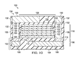
- FIG. 1F depicts the microelectronic device 100 after the etch mask is removed.
- fabrication may be substantially completed after the patterned magnetic laminate layer 126 is formed.
- additional elements of the microelectronic device 100 are formed after the patterned magnetic laminate layer 126 is formed.
- additional metal interconnect elements 130 and dielectric layers 132 are formed on the microelectronic device 100 .
- the additional metal interconnect elements 130 may be formed, for example, by electroplating copper through a plating mask.
- the additional metal interconnect elements 130 may be formed by depositing metallization layers including aluminum and forming etch masks over the metallization layers and etching the aluminum by a reactive ion etch (RIE) process using chlorine radicals.
- RIE reactive ion etch
- the additional dielectric layers 132 may be formed, for example, using methylsilsesquioxane (MSQ) in a spin-on process, or using tetraethoxysilane, also known as tetraethyl orthosilicate (TEOS), in a plasma enhanced chemical vapor deposition (PECVD) process, or using dichlorosilane in an sub-atmospheric pressure chemical vapor deposition (SACVD) process.
- MSQ methylsilsesquioxane
- PECVD plasma enhanced chemical vapor deposition
- SACVD sub-atmospheric pressure chemical vapor deposition
- the copper lines 108 , copper vias 110 and additional metal interconnect elements 130 may provide windings 134 of a solenoid inductor or a transformer around the patterned magnetic laminate layer 126 .
- the windings 134 combined with the patterned magnetic laminate layer 126 may be part of a magnetic sensor.
- FIG. 2A and FIG. 2B are cross sections of the example microelectronic device of FIG. 1A through FIG. 1G , depicted in key stages of an alternate fabrication sequence.
- the etch mask 124 is formed over the magnetic laminate layer 118 .
- the aqueous wet etch solution 128 is sprayed onto the magnetic laminate layer 118 by a spray etch tool 136 , for example an FSI Mercury Wet Process System or a Semitool Spray Acid Tool.
- the aqueous wet etch solution 128 may be at a temperature of 20° C. to 25° C., to accrue the advantages described in reference to FIG. 1C .
- Use of the spray etch tool 136 may reduce the undercut 114 and hence improve performance of the microelectronic device 100 .
- Use of the spray etch tool 136 may reduce consumption of the aqueous wet etch solution 128 and thus advantageously reduce fabrication cost of the microelectronic device 100 .
- FIG. 2A depicts the removal process partway to completion.
- FIG. 2B removal of the magnetic laminate layer 118 in the areas exposed by the etch mask 124 by the aqueous wet etch solution 128 is completed.
- the adhesion layer 116 if present, is removed by the aqueous wet etch solution 128 .
- the microelectronic device 100 may be rinsed in the spray etch tool 136 . Fabrication of the microelectronic device 100 continues as described in reference to FIG. 1E through FIG. 1G .
Abstract
A microelectronic device is formed by forming a stack of alternating layers of a magnetic material and a dielectric material. An etch mask is formed over the magnetic laminate layer. An aqueous wet etch including 5 percent to 10 percent nitric acid, 0.5 percent to 2 percent sulphuric acid, and 0.5 percent to 3 percent hydrofluoric acid is used to etch the magnetic laminate layer where exposed by the etch mask to form a patterned magnetic laminate layer. An optional adhesion layer, if present, is also removed by the aqueous wet etch solution where exposed by the etch mask. The etch mask is subsequently removed.
Description
This invention relates to the field of microelectronic devices. More particularly, this invention relates to laminated magnetic layers in microelectronic devices.
An inductor formed by planar processing includes a magnetic core layer of a laminate of alternating layers of magnetic material and dielectric, to reduce eddy current losses. The magnetic material includes at least 80 percent cobalt, at least 1 percent tantalum and at least 1 percent zirconium. Patterning the magnetic laminate layer has been problematic. Wet etch processes leave residue and degrade exposed copper interconnects. Dry etch processes such as ion milling have high manufacturing costs.
The following presents a simplified summary in order to provide a basic understanding of one or more aspects of the invention. This summary is not an extensive overview of the invention, and is neither intended to identify key or critical elements of the invention, nor to delineate the scope thereof. Rather, the primary purpose of the summary is to present some concepts of the invention in a simplified form as a prelude to a more detailed description that is presented later.
A microelectronic device containing a patterned magnetic laminate layer is formed by forming an etch mask over the magnetic laminate layer and removing the magnetic laminate layer exposed by the etch mask using an aqueous wet etch including 5 percent to 10 percent nitric acid, 0.5 percent to 2.0 percent sulphuric acid, and 0.5 percent to 3 percent hydrofluoric acid. The etch mask is subsequently removed.
The present invention is described with reference to the attached figures. The figures are not drawn to scale and they are provided merely to illustrate the invention. Several aspects of the invention are described below with reference to example applications for illustration. It should be understood that numerous specific details, relationships, and methods are set forth to provide an understanding of the invention. One skilled in the relevant art, however, will readily recognize that the invention can be practiced without one or more of the specific details or with other methods. In other instances, well-known structures or operations are not shown in detail to avoid obscuring the invention. The present invention is not limited by the illustrated ordering of acts or events, as some acts may occur in different orders and/or concurrently with other acts or events. Furthermore, not all illustrated acts or events are required to implement a methodology in accordance with the present invention.
A microelectronic device has a dielectric substrate, possibly with exposed copper interconnects. An optional adhesion layer may be formed on the substrate. A magnetic laminate layer of alternating layers of magnetic material and dielectric material, with at least two layers of the magnetic material and at least one layer of the dielectric material, is formed over the substrate. An etch mask is formed over the magnetic laminate layer to cover an area for a patterned magnetic laminate layer. The magnetic laminate layer is removed in areas exposed by the etch mask using an aqueous wet etch. The wet etch includes 5 percent to 10 percent nitric acid, 0.5 percent to 2.0 percent sulphuric acid, and 0.5 percent to 3 percent hydrofluoric acid. The wet etch may be, for example, an immersion process or a spray process. The patterned magnetic laminate layer may be part of an inductor, a transformer, a magnetic sensor, or other magnetic device, which may be formed by planar processing.
The substrate 102 may contain metal interconnects 106. The metal interconnects 106 may include copper lines 108 and/or copper vias 110 formed by masked electroplating. Some of the metal interconnects 106, for example the copper vias 110, may extend to a top surface 112 of the substrate 102.
An optional adhesion layer 116 may be formed on the top surface 112. The adhesion layer 116 may be, for example, 1 nanometer to 1000 nanometers thick, and may include, for example, titanium, titanium nitride, tantalum, and/or tantalum nitride. The adhesion layer 116 may be formed by sputtering or reactive sputtering.
Referring to FIG. 1B , a magnetic laminate layer 118 is formed over the substrate 102, on the adhesion layer 116 if present. The magnetic laminate layer 118 includes layers of magnetic material 120 alternating with layers of dielectric material 122, with at least two layers of the magnetic material 120 and at least one layer of the dielectric material 122. The layers of dielectric material 122 may reduce eddy currents in the magnetic laminate layer 118 during operation of the microelectronic device 100. The magnetic laminate layer 118 may include at least five layers of the magnetic material 120 and at least five layers of the dielectric material 122. The magnetic material 120 may include, for example, at least 80 percent cobalt, at least 1 percent tantalum and at least 1 percent zirconium. The layers of the magnetic material 120 may be formed by sputtering, and may be, for example, 0.5 microns to 1.5 microns thick. Other compositions of the magnetic material 120 are within the scope of the instant example. The dielectric material 122 may be primarily aluminum nitride, formed by reactive sputtering. Forming both the layers of the magnetic material 120 and the layers of dielectric material 122 by sputtering processes may improve fabrication throughput of the microelectronic device 100 and thus advantageously reduce manufacturing cost. The layers of the dielectric material 122 may be, for example, 1 nanometer to 1000 nanometers thick. Other compositions of the dielectric material 122 are within the scope of the instant example.
An etch mask 124 is formed over the magnetic laminate layer 118 so as to cover an area for the patterned magnetic laminate layer 126 and expose the magnetic laminate layer 118 outside the area for the patterned magnetic laminate layer 126. The etch mask 124 may include photoresist formed by a photolithographic process. The etch mask 124 may further include an anti-reflection layer, not shown in FIG. 1B .
Referring to FIG. 1C , the magnetic laminate layer 118 is removed in the areas exposed by the etch mask 124 by immersing the magnetic laminate layer 118 in an aqueous wet etch solution 128. FIG. 1C depicts the removal process partway to completion. The aqueous wet etch solution 128 comprises 5 percent to 10 percent nitric acid, 0.5 percent to 2.0 percent sulphuric acid, 0.5 percent to 3 percent hydrofluoric acid, and at least 80 percent deionized water (DI H2O). Inclusion other materials such as surfactants which do not directly remove the magnetic laminate layer 118 is within the scope of the instant example. The nitric acid is effective for removing the layers of the magnetic material 120 and the layers of the dielectric material 122. Using a concentration of the nitric acid less than 5 percent disadvantageously reduces throughput of the removal process and may unacceptably increase manufacturing cost of the microelectronic device 100. Using a concentration of the nitric acid above 10 percent disadvantageously degrades the etch mask 124 and may unacceptably increase undercut 114 of the patterned magnetic laminate layer 126. The sulphuric acid is effective for reducing degradation of the exposed copper vias 110. Concentrations of the sulphuric acid below 0.5 percent and above 2 percent are not effective for reducing degradation of the exposed copper vias 110. The hydrofluoric acid is effective for removing the adhesion layer 116. Using a concentration of the hydrofluoric acid below 0.5 percent is not effective for removing the adhesion layer 116. Using a concentration of the hydrofluoric acid above 3 percent disadvantageously reduces control of overetch of the dielectric material 104 in the substrate 102. The aqueous wet etch solution 128 may be at a temperature of 20° C. to 25° C. Maintaining the aqueous wet etch solution 128 at a temperature below 20° C. may require cooling the aqueous wet etch solution 128, disadvantageously increasing complexity and cost of equipment containing the aqueous wet etch solution 128. Maintaining the aqueous wet etch solution 128 at a temperature above 25° C. disadvantageously increases difficulty of determining completion of the removal of the magnetic laminate layer 118 while maintaining overetch dielectric material 104 at a desired value.
Referring to FIG. 1D , removal of the magnetic laminate layer 118 in the areas exposed by the etch mask 124 by the aqueous wet etch solution 128 is completed. The adhesion layer 116, if present, is removed by the aqueous wet etch solution 128. The concentration of the hydrofluoric acid in the aqueous wet etch solution 128 may be selected to provide an acceptable overetch of the dielectric material 104 in the substrate 102. The microelectronic device 100 is subsequently removed from the aqueous wet etch solution 128 and rinsed.
Referring to FIG. 1E , the etch mask 124 is removed. The etch mask 124 may be removed, for example, by immersion in a solvent mixture and/or by an ash process. FIG. 1E depicts the removal process partway to completion.
Referring to FIG. 1G , additional metal interconnect elements 130 and dielectric layers 132 are formed on the microelectronic device 100. The additional metal interconnect elements 130 may be formed, for example, by electroplating copper through a plating mask. Alternatively, the additional metal interconnect elements 130 may be formed by depositing metallization layers including aluminum and forming etch masks over the metallization layers and etching the aluminum by a reactive ion etch (RIE) process using chlorine radicals. The additional dielectric layers 132 may be formed, for example, using methylsilsesquioxane (MSQ) in a spin-on process, or using tetraethoxysilane, also known as tetraethyl orthosilicate (TEOS), in a plasma enhanced chemical vapor deposition (PECVD) process, or using dichlorosilane in an sub-atmospheric pressure chemical vapor deposition (SACVD) process. The copper lines 108, copper vias 110 and additional metal interconnect elements 130 may provide windings 134 of a solenoid inductor or a transformer around the patterned magnetic laminate layer 126. The windings 134 combined with the patterned magnetic laminate layer 126 may be part of a magnetic sensor.
Referring to FIG. 2B , removal of the magnetic laminate layer 118 in the areas exposed by the etch mask 124 by the aqueous wet etch solution 128 is completed. The adhesion layer 116, if present, is removed by the aqueous wet etch solution 128. The microelectronic device 100 may be rinsed in the spray etch tool 136. Fabrication of the microelectronic device 100 continues as described in reference to FIG. 1E through FIG. 1G .
While various embodiments of the present invention have been described above, it should be understood that they have been presented by way of example only and not limitation. Numerous changes to the disclosed embodiments can be made in accordance with the disclosure herein without departing from the spirit or scope of the invention. Thus, the breadth and scope of the present invention should not be limited by any of the above described embodiments. Rather, the scope of the invention should be defined in accordance with the following claims and their equivalents.
Claims (18)
1. A method of forming a microelectronic device, comprising the steps:
providing a substrate comprising a dielectric material;
forming a magnetic laminate layer over the substrate, the magnetic laminate layer comprising at least two layers of magnetic material alternating with at least one layer of dielectric material, wherein the magnetic material in the magnetic laminate layer includes at least 80 percent cobalt, at least 1 percent tantalum and at least 1 percent zirconium;
forming an etch mask over the magnetic laminate layer;
removing the magnetic laminate layer in areas exposed by the etch mask using an aqueous wet etch solution comprising nitric acid, sulphuric acid, hydrofluoric acid, and deionized water, to form a patterned magnetic laminate layer; and
subsequently removing the etch mask.
2. The method of claim 1 , wherein removing the magnetic laminate layer is performed by immersing the magnetic laminate layer in the aqueous wet etch solution.
3. The method of claim 1 , wherein removing the magnetic laminate layer is performed by spraying the aqueous wet etch solution onto the magnetic laminate layer.
4. The method of claim 1 , wherein removing the magnetic laminate layer is performed with the aqueous wet etch solution at a temperature of 20° C. to 25° C.
5. The method of claim 1 , wherein each layer of the magnetic material in the magnetic laminate layer is 0.5 microns to 1.5 microns thick.
6. The method of claim 1 , wherein the dielectric material in the magnetic laminate layer includes aluminum nitride.
7. The method of claim 1 , wherein each layer of the dielectric material in the magnetic laminate layer is 1 nanometer to 1000 nanometers thick.
8. The method of claim 1 , wherein the magnetic laminate layer includes at least five layers of the magnetic material and at least five layers of the dielectric material.
9. The method of claim 1 , wherein the dielectric material in the substrate includes silicon dioxide.
10. The method of claim 1 , wherein the substrate contains a metal interconnect comprising copper.
11. The method of claim 10 , wherein the metal interconnect comprising copper extends to a top surface of the substrate.
12. The method of claim 1 , comprising forming an adhesion layer over the substrate before forming the magnetic laminate layer, and wherein the adhesion layer is removed by the aqueous wet etch solution.
13. The method of claim 12 , wherein the adhesion layer comprises a material selected from the group consisting of titanium, titanium nitride, tantalum and tantalum nitride.
14. The method of claim 1 , comprising forming a dielectric layer over the patterned magnetic laminate layer, after removing the etch mask.
15. The method of claim 14 , comprising forming metal interconnect elements on the microelectronic device, after removing the etch mask.
16. The method of claim 15 , wherein the metal interconnect elements and the patterned magnetic laminate layer are parts of a component selected from the group consisting of a solenoid inductor, a transformer and a magnetic sensor.
17. A method of forming a microelectronic device, comprising the steps:
providing a substrate comprising a dielectric material, the substrate containing an interconnect comprising copper extending to a top surface of the substrate;
forming an adhesion layer over the substrate, the adhesion layer comprising a material selected from the group consisting of titanium, titanium nitride, tantalum and tantalum nitride;
forming a magnetic laminate layer over the substrate, the magnetic laminate layer comprising at least two layers of magnetic material 0.5 microns to 1.5 microns thick alternating with at least one layer of dielectric material 1 nanometer to 1000 nanometers thick, the magnetic material including at least 80 percent cobalt, at least 1 percent tantalum and at least 1 percent zirconium, and the dielectric material including aluminum nitride;
forming an etch mask over the magnetic laminate layer;
removing the magnetic laminate layer and the adhesion layer in areas exposed by the etch mask by immersing the magnetic laminate layer in an aqueous wet etch solution comprising 5 percent to 10 percent nitric acid, 0.5 percent to 2.0 percent sulphuric acid, 0.5 percent to 3 percent hydrofluoric acid, and at least 80 percent deionized water, to form a patterned magnetic laminate layer, the aqueous wet etch solution being at a temperature of 20° C. to 25° C.;
subsequently removing the etch mask;
forming a dielectric layer over the patterned magnetic laminate layer after removing the etch mask; and
forming metal interconnect elements on the microelectronic device after removing the etch mask.
18. A method of forming a microelectronic device, comprising the steps:
providing a substrate comprising a dielectric material;
forming an adhesion layer over the substrate;
forming a magnetic laminate layer over the substrate, the magnetic laminate layer comprising at least two layers of magnetic material 0.5 microns to 1.5 microns thick alternating with at least one layer of dielectric material 1 nanometer to 1000 nanometers thick, the magnetic material including at least 80 percent cobalt, at least 1 percent tantalum and at least 1 percent zirconium, and the dielectric material including aluminum nitride;
forming an etch mask over the magnetic laminate layer;
removing the magnetic laminate layer and the adhesion layer in areas exposed by the etch mask by immersing the magnetic laminate layer in an aqueous wet etch solution comprising 5 percent to 10 percent nitric acid, 0.5 percent to 2 percent sulphuric acid, 0.5 percent to 3 percent hydrofluoric acid, and at least 80 percent deionized water, to form a patterned magnetic laminate layer, the aqueous wet etch solution being at a temperature of 20° C. to 25° C.; and
subsequently removing the etch mask.
Priority Applications (1)
| Application Number | Priority Date | Filing Date | Title |
|---|---|---|---|
| US14/715,546 US9633866B2 (en) | 2015-05-18 | 2015-05-18 | Method for patterning of laminated magnetic layer |
Applications Claiming Priority (1)
| Application Number | Priority Date | Filing Date | Title |
|---|---|---|---|
| US14/715,546 US9633866B2 (en) | 2015-05-18 | 2015-05-18 | Method for patterning of laminated magnetic layer |
Publications (2)
| Publication Number | Publication Date |
|---|---|
| US20160343586A1 US20160343586A1 (en) | 2016-11-24 |
| US9633866B2 true US9633866B2 (en) | 2017-04-25 |
Family
ID=57324550
Family Applications (1)
| Application Number | Title | Priority Date | Filing Date |
|---|---|---|---|
| US14/715,546 Active 2035-05-27 US9633866B2 (en) | 2015-05-18 | 2015-05-18 | Method for patterning of laminated magnetic layer |
Country Status (1)
| Country | Link |
|---|---|
| US (1) | US9633866B2 (en) |
Cited By (1)
| Publication number | Priority date | Publication date | Assignee | Title |
|---|---|---|---|---|
| US10049802B2 (en) * | 2016-10-11 | 2018-08-14 | International Business Machines Corporation | Patterning magnetic films using self-stop electro-etching |
Families Citing this family (1)
| Publication number | Priority date | Publication date | Assignee | Title |
|---|---|---|---|---|
| US20180206334A1 (en) * | 2017-01-16 | 2018-07-19 | Innolux Corporation | Metal-laminated structure and high-frequency device comprising the same |
Citations (6)
| Publication number | Priority date | Publication date | Assignee | Title |
|---|---|---|---|---|
| US20010006246A1 (en) * | 1998-06-25 | 2001-07-05 | Kwag Gyu-Hwan | Method of manufacturing semiconductor devices, etching composition for manufacturing semiconductor devices, and semiconductor devices made using the method |
| US20020036315A1 (en) * | 2000-09-26 | 2002-03-28 | Hideaki Adachi | Magnetoresistive element and magnetoresistive device using the same |
| US20020090534A1 (en) * | 2001-01-09 | 2002-07-11 | Hitachi Metals, Ltd. | Magneto resistive sensor |
| US20020132136A1 (en) * | 2001-03-15 | 2002-09-19 | Roshen Waseem A. | Low loss, high frequency composite magnetic material and methods of making the same |
| US20060014305A1 (en) * | 2004-07-14 | 2006-01-19 | Lee Gill Y | MTJ patterning using free layer wet etching and lift off techniques |
| US20100120248A1 (en) * | 2007-01-22 | 2010-05-13 | Gp Solar Gmbh | Etching solution and etching method |
-
2015
- 2015-05-18 US US14/715,546 patent/US9633866B2/en active Active
Patent Citations (6)
| Publication number | Priority date | Publication date | Assignee | Title |
|---|---|---|---|---|
| US20010006246A1 (en) * | 1998-06-25 | 2001-07-05 | Kwag Gyu-Hwan | Method of manufacturing semiconductor devices, etching composition for manufacturing semiconductor devices, and semiconductor devices made using the method |
| US20020036315A1 (en) * | 2000-09-26 | 2002-03-28 | Hideaki Adachi | Magnetoresistive element and magnetoresistive device using the same |
| US20020090534A1 (en) * | 2001-01-09 | 2002-07-11 | Hitachi Metals, Ltd. | Magneto resistive sensor |
| US20020132136A1 (en) * | 2001-03-15 | 2002-09-19 | Roshen Waseem A. | Low loss, high frequency composite magnetic material and methods of making the same |
| US20060014305A1 (en) * | 2004-07-14 | 2006-01-19 | Lee Gill Y | MTJ patterning using free layer wet etching and lift off techniques |
| US20100120248A1 (en) * | 2007-01-22 | 2010-05-13 | Gp Solar Gmbh | Etching solution and etching method |
Cited By (1)
| Publication number | Priority date | Publication date | Assignee | Title |
|---|---|---|---|---|
| US10049802B2 (en) * | 2016-10-11 | 2018-08-14 | International Business Machines Corporation | Patterning magnetic films using self-stop electro-etching |
Also Published As
| Publication number | Publication date |
|---|---|
| US20160343586A1 (en) | 2016-11-24 |
Similar Documents
| Publication | Publication Date | Title |
|---|---|---|
| US9852916B2 (en) | Single platform, multiple cycle spacer deposition and etch | |
| US20160351798A1 (en) | MTJ Etching with Improved Uniformity and Profile by Adding Passivation Step | |
| US8222160B2 (en) | Metal containing sacrifice material and method of damascene wiring formation | |
| US7122484B2 (en) | Process for removing organic materials during formation of a metal interconnect | |
| US20050260856A1 (en) | Methods of fabricating a semiconductor device using an organic compound and fluoride-based buffered solution | |
| CN103165414B (en) | The method forming the pattern for semiconductor device | |
| KR101570295B1 (en) | Semiconductor devices, methods of manufacture thereof, and methods of forming conductive features | |
| US20160043046A1 (en) | Etching of under bump metallization layer and resulting device | |
| US9633866B2 (en) | Method for patterning of laminated magnetic layer | |
| CN101840859A (en) | Manufacturing method of semiconductor component | |
| US10354913B2 (en) | Chemical clean of semiconductor device | |
| US20120315755A1 (en) | Copper interconnect with metal hardmask removal | |
| US20180358163A1 (en) | Method to form magnetic core for integrated magnetic devices | |
| US9123662B2 (en) | Reducing defects in patterning processes | |
| US6740471B1 (en) | Photoresist adhesion improvement on metal layer after photoresist rework by extra N2O treatment | |
| US7879533B2 (en) | Etching residue removal method and semiconductor device fabrication method using this method | |
| JP2009290040A (en) | Method for manufacturing semiconductor integrated circuit device | |
| US20130260571A1 (en) | Treatment liquid for inhibiting pattern collapse in microstructure and method of manufacturing microstructure using the same | |
| US9922874B2 (en) | Methods of enhancing polymer adhesion to copper | |
| US20100163294A1 (en) | Method for forming metal line of semiconductor device | |
| Kuo et al. | C4 Compatible Ultra-Thick Cu On-chip Magnetic Inductor Architecture Integrated with Advanced Polymer/Cu Planarization Process | |
| US6495472B2 (en) | Method for avoiding erosion of conductor structure during removing etching residues | |
| KR100884980B1 (en) | Manufacturing method of semiconductor device | |
| US20230317512A1 (en) | Method for fabricating semiconductor device and reworking process | |
| US20230154753A1 (en) | Patterned Semiconductor Device and Method |
Legal Events
| Date | Code | Title | Description |
|---|---|---|---|
| AS | Assignment |
Owner name: TEXAS INSTRUMENTS INCORPORATED, TEXAS Free format text: ASSIGNMENT OF ASSIGNORS INTEREST;ASSIGNOR:SHULVER, BYRON J R;REEL/FRAME:035663/0558 Effective date: 20150508 |
|
| STCF | Information on status: patent grant |
Free format text: PATENTED CASE |
|
| MAFP | Maintenance fee payment |
Free format text: PAYMENT OF MAINTENANCE FEE, 4TH YEAR, LARGE ENTITY (ORIGINAL EVENT CODE: M1551); ENTITY STATUS OF PATENT OWNER: LARGE ENTITY Year of fee payment: 4 |