US9646869B2 - Semiconductor devices including a diode structure over a conductive strap and methods of forming such semiconductor devices - Google Patents
Semiconductor devices including a diode structure over a conductive strap and methods of forming such semiconductor devices Download PDFInfo
- Publication number
- US9646869B2 US9646869B2 US12/715,743 US71574310A US9646869B2 US 9646869 B2 US9646869 B2 US 9646869B2 US 71574310 A US71574310 A US 71574310A US 9646869 B2 US9646869 B2 US 9646869B2
- Authority
- US
- United States
- Prior art keywords
- doped region
- diode
- semiconductor substrate
- conductive material
- over
- Prior art date
- Legal status (The legal status is an assumption and is not a legal conclusion. Google has not performed a legal analysis and makes no representation as to the accuracy of the status listed.)
- Active, expires
Links
- 239000004065 semiconductor Substances 0.000 title claims abstract description 173
- 238000000034 method Methods 0.000 title abstract description 59
- 239000000463 material Substances 0.000 claims abstract description 236
- 239000004020 conductor Substances 0.000 claims abstract description 90
- 239000012212 insulator Substances 0.000 claims abstract description 48
- 239000002210 silicon-based material Substances 0.000 claims abstract description 34
- 229910021419 crystalline silicon Inorganic materials 0.000 claims abstract description 32
- 239000000758 substrate Substances 0.000 claims description 119
- 239000002019 doping agent Substances 0.000 claims description 15
- 229910021417 amorphous silicon Inorganic materials 0.000 claims description 7
- 229910052732 germanium Inorganic materials 0.000 claims description 7
- GNPVGFCGXDBREM-UHFFFAOYSA-N germanium atom Chemical compound [Ge] GNPVGFCGXDBREM-UHFFFAOYSA-N 0.000 claims description 7
- 230000008878 coupling Effects 0.000 claims description 3
- 238000010168 coupling process Methods 0.000 claims description 3
- 238000005859 coupling reaction Methods 0.000 claims description 3
- 239000000853 adhesive Substances 0.000 claims 8
- 230000001070 adhesive effect Effects 0.000 claims 8
- 239000007772 electrode material Substances 0.000 claims 1
- 235000012431 wafers Nutrition 0.000 description 42
- 239000007789 gas Substances 0.000 description 25
- NRTOMJZYCJJWKI-UHFFFAOYSA-N Titanium nitride Chemical compound [Ti]#N NRTOMJZYCJJWKI-UHFFFAOYSA-N 0.000 description 23
- 239000002243 precursor Substances 0.000 description 23
- 150000002500 ions Chemical class 0.000 description 19
- 230000008569 process Effects 0.000 description 18
- 229910021420 polycrystalline silicon Inorganic materials 0.000 description 17
- 229920005591 polysilicon Polymers 0.000 description 17
- 238000000151 deposition Methods 0.000 description 15
- 238000005229 chemical vapour deposition Methods 0.000 description 12
- 238000001020 plasma etching Methods 0.000 description 12
- 238000000231 atomic layer deposition Methods 0.000 description 11
- 238000000059 patterning Methods 0.000 description 11
- RTAQQCXQSZGOHL-UHFFFAOYSA-N Titanium Chemical compound [Ti] RTAQQCXQSZGOHL-UHFFFAOYSA-N 0.000 description 10
- 238000004519 manufacturing process Methods 0.000 description 10
- 239000010936 titanium Substances 0.000 description 10
- 229910052719 titanium Inorganic materials 0.000 description 10
- YCKRFDGAMUMZLT-UHFFFAOYSA-N Fluorine atom Chemical compound [F] YCKRFDGAMUMZLT-UHFFFAOYSA-N 0.000 description 9
- 229910052731 fluorine Inorganic materials 0.000 description 9
- 239000011737 fluorine Substances 0.000 description 9
- 238000005240 physical vapour deposition Methods 0.000 description 9
- 239000000203 mixture Substances 0.000 description 8
- TXEYQDLBPFQVAA-UHFFFAOYSA-N tetrafluoromethane Chemical compound FC(F)(F)F TXEYQDLBPFQVAA-UHFFFAOYSA-N 0.000 description 8
- 229910052721 tungsten Inorganic materials 0.000 description 7
- 239000010937 tungsten Substances 0.000 description 7
- 229910052751 metal Inorganic materials 0.000 description 6
- 239000002184 metal Substances 0.000 description 6
- 238000012545 processing Methods 0.000 description 6
- -1 tungsten nitride Chemical class 0.000 description 6
- XUIMIQQOPSSXEZ-UHFFFAOYSA-N Silicon Chemical compound [Si] XUIMIQQOPSSXEZ-UHFFFAOYSA-N 0.000 description 5
- 230000006870 function Effects 0.000 description 5
- 239000007943 implant Substances 0.000 description 5
- 229910052710 silicon Inorganic materials 0.000 description 5
- 239000010703 silicon Substances 0.000 description 5
- 238000012546 transfer Methods 0.000 description 5
- WKBOTKDWSSQWDR-UHFFFAOYSA-N Bromine atom Chemical compound [Br] WKBOTKDWSSQWDR-UHFFFAOYSA-N 0.000 description 4
- OKTJSMMVPCPJKN-UHFFFAOYSA-N Carbon Chemical compound [C] OKTJSMMVPCPJKN-UHFFFAOYSA-N 0.000 description 4
- ZAMOUSCENKQFHK-UHFFFAOYSA-N Chlorine atom Chemical compound [Cl] ZAMOUSCENKQFHK-UHFFFAOYSA-N 0.000 description 4
- VYPSYNLAJGMNEJ-UHFFFAOYSA-N Silicium dioxide Chemical compound O=[Si]=O VYPSYNLAJGMNEJ-UHFFFAOYSA-N 0.000 description 4
- 229910003481 amorphous carbon Inorganic materials 0.000 description 4
- QVGXLLKOCUKJST-UHFFFAOYSA-N atomic oxygen Chemical compound [O] QVGXLLKOCUKJST-UHFFFAOYSA-N 0.000 description 4
- 230000015572 biosynthetic process Effects 0.000 description 4
- GDTBXPJZTBHREO-UHFFFAOYSA-N bromine Substances BrBr GDTBXPJZTBHREO-UHFFFAOYSA-N 0.000 description 4
- 229910052794 bromium Inorganic materials 0.000 description 4
- 229910052799 carbon Inorganic materials 0.000 description 4
- 150000004770 chalcogenides Chemical class 0.000 description 4
- 239000000460 chlorine Substances 0.000 description 4
- 229910052801 chlorine Inorganic materials 0.000 description 4
- 239000003989 dielectric material Substances 0.000 description 4
- 239000001301 oxygen Substances 0.000 description 4
- 229910052760 oxygen Inorganic materials 0.000 description 4
- 229920002120 photoresistant polymer Polymers 0.000 description 4
- WFKWXMTUELFFGS-UHFFFAOYSA-N tungsten Chemical compound [W] WFKWXMTUELFFGS-UHFFFAOYSA-N 0.000 description 4
- 238000007796 conventional method Methods 0.000 description 3
- 238000005516 engineering process Methods 0.000 description 3
- 238000005530 etching Methods 0.000 description 3
- 239000011521 glass Substances 0.000 description 3
- 230000008018 melting Effects 0.000 description 3
- 238000002844 melting Methods 0.000 description 3
- 230000004048 modification Effects 0.000 description 3
- 238000012986 modification Methods 0.000 description 3
- 150000004767 nitrides Chemical class 0.000 description 3
- 238000000623 plasma-assisted chemical vapour deposition Methods 0.000 description 3
- 229910021341 titanium silicide Inorganic materials 0.000 description 3
- WQJQOUPTWCFRMM-UHFFFAOYSA-N tungsten disilicide Chemical compound [Si]#[W]#[Si] WQJQOUPTWCFRMM-UHFFFAOYSA-N 0.000 description 3
- 229910021342 tungsten silicide Inorganic materials 0.000 description 3
- XKRFYHLGVUSROY-UHFFFAOYSA-N Argon Chemical compound [Ar] XKRFYHLGVUSROY-UHFFFAOYSA-N 0.000 description 2
- 239000005380 borophosphosilicate glass Substances 0.000 description 2
- 239000005388 borosilicate glass Substances 0.000 description 2
- 230000008859 change Effects 0.000 description 2
- 230000003247 decreasing effect Effects 0.000 description 2
- 230000008021 deposition Effects 0.000 description 2
- 238000010586 diagram Methods 0.000 description 2
- 239000001257 hydrogen Substances 0.000 description 2
- 229910052739 hydrogen Inorganic materials 0.000 description 2
- 239000012535 impurity Substances 0.000 description 2
- 238000011065 in-situ storage Methods 0.000 description 2
- 238000002955 isolation Methods 0.000 description 2
- 229910044991 metal oxide Inorganic materials 0.000 description 2
- 150000004706 metal oxides Chemical class 0.000 description 2
- 239000012782 phase change material Substances 0.000 description 2
- 239000005360 phosphosilicate glass Substances 0.000 description 2
- 229910021332 silicide Inorganic materials 0.000 description 2
- FVBUAEGBCNSCDD-UHFFFAOYSA-N silicide(4-) Chemical compound [Si-4] FVBUAEGBCNSCDD-UHFFFAOYSA-N 0.000 description 2
- 239000000377 silicon dioxide Substances 0.000 description 2
- 235000012239 silicon dioxide Nutrition 0.000 description 2
- 239000007784 solid electrolyte Substances 0.000 description 2
- 229910052715 tantalum Inorganic materials 0.000 description 2
- GUVRBAGPIYLISA-UHFFFAOYSA-N tantalum atom Chemical compound [Ta] GUVRBAGPIYLISA-UHFFFAOYSA-N 0.000 description 2
- 230000000007 visual effect Effects 0.000 description 2
- VHUUQVKOLVNVRT-UHFFFAOYSA-N Ammonium hydroxide Chemical compound [NH4+].[OH-] VHUUQVKOLVNVRT-UHFFFAOYSA-N 0.000 description 1
- JBRZTFJDHDCESZ-UHFFFAOYSA-N AsGa Chemical compound [As]#[Ga] JBRZTFJDHDCESZ-UHFFFAOYSA-N 0.000 description 1
- ZOXJGFHDIHLPTG-UHFFFAOYSA-N Boron Chemical compound [B] ZOXJGFHDIHLPTG-UHFFFAOYSA-N 0.000 description 1
- QPLDLSVMHZLSFG-UHFFFAOYSA-N Copper oxide Chemical compound [Cu]=O QPLDLSVMHZLSFG-UHFFFAOYSA-N 0.000 description 1
- 239000005751 Copper oxide Substances 0.000 description 1
- KRHYYFGTRYWZRS-UHFFFAOYSA-N Fluorane Chemical compound F KRHYYFGTRYWZRS-UHFFFAOYSA-N 0.000 description 1
- 229910001218 Gallium arsenide Inorganic materials 0.000 description 1
- UFHFLCQGNIYNRP-UHFFFAOYSA-N Hydrogen Chemical compound [H][H] UFHFLCQGNIYNRP-UHFFFAOYSA-N 0.000 description 1
- GPXJNWSHGFTCBW-UHFFFAOYSA-N Indium phosphide Chemical compound [In]#P GPXJNWSHGFTCBW-UHFFFAOYSA-N 0.000 description 1
- GWEVSGVZZGPLCZ-UHFFFAOYSA-N Titan oxide Chemical compound O=[Ti]=O GWEVSGVZZGPLCZ-UHFFFAOYSA-N 0.000 description 1
- 230000003213 activating effect Effects 0.000 description 1
- 230000004913 activation Effects 0.000 description 1
- 238000001994 activation Methods 0.000 description 1
- 229910052782 aluminium Inorganic materials 0.000 description 1
- XAGFODPZIPBFFR-UHFFFAOYSA-N aluminium Chemical compound [Al] XAGFODPZIPBFFR-UHFFFAOYSA-N 0.000 description 1
- 229910052787 antimony Inorganic materials 0.000 description 1
- WATWJIUSRGPENY-UHFFFAOYSA-N antimony atom Chemical compound [Sb] WATWJIUSRGPENY-UHFFFAOYSA-N 0.000 description 1
- 229910052786 argon Inorganic materials 0.000 description 1
- 229910052785 arsenic Inorganic materials 0.000 description 1
- RQNWIZPPADIBDY-UHFFFAOYSA-N arsenic atom Chemical compound [As] RQNWIZPPADIBDY-UHFFFAOYSA-N 0.000 description 1
- 229910052796 boron Inorganic materials 0.000 description 1
- 210000004556 brain Anatomy 0.000 description 1
- 230000001413 cellular effect Effects 0.000 description 1
- 239000000919 ceramic Substances 0.000 description 1
- 238000003776 cleavage reaction Methods 0.000 description 1
- 238000004581 coalescence Methods 0.000 description 1
- 239000011248 coating agent Substances 0.000 description 1
- 238000000576 coating method Methods 0.000 description 1
- 230000000295 complement effect Effects 0.000 description 1
- 229910000431 copper oxide Inorganic materials 0.000 description 1
- 230000006378 damage Effects 0.000 description 1
- 230000001419 dependent effect Effects 0.000 description 1
- 238000009792 diffusion process Methods 0.000 description 1
- 230000000694 effects Effects 0.000 description 1
- 230000005611 electricity Effects 0.000 description 1
- 238000007667 floating Methods 0.000 description 1
- 238000000227 grinding Methods 0.000 description 1
- 238000010438 heat treatment Methods 0.000 description 1
- BHEPBYXIRTUNPN-UHFFFAOYSA-N hydridophosphorus(.) (triplet) Chemical compound [PH] BHEPBYXIRTUNPN-UHFFFAOYSA-N 0.000 description 1
- 229910000040 hydrogen fluoride Inorganic materials 0.000 description 1
- 238000002513 implantation Methods 0.000 description 1
- 238000005468 ion implantation Methods 0.000 description 1
- 238000004518 low pressure chemical vapour deposition Methods 0.000 description 1
- 239000007769 metal material Substances 0.000 description 1
- 150000002739 metals Chemical class 0.000 description 1
- 229910021421 monocrystalline silicon Inorganic materials 0.000 description 1
- 230000006855 networking Effects 0.000 description 1
- 229910000480 nickel oxide Inorganic materials 0.000 description 1
- 229910052756 noble gas Inorganic materials 0.000 description 1
- 150000002835 noble gases Chemical class 0.000 description 1
- QGLKJKCYBOYXKC-UHFFFAOYSA-N nonaoxidotritungsten Chemical compound O=[W]1(=O)O[W](=O)(=O)O[W](=O)(=O)O1 QGLKJKCYBOYXKC-UHFFFAOYSA-N 0.000 description 1
- GNRSAWUEBMWBQH-UHFFFAOYSA-N oxonickel Chemical compound [Ni]=O GNRSAWUEBMWBQH-UHFFFAOYSA-N 0.000 description 1
- BPUBBGLMJRNUCC-UHFFFAOYSA-N oxygen(2-);tantalum(5+) Chemical compound [O-2].[O-2].[O-2].[O-2].[O-2].[Ta+5].[Ta+5] BPUBBGLMJRNUCC-UHFFFAOYSA-N 0.000 description 1
- 230000008707 rearrangement Effects 0.000 description 1
- 229910052594 sapphire Inorganic materials 0.000 description 1
- 239000010980 sapphire Substances 0.000 description 1
- 230000007017 scission Effects 0.000 description 1
- 229910052814 silicon oxide Inorganic materials 0.000 description 1
- 238000004528 spin coating Methods 0.000 description 1
- 239000000126 substance Substances 0.000 description 1
- MZLGASXMSKOWSE-UHFFFAOYSA-N tantalum nitride Chemical compound [Ta]#N MZLGASXMSKOWSE-UHFFFAOYSA-N 0.000 description 1
- 229910001936 tantalum oxide Inorganic materials 0.000 description 1
- 238000005979 thermal decomposition reaction Methods 0.000 description 1
- 230000003685 thermal hair damage Effects 0.000 description 1
- OGIDPMRJRNCKJF-UHFFFAOYSA-N titanium oxide Inorganic materials [Ti]=O OGIDPMRJRNCKJF-UHFFFAOYSA-N 0.000 description 1
- 229910052723 transition metal Inorganic materials 0.000 description 1
- 150000003624 transition metals Chemical class 0.000 description 1
- 229910001930 tungsten oxide Inorganic materials 0.000 description 1
- 238000001039 wet etching Methods 0.000 description 1
- 229910052727 yttrium Inorganic materials 0.000 description 1
Images


Classifications
-
- H—ELECTRICITY
- H01—ELECTRIC ELEMENTS
- H01L—SEMICONDUCTOR DEVICES NOT COVERED BY CLASS H10
- H01L21/00—Processes or apparatus adapted for the manufacture or treatment of semiconductor or solid state devices or of parts thereof
- H01L21/70—Manufacture or treatment of devices consisting of a plurality of solid state components formed in or on a common substrate or of parts thereof; Manufacture of integrated circuit devices or of parts thereof
- H01L21/71—Manufacture of specific parts of devices defined in group H01L21/70
- H01L21/76—Making of isolation regions between components
- H01L21/762—Dielectric regions, e.g. EPIC dielectric isolation, LOCOS; Trench refilling techniques, SOI technology, use of channel stoppers
-
- H—ELECTRICITY
- H01—ELECTRIC ELEMENTS
- H01L—SEMICONDUCTOR DEVICES NOT COVERED BY CLASS H10
- H01L29/00—Semiconductor devices adapted for rectifying, amplifying, oscillating or switching, or capacitors or resistors with at least one potential-jump barrier or surface barrier, e.g. PN junction depletion layer or carrier concentration layer; Details of semiconductor bodies or of electrodes thereof ; Multistep manufacturing processes therefor
- H01L29/66—Types of semiconductor device ; Multistep manufacturing processes therefor
- H01L29/86—Types of semiconductor device ; Multistep manufacturing processes therefor controllable only by variation of the electric current supplied, or only the electric potential applied, to one or more of the electrodes carrying the current to be rectified, amplified, oscillated or switched
- H01L29/861—Diodes
-
- H—ELECTRICITY
- H10—SEMICONDUCTOR DEVICES; ELECTRIC SOLID-STATE DEVICES NOT OTHERWISE PROVIDED FOR
- H10B—ELECTRONIC MEMORY DEVICES
- H10B63/00—Resistance change memory devices, e.g. resistive RAM [ReRAM] devices
- H10B63/20—Resistance change memory devices, e.g. resistive RAM [ReRAM] devices comprising selection components having two electrodes, e.g. diodes
-
- H—ELECTRICITY
- H10—SEMICONDUCTOR DEVICES; ELECTRIC SOLID-STATE DEVICES NOT OTHERWISE PROVIDED FOR
- H10B—ELECTRONIC MEMORY DEVICES
- H10B63/00—Resistance change memory devices, e.g. resistive RAM [ReRAM] devices
- H10B63/30—Resistance change memory devices, e.g. resistive RAM [ReRAM] devices comprising selection components having three or more electrodes, e.g. transistors
-
- H—ELECTRICITY
- H10—SEMICONDUCTOR DEVICES; ELECTRIC SOLID-STATE DEVICES NOT OTHERWISE PROVIDED FOR
- H10N—ELECTRIC SOLID-STATE DEVICES NOT OTHERWISE PROVIDED FOR
- H10N70/00—Solid-state devices without a potential-jump barrier or surface barrier, and specially adapted for rectifying, amplifying, oscillating or switching
- H10N70/011—Manufacture or treatment of multistable switching devices
- H10N70/061—Patterning of the switching material
- H10N70/063—Patterning of the switching material by etching of pre-deposited switching material layers, e.g. lithography
-
- H—ELECTRICITY
- H10—SEMICONDUCTOR DEVICES; ELECTRIC SOLID-STATE DEVICES NOT OTHERWISE PROVIDED FOR
- H10N—ELECTRIC SOLID-STATE DEVICES NOT OTHERWISE PROVIDED FOR
- H10N70/00—Solid-state devices without a potential-jump barrier or surface barrier, and specially adapted for rectifying, amplifying, oscillating or switching
- H10N70/20—Multistable switching devices, e.g. memristors
- H10N70/231—Multistable switching devices, e.g. memristors based on solid-state phase change, e.g. between amorphous and crystalline phases, Ovshinsky effect
-
- H—ELECTRICITY
- H10—SEMICONDUCTOR DEVICES; ELECTRIC SOLID-STATE DEVICES NOT OTHERWISE PROVIDED FOR
- H10N—ELECTRIC SOLID-STATE DEVICES NOT OTHERWISE PROVIDED FOR
- H10N70/00—Solid-state devices without a potential-jump barrier or surface barrier, and specially adapted for rectifying, amplifying, oscillating or switching
- H10N70/801—Constructional details of multistable switching devices
- H10N70/821—Device geometry
- H10N70/826—Device geometry adapted for essentially vertical current flow, e.g. sandwich or pillar type devices
-
- H—ELECTRICITY
- H10—SEMICONDUCTOR DEVICES; ELECTRIC SOLID-STATE DEVICES NOT OTHERWISE PROVIDED FOR
- H10N—ELECTRIC SOLID-STATE DEVICES NOT OTHERWISE PROVIDED FOR
- H10N70/00—Solid-state devices without a potential-jump barrier or surface barrier, and specially adapted for rectifying, amplifying, oscillating or switching
- H10N70/801—Constructional details of multistable switching devices
- H10N70/881—Switching materials
- H10N70/882—Compounds of sulfur, selenium or tellurium, e.g. chalcogenides
- H10N70/8828—Tellurides, e.g. GeSbTe
-
- H—ELECTRICITY
- H10—SEMICONDUCTOR DEVICES; ELECTRIC SOLID-STATE DEVICES NOT OTHERWISE PROVIDED FOR
- H10N—ELECTRIC SOLID-STATE DEVICES NOT OTHERWISE PROVIDED FOR
- H10N70/00—Solid-state devices without a potential-jump barrier or surface barrier, and specially adapted for rectifying, amplifying, oscillating or switching
- H10N70/801—Constructional details of multistable switching devices
- H10N70/881—Switching materials
- H10N70/883—Oxides or nitrides
- H10N70/8833—Binary metal oxides, e.g. TaOx
Definitions
- the present invention in various embodiments, relates generally to semiconductor structures including a diode and methods of forming such semiconductor structures. More specifically, embodiments of the present invention relate to a diode structure having a conductive strap, devices including such a diode structure, and methods of forming such a diode structure.
- Microchips are commonly viewed as the so-called “brains” of most electronic devices.
- a microchip comprises a small silicon wafer upon which are built thousands of microscopic electronic devices that are integrally configured to form electronic circuits. The circuits are interconnected in a unique way to perform a desired function.
- a recent trend is to vertically stack semiconductor devices on a single substrate.
- the stacking of semiconductor devices adds an additional degree of complexity to arranging the components of the semiconductor device.
- the processing conditions for fabrication of stacked or superimposed devices must be controlled so as not to damage components in underlying devices.
- individual devices may be formed having high aspect ratios (i.e., the ratio of height to width).
- these high aspect ratios can increase the risk of the breakage of the device because of the limited surface area of the bond between the device to the substrate.
- interconnects such as bit lines and word lines, may also need to decrease in size, e.g., width. In some cases, the size of the device may be so small that it becomes impractical, if not impossible, to form interconnects of the desired size on the device.
- a diode functions as a type of electrical gate or switch.
- An ideal diode will allow an electrical current to flow through the diode in one direction but will not allow the electrical current to flow through the diode in the opposite direction. In conventional diodes, however, a small amount of current flows in the opposite direction. This is referred to as current leakage.
- Conventional diodes are typically formed from a silicon material that is modified through a doping process. Doping is a process in which ions are diffused or implanted within the silicon and then activated. There are two general types of dopants: P-type dopants and N-type dopants. P-type dopants produce positive charged holes. In contrast, N-type dopants produce extra electrons with negative charges. In general, a semiconductor diode is formed when a material doped with a P-type dopant is placed adjacent to a material with an N-type dopant.
- diodes are configured by positioning the two opposing doped materials side-by-side on a microchip.
- This side-by-side positioning uses a relatively large amount of surface area on a microchip. As a result, larger microchips are required.
- each side of the diode must have an electrical connection that either brings electricity to or from the diode.
- the minimal size of each side of the diode is in part limited in that each side must be large enough to accommodate an electrical connection. Since conventional diodes have a side-by-side configuration with each side requiring a separate electrical connection, the ability to miniaturize such diodes is limited. In addition, the requirement of having side-by-side electrical connections on a single diode increases the size and complexity of the microchip.
- a method of forming a vertical semiconductor device including a diode which provides high I on /I off performance and provides for easy accessibility of an electrical contact, such as a conductive strap, to the diode. Additionally, there is a need for a method of forming such diodes as part of a semiconductor device wherein the diode may be formed over a first electronic device without damaging the first electronic device.
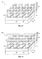
- FIGS. 1-8 are partial perspective views of a semiconductor device including a diode and a conductive strap during various processing acts in accordance with one embodiment of the disclosure
- FIGS. 9-14 are partial perspective views of a semiconductor device including a diode and a conductive strap during various processing acts in accordance with one embodiment of the disclosure.
- FIG. 15 is a schematic block diagram illustrating one embodiment of an electronic system that includes a semiconductor device including a diode and a conductive strap of the disclosure.
- the diode structure includes, for example, a conductive strap formed over an insulator material and a diode formed of a single crystalline silicon material formed over the conductive strap.
- the diode may be a vertical diode structure having a first doped region formed over the conductive strap and a second doped region formed over the first doped region.
- a memory cell may be formed over the diode.
- Methods of forming such structures include forming a base structure including a second semiconductor substrate having a first doped region and a second doped region, a conductive material, an adhesion material, and an insulator material over a first semiconductor substrate. A portion of the second semiconductor substrate, the conductive material, and the adhesion material may be removed to form the conductive strap and the diode structure.
- the diode structures formed in accordance with the various embodiments of the disclosure are formed of a single crystalline silicon material.
- conventional diodes are formed of a polysilicon material.
- Such conventional diodes exhibit poor I on /I off performance due to the low carrier mobility in the polysilicon material and current leaks, which typically form at the boundaries of the silicon grains.
- the I on /I off performance of the diode may be improved as the single crystalline silicon material has greater ion mobility than polysilicon material.
- current leaks are less likely to form within the single crystalline silicon material.
- the diodes formed from the single crystalline silicon material may be smaller than a diode formed of polysilicon material.
- the methods for forming the diode structures in accordance with various embodiments of the disclosure include forming a second semiconductor substrate overlying a conductive material. Because the conductive material, which may be used to form a conductive strap, is buried beneath the second semiconductor substrate, the diode structure may be formed in the second semiconductor substrate in relatively few process acts, as described in greater detail below. For example, in one embodiment, a cross point array including a plurality of diodes having a memory cell formed on each diode may be formed in as few as two patterning and etching acts.
- the diode structures are formed over the conductive strap, the diode structures may be self-aligned with the conductive strap and, thus, contact resistance caused by misalignment between the diode and the conductive strap may be reduced.
- the memory cell and the diode may also be self aligned, thus decreasing contact resistance caused by misalignment between the diode and the memory cell.
- the diode structures formed in accordance with various embodiments of the disclosure may be used to fabricate a variety of semiconductor devices, such as an integrated circuit including a logic device formed in/on the first semiconductor substrate and a memory device including the diode structure formed in/on the second semiconductor substrate. Since a logic device may be formed on the first semiconductor substrate before the memory device including the diode structure is formed, the memory device is not exposed to the processing conditions used for the formation of the logic device. By forming such vertical integrated circuits, the cell size may be reduced, which provides for increased cache memory density.
- the diode structures formed in accordance with various embodiments of the disclosure may be used to form, for example, flash memory, imagers, and phase change memory (PCRAM).
- PCRAM phase change memory
- the materials described herein may be formed by any suitable technique including, but not limited to, spin coating, blanket coating, chemical vapor deposition (“CVD”), plasma enhanced chemical vapor deposition (“PECVD”), atomic layer deposition (“ALD”), plasma enhanced ALD, or physical vapor deposition (“PVD”).
- CVD chemical vapor deposition
- PECVD plasma enhanced chemical vapor deposition
- ALD atomic layer deposition
- PVD physical vapor deposition
- materials may be grown in situ.
- a technique suitable for depositing or growing a particular material may be selected by a person of ordinary skill in the art. While the materials described and illustrated herein may be formed as layers, the materials are not limited thereto and may be formed in other three-dimensional configurations.
- FIGS. 1 through 8 are partial perspective views of a method of forming an embodiment of a semiconductor device 100 ( FIG. 8 ) of the present invention.
- the semiconductor device 100 may be formed using a semiconductor structure 34 ( FIG. 4 ), also referred to herein as a base structure 34 , which is formed by bonding an acceptor wafer 10 ( FIG. 1 ) and a donor wafer 16 ( FIG. 2 ). Forming such base structures 34 are described in detail in U.S. patent application Ser. No. 12/715,704 filed on Mar.
- FIGS. 1 through 4 illustrate one example of a method of forming the base structure 34
- any of the methods described in U.S. patent application Ser. No. 12/715,704, or other known methods, may be utilized to form the base structure 34 .
- FIG. 1 depicts the acceptor wafer 10 .
- the acceptor wafer 10 may include a first semiconductor substrate 12 having an insulator material 14 formed thereon.
- the first semiconductor substrate 12 may include a fabrication substrate, such as a full or partial wafer of semiconductor material (e.g., silicon, gallium arsenide, indium phosphide, etc.), a full or partial silicon-on-insulator (SOI) type substrate, such as a silicon-on-glass (SOG), silicon-on-ceramic (SOC), or silicon-on-sapphire (SOS) substrate, or any other known, suitable fabrication substrate.
- SOI silicon-on-insulator
- SOI silicon-on-insulator
- SOI silicon-on-insulator
- SOI silicon-on-insulator
- SOI silicon-on-insulator
- SOI silicon-on-insulator
- SOI silicon-on-insulator
- SOI silicon-on-insulator
- SOI silicon-on-insulator
- SOI silicon-
- the first semiconductor substrate 12 may be doped or undoped.
- An at least partially fabricated logic device such as a CMOS (complementary metal-oxide semiconductor) device, may optionally be present on the first semiconductor substrate 12 and may be formed by conventional techniques.
- the first semiconductor substrate 12 is bulk crystalline silicon.
- the insulator material 14 may be a dielectric material including, by way of non-limiting example, silicon dioxide, borophosphosilicate glass (BPSG), borosilicate glass (BSG), phosphosilicate glass (PSG), or the like. In one embodiment, the insulator material 14 is an oxide. The insulator material 14 may be from about 500 ⁇ thick to about 2 ⁇ m thick, such as from about 1000 ⁇ to about 2000 ⁇ . Techniques for deposition and in situ growth of such dielectric materials are known in the art and may include, for example, chemical vapor deposition (CVD), such as low pressure CVD or plasma enhanced CVD, atomic layer deposition (ALD), spin-on deposition, thermal decomposition, or thermal growth.
- CVD chemical vapor deposition
- ALD atomic layer deposition
- spin-on deposition thermal decomposition, or thermal growth.
- FIG. 2 is a partial perspective view of one embodiment of the donor wafer 16 used to form the base structure 34 ( FIG. 4 ).
- the donor wafer 16 may include a precursor semiconductor substrate 18 formed of a single crystalline silicon material.
- a conductive material 20 and an adhesion material 22 may be formed over the precursor semiconductor substrate 18 .
- the precursor semiconductor substrate 18 may, initially, be doped or undoped.
- the precursor semiconductor substrate 18 may initially be a single crystalline silicon material that is undoped or intrinsically doped.
- the precursor semiconductor substrate 18 may then be doped, or further doped, to include a first doped region 24 , a second doped region 26 , and a lightly doped region 28 . These doped regions may ultimately form the diode.
- the first doped region 24 and the second doped region 26 may be doped with P-type or N-type dopants such that the first doped region 24 and the second doped region 26 are oppositely doped.
- the first doped region 24 is an N-type single crystalline silicon material and the second doped region 26 is a P-type single crystalline silicon material.
- the first doped region 24 is a P-type single crystalline silicon material and the second doped region 26 is an N-type single crystalline silicon material.
- a lightly doped region 28 may be formed between the first doped region 24 and the second doped region 26 .
- the lightly doped region 28 may be doped with the same dopant as the second doped region 26 , but the lightly doped region 28 may have a lower concentration of dopant than the second doped region 26 .
- the second doped region 26 may be doped with a higher concentration of the P-type dopant and the lightly doped region 28 may be doped with a lower concentration of the P-type dopant.
- a Schottky diode may be formed at an interface between the first doped region 24 and the conductive material 20 , as known in the art.
- doped regions 24 , 26 , and 28 are described as being formed before the donor wafer 16 and acceptor wafer 10 are bonded, doping of the precursor semiconductor substrate 18 to form these regions may be conducted after the donor wafer 16 and the acceptor wafer 10 are bonded.
- the doped regions 24 , 26 , and 28 may be formed by a doping technique known in the art, such as diffusion or ion implantation techniques.
- a doping technique known in the art, such as diffusion or ion implantation techniques.
- the first doped region 24 may be formed by implanting ions of an N-type impurity, such as arsenic (As), phosphorous (P) or antimony (Sb), into the precursor semiconductor substrate 18 .
- an N-type impurity such as arsenic (As), phosphorous (P) or antimony (Sb)
- the second doped region 26 is a P-type single crystalline silicon material
- the second doped region 26 may be formed by implanting ions of a P-type impurity, such as boron (B), into the precursor semiconductor substrate 18 .
- the depth to which the ions are implanted into the precursor semiconductor substrate 18 is at least partially a function of the implant dose and energy.
- the depth of the implanted ions within the precursor semiconductor substrate 18 may correspond to a desired thickness of the first doped region 24 and the second doped region 26 .
- the first doped region 24 and the second doped region 26 may be formed before or after the conductive material 20 and the adhesion material 22 have been formed on the donor wafer 16 .
- the lightly doped region 28 may be doped using the same dopant as the second doped region 26 , except that a lower concentration of the dopant is implanted, such as by adjusting the implant dose or implant energy.
- the conductive material 20 may be a low resistivity conductive material including, but not limited to, a phase change material, titanium, titanium silicide, titanium oxide, titanium nitride, tantalum, tantalum silicide, tantalum oxide, tantalum nitride, tungsten, tungsten silicide, tungsten oxide, tungsten nitride, other metals, metal silicide, metal oxide, or metal nitride materials, or combinations thereof, including multiple, different conductive materials.
- the conductive material 20 is formed from titanium nitride because titanium nitride has good adherence or adhesion to many materials, such as the single crystalline silicon material used as the precursor semiconductor substrate 18 .
- Titanium nitride also has a high melting point (about 3000° C.), which makes it unaffected by high processing temperatures. Titanium nitride also makes excellent ohmic contact with other conductive materials. Titanium nitride is also commonly used in semiconductor fabrication and, therefore, may easily be incorporated into conventional fabrication processes.
- the conductive material 20 is a titanium-rich titanium nitride, such as metal mode titanium nitride (MMTiN).
- MMTiN metal mode titanium nitride
- the conductive material 20 may also be formed from multiple conductive materials. By way of non-limiting example, the conductive material 20 may be formed from a metal, such as titanium, tungsten or aluminum, with a layer of titanium material formed thereon.
- the thickness of the conductive material 20 may be optimized, depending on the material, to provide a low ohmic contact.
- the conductive material 20 is titanium nitride, such as MMTiN
- the conductive material 20 may have a thickness of from about 10 nm to about 50 nm.
- the conductive material 20 may be formed by a deposition technique known in the art, such as, for example, ALD, CVD, or PVD.
- the adhesion material 22 may include, for example, an amorphous material, such as an amorphous silicon material or an amorphous germanium material.
- the adhesion material 22 may be formed over the conductive material 20 by a deposition technique known in the art, such as, for example, ALD, CVD, or PVD. In one embodiment, the adhesion material 22 may be formed on the conductive material 20 by PVD, followed by chemical-mechanical planarization (CMP).
- CMP chemical-mechanical planarization
- the adhesion material 22 may be of sufficient thickness to adhere to the insulator material 14 of the acceptor wafer 10 as described in greater detail below. For example, the thickness of the adhesion material 22 may be from about 10 nm to about 50 nm.
- the donor wafer 16 may also include a cleave portion 30 formed by implanting an atomic species into the precursor semiconductor substrate 18 .
- the atomic species may be hydrogen ions, ions of rare gases, also termed inert or noble gases, or ions of fluorine.
- the atomic species may be implanted into the precursor semiconductor substrate 18 of the donor wafer 16 to form an implanted zone 32 .
- the atomic species may be implanted into the precursor semiconductor substrate 18 prior to formation of the conductive material 20 thereon, after formation of the conductive material 20 thereon, or after formation of the adhesion material 22 thereon.
- the implanted zone 32 may be formed at a desired depth in the precursor semiconductor substrate 18 , which is dependent on parameters such as implant dose and energy of the atomic species, as known in the art.
- the location of the implanted zone 32 may correspond to a height of a diode 48 ultimately formed from the precursor semiconductor substrate 18 , as shown in FIG. 7 .
- the implanted zone 32 may include microbubbles or microcavities including the implanted atomic species, which provide a weakened region within the precursor semiconductor substrate 18 .
- the donor wafer 16 may be thermally treated at a temperature above that at which implantation is effected, but below the melting temperature of the conductive material 20 , to effect crystalline rearrangement in the donor wafer 16 and coalescence of the microbubbles or microcavities.
- the donor wafer 16 may be cleaved at the implanted zone 32 , forming the second semiconductor substrate 18 ′ on the base structure 34 ( FIG. 4 ) and cleave portion 30 .
- the term “second semiconductor substrate” is used herein to refer to the semiconductor structure after removal of the cleave portion 30
- the term “precursor semiconductor substrate” is used herein to refer to the semiconductor structure before removal of the cleave portion 30 .
- the donor wafer 16 ( FIG. 2 ) may be superposed onto the acceptor wafer 10 ( FIG. 1 ) such that the adhesion material 22 of the donor wafer 16 is in contact with the insulator material 14 of the acceptor wafer 10 .
- the adhesion material 22 of the donor wafer 16 may then be bonded to the insulator material 14 of the acceptor wafer 10 by exposure to heat.
- at least one of the adhesion material 22 and the insulator material 14 may, optionally, be treated to improve the bond strength between the adhesion material 22 and the insulator material 14 .
- Such treatment techniques are known in the art and may include chemical, plasma, or implant activations.
- the insulator material 14 may be treated with a dilute ammonia hydroxide or hydrogen fluoride solution.
- the adhesion material 22 may also be exposed to a plasma of, for example, argon, to form a plasma-activated surface. Activating at least one of the adhesion material 22 and the insulator material 14 may increase the kinetics of the subsequent bonding therebetween
- the adhesion material 22 of the donor wafer 16 may be contacted and bonded with the insulator material 14 of the acceptor wafer 10 to form a precursor of the base structure 34 ( FIG. 4 ).
- the adhesion material 22 may be bonded to the insulator material 14 by, for example, heating the base structure 34 to a temperature of less than about 600° C., such as from about 300° C. to about 400° C. If the insulator material 14 is formed from silicon dioxide, silicon-oxide bonds may form between the adhesion material 22 and the insulator material 14 . Because the conductive material 20 may be formed of a metal or other heat sensitive material, the temperature to which the base structure 34 is exposed may be less than the melting point of the conductive material 20 .
- the adhesion material 22 and the insulator material 14 may also be bonded without heat, such as at ambient temperature (from about 20° C. to about 25° C.). Pressure may also be applied to the donor wafer 16 and the acceptor wafer 10 to bond the adhesion material 22 to the insulator material 14 . Once the donor wafer 16 is bonded to the acceptor wafer 10 , the conductive material 20 from the donor wafer 16 may form a buried conductive material, which is disposed between the insulator material 14 and the precursor semiconductor substrate 18 .
- the cleave portion 30 may then be removed from the precursor semiconductor substrate 18 to form the base structure 34 shown in FIG. 4 .
- the cleave portion 30 may be removed by techniques known in the art, such as by applying a shear force to the implanted zone 32 or by applying heat or a jet gas stream at the implanted zone 32 .
- the hydrogen or other ions implanted in implanted zone 32 produce a weakened region in the precursor semiconductor substrate 18 , which is susceptible to cleavage.
- the remaining portion of the precursor semiconductor substrate 18 (second semiconductor substrate 18 ′) may have a thickness, for example, of from about 50 nm to about 500 nm (from about 500 ⁇ to about 5000 ⁇ ).
- the second semiconductor substrate 18 ′ of the base structure 34 may be smoothed according to conventional techniques such as, for example, one or more of grinding, wet etching, and chemical-mechanical planarization (CMP).
- the base structure 34 may be formed by modification of SMART-CUT® layer transfer technology.
- the SMART-CUT® layer transfer technology is described in detail in, for example, U.S. Pat. No. RE 39,484 to Bruel, U.S. Pat. No. 6,303,468 to Aspar et al., U.S. Pat. No. 6,335,258 to Aspar et al., U.S. Pat. No. 6,756,286 to Moriceau et al., U.S. Pat. No. 6,809,044 to Aspar et al., U.S. Pat. No. 6,946,365 to Aspar et al., and U.S. Patent Application Publication No.
- a bottom electrode 36 , a memory medium 38 , and a top electrode 40 may be formed over the second semiconductor substrate 18 ′. If the second semiconductor substrate 18 ′ were not previously doped, as described above, the second semiconductor substrate 18 ′ may be doped prior to forming the bottom electrode 36 , the memory medium 38 , and the top electrode 40 .
- the bottom electrode 36 may be formed from a conductive material, such as titanium, titanium silicide, titanium nitride, tungsten, tungsten silicide, tungsten nitride, or combinations thereof.
- the bottom electrode 36 is MMTi, titanium, MMTi/titanium nitride, or titanium/titanium nitride.
- the bottom electrode 36 may be formed over the second semiconductor substrate 18 ′ using a deposition technique known in the art, such as, for example, ALD, CVD, or PVD.
- the memory medium 38 may be formed of any medium capable of holding distinct detectable states.
- the memory medium 38 may be formed of a transition metal material, such as nickel oxide or copper oxide, a phase change material, such as a chalcogenide material, or a resistive oxide material.
- the memory medium 38 includes a conductive oxide material, a solid electrolyte material, an antifuse oxide material, an ovonic material, or a ferroelectric material.
- the memory medium 38 may also be formed by a deposition technique known in the art, such as, ALD, CVD, or PVD.
- the top electrode 40 may be formed of a conductive material similar to the bottom electrode 36 .
- a two mask process may be used to define a cross point array including at least one diode 48 having a memory cell 46 thereon formed over a conductive strap 42 .
- the top electrode 40 , the memory medium 38 , the bottom electrode 36 , the second semiconductor substrate 18 ′, the conductive material 20 , and the adhesion 22 material may be patterned using a single mask to form pillars 45 having at least one first trench 44 there between. As shown in FIG.
- the top electrode 40 , the memory medium 38 , the bottom electrode 36 , the second semiconductor substrate 18 ′, the conductive material 20 , and the adhesion material 22 may be patterned and etched in a first direction Y, as described in greater detail below.
- the conductive material 20 underlying the pillars 45 forms the conductive strap 42 , which may also function as a word line in the semiconductor device 100 ( FIG. 8 ).
- the pillars 45 may be formed by depositing a mask material (not shown) over the top electrode 40 and patterning the mask material to form apertures through which surfaces of the top electrode 40 are exposed.
- the mask material may include, for example, a photoresist material, an oxide material, transparent carbon, or amorphous carbon. Methods of forming and patterning the mask material are known in the art and, therefore, are not described in detail herein.
- the pattern in the mask material may then be transferred to the underlying materials using dry or wet etch techniques.
- an anisotropic reactive ion (i.e., plasma) etching or reactive ion etching (RIE) process may be used.
- the etch technique may be selected by a person of ordinary skill in the art based on the material to be removed. Multiple materials may also be removed simultaneously, depending on the similarity in materials. The techniques for removing the underlying materials are conventional and, therefore, are not described in detail herein.
- the removed portions of the top electrode 40 , the memory medium 38 , the bottom electrode 36 , the second semiconductor substrate 18 ′, the conductive material 20 , and the adhesion material 22 may form the at least one first trench 44 .
- the portions of each of the top electrode 40 , the memory medium 38 , the bottom electrode 36 , the second semiconductor substrate 18 ′, the conductive material 20 , and the adhesion material 22 remaining under the mask material form the pillars 45 .
- the conductive material 20 at the bottom of the pillars 45 forms the conductive strap 42 .
- a portion of the insulator material 14 may also be etched in order to ensure complete electrical isolation of adjacent conductive straps 42 from one another.
- the remaining portions of the mask material overlying the pillars 45 may then be removed.
- the at least one first trench 44 may be formed extending in a first direction Y through each of the top electrode 40 , the memory medium 38 , the bottom electrode 36 , the second semiconductor substrate 18 ′, the conductive material 20 , and the adhesion material 22 .
- the top electrode 40 , the bottom electrode 36 , and the conductive material 20 are each formed from titanium nitride
- a mixture of bromine-containing gas and a fluorine-containing gas or a mixture of a fluorine-containing gas and a chlorine-containing gas may be used to remove each of these titanium nitride materials and the adhesion material 22 selective to the mask material and the insulator material 14 .
- the second semiconductor substrate 18 ′ may be selectively removed using a reactive ion etching (RIE) process using oxygen (O 2 ) gas and tetrafluoromethane (CF 4 ) gas.
- RIE reactive ion etching
- a fill material may be formed in the at least one first trench 44 and subject to CMP so that an upper surface 43 of the base structure 34 is substantially planar.
- the fill material may include, for example, a dielectric material such as an oxide material, a nitride material, or a spin-on-glass (SOG) material, and may be deposited using a chemical vapor deposition process.
- portions of the top electrode 40 , the memory medium 38 , the bottom electrode 36 , and the second semiconductor substrate 18 ′ may be patterned using a second mask to form at least one diode 48 having a memory cell 46 formed thereon.
- the diode 48 includes the first doped region 24 , the lightly doped region 28 , and the second doped region 26 .
- the memory cell 46 includes the bottom electrode 36 , the memory medium 38 , and the top electrode 40 .
- At least one second trench 47 may be formed between adjacent diodes 48 over a common conductive strap 42 .
- the lightly doped region 28 and a portion of the first doped region 24 may be patterned and etched in a second direction X to form at least one second trench 47 , as described in greater detail below.
- the second direction X may be substantially perpendicular to the first direction Y.
- the diode 48 is self-aligned with the conductive strap 42 thus eliminating the need for a separate electrical contact between the diode 48 and the conductive strap 42 .
- each diode 48 may be from about 2:1 to about 20:1 and, more particularly, from about 5:1 to about 10:1.
- the width of each diode 48 may be from about 5 nm to about 50 nm and, more particularly, from about 10 nm to about 20 nm. Because the diode 48 is formed of a single crystalline silicon material rather than a polysilicon material, the diode 48 may have a smaller width and height than a diode formed of polysilicon material.
- diodes formed of a polysilicon material have a lower carrier mobility than and experience a greater occurrence of leaks along the grain boundary, thus providing a lower performance than a diode formed of a single crystal silicon material. Additionally, because the diode 48 is formed of a single crystalline silicon material, the diode 48 may have a greater ability to transfer ions than a diode formed from polysilicon and, therefore, will have a greater I on /I off performance than a polysilicon diode.
- Each diode 48 and memory cell 46 may be formed by depositing a mask material (not shown) over the top electrode 40 and the fill material (not shown) and patterning the mask material to form apertures through which surfaces of the top electrode 40 are exposed.
- surfaces of the fill material (not shown) may also be exposed through the mask material.
- the mask material may include, for example, a photoresist material, an oxide material, transparent carbon or amorphous carbon. Methods of forming and patterning the mask material are known in the art and, therefore, are not described in detail herein.
- Portions of the top electrode 40 , the memory medium 38 , the bottom electrode 36 , and the second semiconductor substrate 18 ′ including the second doped region 26 , the partially doped region 28 , and a portion of the first doped region 24 that are exposed through the apertures in the mask material may be removed to form each diode 48 and memory cell 46 .
- the top electrode 40 and the bottom electrode 26 are each formed from titanium nitride
- a mixture of bromine-containing gas and a fluorine-containing gas or a mixture of a fluorine-containing gas and a chlorine-containing gas may be used to remove each of the titanium nitride materials selective to the mask material and the insulator material 14 .
- the second semiconductor substrate 18 ′ may be selectively removed using a reactive ion etching (RIE) process using oxygen (O 2 ) gas and tetrafluoromethane (CF 4 ) gas.
- RIE reactive ion etching
- An additional fill material may be formed in any etched portions of the at least one first trench 44 and the at least one second trench 47 and subject to CMP so that the upper surface 43 of the base structure 34 and the fill material are substantially planar with one another.
- a bottom electrode 52 may be formed over the second semiconductor substrate 18 ′. If the second semiconductor substrate 18 ′ was not previously doped, as described above, the second semiconductor substrate 18 ′ may be doped prior to forming the bottom electrode 52 .
- the bottom electrode 52 may be formed from a conductive material, such as titanium, titanium silicide, titanium nitride, tungsten, tungsten silicide, tungsten nitride, or combinations thereof.
- the bottom electrode 52 is MMTi, titanium, MMTi/titanium nitride, or titanium/titanium nitride.
- the bottom electrode 52 may be formed on the second semiconductor substrate 18 ′ using a deposition technique known in the art, such as, for example, ALD, CVD, or PVD.
- a two mask process may be used to define a cross point array including at least one diode 62 having a bottom electrode 52 thereon formed over a conductive strap 54 .
- the bottom electrode 52 , the second semiconductor substrate 18 ′, the conductive material 20 , and the adhesion material 22 may be removed using a first mask to form pillars 58 having trenches 56 there between.
- the bottom electrode 52 , the second semiconductor substrate 18 ′, the conductive material 20 , and the adhesion material 22 may be patterned and etched in a first direction Y as described in greater detail below.
- the conductive material 20 underlying the pillars 58 forms the conductive strap 54 , which may also function as a word line in the semiconductor device 200 ( FIG. 14 ).
- portions of the bottom electrode 52 and the second semiconductor substrate 18 ′ may be removed using a second mask to form at least one diode 62 having the bottom electrode 52 formed thereon.
- a trench 64 may be formed between adjacent diodes 62 over a common conductive strap 54 .
- the bottom electrode 52 and the second semiconductor substrate 18 ′ including the second doped region 26 the lightly doped region 28 and a portion of the first doped region 24 may be patterned and etched in a second direction X to form the trench 64 as described in greater detail below.
- the second direction X may be substantially perpendicular to the first direction Y.
- Each diode 62 may be formed by depositing a mask material (not shown) over the bottom electrode 52 and the fill material (not shown) and patterning the mask material to form apertures through which surfaces of the bottom electrode 52 are exposed.
- surfaces of the fill material (not shown) may also be exposed through the mask material.
- the mask material may include, for example, a photoresist material, an oxide material, transparent carbon or amorphous carbon. Methods of forming and patterning the mask material are known in the art and, therefore, are not described in detail herein.
- Portions of the bottom electrode 52 and the second semiconductor substrate 18 ′ including the second doped region 26 , the partially doped region 28 , and a portion of the first doped region 24 that are exposed through the apertures in the mask material may be removed to form each diode 62 having the bottom electrode 52 formed thereon.
- the bottom electrode 52 is formed from titanium nitride
- a mixture of bromine-containing gas and a fluorine-containing gas or a mixture of a fluorine-containing gas and a chlorine-containing gas may be used to selectively remove the titanium nitride materials selective to the mask material and the insulator material 14 .
- the second semiconductor substrate 18 ′ may be selectively removed using a reactive ion etching (RIE) process using oxygen (O 2 ) gas and tetrafluoromethane (CF 4 ) gas.
- RIE reactive ion etching
- An additional fill material may be formed in any etched portions of the trenches 56 and the trenches 64 and subject to CMP so that the upper surface 60 of the semiconductor structure and the fill material are substantially planar with one another.
- a memory medium 66 may be formed over the bottom electrode 52 .
- the memory medium 66 may be formed of any medium known in the art capable of holding a distinct detectable state or holding a charge.
- the memory medium 66 may be formed of a phase change or resistant material such as a chalcogenide material.
- Additional examples of the memory medium 66 include a conductive oxide material, a solid electrolyte material, an antifuse oxide material, an ovonic material, and a ferroelectric material.
- the memory medium 66 may be formed by a deposition technique known in the art, such as, for example ALD, CVD, or PVD. In one embodiment, the memory medium 66 may be blanket deposited over the upper surface 60 ( FIGS. 11 and 12 ) of the semiconductor structure. The memory medium 66 may then be patterned and etched as known in the art and as previously described herein such that the memory medium 66 is formed over each of the bottom electrodes 52 .
- At least one bit line 68 may be formed over the memory medium 66 .
- the bit line 68 may act as both a bit line and a top electrode.
- the bottom electrode 52 , the memory medium 66 , and the bit line 68 may form a memory cell 70 .
- the at least one bit line 68 may electrically couple more than one memory cell 70 .
- the bit line 68 may extend in the second direction X over adjacent memory cells 70 , electrically coupling memory cells 70 on two distinct conductive straps 54 .
- the bit line 68 may be formed by depositing a conductive material over the base structure 34 and patterning the conductive material to form substantially straight and substantially parallel bit lines 68 .
- a fill material (not shown) may be deposited in the trenches 56 and the trenches 64 as previously described and the bit line 68 may be blanket deposited over the pillars 58 and the fill material. The bit line 68 may then be patterned and etched, as known in the art, in the second direction X to expose the trenches 64 .
- the resulting semiconductor device 200 shown in FIG. 14 includes a cross-point diode memory array including the first semiconductor substrate 12 , the insulator material 14 , the adhesion material 22 bonded to the insulator material 14 , the conductive material 20 over the adhesion material 22 , wherein the conductive material 20 and the adhesion material 22 form at least two conductive straps 54 , a plurality of diodes 62 formed over the at least two conductive straps 54 , memory cells 70 formed on each of the plurality of diodes 62 , wherein the top electrode of the memory cell 70 is the bit line 68 .
- the semiconductor device 200 formed according to FIGS. 9-14 may be substantially similar to the semiconductor device 100 formed according to FIGS. 1-8 with the exception that in the semiconductor device 200 , the bit line 68 is the top electrode of the memory cell 70 while in the semiconductor device 100 , the bit line 50 is electrically coupled to the top electrode 40 of the memory cell 46 .
- FIG. 15 is a block diagram of an illustrative electronic system 300 according to the present invention.
- the electronic system 300 may include, for example, a computer or computer hardware component, a server or other networking hardware component, a cellular telephone, a digital camera, a personal digital assistant (PDA), portable media (e.g., music) player, etc.
- the electronic system 300 includes at least one memory device 301 .
- the electronic system 300 may further include at least one electronic signal processor device 302 (often referred to as a “microprocessor”).
- At least one of the electronic signal processor device 302 and the at least one memory device 301 may include, for example, an embodiment of the semiconductor device 100 , 200 described above.
- at least one of the electronic signal processor device 302 and the at least one memory device 301 may include an embodiment of a semiconductor device including a diode structure over a conductive material as previously described in relation to the semiconductor devices 100 , 200 shown in FIGS. 8 and 14 , respectively.
- the electronic system 300 may further include one or more input devices 304 for inputting information into the electronic system 300 by a user, such as, for example, a mouse or other pointing device, a keyboard, a touchpad, a button, or a control panel.
- the electronic system 300 may further include one or more output devices 306 for outputting information (e.g., visual or audio output) to a user such as, for example, a monitor, a display, a printer, an audio output jack, a speaker, etc.
- the input device 304 and the output device 306 may include a single touchscreen device that can be used both to input information to the electronic system 300 and to output visual information to a user.
- the one or more input devices 304 and output devices 306 may communicate electrically with at least one of the memory device 301 and the electronic signal processor device 302 .
- the present invention includes semiconductor devices including diode structures having a conductive strap and methods for forming such devices.
- Such devices may include a conductive material over an insulator material, at least one diode comprising a single crystalline silicon material over the conductive material, the diode having a first doped region overlying the conductive material and a second doped region overlying the first doped region wherein the conductivity of the first doped region is opposite the conductivity of the second doped region, and a memory cell over the second doped region.
- the memory cell may include a bottom electrode, a memory medium, and a top electrode.
- the top electrode may be a bit line. In other embodiments, a bit line may be electrically coupled to the memory cell.
- the present invention includes a semiconductor device that includes an insulator material on a first semiconductor substrate, an adhesion material bonded to the insulator material, a conductive material over the adhesion material, wherein the conductive material and the adhesion material are patterned to form at least one conductive strap, at least one diode over the conductive strap, and a memory cell on the at least one diode.
- the conductive strap may comprise a word line.
- the present invention includes a semiconductor device including a first semiconductor substrate having an insulator material thereon, an adhesion material bonded to the insulator material, a conductive material over the adhesion material, wherein the conductive material and the adhesion material are patterned to form at least two conductive straps, a plurality of diodes on each of the at least two conductive straps, each diode comprising a single crystalline silicon material, and a plurality of memory cells, one memory cell of the plurality of memory cells being on each of the plurality of diodes.
- the present invention includes methods for fabricating a semiconductor device that include forming a base comprising a second semiconductor substrate comprising a single crystalline silicon material having a first doped region and a second doped region, a conductive material, an adhesion material, and an insulator material overlying a first semiconductor substrate, forming a top electrode, a memory medium, and a bottom electrode over the second semiconductor substrate, removing a portion of the top electrode, the memory medium, the bottom electrode, the second semiconductor substrate, the conductive material, and the adhesion material to form at least one conductive strap having a pillar of the top electrode, the memory medium, the bottom electrode and the second semiconductor substrate thereon, and removing another portion of the top electrode, the memory medium, the bottom electrode, and the second semiconductor substrate to form at least one diode over the at least one conductive strap having a memory cell on the at least one diode.
- the present invention includes methods of forming a semiconductor device that include forming a base comprising a second semiconductor substrate comprising a single crystalline silicon material having a first doped region and a second doped region, a conductive material, an adhesion material, and an insulator material overlying a first semiconductor substrate, forming a bottom electrode over the second semiconductor substrate, removing a portion of the bottom electrode, the second semiconductor substrate, the conductive material, and the adhesion material to form at least one conductive strap having a pillar of the bottom electrode and the second semiconductor substrate thereon, and removing another portion of the bottom electrode, and the second semiconductor substrate to form at least one diode over the at least one conductive strap having a portion of the bottom electrode on the at least one diode, forming a memory medium over each portion of the bottom electrode, and forming at bit line over the memory medium.
Abstract
Description
Claims (14)
Priority Applications (5)
| Application Number | Priority Date | Filing Date | Title |
|---|---|---|---|
| US12/715,704 US9608119B2 (en) | 2010-03-02 | 2010-03-02 | Semiconductor-metal-on-insulator structures, methods of forming such structures, and semiconductor devices including such structures |
| US13/965,463 US8980699B2 (en) | 2010-03-02 | 2013-08-13 | Thyristor-based memory cells, devices and systems including the same and methods for forming the same |
| US14/642,866 US9343462B2 (en) | 2010-03-02 | 2015-03-10 | Thyristor-based memory cells, devices and systems including the same and methods for forming the same |
| US15/464,060 US10325926B2 (en) | 2010-03-02 | 2017-03-20 | Semiconductor-metal-on-insulator structures, methods of forming such structures, and semiconductor devices including such structures |
| US15/481,301 US10157769B2 (en) | 2010-03-02 | 2017-04-06 | Semiconductor devices including a diode structure over a conductive strap and methods of forming such semiconductor devices |
Applications Claiming Priority (4)
| Application Number | Priority Date | Filing Date | Title |
|---|---|---|---|
| US12/715,704 US9608119B2 (en) | 2010-03-02 | 2010-03-02 | Semiconductor-metal-on-insulator structures, methods of forming such structures, and semiconductor devices including such structures |
| US12/715,922 US8507966B2 (en) | 2010-03-02 | 2010-03-02 | Semiconductor cells, arrays, devices and systems having a buried conductive line and methods for forming the same |
| US12/715,889 US8288795B2 (en) | 2010-03-02 | 2010-03-02 | Thyristor based memory cells, devices and systems including the same and methods for forming the same |
| US12/715,843 US8513722B2 (en) | 2010-03-02 | 2010-03-02 | Floating body cell structures, devices including same, and methods for forming same |
Related Child Applications (1)
| Application Number | Title | Priority Date | Filing Date |
|---|---|---|---|
| US15/481,301 Division US10157769B2 (en) | 2010-03-02 | 2017-04-06 | Semiconductor devices including a diode structure over a conductive strap and methods of forming such semiconductor devices |
Publications (2)
| Publication Number | Publication Date |
|---|---|
| US20110215436A1 US20110215436A1 (en) | 2011-09-08 |
| US9646869B2 true US9646869B2 (en) | 2017-05-09 |
Family
ID=58670315
Family Applications (1)
| Application Number | Title | Priority Date | Filing Date |
|---|---|---|---|
| US12/715,743 Active 2030-10-14 US9646869B2 (en) | 2010-03-02 | 2010-03-02 | Semiconductor devices including a diode structure over a conductive strap and methods of forming such semiconductor devices |
Country Status (1)
| Country | Link |
|---|---|
| US (1) | US9646869B2 (en) |
Cited By (5)
| Publication number | Priority date | Publication date | Assignee | Title |
|---|---|---|---|---|
| US10923593B1 (en) * | 2019-08-09 | 2021-02-16 | Micron Technology, Inc. | Transistor and methods of forming transistors |
| US10964811B2 (en) | 2019-08-09 | 2021-03-30 | Micron Technology, Inc. | Transistor and methods of forming transistors |
| US11024736B2 (en) | 2019-08-09 | 2021-06-01 | Micron Technology, Inc. | Transistor and methods of forming integrated circuitry |
| US11417730B2 (en) | 2019-08-09 | 2022-08-16 | Micron Technology, Inc. | Vertical transistors with channel region having vertically elongated crystal grains that individually are directly against both of the top and bottom source/drain regions |
| US11637175B2 (en) | 2020-12-09 | 2023-04-25 | Micron Technology, Inc. | Vertical transistors |
Families Citing this family (28)
| Publication number | Priority date | Publication date | Assignee | Title |
|---|---|---|---|---|
| US8288795B2 (en) | 2010-03-02 | 2012-10-16 | Micron Technology, Inc. | Thyristor based memory cells, devices and systems including the same and methods for forming the same |
| US9646869B2 (en) | 2010-03-02 | 2017-05-09 | Micron Technology, Inc. | Semiconductor devices including a diode structure over a conductive strap and methods of forming such semiconductor devices |
| US9608119B2 (en) | 2010-03-02 | 2017-03-28 | Micron Technology, Inc. | Semiconductor-metal-on-insulator structures, methods of forming such structures, and semiconductor devices including such structures |
| US8513722B2 (en) | 2010-03-02 | 2013-08-20 | Micron Technology, Inc. | Floating body cell structures, devices including same, and methods for forming same |
| US8507966B2 (en) | 2010-03-02 | 2013-08-13 | Micron Technology, Inc. | Semiconductor cells, arrays, devices and systems having a buried conductive line and methods for forming the same |
| US8598621B2 (en) | 2011-02-11 | 2013-12-03 | Micron Technology, Inc. | Memory cells, memory arrays, methods of forming memory cells, and methods of forming a shared doped semiconductor region of a vertically oriented thyristor and a vertically oriented access transistor |
| US8952418B2 (en) | 2011-03-01 | 2015-02-10 | Micron Technology, Inc. | Gated bipolar junction transistors |
| US8519431B2 (en) | 2011-03-08 | 2013-08-27 | Micron Technology, Inc. | Thyristors |
| US8486743B2 (en) | 2011-03-23 | 2013-07-16 | Micron Technology, Inc. | Methods of forming memory cells |
| US8772848B2 (en) | 2011-07-26 | 2014-07-08 | Micron Technology, Inc. | Circuit structures, memory circuitry, and methods |
| US8994489B2 (en) | 2011-10-19 | 2015-03-31 | Micron Technology, Inc. | Fuses, and methods of forming and using fuses |
| US9252188B2 (en) * | 2011-11-17 | 2016-02-02 | Micron Technology, Inc. | Methods of forming memory cells |
| US8723155B2 (en) | 2011-11-17 | 2014-05-13 | Micron Technology, Inc. | Memory cells and integrated devices |
| US8546231B2 (en) | 2011-11-17 | 2013-10-01 | Micron Technology, Inc. | Memory arrays and methods of forming memory cells |
| US8728940B2 (en) | 2012-01-26 | 2014-05-20 | Micron Technology, Inc. | Memory arrays and methods of forming same |
| US9136467B2 (en) | 2012-04-30 | 2015-09-15 | Micron Technology, Inc. | Phase change memory cells and methods of forming phase change memory cells |
| US8765555B2 (en) | 2012-04-30 | 2014-07-01 | Micron Technology, Inc. | Phase change memory cells and methods of forming phase change memory cells |
| US8885382B2 (en) | 2012-06-29 | 2014-11-11 | Intel Corporation | Compact socket connection to cross-point array |
| US9680094B2 (en) * | 2012-08-30 | 2017-06-13 | Kabushiki Kaisha Toshiba | Memory device and method for manufacturing the same |
| US9553262B2 (en) | 2013-02-07 | 2017-01-24 | Micron Technology, Inc. | Arrays of memory cells and methods of forming an array of memory cells |
| US9608204B2 (en) * | 2013-09-09 | 2017-03-28 | Taiwan Semiconductor Manufacturing Company Ltd. | Resistive random access memory and manufacturing method thereof |
| US9443763B2 (en) * | 2013-09-12 | 2016-09-13 | Micron Technology, Inc. | Methods for forming interconnections between top electrodes in memory cells by a two-step chemical-mechanical polishing (CMP) process |
| US9257431B2 (en) | 2013-09-25 | 2016-02-09 | Micron Technology, Inc. | Memory cell with independently-sized electrode |
| US9881971B2 (en) | 2014-04-01 | 2018-01-30 | Micron Technology, Inc. | Memory arrays |
| US9362494B2 (en) | 2014-06-02 | 2016-06-07 | Micron Technology, Inc. | Array of cross point memory cells and methods of forming an array of cross point memory cells |
| US9343506B2 (en) | 2014-06-04 | 2016-05-17 | Micron Technology, Inc. | Memory arrays with polygonal memory cells having specific sidewall orientations |
| US10043808B1 (en) * | 2017-03-16 | 2018-08-07 | Toshiba Memory Corporation | Semiconductor memory |
| US10497712B2 (en) * | 2017-03-16 | 2019-12-03 | Toshiba Memory Corporation | Semiconductor memory |
Citations (247)
| Publication number | Priority date | Publication date | Assignee | Title |
|---|---|---|---|---|
| US3988771A (en) | 1974-05-28 | 1976-10-26 | General Electric Company | Spatial control of lifetime in semiconductor device |
| US4487639A (en) | 1980-09-26 | 1984-12-11 | Texas Instruments Incorporated | Localized epitaxy for VLSI devices |
| JPH02275663A (en) | 1989-01-24 | 1990-11-09 | Fujitsu Ltd | Semiconductor device and manufacture thereof |
| JPH0464249A (en) | 1990-07-04 | 1992-02-28 | Fujitsu Ltd | Manufacture of soi substrate |
| US5098861A (en) | 1991-01-08 | 1992-03-24 | Unitrode Corporation | Method of processing a semiconductor substrate including silicide bonding |
| US5102821A (en) | 1990-12-20 | 1992-04-07 | Texas Instruments Incorporated | SOI/semiconductor heterostructure fabrication by wafer bonding of polysilicon to titanium |
| US5106776A (en) | 1988-06-01 | 1992-04-21 | Texas Instruments Incorporated | Method of making high performance composed pillar dRAM cell |
| JPH04186815A (en) | 1990-11-21 | 1992-07-03 | Fujitsu Ltd | Manufacture of silicon-on-insulator substrate |
| JPH04283914A (en) | 1991-03-12 | 1992-10-08 | Fujitsu Ltd | Cladded semiconductor substrate and production method thereof |
| US5260233A (en) | 1992-11-06 | 1993-11-09 | International Business Machines Corporation | Semiconductor device and wafer structure having a planar buried interconnect by wafer bonding |
| JPH06104446A (en) | 1992-09-22 | 1994-04-15 | Toshiba Corp | Semiconductor device |
| US5378316A (en) | 1991-04-03 | 1995-01-03 | Eastman Kodak Company | High durability mask for dry etch processing of GaAs |
| US5412598A (en) | 1992-04-27 | 1995-05-02 | The University Of British Columbia | Bistable four layer device, memory cell, and method for storing and retrieving binary information |
| US5465249A (en) | 1991-11-26 | 1995-11-07 | Cree Research, Inc. | Nonvolatile random access memory device having transistor and capacitor made in silicon carbide substrate |
| US5471039A (en) | 1994-06-22 | 1995-11-28 | Panda Eng. Inc. | Electronic validation machine for documents |
| JPH0888153A (en) | 1994-09-19 | 1996-04-02 | Toshiba Corp | Laminated structure wafer and formation thereof |
| US5510630A (en) | 1993-10-18 | 1996-04-23 | Westinghouse Electric Corporation | Non-volatile random access memory cell constructed of silicon carbide |
| US5563084A (en) | 1994-09-22 | 1996-10-08 | Fraunhofer-Gesellschaft zur F orderung der angewandten Forschung e.V. | Method of making a three-dimensional integrated circuit |
| US5600160A (en) | 1993-04-14 | 1997-02-04 | Hvistendahl; Douglas D. | Multichannel field effect device |
| JPH10150176A (en) | 1996-11-15 | 1998-06-02 | Tadahiro Omi | Semiconductor substrate and its manufacture |
| US5874760A (en) | 1997-01-22 | 1999-02-23 | International Business Machines Corporation | 4F-square memory cell having vertical floating-gate transistors with self-aligned shallow trench isolation |
| JPH11103035A (en) | 1997-07-30 | 1999-04-13 | Tadahiro Omi | Semiconductor substrate and manufacture thereof |
| US5904507A (en) * | 1998-02-23 | 1999-05-18 | National Semiconductor Corporation | Programmable anti-fuses using laser writing |
| US5909618A (en) | 1997-07-08 | 1999-06-01 | Micron Technology, Inc. | Method of making memory cell with vertical transistor and buried word and body lines |
| US5920105A (en) | 1996-09-19 | 1999-07-06 | Fujitsu Limited | Compound semiconductor field effect transistor having an amorphous gas gate insulation layer |
| US5930640A (en) | 1995-06-07 | 1999-07-27 | International Business Machines Corporation | Mechanical supports for very thin stacked capacitor plates |
| US5936274A (en) | 1997-07-08 | 1999-08-10 | Micron Technology, Inc. | High density flash memory |
| US5963469A (en) | 1998-02-24 | 1999-10-05 | Micron Technology, Inc. | Vertical bipolar read access for low voltage memory cell |
| US6017778A (en) | 1994-12-30 | 2000-01-25 | Sgs-Thomson Microelectronics S.A. | Method for making power integrated circuit |
| JP2000150905A (en) | 1998-09-04 | 2000-05-30 | Semiconductor Energy Lab Co Ltd | Manufacture of semiconductor device |
| US6137128A (en) | 1998-06-09 | 2000-10-24 | International Business Machines Corporation | Self-isolated and self-aligned 4F-square vertical fet-trench dram cells |
| US6191476B1 (en) | 1992-10-21 | 2001-02-20 | Seiko Instruments Inc. | Semiconductor device |
| US6225151B1 (en) | 1997-06-09 | 2001-05-01 | Advanced Micro Devices, Inc. | Nitrogen liner beneath transistor source/drain regions to retard dopant diffusion |
| US6225165B1 (en) | 1998-05-13 | 2001-05-01 | Micron Technology, Inc. | High density SRAM cell with latched vertical transistors |
| US6229161B1 (en) | 1998-06-05 | 2001-05-08 | Stanford University | Semiconductor capacitively-coupled NDR device and its applications in high-density high-speed memories and in power switches |
| US6245663B1 (en) | 1998-09-30 | 2001-06-12 | Conexant Systems, Inc. | IC interconnect structures and methods for making same |
| US6255731B1 (en) | 1997-07-30 | 2001-07-03 | Canon Kabushiki Kaisha | SOI bonding structure |
| US6274888B1 (en) | 1999-01-11 | 2001-08-14 | Hitachi, Ltd | Semiconductor device including a TFT having large-grain polycrystalline active layer, LCD employing the same and method of fabricating them |
| US6294418B1 (en) | 1998-02-24 | 2001-09-25 | Micron Technology, Inc. | Circuits and methods using vertical complementary transistors |
| US20010024841A1 (en) | 1998-05-13 | 2001-09-27 | Noble Wendell P. | High density vertical sram cell using bipolar latchup induced by gated diode breakdown |
| US20010026477A1 (en) | 1999-01-19 | 2001-10-04 | Micron Technology, Inc. | Integrated circuit having an on-board reference generator |
| US6303468B1 (en) | 1997-08-12 | 2001-10-16 | Commissariat A L'energie Atomique | Method for making a thin film of solid material |
| US20010048119A1 (en) | 2000-03-17 | 2001-12-06 | Kabushiki Kaisha Toshiba | Semiconductor device and method of manufacturing the same |
| US6335258B1 (en) | 1996-11-05 | 2002-01-01 | Commissariat A L'energie Atomique | Method for making a thin film on a support and resulting structure including an additional thinning stage before heat treatment causes micro-cavities to separate substrate element |
| US20020024152A1 (en) | 2000-07-10 | 2002-02-28 | Kazutaka Momoi | Semiconductor member, semiconductor device and manufacturing methods thereof |
| US6352894B1 (en) | 1998-03-23 | 2002-03-05 | Siemens Aktiengesellschaft | Method of forming DRAM cell arrangement |
| US20020028541A1 (en) | 2000-08-14 | 2002-03-07 | Lee Thomas H. | Dense arrays and charge storage devices, and methods for making same |
| US6355501B1 (en) | 2000-09-21 | 2002-03-12 | International Business Machines Corporation | Three-dimensional chip stacking assembly |
| US6355520B1 (en) | 1999-08-16 | 2002-03-12 | Infineon Technologies Ag | Method for fabricating 4F2 memory cells with improved gate conductor structure |
| US6365488B1 (en) | 1998-03-05 | 2002-04-02 | Industrial Technology Research Institute | Method of manufacturing SOI wafer with buried layer |
| US6391658B1 (en) | 1999-10-26 | 2002-05-21 | International Business Machines Corporation | Formation of arrays of microelectronic elements |
| US20020070454A1 (en) | 2000-11-30 | 2002-06-13 | Seiko Epson Corporation | SOI substrate, element substrate, semiconductor device, electro-optical apparatus, electronic equipment, method of manufacturing the SOI substrate, method of manufacturing the element substrate, and method of manufacturing the electro-optical apparatus |
| US20020079537A1 (en) | 2000-12-20 | 2002-06-27 | Houston Theodore W. | Semiconductor on insulator device architecture and method of construction |
| US20020094619A1 (en) | 2001-01-18 | 2002-07-18 | International Business Machines Corportion | 6F2 Trench edram cell with double-gated vertical MOSFET and self-aligned STI |
| US20020142562A1 (en) | 2000-05-08 | 2002-10-03 | Chan Kevin K. | Method for manufacturing device substrate with metal back-gate and structure formed thereby |
| US20020158254A1 (en) | 2001-04-30 | 2002-10-31 | International Business Machines Corporation | Memory system capable of operating at high temperatures and method for fabricating the same |
| US20020163019A1 (en) * | 1990-10-15 | 2002-11-07 | Mohsen Amr M. | Interconnect substrate with circuits for field-programmability and testing of multichip modules and hybrid circuits |
| US6492662B2 (en) | 2001-04-16 | 2002-12-10 | Ibm Corporation | T-RAM structure having dual vertical devices and method for fabricating the same |
| US20020185684A1 (en) | 2001-06-12 | 2002-12-12 | International Business Machines Corporation | Method and structure for buried circuits and devices |
| US20020190265A1 (en) | 2001-06-13 | 2002-12-19 | International Business Machines Corporation | T-Ram cell having a buried vertical thyristor and a pseudo-TFT transfer gate and method for fabricating the same |
| US20020190298A1 (en) | 2001-06-13 | 2002-12-19 | Johann Alsmeier | Trench capacitor of a dram memory cell with a metallic collar region and a non-metallic buried strap to a selection transistor |
| US20030006461A1 (en) | 2001-07-06 | 2003-01-09 | Kabushiki Kaisha Toshiba | Integrated circuit device |
| JP2003030980A (en) | 2001-07-13 | 2003-01-31 | Toshiba Corp | Semiconductor memory |
| US6525953B1 (en) * | 2001-08-13 | 2003-02-25 | Matrix Semiconductor, Inc. | Vertically-stacked, field-programmable, nonvolatile memory and method of fabrication |
| US20030102469A1 (en) | 2001-11-30 | 2003-06-05 | Jones Robert E. | Semiconductor device and method therefor |
| US6576944B2 (en) | 2000-12-14 | 2003-06-10 | Infineon Technologies Ag | Self-aligned nitride pattern for improved process window |
| US6593624B2 (en) | 2001-09-25 | 2003-07-15 | Matrix Semiconductor, Inc. | Thin film transistors with vertically offset drain regions |
| US6600173B2 (en) | 2000-08-30 | 2003-07-29 | Cornell Research Foundation, Inc. | Low temperature semiconductor layering and three-dimensional electronic circuits using the layering |
| US20030211705A1 (en) | 2000-02-16 | 2003-11-13 | Ziptronix, Inc. | Method for low temperature bonding and bonded structure |
| US6649980B2 (en) | 2000-12-11 | 2003-11-18 | Sony Corporation | Semiconductor device with MOS transistors sharing electrode |
| US20030223292A1 (en) | 2002-05-16 | 2003-12-04 | Hasan Nejad | Stacked 1T-nmemory cell structure |
| US20030235710A1 (en) * | 2002-06-19 | 2003-12-25 | International Business Machines Corporation | Structures with improved adhesion to Si and C containing dielectrics and method for preparing the same |
| US20040007717A1 (en) | 2002-07-10 | 2004-01-15 | Yoo In-Kyeong | Memory device having a transistor and one resistant element as a storing means and method for driving the memory device |
| US20040022105A1 (en) | 2000-08-17 | 2004-02-05 | Kabushiki Kaisha Toshiba | Semiconductor memory device and method of manufacturing the same |
| US6690039B1 (en) | 2002-10-01 | 2004-02-10 | T-Ram, Inc. | Thyristor-based device that inhibits undesirable conductive channel formation |
| US6713791B2 (en) | 2001-01-26 | 2004-03-30 | Ibm Corporation | T-RAM array having a planar cell structure and method for fabricating the same |
| US6713810B1 (en) | 2003-02-10 | 2004-03-30 | Micron Technology, Inc. | Non-volatile devices, and electronic systems comprising non-volatile devices |
| US20040097022A1 (en) | 2002-05-07 | 2004-05-20 | Werkhoven Christiaan J. | Silicon-on-insulator structures and methods |
| US20040094758A1 (en) | 2002-07-29 | 2004-05-20 | Koji Usuda | Semiconductor apparatus |
| US6744094B2 (en) | 2001-08-24 | 2004-06-01 | Micron Technology Inc. | Floating gate transistor with horizontal gate layers stacked next to vertical body |
| US6756286B1 (en) | 1997-12-30 | 2004-06-29 | Commissariat A L'energie Atomique | Method for transferring a thin film comprising a step of generating inclusions |
| US20040130015A1 (en) * | 2002-12-25 | 2004-07-08 | Mitsuhiko Ogihara | Semiconductor apparatus having adhesion layer and semiconductor thin film |
| US6768156B1 (en) * | 2003-02-10 | 2004-07-27 | Micron Technology, Inc. | Non-volatile random access memory cells associated with thin film constructions |
| US20040174734A1 (en) | 2003-03-04 | 2004-09-09 | Micron Technology, Inc. | Vertical gain cell |
| US6809044B1 (en) | 1999-06-30 | 2004-10-26 | Commissariat A L'energie Atomique | Method for making a thin film using pressurization |
| JP2004303398A (en) | 2003-03-20 | 2004-10-28 | Matsushita Electric Ind Co Ltd | Head support device and disk device using the same |
| US6812504B2 (en) | 2003-02-10 | 2004-11-02 | Micron Technology, Inc. | TFT-based random access memory cells comprising thyristors |
| US6815781B2 (en) | 2001-09-25 | 2004-11-09 | Matrix Semiconductor, Inc. | Inverted staggered thin film transistor with salicided source/drain structures and method of making same |
| US20040233761A1 (en) * | 1998-10-30 | 2004-11-25 | Schwabe Nikolai Franz Gregoe | Magnetic storage device |
| US20040262679A1 (en) | 2003-06-30 | 2004-12-30 | Kabushiki Kaisha Toshiba | Semiconductor storage device and semiconductor integrated circuit |
| US20040262635A1 (en) | 2003-06-24 | 2004-12-30 | Sang-Yun Lee | Three-dimensional integrated circuit structure and method of making same |
| US20050001232A1 (en) | 2003-07-02 | 2005-01-06 | Micron Technology, Inc. | High-performance one-transistor memory cell |
| US6841813B2 (en) | 2001-08-13 | 2005-01-11 | Matrix Semiconductor, Inc. | TFT mask ROM and method for making same |
| US6845034B2 (en) | 2003-03-11 | 2005-01-18 | Micron Technology, Inc. | Electronic systems, constructions for detecting properties of objects, and assemblies for identifying persons |
| US20050037582A1 (en) | 2003-08-13 | 2005-02-17 | International Business Machines Corporation | Device threshold control of front-gate silicon-on-insulator mosfet using a self-aligned back-gate |
| US20050059252A1 (en) | 2003-09-15 | 2005-03-17 | International Business Machines Corporation | Self-aligned planar double-gate process by self-aligned oxidation |
| US6870202B2 (en) | 2001-11-07 | 2005-03-22 | Shindengen Electric Manufacturing Co., Ltd. | Surge protection semiconductor device |
| US20050062079A1 (en) * | 2003-09-18 | 2005-03-24 | Chao-I Wu | [methods for forming pn junction, one-time programmable read-only memory and fabricating processes thereof] |
| US6882008B1 (en) | 2003-10-30 | 2005-04-19 | Kabushiki Kaisha Toshiba | Semiconductor integrated circuit device |
| US6888199B2 (en) | 2003-10-07 | 2005-05-03 | International Business Machines Corporation | High-density split-gate FinFET |
| US6891205B1 (en) | 2001-03-22 | 2005-05-10 | T-Ram, Inc. | Stability in thyristor-based memory device |
| US6914286B2 (en) | 2002-06-27 | 2005-07-05 | Samsung Electronics Co., Ltd. | Semiconductor memory devices using sidewall spacers |
| US20050146955A1 (en) * | 2003-11-11 | 2005-07-07 | Takeshi Kajiyama | Resistance change memory having organic semiconductor layer |
| US6934209B2 (en) | 2002-06-06 | 2005-08-23 | Micron Technology, Inc. | Temperature compensated T-RAM memory device and method |
| US6940761B2 (en) | 2002-08-29 | 2005-09-06 | Micron Technology, Inc. | Merged MOS-bipolar capacitor memory cell |
| US6940748B2 (en) | 2002-05-16 | 2005-09-06 | Micron Technology, Inc. | Stacked 1T-nMTJ MRAM structure |
| US6946365B2 (en) | 2000-12-08 | 2005-09-20 | Commissariat A L'energie Atomique | Method for producing a thin film comprising introduction of gaseous species |
| US6953953B1 (en) | 2002-10-01 | 2005-10-11 | T-Ram, Inc. | Deep trench isolation for thyristor-based semiconductor device |
| US20050230356A1 (en) * | 2002-04-02 | 2005-10-20 | Nanosys, Inc. | Methods of making, positioning and orienting nanostructures, nanostructure arrays and nanostructure devices |
| US6958513B2 (en) | 2003-06-06 | 2005-10-25 | Chih-Hsin Wang | Floating-gate memory cell having trench structure with ballistic-charge injector, and the array of memory cells |
| US6965129B1 (en) | 2002-11-06 | 2005-11-15 | T-Ram, Inc. | Thyristor-based device having dual control ports |
| JP2005327766A (en) | 2004-05-12 | 2005-11-24 | Fujitsu Ltd | System lsi using fin-type channel fet and method for manufacture same |
| US20050282356A1 (en) | 2004-06-21 | 2005-12-22 | Sang-Yun Lee | Semiconductor layer structure and method of making the same |
| US20050282318A1 (en) | 2004-06-18 | 2005-12-22 | Dao Thuy B | Method of forming a transistor with a bottom gate |
| US20060010056A1 (en) | 2004-02-12 | 2006-01-12 | De La Motte Alain L | System and method for high-yield returns in riskless-principal interest rate/yield arbitrage |
| US6995456B2 (en) | 2004-03-12 | 2006-02-07 | International Business Machines Corporation | High-performance CMOS SOI devices on hybrid crystal-oriented substrates |
| US20060034116A1 (en) * | 2004-08-13 | 2006-02-16 | Lam Chung H | Cross point array cell with series connected semiconductor diode and phase change storage media |
| US7015092B2 (en) | 2003-12-18 | 2006-03-21 | Infineon Technologies North America Corp. | Methods for forming vertical gate transistors providing improved isolation and alignment of vertical gate contacts |
| US20060071074A1 (en) | 2004-09-29 | 2006-04-06 | Matrix Semiconductor, Inc. | Doped polysilicon via connecting polysilicon layers |
| US20060082004A1 (en) | 2003-07-07 | 2006-04-20 | Parekh Kunal R | Methods of forming memory circuitry |
| US20060099776A1 (en) | 2004-11-09 | 2006-05-11 | Frederic Dupont | Methods for fabricating compound material wafers |
| US20060124974A1 (en) | 2004-12-15 | 2006-06-15 | International Business Machines Corporation | Structure and method to generate local mechanical gate stress for mosfet channel mobility modification |
| US20060125011A1 (en) | 2004-03-31 | 2006-06-15 | Chang Peter L | Memory with split gate devices and method of fabrication |
| US7075146B2 (en) | 2004-02-24 | 2006-07-11 | Micron Technology, Inc. | 4F2 EEPROM NROM memory arrays with vertical devices |
| US7081663B2 (en) | 2002-01-18 | 2006-07-25 | National Semiconductor Corporation | Gate-enhanced junction varactor with gradual capacitance variation |
| US20060197115A1 (en) * | 2003-04-03 | 2006-09-07 | Haruki Toda | Phase change memory device |
| US7120046B1 (en) | 2005-05-13 | 2006-10-10 | Micron Technology, Inc. | Memory array with surrounding gate access transistors and capacitors with global and staggered local bit lines |
| US20060227601A1 (en) | 2004-08-24 | 2006-10-12 | Micron Technology, Inc. | Memory cell with trenched gated thyristor |
| US20060249770A1 (en) | 2005-05-03 | 2006-11-09 | Samsung Electronics Co., Ltd. | Single Transistor Floating-Body DRAM Devices Having Vertical Channel Transistor Structures and Methods of Fabricating the Same |
| US7151024B1 (en) | 2004-09-02 | 2006-12-19 | Micron Technology, Inc. | Long retention time single transistor vertical memory gain cell |
| KR100663359B1 (en) | 2005-03-31 | 2007-01-02 | 삼성전자주식회사 | One transistor floating body DRAM cell with recess channel transistor structure and method of fabricating the same |
| US7157771B2 (en) | 2004-01-30 | 2007-01-02 | Micron Technology, Inc. | Vertical device 4F2 EEPROM memory |
| US20070012945A1 (en) | 2005-07-15 | 2007-01-18 | Sony Corporation | Semiconductor device and method for manufacturing semiconductor device |
| US20070018166A1 (en) | 2005-07-22 | 2007-01-25 | Atanackovic Petar B | Stacked transistors and process |
| US20070018223A1 (en) | 2005-07-25 | 2007-01-25 | Micron Technology Inc. | Dram including a vertical surround gate transistor |
| US20070023805A1 (en) | 2005-07-26 | 2007-02-01 | Wells David H | Reverse construction memory cell |
| USRE39484E1 (en) | 1991-09-18 | 2007-02-06 | Commissariat A L'energie Atomique | Process for the production of thin semiconductor material films |
| US7180135B1 (en) | 2003-10-06 | 2007-02-20 | George Mason Intellectual Properties, Inc. | Double gate (DG) SOI ratioed logic with intrinsically on symmetric DG-MOSFET load |
| US20070045709A1 (en) | 2005-08-29 | 2007-03-01 | Taiwan Semiconductor Manufacturing Co., Ltd. | Vertical flash memory |
| US20070047364A1 (en) | 2005-08-31 | 2007-03-01 | International Business Machines Corporation | Methods and apparatus for varying a supply voltage or reference voltage using independent control of diode voltage in asymmetrical double-gate devices |
| US20070057328A1 (en) | 1999-05-18 | 2007-03-15 | Fujitsu Limited | Semiconductor device and its manufacture |
| US20070064342A1 (en) | 2005-09-20 | 2007-03-22 | Kabushiki Kaisha Toshiba | Magnetic element |
| US7195959B1 (en) | 2004-10-04 | 2007-03-27 | T-Ram Semiconductor, Inc. | Thyristor-based semiconductor device and method of fabrication |
| US20070077694A1 (en) | 2003-06-24 | 2007-04-05 | Sang-Yun Lee | Three-dimensional integrated circuit structure |
| US20070080385A1 (en) | 2005-10-10 | 2007-04-12 | Samsung Electronics Co., Ltd. | Semiconductor device having vertical transistor and method of fabricating the same |
| US20070121696A1 (en) | 2003-11-14 | 2007-05-31 | Sharp Kabushiki Kaisha | Submount for light emitting/receiving device |
| US20070127289A1 (en) | 2005-12-07 | 2007-06-07 | Yeong-Taek Lee | Memory devices including floating body transistor capacitorless memory cells and related methods |
| US7268373B1 (en) | 2003-11-12 | 2007-09-11 | T-Ram Semiconductor, Inc. | Thyristor-based memory and its method of operation |
| US7271052B1 (en) | 2004-09-02 | 2007-09-18 | Micron Technology, Inc. | Long retention time single transistor vertical memory gain cell |
| US20070215954A1 (en) | 2006-03-16 | 2007-09-20 | Micron Technology, Inc. | Stacked non-volatile memory with silicon carbide-based amorphous silicon thin film transistors |
| US7279740B2 (en) | 2005-05-12 | 2007-10-09 | Micron Technology, Inc. | Band-engineered multi-gated non-volatile memory device with enhanced attributes |
| US20070252175A1 (en) | 2006-03-29 | 2007-11-01 | Micron Technology, Inc. | Floating body transistor constructions, semiconductor constructions, and methods of forming semiconductor constructions |
| US20070264771A1 (en) | 2006-05-11 | 2007-11-15 | Venkatesan Ananthan | Dual work function recessed access device and methods of forming |
| US7304327B1 (en) | 2003-11-12 | 2007-12-04 | T-Ram Semiconductor, Inc. | Thyristor circuit and approach for temperature stability |
| US20080003778A1 (en) | 2006-06-13 | 2008-01-03 | Rensselaer Polytechnic Institute | Low-temperature welding with nano structures |
| US20080003774A1 (en) | 2006-06-30 | 2008-01-03 | Hynix Semiconductor Inc. | Semiconductor device manufactured with a double shallow trench isolation process |
| JP2008010503A (en) | 2006-06-27 | 2008-01-17 | Toshiba Corp | Semiconductor memory device and its manufacturing method |
| US7323380B2 (en) | 2002-08-29 | 2008-01-29 | Micron Technology, Inc. | Single transistor vertical memory gain cell |
| US7326969B1 (en) | 2004-12-02 | 2008-02-05 | T-Ram Semiconductor, Inc. | Semiconductor device incorporating thyristor-based memory and strained silicon |
| US7358120B2 (en) | 2005-09-12 | 2008-04-15 | International Business Machines Corporation | Silicon-on-insulator (SOI) read only memory (ROM) array and method of making a SOI ROM |
| US7359229B2 (en) | 2003-05-13 | 2008-04-15 | Innovative Silicon S.A. | Semiconductor memory device and method of operating same |
| US7362609B2 (en) | 2002-09-12 | 2008-04-22 | Griffith University | Memory cell |
| US7368352B2 (en) | 2005-10-12 | 2008-05-06 | Samsung Electronics Co., Ltd. | Semiconductor devices having transistors with vertical channels and method of fabricating the same |
| EP1918998A2 (en) | 2006-11-01 | 2008-05-07 | Samsung Electronics Co., Ltd. | Single transistor memory cell and device and fabricating methods |
| US7378325B2 (en) | 2003-02-14 | 2008-05-27 | Nissan Motor Co., Ltd. | Semiconductor device and manufacturing method thereof |
| US20080124867A1 (en) | 2006-09-14 | 2008-05-29 | Micron Technology, Inc. | Methods of forming vertical transistors |
| US20080149984A1 (en) | 2006-12-22 | 2008-06-26 | Chang Peter L D | Floating body memory cell having gates favoring different conductivity type regions |
| US20080164528A1 (en) | 2007-01-10 | 2008-07-10 | International Business Machines Corporation | Self-aligned metal-semiconductor alloy and metallization for sub-lithographic source and drain contacts |
| US7415690B2 (en) | 2004-05-19 | 2008-08-19 | Altera Corporation | Apparatus and methods for multi-gate silicon-on-insulator transistors |
| US20080211023A1 (en) | 2007-01-17 | 2008-09-04 | Kabushiki Kaisha Toshiba | Semiconductor memory device and manufacturing method of semiconductor memory device |
| US20080211061A1 (en) | 2004-04-21 | 2008-09-04 | California Institute Of Technology | Method For the Fabrication of GaAs/Si and Related Wafer Bonded Virtual Substrates |
| US20080233694A1 (en) | 2004-12-20 | 2008-09-25 | Hong-Jyh Li | Transistor Device and Method of Manufacture Thereof |
| US20080237776A1 (en) | 2004-08-30 | 2008-10-02 | Abbott Todd R | DRAM layout with vertical FETs and method of formation |
| US20080246023A1 (en) | 2004-09-24 | 2008-10-09 | Institute Of Physics, Chinese Academy Of Sciences | Transistor Based on Resonant Tunneling Effect of Double Barrier Tunneling Junctions |
| US7456439B1 (en) | 2001-03-22 | 2008-11-25 | T-Ram Semiconductor, Inc. | Vertical thyristor-based memory with trench isolation and its method of fabrication |
| US20080296712A1 (en) * | 2004-06-30 | 2008-12-04 | Commissariat A L'energie Atomique | Assembling Two Substrates by Molecular Adhesion |
| US20080299753A1 (en) | 2005-09-01 | 2008-12-04 | Figura Thomas A | Peripheral Gate Stacks and Recessed Array Gates |
| US20090003025A1 (en) | 2007-06-26 | 2009-01-01 | Nima Mokhlesi | Dual bit line metal layers for non-volatile memory |
| US20090010056A1 (en) | 2002-11-20 | 2009-01-08 | The Regents Of The University Of California | Method and apparatus for capacitorless double-gate storage |
| US7476939B2 (en) | 2004-11-04 | 2009-01-13 | Innovative Silicon Isi Sa | Memory cell having an electrically floating body transistor and programming technique therefor |
| US20090014813A1 (en) | 2007-07-09 | 2009-01-15 | Chao Donald Y | Metal Gates of PMOS Devices Having High Work Functions |
| US20090022003A1 (en) | 2007-07-20 | 2009-01-22 | Song Ki-Whan | Memory cell structures, memory arrays, memory devices, memory controllers, and memory systems, and methods of manufacturing and operating the same |
| US20090026522A1 (en) | 2007-07-09 | 2009-01-29 | Venkatesan Ananthan | Semiconductor device comprising transistor structures and methods for forming same |
| US20090050948A1 (en) | 2007-08-24 | 2009-02-26 | Ishikawa Mizue | Spin mos field effect transistor and tunneling magnetoresistive effect element using stack having heusler alloy |
| US20090072341A1 (en) | 2007-09-19 | 2009-03-19 | Micron Technology, Inc. | Buried low-resistance metal word lines for cross-point variable-resistance material memories |
| US20090079030A1 (en) | 2007-09-26 | 2009-03-26 | International Business Machines Corporation | Forming SOI Trench Memory with Single-Sided Buried Strap |
| US7518182B2 (en) | 2004-07-20 | 2009-04-14 | Micron Technology, Inc. | DRAM layout with vertical FETs and method of formation |
| KR20090040460A (en) | 2006-09-07 | 2009-04-24 | 마이크론 테크놀로지, 인크. | One-transistor dram floating-body cell with a bias gate in a bulk substrate and methods of fabricating and operating the same |
| US20090108351A1 (en) | 2007-10-26 | 2009-04-30 | International Business Machines Corporation | Finfet memory device with dual separate gates and method of operation |
| US20090129145A1 (en) | 2007-11-19 | 2009-05-21 | Qimonda Ag | Memory Cell Array Comprising Floating Body Memory Cells |
| US7538000B2 (en) | 2005-07-28 | 2009-05-26 | Freescale Semiconductor, Inc. | Method of forming double gate transistors having varying gate dielectric thicknesses |
| KR20090054245A (en) | 2007-11-26 | 2009-05-29 | 삼성전자주식회사 | Floating body dram device and method of fabricating the same |
| US20090140290A1 (en) | 2007-11-30 | 2009-06-04 | Infineon Technologies Ag | Semiconductor component including a short-circuit structure |
| US20090170261A1 (en) | 2007-12-28 | 2009-07-02 | Hynix Semiconductor Inc. | Method for manufacturing semiconductor device having 4f2 transistor |
| US20090173984A1 (en) | 2008-01-08 | 2009-07-09 | Qimonda Ag | Integrated circuit and method of manufacturing an integrated circuit |
| WO2009088889A1 (en) | 2007-12-31 | 2009-07-16 | Sandisk 3D, Llc | Memory cell that employs a selectively fabricated carbon nano-tube reversible resistance-switching element formed over a bottom conductor and methods of forming the same |
| US20090189228A1 (en) | 2008-01-25 | 2009-07-30 | Qingchun Zhang | Semiconductor transistor with p type re-grown channel layer |
| US20090201723A1 (en) | 2008-02-06 | 2009-08-13 | Serguei Okhonin | Single Transistor Memory Cell |
| US20090200536A1 (en) | 2004-06-30 | 2009-08-13 | Koninklijke Philips Electronics N.V. | Method for manufacturing an electric device with a layer of conductive material contracted by nanowire |
| US20090207681A1 (en) | 2008-02-19 | 2009-08-20 | Micron Technology, Inc. | Systems and devices including local data lines and methods of using, making, and operating the same |
| US20090213648A1 (en) | 2007-12-21 | 2009-08-27 | Qimonda Ag | Integrated Circuit Comprising a Thyristor and Method of Controlling a Memory Cell Comprising a Thyristor |
| US20090218656A1 (en) | 1996-03-01 | 2009-09-03 | Micron Technology, Inc. | Methods of making semiconductor structures including vertical diode structures |
| US7592209B2 (en) | 2006-11-13 | 2009-09-22 | Intel Corporation | Integration of a floating body memory on SOI with logic transistors on bulk substrate |
| US20090242865A1 (en) | 2008-03-31 | 2009-10-01 | Macronix International Co., Ltd | Memory array with diode driver and method for fabricating the same |
| US20090246952A1 (en) | 2008-03-28 | 2009-10-01 | Tokyo Electron Limited | Method of forming a cobalt metal nitride barrier film |
| US20090250738A1 (en) | 2008-04-04 | 2009-10-08 | International Business Machines Corporation | Simultaneous buried strap and buried contact via formation for soi deep trench capacitor |
| US7615436B2 (en) | 2001-03-28 | 2009-11-10 | Sandisk 3D Llc | Two mask floating gate EEPROM and method of making |
| US7619917B2 (en) | 2006-11-28 | 2009-11-17 | Qimonda North America Corp. | Memory cell with trigger element |
| US20090315084A1 (en) | 2008-06-23 | 2009-12-24 | Cha Dae-Kil | Semiconductor device and semiconductor substrate |
| CN101621036A (en) | 2008-07-02 | 2010-01-06 | 中芯国际集成电路制造(上海)有限公司 | Semiconductor device with amorphous silicon MAS memory cell structure and method for manufacturing same |
| US20100008139A1 (en) | 2008-07-08 | 2010-01-14 | Samsung Electronics Co., Ltd. | Memory devices having volatile and non-volatile memory characteristics and methods of operating the same |
| US20100006938A1 (en) | 2008-07-14 | 2010-01-14 | Hynix Semiconductor Inc. | High Integrated Semiconductor Memory Device |
| US7663188B2 (en) | 2007-07-27 | 2010-02-16 | Hynix Semiconductor Inc. | Vertical floating body cell of a semiconductor device and method for fabricating the same |
| US20100044670A1 (en) * | 2008-08-19 | 2010-02-25 | Peiching Ling | Semiconductor device structures having single-crystalline switching device on conducting lines and methods thereof |
| US20100061145A1 (en) | 2008-09-09 | 2010-03-11 | Rolf Weis | Phase Change Memory Cell with MOSFET Driven Bipolar Access Device |
| KR20100070835A (en) | 2008-12-18 | 2010-06-28 | 삼성전자주식회사 | Memory cell having thyristor and memory device havign its |
| US20100197141A1 (en) | 2009-02-03 | 2010-08-05 | Taiwan Semiconductor Manufacturing Company, Ltd. | Novel self-aligned static random access memory (sram) on metal gate |
| US20100203695A1 (en) | 2009-02-12 | 2010-08-12 | Oh Yong-Chul | Method of manufacturing semiconductor devices |
| US20100200916A1 (en) | 2009-02-12 | 2010-08-12 | Infineon Technologies Ag | Semiconductor devices |
| US20100207180A1 (en) | 2009-02-19 | 2010-08-19 | Kyungpook National University Industry-Academic Cooperation Foundation | High-performance one-transistor floating-body dram cell device |
| US7786505B1 (en) | 2005-12-16 | 2010-08-31 | T-Ram Semiconductor, Inc. | Reduction of charge leakage from a thyristor-based memory cell |
| US20100248153A1 (en) | 2009-03-31 | 2010-09-30 | Hynix Semiconductor Inc. | Method for forming pattern of semiconductor device |
| US7816728B2 (en) | 2005-04-12 | 2010-10-19 | International Business Machines Corporation | Structure and method of fabricating high-density trench-based non-volatile random access SONOS memory cells for SOC applications |
| US20100277982A1 (en) | 2009-04-30 | 2010-11-04 | Innovative Silicon Isi Sa | Semiconductor device with floating gate and electrically floating body |
| US20110006377A1 (en) | 2009-07-13 | 2011-01-13 | Seagate Technology Llc | Patterning Embedded Control Lines for Vertically Stacked Semiconductor Elements |
| US20110024791A1 (en) | 2009-07-30 | 2011-02-03 | Infineon Technologies Austria Ag | Bipolar semiconductor device and manufacturing method |
| US7883962B2 (en) | 1998-12-03 | 2011-02-08 | Micron Technology, Inc. | Trench DRAM cell with vertical device and buried word lines |
| US7929343B2 (en) | 2009-04-07 | 2011-04-19 | Micron Technology, Inc. | Methods, devices, and systems relating to memory cells having a floating body |
| US20110163357A1 (en) | 2010-01-05 | 2011-07-07 | Globalfoundries Singapore Pte. Ltd. | Method for fabricating semiconductor devices using stress engineering |
| US20110215408A1 (en) | 2010-03-02 | 2011-09-08 | Micron Technology, Inc. | Floating body cell structures, devices including same, and methods for forming same |
| US20110215396A1 (en) | 2010-03-02 | 2011-09-08 | Micron Technology, Inc. | Semiconductor cells, arrays, devices and systems having a buried conductive line and methods for forming the same |
| US20110215371A1 (en) | 2010-03-02 | 2011-09-08 | Micron Technology, Inc. | Thyristor based memory cells, devices and systems including the same and methods for forming the same |
| US20110215436A1 (en) | 2010-03-02 | 2011-09-08 | Micron Technology, Inc. | Semiconductor devices including a diode structure over a conductive strap and methods of forming such semiconductor devices |
| US20110215407A1 (en) | 2010-03-02 | 2011-09-08 | Micron Technology, Inc. | Semiconductor-metal-on-insulator structures, methods of forming such structures, and semiconductor devices including such structures |
| US8018058B2 (en) | 2004-06-21 | 2011-09-13 | Besang Inc. | Semiconductor memory device |
| US20110223731A1 (en) | 2010-03-11 | 2011-09-15 | Samsung Electronics Co., Ltd. | Vertical Channel Transistors And Methods For Fabricating Vertical Channel Transistors |
| US20110223725A1 (en) | 2010-03-12 | 2011-09-15 | Samsung Electronics Co., Ltd. | Methods of manufacturing buried wiring type substrate and semiconductor device incorporating buried wiring type substrate |
| US8102025B2 (en) | 2006-02-24 | 2012-01-24 | Denso Corporation | Semiconductor device having IGBT and diode |
| US8148780B2 (en) | 2009-03-24 | 2012-04-03 | Micron Technology, Inc. | Devices and systems relating to a memory cell having a floating body |
| WO2012108977A2 (en) | 2011-02-11 | 2012-08-16 | Micron Technology, Inc. | Memory cells, memory arrays, methods of forming memory cells, and methods of forming a shared doped semiconductor region of a vertically oriented thyristor and a vertically oriented access transistor |
| US20120205736A1 (en) | 2011-02-16 | 2012-08-16 | Micron Technology, Inc. | Memory Arrays and Methods of Forming Electrical Contacts |
| US20120223369A1 (en) | 2011-03-01 | 2012-09-06 | Micron Technology, Inc. | Gated Bipolar Junction Transistors, Memory Arrays, and Methods of Forming Gated Bipolar Junction Transistors |
| US8519431B2 (en) | 2011-03-08 | 2013-08-27 | Micron Technology, Inc. | Thyristors |
| US8518812B2 (en) | 2011-05-23 | 2013-08-27 | Micron Technology, Inc. | Methods of forming electrical contacts |
| US20140006721A1 (en) | 2011-03-09 | 2014-01-02 | Fujitsu Limited | Information processing apparatus and cache controlling method |
| US20140106554A1 (en) | 2012-10-15 | 2014-04-17 | Micron Technology, Inc. | Methods of Forming Gated Devices |
| US8772848B2 (en) | 2011-07-26 | 2014-07-08 | Micron Technology, Inc. | Circuit structures, memory circuitry, and methods |
Family Cites Families (5)
| Publication number | Priority date | Publication date | Assignee | Title |
|---|---|---|---|---|
| US6501581B1 (en) * | 1998-11-06 | 2002-12-31 | Ericsson Inc. | Adaptor and method for use with a light-communication device |
| US6225166B1 (en) * | 1999-05-03 | 2001-05-01 | United Microelectronics Corp. | Method of manufacturing electrostatic discharge protective circuit |
| EP1530229B1 (en) * | 2003-11-04 | 2012-04-04 | ICT Integrated Circuit Testing Gesellschaft für Halbleiterprüftechnik mbH | Beam optical component for charged particle beams |
| JP4594890B2 (en) * | 2005-04-11 | 2010-12-08 | 株式会社東芝 | Automatic recording / reproducing apparatus and control method of automatic recording / reproducing apparatus |
| US7629551B2 (en) * | 2006-01-11 | 2009-12-08 | Alcatel-Lucent Usa Inc. | Automatic recycling of exhaust tubes for fiber optics |
-
2010
- 2010-03-02 US US12/715,743 patent/US9646869B2/en active Active
Patent Citations (309)
| Publication number | Priority date | Publication date | Assignee | Title |
|---|---|---|---|---|
| US3988771A (en) | 1974-05-28 | 1976-10-26 | General Electric Company | Spatial control of lifetime in semiconductor device |
| US4487639A (en) | 1980-09-26 | 1984-12-11 | Texas Instruments Incorporated | Localized epitaxy for VLSI devices |
| US5106776A (en) | 1988-06-01 | 1992-04-21 | Texas Instruments Incorporated | Method of making high performance composed pillar dRAM cell |
| JPH02275663A (en) | 1989-01-24 | 1990-11-09 | Fujitsu Ltd | Semiconductor device and manufacture thereof |
| JPH0464249A (en) | 1990-07-04 | 1992-02-28 | Fujitsu Ltd | Manufacture of soi substrate |
| US20020163019A1 (en) * | 1990-10-15 | 2002-11-07 | Mohsen Amr M. | Interconnect substrate with circuits for field-programmability and testing of multichip modules and hybrid circuits |
| JPH04186815A (en) | 1990-11-21 | 1992-07-03 | Fujitsu Ltd | Manufacture of silicon-on-insulator substrate |
| US5102821A (en) | 1990-12-20 | 1992-04-07 | Texas Instruments Incorporated | SOI/semiconductor heterostructure fabrication by wafer bonding of polysilicon to titanium |
| US5373184A (en) | 1990-12-20 | 1994-12-13 | Texas Instruments Incorporated | SOI/semiconductor heterostructure fabrication by wafer bonding |
| US5098861A (en) | 1991-01-08 | 1992-03-24 | Unitrode Corporation | Method of processing a semiconductor substrate including silicide bonding |
| JPH04283914A (en) | 1991-03-12 | 1992-10-08 | Fujitsu Ltd | Cladded semiconductor substrate and production method thereof |
| US5378316A (en) | 1991-04-03 | 1995-01-03 | Eastman Kodak Company | High durability mask for dry etch processing of GaAs |
| USRE39484E1 (en) | 1991-09-18 | 2007-02-06 | Commissariat A L'energie Atomique | Process for the production of thin semiconductor material films |
| US5465249A (en) | 1991-11-26 | 1995-11-07 | Cree Research, Inc. | Nonvolatile random access memory device having transistor and capacitor made in silicon carbide substrate |
| US5412598A (en) | 1992-04-27 | 1995-05-02 | The University Of British Columbia | Bistable four layer device, memory cell, and method for storing and retrieving binary information |
| JPH06104446A (en) | 1992-09-22 | 1994-04-15 | Toshiba Corp | Semiconductor device |
| US6191476B1 (en) | 1992-10-21 | 2001-02-20 | Seiko Instruments Inc. | Semiconductor device |
| US5260233A (en) | 1992-11-06 | 1993-11-09 | International Business Machines Corporation | Semiconductor device and wafer structure having a planar buried interconnect by wafer bonding |
| US5600160A (en) | 1993-04-14 | 1997-02-04 | Hvistendahl; Douglas D. | Multichannel field effect device |
| US5510630A (en) | 1993-10-18 | 1996-04-23 | Westinghouse Electric Corporation | Non-volatile random access memory cell constructed of silicon carbide |
| US5471039A (en) | 1994-06-22 | 1995-11-28 | Panda Eng. Inc. | Electronic validation machine for documents |
| JPH0888153A (en) | 1994-09-19 | 1996-04-02 | Toshiba Corp | Laminated structure wafer and formation thereof |
| US5563084A (en) | 1994-09-22 | 1996-10-08 | Fraunhofer-Gesellschaft zur F orderung der angewandten Forschung e.V. | Method of making a three-dimensional integrated circuit |
| US6017778A (en) | 1994-12-30 | 2000-01-25 | Sgs-Thomson Microelectronics S.A. | Method for making power integrated circuit |
| US5930640A (en) | 1995-06-07 | 1999-07-27 | International Business Machines Corporation | Mechanical supports for very thin stacked capacitor plates |
| US20090218656A1 (en) | 1996-03-01 | 2009-09-03 | Micron Technology, Inc. | Methods of making semiconductor structures including vertical diode structures |
| US5920105A (en) | 1996-09-19 | 1999-07-06 | Fujitsu Limited | Compound semiconductor field effect transistor having an amorphous gas gate insulation layer |
| US6335258B1 (en) | 1996-11-05 | 2002-01-01 | Commissariat A L'energie Atomique | Method for making a thin film on a support and resulting structure including an additional thinning stage before heat treatment causes micro-cavities to separate substrate element |
| JPH10150176A (en) | 1996-11-15 | 1998-06-02 | Tadahiro Omi | Semiconductor substrate and its manufacture |
| US6033957A (en) | 1997-01-22 | 2000-03-07 | International Business Machines Corporation | 4F-square memory cell having vertical floating-gate transistors with self-aligned shallow trench isolation |
| US5874760A (en) | 1997-01-22 | 1999-02-23 | International Business Machines Corporation | 4F-square memory cell having vertical floating-gate transistors with self-aligned shallow trench isolation |
| US6225151B1 (en) | 1997-06-09 | 2001-05-01 | Advanced Micro Devices, Inc. | Nitrogen liner beneath transistor source/drain regions to retard dopant diffusion |
| US5936274A (en) | 1997-07-08 | 1999-08-10 | Micron Technology, Inc. | High density flash memory |
| US5909618A (en) | 1997-07-08 | 1999-06-01 | Micron Technology, Inc. | Method of making memory cell with vertical transistor and buried word and body lines |
| US6255731B1 (en) | 1997-07-30 | 2001-07-03 | Canon Kabushiki Kaisha | SOI bonding structure |
| JPH11103035A (en) | 1997-07-30 | 1999-04-13 | Tadahiro Omi | Semiconductor substrate and manufacture thereof |
| US6303468B1 (en) | 1997-08-12 | 2001-10-16 | Commissariat A L'energie Atomique | Method for making a thin film of solid material |
| US6756286B1 (en) | 1997-12-30 | 2004-06-29 | Commissariat A L'energie Atomique | Method for transferring a thin film comprising a step of generating inclusions |
| US5904507A (en) * | 1998-02-23 | 1999-05-18 | National Semiconductor Corporation | Programmable anti-fuses using laser writing |
| US5963469A (en) | 1998-02-24 | 1999-10-05 | Micron Technology, Inc. | Vertical bipolar read access for low voltage memory cell |
| US6294418B1 (en) | 1998-02-24 | 2001-09-25 | Micron Technology, Inc. | Circuits and methods using vertical complementary transistors |
| US6365488B1 (en) | 1998-03-05 | 2002-04-02 | Industrial Technology Research Institute | Method of manufacturing SOI wafer with buried layer |
| US6352894B1 (en) | 1998-03-23 | 2002-03-05 | Siemens Aktiengesellschaft | Method of forming DRAM cell arrangement |
| US20010024841A1 (en) | 1998-05-13 | 2001-09-27 | Noble Wendell P. | High density vertical sram cell using bipolar latchup induced by gated diode breakdown |
| US6225165B1 (en) | 1998-05-13 | 2001-05-01 | Micron Technology, Inc. | High density SRAM cell with latched vertical transistors |
| US20040159853A1 (en) | 1998-06-05 | 2004-08-19 | Farid Nemati | Thyristor-type memory device |
| US6653174B1 (en) | 1998-06-05 | 2003-11-25 | T-Ram, Inc. | Thyristor-based device over substrate surface |
| US6727529B2 (en) | 1998-06-05 | 2004-04-27 | The Board Of Trustees Of The Leland Stanford Junior University | Semiconductor capacitively-coupled NDR device and related applications in high-density high-speed memories and in power switches |
| US6229161B1 (en) | 1998-06-05 | 2001-05-08 | Stanford University | Semiconductor capacitively-coupled NDR device and its applications in high-density high-speed memories and in power switches |
| US6137128A (en) | 1998-06-09 | 2000-10-24 | International Business Machines Corporation | Self-isolated and self-aligned 4F-square vertical fet-trench dram cells |
| JP2000150905A (en) | 1998-09-04 | 2000-05-30 | Semiconductor Energy Lab Co Ltd | Manufacture of semiconductor device |
| US6335231B1 (en) | 1998-09-04 | 2002-01-01 | Semiconductor Energy Laboratory Co., Ltd. | Method of fabricating a high reliable SOI substrate |
| US6245663B1 (en) | 1998-09-30 | 2001-06-12 | Conexant Systems, Inc. | IC interconnect structures and methods for making same |
| US20040233761A1 (en) * | 1998-10-30 | 2004-11-25 | Schwabe Nikolai Franz Gregoe | Magnetic storage device |
| US7883962B2 (en) | 1998-12-03 | 2011-02-08 | Micron Technology, Inc. | Trench DRAM cell with vertical device and buried word lines |
| US6274888B1 (en) | 1999-01-11 | 2001-08-14 | Hitachi, Ltd | Semiconductor device including a TFT having large-grain polycrystalline active layer, LCD employing the same and method of fabricating them |
| US20030164501A1 (en) | 1999-01-11 | 2003-09-04 | Kenkichi Suzuki | Semiconductor device including a TFT having large-grain polycrystalline active layer, LCD employing the same and method of fabricating them |
| US20010026477A1 (en) | 1999-01-19 | 2001-10-04 | Micron Technology, Inc. | Integrated circuit having an on-board reference generator |
| US20070057328A1 (en) | 1999-05-18 | 2007-03-15 | Fujitsu Limited | Semiconductor device and its manufacture |
| US6809044B1 (en) | 1999-06-30 | 2004-10-26 | Commissariat A L'energie Atomique | Method for making a thin film using pressurization |
| US6355520B1 (en) | 1999-08-16 | 2002-03-12 | Infineon Technologies Ag | Method for fabricating 4F2 memory cells with improved gate conductor structure |
| US20020081753A1 (en) * | 1999-10-26 | 2002-06-27 | International Business Machines Corporation | Formation of arrays of microelectronic elements |
| US6391658B1 (en) | 1999-10-26 | 2002-05-21 | International Business Machines Corporation | Formation of arrays of microelectronic elements |
| US20030211705A1 (en) | 2000-02-16 | 2003-11-13 | Ziptronix, Inc. | Method for low temperature bonding and bonded structure |
| US20010048119A1 (en) | 2000-03-17 | 2001-12-06 | Kabushiki Kaisha Toshiba | Semiconductor device and method of manufacturing the same |
| US20020142562A1 (en) | 2000-05-08 | 2002-10-03 | Chan Kevin K. | Method for manufacturing device substrate with metal back-gate and structure formed thereby |
| US20020024152A1 (en) | 2000-07-10 | 2002-02-28 | Kazutaka Momoi | Semiconductor member, semiconductor device and manufacturing methods thereof |
| US20120223380A1 (en) | 2000-08-14 | 2012-09-06 | Sandisk 3D Llc | Dense arrays and charge storage devices |
| US20020028541A1 (en) | 2000-08-14 | 2002-03-07 | Lee Thomas H. | Dense arrays and charge storage devices, and methods for making same |
| US6881994B2 (en) | 2000-08-14 | 2005-04-19 | Matrix Semiconductor, Inc. | Monolithic three dimensional array of charge storage devices containing a planarized surface |
| KR100821456B1 (en) | 2000-08-14 | 2008-04-11 | 샌디스크 쓰리디 엘엘씨 | Dense arrays and charge storage devices, and methods for making same |
| US7825455B2 (en) | 2000-08-14 | 2010-11-02 | Sandisk 3D Llc | Three terminal nonvolatile memory device with vertical gated diode |
| US20040214379A1 (en) | 2000-08-14 | 2004-10-28 | Matrix Semiconductor, Inc. | Rail stack array of charge storage devices and method of making same |
| US6992349B2 (en) | 2000-08-14 | 2006-01-31 | Matrix Semiconductor, Inc. | Rail stack array of charge storage devices and method of making same |
| US20110156044A1 (en) | 2000-08-14 | 2011-06-30 | Sandisk 3D Llc | Dense arrays and charge storage devices |
| US7129538B2 (en) | 2000-08-14 | 2006-10-31 | Sandisk 3D Llc | Dense arrays and charge storage devices |
| US20070029607A1 (en) | 2000-08-14 | 2007-02-08 | Sandisk 3D Llc | Dense arrays and charge storage devices |
| US20040022105A1 (en) | 2000-08-17 | 2004-02-05 | Kabushiki Kaisha Toshiba | Semiconductor memory device and method of manufacturing the same |
| US6600173B2 (en) | 2000-08-30 | 2003-07-29 | Cornell Research Foundation, Inc. | Low temperature semiconductor layering and three-dimensional electronic circuits using the layering |
| US6355501B1 (en) | 2000-09-21 | 2002-03-12 | International Business Machines Corporation | Three-dimensional chip stacking assembly |
| US20020070454A1 (en) | 2000-11-30 | 2002-06-13 | Seiko Epson Corporation | SOI substrate, element substrate, semiconductor device, electro-optical apparatus, electronic equipment, method of manufacturing the SOI substrate, method of manufacturing the element substrate, and method of manufacturing the electro-optical apparatus |
| US6946365B2 (en) | 2000-12-08 | 2005-09-20 | Commissariat A L'energie Atomique | Method for producing a thin film comprising introduction of gaseous species |
| US6649980B2 (en) | 2000-12-11 | 2003-11-18 | Sony Corporation | Semiconductor device with MOS transistors sharing electrode |
| US6576944B2 (en) | 2000-12-14 | 2003-06-10 | Infineon Technologies Ag | Self-aligned nitride pattern for improved process window |
| US20020079537A1 (en) | 2000-12-20 | 2002-06-27 | Houston Theodore W. | Semiconductor on insulator device architecture and method of construction |
| US20020094619A1 (en) | 2001-01-18 | 2002-07-18 | International Business Machines Corportion | 6F2 Trench edram cell with double-gated vertical MOSFET and self-aligned STI |
| US6713791B2 (en) | 2001-01-26 | 2004-03-30 | Ibm Corporation | T-RAM array having a planar cell structure and method for fabricating the same |
| US7897440B1 (en) | 2001-03-22 | 2011-03-01 | T-Ram Semiconductor, Inc. | Vertical thyristor-based memory with trench isolation and method of fabrication thereof |
| US6891205B1 (en) | 2001-03-22 | 2005-05-10 | T-Ram, Inc. | Stability in thyristor-based memory device |
| US7456439B1 (en) | 2001-03-22 | 2008-11-25 | T-Ram Semiconductor, Inc. | Vertical thyristor-based memory with trench isolation and its method of fabrication |
| US7615436B2 (en) | 2001-03-28 | 2009-11-10 | Sandisk 3D Llc | Two mask floating gate EEPROM and method of making |
| US6492662B2 (en) | 2001-04-16 | 2002-12-10 | Ibm Corporation | T-RAM structure having dual vertical devices and method for fabricating the same |
| US20020158254A1 (en) | 2001-04-30 | 2002-10-31 | International Business Machines Corporation | Memory system capable of operating at high temperatures and method for fabricating the same |
| US6627924B2 (en) | 2001-04-30 | 2003-09-30 | Ibm Corporation | Memory system capable of operating at high temperatures and method for fabricating the same |
| US7029956B2 (en) | 2001-04-30 | 2006-04-18 | International Business Machines Corp. | Memory system capable of operating at high temperatures and method for fabricating the same |
| US20020185684A1 (en) | 2001-06-12 | 2002-12-12 | International Business Machines Corporation | Method and structure for buried circuits and devices |
| US20020190265A1 (en) | 2001-06-13 | 2002-12-19 | International Business Machines Corporation | T-Ram cell having a buried vertical thyristor and a pseudo-TFT transfer gate and method for fabricating the same |
| US6906354B2 (en) | 2001-06-13 | 2005-06-14 | International Business Machines Corporation | T-RAM cell having a buried vertical thyristor and a pseudo-TFT transfer gate and method for fabricating the same |
| US20020190298A1 (en) | 2001-06-13 | 2002-12-19 | Johann Alsmeier | Trench capacitor of a dram memory cell with a metallic collar region and a non-metallic buried strap to a selection transistor |
| US20030006461A1 (en) | 2001-07-06 | 2003-01-09 | Kabushiki Kaisha Toshiba | Integrated circuit device |
| JP2003030980A (en) | 2001-07-13 | 2003-01-31 | Toshiba Corp | Semiconductor memory |
| US7525137B2 (en) | 2001-08-13 | 2009-04-28 | Sandisk Corporation | TFT mask ROM and method for making same |
| US7250646B2 (en) | 2001-08-13 | 2007-07-31 | Sandisk 3D, Llc. | TFT mask ROM and method for making same |
| US6841813B2 (en) | 2001-08-13 | 2005-01-11 | Matrix Semiconductor, Inc. | TFT mask ROM and method for making same |
| US6525953B1 (en) * | 2001-08-13 | 2003-02-25 | Matrix Semiconductor, Inc. | Vertically-stacked, field-programmable, nonvolatile memory and method of fabrication |
| US7115939B2 (en) | 2001-08-24 | 2006-10-03 | Micron Technology Inc. | Floating gate transistor with horizontal gate layers stacked next to vertical body |
| US7491608B2 (en) | 2001-08-24 | 2009-02-17 | Micron Technology, Inc. | Vertical transistor with horizontal gate layers |
| US7579240B2 (en) | 2001-08-24 | 2009-08-25 | Micron Technology, Inc. | Method of making vertical transistor with horizontal gate layers |
| US7410867B2 (en) | 2001-08-24 | 2008-08-12 | Micron Technology, Inc. | Vertical transistor with horizontal gate layers |
| US6744094B2 (en) | 2001-08-24 | 2004-06-01 | Micron Technology Inc. | Floating gate transistor with horizontal gate layers stacked next to vertical body |
| US6593624B2 (en) | 2001-09-25 | 2003-07-15 | Matrix Semiconductor, Inc. | Thin film transistors with vertically offset drain regions |
| US6815781B2 (en) | 2001-09-25 | 2004-11-09 | Matrix Semiconductor, Inc. | Inverted staggered thin film transistor with salicided source/drain structures and method of making same |
| US6870202B2 (en) | 2001-11-07 | 2005-03-22 | Shindengen Electric Manufacturing Co., Ltd. | Surge protection semiconductor device |
| US20030102469A1 (en) | 2001-11-30 | 2003-06-05 | Jones Robert E. | Semiconductor device and method therefor |
| US7081663B2 (en) | 2002-01-18 | 2006-07-25 | National Semiconductor Corporation | Gate-enhanced junction varactor with gradual capacitance variation |
| US20050230356A1 (en) * | 2002-04-02 | 2005-10-20 | Nanosys, Inc. | Methods of making, positioning and orienting nanostructures, nanostructure arrays and nanostructure devices |
| US20040097022A1 (en) | 2002-05-07 | 2004-05-20 | Werkhoven Christiaan J. | Silicon-on-insulator structures and methods |
| US6940748B2 (en) | 2002-05-16 | 2005-09-06 | Micron Technology, Inc. | Stacked 1T-nMTJ MRAM structure |
| US20030223292A1 (en) | 2002-05-16 | 2003-12-04 | Hasan Nejad | Stacked 1T-nmemory cell structure |
| US6934209B2 (en) | 2002-06-06 | 2005-08-23 | Micron Technology, Inc. | Temperature compensated T-RAM memory device and method |
| US6764774B2 (en) * | 2002-06-19 | 2004-07-20 | International Business Machines Corporation | Structures with improved adhesion to Si and C containing dielectrics and method for preparing the same |
| US20030235710A1 (en) * | 2002-06-19 | 2003-12-25 | International Business Machines Corporation | Structures with improved adhesion to Si and C containing dielectrics and method for preparing the same |
| US6914286B2 (en) | 2002-06-27 | 2005-07-05 | Samsung Electronics Co., Ltd. | Semiconductor memory devices using sidewall spacers |
| US20040007717A1 (en) | 2002-07-10 | 2004-01-15 | Yoo In-Kyeong | Memory device having a transistor and one resistant element as a storing means and method for driving the memory device |
| US20040094758A1 (en) | 2002-07-29 | 2004-05-20 | Koji Usuda | Semiconductor apparatus |
| US6940761B2 (en) | 2002-08-29 | 2005-09-06 | Micron Technology, Inc. | Merged MOS-bipolar capacitor memory cell |
| US7323380B2 (en) | 2002-08-29 | 2008-01-29 | Micron Technology, Inc. | Single transistor vertical memory gain cell |
| US7362609B2 (en) | 2002-09-12 | 2008-04-22 | Griffith University | Memory cell |
| US6690039B1 (en) | 2002-10-01 | 2004-02-10 | T-Ram, Inc. | Thyristor-based device that inhibits undesirable conductive channel formation |
| US6953953B1 (en) | 2002-10-01 | 2005-10-11 | T-Ram, Inc. | Deep trench isolation for thyristor-based semiconductor device |
| US6965129B1 (en) | 2002-11-06 | 2005-11-15 | T-Ram, Inc. | Thyristor-based device having dual control ports |
| US20090010056A1 (en) | 2002-11-20 | 2009-01-08 | The Regents Of The University Of California | Method and apparatus for capacitorless double-gate storage |
| US20040130015A1 (en) * | 2002-12-25 | 2004-07-08 | Mitsuhiko Ogihara | Semiconductor apparatus having adhesion layer and semiconductor thin film |
| US6812504B2 (en) | 2003-02-10 | 2004-11-02 | Micron Technology, Inc. | TFT-based random access memory cells comprising thyristors |
| US6768156B1 (en) * | 2003-02-10 | 2004-07-27 | Micron Technology, Inc. | Non-volatile random access memory cells associated with thin film constructions |
| US7250628B2 (en) | 2003-02-10 | 2007-07-31 | Micron Technology, Inc. | Memory devices and electronic systems comprising thyristors |
| US6713810B1 (en) | 2003-02-10 | 2004-03-30 | Micron Technology, Inc. | Non-volatile devices, and electronic systems comprising non-volatile devices |
| US6958263B2 (en) | 2003-02-10 | 2005-10-25 | Micron Technology, Inc. | Methods of forming devices, constructions and systems comprising thyristors |
| US7378325B2 (en) | 2003-02-14 | 2008-05-27 | Nissan Motor Co., Ltd. | Semiconductor device and manufacturing method thereof |
| US20040174734A1 (en) | 2003-03-04 | 2004-09-09 | Micron Technology, Inc. | Vertical gain cell |
| US6845034B2 (en) | 2003-03-11 | 2005-01-18 | Micron Technology, Inc. | Electronic systems, constructions for detecting properties of objects, and assemblies for identifying persons |
| US7158401B2 (en) | 2003-03-11 | 2007-01-02 | Micron Technology, Inc. | Methods for machine detection of at least one aspect of an object, methods for machine identification of a person, and methods of forming electronic systems |
| JP2004303398A (en) | 2003-03-20 | 2004-10-28 | Matsushita Electric Ind Co Ltd | Head support device and disk device using the same |
| US20060197115A1 (en) * | 2003-04-03 | 2006-09-07 | Haruki Toda | Phase change memory device |
| US7359229B2 (en) | 2003-05-13 | 2008-04-15 | Innovative Silicon S.A. | Semiconductor memory device and method of operating same |
| JP2007511895A (en) | 2003-05-15 | 2007-05-10 | マイクロン・テクノロジー・インコーポレーテッド | 1Tn memory cell stack structure |
| US6958513B2 (en) | 2003-06-06 | 2005-10-25 | Chih-Hsin Wang | Floating-gate memory cell having trench structure with ballistic-charge injector, and the array of memory cells |
| US20070077694A1 (en) | 2003-06-24 | 2007-04-05 | Sang-Yun Lee | Three-dimensional integrated circuit structure |
| US7052941B2 (en) * | 2003-06-24 | 2006-05-30 | Sang-Yun Lee | Method for making a three-dimensional integrated circuit structure |
| US20040262635A1 (en) | 2003-06-24 | 2004-12-30 | Sang-Yun Lee | Three-dimensional integrated circuit structure and method of making same |
| US20040262679A1 (en) | 2003-06-30 | 2004-12-30 | Kabushiki Kaisha Toshiba | Semiconductor storage device and semiconductor integrated circuit |
| US20050001232A1 (en) | 2003-07-02 | 2005-01-06 | Micron Technology, Inc. | High-performance one-transistor memory cell |
| US20060082004A1 (en) | 2003-07-07 | 2006-04-20 | Parekh Kunal R | Methods of forming memory circuitry |
| US20050037582A1 (en) | 2003-08-13 | 2005-02-17 | International Business Machines Corporation | Device threshold control of front-gate silicon-on-insulator mosfet using a self-aligned back-gate |
| US7205185B2 (en) | 2003-09-15 | 2007-04-17 | International Busniess Machines Corporation | Self-aligned planar double-gate process by self-aligned oxidation |
| US20050059252A1 (en) | 2003-09-15 | 2005-03-17 | International Business Machines Corporation | Self-aligned planar double-gate process by self-aligned oxidation |
| US20050062079A1 (en) * | 2003-09-18 | 2005-03-24 | Chao-I Wu | [methods for forming pn junction, one-time programmable read-only memory and fabricating processes thereof] |
| US7180135B1 (en) | 2003-10-06 | 2007-02-20 | George Mason Intellectual Properties, Inc. | Double gate (DG) SOI ratioed logic with intrinsically on symmetric DG-MOSFET load |
| US6888199B2 (en) | 2003-10-07 | 2005-05-03 | International Business Machines Corporation | High-density split-gate FinFET |
| US6882008B1 (en) | 2003-10-30 | 2005-04-19 | Kabushiki Kaisha Toshiba | Semiconductor integrated circuit device |
| JP2005136191A (en) | 2003-10-30 | 2005-05-26 | Toshiba Corp | Semiconductor integrated circuit device |
| US20050146955A1 (en) * | 2003-11-11 | 2005-07-07 | Takeshi Kajiyama | Resistance change memory having organic semiconductor layer |
| US7268373B1 (en) | 2003-11-12 | 2007-09-11 | T-Ram Semiconductor, Inc. | Thyristor-based memory and its method of operation |
| US7304327B1 (en) | 2003-11-12 | 2007-12-04 | T-Ram Semiconductor, Inc. | Thyristor circuit and approach for temperature stability |
| US7488627B1 (en) | 2003-11-12 | 2009-02-10 | T-Ram Semiconductor, Inc. | Thyristor-based memory and its method of operation |
| US20070121696A1 (en) | 2003-11-14 | 2007-05-31 | Sharp Kabushiki Kaisha | Submount for light emitting/receiving device |
| US7015092B2 (en) | 2003-12-18 | 2006-03-21 | Infineon Technologies North America Corp. | Methods for forming vertical gate transistors providing improved isolation and alignment of vertical gate contacts |
| US7157771B2 (en) | 2004-01-30 | 2007-01-02 | Micron Technology, Inc. | Vertical device 4F2 EEPROM memory |
| US20060010056A1 (en) | 2004-02-12 | 2006-01-12 | De La Motte Alain L | System and method for high-yield returns in riskless-principal interest rate/yield arbitrage |
| US7075146B2 (en) | 2004-02-24 | 2006-07-11 | Micron Technology, Inc. | 4F2 EEPROM NROM memory arrays with vertical devices |
| US6995456B2 (en) | 2004-03-12 | 2006-02-07 | International Business Machines Corporation | High-performance CMOS SOI devices on hybrid crystal-oriented substrates |
| US20060125011A1 (en) | 2004-03-31 | 2006-06-15 | Chang Peter L | Memory with split gate devices and method of fabrication |
| US20080211061A1 (en) | 2004-04-21 | 2008-09-04 | California Institute Of Technology | Method For the Fabrication of GaAs/Si and Related Wafer Bonded Virtual Substrates |
| JP2005327766A (en) | 2004-05-12 | 2005-11-24 | Fujitsu Ltd | System lsi using fin-type channel fet and method for manufacture same |
| US7415690B2 (en) | 2004-05-19 | 2008-08-19 | Altera Corporation | Apparatus and methods for multi-gate silicon-on-insulator transistors |
| US20050282318A1 (en) | 2004-06-18 | 2005-12-22 | Dao Thuy B | Method of forming a transistor with a bottom gate |
| US20050282356A1 (en) | 2004-06-21 | 2005-12-22 | Sang-Yun Lee | Semiconductor layer structure and method of making the same |
| US8018058B2 (en) | 2004-06-21 | 2011-09-13 | Besang Inc. | Semiconductor memory device |
| US20090200536A1 (en) | 2004-06-30 | 2009-08-13 | Koninklijke Philips Electronics N.V. | Method for manufacturing an electric device with a layer of conductive material contracted by nanowire |
| US20080296712A1 (en) * | 2004-06-30 | 2008-12-04 | Commissariat A L'energie Atomique | Assembling Two Substrates by Molecular Adhesion |
| US7736969B2 (en) | 2004-07-20 | 2010-06-15 | Micron Technology, Inc. | DRAM layout with vertical FETS and method of formation |
| US7518182B2 (en) | 2004-07-20 | 2009-04-14 | Micron Technology, Inc. | DRAM layout with vertical FETs and method of formation |
| US20060034116A1 (en) * | 2004-08-13 | 2006-02-16 | Lam Chung H | Cross point array cell with series connected semiconductor diode and phase change storage media |
| US7440310B2 (en) | 2004-08-24 | 2008-10-21 | Micron Technology, Inc. | Memory cell with trenched gated thyristor |
| US20060227601A1 (en) | 2004-08-24 | 2006-10-12 | Micron Technology, Inc. | Memory cell with trenched gated thyristor |
| US7560336B2 (en) | 2004-08-30 | 2009-07-14 | Micron Technology, Inc. | DRAM layout with vertical FETs and method of formation |
| US20080237776A1 (en) | 2004-08-30 | 2008-10-02 | Abbott Todd R | DRAM layout with vertical FETs and method of formation |
| US7151024B1 (en) | 2004-09-02 | 2006-12-19 | Micron Technology, Inc. | Long retention time single transistor vertical memory gain cell |
| US7271052B1 (en) | 2004-09-02 | 2007-09-18 | Micron Technology, Inc. | Long retention time single transistor vertical memory gain cell |
| US20080246023A1 (en) | 2004-09-24 | 2008-10-09 | Institute Of Physics, Chinese Academy Of Sciences | Transistor Based on Resonant Tunneling Effect of Double Barrier Tunneling Junctions |
| US20060071074A1 (en) | 2004-09-29 | 2006-04-06 | Matrix Semiconductor, Inc. | Doped polysilicon via connecting polysilicon layers |
| US7195959B1 (en) | 2004-10-04 | 2007-03-27 | T-Ram Semiconductor, Inc. | Thyristor-based semiconductor device and method of fabrication |
| US7476939B2 (en) | 2004-11-04 | 2009-01-13 | Innovative Silicon Isi Sa | Memory cell having an electrically floating body transistor and programming technique therefor |
| US20060099776A1 (en) | 2004-11-09 | 2006-05-11 | Frederic Dupont | Methods for fabricating compound material wafers |
| US7326969B1 (en) | 2004-12-02 | 2008-02-05 | T-Ram Semiconductor, Inc. | Semiconductor device incorporating thyristor-based memory and strained silicon |
| US20060124974A1 (en) | 2004-12-15 | 2006-06-15 | International Business Machines Corporation | Structure and method to generate local mechanical gate stress for mosfet channel mobility modification |
| US20080233694A1 (en) | 2004-12-20 | 2008-09-25 | Hong-Jyh Li | Transistor Device and Method of Manufacture Thereof |
| US7338862B2 (en) | 2005-03-31 | 2008-03-04 | Samsung Electronics Co., Ltd. | Methods of fabricating a single transistor floating body DRAM cell having recess channel transistor structure |
| US20080128802A1 (en) | 2005-03-31 | 2008-06-05 | Zong-Liang Huo | Single transistor floating body dram cell having recess channel transistor structure |
| KR100663359B1 (en) | 2005-03-31 | 2007-01-02 | 삼성전자주식회사 | One transistor floating body DRAM cell with recess channel transistor structure and method of fabricating the same |
| US7816728B2 (en) | 2005-04-12 | 2010-10-19 | International Business Machines Corporation | Structure and method of fabricating high-density trench-based non-volatile random access SONOS memory cells for SOC applications |
| US20060249770A1 (en) | 2005-05-03 | 2006-11-09 | Samsung Electronics Co., Ltd. | Single Transistor Floating-Body DRAM Devices Having Vertical Channel Transistor Structures and Methods of Fabricating the Same |
| KR100702014B1 (en) | 2005-05-03 | 2007-03-30 | 삼성전자주식회사 | One-transistor floating-body DRAM devices having vertical channel transistor structure and methods of fabricating the same |
| US8084316B2 (en) | 2005-05-03 | 2011-12-27 | Samsung Electronics Co., Ltd. | Method of fabricating single transistor floating-body DRAM devices having vertical channel transistor structures |
| US7279740B2 (en) | 2005-05-12 | 2007-10-09 | Micron Technology, Inc. | Band-engineered multi-gated non-volatile memory device with enhanced attributes |
| US7120046B1 (en) | 2005-05-13 | 2006-10-10 | Micron Technology, Inc. | Memory array with surrounding gate access transistors and capacitors with global and staggered local bit lines |
| US7838360B2 (en) | 2005-05-13 | 2010-11-23 | Micron Technology, Inc. | Memory array with surrounding gate access transistors and capacitors with global and staggered local bit lines |
| US20070012945A1 (en) | 2005-07-15 | 2007-01-18 | Sony Corporation | Semiconductor device and method for manufacturing semiconductor device |
| US20070018166A1 (en) | 2005-07-22 | 2007-01-25 | Atanackovic Petar B | Stacked transistors and process |
| US20070018223A1 (en) | 2005-07-25 | 2007-01-25 | Micron Technology Inc. | Dram including a vertical surround gate transistor |
| US20070023805A1 (en) | 2005-07-26 | 2007-02-01 | Wells David H | Reverse construction memory cell |
| US7538000B2 (en) | 2005-07-28 | 2009-05-26 | Freescale Semiconductor, Inc. | Method of forming double gate transistors having varying gate dielectric thicknesses |
| US20070045709A1 (en) | 2005-08-29 | 2007-03-01 | Taiwan Semiconductor Manufacturing Co., Ltd. | Vertical flash memory |
| US20070047364A1 (en) | 2005-08-31 | 2007-03-01 | International Business Machines Corporation | Methods and apparatus for varying a supply voltage or reference voltage using independent control of diode voltage in asymmetrical double-gate devices |
| US20080299753A1 (en) | 2005-09-01 | 2008-12-04 | Figura Thomas A | Peripheral Gate Stacks and Recessed Array Gates |
| US7358120B2 (en) | 2005-09-12 | 2008-04-15 | International Business Machines Corporation | Silicon-on-insulator (SOI) read only memory (ROM) array and method of making a SOI ROM |
| US20070064342A1 (en) | 2005-09-20 | 2007-03-22 | Kabushiki Kaisha Toshiba | Magnetic element |
| US20070080385A1 (en) | 2005-10-10 | 2007-04-12 | Samsung Electronics Co., Ltd. | Semiconductor device having vertical transistor and method of fabricating the same |
| US7368352B2 (en) | 2005-10-12 | 2008-05-06 | Samsung Electronics Co., Ltd. | Semiconductor devices having transistors with vertical channels and method of fabricating the same |
| US20070127289A1 (en) | 2005-12-07 | 2007-06-07 | Yeong-Taek Lee | Memory devices including floating body transistor capacitorless memory cells and related methods |
| US7786505B1 (en) | 2005-12-16 | 2010-08-31 | T-Ram Semiconductor, Inc. | Reduction of charge leakage from a thyristor-based memory cell |
| US8102025B2 (en) | 2006-02-24 | 2012-01-24 | Denso Corporation | Semiconductor device having IGBT and diode |
| US20070215954A1 (en) | 2006-03-16 | 2007-09-20 | Micron Technology, Inc. | Stacked non-volatile memory with silicon carbide-based amorphous silicon thin film transistors |
| CN101405849A (en) | 2006-03-16 | 2009-04-08 | 美光科技公司 | Stacked non-volatile memory with silicon carbide-based amorphous silicon thin film transistors |
| US8501581B2 (en) | 2006-03-29 | 2013-08-06 | Micron Technology, Inc. | Methods of forming semiconductor constructions |
| WO2007123609A1 (en) | 2006-03-29 | 2007-11-01 | Micron Technology, Inc. | Floating body transistor constructions, semiconductor constructions, and methods of forming semiconductor constructions |
| US20070252175A1 (en) | 2006-03-29 | 2007-11-01 | Micron Technology, Inc. | Floating body transistor constructions, semiconductor constructions, and methods of forming semiconductor constructions |
| JP2009531860A (en) | 2006-03-29 | 2009-09-03 | マイクロン テクノロジー, インク. | Floating body transistor structure, semiconductor structure, and method for forming semiconductor structure |
| TW200802866A (en) | 2006-03-29 | 2008-01-01 | Micron Technology Inc | Floating body transistor constructions, semiconductor constructions, and methods of forming semiconductor constructions |
| US20070264771A1 (en) | 2006-05-11 | 2007-11-15 | Venkatesan Ananthan | Dual work function recessed access device and methods of forming |
| US20080003778A1 (en) | 2006-06-13 | 2008-01-03 | Rensselaer Polytechnic Institute | Low-temperature welding with nano structures |
| US7629651B2 (en) | 2006-06-27 | 2009-12-08 | Kabushiki Kaisha Toshiba | Semiconductor memory device and manufacturing method therefor |
| JP2008010503A (en) | 2006-06-27 | 2008-01-17 | Toshiba Corp | Semiconductor memory device and its manufacturing method |
| US20080003774A1 (en) | 2006-06-30 | 2008-01-03 | Hynix Semiconductor Inc. | Semiconductor device manufactured with a double shallow trench isolation process |
| KR20090040460A (en) | 2006-09-07 | 2009-04-24 | 마이크론 테크놀로지, 인크. | One-transistor dram floating-body cell with a bias gate in a bulk substrate and methods of fabricating and operating the same |
| US7589995B2 (en) | 2006-09-07 | 2009-09-15 | Micron Technology, Inc. | One-transistor memory cell with bias gate |
| US20080124867A1 (en) | 2006-09-14 | 2008-05-29 | Micron Technology, Inc. | Methods of forming vertical transistors |
| US7851859B2 (en) | 2006-11-01 | 2010-12-14 | Samsung Electronics Co., Ltd. | Single transistor memory device having source and drain insulating regions and method of fabricating the same |
| EP1918998A2 (en) | 2006-11-01 | 2008-05-07 | Samsung Electronics Co., Ltd. | Single transistor memory cell and device and fabricating methods |
| US7592209B2 (en) | 2006-11-13 | 2009-09-22 | Intel Corporation | Integration of a floating body memory on SOI with logic transistors on bulk substrate |
| US7619917B2 (en) | 2006-11-28 | 2009-11-17 | Qimonda North America Corp. | Memory cell with trigger element |
| US20080149984A1 (en) | 2006-12-22 | 2008-06-26 | Chang Peter L D | Floating body memory cell having gates favoring different conductivity type regions |
| US20080164528A1 (en) | 2007-01-10 | 2008-07-10 | International Business Machines Corporation | Self-aligned metal-semiconductor alloy and metallization for sub-lithographic source and drain contacts |
| US20080211023A1 (en) | 2007-01-17 | 2008-09-04 | Kabushiki Kaisha Toshiba | Semiconductor memory device and manufacturing method of semiconductor memory device |
| US20090003025A1 (en) | 2007-06-26 | 2009-01-01 | Nima Mokhlesi | Dual bit line metal layers for non-volatile memory |
| US20090026522A1 (en) | 2007-07-09 | 2009-01-29 | Venkatesan Ananthan | Semiconductor device comprising transistor structures and methods for forming same |
| US20090014813A1 (en) | 2007-07-09 | 2009-01-15 | Chao Donald Y | Metal Gates of PMOS Devices Having High Work Functions |
| US20090022003A1 (en) | 2007-07-20 | 2009-01-22 | Song Ki-Whan | Memory cell structures, memory arrays, memory devices, memory controllers, and memory systems, and methods of manufacturing and operating the same |
| US7663188B2 (en) | 2007-07-27 | 2010-02-16 | Hynix Semiconductor Inc. | Vertical floating body cell of a semiconductor device and method for fabricating the same |
| US20090050948A1 (en) | 2007-08-24 | 2009-02-26 | Ishikawa Mizue | Spin mos field effect transistor and tunneling magnetoresistive effect element using stack having heusler alloy |
| US20090072341A1 (en) | 2007-09-19 | 2009-03-19 | Micron Technology, Inc. | Buried low-resistance metal word lines for cross-point variable-resistance material memories |
| US20090079030A1 (en) | 2007-09-26 | 2009-03-26 | International Business Machines Corporation | Forming SOI Trench Memory with Single-Sided Buried Strap |
| US20090108351A1 (en) | 2007-10-26 | 2009-04-30 | International Business Machines Corporation | Finfet memory device with dual separate gates and method of operation |
| US20090129145A1 (en) | 2007-11-19 | 2009-05-21 | Qimonda Ag | Memory Cell Array Comprising Floating Body Memory Cells |
| KR20090054245A (en) | 2007-11-26 | 2009-05-29 | 삼성전자주식회사 | Floating body dram device and method of fabricating the same |
| US20090140290A1 (en) | 2007-11-30 | 2009-06-04 | Infineon Technologies Ag | Semiconductor component including a short-circuit structure |
| US20090213648A1 (en) | 2007-12-21 | 2009-08-27 | Qimonda Ag | Integrated Circuit Comprising a Thyristor and Method of Controlling a Memory Cell Comprising a Thyristor |
| US20090170261A1 (en) | 2007-12-28 | 2009-07-02 | Hynix Semiconductor Inc. | Method for manufacturing semiconductor device having 4f2 transistor |
| JP2011508979A (en) | 2007-12-31 | 2011-03-17 | サンディスク スリーディー,エルエルシー | Memory cell using selectively manufactured carbon nanotube reversible resistance switching element formed on bottom conductor and method of manufacturing the same |
| WO2009088889A1 (en) | 2007-12-31 | 2009-07-16 | Sandisk 3D, Llc | Memory cell that employs a selectively fabricated carbon nano-tube reversible resistance-switching element formed over a bottom conductor and methods of forming the same |
| US8558220B2 (en) | 2007-12-31 | 2013-10-15 | Sandisk 3D Llc | Memory cell that employs a selectively fabricated carbon nano-tube reversible resistance-switching element formed over a bottom conductor and methods of forming the same |
| US20090173984A1 (en) | 2008-01-08 | 2009-07-09 | Qimonda Ag | Integrated circuit and method of manufacturing an integrated circuit |
| US20090189228A1 (en) | 2008-01-25 | 2009-07-30 | Qingchun Zhang | Semiconductor transistor with p type re-grown channel layer |
| US20090201723A1 (en) | 2008-02-06 | 2009-08-13 | Serguei Okhonin | Single Transistor Memory Cell |
| US20090207681A1 (en) | 2008-02-19 | 2009-08-20 | Micron Technology, Inc. | Systems and devices including local data lines and methods of using, making, and operating the same |
| US20090246952A1 (en) | 2008-03-28 | 2009-10-01 | Tokyo Electron Limited | Method of forming a cobalt metal nitride barrier film |
| US20090242865A1 (en) | 2008-03-31 | 2009-10-01 | Macronix International Co., Ltd | Memory array with diode driver and method for fabricating the same |
| US20090250738A1 (en) | 2008-04-04 | 2009-10-08 | International Business Machines Corporation | Simultaneous buried strap and buried contact via formation for soi deep trench capacitor |
| US20090315084A1 (en) | 2008-06-23 | 2009-12-24 | Cha Dae-Kil | Semiconductor device and semiconductor substrate |
| CN101621036A (en) | 2008-07-02 | 2010-01-06 | 中芯国际集成电路制造(上海)有限公司 | Semiconductor device with amorphous silicon MAS memory cell structure and method for manufacturing same |
| US20100001271A1 (en) | 2008-07-02 | 2010-01-07 | Semiconductor Manufacturing International (Shanghai) Corporation | Semiconductor device with amorphous silicon mas memory cell structure and manufacturing method thereof |
| US20100008139A1 (en) | 2008-07-08 | 2010-01-14 | Samsung Electronics Co., Ltd. | Memory devices having volatile and non-volatile memory characteristics and methods of operating the same |
| US20100006938A1 (en) | 2008-07-14 | 2010-01-14 | Hynix Semiconductor Inc. | High Integrated Semiconductor Memory Device |
| US20100044670A1 (en) * | 2008-08-19 | 2010-02-25 | Peiching Ling | Semiconductor device structures having single-crystalline switching device on conducting lines and methods thereof |
| US20100061145A1 (en) | 2008-09-09 | 2010-03-11 | Rolf Weis | Phase Change Memory Cell with MOSFET Driven Bipolar Access Device |
| KR20100070835A (en) | 2008-12-18 | 2010-06-28 | 삼성전자주식회사 | Memory cell having thyristor and memory device havign its |
| US20100197141A1 (en) | 2009-02-03 | 2010-08-05 | Taiwan Semiconductor Manufacturing Company, Ltd. | Novel self-aligned static random access memory (sram) on metal gate |
| US20100203695A1 (en) | 2009-02-12 | 2010-08-12 | Oh Yong-Chul | Method of manufacturing semiconductor devices |
| US20100200916A1 (en) | 2009-02-12 | 2010-08-12 | Infineon Technologies Ag | Semiconductor devices |
| US20100207180A1 (en) | 2009-02-19 | 2010-08-19 | Kyungpook National University Industry-Academic Cooperation Foundation | High-performance one-transistor floating-body dram cell device |
| US8148780B2 (en) | 2009-03-24 | 2012-04-03 | Micron Technology, Inc. | Devices and systems relating to a memory cell having a floating body |
| US20100248153A1 (en) | 2009-03-31 | 2010-09-30 | Hynix Semiconductor Inc. | Method for forming pattern of semiconductor device |
| US7929343B2 (en) | 2009-04-07 | 2011-04-19 | Micron Technology, Inc. | Methods, devices, and systems relating to memory cells having a floating body |
| US20100277982A1 (en) | 2009-04-30 | 2010-11-04 | Innovative Silicon Isi Sa | Semiconductor device with floating gate and electrically floating body |
| US20110006377A1 (en) | 2009-07-13 | 2011-01-13 | Seagate Technology Llc | Patterning Embedded Control Lines for Vertically Stacked Semiconductor Elements |
| US20110024791A1 (en) | 2009-07-30 | 2011-02-03 | Infineon Technologies Austria Ag | Bipolar semiconductor device and manufacturing method |
| US20110163357A1 (en) | 2010-01-05 | 2011-07-07 | Globalfoundries Singapore Pte. Ltd. | Method for fabricating semiconductor devices using stress engineering |
| US20110215436A1 (en) | 2010-03-02 | 2011-09-08 | Micron Technology, Inc. | Semiconductor devices including a diode structure over a conductive strap and methods of forming such semiconductor devices |
| US20110215396A1 (en) | 2010-03-02 | 2011-09-08 | Micron Technology, Inc. | Semiconductor cells, arrays, devices and systems having a buried conductive line and methods for forming the same |
| US20110215408A1 (en) | 2010-03-02 | 2011-09-08 | Micron Technology, Inc. | Floating body cell structures, devices including same, and methods for forming same |
| US8524543B2 (en) | 2010-03-02 | 2013-09-03 | Micron Technology, Inc. | Thyristor-based memory cells, devices and systems including the same and methods for forming the same |
| WO2011109147A2 (en) | 2010-03-02 | 2011-09-09 | Micron Technology, Inc. | Thyristor-based memory cells, devices and systems including the same and methods for forming the same |
| WO2011109149A2 (en) | 2010-03-02 | 2011-09-09 | Micron Technology, Inc. | Floating body cell structures, devices including same, and methods for forming same |
| US20110215407A1 (en) | 2010-03-02 | 2011-09-08 | Micron Technology, Inc. | Semiconductor-metal-on-insulator structures, methods of forming such structures, and semiconductor devices including such structures |
| US8507966B2 (en) | 2010-03-02 | 2013-08-13 | Micron Technology, Inc. | Semiconductor cells, arrays, devices and systems having a buried conductive line and methods for forming the same |
| US8501559B2 (en) | 2010-03-02 | 2013-08-06 | Micron Technology, Inc. | Semiconductor cells, arrays, devices and systems having a buried conductive line and methods for forming the same |
| US20110215371A1 (en) | 2010-03-02 | 2011-09-08 | Micron Technology, Inc. | Thyristor based memory cells, devices and systems including the same and methods for forming the same |
| WO2011109146A2 (en) | 2010-03-02 | 2011-09-09 | Micron Technology, Inc. | Semiconductor-metal-on-insulator structures, methods of forming such structures, and semiconductor devices including such structures |
| US20110223731A1 (en) | 2010-03-11 | 2011-09-15 | Samsung Electronics Co., Ltd. | Vertical Channel Transistors And Methods For Fabricating Vertical Channel Transistors |
| US20110223725A1 (en) | 2010-03-12 | 2011-09-15 | Samsung Electronics Co., Ltd. | Methods of manufacturing buried wiring type substrate and semiconductor device incorporating buried wiring type substrate |
| WO2012108977A2 (en) | 2011-02-11 | 2012-08-16 | Micron Technology, Inc. | Memory cells, memory arrays, methods of forming memory cells, and methods of forming a shared doped semiconductor region of a vertically oriented thyristor and a vertically oriented access transistor |
| US8598621B2 (en) | 2011-02-11 | 2013-12-03 | Micron Technology, Inc. | Memory cells, memory arrays, methods of forming memory cells, and methods of forming a shared doped semiconductor region of a vertically oriented thyristor and a vertically oriented access transistor |
| US20120205736A1 (en) | 2011-02-16 | 2012-08-16 | Micron Technology, Inc. | Memory Arrays and Methods of Forming Electrical Contacts |
| US20120223369A1 (en) | 2011-03-01 | 2012-09-06 | Micron Technology, Inc. | Gated Bipolar Junction Transistors, Memory Arrays, and Methods of Forming Gated Bipolar Junction Transistors |
| US8519431B2 (en) | 2011-03-08 | 2013-08-27 | Micron Technology, Inc. | Thyristors |
| US20140006721A1 (en) | 2011-03-09 | 2014-01-02 | Fujitsu Limited | Information processing apparatus and cache controlling method |
| US8518812B2 (en) | 2011-05-23 | 2013-08-27 | Micron Technology, Inc. | Methods of forming electrical contacts |
| US8772848B2 (en) | 2011-07-26 | 2014-07-08 | Micron Technology, Inc. | Circuit structures, memory circuitry, and methods |
| US20140106554A1 (en) | 2012-10-15 | 2014-04-17 | Micron Technology, Inc. | Methods of Forming Gated Devices |
Non-Patent Citations (63)
| Title |
|---|
| "IBM Builds World's Fastest Communications Microchip", Reuters U.S. Company News, Feb. 25, 2002, http://activequote300.fidelity.com/rtrnews/-individual-n . . . /. . . , 1 pg. |
| "IBM Builds World's Fastest Communications Microchip", Reuters U.S. Company News, Feb. 25, 2002, http://activequote300.fidelity.com/rtrnews/—individual—n . . . /. . . , 1 pg. |
| Bae, G.J. et al., "A Novel SiGe-Inserted SOI Structure for High Performance PDSOI CMOSFET", IEDM Tech. Digest, 2000, pp. 667-670. |
| Belford, et al., Performance-Augmented CMOS Using Back-End Uniaxial Strain, DRC Conf. Digest, 2002, pp. 41-42. |
| Bhattacharyya, A. "The Role of Microelectronic Integration in Environmental Control: A Perspective", Mat. Res. Soc. Symp. Proc. vol. 344, 1994, pp. 281-293. |
| Burke et al., "Silicon Carbide Thyristors for Power Applications", Pulsed Power Conference 1985, Digest of Technical Papers, 10th IEEE International vol. 1, United States, pp. 327-335. |
| Cheng, Z. et al., "SiGe-on-Insulator (SGOI: Substrate Preparation and MOSFET Fabrication for Electron Mobility Evaluation" and conference outline, MIT Microsystems, Tech. Labs, Cambridge, MA, 2001 IEEE Internl. SOI Conf., Oct. 2001, pp. 13-14, 3-pg. outline. |
| Cheong et al., "Investigation of Ultralow Leakage in MOS Capacitors on4H SiC", IEEE Transactions on Electron Devices, vol. 51(9), Sep. 2004, United States, pp. 1361-1365. |
| Cho et al., A Novel Capacitor-Less DRAM Cell Using Thin Capacitively-Coupled Thyristor (TCCT), IEEE, 2005, 4 pages. |
| Current, M.I. et al., "Atomic-Layer Cleaving with SixGey Strain Layers for Fabrication of Si and Ge-Rich SOI Device Layers", 2001 IEEE Internatl. SOI Conf. Oct. 2001, pp. 11-12. |
| Dimitriadis et al.,. "New a-SiC, Optically Controlled, Thyristor-Like Switch", Electronics Letters, vol. 28(17), Aug. 13, 1992, United Kingdom, pp. 1622-1624. |
| Ernst, T. et al., "Fabrication of a Novel Strained SiGe:C-channel Planar 55 nm nMOSFET for High-Performance CMOS", 2002 Sympos. on VLSI Tech. Digest of Technical Papers, pp. 92-93. |
| Feder, B.J., "I.B.M. Finds Way to Speed Up Chips", The New York Times, Jun. 8, 2001, reprinted from http://www.nytimes.com/2001/06/08 /technology/08BLUE.html, 2 pgs. |
| Garone, P.M. et al. "Mobility Enhancement and Quantum Mechanical Modeling in GexSi1-x Channel MOSFETs from 90 to 300K", IEDM Tech. Digest, 1991, pp. 29-32. |
| Gu, J. et al., "High Performance Sub-100 nm Si Thin-Film Transistors by Pattern-Controlled Crystallization of Thin Channel Layer and High Temperature Annealing", DRC Conf. Digest 2002, pp. 49-50. |
| Hara, A. et al., "High Performance Poly-Si TFTs on a Glass by a Stable Scanning CW Laser Lateral Crystallization", IEDM Tech. Digest, 2001, pp. 747-750. |
| Hare, A. et al, "Selective Single-Crystalline-Silicon Growth at the Pre-Defined Active Regions of TFTs on a Glass by a Scanning CW Layer Irradiation", IEDM Tech. Digest, 2000, pp. 209-212. |
| Huang, L.J. et al., "Carrier Mobility Enhancement in Strained Si-on-Insulator Fabricated by Wafer Bonding", 2001 Sympos. on VLSI Tech. Digest of Technical Papers, pp. 57-58. |
| Jager, S. et al., "Single Grain Thin-Fim-Transistor (TFT) with SOI CMOS Performance Formed by Metal-Induced-Lateral-Crystallization", IEDM Tech. Digest, 1999, p. 293-6. |
| Jen et al., "Electrical and Luminescent Characteristics of a-SiC:H P-I-N Thin-Film LED's with Graded-Gap Junctions", IEEE Transactions on Electron Devices, vol. 44(4), Apr. 1997, United States, pp. 565-571. |
| Jeon, J. et al., "A New Poly-Si TFT with Selectively Doped Channel Fabricated by Novel Excimer Laser Annealing", IEDM Tech. Digest, 2000, pp. 213-216. |
| Kesan, V, et al., "High Performance 0:25 μm p-MOSFETs with Silicon-Germanium Channels for 300K and 77K Operation", IEDM Tech. Digest, 1991, pp. 25-28. |
| Kim, C.H. et al., "A New High-Performance Poly-Si TFT by Simple Excimer Laser Annealing on Selectively Floating a-Si Layer", IEDM Tech, Digest, 2001, pp. 751-754. |
| King, T et al, "A Low-Temperature (?550° C.) Silicon-Germanium MOS Thin-Film Transistor Technology for Large-Area Electronics", IEDM Tech. Digest, 1991, pp. 567-570. |
| Kuriyama, H. et al., "High Mobility Poly-Si TFT by a New Excimer LaserAnnealing Method for Large Area Electronics", IEDM Tech. Digest, 1991, pp. 563-566. |
| Li, P. et al., "Design of High Speed Si/SiGe Heterojunction Complementary MOSFETs with Reduced Short-Channel Effects", Natl. Central University, ChungLi, Taiwan, ROC, Aug. 2001, Contract No. NSC 89/2215-E-008-049, Natl. Science Council of Taiwan., pp. 1, 9. |
| Lu, N.C.C. et al., "A Buried-Trench DRAM Cell Using a Self-Aligned Epitaxy Over Trench Technology", IEDM Tech Digest, 1988, pp. 588-591. |
| Markoff, J., "I.B.M. Circuits are Now Faster and Reduce Use of Power", The New York Times, Feb. 25, 2002, reprinted Mar. 20, 2002, from http://story.news.yahoo.com/ news?tmpl=story&u=/nyt/20020225/ . . . , 1 pg. |
| Mizuno, T. et al., "High Performance CMOS Operation of Strained-SOI MOSFETs Using Thin Film SiGe-on-Insulator Substrate", 2002 Sympos. on VLSI Tech. Digest of Technical Papers, p. 106-107. |
| Myers, S.M. et al., "Deuterium Interactions in Oxygen-Implanted Copper", J. Appl. Phys., vol. 65(1),. Jan. 1, 1989, p. 311-321. |
| Nayfeh, H.M. et al., "Electron Inversion Layer Mobility in Strained-Si n-MOSFETs with High Channel Doping Concentration Achieved by Ion Implantation", DRC Conf. Digest, 2002, pp. 44-44. |
| Nemati et al., A Novel High Density, Low Voltage SRAM Cell with a Vertical NDR Device, IEEE, 1998, 2 pages. |
| Ono, K. et al., "Analysis of Current-Voltage Characteristics in Polysilicon TFTs for LCDs", IEDM Tech. Digest, 1988, pp. 256-259. |
| Park, et al., "Normal Incident SiGe/Si Multiple Quantum Well Infrared Detector", IEDM Tech. Digest, 1991, pp. 749-752. |
| Powell et al., "SiC Materials-Progress, Status, and Potential Roadblocks", Proceedings of the IEEE, vol. 90(6), Jun. 2002, United States, pp. 942-955. |
| Rim, K. et al., "Charactenstics and Device Design of Sub-100 nm Strained SiN- and PMOSFETs", 2002 Sympos. on VLSI Tech. Digest of Technical Papers, pp. 98-99. |
| Rim, K. et al., "Strained Si NMOSFET's for High Performance CMOS Technology", 2001 Sympos. on VLSI Technical Papers, p. 59-60. |
| Saggio, M. et al., "Innovative Localized Lifetime Control in High-Speed IGST's", IEEE Elec. Dev. Lett., V. 18, No. 7, Jul. 1997, pp. 333-335. |
| Sasago et al., "Cross-point phase change memory with 4F2 cell size driven by low-contact-resistivity poly-Si diode", 2009 Symposium on VLSI Technology Digest of Technical Papers, pp. 24-25. |
| Shima, M. et al., "<100> Channel Strained-SiGe p-MOSFET with Enhanced Hole Mobility and Lower Parasitic Resistance", 2002 Sympos. on-VLSI Tech. Digest of Technical Papers, pp. 94-95. |
| Shima, M. et al., "<100> Channel Strained-SiGe p-MOSFET with Enhanced Hole Mobility and Lower Parasitic Resistance", 2002 Sympos. on—VLSI Tech. Digest of Technical Papers, pp. 94-95. |
| Sugizaki et al., "35-nm Gate-Length and Ultra Low-voltage (0.45 V) Operation Bulk Thyristor-SRAM/DRAM (BT-RAM) Cell with Triple Selective Epitaxy Layers (TELs)", 2008 Symposium on VLSI Technology Digest of Technical Papers. |
| Suliman et al., Gate-Oxide Grown on the Sidewalls and Base of a U-Shaped Si Trench: Effects of the Oxide and Oxide/Si Interface Condition on the Properties of Vertical MOS Devices, Microelectronic Engineering, vol. 72, pp. 247-252, 2004. |
| Takagi, Strained-Si- and SiGe-on-Insulator (Strained SOI and SGOI) MOSFETs for High performance/Low Power CMOS Application, DRC Conf. Digest, 2002, pp. 37-40. |
| Tang et al., Methods, Devices, and Systems Relating to a Memory Cell Having a Floating Body, U.S. Appl. No. 12/410,207, filed Mar. 24, 2009. |
| Tang, Methods, Devices, and Systems Relating to Memory Cells Having a Floating Body, U.S. Appl. No. 12/419,658, filed Apr. 7, 2009. |
| Tezuka, T. et al., "High-Performance Strained Si-on-Insulator MOSFETs by Novel Fabrication Processes Utilizing Ge-Condensation Technique", 2002 VLSI Tech. Digest of Technical Papers, pp. 96-97. |
| Tzeng et al., "Dry Etching of Silicon Materials in SF6 Based Plasmas", J. Electrochem. Soc., 1987 vol. 134, issue 9, pp. 2304-2309. |
| U.S. Appl. No. 12/715,704, filed Apr. 14, 2011, Tang et al. |
| U.S. Appl. No. 12/715,843, filed Mar. 2, 2010, Tang et al. |
| U.S. Appl. No. 12/715,889, filed Mar. 2, 2010, Tang et al. |
| U.S. Appl. No. 12/715,922, filed Mar. 2, 2010, Tang et al. |
| U.S. Appl. No. 14/265,166, Apr. 29, 2014, Righetti et al. |
| U.S. Appl. No. 14/265,168, filed Apr. 29, 2014, Righetti et al. |
| U.S. Appl. No. 14/461,689, filed Aug. 18, 2014, Mariani et al. |
| U.S. Appl. No. 14/461,730, filed Aug. 18, 2014, Zanderigo et al. |
| U.S. Appl. No. 14/461,751, filed Aug. 18, 2014, Mariani et al. |
| van Meer, H. et al., "Ultra-Thin Film Fully-Depleted SOI CMOS with Raised G/S/D Device Architecture for Sub-100 nm Applications", 2001 IEEE Internatl. SOI Conf. Oct. 2001, pp. 45-46. |
| Xie et al., "A Veritically Integrated Bipolar Storage Cell in 6H Silicon Carbide for Nonvolatile Memory Applications", IEEE Electron Device Letters, vol. 15(6), Jun. 1994, United States, pp. 212-214. |
| Yamada, T. et al., "Spread Source/Drain (SSD) MOSFET Using Selective Silicon Growth for 64Mbit DRAMs", IEDM Tech. Digest, 1989, pp. 35-38. |
| Yamauchi, N. et al., "Drastically Improved Performance in Poly-Si TFTs with Channel Dimensions Comparable to Grain Size", IEDM Tech. Digest, 1989, pp. 353-356. |
| Yang et al., High Performance CMOS Fabricated on Hybrid Substrate with Different Crystal Orientations, IEEE, 2003, 4 pages. |
| Yu et al., Low-Temperature Titanium-Based Wafer Bonding, Journal of the Electrocheical Society, vol. 154, No. 1, 2007, pp. H20-H25. |
Cited By (5)
| Publication number | Priority date | Publication date | Assignee | Title |
|---|---|---|---|---|
| US10923593B1 (en) * | 2019-08-09 | 2021-02-16 | Micron Technology, Inc. | Transistor and methods of forming transistors |
| US10964811B2 (en) | 2019-08-09 | 2021-03-30 | Micron Technology, Inc. | Transistor and methods of forming transistors |
| US11024736B2 (en) | 2019-08-09 | 2021-06-01 | Micron Technology, Inc. | Transistor and methods of forming integrated circuitry |
| US11417730B2 (en) | 2019-08-09 | 2022-08-16 | Micron Technology, Inc. | Vertical transistors with channel region having vertically elongated crystal grains that individually are directly against both of the top and bottom source/drain regions |
| US11637175B2 (en) | 2020-12-09 | 2023-04-25 | Micron Technology, Inc. | Vertical transistors |
Also Published As
| Publication number | Publication date |
|---|---|
| US20110215436A1 (en) | 2011-09-08 |
Similar Documents
| Publication | Publication Date | Title |
|---|---|---|
| US10157769B2 (en) | Semiconductor devices including a diode structure over a conductive strap and methods of forming such semiconductor devices | |
| US9646869B2 (en) | Semiconductor devices including a diode structure over a conductive strap and methods of forming such semiconductor devices | |
| US9343462B2 (en) | Thyristor-based memory cells, devices and systems including the same and methods for forming the same | |
| US10325926B2 (en) | Semiconductor-metal-on-insulator structures, methods of forming such structures, and semiconductor devices including such structures | |
| TWI395295B (en) | Integrated circuit and method for its manufacture | |
| TWI787541B (en) | Interconnect structure of three-dimensional memory devices | |
| CN111788686B (en) | Three-dimensional memory device and method for forming the same | |
| CN111727504A (en) | Three-dimensional memory device and method for forming the same | |
| US20230395600A1 (en) | Stacked field-effect transistors | |
| TW202335180A (en) | Semiconductor structure |
Legal Events
| Date | Code | Title | Description |
|---|---|---|---|
| AS | Assignment |
Owner name: MICRON TECHNOLOGY, INC., IDAHO Free format text: ASSIGNMENT OF ASSIGNORS INTEREST;ASSIGNORS:TANG, SANH D.;ZHANG, MING;SIGNING DATES FROM 20100224 TO 20100225;REEL/FRAME:024014/0083 |
|
| AS | Assignment |
Owner name: U.S. BANK NATIONAL ASSOCIATION, AS COLLATERAL AGENT, CALIFORNIA Free format text: SECURITY INTEREST;ASSIGNOR:MICRON TECHNOLOGY, INC.;REEL/FRAME:038669/0001 Effective date: 20160426 Owner name: U.S. BANK NATIONAL ASSOCIATION, AS COLLATERAL AGEN Free format text: SECURITY INTEREST;ASSIGNOR:MICRON TECHNOLOGY, INC.;REEL/FRAME:038669/0001 Effective date: 20160426 |
|
| AS | Assignment |
Owner name: MORGAN STANLEY SENIOR FUNDING, INC., AS COLLATERAL AGENT, MARYLAND Free format text: PATENT SECURITY AGREEMENT;ASSIGNOR:MICRON TECHNOLOGY, INC.;REEL/FRAME:038954/0001 Effective date: 20160426 Owner name: MORGAN STANLEY SENIOR FUNDING, INC., AS COLLATERAL Free format text: PATENT SECURITY AGREEMENT;ASSIGNOR:MICRON TECHNOLOGY, INC.;REEL/FRAME:038954/0001 Effective date: 20160426 |
|
| FEPP | Fee payment procedure |
Free format text: PAYOR NUMBER ASSIGNED (ORIGINAL EVENT CODE: ASPN); ENTITY STATUS OF PATENT OWNER: LARGE ENTITY |
|
| STCF | Information on status: patent grant |
Free format text: PATENTED CASE |
|
| AS | Assignment |
Owner name: U.S. BANK NATIONAL ASSOCIATION, AS COLLATERAL AGENT, CALIFORNIA Free format text: CORRECTIVE ASSIGNMENT TO CORRECT THE REPLACE ERRONEOUSLY FILED PATENT #7358718 WITH THE CORRECT PATENT #7358178 PREVIOUSLY RECORDED ON REEL 038669 FRAME 0001. ASSIGNOR(S) HEREBY CONFIRMS THE SECURITY INTEREST;ASSIGNOR:MICRON TECHNOLOGY, INC.;REEL/FRAME:043079/0001 Effective date: 20160426 Owner name: U.S. BANK NATIONAL ASSOCIATION, AS COLLATERAL AGEN Free format text: CORRECTIVE ASSIGNMENT TO CORRECT THE REPLACE ERRONEOUSLY FILED PATENT #7358718 WITH THE CORRECT PATENT #7358178 PREVIOUSLY RECORDED ON REEL 038669 FRAME 0001. ASSIGNOR(S) HEREBY CONFIRMS THE SECURITY INTEREST;ASSIGNOR:MICRON TECHNOLOGY, INC.;REEL/FRAME:043079/0001 Effective date: 20160426 |
|
| AS | Assignment |
Owner name: JPMORGAN CHASE BANK, N.A., AS COLLATERAL AGENT, ILLINOIS Free format text: SECURITY INTEREST;ASSIGNORS:MICRON TECHNOLOGY, INC.;MICRON SEMICONDUCTOR PRODUCTS, INC.;REEL/FRAME:047540/0001 Effective date: 20180703 Owner name: JPMORGAN CHASE BANK, N.A., AS COLLATERAL AGENT, IL Free format text: SECURITY INTEREST;ASSIGNORS:MICRON TECHNOLOGY, INC.;MICRON SEMICONDUCTOR PRODUCTS, INC.;REEL/FRAME:047540/0001 Effective date: 20180703 |
|
| AS | Assignment |
Owner name: MICRON TECHNOLOGY, INC., IDAHO Free format text: RELEASE BY SECURED PARTY;ASSIGNOR:U.S. BANK NATIONAL ASSOCIATION, AS COLLATERAL AGENT;REEL/FRAME:047243/0001 Effective date: 20180629 |
|
| AS | Assignment |
Owner name: MICRON TECHNOLOGY, INC., IDAHO Free format text: RELEASE BY SECURED PARTY;ASSIGNOR:MORGAN STANLEY SENIOR FUNDING, INC., AS COLLATERAL AGENT;REEL/FRAME:050937/0001 Effective date: 20190731 |
|
| AS | Assignment |
Owner name: MICRON TECHNOLOGY, INC., IDAHO Free format text: RELEASE BY SECURED PARTY;ASSIGNOR:JPMORGAN CHASE BANK, N.A., AS COLLATERAL AGENT;REEL/FRAME:051028/0001 Effective date: 20190731 Owner name: MICRON SEMICONDUCTOR PRODUCTS, INC., IDAHO Free format text: RELEASE BY SECURED PARTY;ASSIGNOR:JPMORGAN CHASE BANK, N.A., AS COLLATERAL AGENT;REEL/FRAME:051028/0001 Effective date: 20190731 |
|
| MAFP | Maintenance fee payment |
Free format text: PAYMENT OF MAINTENANCE FEE, 4TH YEAR, LARGE ENTITY (ORIGINAL EVENT CODE: M1551); ENTITY STATUS OF PATENT OWNER: LARGE ENTITY Year of fee payment: 4 |