US9684237B2 - Circuit board formation using organic substrates - Google Patents

Circuit board formation using organic substrates Download PDF

Info

Publication number
US9684237B2
US9684237B2 US14/817,378 US201514817378A US9684237B2 US 9684237 B2 US9684237 B2 US 9684237B2 US 201514817378 A US201514817378 A US 201514817378A US 9684237 B2 US9684237 B2 US 9684237B2
Authority
US
United States
Prior art keywords
negative resist
exposure portion
via exposure
conductive
circuit board
Prior art date
Legal status (The legal status is an assumption and is not a legal conclusion. Google has not performed a legal analysis and makes no representation as to the accuracy of the status listed.)
Expired - Fee Related, expires
Application number
US14/817,378
Other versions
US20160057857A1 (en
Inventor
Hiroyuki Mori
Hirokazu Noma
Keishi Okamoto
Current Assignee (The listed assignees may be inaccurate. Google has not performed a legal analysis and makes no representation or warranty as to the accuracy of the list.)
International Business Machines Corp
Original Assignee
International Business Machines Corp
Priority date (The priority date is an assumption and is not a legal conclusion. Google has not performed a legal analysis and makes no representation as to the accuracy of the date listed.)
Filing date
Publication date
Application filed by International Business Machines Corp filed Critical International Business Machines Corp
Assigned to INTERNATIONAL BUSINESS MACHINES CORPORATION reassignment INTERNATIONAL BUSINESS MACHINES CORPORATION ASSIGNMENT OF ASSIGNORS INTEREST (SEE DOCUMENT FOR DETAILS). Assignors: MORI, HIROYUKI, NOMA, HIROKAZU, OKAMOTO, KEISHI
Priority to US14/950,673 priority Critical patent/US9760002B2/en
Publication of US20160057857A1 publication Critical patent/US20160057857A1/en
Application granted granted Critical
Publication of US9684237B2 publication Critical patent/US9684237B2/en
Expired - Fee Related legal-status Critical Current
Adjusted expiration legal-status Critical

Links

Images

Classifications

    • GPHYSICS
    • G03PHOTOGRAPHY; CINEMATOGRAPHY; ANALOGOUS TECHNIQUES USING WAVES OTHER THAN OPTICAL WAVES; ELECTROGRAPHY; HOLOGRAPHY
    • G03FPHOTOMECHANICAL PRODUCTION OF TEXTURED OR PATTERNED SURFACES, e.g. FOR PRINTING, FOR PROCESSING OF SEMICONDUCTOR DEVICES; MATERIALS THEREFOR; ORIGINALS THEREFOR; APPARATUS SPECIALLY ADAPTED THEREFOR
    • G03F7/00Photomechanical, e.g. photolithographic, production of textured or patterned surfaces, e.g. printing surfaces; Materials therefor, e.g. comprising photoresists; Apparatus specially adapted therefor
    • G03F7/0035Multiple processes, e.g. applying a further resist layer on an already in a previously step, processed pattern or textured surface
    • GPHYSICS
    • G03PHOTOGRAPHY; CINEMATOGRAPHY; ANALOGOUS TECHNIQUES USING WAVES OTHER THAN OPTICAL WAVES; ELECTROGRAPHY; HOLOGRAPHY
    • G03FPHOTOMECHANICAL PRODUCTION OF TEXTURED OR PATTERNED SURFACES, e.g. FOR PRINTING, FOR PROCESSING OF SEMICONDUCTOR DEVICES; MATERIALS THEREFOR; ORIGINALS THEREFOR; APPARATUS SPECIALLY ADAPTED THEREFOR
    • G03F7/00Photomechanical, e.g. photolithographic, production of textured or patterned surfaces, e.g. printing surfaces; Materials therefor, e.g. comprising photoresists; Apparatus specially adapted therefor
    • G03F7/26Processing photosensitive materials; Apparatus therefor
    • G03F7/38Treatment before imagewise removal, e.g. prebaking
    • HELECTRICITY
    • H05ELECTRIC TECHNIQUES NOT OTHERWISE PROVIDED FOR
    • H05KPRINTED CIRCUITS; CASINGS OR CONSTRUCTIONAL DETAILS OF ELECTRIC APPARATUS; MANUFACTURE OF ASSEMBLAGES OF ELECTRICAL COMPONENTS
    • H05K3/00Apparatus or processes for manufacturing printed circuits
    • H05K3/40Forming printed elements for providing electric connections to or between printed circuits
    • H05K3/42Plated through-holes or plated via connections
    • H05K3/425Plated through-holes or plated via connections characterised by the sequence of steps for plating the through-holes or via connections in relation to the conductive pattern
    • H05K3/428Plated through-holes or plated via connections characterised by the sequence of steps for plating the through-holes or via connections in relation to the conductive pattern initial plating of through-holes in substrates having a metal pattern
    • HELECTRICITY
    • H05ELECTRIC TECHNIQUES NOT OTHERWISE PROVIDED FOR
    • H05KPRINTED CIRCUITS; CASINGS OR CONSTRUCTIONAL DETAILS OF ELECTRIC APPARATUS; MANUFACTURE OF ASSEMBLAGES OF ELECTRICAL COMPONENTS
    • H05K2201/00Indexing scheme relating to printed circuits covered by H05K1/00
    • H05K2201/09Shape and layout
    • H05K2201/09209Shape and layout details of conductors
    • H05K2201/095Conductive through-holes or vias
    • H05K2201/09509Blind vias, i.e. vias having one side closed
    • HELECTRICITY
    • H05ELECTRIC TECHNIQUES NOT OTHERWISE PROVIDED FOR
    • H05KPRINTED CIRCUITS; CASINGS OR CONSTRUCTIONAL DETAILS OF ELECTRIC APPARATUS; MANUFACTURE OF ASSEMBLAGES OF ELECTRICAL COMPONENTS
    • H05K2201/00Indexing scheme relating to printed circuits covered by H05K1/00
    • H05K2201/09Shape and layout
    • H05K2201/09209Shape and layout details of conductors
    • H05K2201/095Conductive through-holes or vias
    • H05K2201/09563Metal filled via
    • HELECTRICITY
    • H05ELECTRIC TECHNIQUES NOT OTHERWISE PROVIDED FOR
    • H05KPRINTED CIRCUITS; CASINGS OR CONSTRUCTIONAL DETAILS OF ELECTRIC APPARATUS; MANUFACTURE OF ASSEMBLAGES OF ELECTRICAL COMPONENTS
    • H05K2201/00Indexing scheme relating to printed circuits covered by H05K1/00
    • H05K2201/09Shape and layout
    • H05K2201/09818Shape or layout details not covered by a single group of H05K2201/09009 - H05K2201/09809
    • H05K2201/09845Stepped hole, via, edge, bump or conductor
    • HELECTRICITY
    • H05ELECTRIC TECHNIQUES NOT OTHERWISE PROVIDED FOR
    • H05KPRINTED CIRCUITS; CASINGS OR CONSTRUCTIONAL DETAILS OF ELECTRIC APPARATUS; MANUFACTURE OF ASSEMBLAGES OF ELECTRICAL COMPONENTS
    • H05K2203/00Indexing scheme relating to apparatus or processes for manufacturing printed circuits covered by H05K3/00
    • H05K2203/05Patterning and lithography; Masks; Details of resist
    • H05K2203/0562Details of resist
    • H05K2203/0577Double layer of resist having the same pattern
    • HELECTRICITY
    • H05ELECTRIC TECHNIQUES NOT OTHERWISE PROVIDED FOR
    • H05KPRINTED CIRCUITS; CASINGS OR CONSTRUCTIONAL DETAILS OF ELECTRIC APPARATUS; MANUFACTURE OF ASSEMBLAGES OF ELECTRICAL COMPONENTS
    • H05K2203/00Indexing scheme relating to apparatus or processes for manufacturing printed circuits covered by H05K3/00
    • H05K2203/05Patterning and lithography; Masks; Details of resist
    • H05K2203/0562Details of resist
    • H05K2203/0588Second resist used as pattern over first resist
    • HELECTRICITY
    • H05ELECTRIC TECHNIQUES NOT OTHERWISE PROVIDED FOR
    • H05KPRINTED CIRCUITS; CASINGS OR CONSTRUCTIONAL DETAILS OF ELECTRIC APPARATUS; MANUFACTURE OF ASSEMBLAGES OF ELECTRICAL COMPONENTS
    • H05K2203/00Indexing scheme relating to apparatus or processes for manufacturing printed circuits covered by H05K3/00
    • H05K2203/14Related to the order of processing steps
    • H05K2203/1453Applying the circuit pattern before another process, e.g. before filling of vias with conductive paste, before making printed resistors
    • HELECTRICITY
    • H05ELECTRIC TECHNIQUES NOT OTHERWISE PROVIDED FOR
    • H05KPRINTED CIRCUITS; CASINGS OR CONSTRUCTIONAL DETAILS OF ELECTRIC APPARATUS; MANUFACTURE OF ASSEMBLAGES OF ELECTRICAL COMPONENTS
    • H05K3/00Apparatus or processes for manufacturing printed circuits
    • H05K3/46Manufacturing multilayer circuits
    • H05K3/4644Manufacturing multilayer circuits by building the multilayer layer by layer, i.e. build-up multilayer circuits
    • H05K3/4679Aligning added circuit layers or via connections relative to previous circuit layers

Definitions

  • the present invention relates to a method of forming a circuit board and, more specifically, to a method of forming a circuit board including wiring with conductive vias.
  • Interposers with fine wiring are required in three-dimensional chip stacking and so-called 2.5-dimensional packages.
  • An interposer establishes an electrical connection (relay) between mounted IC chips and between an IC chip and a wiring board.
  • An interposer requires a wiring thickness that is not much thinner than the current thickness from the perspective of electrical characteristics. In other words, wiring with a high aspect ratio is required.
  • a method of forming a circuit board includes forming a conductive pattern on a substrate; forming a first negative resist on the substrate after formation of the conductive pattern; partially exposing the first negative resist on the surface of the conductive pattern to form a first via exposure portion; forming a second negative resist on the substrate after formation of the first via exposure portion; partially exposing the second negative resist on the first via exposure portion to form a second via exposure portion larger than the first via exposure portion; developing the first negative resist and the second negative resist after formation of the second via exposure portion to form a via opening reaching the conductive pattern; and filling the via opening with a conductive material.
  • a circuit board in another aspect, includes a conductive pattern formed on a substrate; a first negative resist formed on the substrate and the conductive pattern; the first negative resist having a first via exposure portion formed on the surface of the conductive pattern; a second negative resist formed on the first negative resist having a first via exposure portion; the second negative resist having a second via exposure portion formed on the first via exposure portion, the second via exposure portion larger than the first via exposure portion; a via opening formed corresponding to the location of the first and second via exposure portions defined by concurrent development of the first and second negative resists, the via opening reaching the conductive pattern; and the via opening filled with a conductive material.
  • FIG. 1 is a flowchart of a method of forming a circuit board in accordance with an exemplary embodiment of the present invention
  • FIGS. 2( a )-2( i ) are a series of cross-sectional diagrams illustrating the individual operations described in FIG. 1 , in which:
  • FIG. 2( a ) illustrates a conductive pattern formed on a substrate
  • FIG. 2( b ) illustrates a first negative resist formed so as to cover the substrate and the surface of the conductive pattern
  • FIG. 2( c ) illustrates a photomask and the first negative resist exposed to light
  • FIG. 2( d ) illustrates a second negative resist formed to cover the surface of the exposed first negative resist over the entire substrate
  • FIG. 2( e ) illustrates light-shielding areas of the photomask provided to form unexposed areas in the second negative resist to form wiring;
  • FIG. 2( f ) illustrates the development of formed via openings in the unexposed areas, and wiring openings in the unexposed areas;
  • FIG. 2( g ) illustrates a seed layer formed on the surface of the first negative resist and the second negative resist including the surfaces of the via openings and the wiring openings;
  • FIG. 2( h ) illustrates a conductive material formed on the seed layer using electroplating
  • FIG. 2( i ) illustrates the surfaces plated with the conductive material polished to remove the conductive material except for the conductive vias in the via openings and the wiring layer in the wiring openings;
  • FIGS. 3( a )-3( d ) are series of cross-sectional views illustrating a conventional circuit board formation process, in which:
  • FIG. 3( a ) illustrates first via exposure portions formed in the first negative resist
  • FIG. 3( b ) illustrates an opening formed by the developed first via exposure portion filled with a conductive layer to form a conductive via, and the second negative resist formed after the conductive via;
  • FIG. 3( c ) illustrates the wiring portion of the second negative resist exposed using a misaligned photomask
  • FIG. 3( d ) illustrates development of the second negative resist which exposes the surface of the conductive via and comes into contact with an adjacent wiring opening, result in a short circuit
  • FIGS. 4( a )-4( d ) are series of additional cross-sectional views of the method in FIGS. 1 and 2 ( a )- 2 ( i ), for comparison with FIGS. 3( a )-3( d ) , in which:
  • FIG. 4( a ) illustrates first via exposure portions formed in the first negative resist
  • FIG. 4( b ) illustrates the second negative resist formed before development of the exposed first negative resist
  • FIG. 4( c ) illustrates exposure of the wiring portion of the second negative resist using a misaligned photomask during simultaneous development of the first negative resist and the second negative resist
  • FIG. 4( d ) illustrates the resulting narrow via opening such that there is no contact with the adjacent wiring opening, resulting in a short circuit less likely to occur.
  • Interposers are currently made primarily using a silicon substrate; however, they are expensive and this limits their use. If interposers could be created using an organic substrate made of an organic material, these costs could be reduced and their application could promote the spread of three-dimensional stacking.
  • interposers created with an organic substrate using the methods of the prior art experience certain problems. For example, the dimensions of each type of pattern tend to be unstable due to the properties of organic materials. In addition, exposure and development processes are repeated multiple times, which makes the manufacturing process more complicated. Accordingly, there is a need to solve this problem associated with the creation of organic substrates by providing a method of creating a circuit board with more applications (including wiring board and interposer) even when an organic substrate is used.
  • a method of creating a circuit board includes forming a conductive pattern on a substrate; forming a first negative resist on the substrate after formation of the conductive pattern; partially exposing the first negative resist on the surface of the conductive pattern to form a first via exposure portion; forming a second negative resist on the substrate after formation of the first via exposure portion; partially exposing the second negative resist on the first via exposure portion to form a second via exposure portion larger than the first via exposure portion; developing the first negative resist and the second negative resist after formation of the second via exposure portion to form a via opening reaching the conductive pattern; and filling the via opening with a conductive material.
  • simultaneous development of the two negative resists does not remove the two negative resists but rather forms a permanent resist (interlayer insulating layer) which significantly reduces the number of production steps for circuit boards containing conductive vias.
  • forming the second via exposure portion includes simultaneously partially exposing the second negative resist outside of the first via exposure portion to form a conductive wiring exposure portion; forming a via opening reaching the conductive pattern includes simultaneously forming a wiring opening in the second negative resist; and the step of filling the opening with a conductive material includes simultaneously filling the wiring opening with the conductive material.
  • simultaneous formation of the conductive vias and wiring further reduces the number of production steps for circuit boards containing conductive vias, and short circuiting caused by misalignment of conductive vias and wiring can be avoided.
  • FIG. 1 is a flowchart of a method of forming a circuit board in accordance with an exemplary embodiment of the present invention.
  • FIGS. 2( a )-2( i ) are a series of cross-sectional diagrams illustrating the individual operations described in FIG. 1 .
  • the following is an explanation of the exemplary method of the present invention and a circuit board obtained using this method with reference to FIG. 1 and FIGS. 2( a )-2( i ) .
  • a conductive pattern is formed on a substrate.
  • a conductive pattern 12 is formed on the material (base material) of a substrate 10 .
  • the base material can be organic or inorganic insulating material or a semiconducting material such as silicon.
  • the conductive pattern 12 can be obtained by forming a seed layer and patterned resist on the substrate 10 , forming a conductive layer such as a copper layer using electroplating, and then removing/etching the remaining resist and seed layer.
  • a first negative resist is formed on the substrate 10 with the formed conductive pattern 12 .
  • a first negative resist 14 is formed so as to cover the substrate 10 and the surface of the conductive pattern 12 .
  • the first negative resist 14 is a so-called negative type photoresist, and is made of a photosensitive material whose exposed portions remain altered.
  • the first negative resist 14 can be formed by using a conventional application technique (spin coating, etc.) using a photosensitive material (resin, polymer material).
  • a first via exposure portion is formed in the first negative resist 14 .
  • a photomask 16 including unexposed (light-shielding) areas 18 is disposed on the substrate 10 , and the first negative resist 14 is exposed to light 20 .
  • the photomask 16 is positioned so that the light-shielding areas 18 are directly above the photoresist pattern 12 .
  • the areas 22 of the first negative resist 14 beneath the light-shielding areas 18 of the photomask 16 are not exposed, and these are removed in a subsequent development step (S 16 ) to form first via areas.
  • One characteristic of the method of the present invention is that the first negative resist 14 is not developed immediately after exposure. Direct exposure using a laser beam (laser direct imaging) may be used instead of using a photomask 16 .
  • a second negative resist is formed on top of the first negative resist 14 after exposure. As shown in FIG. 2( d ) , the second negative resist 24 is formed so that it covers the surface of the exposed first negative resist 14 over the entire substrate 10 .
  • the second negative resist 24 can be the same negative type photoresist used for the first negative resist 14 , and the same method of formation can be used.
  • second via exposure portions are formed in the second negative resist 24 .
  • a photomask 26 including light-shielding areas 28 is disposed on the substrate 10 , and the second negative resist 24 is exposed to light 20 .
  • the photomask 26 is positioned so that the light-shielding areas 28 are directly above the unexposed areas 22 of the first negative resist 14 .
  • a dual damascene structure made of first via exposure areas and second via (pad) exposure areas can be obtained by making the size (inner diameter) of the light-shielding areas 28 of photomask 26 larger than that of the light-shielding areas 18 of photomask 16 .
  • an area to become wiring (conductive pattern) can be exposed at the same time that the second via (pad) exposure portions are formed (exposed).
  • light-shielding areas 29 of the photomask 26 are provided to form unexposed areas 31 in the second negative resist 24 to form wiring.
  • One characteristic of the method of the present invention is that second via (pad) exposure and wiring exposure are performed at the same time. As explained below with reference to FIG. 3 , this can also reduce the likelihood of short circuiting caused by misalignment during exposure.
  • the exposed first negative resist 14 and second negative resist 24 are developed using a developer. As shown in FIG. 2( f ) , the development formed via openings 32 in the unexposed areas 22 and 30 , and wiring openings 34 in unexposed area 31 . The via openings 32 reach the surface of the conductive pattern 12 .
  • One characteristic of the exemplary method in the present invention is that the first negative resist 14 and the second negative resist 24 are not removed but remain to form a permanent resist that functions as an interlayer insulating layer. This reduces the number of development steps and also eliminates the resist removal step.
  • the via openings 32 and wiring openings 34 formed after development are filled with a conductive material (conductors).
  • a conductive material (conductors).
  • FIG. 2( g ) through 2( i ) An example using a plating method is shown in FIG. 2( g ) through 2( i ) .
  • a seed layer 36 is formed on the surface of the first negative resist 14 and the second negative resist 24 including the surfaces (inner surfaces) of the via openings 32 and the wiring openings 34 .
  • conductive material (a conductive layer) 38 is formed on the seed layer 36 using electroplating. In this way, the via openings 32 and wiring openings 34 are filled with the conductive material.
  • a conductive material that can be used is copper.
  • the surfaces plated with the conductive material 38 are polished to remove the conductive material 38 except for the conductive vias 40 in the via openings 32 and the wiring layer 42 in the wiring openings 34 , and to flatten the polished surface.
  • the polishing can be performed using chemical mechanical polishing (CMP) or some other polishing method.
  • CMP chemical mechanical polishing
  • an electrodeposition resist can be formed on the conductive material 38 in FIG. 2( h ) , the surface of the electrodeposition resist can be buffed or chemically etched to flatten the surface, and similar flattening can then performed by removing the remaining electrodeposition resist.
  • a circuit board structure in which a plurality of the structures shown in FIG. 2( i ) have been stacked can be obtained by forming an insulating layer of an organic material on the flattened structure in FIG. 2( i ) obtained by performing operations S 11 through S 17 in FIG. 1 and then repeating operations S 11 through S 17 .
  • a single or stacked circuit board structure can be used as a single circuit board or as a so-called interposer to provide electrical relays between circuit boards or between a circuit board and a semiconductor chip.
  • FIGS. 3( a )-3( d ) and FIGS. 4( a )-4( d ) show the processes in the f the prior art in which the via portions and the wiring portions are formed (exposed) separately.
  • FIGS. 4( a )-4( d ) again show the processes in the method of the present invention in which the via portions and the wiring portions are formed (exposed) simultaneously.
  • FIG. 3( a ) of the prior art is the same as FIG. 4( a ) of the present invention, and also corresponds to FIG. 2( c ) .
  • first via exposure portions (actually unexposed areas) 22 are formed in the first negative resist 14 .
  • FIG. 3( b ) the first via exposure portion 22 formed in FIG. 3( a ) is developed to form an opening, the opening is filled with a conductive layer to form a conductive via 44 , and the second negative resist 24 is formed.
  • the second resist 24 is formed after the conductive via 44 has been formed.
  • FIG. 4( b ) of the present invention as explained above with reference to FIG. 2( d ) , development or formation of the opening is not performed immediately after the first via exposure portion 22 has been formed.
  • the wiring portion of the second negative resist 24 is exposed using a photomask 26 .
  • Unexposed areas 30 are formed by the light-shielding portions 28 of the photomask 26 .
  • the photomask 26 is misaligned and one of these areas 30 is formed directly above the conductive via 44 . Therefore, when the second negative resist 24 is developed, the wiring opening 34 after development exposes the surface of the conductive via 44 as shown in FIG. 3( d ) , and the conductive via 44 comes into contact with an adjacent wiring opening 35 (see the dotted-line circle indicated by arrow A). As a result, a short circuit later may occur between the conductive layer (wiring layer) filling the wiring opening 35 and the conductive via 44 .
  • the conductive via formed in the opening 32 has a so-called landless via structure.
  • the width (diameter) of the first via exposure portion 22 may be increased to ensure that the conductive via has the desired width (diameter).

Abstract

A method of forming a circuit board includes forming a conductive pattern on a substrate; forming a first negative resist on the substrate after formation of the conductive pattern; partially exposing the first negative resist on the surface of the conductive pattern to form a first via exposure portion; forming a second negative resist on the substrate after formation of the first via exposure portion; partially exposing the second negative resist on the first via exposure portion to form a second via exposure portion larger than the first via exposure portion; developing the first negative resist and the second negative resist after formation of the second via exposure portion to form a via opening reaching the conductive pattern; and filling the via opening with a conductive material.

Description

FOREIGN PRIORITY
This application claims priority to Japanese Patent Application No. 2014-166328, filed Aug. 19, 2014, and all the benefits accruing therefrom under 35 U.S.C. §119, the contents of which in its entirety are herein incorporated by reference.
BACKGROUND
The present invention relates to a method of forming a circuit board and, more specifically, to a method of forming a circuit board including wiring with conductive vias.
Interposers with fine wiring are required in three-dimensional chip stacking and so-called 2.5-dimensional packages. An interposer establishes an electrical connection (relay) between mounted IC chips and between an IC chip and a wiring board. An interposer requires a wiring thickness that is not much thinner than the current thickness from the perspective of electrical characteristics. In other words, wiring with a high aspect ratio is required.
SUMMARY
In one aspect, a method of forming a circuit board includes forming a conductive pattern on a substrate; forming a first negative resist on the substrate after formation of the conductive pattern; partially exposing the first negative resist on the surface of the conductive pattern to form a first via exposure portion; forming a second negative resist on the substrate after formation of the first via exposure portion; partially exposing the second negative resist on the first via exposure portion to form a second via exposure portion larger than the first via exposure portion; developing the first negative resist and the second negative resist after formation of the second via exposure portion to form a via opening reaching the conductive pattern; and filling the via opening with a conductive material.
In another aspect, a circuit board includes a conductive pattern formed on a substrate; a first negative resist formed on the substrate and the conductive pattern; the first negative resist having a first via exposure portion formed on the surface of the conductive pattern; a second negative resist formed on the first negative resist having a first via exposure portion; the second negative resist having a second via exposure portion formed on the first via exposure portion, the second via exposure portion larger than the first via exposure portion; a via opening formed corresponding to the location of the first and second via exposure portions defined by concurrent development of the first and second negative resists, the via opening reaching the conductive pattern; and the via opening filled with a conductive material.
BRIEF DESCRIPTION OF THE DRAWINGS
FIG. 1 is a flowchart of a method of forming a circuit board in accordance with an exemplary embodiment of the present invention;
FIGS. 2(a)-2(i) are a series of cross-sectional diagrams illustrating the individual operations described in FIG. 1, in which:
FIG. 2(a) illustrates a conductive pattern formed on a substrate;
FIG. 2(b) illustrates a first negative resist formed so as to cover the substrate and the surface of the conductive pattern;
FIG. 2(c) illustrates a photomask and the first negative resist exposed to light;
FIG. 2(d) illustrates a second negative resist formed to cover the surface of the exposed first negative resist over the entire substrate;
FIG. 2(e) illustrates light-shielding areas of the photomask provided to form unexposed areas in the second negative resist to form wiring;
FIG. 2(f) illustrates the development of formed via openings in the unexposed areas, and wiring openings in the unexposed areas;
FIG. 2(g) illustrates a seed layer formed on the surface of the first negative resist and the second negative resist including the surfaces of the via openings and the wiring openings;
FIG. 2(h) illustrates a conductive material formed on the seed layer using electroplating;
FIG. 2(i) illustrates the surfaces plated with the conductive material polished to remove the conductive material except for the conductive vias in the via openings and the wiring layer in the wiring openings;
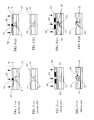
FIGS. 3(a)-3(d) are series of cross-sectional views illustrating a conventional circuit board formation process, in which:
FIG. 3(a) illustrates first via exposure portions formed in the first negative resist;
FIG. 3(b) illustrates an opening formed by the developed first via exposure portion filled with a conductive layer to form a conductive via, and the second negative resist formed after the conductive via;
FIG. 3(c) illustrates the wiring portion of the second negative resist exposed using a misaligned photomask;
FIG. 3(d) illustrates development of the second negative resist which exposes the surface of the conductive via and comes into contact with an adjacent wiring opening, result in a short circuit;
FIGS. 4(a)-4(d) are series of additional cross-sectional views of the method in FIGS. 1 and 2(a)-2(i), for comparison with FIGS. 3(a)-3(d), in which:
FIG. 4(a) illustrates first via exposure portions formed in the first negative resist;
FIG. 4(b) illustrates the second negative resist formed before development of the exposed first negative resist;
FIG. 4(c) illustrates exposure of the wiring portion of the second negative resist using a misaligned photomask during simultaneous development of the first negative resist and the second negative resist; and
FIG. 4(d) illustrates the resulting narrow via opening such that there is no contact with the adjacent wiring opening, resulting in a short circuit less likely to occur.
DETAILED DESCRIPTION
Interposers are currently made primarily using a silicon substrate; however, they are expensive and this limits their use. If interposers could be created using an organic substrate made of an organic material, these costs could be reduced and their application could promote the spread of three-dimensional stacking.
Unfortunately, interposers created with an organic substrate using the methods of the prior art experience certain problems. For example, the dimensions of each type of pattern tend to be unstable due to the properties of organic materials. In addition, exposure and development processes are repeated multiple times, which makes the manufacturing process more complicated. Accordingly, there is a need to solve this problem associated with the creation of organic substrates by providing a method of creating a circuit board with more applications (including wiring board and interposer) even when an organic substrate is used.
A method of creating a circuit board is provided in one aspect of the present invention. This method includes forming a conductive pattern on a substrate; forming a first negative resist on the substrate after formation of the conductive pattern; partially exposing the first negative resist on the surface of the conductive pattern to form a first via exposure portion; forming a second negative resist on the substrate after formation of the first via exposure portion; partially exposing the second negative resist on the first via exposure portion to form a second via exposure portion larger than the first via exposure portion; developing the first negative resist and the second negative resist after formation of the second via exposure portion to form a via opening reaching the conductive pattern; and filling the via opening with a conductive material.
In one aspect of the present invention, simultaneous development of the two negative resists (the first negative resist and the second negative resist) does not remove the two negative resists but rather forms a permanent resist (interlayer insulating layer) which significantly reduces the number of production steps for circuit boards containing conductive vias.
In one aspect of the present invention, forming the second via exposure portion includes simultaneously partially exposing the second negative resist outside of the first via exposure portion to form a conductive wiring exposure portion; forming a via opening reaching the conductive pattern includes simultaneously forming a wiring opening in the second negative resist; and the step of filling the opening with a conductive material includes simultaneously filling the wiring opening with the conductive material.
In one aspect of the present invention, simultaneous formation of the conductive vias and wiring further reduces the number of production steps for circuit boards containing conductive vias, and short circuiting caused by misalignment of conductive vias and wiring can be avoided.
The following is an explanation of an embodiment of the present invention with reference to the drawings. FIG. 1 is a flowchart of a method of forming a circuit board in accordance with an exemplary embodiment of the present invention. FIGS. 2(a)-2(i) are a series of cross-sectional diagrams illustrating the individual operations described in FIG. 1. The following is an explanation of the exemplary method of the present invention and a circuit board obtained using this method with reference to FIG. 1 and FIGS. 2(a)-2(i).
In operation S11 of FIG. 1, a conductive pattern is formed on a substrate. As shown in FIG. 2(a), a conductive pattern 12 is formed on the material (base material) of a substrate 10. The base material can be organic or inorganic insulating material or a semiconducting material such as silicon. The conductive pattern 12 can be obtained by forming a seed layer and patterned resist on the substrate 10, forming a conductive layer such as a copper layer using electroplating, and then removing/etching the remaining resist and seed layer.
In operation S12, a first negative resist is formed on the substrate 10 with the formed conductive pattern 12. As shown in FIG. 2(b), a first negative resist 14 is formed so as to cover the substrate 10 and the surface of the conductive pattern 12. The first negative resist 14 is a so-called negative type photoresist, and is made of a photosensitive material whose exposed portions remain altered. The first negative resist 14 can be formed by using a conventional application technique (spin coating, etc.) using a photosensitive material (resin, polymer material).
In operation S13, a first via exposure portion is formed in the first negative resist 14. As shown in FIG. 2(c), a photomask 16 including unexposed (light-shielding) areas 18 is disposed on the substrate 10, and the first negative resist 14 is exposed to light 20. The photomask 16 is positioned so that the light-shielding areas 18 are directly above the photoresist pattern 12.
The areas 22 of the first negative resist 14 beneath the light-shielding areas 18 of the photomask 16 are not exposed, and these are removed in a subsequent development step (S16) to form first via areas. One characteristic of the method of the present invention is that the first negative resist 14 is not developed immediately after exposure. Direct exposure using a laser beam (laser direct imaging) may be used instead of using a photomask 16.
In operation S14, a second negative resist is formed on top of the first negative resist 14 after exposure. As shown in FIG. 2(d), the second negative resist 24 is formed so that it covers the surface of the exposed first negative resist 14 over the entire substrate 10. The second negative resist 24 can be the same negative type photoresist used for the first negative resist 14, and the same method of formation can be used.
In operation S15, second via exposure portions are formed in the second negative resist 24. As shown in FIG. 2(e), a photomask 26 including light-shielding areas 28 is disposed on the substrate 10, and the second negative resist 24 is exposed to light 20. The photomask 26 is positioned so that the light-shielding areas 28 are directly above the unexposed areas 22 of the first negative resist 14.
The areas 30 of the second negative resist 24 beneath the light-shielding areas 28 of the photomask 26 are not exposed, and these are removed in a subsequent development operation (S16) to form second via (pad) areas on top of the first via areas. A dual damascene structure made of first via exposure areas and second via (pad) exposure areas can be obtained by making the size (inner diameter) of the light-shielding areas 28 of photomask 26 larger than that of the light-shielding areas 18 of photomask 16.
In operation S15, an area to become wiring (conductive pattern) can be exposed at the same time that the second via (pad) exposure portions are formed (exposed). In FIG. 2(e), light-shielding areas 29 of the photomask 26 are provided to form unexposed areas 31 in the second negative resist 24 to form wiring. One characteristic of the method of the present invention is that second via (pad) exposure and wiring exposure are performed at the same time. As explained below with reference to FIG. 3, this can also reduce the likelihood of short circuiting caused by misalignment during exposure.
In operation S16, the exposed first negative resist 14 and second negative resist 24 are developed using a developer. As shown in FIG. 2(f), the development formed via openings 32 in the unexposed areas 22 and 30, and wiring openings 34 in unexposed area 31. The via openings 32 reach the surface of the conductive pattern 12.
One characteristic of the exemplary method in the present invention is that the first negative resist 14 and the second negative resist 24 are not removed but remain to form a permanent resist that functions as an interlayer insulating layer. This reduces the number of development steps and also eliminates the resist removal step.
In operation S17, the via openings 32 and wiring openings 34 formed after development are filled with a conductive material (conductors). An example using a plating method is shown in FIG. 2(g) through 2(i). In FIG. 2(g), a seed layer 36 is formed on the surface of the first negative resist 14 and the second negative resist 24 including the surfaces (inner surfaces) of the via openings 32 and the wiring openings 34. In FIG. 2(h), conductive material (a conductive layer) 38 is formed on the seed layer 36 using electroplating. In this way, the via openings 32 and wiring openings 34 are filled with the conductive material. An example of a conductive material that can be used is copper.
In FIG. 2(i), the surfaces plated with the conductive material 38 are polished to remove the conductive material 38 except for the conductive vias 40 in the via openings 32 and the wiring layer 42 in the wiring openings 34, and to flatten the polished surface. The polishing can be performed using chemical mechanical polishing (CMP) or some other polishing method. For example, an electrodeposition resist can be formed on the conductive material 38 in FIG. 2(h), the surface of the electrodeposition resist can be buffed or chemically etched to flatten the surface, and similar flattening can then performed by removing the remaining electrodeposition resist.
A circuit board structure in which a plurality of the structures shown in FIG. 2(i) have been stacked can be obtained by forming an insulating layer of an organic material on the flattened structure in FIG. 2(i) obtained by performing operations S11 through S17 in FIG. 1 and then repeating operations S11 through S17. A single or stacked circuit board structure can be used as a single circuit board or as a so-called interposer to provide electrical relays between circuit boards or between a circuit board and a semiconductor chip.
The following is an explanation of the advantages of the present invention with reference to FIGS. 3(a)-3(d) and FIGS. 4(a)-4(d). FIGS. 3(a)-3(d) show the processes in the f the prior art in which the via portions and the wiring portions are formed (exposed) separately. In contrast, FIGS. 4(a)-4(d) again show the processes in the method of the present invention in which the via portions and the wiring portions are formed (exposed) simultaneously. FIG. 3(a) of the prior art is the same as FIG. 4(a) of the present invention, and also corresponds to FIG. 2(c). In other words, first via exposure portions (actually unexposed areas) 22 are formed in the first negative resist 14.
In FIG. 3(b), the first via exposure portion 22 formed in FIG. 3(a) is developed to form an opening, the opening is filled with a conductive layer to form a conductive via 44, and the second negative resist 24 is formed. Here, the second resist 24 is formed after the conductive via 44 has been formed. In contrast, FIG. 4(b) of the present invention, as explained above with reference to FIG. 2(d), development or formation of the opening is not performed immediately after the first via exposure portion 22 has been formed.
In FIG. 3(c), the wiring portion of the second negative resist 24 is exposed using a photomask 26. Unexposed areas 30 are formed by the light-shielding portions 28 of the photomask 26. Here, the photomask 26 is misaligned and one of these areas 30 is formed directly above the conductive via 44. Therefore, when the second negative resist 24 is developed, the wiring opening 34 after development exposes the surface of the conductive via 44 as shown in FIG. 3(d), and the conductive via 44 comes into contact with an adjacent wiring opening 35 (see the dotted-line circle indicated by arrow A). As a result, a short circuit later may occur between the conductive layer (wiring layer) filling the wiring opening 35 and the conductive via 44.
However, in the present process, as shown in FIG. 4(c), when exposure of the wiring portion of the second negative resist 24 occurs using a photomask 26, in the event the photomask 26 is misaligned, and one of the areas 30 is formed directly above an exposure area 22 of the via portion, the right side 23 of the first via exposure portion (actually an unexposed area) 22 of the first negative resist 14 is exposed (see the dotted-line circuit indicated by arrow B). As a result, as shown in FIG. 4(d), during simultaneous development of the first negative resist 14 and the second negative resist 24, the via opening 32 is narrow (see the dotted-line circuit indicated by arrow C) so there is no contact with the adjacent wiring opening 35. As a result, a short circuit is less likely to occur later between the conductive layer (wiring layer) filling the wiring opening 35 and the conductive layer (conductive via) filling the via opening 32.
Here, the conductive via formed in the opening 32 has a so-called landless via structure. In order to take into account the narrowing of the width (diameter) of the via opening 32 and avoid an increase in electrical resistance in the conductive via, the width (diameter) of the first via exposure portion 22 may be increased to ensure that the conductive via has the desired width (diameter).
Embodiments of the present invention were explained above with reference to the drawings. However, the present invention is not limited to these embodiments. In addition, the present invention can be embodied in many different ways, including improvements and modifications as well as changes, based on knowledge common in the art without departing from the spirit and scope of the claims.
REFERENCE SIGNS LIST
    • 10: Board (material, substrate)
    • 12: Conductive pattern
    • 14, 24: Negative resist
    • 16, 26: Photomask
    • 18, 28: Light-shielding area
    • 22, 30: Unexposed area
    • 23: Exposed area
    • 32, 34, 35: Opening
    • 36: Seed layer
    • 38: Plated layer
    • 40, 44: Conductive via (pad)
    • 42: Wiring layer

Claims (3)

The invention claimed is:
1. A circuit board, comprising:
a conductive pattern formed on a substrate;
a first negative resist formed on the substrate and the conductive pattern;
the first negative resist having a first via exposure portion formed on the surface of the conductive pattern;
a second negative resist formed on the first negative resist having the first via exposure portion;
the second negative resist having a second via exposure portion formed on the first via exposure portion, the second via exposure portion larger than the first via exposure portion, the first via exposure portion comprising a first sub-portion that overlaps the second via exposure portion and a second sub-portion that does not overlap the second via exposure portion;
a via opening formed corresponding to the location of the first and second via exposure portions defined by concurrent development of the first and second negative resists such that the second via exposure portion is unexposed, and such that the first sub-portion of the first via exposure portion is unexposed, and such that the second sub-portion of the first via exposure portion is exposed, the via opening reaching the conductive pattern; and
the via opening filled with a conductive material.
2. The circuit board of claim 1, wherein the first negative resist and the second negative resist are used as interlayer insulating layers in the circuit board.
3. The circuit board of claim 1, wherein the substrate is an organic substrate, and the circuit board comprises an interposer.
US14/817,378 2014-08-19 2015-08-04 Circuit board formation using organic substrates Expired - Fee Related US9684237B2 (en)

Priority Applications (1)

Application Number Priority Date Filing Date Title
US14/950,673 US9760002B2 (en) 2014-08-19 2015-11-24 Circuit board formation using organic substrates

Applications Claiming Priority (2)

Application Number Priority Date Filing Date Title
JP2014-166328 2014-08-19
JP2014166328A JP6015969B2 (en) 2014-08-19 2014-08-19 Circuit board forming method

Related Child Applications (1)

Application Number Title Priority Date Filing Date
US14/950,673 Continuation US9760002B2 (en) 2014-08-19 2015-11-24 Circuit board formation using organic substrates

Publications (2)

Publication Number Publication Date
US20160057857A1 US20160057857A1 (en) 2016-02-25
US9684237B2 true US9684237B2 (en) 2017-06-20

Family

ID=55349561

Family Applications (2)

Application Number Title Priority Date Filing Date
US14/817,378 Expired - Fee Related US9684237B2 (en) 2014-08-19 2015-08-04 Circuit board formation using organic substrates
US14/950,673 Active US9760002B2 (en) 2014-08-19 2015-11-24 Circuit board formation using organic substrates

Family Applications After (1)

Application Number Title Priority Date Filing Date
US14/950,673 Active US9760002B2 (en) 2014-08-19 2015-11-24 Circuit board formation using organic substrates

Country Status (2)

Country Link
US (2) US9684237B2 (en)
JP (1) JP6015969B2 (en)

Families Citing this family (8)

* Cited by examiner, † Cited by third party
Publication number Priority date Publication date Assignee Title
KR102356809B1 (en) * 2014-12-26 2022-01-28 삼성전기주식회사 Printed circuit board and method of manufacturing the same
KR102579880B1 (en) * 2016-05-12 2023-09-18 삼성전자주식회사 Interposer, semiconductor package, and method of fabricating interposer
CN109037038A (en) * 2017-06-08 2018-12-18 联华电子股份有限公司 The forming method of semiconductor device
KR102321438B1 (en) * 2017-07-28 2021-11-04 엘지이노텍 주식회사 Printed circuit board
JP2019062113A (en) * 2017-09-27 2019-04-18 日立化成株式会社 Manufacturing method of wiring layer
CN109935515B (en) 2017-12-18 2021-07-13 联华电子股份有限公司 Method for forming pattern
JP7211156B2 (en) * 2019-02-27 2023-01-24 凸版印刷株式会社 Multilayer wiring board manufacturing method and multilayer wiring board
US11315890B2 (en) 2020-08-11 2022-04-26 Applied Materials, Inc. Methods of forming microvias with reduced diameter

Citations (14)

* Cited by examiner, † Cited by third party
Publication number Priority date Publication date Assignee Title
US4572764A (en) * 1984-12-13 1986-02-25 E. I. Du Pont De Nemours And Company Preparation of photoformed plastic multistrate by via formation first
US4631111A (en) * 1984-11-27 1986-12-23 E. I. Du Pont De Nemours And Company Dichromic process for preparation of conductive circuit
US4789648A (en) * 1985-10-28 1988-12-06 International Business Machines Corporation Method for producing coplanar multi-level metal/insulator films on a substrate and for forming patterned conductive lines simultaneously with stud vias
US5266446A (en) * 1990-11-15 1993-11-30 International Business Machines Corporation Method of making a multilayer thin film structure
US5480048A (en) * 1992-09-04 1996-01-02 Hitachi, Ltd. Multilayer wiring board fabricating method
US6054251A (en) * 1996-09-25 2000-04-25 Kansai Paint Co., Ltd. Photopolymerizable composition
US20010025414A1 (en) * 2000-03-31 2001-10-04 Toshiyuki Toyoshima Method of producing a multi-layered wiring board
JP2003013313A (en) 2001-07-02 2003-01-15 Toray Ind Inc Warmth-keeping grove
US20030157806A1 (en) * 2001-12-03 2003-08-21 Nec Electronics Corporation Chemical amplification type photoresist composition, method for producing a semiconductor device using the composition , and semiconductor substrate
JP2004040019A (en) 2002-07-08 2004-02-05 Matsushita Electric Ind Co Ltd Method for forming metal wiring
JP2009094412A (en) 2007-10-11 2009-04-30 Sumitomo Chemical Co Ltd Manufacturing method for wiring board, display device and thin-film active-element substrate
US20100044095A1 (en) * 2008-08-19 2010-02-25 International Business Machines Corporation Via Stub Elimination
JP2011003884A (en) 2009-05-20 2011-01-06 Fujitsu Ltd Circuit board and method for manufacturing the same
US20110204523A1 (en) 2010-02-19 2011-08-25 International Business Machines Corporation Method of fabricating dual damascene structures using a multilevel multiple exposure patterning scheme

Patent Citations (14)

* Cited by examiner, † Cited by third party
Publication number Priority date Publication date Assignee Title
US4631111A (en) * 1984-11-27 1986-12-23 E. I. Du Pont De Nemours And Company Dichromic process for preparation of conductive circuit
US4572764A (en) * 1984-12-13 1986-02-25 E. I. Du Pont De Nemours And Company Preparation of photoformed plastic multistrate by via formation first
US4789648A (en) * 1985-10-28 1988-12-06 International Business Machines Corporation Method for producing coplanar multi-level metal/insulator films on a substrate and for forming patterned conductive lines simultaneously with stud vias
US5266446A (en) * 1990-11-15 1993-11-30 International Business Machines Corporation Method of making a multilayer thin film structure
US5480048A (en) * 1992-09-04 1996-01-02 Hitachi, Ltd. Multilayer wiring board fabricating method
US6054251A (en) * 1996-09-25 2000-04-25 Kansai Paint Co., Ltd. Photopolymerizable composition
US20010025414A1 (en) * 2000-03-31 2001-10-04 Toshiyuki Toyoshima Method of producing a multi-layered wiring board
JP2003013313A (en) 2001-07-02 2003-01-15 Toray Ind Inc Warmth-keeping grove
US20030157806A1 (en) * 2001-12-03 2003-08-21 Nec Electronics Corporation Chemical amplification type photoresist composition, method for producing a semiconductor device using the composition , and semiconductor substrate
JP2004040019A (en) 2002-07-08 2004-02-05 Matsushita Electric Ind Co Ltd Method for forming metal wiring
JP2009094412A (en) 2007-10-11 2009-04-30 Sumitomo Chemical Co Ltd Manufacturing method for wiring board, display device and thin-film active-element substrate
US20100044095A1 (en) * 2008-08-19 2010-02-25 International Business Machines Corporation Via Stub Elimination
JP2011003884A (en) 2009-05-20 2011-01-06 Fujitsu Ltd Circuit board and method for manufacturing the same
US20110204523A1 (en) 2010-02-19 2011-08-25 International Business Machines Corporation Method of fabricating dual damascene structures using a multilevel multiple exposure patterning scheme

Non-Patent Citations (2)

* Cited by examiner, † Cited by third party
Title
Hiroyuki Mori et al., "Circuit Board Formation Using Organic Substrates", U.S. Appl. No. 14/950,673, filed Nov. 24, 2015.
List of IBM Patents or Patent Applications Treated as Related; (Appendix P), Filed Feb. 24, 2016; 2 pages.

Also Published As

Publication number Publication date
JP6015969B2 (en) 2016-10-26
US20160081187A1 (en) 2016-03-17
US20160057857A1 (en) 2016-02-25
JP2016042543A (en) 2016-03-31
US9760002B2 (en) 2017-09-12

Similar Documents

Publication Publication Date Title
US9684237B2 (en) Circuit board formation using organic substrates
US9565774B2 (en) Embedded trace substrate and method of forming the same
US9338900B2 (en) Interposer substrate and method of fabricating the same
US7919408B2 (en) Methods for fabricating fine line/space (FLS) routing in high density interconnect (HDI) substrates
US9301405B1 (en) Method for manufacturing microthrough-hole in circuit board and circuit board structure with microthrough-hole
US8058566B2 (en) Packaging substrate structure and manufacturing method thereof
US10602621B1 (en) Method of manufacturing circuit board
US20060243482A1 (en) Circuit board structure and method for fabricating the same
KR20140086535A (en) Circuit board and method for manufacturing the same
CN102214628B (en) Package substrate and fabricating method thereof
US20140042122A1 (en) Method of manufacturing printed circuit board
CN106575623A (en) Pattern between pattern for low profile substrate
KR101840305B1 (en) Interposer for semiconductor package and method of manufacturing the same
US8258009B2 (en) Circuit substrate and manufacturing method thereof and package structure and manufacturing method thereof
TWI607681B (en) Fabrication method for circuit substrate
US8105938B2 (en) Semiconductor substrate and method of manufacturing the same
TWI728410B (en) Circuit board structure and manufacturing method thereof
CN109673099B (en) Multilayer circuit structure and manufacturing method thereof
US10383226B2 (en) Multi-layer circuit structure and manufacturing method thereof
US9735097B1 (en) Package substrate, method for making the same, and package structure having the same
CN114121793B (en) Multilayer metal wiring layer, preparation method thereof and packaging structure
US20230319990A1 (en) Circuit board and manufacturing method thereof
US20230298986A1 (en) Package substrate and manufacturing method thereof
KR101558579B1 (en) Printed circuit board and method for fabricating the same
CN111148373B (en) Method for manufacturing circuit board

Legal Events

Date Code Title Description
AS Assignment

Owner name: INTERNATIONAL BUSINESS MACHINES CORPORATION, NEW Y

Free format text: ASSIGNMENT OF ASSIGNORS INTEREST;ASSIGNORS:MORI, HIROYUKI;NOMA, HIROKAZU;OKAMOTO, KEISHI;REEL/FRAME:036246/0136

Effective date: 20150804

STCF Information on status: patent grant

Free format text: PATENTED CASE

FEPP Fee payment procedure

Free format text: MAINTENANCE FEE REMINDER MAILED (ORIGINAL EVENT CODE: REM.); ENTITY STATUS OF PATENT OWNER: LARGE ENTITY

LAPS Lapse for failure to pay maintenance fees

Free format text: PATENT EXPIRED FOR FAILURE TO PAY MAINTENANCE FEES (ORIGINAL EVENT CODE: EXP.); ENTITY STATUS OF PATENT OWNER: LARGE ENTITY

STCH Information on status: patent discontinuation

Free format text: PATENT EXPIRED DUE TO NONPAYMENT OF MAINTENANCE FEES UNDER 37 CFR 1.362

FP Lapsed due to failure to pay maintenance fee

Effective date: 20210620