US9692429B1 - Systems and methods involving fast-acquisition lock features associated with phase locked loop circuitry - Google Patents
Systems and methods involving fast-acquisition lock features associated with phase locked loop circuitry Download PDFInfo
- Publication number
- US9692429B1 US9692429B1 US14/935,329 US201514935329A US9692429B1 US 9692429 B1 US9692429 B1 US 9692429B1 US 201514935329 A US201514935329 A US 201514935329A US 9692429 B1 US9692429 B1 US 9692429B1
- Authority
- US
- United States
- Prior art keywords
- circuitry
- shift register
- state
- register chain
- logic
- Prior art date
- Legal status (The legal status is an assumption and is not a legal conclusion. Google has not performed a legal analysis and makes no representation as to the accuracy of the status listed.)
- Active
Links
Images


Classifications
-
- H—ELECTRICITY
- H03—ELECTRONIC CIRCUITRY
- H03L—AUTOMATIC CONTROL, STARTING, SYNCHRONISATION, OR STABILISATION OF GENERATORS OF ELECTRONIC OSCILLATIONS OR PULSES
- H03L7/00—Automatic control of frequency or phase; Synchronisation
- H03L7/06—Automatic control of frequency or phase; Synchronisation using a reference signal applied to a frequency- or phase-locked loop
- H03L7/08—Details of the phase-locked loop
- H03L7/085—Details of the phase-locked loop concerning mainly the frequency- or phase-detection arrangement including the filtering or amplification of its output signal
- H03L7/089—Details of the phase-locked loop concerning mainly the frequency- or phase-detection arrangement including the filtering or amplification of its output signal the phase or frequency detector generating up-down pulses
- H03L7/0891—Details of the phase-locked loop concerning mainly the frequency- or phase-detection arrangement including the filtering or amplification of its output signal the phase or frequency detector generating up-down pulses the up-down pulses controlling source and sink current generators, e.g. a charge pump
-
- H—ELECTRICITY
- H03—ELECTRONIC CIRCUITRY
- H03L—AUTOMATIC CONTROL, STARTING, SYNCHRONISATION, OR STABILISATION OF GENERATORS OF ELECTRONIC OSCILLATIONS OR PULSES
- H03L7/00—Automatic control of frequency or phase; Synchronisation
- H03L7/06—Automatic control of frequency or phase; Synchronisation using a reference signal applied to a frequency- or phase-locked loop
- H03L7/08—Details of the phase-locked loop
- H03L7/085—Details of the phase-locked loop concerning mainly the frequency- or phase-detection arrangement including the filtering or amplification of its output signal
- H03L7/087—Details of the phase-locked loop concerning mainly the frequency- or phase-detection arrangement including the filtering or amplification of its output signal using at least two phase detectors or a frequency and phase detector in the loop
-
- H—ELECTRICITY
- H03—ELECTRONIC CIRCUITRY
- H03L—AUTOMATIC CONTROL, STARTING, SYNCHRONISATION, OR STABILISATION OF GENERATORS OF ELECTRONIC OSCILLATIONS OR PULSES
- H03L7/00—Automatic control of frequency or phase; Synchronisation
- H03L7/06—Automatic control of frequency or phase; Synchronisation using a reference signal applied to a frequency- or phase-locked loop
- H03L7/08—Details of the phase-locked loop
- H03L7/085—Details of the phase-locked loop concerning mainly the frequency- or phase-detection arrangement including the filtering or amplification of its output signal
- H03L7/089—Details of the phase-locked loop concerning mainly the frequency- or phase-detection arrangement including the filtering or amplification of its output signal the phase or frequency detector generating up-down pulses
- H03L7/0891—Details of the phase-locked loop concerning mainly the frequency- or phase-detection arrangement including the filtering or amplification of its output signal the phase or frequency detector generating up-down pulses the up-down pulses controlling source and sink current generators, e.g. a charge pump
- H03L7/0895—Details of the current generators
-
- H—ELECTRICITY
- H03—ELECTRONIC CIRCUITRY
- H03L—AUTOMATIC CONTROL, STARTING, SYNCHRONISATION, OR STABILISATION OF GENERATORS OF ELECTRONIC OSCILLATIONS OR PULSES
- H03L7/00—Automatic control of frequency or phase; Synchronisation
- H03L7/06—Automatic control of frequency or phase; Synchronisation using a reference signal applied to a frequency- or phase-locked loop
- H03L7/08—Details of the phase-locked loop
- H03L7/10—Details of the phase-locked loop for assuring initial synchronisation or for broadening the capture range
- H03L7/113—Details of the phase-locked loop for assuring initial synchronisation or for broadening the capture range using frequency discriminator
-
- H—ELECTRICITY
- H03—ELECTRONIC CIRCUITRY
- H03L—AUTOMATIC CONTROL, STARTING, SYNCHRONISATION, OR STABILISATION OF GENERATORS OF ELECTRONIC OSCILLATIONS OR PULSES
- H03L7/00—Automatic control of frequency or phase; Synchronisation
- H03L7/06—Automatic control of frequency or phase; Synchronisation using a reference signal applied to a frequency- or phase-locked loop
- H03L7/08—Details of the phase-locked loop
- H03L7/0807—Details of the phase-locked loop concerning mainly a recovery circuit for the reference signal
Definitions
- aspects of the innovations herein relate generally to fields of clock/data acquisition or handling, such as features involved with clock locking, data locking, clock synthesis, clock data recovery, feedback clocking, and acquiring a quick lock in phase lock loop (PLL) circuitry.
- PLL phase lock loop
- FIGS. 1-3 depicts existing circuitry and background in this regard, with FIG. 1A depicting an existing phase frequency detector and FIG. 3 depicting an existing phase lock loop (PLL) circuit.
- PLL phase lock loop
- the phase frequency detector (PFD) 310 pulls in the frequency and locks in the phase.
- PLL acquisition techniques such as here in FIGS. 1-3 can be unsatisfactory. Among other things, such techniques can be too slow if the preset frequency and target frequency are quite different. Negative gain and cycle slipping issues can also arise.
- phase frequency detector PFD
- PFD phase frequency detector
- Rotational frequency detection typically requires numerous clocks/signals such as internal quadrature clocks (90 degree offset clocks), an I clock (I-clk 902 ), and a Q clock (Q-clk 904 ) as well as latching and comparison of the various states thereof.
- other approaches such as quadricorrelators also involve quadrature clocks, may operate as a function of DC components, and are also an analog solution, thus present associated challenges to adapt to digital circuitry.
- FIG. 1A illustrates a conventional phase frequency detector.
- FIG. 1B depicts an illustrative state diagram showing feedback clock lead and lags.
- FIGS. 2A-2B illustrate how a phase frequency detector affects/pulls clock frequency.
- FIG. 3 illustrates an existing Phase Lock Loop Circuit.
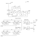
- FIG. 4 depicts an illustrative Digital Frequency Detector aided fast acquisition Phase Locked Loop consistent with aspects related to the innovations herein.
- FIGS. 5A through 5C show illustrative Frequency Detector Implementations consistent with one or more aspects of the innovations herein.
- FIG. 6 depicts an illustrative Time-Domain Waveform of an exemplary Frequency Detector according to the implementation of FIG. 5A consistent with one or more aspects of the innovations herein.
- FIG. 7 shows an illustrative FD+CP 2 current output consistent with one or more aspects of the innovations herein.
- FIG. 8 shows an illustrative Time-Domain Waveform of a Closed-Loop Phase Locked Loop simulation, contrasted with a comparative PFD-only loop system, consistent with aspects of the innovations herein.
- FIGS. 9A-1 through 9A-3 show an illustrative circuit schematic of exemplary frequency detector circuitry consistent with aspects of the innovations herein.
- FIGS. 10A-1 through 10A-3 show another illustrative circuit schematic of exemplary frequency detector circuitry consistent with aspects of the innovations herein.
- FIG. 10B illustrates a detailed diagram of exemplary circuit components and layout of certain frequency detector circuitry, consistent with aspects related to the innovations herein.
- FIGS. 11A and 11B illustrates several elements of the exemplary frequency detector circuitry shown in previous drawings, consistent with aspects of the innovations herein.
- FIGS. 12A-1 through 12C-2 show illustrative circuitry of exemplary charge pump circuits consistent with aspects of the innovations herein.
- FIG. 1A shows a conventional phase frequency detector.
- a conventional PFD may comprise two D flip-flops 110 A, 110 B, an AND gate 112 , and an output 114 .
- the rising edge of reference clock F ref sets output Q to logic “1”.
- “Reset” is logic “1”
- output Q is reset to logic “0”.
- the second flip-flop 110 B is the same circuit but responses to feedback clock.
- a “reset” signal is generated by ‘logic AND’ operation ( 112 ) of “up” 116 and “dn” 118 signals.
- FIG. 1B depicts an illustrative state diagram showing feedback clock lead and lags.
- FIGS. 2A-2B illustrate how a phase frequency detector may affect/pull clock frequency.
- PFD output takes one of the routes in either FIG. 2A or 2B .
- the pull-in current is the average of the PFD output along either route. As such, the pull-in current is small. Further, this current can't change independently to accommodate pull-in process as it affects the lock-in condition.
- FIG. 3 illustrates an existing Phase Lock Loop Circuit with frequency dividers 304 , 306 , a phase frequency detector 310 , a charge pump 312 , a low pass filter 316 and a voltage controlled oscillator (VCO) 318 .
- both the reference clock 302 and the feedback clock 303 are divided by the frequency dividers 304 , 306 .
- the division ratio can be different.
- Charge pump 312 may then adjust “Vcnt” 319 by a charge proportional to the PFD outputs.
- Low pass filter 316 filters out high frequency components and tunes up loop characteristics.
- VCO generates a feedback clock 303 at frequency adjusted by “Vcnt” 319 .
- FIG. 4 depicts illustrative Frequency Detector aided fast acquisition Phase Locked Loop (PLL) circuitry 400 consistent with aspects related to the innovations herein.
- PLL circuitry 400 may comprise voltage controlled oscillator (VCO) circuitry 418 that generates a feedback clock signal, phase frequency detector (PFD) circuitry 410 that receives the feedback clock signal and a reference clock signal, compares a phase of the feedback clock signal to a phase of the reference clock signal, and outputs a phase comparison signal, first charge pump circuitry 412 configured to receive the phase comparison signal and output a control signal proportional to the phase comparison signal to the VCO circuit, frequency detector (FD) circuitry 408 that receives the feedback clock signal and the reference clock signal, and second charge pump circuitry 413 that receives the frequency difference signal and output a control signal proportional to the frequency difference signal to the VCO circuit.
- VCO voltage controlled oscillator
- PFD phase frequency detector
- Frequency detector circuitry 408 that receives the feedback clock signal and the reference clock signal, may be further adapted to compare a frequency of the feedback clock signal to a frequency of the reference clock signal, and output a frequency difference signal that is proportional to a frequency difference between the frequency of the feedback clock and the frequency of the reference clock signal determined by the comparing of the frequencies.
- frequency detector circuitry 408 compares frequency difference of reference clock and feedback clock, with its output being proportional to the frequency difference.
- the second charge pump circuitry 413 charges or discharges “Vcnt” 419 in proportional to the FD circuit 408 output.
- the pull-in current of PFD 410 is small. And PFD affects lock-in condition, so it can't be adjusted freely and independently, e.g., to increase pull-in current.
- the PLL circuitry may utilize frequency detector circuitry 408 such as a digital frequency detector, as set forth in the present disclosure to increase acquisition speed.
- frequency detector circuitry 408 may turn “on” when the frequency of reference clock and feedback clock are very different. When the frequency of reference clock and feedback clock are close enough, FD turns off and allows the PFD loop continues to lock the phase precisely.
- PLL systems and methods herein may detect frequency difference and quickly adjust the frequency of feedback clock.
- a PLL can achieve lock-in condition faster.
- FIG. 5A shows an illustrative frequency detector circuitry implementation consistent with one or more aspects of the innovations herein.
- the first part of the illustrative FD circuit 408 shown includes two (n+1)-bit shift register chains 502 A, 504 A clocked by reference clock and feedback clock, respectively.
- This part of the circuitry may be configured for operation via a sequence of steps such as: (1) initialize, to state “1”, the two shift register chains 502 A, 504 A; (2) shift-in state “0” information via reference clock and feedback clock respectively; and (3) generate, by a “NAND” gate 510 A, a set signal once the last stage output at one of the shift register chain is logic “0”.
- the two shift register chains may be reset to state “1” and may restart the process.
- a second part 514 A of the frequency detector circuitry 408 may include a bit-wise logic operation and a register to latch the result of the logic operation.
- states of shift register chains may be latched via a bit-wise logic operation (k ⁇ i>‘logic and’ !r ⁇ i>).
- a third part of circuit 520 A may include a switchable current source and current sink controlled by the bit-wise outputs from the second part of circuit. All the current sources or the current sinks are connected to node “Vcnt” for adjusting control voltage for VCO output frequency (feedback clock frequency).
- FIGS. 5B and 5C show other illustrative frequency detector circuitry implementations consistent with one or more aspects of the innovations herein.
- the circuit of FIG. 5B may be similar in circuitry and operation to that of FIG. 5A , including shift register chains 502 B, 504 B, as well as comparable second and third parts 514 B, 520 B.
- the polarity of the logic circuit is reversed. Therefore, the shift register chains are initialized to state “0”, and a state “1” shifts in with the reference clock and feedback clock.
- the gate 510 B may generate a set signal once the last stage output at one of the shift register chains reaches logic “1”. Thereafter, the two shift register chains may be reset to state “0”, and the process may be restarted.
- FIG. 6 depicts an illustrative time-domain waveform of an exemplary frequency detector consistent with one or more aspects of the innovations herein.
- all register outputs of the shift register chains e.g., 502 A, 504 A, FIGS. 5A and 5B
- all register outputs of the shift register chains are at logic “1” initially (at point 601 ).
- logic “0” is passed through the register chains.
- last stage output of feedback clock chain 610 becomes logic “0” at point 612
- all outputs in this chain 608 are logic “0”.
- the difference in number of logic “0” implies the difference of frequency.
- the difference in number of logic “0” also decides the charging or discharging current associated with the second charge pump circuitry. The larger difference, for example, may charge or discharge greater current on “Vcnt” node.
- FIG. 7 shows an illustrative frequency detector and second charge pump current output consistent with one or more aspects of the innovations herein.
- the x-axis is the frequency ratio of reference clock and feedback clock. As such, the more that the two frequency differ from each other, the larger the frequency ratio and it generates more FD+CP 2 current output.
- the illustrated line 702 is an approximation curve of the transfer curve. Accordingly, a larger frequency ratio will yield a larger current output of the frequency detector and second charge pump circuitry.
- two (n+1)-bit shift register chains may be clocked by reference clock and feedback clock respectively.
- Exemplary steps may include: initializing the two shift register chains to state “1”, and shifting-in state “0” via the clocks.
- the states of the two chains may then be compared and latched to estimate the frequency ratio of reference clock and feedback clock. With a little delay, the two shift register chains may then be reset to state “1”, to restart the process.
- FIG. 8 shows an illustrative time-domain waveform of a closed-loop phase lock loop representation.
- the PLL circuitry via frequency detection-aided acquisition circuitry, the PLL circuitry is locked much faster, at 810 .
- the frequency detector and second charge pump circuitry generate larger current at larger frequency differentials to decrease the pull-in period, at 808 , while the conventional phase frequency detector and charge pump circuitry merely generates almost constant pull-in current and has associated curve 802 .
- FIGS. 9A-1 through 9A-3 show illustrative circuitry of exemplary frequency detector circuitry consistent with aspects of the innovations herein.
- elements 902 and 904 are the shifter register chains for the feedback clock and reference clock, respectively.
- the output Setb of the delay circuit 906 is then provided to an input of the shift register chain 902 and 904 shown in FIG. 9A-2 that can be replaced by a fixed delay.
- Element 906 is the delay circuit for a “set” signal.
- elements 908 and 910 are the bit-wise logic to compare the states of the two register chains.
- the outputs of elements 908 and 910 are input to elements 912 and 916 , respectively, to latch the compared states.
- Element 914 is the logic for generating “latch” and “set” signals where the output of element 906 is input to element 914 .
- the output of elements 912 and 916 control elements 920 and 922 , respectively, where elements 920 and 922 are the “up”, “dn” signals for controlling the charge pump circuit.
- elements 918 are buffers for “latch” signal.
- FIG. 10B illustrates a detailed diagram of exemplary circuit components of certain frequency detector circuitry, consistent with aspects related to the innovations herein.
- a detailed diagram of exemplary circuit components and layout includes the frequency detector register circuits 1002 , 1004 and latch or delay circuitry 1006 , consistent with aspects related to the innovations herein.
- Elements 1002 and 1004 are the shifter register chains for the feedback clock and reference clock, respectively.
- the output Setb of the delay circuit 1006 is then provided to an input of the shift register chain 1002 and 1004 shown in FIG. 10B .
- delay circuit 1006 may also be replaced by other suitable circuitry such as fixed delay circuitry.
- Element 1006 is the delay circuit for a “set” signal 1008 .
- the output of element 1006 is input to element 914 , set forth above.
- Element 914 is the logic for generating “latch” and “set” signals based on the output of element 1006 .
- FIGS. 10A-1 through 10A-3 show illustrative circuitry of exemplary frequency detector circuitry consistent with aspects of the innovations herein. These figures illustrate an implementation akin to FIGS. 9A-1 through 9A-3 , though pertaining to one illustrative implementation FIG. 5B .
- FIGS. 11A and 11B illustrate several elements of the exemplary frequency detector circuitry shown in previous drawings, consistent with aspects of the innovations herein.
- elements 1102 b and 1104 b are the shifter register chains for feedback clock and reference clock, respectively.
- Element 1114 b is the logic for generating “latch” and “set” signals.
- Element 1106 b is the delay circuit for “set” signal.
- Elements 1108 b and 1110 b are the bit-wise logic to compare the states of the two register chain.
- Elements 1112 b and 1116 b are latching the compared states from 1108 b , 1110 b logic, respectively.
- Elements 1120 and 1122 are the “up”, “dn” signals for controlling charge pump circuit.
- element 1118 are buffers for the “latch” signal.
- FIGS. 12A-1 through 12C-2 show illustrative circuitry of one exemplary second charge pump circuitry (e.g., charge pump circuitry 413 ) consistent with aspects of the innovations herein.
- FIGS. 12A-1 and 12A-2 a high-level drawing of exemplary circuitry is shown, illustrated with a biasing circuit 1230 on the input (left) side of the circuitry and various charging/discharging circuits within 1232 .
- FIGS. 12B-1 and 12B-2 illustrate the transistors and circuit elements of FIG. 12A while further providing various illustrative device sizes/parameters for the exemplary circuit components shown. Referring to all of FIGS.
- elements 1230 represent illustrative biasing circuitry, which may be configured, e.g., to generate constant current source or current sink for charging or discharging “vcnt”.
- element 1232 in FIGS. 12A-1 through 12C-2 illustrates exemplary circuitry branches of charging and discharging path controlled by the “up”, “dn” signals from frequency detector.
- the transfer curve may be controlled, set, or manipulated as a function of the components (e.g., varying the size, ratios, etc. thereof) shown in charging and discharging paths 1234 A and 1234 B in FIGS. 12C-1 and 12C-2 .
- the curve may be adjusted to be non-linear at desired points of the transfer curve/function, such as when the frequency ration of the reference and feedback clocks are close to one.
- FIGS. 9-12 show exemplary circuitry and component values that may be involved with the illustrative implementations depicted, different component and/or values may be utilized consistent with innovations herein.
- features consistent with the present inventions may be implemented via computer-hardware, software and/or firmware.
- the systems and methods disclosed herein may be embodied in various forms including, for example, a data processor, such as a computer that also includes a database, digital electronic circuitry, firmware, software, or in combinations of them.
- a data processor such as a computer that also includes a database
- digital electronic circuitry such as a computer
- firmware such as a firmware
- software such as a computer that also includes a database
- digital electronic circuitry such as a computer that also includes a database
- firmware firmware
- software software
- Such environments and related applications may be specially constructed for performing the various routines, processes and/or operations according to the invention or they may include a general-purpose computer or computing platform selectively activated or reconfigured by code to provide the necessary functionality.
- the processes disclosed herein are not inherently related to any particular computer, network, architecture, environment, or other apparatus, and may be implemented by a suitable combination of hardware, software, and/or firmware.
- various general-purpose machines may be used with programs written in accordance with teachings of the invention, or it may be more convenient to construct a specialized apparatus or system to perform the required methods and techniques.
- aspects of the method and system described herein, such as the logic may be implemented as functionality programmed into any of a variety of circuitry, including programmable logic devices (“PLDs”), such as field programmable gate arrays (“FPGAs”), programmable array logic (“PAL”) devices, electrically programmable logic and memory devices and standard cell-based devices, as well as application specific integrated circuits.
- PLDs programmable logic devices
- FPGAs field programmable gate arrays
- PAL programmable array logic
- Some other possibilities for implementing aspects include: memory devices, microcontrollers with memory (such as EEPROM), embedded microprocessors, firmware, software, etc.
- aspects may be embodied in microprocessors having software-based circuit emulation, discrete logic (sequential and combinatorial), custom devices, fuzzy (neural) logic, quantum devices, and hybrids of any of the above device types.
- the underlying device technologies may be provided in a variety of component types, e.g., metal-oxide semiconductor field-effect transistor (“MOSFET”) technologies like complementary metal-oxide semiconductor (“CMOS”), bipolar technologies like emitter-coupled logic (“ECL”), polymer technologies (e.g., silicon-conjugated polymer and metal-conjugated polymer-metal structures), mixed analog and digital, and so on.
- MOSFET metal-oxide semiconductor field-effect transistor
- CMOS complementary metal-oxide semiconductor
- ECL emitter-coupled logic
- polymer technologies e.g., silicon-conjugated polymer and metal-conjugated polymer-metal structures
- mixed analog and digital and so on.
- Computer-readable media in which such formatted data and/or instructions may be embodied include, but are not limited to, non-volatile storage media in various forms (e.g., optical, magnetic or semiconductor storage media) and carrier waves that may be used to transfer such formatted data and/or instructions through wireless, optical, or wired signaling media or any combination thereof.
- Examples of transfers of such formatted data and/or instructions by carrier waves include, but are not limited to, transfers (uploads, downloads, e-mail, etc.) over the Internet and/or other computer networks via one or more data transfer protocols (e.g., HTTP, FTP, SMTP, and so on).
- transfers uploads, downloads, e-mail, etc.
- data transfer protocols e.g., HTTP, FTP, SMTP, and so on.
- the words “comprise,” “comprising,” and the like are to be construed in an inclusive sense as opposed to an exclusive or exhaustive sense; that is to say, in a sense of “including, but not limited to.” Words using the singular or plural number also include the plural or singular number respectively. Additionally, the words “herein,” “hereunder,” “above,” “below,” and words of similar import refer to this application as a whole and not to any particular portions of this application. When the word “or” is used in reference to a list of two or more items, that word covers all of the following interpretations of the word: any of the items in the list, all of the items in the list and any combination of the items in the list.
Abstract
Systems and methods are disclosed relating to fields of clock/data acquisition or handling, such as clock/data locking and the like. In one exemplary implementation, phase lock loop (PLL) circuitry may comprise voltage controlled oscillator (VCO) circuitry, phase frequency detector, converting circuitry, and frequency detector (FD) circuitry that outputs a frequency difference signal proportional to frequency difference between frequencies of a feedback clock signal and a reference clock signal.
Description
This is a continuation of application Ser. No. 14/082,097, filed Nov. 15, 2013, which claims the benefit/priority of provisional application No. 61/727,058, filed Nov. 15, 2012, all of which are hereby incorporated by reference in entirety.
Field
Aspects of the innovations herein relate generally to fields of clock/data acquisition or handling, such as features involved with clock locking, data locking, clock synthesis, clock data recovery, feedback clocking, and acquiring a quick lock in phase lock loop (PLL) circuitry.
Description of Related Information
Various circuits and techniques are used to achieve lock in phase lock loop circuitry. For example, FIGS. 1-3 depicts existing circuitry and background in this regard, with FIG. 1A depicting an existing phase frequency detector and FIG. 3 depicting an existing phase lock loop (PLL) circuit. In the PLL configuration shown in FIG. 3 , the phase frequency detector (PFD) 310 pulls in the frequency and locks in the phase. However, for a wide-range frequency synthesizer, various PLL acquisition techniques such as here in FIGS. 1-3 can be unsatisfactory. Among other things, such techniques can be too slow if the preset frequency and target frequency are quite different. Negative gain and cycle slipping issues can also arise. When a phase frequency detector (PFD) reaches its limit, for example, one of the clock edges is ignored. This can lead to cycle slipping, which should occur when a second clock edge catches up before the previous clock edge comparison finishes. Further, cycle slipping can occur too early in prior circuitry. For example, cycle slipping may occur as soon as the second clock edge is blocked by the rear edge of the “up”, “down” signals, which can happen too early and even generate a negative gain.
In addition, existing approaches to frequency detection, such as rotational frequency detectors and quadricorrelators, often have limited detection ranges and/or also have a variety of other drawbacks. Rotational frequency detection, for example, typical requires numerous clocks/signals such as internal quadrature clocks (90 degree offset clocks), an I clock (I-clk 902), and a Q clock (Q-clk 904) as well as latching and comparison of the various states thereof. Further, other approaches such as quadricorrelators also involve quadrature clocks, may operate as a function of DC components, and are also an analog solution, thus present associated challenges to adapt to digital circuitry.
Overall, there is a need for systems and methods that may, inter alia, possess improved frequency difference detection, involve fewer clock signals, be digital solutions, more quickly adjust the frequency of a feedback clock, and/or otherwise achieve lock-in condition more quickly with respect to various circuitry.
For a better understanding of the implementations described in this application, reference should be made to the Detailed Description below, in conjunction with the following drawings in which like reference numerals refer to corresponding parts throughout the Figures.
Reference will now be made in detail to implementations of the innovations herein, examples of which are illustrated in the accompanying drawings. In the following detailed description, numerous specific details are set forth in order to provide a sufficient understanding of the subject matter presented herein. But it will be apparent to one of ordinary skill in the art that the subject matter may be practiced without these specific details. Moreover, the particular embodiments described herein are provided by way of example and should not be used to limit the scope of the invention to these particular embodiments. In other instances, well-known data structures, timing protocols, software operations, procedures, and components have not been described in detail so as not to unnecessarily obscure aspects of the embodiments of the present inventions.
The delay time of the loop from each D-flip- flop 110A, 110B and the AND element 112 then back to D-flip-flop has to be long enough to avoid dead zone entailed by the time to full turns on switches (S1, S2) in charge pump. But this also means “Reset” has certain pulse width requirements. When either clock edges falls into “Reset”=logic 1, the clock is blocked in D-flip-flop operation. Such contention may cause, inter alia, the negative gain issue explained above.
Here, frequency detector circuitry 408 compares frequency difference of reference clock and feedback clock, with its output being proportional to the frequency difference. As such, the second charge pump circuitry 413 charges or discharges “Vcnt” 419 in proportional to the FD circuit 408 output. Moreover, as touched on above, the pull-in current of PFD 410 is small. And PFD affects lock-in condition, so it can't be adjusted freely and independently, e.g., to increase pull-in current.
According to implementations herein, the PLL circuitry may utilize frequency detector circuitry 408 such as a digital frequency detector, as set forth in the present disclosure to increase acquisition speed. Here, for example, such frequency detector circuitry 408 may turn “on” when the frequency of reference clock and feedback clock are very different. When the frequency of reference clock and feedback clock are close enough, FD turns off and allows the PFD loop continues to lock the phase precisely.
Overall, via benefits of the frequency detection features and associated circuitry herein, PLL systems and methods herein may detect frequency difference and quickly adjust the frequency of feedback clock. As a function of implementations and innovations involving circuitry herein, such as frequency detector circuitry 408, a PLL can achieve lock-in condition faster.
A second part 514A of the frequency detector circuitry 408 may include a bit-wise logic operation and a register to latch the result of the logic operation. Here, for example, just before shift register chains are reset in step 3, above, states of shift register chains may be latched via a bit-wise logic operation (k<i>‘logic and’ !r<i>).
A third part of circuit 520A may include a switchable current source and current sink controlled by the bit-wise outputs from the second part of circuit. All the current sources or the current sinks are connected to node “Vcnt” for adjusting control voltage for VCO output frequency (feedback clock frequency).
In exemplary implementations consistent with FIG. 7 , two (n+1)-bit shift register chains may be clocked by reference clock and feedback clock respectively. Exemplary steps may include: initializing the two shift register chains to state “1”, and shifting-in state “0” via the clocks. When a state “0” is shifted to the end of either shift register chain, the states of the two chains may then be compared and latched to estimate the frequency ratio of reference clock and feedback clock. With a little delay, the two shift register chains may then be reset to state “1”, to restart the process.
Moreover, it is further noted that while some of FIGS. 9-12 show exemplary circuitry and component values that may be involved with the illustrative implementations depicted, different component and/or values may be utilized consistent with innovations herein.
As disclosed herein, features consistent with the present inventions may be implemented via computer-hardware, software and/or firmware. For example, the systems and methods disclosed herein may be embodied in various forms including, for example, a data processor, such as a computer that also includes a database, digital electronic circuitry, firmware, software, or in combinations of them. Further, while some of the disclosed implementations describe specific hardware components, systems and methods consistent with the innovations herein may be implemented with any combination of hardware, software and/or firmware. Moreover, the above-noted features and other aspects and principles of the innovations herein may be implemented in various environments. Such environments and related applications may be specially constructed for performing the various routines, processes and/or operations according to the invention or they may include a general-purpose computer or computing platform selectively activated or reconfigured by code to provide the necessary functionality. The processes disclosed herein are not inherently related to any particular computer, network, architecture, environment, or other apparatus, and may be implemented by a suitable combination of hardware, software, and/or firmware. For example, various general-purpose machines may be used with programs written in accordance with teachings of the invention, or it may be more convenient to construct a specialized apparatus or system to perform the required methods and techniques.
Aspects of the method and system described herein, such as the logic, may be implemented as functionality programmed into any of a variety of circuitry, including programmable logic devices (“PLDs”), such as field programmable gate arrays (“FPGAs”), programmable array logic (“PAL”) devices, electrically programmable logic and memory devices and standard cell-based devices, as well as application specific integrated circuits. Some other possibilities for implementing aspects include: memory devices, microcontrollers with memory (such as EEPROM), embedded microprocessors, firmware, software, etc. Furthermore, aspects may be embodied in microprocessors having software-based circuit emulation, discrete logic (sequential and combinatorial), custom devices, fuzzy (neural) logic, quantum devices, and hybrids of any of the above device types. The underlying device technologies may be provided in a variety of component types, e.g., metal-oxide semiconductor field-effect transistor (“MOSFET”) technologies like complementary metal-oxide semiconductor (“CMOS”), bipolar technologies like emitter-coupled logic (“ECL”), polymer technologies (e.g., silicon-conjugated polymer and metal-conjugated polymer-metal structures), mixed analog and digital, and so on.
It should also be noted that the various logic and/or functions disclosed herein may be enabled using any number of combinations of hardware, firmware, and/or as data and/or instructions embodied in various machine-readable or computer-readable media, in terms of their behavioral, register transfer, logic component, and/or other characteristics. Computer-readable media in which such formatted data and/or instructions may be embodied include, but are not limited to, non-volatile storage media in various forms (e.g., optical, magnetic or semiconductor storage media) and carrier waves that may be used to transfer such formatted data and/or instructions through wireless, optical, or wired signaling media or any combination thereof. Examples of transfers of such formatted data and/or instructions by carrier waves include, but are not limited to, transfers (uploads, downloads, e-mail, etc.) over the Internet and/or other computer networks via one or more data transfer protocols (e.g., HTTP, FTP, SMTP, and so on).
Unless the context clearly requires otherwise, throughout the description and the claims, the words “comprise,” “comprising,” and the like are to be construed in an inclusive sense as opposed to an exclusive or exhaustive sense; that is to say, in a sense of “including, but not limited to.” Words using the singular or plural number also include the plural or singular number respectively. Additionally, the words “herein,” “hereunder,” “above,” “below,” and words of similar import refer to this application as a whole and not to any particular portions of this application. When the word “or” is used in reference to a list of two or more items, that word covers all of the following interpretations of the word: any of the items in the list, all of the items in the list and any combination of the items in the list.
Although certain presently preferred implementations of the invention have been specifically described herein, it will be apparent to those skilled in the art to which the invention pertains that variations and modifications of the various implementations shown and described herein may be made without departing from the spirit and scope of the invention. Accordingly, it is intended that the invention be limited only to the extent required by the applicable rules of law.
Claims (23)
1. Phase lock loop (PLL) circuitry comprising:
voltage controlled oscillator (VCO) circuitry that generates a feedback clock signal;
phase frequency detector (PFD) circuitry that receives the feedback clock signal and a reference clock signal, compares phase of the feedback clock signal to phase of the reference clock signal, and outputs a phase comparison signal;
first charge pump circuitry that receives the phase comparison signal and outputs, to the VCO circuitry, a control signal proportional to the phase comparison signal;
frequency detector (FD) circuitry that receives the feedback clock signal and the reference clock signal, compares frequency of the feedback clock signal to frequency of the reference clock signal, and outputs a frequency difference signal that is proportional to frequency difference between frequencies of the feedback clock signal and the reference clock signal determined by the comparison;
second charge pump circuitry that receives the frequency difference signal and outputs, to the VCO circuit, a control signal proportional to the frequency difference signal;
wherein the FD circuitry comprises first shift register chain circuitry that receives the reference clock signal; second shift register chain circuitry that receives the feedback clock signal; and gate circuitry that generates a set signal based on an output of the first shift register chain circuit and/or an output of the second shift register chain circuit; and
wherein one or more of:
the first shift register chain circuitry is initialized to a logic 1 state and configured to shift in a logic 0 state when it receives the reference clock signal;
the second shift register chain circuitry is initialized to a logic 1 state and configured to shift in a logic 0 state when it receives the feedback clock signal;
the gate circuitry is configured to generate the set signal when a last stage output of the first shift register chain circuit is logic 0 and/or a last stage output of the second shift register chain circuit is logic 0;
the first shift register chain circuitry is reset to a logic 1 state after the set signal is generated; and/or
the second shift register chain circuitry is reset to a logic 1 state after the set signal is generated.
2. The PLL circuitry of claim 1 , further comprising:
first divider circuitry that divides a primary reference clock signal to output the reference clock signal; and
second divider circuitry that divides a primary feedback clock signal to output the feedback clock signal.
3. The PLL circuitry of claim 1 , further comprising low pass filter (LPF) circuitry that removes one or more high frequency components of the control signal output by the first charge pump circuitry and/or the control signal output by the second charge pump circuitry.
4. The circuitry of claim 3 , wherein the LPF circuitry adjusts a loop stability characteristic of the PLL circuitry, adjusts a response time of the PLL circuitry, and/or adjusts a lock-in time of the PLL circuit.
5. The PLL circuitry of claim 1 , wherein the set signal is an active high signal and/or wherein the register chains are initialized to state “1”, and a state “0” shifts in with the reference clock and feedback clock.
6. The PLL circuitry of claim 1 , wherein the reset signal is an active high signal and/or wherein the register chains are initialized to state “0”, and a state “1” shifts in with the reference clock and feedback clock.
7. The PLL circuitry of claim 1 , wherein:
the first shift register chain circuitry comprises a plurality of D flip-flops;
the second shift register chain circuitry comprises a plurality of D flip-flops; and
the gate circuitry comprises a NAND gate.
8. The PLL circuitry of claim 1 , wherein the FD circuitry further comprises:
bit-wise logic operation and register circuitry that latches a state of the first shift register chain circuitry and a state of the second shift register chain circuitry.
9. The PLL circuitry of claim 8 , wherein the bit-wise logic operation and register circuitry is configured to latch the state of the first shift register chain circuit and the state of the second shift register chain circuit with a bit-wise logic operation.
10. The PLL circuitry of claim 8 , wherein the FD circuitry further comprises:
current generating circuitry comprising a switchable current source and a switchable current sink, the current generating circuit coupled to receive the latched state of the first shift register chain circuitry and the latched state of the second shift register chain circuitry and switch the current source and/or the current sink to generate the frequency difference signal.
11. The PLL circuitry of claim 1 , wherein the FD circuitry further comprises:
bit-wise logic operation and register circuitry that latches a state of the first shift register chain circuitry and a state of the second shift register chain circuitry before the first shift register chain circuitry is reset to a logic 1 state after the set signal is generated and before the second shift register chain circuitry is reset to a logic 1 state.
12. The PLL circuitry of claim 11 , wherein the bit-wise logic operation and register circuitry is configured to latch the state of the first shift register chain circuit and the state of the second shift register chain circuit with a bit-wise logic operation.
13. The PLL circuitry of claim 11 , wherein the FD circuitry further comprises:
current generating circuitry comprising a switchable current source and a switchable current sink, the current generating circuitry coupled to receive the latched state of the first shift register chain circuitry and the latched state of the second shift register chain circuitry and switch the current source and/or the current sink to generate the frequency difference signal.
14. The PLL circuitry of claim 1 , wherein one or more of:
the first shift register chain circuitry is initialized to a logic 0 state and configured to shift in a logic 1 state when it receives the reference clock signal;
the second shift register chain circuitry is initialized to a logic 0 state and configured to shift in a logic 1 state when it receives the feedback clock signal;
the gate circuitry is configured to generate the set signal when a last stage output of the first shift register chain circuit is logic 1 and/or a last stage output of the second shift register chain circuit is logic 1;
the first shift register chain circuitry is reset to a logic 0 state after the set signal is generated; and
the second shift register chain circuitry is reset to a logic 0 state after the set signal is generated.
15. The PLL circuitry of claim 14 , wherein the FD circuitry further comprises:
bit-wise logic operation and register circuitry that latches a state of the first shift register chain circuitry and a state of the second shift register chain circuitry before the first shift register chain circuitry is reset to a logic 0 state after the set signal is generated and before the second shift register chain circuitry is reset to a logic 0 state.
16. The PLL circuitry of claim 15 , or any Hnim hnmin wherein the bit-wise logic operation and register circuit latches the state of the first shift register chain circuitry and the state of the second shift register chain circuitry with a bit-wise logic operation.
17. The PLL circuitry of claim 15 , wherein the FD circuitry further comprises:
current generating circuitry comprising a switchable current source and a switchable current sink, the current generating circuitry coupled to receive the latched state of the first shift register chain circuit and the latched state of the second shift register chain circuit and switch the current source and/or the current sink to generate the frequency difference signal.
18. Phase lock loop (PLL) circuitry comprising:
voltage controlled oscillator (VCO) circuitry that generates a feedback clock signal;
phase frequency detector (PFD) circuitry that receives the feedback clock signal and a reference clock signal, compares phase of the feedback clock signal to phase of the reference clock signal, and outputs a phase comparison signal;
frequency detector (FD) circuitry that receives the feedback clock signal and the reference clock signal, compares frequency of the feedback clock signal to frequency of the reference clock signal, and outputs a frequency difference signal that is proportional to frequency difference between frequencies of the feedback clock signal and the reference clock signal determined by the comparison, wherein the frequency detector circuitry comprises:
first shift register chain circuitry that receives the reference clock signal;
second shift register chain circuitry that receives the feedback clock signal; and
gate circuitry that generates a set signal based on an output of the first shift register chain circuit and/or an output of the second shift register chain circuitry;
converting circuitry that receives the phase comparison signal and/or the frequency difference signal and outputs, to the VCO circuitry, a control signal proportional to the phase comparison signal and/or the frequency difference signal; and
wherein one or more of:
the first shift register chain circuit is initialized to a logic 1 state and configured to shift in a logic 0 state when it receives the reference clock signal;
the second shift register chain circuit is initialized to a logic 1 state and configured to shift in a logic 0 state when it receives the feedback clock signal;
the gate circuit is configured to generate the set signal when a last stage output of the first shift register chain circuit is logic 0 and/or a last stage output of the second shift register chain circuit is logic 0;
the first shift register chain circuit is reset to a logic 1 state after the set signal is generated; and/or
the second shift register chain circuit is reset to a logic 1 state after the set signal is generated.
19. The circuitry of claim 18 , wherein the converting circuitry include charge pump circuitry.
20. The circuitry of claim 18 , further comprising one or more of:
bit-wise logic operation and register circuitry configured to latch a state of the first shift register chain circuit and a state of the second shift register chain circuit with a bit-wise logic operation; and/or
a current generating circuit comprising a switchable current source and a switchable current sink, the current generating circuit being configured to receive the latched state of the first shift register chain circuit and the latched state of the second shift register chain circuit and switch the current source and/or the current sink to generate the frequency difference signal;
first divider circuitry configured to divide a primary reference clock signal to output the reference clock signal;
second divider circuitry configured to divide a primary feedback clock signal to output the feedback clock signal; and/or
LPF circuitry configured to remove one or more high frequency components of the control signal output by the first charge pump and/or the control signal output by the second charge pump, to adjust a loop stability characteristic of the PLL circuit, to adjust a response time of the PLL circuit, and/or to adjust a lock-in time of the PLL circuit.
21. The PLL circuitry of claim 20 , wherein the bit-wise logic operation and register circuitry is configured to latch a state of the first shift register chain circuit and a state of the second shift register chain circuit before the first shift register chain circuit is reset to a logic 0 state after the set signal is generated and before the second shift register chain circuit is reset to a logic 0 state.
22. The PLL circuitry of claim 19 , wherein one or more of:
the first shift register chain circuitry is initialized to a logic 0 state and configured to shift in a logic 1 state when it receives the reference clock signal;
the second shift register chain circuitry is initialized to a logic 0 state and configured to shift in a logic 1 state when it receives the feedback clock signal;
the gate circuitry is configured to generate the set signal when a last stage output of the first shift register chain circuit is logic 1 and/or a last stage output of the second shift register chain circuit is logic 1;
the first shift register chain circuitry is reset to a logic 0 state after the set signal is generated; and/or
the second shift register chain circuitry is reset to a logic 0 state after the set signal is generated.
23. The PLL circuitry of claim 21 , wherein the bit-wise logic operation and register circuit is configured to latch a state of the first shift register chain circuit and a state of the second shift register chain circuit before the first shift register chain circuit is reset to a logic 1 state after the set signal is generated and before the second shift register chain circuit is reset to a logic 1 state.
Priority Applications (3)
| Application Number | Priority Date | Filing Date | Title |
|---|---|---|---|
| US14/935,329 US9692429B1 (en) | 2012-11-15 | 2015-11-06 | Systems and methods involving fast-acquisition lock features associated with phase locked loop circuitry |
| US15/442,375 US9859902B2 (en) | 2012-11-15 | 2017-02-24 | Systems and method involving fast-acquisition lock features associated with phase locked loop circuitry |
| US15/853,558 US20180123603A1 (en) | 2012-11-15 | 2017-12-22 | Systems and method involving fast-acquisition lock features associated with phase locked loop circuitry |
Applications Claiming Priority (3)
| Application Number | Priority Date | Filing Date | Title |
|---|---|---|---|
| US201261727058P | 2012-11-15 | 2012-11-15 | |
| US201314082097A | 2013-11-15 | 2013-11-15 | |
| US14/935,329 US9692429B1 (en) | 2012-11-15 | 2015-11-06 | Systems and methods involving fast-acquisition lock features associated with phase locked loop circuitry |
Related Parent Applications (1)
| Application Number | Title | Priority Date | Filing Date |
|---|---|---|---|
| US201314082097A Continuation | 2012-11-15 | 2013-11-15 |
Related Child Applications (1)
| Application Number | Title | Priority Date | Filing Date |
|---|---|---|---|
| US15/442,375 Division US9859902B2 (en) | 2012-11-15 | 2017-02-24 | Systems and method involving fast-acquisition lock features associated with phase locked loop circuitry |
Publications (1)
| Publication Number | Publication Date |
|---|---|
| US9692429B1 true US9692429B1 (en) | 2017-06-27 |
Family
ID=58800459
Family Applications (3)
| Application Number | Title | Priority Date | Filing Date |
|---|---|---|---|
| US14/935,329 Active US9692429B1 (en) | 2012-11-15 | 2015-11-06 | Systems and methods involving fast-acquisition lock features associated with phase locked loop circuitry |
| US15/442,375 Active US9859902B2 (en) | 2012-11-15 | 2017-02-24 | Systems and method involving fast-acquisition lock features associated with phase locked loop circuitry |
| US15/853,558 Abandoned US20180123603A1 (en) | 2012-11-15 | 2017-12-22 | Systems and method involving fast-acquisition lock features associated with phase locked loop circuitry |
Family Applications After (2)
| Application Number | Title | Priority Date | Filing Date |
|---|---|---|---|
| US15/442,375 Active US9859902B2 (en) | 2012-11-15 | 2017-02-24 | Systems and method involving fast-acquisition lock features associated with phase locked loop circuitry |
| US15/853,558 Abandoned US20180123603A1 (en) | 2012-11-15 | 2017-12-22 | Systems and method involving fast-acquisition lock features associated with phase locked loop circuitry |
Country Status (1)
| Country | Link |
|---|---|
| US (3) | US9692429B1 (en) |
Cited By (16)
| Publication number | Priority date | Publication date | Assignee | Title |
|---|---|---|---|---|
| US20170163269A1 (en) * | 2012-11-15 | 2017-06-08 | Gsi Technology, Inc. | Systems and method involving fast-acquisition lock features associated with phase locked loop circuitry |
| US10521229B2 (en) | 2016-12-06 | 2019-12-31 | Gsi Technology, Inc. | Computational memory cell and processing array device using memory cells |
| US10651861B2 (en) | 2018-10-15 | 2020-05-12 | Analog Devices, Inc. | Filterless digital phase-locked loop |
| US10770133B1 (en) | 2016-12-06 | 2020-09-08 | Gsi Technology, Inc. | Read and write data processing circuits and methods associated with computational memory cells that provides write inhibits and read bit line pre-charge inhibits |
| US10777262B1 (en) | 2016-12-06 | 2020-09-15 | Gsi Technology, Inc. | Read data processing circuits and methods associated memory cells |
| US10847212B1 (en) | 2016-12-06 | 2020-11-24 | Gsi Technology, Inc. | Read and write data processing circuits and methods associated with computational memory cells using two read multiplexers |
| US10847213B1 (en) | 2016-12-06 | 2020-11-24 | Gsi Technology, Inc. | Write data processing circuits and methods associated with computational memory cells |
| US10854284B1 (en) | 2016-12-06 | 2020-12-01 | Gsi Technology, Inc. | Computational memory cell and processing array device with ratioless write port |
| US10860320B1 (en) | 2016-12-06 | 2020-12-08 | Gsi Technology, Inc. | Orthogonal data transposition system and method during data transfers to/from a processing array |
| US10877731B1 (en) | 2019-06-18 | 2020-12-29 | Gsi Technology, Inc. | Processing array device that performs one cycle full adder operation and bit line read/write logic features |
| US10891076B1 (en) | 2016-12-06 | 2021-01-12 | Gsi Technology, Inc. | Results processing circuits and methods associated with computational memory cells |
| US10930341B1 (en) | 2019-06-18 | 2021-02-23 | Gsi Technology, Inc. | Processing array device that performs one cycle full adder operation and bit line read/write logic features |
| US10943648B1 (en) | 2016-12-06 | 2021-03-09 | Gsi Technology, Inc. | Ultra low VDD memory cell with ratioless write port |
| US10958272B2 (en) | 2019-06-18 | 2021-03-23 | Gsi Technology, Inc. | Computational memory cell and processing array device using complementary exclusive or memory cells |
| US10998040B2 (en) | 2016-12-06 | 2021-05-04 | Gsi Technology, Inc. | Computational memory cell and processing array device using the memory cells for XOR and XNOR computations |
| US11227653B1 (en) | 2016-12-06 | 2022-01-18 | Gsi Technology, Inc. | Storage array circuits and methods for computational memory cells |
Families Citing this family (2)
| Publication number | Priority date | Publication date | Assignee | Title |
|---|---|---|---|---|
| KR20210141813A (en) * | 2020-05-13 | 2021-11-23 | 삼성디스플레이 주식회사 | Clock data recovery circuit, display device, and method of operating a clock data recovery circuit |
| US11595047B1 (en) * | 2022-03-03 | 2023-02-28 | Ciena Corporation | Apparatus and methods for a phase frequency detector with a wide operational range |
Citations (55)
| Publication number | Priority date | Publication date | Assignee | Title |
|---|---|---|---|---|
| US4308505A (en) | 1979-06-13 | 1981-12-29 | Trw, Inc. | Frequency detector device and method |
| US4587496A (en) | 1984-09-12 | 1986-05-06 | General Signal Corporation | Fast acquisition phase-lock loop |
| US4594564A (en) | 1984-06-11 | 1986-06-10 | Signetics Corporation | Frequency detector for use with phase locked loop |
| US5302916A (en) | 1992-12-21 | 1994-04-12 | At&T Bell Laboratories | Wide range digital frequency detector |
| US5744991A (en) | 1995-10-16 | 1998-04-28 | Altera Corporation | System for distributing clocks using a delay lock loop in a programmable logic circuit |
| US5969986A (en) | 1998-06-23 | 1999-10-19 | Invox Technology | High-bandwidth read and write architectures for non-volatile memories |
| US6100721A (en) * | 1999-02-01 | 2000-08-08 | Motorola, Inc. | Circuit and method of extending the linear range of a phase frequency detector |
| US6262937B1 (en) | 1998-03-13 | 2001-07-17 | Cypress Semiconductor Corp. | Synchronous random access memory having a read/write address bus and process for writing to and reading from the same |
| US6407642B2 (en) * | 2000-01-07 | 2002-06-18 | Matsushita Electric Industrial Co., Ltd. | Frequency detector and phase-locked loop circuit including the detector |
| US6448757B2 (en) | 1996-06-28 | 2002-09-10 | Curtin University Of Technology | Precise digital frequency detection |
| US6504417B1 (en) | 2001-08-15 | 2003-01-07 | International Business Machines Corporation | Active trim circuit for CMOS on-chip resistors |
| US6642747B1 (en) * | 2002-03-15 | 2003-11-04 | National Semiconductor Corporation | Frequency detector for a phase locked loop system |
| US6683930B1 (en) | 1999-12-23 | 2004-01-27 | Cypress Semiconductor Corp. | Digital phase/frequency detector, and clock generator and data recovery PLL containing the same |
| US6744277B1 (en) | 2001-05-06 | 2004-06-01 | Altera Corporation | Programmable current reference circuit |
| US20040169565A1 (en) | 2003-02-27 | 2004-09-02 | Richard Gaggl | Tuning circuit for a filter |
| US20050024912A1 (en) | 2003-07-28 | 2005-02-03 | Mosaic Systems, Inc. | System and method for providing a redundant memory array in a semiconductor memory integrated circuit |
| US6853696B1 (en) | 1999-12-20 | 2005-02-08 | Nortel Networks Limited | Method and apparatus for clock recovery and data qualification |
| US6859107B1 (en) | 2001-09-05 | 2005-02-22 | Silicon Image, Inc. | Frequency comparator with hysteresis between locked and unlocked conditions |
| US6882237B2 (en) | 2003-04-30 | 2005-04-19 | Zarlink Semiconductor Inc. | Capture range control mechanism for voltage controlled oscillators |
| US20050186930A1 (en) | 1999-10-21 | 2005-08-25 | Ahmadreza Rofougaran | Adaptive radio transceiver with offset PLL with subsampling mixers |
| US6954091B2 (en) | 2003-11-25 | 2005-10-11 | Lsi Logic Corporation | Programmable phase-locked loop |
| US7042271B2 (en) | 2004-05-06 | 2006-05-09 | Broadcom Corporation | Resistor compensation apparatus |
| US20060139105A1 (en) | 2004-12-28 | 2006-06-29 | Adrian Maxim | Method and apparatus to achieve a process, temperature and divider modulus independent PLL loop bandwidth and damping factor using open-loop calibration techniques |
| US7142477B1 (en) | 2004-06-18 | 2006-11-28 | Cypress Semiconductor Corp. | Memory interface system and method for reducing cycle time of sequential read and write accesses using separate address and data buses |
| US7152009B2 (en) | 2002-11-29 | 2006-12-19 | Matsushita Electric Industrial Co., Ltd. | Parameter correction circuit and parameter correction method |
| US7218157B2 (en) * | 2002-08-30 | 2007-05-15 | Nxp B.V. | Phase locked loop |
| US20070109030A1 (en) * | 2004-04-26 | 2007-05-17 | Samsung Electronics Co., Ltd. | Phase-Locked Loop Integrated Circuits Having Fast Phase Locking Characteristics |
| US20070229129A1 (en) | 2006-03-28 | 2007-10-04 | Nec Corporation | Pll circuit |
| US7282999B2 (en) | 2004-07-30 | 2007-10-16 | Infineon Technologies Ag | Method and device for generating a clock signal using a phase difference signal and a feedback signal |
| US20080068096A1 (en) | 2006-02-28 | 2008-03-20 | Feng Kai D | Frequency divider monitor of phase lock loop |
| US7349515B1 (en) | 2003-09-22 | 2008-03-25 | Cypress Semiconductor Corporation | Method and an apparatus to improve production yield of phase locked loops |
| US7369000B2 (en) * | 2004-04-15 | 2008-05-06 | Mediatek Incorporation | Adaptive frequency detector of phase locked loop |
| US7439816B1 (en) * | 2005-09-28 | 2008-10-21 | Cypress Semiconductor Corporation | Phase-locked loop fast lock circuit and method |
| US7545223B2 (en) | 2006-09-14 | 2009-06-09 | Nec Electronics Corporation | PLL circuit |
| US7577225B2 (en) | 2005-07-28 | 2009-08-18 | Agere Systems Inc. | Digital phase-looked loop |
| US7592847B2 (en) * | 2007-03-22 | 2009-09-22 | Mediatek Inc. | Phase frequency detector and phase-locked loop |
| US20090256642A1 (en) * | 2008-04-09 | 2009-10-15 | John Paul Lesso | Locked-loop circuit |
| US7622996B2 (en) | 2006-09-07 | 2009-11-24 | Realtek Semiconductor Corp. | Multi-loop phase locked loop circuit |
| US7633322B1 (en) | 2007-04-06 | 2009-12-15 | Altera Corporation | Digital loop circuit for programmable logic device |
| US20100085086A1 (en) | 2008-07-29 | 2010-04-08 | Fujitsu Limited | Digital Frequency Detector |
| US7728675B1 (en) * | 2006-03-31 | 2010-06-01 | Cypress Semiconductor Corporation | Fast lock circuit for a phase lock loop |
| US7737743B1 (en) * | 2008-03-07 | 2010-06-15 | National Semiconductor Corporation | Phase-locked loop including sampling phase detector and charge pump with pulse width control |
| US7812644B2 (en) | 2007-06-25 | 2010-10-12 | Samsung Electronics Co., Ltd. | Digital frequency detector and digital phase locked loop using the digital frequency detector |
| US7830212B2 (en) * | 2007-07-30 | 2010-11-09 | Mediatek Inc. | Phase locked loop, voltage controlled oscillator, and phase-frequency detector |
| US7843239B2 (en) | 2008-01-02 | 2010-11-30 | Samsung Electronics Co., Ltd. | Dividing circuit and phase locked loop using the same |
| US7848725B2 (en) | 2007-07-02 | 2010-12-07 | Broadcom Corporation | RF transmitter with stable on-chip PLL |
| US7940088B1 (en) | 2009-03-31 | 2011-05-10 | Pmc-Sierra, Inc. | High speed phase frequency detector |
| US7944256B2 (en) | 2007-03-07 | 2011-05-17 | Hitachi, Ltd. | Semiconductor integrated circuit device |
| US7965108B2 (en) | 2007-04-26 | 2011-06-21 | Mediatek Inc. | Frequency synthesizer |
| US8044724B2 (en) | 2008-09-22 | 2011-10-25 | Mosys, Inc. | Low jitter large frequency tuning LC PLL for multi-speed clocking applications |
| US8063707B2 (en) | 2009-05-08 | 2011-11-22 | Mediatek Inc. | Phase locked loop |
| US20120153999A1 (en) | 2010-12-17 | 2012-06-21 | Kwan-Dong Kim | Clock signal generation circuit |
| US8242820B2 (en) | 2009-12-28 | 2012-08-14 | Hynix Semiconductor Inc. | Phase locked loop and method for operating the same |
| US8692621B2 (en) * | 2011-12-21 | 2014-04-08 | Fairchild Semiconductor Corporation | Methods and apparatus for oscillator frequency calibration |
| US9053768B2 (en) | 2013-03-14 | 2015-06-09 | Gsi Technology, Inc. | Systems and methods of pipelined output latching involving synchronous memory arrays |
Family Cites Families (4)
| Publication number | Priority date | Publication date | Assignee | Title |
|---|---|---|---|---|
| US4741006A (en) * | 1984-07-12 | 1988-04-26 | Kabushiki Kaisha Toshiba | Up/down counter device with reduced number of discrete circuit elements |
| US4856035A (en) * | 1988-05-26 | 1989-08-08 | Raytheon Company | CMOS binary up/down counter |
| JP3292188B2 (en) * | 1999-11-10 | 2002-06-17 | 日本電気株式会社 | PLL circuit |
| US9692429B1 (en) * | 2012-11-15 | 2017-06-27 | Gsi Technology, Inc. | Systems and methods involving fast-acquisition lock features associated with phase locked loop circuitry |
-
2015
- 2015-11-06 US US14/935,329 patent/US9692429B1/en active Active
-
2017
- 2017-02-24 US US15/442,375 patent/US9859902B2/en active Active
- 2017-12-22 US US15/853,558 patent/US20180123603A1/en not_active Abandoned
Patent Citations (59)
| Publication number | Priority date | Publication date | Assignee | Title |
|---|---|---|---|---|
| US4308505A (en) | 1979-06-13 | 1981-12-29 | Trw, Inc. | Frequency detector device and method |
| US4594564A (en) | 1984-06-11 | 1986-06-10 | Signetics Corporation | Frequency detector for use with phase locked loop |
| US4587496A (en) | 1984-09-12 | 1986-05-06 | General Signal Corporation | Fast acquisition phase-lock loop |
| US5302916A (en) | 1992-12-21 | 1994-04-12 | At&T Bell Laboratories | Wide range digital frequency detector |
| US5744991A (en) | 1995-10-16 | 1998-04-28 | Altera Corporation | System for distributing clocks using a delay lock loop in a programmable logic circuit |
| US6448757B2 (en) | 1996-06-28 | 2002-09-10 | Curtin University Of Technology | Precise digital frequency detection |
| US6262937B1 (en) | 1998-03-13 | 2001-07-17 | Cypress Semiconductor Corp. | Synchronous random access memory having a read/write address bus and process for writing to and reading from the same |
| US5969986A (en) | 1998-06-23 | 1999-10-19 | Invox Technology | High-bandwidth read and write architectures for non-volatile memories |
| US6100721A (en) * | 1999-02-01 | 2000-08-08 | Motorola, Inc. | Circuit and method of extending the linear range of a phase frequency detector |
| US20050186930A1 (en) | 1999-10-21 | 2005-08-25 | Ahmadreza Rofougaran | Adaptive radio transceiver with offset PLL with subsampling mixers |
| US6853696B1 (en) | 1999-12-20 | 2005-02-08 | Nortel Networks Limited | Method and apparatus for clock recovery and data qualification |
| US6683930B1 (en) | 1999-12-23 | 2004-01-27 | Cypress Semiconductor Corp. | Digital phase/frequency detector, and clock generator and data recovery PLL containing the same |
| US6407642B2 (en) * | 2000-01-07 | 2002-06-18 | Matsushita Electric Industrial Co., Ltd. | Frequency detector and phase-locked loop circuit including the detector |
| US6744277B1 (en) | 2001-05-06 | 2004-06-01 | Altera Corporation | Programmable current reference circuit |
| US6504417B1 (en) | 2001-08-15 | 2003-01-07 | International Business Machines Corporation | Active trim circuit for CMOS on-chip resistors |
| US6859107B1 (en) | 2001-09-05 | 2005-02-22 | Silicon Image, Inc. | Frequency comparator with hysteresis between locked and unlocked conditions |
| US6642747B1 (en) * | 2002-03-15 | 2003-11-04 | National Semiconductor Corporation | Frequency detector for a phase locked loop system |
| US7218157B2 (en) * | 2002-08-30 | 2007-05-15 | Nxp B.V. | Phase locked loop |
| US7152009B2 (en) | 2002-11-29 | 2006-12-19 | Matsushita Electric Industrial Co., Ltd. | Parameter correction circuit and parameter correction method |
| US7002404B2 (en) | 2003-02-27 | 2006-02-21 | Infineon Technologies Ag | Tuning circuit for a filter |
| US20040169565A1 (en) | 2003-02-27 | 2004-09-02 | Richard Gaggl | Tuning circuit for a filter |
| US6882237B2 (en) | 2003-04-30 | 2005-04-19 | Zarlink Semiconductor Inc. | Capture range control mechanism for voltage controlled oscillators |
| US20050024912A1 (en) | 2003-07-28 | 2005-02-03 | Mosaic Systems, Inc. | System and method for providing a redundant memory array in a semiconductor memory integrated circuit |
| US7349515B1 (en) | 2003-09-22 | 2008-03-25 | Cypress Semiconductor Corporation | Method and an apparatus to improve production yield of phase locked loops |
| US6954091B2 (en) | 2003-11-25 | 2005-10-11 | Lsi Logic Corporation | Programmable phase-locked loop |
| US7369000B2 (en) * | 2004-04-15 | 2008-05-06 | Mediatek Incorporation | Adaptive frequency detector of phase locked loop |
| US20070109030A1 (en) * | 2004-04-26 | 2007-05-17 | Samsung Electronics Co., Ltd. | Phase-Locked Loop Integrated Circuits Having Fast Phase Locking Characteristics |
| US7042271B2 (en) | 2004-05-06 | 2006-05-09 | Broadcom Corporation | Resistor compensation apparatus |
| US7142477B1 (en) | 2004-06-18 | 2006-11-28 | Cypress Semiconductor Corp. | Memory interface system and method for reducing cycle time of sequential read and write accesses using separate address and data buses |
| US7282999B2 (en) | 2004-07-30 | 2007-10-16 | Infineon Technologies Ag | Method and device for generating a clock signal using a phase difference signal and a feedback signal |
| US20060139105A1 (en) | 2004-12-28 | 2006-06-29 | Adrian Maxim | Method and apparatus to achieve a process, temperature and divider modulus independent PLL loop bandwidth and damping factor using open-loop calibration techniques |
| US7095287B2 (en) | 2004-12-28 | 2006-08-22 | Silicon Laboratories Inc. | Method and apparatus to achieve a process, temperature and divider modulus independent PLL loop bandwidth and damping factor using open-loop calibration techniques |
| US7577225B2 (en) | 2005-07-28 | 2009-08-18 | Agere Systems Inc. | Digital phase-looked loop |
| US7439816B1 (en) * | 2005-09-28 | 2008-10-21 | Cypress Semiconductor Corporation | Phase-locked loop fast lock circuit and method |
| US7920665B1 (en) | 2005-09-28 | 2011-04-05 | Cypress Semiconductor Corporation | Symmetrical range controller circuit and method |
| US20080068096A1 (en) | 2006-02-28 | 2008-03-20 | Feng Kai D | Frequency divider monitor of phase lock loop |
| US20070229129A1 (en) | 2006-03-28 | 2007-10-04 | Nec Corporation | Pll circuit |
| US7728675B1 (en) * | 2006-03-31 | 2010-06-01 | Cypress Semiconductor Corporation | Fast lock circuit for a phase lock loop |
| US7622996B2 (en) | 2006-09-07 | 2009-11-24 | Realtek Semiconductor Corp. | Multi-loop phase locked loop circuit |
| US7545223B2 (en) | 2006-09-14 | 2009-06-09 | Nec Electronics Corporation | PLL circuit |
| US7944256B2 (en) | 2007-03-07 | 2011-05-17 | Hitachi, Ltd. | Semiconductor integrated circuit device |
| US7592847B2 (en) * | 2007-03-22 | 2009-09-22 | Mediatek Inc. | Phase frequency detector and phase-locked loop |
| US7633322B1 (en) | 2007-04-06 | 2009-12-15 | Altera Corporation | Digital loop circuit for programmable logic device |
| US7965108B2 (en) | 2007-04-26 | 2011-06-21 | Mediatek Inc. | Frequency synthesizer |
| US7812644B2 (en) | 2007-06-25 | 2010-10-12 | Samsung Electronics Co., Ltd. | Digital frequency detector and digital phase locked loop using the digital frequency detector |
| US7848725B2 (en) | 2007-07-02 | 2010-12-07 | Broadcom Corporation | RF transmitter with stable on-chip PLL |
| US7830212B2 (en) * | 2007-07-30 | 2010-11-09 | Mediatek Inc. | Phase locked loop, voltage controlled oscillator, and phase-frequency detector |
| US20110018597A1 (en) | 2007-07-30 | 2011-01-27 | Mediatek Inc. | Phase Locked Loop and Phase-Frequency Detector |
| US7843239B2 (en) | 2008-01-02 | 2010-11-30 | Samsung Electronics Co., Ltd. | Dividing circuit and phase locked loop using the same |
| US7737743B1 (en) * | 2008-03-07 | 2010-06-15 | National Semiconductor Corporation | Phase-locked loop including sampling phase detector and charge pump with pulse width control |
| US20090256642A1 (en) * | 2008-04-09 | 2009-10-15 | John Paul Lesso | Locked-loop circuit |
| US20100085086A1 (en) | 2008-07-29 | 2010-04-08 | Fujitsu Limited | Digital Frequency Detector |
| US8044724B2 (en) | 2008-09-22 | 2011-10-25 | Mosys, Inc. | Low jitter large frequency tuning LC PLL for multi-speed clocking applications |
| US7940088B1 (en) | 2009-03-31 | 2011-05-10 | Pmc-Sierra, Inc. | High speed phase frequency detector |
| US8063707B2 (en) | 2009-05-08 | 2011-11-22 | Mediatek Inc. | Phase locked loop |
| US8242820B2 (en) | 2009-12-28 | 2012-08-14 | Hynix Semiconductor Inc. | Phase locked loop and method for operating the same |
| US20120153999A1 (en) | 2010-12-17 | 2012-06-21 | Kwan-Dong Kim | Clock signal generation circuit |
| US8692621B2 (en) * | 2011-12-21 | 2014-04-08 | Fairchild Semiconductor Corporation | Methods and apparatus for oscillator frequency calibration |
| US9053768B2 (en) | 2013-03-14 | 2015-06-09 | Gsi Technology, Inc. | Systems and methods of pipelined output latching involving synchronous memory arrays |
Cited By (27)
| Publication number | Priority date | Publication date | Assignee | Title |
|---|---|---|---|---|
| US20170163269A1 (en) * | 2012-11-15 | 2017-06-08 | Gsi Technology, Inc. | Systems and method involving fast-acquisition lock features associated with phase locked loop circuitry |
| US9859902B2 (en) * | 2012-11-15 | 2018-01-02 | Gsi Technology, Inc. | Systems and method involving fast-acquisition lock features associated with phase locked loop circuitry |
| US11094374B1 (en) | 2016-12-06 | 2021-08-17 | Gsi Technology, Inc. | Write data processing circuits and methods associated with computational memory cells |
| US11194519B2 (en) | 2016-12-06 | 2021-12-07 | Gsi Technology, Inc. | Results processing circuits and methods associated with computational memory cells |
| US11763881B2 (en) | 2016-12-06 | 2023-09-19 | Gsi Technology, Inc. | Computational memory cell and processing array device using the memory cells for XOR and XNOR computations |
| US10770133B1 (en) | 2016-12-06 | 2020-09-08 | Gsi Technology, Inc. | Read and write data processing circuits and methods associated with computational memory cells that provides write inhibits and read bit line pre-charge inhibits |
| US10943648B1 (en) | 2016-12-06 | 2021-03-09 | Gsi Technology, Inc. | Ultra low VDD memory cell with ratioless write port |
| US10847212B1 (en) | 2016-12-06 | 2020-11-24 | Gsi Technology, Inc. | Read and write data processing circuits and methods associated with computational memory cells using two read multiplexers |
| US10847213B1 (en) | 2016-12-06 | 2020-11-24 | Gsi Technology, Inc. | Write data processing circuits and methods associated with computational memory cells |
| US11409528B2 (en) | 2016-12-06 | 2022-08-09 | Gsi Technology, Inc. | Orthogonal data transposition system and method during data transfers to/from a processing array |
| US10860318B2 (en) | 2016-12-06 | 2020-12-08 | Gsi Technology, Inc. | Computational memory cell and processing array device using memory cells |
| US10860320B1 (en) | 2016-12-06 | 2020-12-08 | Gsi Technology, Inc. | Orthogonal data transposition system and method during data transfers to/from a processing array |
| US11257540B2 (en) | 2016-12-06 | 2022-02-22 | Gsi Technology, Inc. | Write data processing methods associated with computational memory cells |
| US10891076B1 (en) | 2016-12-06 | 2021-01-12 | Gsi Technology, Inc. | Results processing circuits and methods associated with computational memory cells |
| US10725777B2 (en) | 2016-12-06 | 2020-07-28 | Gsi Technology, Inc. | Computational memory cell and processing array device using memory cells |
| US10777262B1 (en) | 2016-12-06 | 2020-09-15 | Gsi Technology, Inc. | Read data processing circuits and methods associated memory cells |
| US10854284B1 (en) | 2016-12-06 | 2020-12-01 | Gsi Technology, Inc. | Computational memory cell and processing array device with ratioless write port |
| US10998040B2 (en) | 2016-12-06 | 2021-05-04 | Gsi Technology, Inc. | Computational memory cell and processing array device using the memory cells for XOR and XNOR computations |
| US10521229B2 (en) | 2016-12-06 | 2019-12-31 | Gsi Technology, Inc. | Computational memory cell and processing array device using memory cells |
| US11150903B2 (en) | 2016-12-06 | 2021-10-19 | Gsi Technology, Inc. | Computational memory cell and processing array device using memory cells |
| US11227653B1 (en) | 2016-12-06 | 2022-01-18 | Gsi Technology, Inc. | Storage array circuits and methods for computational memory cells |
| US11205476B1 (en) | 2016-12-06 | 2021-12-21 | Gsi Technology, Inc. | Read data processing circuits and methods associated with computational memory cells |
| US10651861B2 (en) | 2018-10-15 | 2020-05-12 | Analog Devices, Inc. | Filterless digital phase-locked loop |
| US11194548B2 (en) | 2019-06-18 | 2021-12-07 | Gsi Technology, Inc. | Processing array device that performs one cycle full adder operation and bit line read/write logic features |
| US10877731B1 (en) | 2019-06-18 | 2020-12-29 | Gsi Technology, Inc. | Processing array device that performs one cycle full adder operation and bit line read/write logic features |
| US10958272B2 (en) | 2019-06-18 | 2021-03-23 | Gsi Technology, Inc. | Computational memory cell and processing array device using complementary exclusive or memory cells |
| US10930341B1 (en) | 2019-06-18 | 2021-02-23 | Gsi Technology, Inc. | Processing array device that performs one cycle full adder operation and bit line read/write logic features |
Also Published As
| Publication number | Publication date |
|---|---|
| US20180123603A1 (en) | 2018-05-03 |
| US20170163269A1 (en) | 2017-06-08 |
| US9859902B2 (en) | 2018-01-02 |
Similar Documents
| Publication | Publication Date | Title |
|---|---|---|
| US9859902B2 (en) | Systems and method involving fast-acquisition lock features associated with phase locked loop circuitry | |
| TWI489783B (en) | Clock generator with phase interpolation and method for the same | |
| US9608651B1 (en) | Systems and methods of phase-locked loop involving closed-loop, continuous frequency range, auto calibration and/or other features | |
| US7839177B1 (en) | Techniques for phase detection with fast reset | |
| US7053666B2 (en) | Phase frequency detector | |
| US9413295B1 (en) | Systems and methods of phase frequency detection with clock edge overriding reset, extending detection range, improvement of cycle slipping and/or other features | |
| US9509296B1 (en) | Systems and methods of phase frequency detection involving features such as improved clock edge handling circuitry/aspects | |
| US9160353B2 (en) | Phase frequency detector and charge pump for phase lock loop fast-locking | |
| US20100259305A1 (en) | Injection locked phase lock loops | |
| US8686768B2 (en) | Phase locked loop | |
| US8575966B2 (en) | Method of operating phase-lock assistant circuitry | |
| Lad Kirankumar et al. | A dead-zone-free zero blind-zone high-speed phase frequency detector for charge-pump PLL | |
| US8786315B2 (en) | Phase frequency detector | |
| Cheng et al. | A difference detector PFD for low jitter PLL | |
| Hati et al. | A PFD and Charge Pump switching circuit to optimize the output phase noise of the PLL in 0.13-µm CMOS | |
| US8035453B1 (en) | Techniques relating to oscillators | |
| KR20120012386A (en) | Lock detection circuit and phase-locked loop circuit including the same | |
| TWI416877B (en) | Charge pumper and phase-detecting apparatus, phase-locked loop and delay-locked loop using the same | |
| Stojčev et al. | Clock aligner based on delay locked loop with double edge synchronization | |
| Babazadeh et al. | A high-speed and wide detectable frequency range phase detector for DLLs | |
| KR20140090455A (en) | Phase locked loop circuit | |
| Patel et al. | Design and analysis of phase-locked loop and performance parameters | |
| Ranjan | Design and analysis of differential multiphase DLL for jitter and power optimization | |
| Dulari et al. | Design and Imple-mentation of Alias-Locked Loop in 90nm Technology for RF Applications | |
| Kim et al. | An unlimited lock range DLL for clock generator |
Legal Events
| Date | Code | Title | Description |
|---|---|---|---|
| AS | Assignment |
Owner name: GSI TECHNOLOGY, INC., CALIFORNIA Free format text: ASSIGNMENT OF ASSIGNORS INTEREST;ASSIGNOR:CHANG, CHAO-HUNG;REEL/FRAME:037006/0568 Effective date: 20151109 |
|
| STCF | Information on status: patent grant |
Free format text: PATENTED CASE |
|
| MAFP | Maintenance fee payment |
Free format text: PAYMENT OF MAINTENANCE FEE, 4TH YR, SMALL ENTITY (ORIGINAL EVENT CODE: M2551); ENTITY STATUS OF PATENT OWNER: SMALL ENTITY Year of fee payment: 4 |