US9748438B2 - Nanostructure semiconductor light emitting device - Google Patents
Nanostructure semiconductor light emitting device Download PDFInfo
- Publication number
- US9748438B2 US9748438B2 US15/190,406 US201615190406A US9748438B2 US 9748438 B2 US9748438 B2 US 9748438B2 US 201615190406 A US201615190406 A US 201615190406A US 9748438 B2 US9748438 B2 US 9748438B2
- Authority
- US
- United States
- Prior art keywords
- light emitting
- layer
- quantum well
- forming
- conductivity
- Prior art date
- Legal status (The legal status is an assumption and is not a legal conclusion. Google has not performed a legal analysis and makes no representation as to the accuracy of the status listed.)
- Active
Links
Images


Classifications
-
- H—ELECTRICITY
- H01—ELECTRIC ELEMENTS
- H01L—SEMICONDUCTOR DEVICES NOT COVERED BY CLASS H10
- H01L33/00—Semiconductor devices with at least one potential-jump barrier or surface barrier specially adapted for light emission; Processes or apparatus specially adapted for the manufacture or treatment thereof or of parts thereof; Details thereof
- H01L33/005—Processes
- H01L33/0062—Processes for devices with an active region comprising only III-V compounds
- H01L33/0066—Processes for devices with an active region comprising only III-V compounds with a substrate not being a III-V compound
- H01L33/007—Processes for devices with an active region comprising only III-V compounds with a substrate not being a III-V compound comprising nitride compounds
-
- H—ELECTRICITY
- H01—ELECTRIC ELEMENTS
- H01L—SEMICONDUCTOR DEVICES NOT COVERED BY CLASS H10
- H01L33/00—Semiconductor devices with at least one potential-jump barrier or surface barrier specially adapted for light emission; Processes or apparatus specially adapted for the manufacture or treatment thereof or of parts thereof; Details thereof
- H01L33/02—Semiconductor devices with at least one potential-jump barrier or surface barrier specially adapted for light emission; Processes or apparatus specially adapted for the manufacture or treatment thereof or of parts thereof; Details thereof characterised by the semiconductor bodies
- H01L33/04—Semiconductor devices with at least one potential-jump barrier or surface barrier specially adapted for light emission; Processes or apparatus specially adapted for the manufacture or treatment thereof or of parts thereof; Details thereof characterised by the semiconductor bodies with a quantum effect structure or superlattice, e.g. tunnel junction
- H01L33/06—Semiconductor devices with at least one potential-jump barrier or surface barrier specially adapted for light emission; Processes or apparatus specially adapted for the manufacture or treatment thereof or of parts thereof; Details thereof characterised by the semiconductor bodies with a quantum effect structure or superlattice, e.g. tunnel junction within the light emitting region, e.g. quantum confinement structure or tunnel barrier
-
- B—PERFORMING OPERATIONS; TRANSPORTING
- B82—NANOTECHNOLOGY
- B82Y—SPECIFIC USES OR APPLICATIONS OF NANOSTRUCTURES; MEASUREMENT OR ANALYSIS OF NANOSTRUCTURES; MANUFACTURE OR TREATMENT OF NANOSTRUCTURES
- B82Y20/00—Nanooptics, e.g. quantum optics or photonic crystals
-
- H—ELECTRICITY
- H01—ELECTRIC ELEMENTS
- H01L—SEMICONDUCTOR DEVICES NOT COVERED BY CLASS H10
- H01L33/00—Semiconductor devices with at least one potential-jump barrier or surface barrier specially adapted for light emission; Processes or apparatus specially adapted for the manufacture or treatment thereof or of parts thereof; Details thereof
- H01L33/02—Semiconductor devices with at least one potential-jump barrier or surface barrier specially adapted for light emission; Processes or apparatus specially adapted for the manufacture or treatment thereof or of parts thereof; Details thereof characterised by the semiconductor bodies
- H01L33/08—Semiconductor devices with at least one potential-jump barrier or surface barrier specially adapted for light emission; Processes or apparatus specially adapted for the manufacture or treatment thereof or of parts thereof; Details thereof characterised by the semiconductor bodies with a plurality of light emitting regions, e.g. laterally discontinuous light emitting layer or photoluminescent region integrated within the semiconductor body
-
- H—ELECTRICITY
- H01—ELECTRIC ELEMENTS
- H01L—SEMICONDUCTOR DEVICES NOT COVERED BY CLASS H10
- H01L33/00—Semiconductor devices with at least one potential-jump barrier or surface barrier specially adapted for light emission; Processes or apparatus specially adapted for the manufacture or treatment thereof or of parts thereof; Details thereof
- H01L33/02—Semiconductor devices with at least one potential-jump barrier or surface barrier specially adapted for light emission; Processes or apparatus specially adapted for the manufacture or treatment thereof or of parts thereof; Details thereof characterised by the semiconductor bodies
- H01L33/20—Semiconductor devices with at least one potential-jump barrier or surface barrier specially adapted for light emission; Processes or apparatus specially adapted for the manufacture or treatment thereof or of parts thereof; Details thereof characterised by the semiconductor bodies with a particular shape, e.g. curved or truncated substrate
- H01L33/24—Semiconductor devices with at least one potential-jump barrier or surface barrier specially adapted for light emission; Processes or apparatus specially adapted for the manufacture or treatment thereof or of parts thereof; Details thereof characterised by the semiconductor bodies with a particular shape, e.g. curved or truncated substrate of the light emitting region, e.g. non-planar junction
-
- H—ELECTRICITY
- H01—ELECTRIC ELEMENTS
- H01L—SEMICONDUCTOR DEVICES NOT COVERED BY CLASS H10
- H01L33/00—Semiconductor devices with at least one potential-jump barrier or surface barrier specially adapted for light emission; Processes or apparatus specially adapted for the manufacture or treatment thereof or of parts thereof; Details thereof
- H01L33/02—Semiconductor devices with at least one potential-jump barrier or surface barrier specially adapted for light emission; Processes or apparatus specially adapted for the manufacture or treatment thereof or of parts thereof; Details thereof characterised by the semiconductor bodies
- H01L33/26—Materials of the light emitting region
- H01L33/30—Materials of the light emitting region containing only elements of group III and group V of the periodic system
- H01L33/32—Materials of the light emitting region containing only elements of group III and group V of the periodic system containing nitrogen
-
- H—ELECTRICITY
- H01—ELECTRIC ELEMENTS
- H01L—SEMICONDUCTOR DEVICES NOT COVERED BY CLASS H10
- H01L33/00—Semiconductor devices with at least one potential-jump barrier or surface barrier specially adapted for light emission; Processes or apparatus specially adapted for the manufacture or treatment thereof or of parts thereof; Details thereof
- H01L33/48—Semiconductor devices with at least one potential-jump barrier or surface barrier specially adapted for light emission; Processes or apparatus specially adapted for the manufacture or treatment thereof or of parts thereof; Details thereof characterised by the semiconductor body packages
- H01L33/52—Encapsulations
-
- F—MECHANICAL ENGINEERING; LIGHTING; HEATING; WEAPONS; BLASTING
- F21—LIGHTING
- F21K—NON-ELECTRIC LIGHT SOURCES USING LUMINESCENCE; LIGHT SOURCES USING ELECTROCHEMILUMINESCENCE; LIGHT SOURCES USING CHARGES OF COMBUSTIBLE MATERIAL; LIGHT SOURCES USING SEMICONDUCTOR DEVICES AS LIGHT-GENERATING ELEMENTS; LIGHT SOURCES NOT OTHERWISE PROVIDED FOR
- F21K9/00—Light sources using semiconductor devices as light-generating elements, e.g. using light-emitting diodes [LED] or lasers
- F21K9/20—Light sources comprising attachment means
- F21K9/23—Retrofit light sources for lighting devices with a single fitting for each light source, e.g. for substitution of incandescent lamps with bayonet or threaded fittings
- F21K9/232—Retrofit light sources for lighting devices with a single fitting for each light source, e.g. for substitution of incandescent lamps with bayonet or threaded fittings specially adapted for generating an essentially omnidirectional light distribution, e.g. with a glass bulb
-
- F—MECHANICAL ENGINEERING; LIGHTING; HEATING; WEAPONS; BLASTING
- F21—LIGHTING
- F21Y—INDEXING SCHEME ASSOCIATED WITH SUBCLASSES F21K, F21L, F21S and F21V, RELATING TO THE FORM OR THE KIND OF THE LIGHT SOURCES OR OF THE COLOUR OF THE LIGHT EMITTED
- F21Y2115/00—Light-generating elements of semiconductor light sources
- F21Y2115/10—Light-emitting diodes [LED]
-
- H—ELECTRICITY
- H01—ELECTRIC ELEMENTS
- H01L—SEMICONDUCTOR DEVICES NOT COVERED BY CLASS H10
- H01L2224/00—Indexing scheme for arrangements for connecting or disconnecting semiconductor or solid-state bodies and methods related thereto as covered by H01L24/00
- H01L2224/01—Means for bonding being attached to, or being formed on, the surface to be connected, e.g. chip-to-package, die-attach, "first-level" interconnects; Manufacturing methods related thereto
- H01L2224/42—Wire connectors; Manufacturing methods related thereto
- H01L2224/47—Structure, shape, material or disposition of the wire connectors after the connecting process
- H01L2224/48—Structure, shape, material or disposition of the wire connectors after the connecting process of an individual wire connector
- H01L2224/4805—Shape
- H01L2224/4809—Loop shape
- H01L2224/48091—Arched
-
- H—ELECTRICITY
- H01—ELECTRIC ELEMENTS
- H01L—SEMICONDUCTOR DEVICES NOT COVERED BY CLASS H10
- H01L2224/00—Indexing scheme for arrangements for connecting or disconnecting semiconductor or solid-state bodies and methods related thereto as covered by H01L24/00
- H01L2224/01—Means for bonding being attached to, or being formed on, the surface to be connected, e.g. chip-to-package, die-attach, "first-level" interconnects; Manufacturing methods related thereto
- H01L2224/42—Wire connectors; Manufacturing methods related thereto
- H01L2224/47—Structure, shape, material or disposition of the wire connectors after the connecting process
- H01L2224/48—Structure, shape, material or disposition of the wire connectors after the connecting process of an individual wire connector
- H01L2224/481—Disposition
- H01L2224/48151—Connecting between a semiconductor or solid-state body and an item not being a semiconductor or solid-state body, e.g. chip-to-substrate, chip-to-passive
- H01L2224/48221—Connecting between a semiconductor or solid-state body and an item not being a semiconductor or solid-state body, e.g. chip-to-substrate, chip-to-passive the body and the item being stacked
- H01L2224/48245—Connecting between a semiconductor or solid-state body and an item not being a semiconductor or solid-state body, e.g. chip-to-substrate, chip-to-passive the body and the item being stacked the item being metallic
- H01L2224/48247—Connecting between a semiconductor or solid-state body and an item not being a semiconductor or solid-state body, e.g. chip-to-substrate, chip-to-passive the body and the item being stacked the item being metallic connecting the wire to a bond pad of the item
-
- H—ELECTRICITY
- H01—ELECTRIC ELEMENTS
- H01L—SEMICONDUCTOR DEVICES NOT COVERED BY CLASS H10
- H01L2224/00—Indexing scheme for arrangements for connecting or disconnecting semiconductor or solid-state bodies and methods related thereto as covered by H01L24/00
- H01L2224/01—Means for bonding being attached to, or being formed on, the surface to be connected, e.g. chip-to-package, die-attach, "first-level" interconnects; Manufacturing methods related thereto
- H01L2224/42—Wire connectors; Manufacturing methods related thereto
- H01L2224/47—Structure, shape, material or disposition of the wire connectors after the connecting process
- H01L2224/48—Structure, shape, material or disposition of the wire connectors after the connecting process of an individual wire connector
- H01L2224/481—Disposition
- H01L2224/48151—Connecting between a semiconductor or solid-state body and an item not being a semiconductor or solid-state body, e.g. chip-to-substrate, chip-to-passive
- H01L2224/48221—Connecting between a semiconductor or solid-state body and an item not being a semiconductor or solid-state body, e.g. chip-to-substrate, chip-to-passive the body and the item being stacked
- H01L2224/48245—Connecting between a semiconductor or solid-state body and an item not being a semiconductor or solid-state body, e.g. chip-to-substrate, chip-to-passive the body and the item being stacked the item being metallic
- H01L2224/48257—Connecting between a semiconductor or solid-state body and an item not being a semiconductor or solid-state body, e.g. chip-to-substrate, chip-to-passive the body and the item being stacked the item being metallic connecting the wire to a die pad of the item
-
- H—ELECTRICITY
- H01—ELECTRIC ELEMENTS
- H01L—SEMICONDUCTOR DEVICES NOT COVERED BY CLASS H10
- H01L2924/00—Indexing scheme for arrangements or methods for connecting or disconnecting semiconductor or solid-state bodies as covered by H01L24/00
- H01L2924/0001—Technical content checked by a classifier
- H01L2924/00014—Technical content checked by a classifier the subject-matter covered by the group, the symbol of which is combined with the symbol of this group, being disclosed without further technical details
-
- H—ELECTRICITY
- H01—ELECTRIC ELEMENTS
- H01L—SEMICONDUCTOR DEVICES NOT COVERED BY CLASS H10
- H01L2933/00—Details relating to devices covered by the group H01L33/00 but not provided for in its subgroups
- H01L2933/0008—Processes
- H01L2933/0033—Processes relating to semiconductor body packages
-
- H—ELECTRICITY
- H01—ELECTRIC ELEMENTS
- H01L—SEMICONDUCTOR DEVICES NOT COVERED BY CLASS H10
- H01L2933/00—Details relating to devices covered by the group H01L33/00 but not provided for in its subgroups
- H01L2933/0008—Processes
- H01L2933/0033—Processes relating to semiconductor body packages
- H01L2933/005—Processes relating to semiconductor body packages relating to encapsulations
-
- H—ELECTRICITY
- H01—ELECTRIC ELEMENTS
- H01L—SEMICONDUCTOR DEVICES NOT COVERED BY CLASS H10
- H01L2933/00—Details relating to devices covered by the group H01L33/00 but not provided for in its subgroups
- H01L2933/0008—Processes
- H01L2933/0033—Processes relating to semiconductor body packages
- H01L2933/0058—Processes relating to semiconductor body packages relating to optical field-shaping elements
Definitions
- the present disclosure relates to a nanostructure semiconductor light emitting device.
- semiconductor light emitting devices using nanostructures have improved crystallinity, and/or may have active layers obtained from non-polar or semi-polar planes, thereby reducing or preventing luminous efficiency from deteriorating due to polarization.
- such nanostructure semiconductor light emitting devices can emit light through a significantly large surface area, resulting in improved luminous efficiency.
- problematic indium incorporation inside the active layers may be caused during a growth process, resulting in difficulties in emitting longer-wavelength light.
- An aspect of the present disclosure may provide a nanostructure semiconductor light emitting device having improved internal quantum efficiency and capable of converting the wavelength of emitted light into a relatively long wavelength.
- FIG. 1 is a schematic perspective view of a nanostructure semiconductor light emitting device according to at least one example embodiment in the present disclosure
- FIG. 2 is a cross-sectional view of the nanostructure semiconductor light emitting device illustrated in FIG. 1 ;
- FIG. 3 is an enlarged view illustrating a stacked structure, taken along line X1-X1′, in the nanostructure semiconductor light emitting device illustrated in FIGS. 1 and 2 ;
- FIG. 4 is a graph illustrating indium (In) composition ratios in a thickness direction of an active layer used in the nanostructure semiconductor light emitting device illustrated in FIG. 1 ;
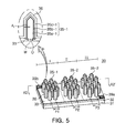
- FIG. 5 is a schematic perspective view of a nanostructure semiconductor light emitting device according to at least one example embodiment in the present disclosure
- FIG. 6 is a cross-sectional view of the nanostructure semiconductor light emitting device illustrated in FIG. 5 , taken along line X 2 -X 2 ′;
- FIG. 7 is a plan view illustrating a pattern of openings in a mask usable in the example embodiment of FIG. 5 ;
- FIGS. 8A through 8C are graphs illustrating In composition ratios in a thickness direction of active layers used for respective groups in the nanostructure semiconductor light emitting device illustrated in FIG. 5 ;
- FIG. 9 is a cross-sectional view of a nanostructure semiconductor light emitting device according to at least one example embodiment in the present disclosure.
- FIGS. 10A and 10B are graphs illustrating In composition ratios in a thickness direction of blue and green active layers used in a nanostructure semiconductor light emitting device according to comparative example 1;
- FIGS. 11A and 11B are graphs illustrating In composition ratios in a thickness direction of blue and green active layers used in a nanostructure semiconductor light emitting device according to inventive example 1;
- FIG. 12 is a graph illustrating photo-luminance results of blue and green active layers used in nanostructure semiconductor light emitting devices according to inventive example 2 and comparative example 2;
- FIGS. 13A and 13B are time charts related to the control of growth temperature and source gas flow in a process of growing quantum wells usable in at least one example embodiment in the present disclosure
- FIG. 14 is a graph illustrating In change rates in the quantum well of FIGS. 13A and 13B ;
- FIG. 15 is a graph illustrating internal quantum efficiency and wavelength difference according to thicknesses of regions having a high In composition ratio, as the results of experiment 3;
- FIG. 16 is a graph illustrating wavelength changes according to pitches of nanocores, as the results of experiment 4.
- FIGS. 17A through 17C are graphs illustrating various examples of In change rates in a quantum well
- FIGS. 18A and 18B are graphs illustrating various examples of In change rates in a quantum well
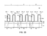
- FIGS. 19 through 25 are cross-sectional views illustrating a method of manufacturing a nanostructure semiconductor light emitting device according to an example embodiment in the present disclosure
- FIGS. 26A and 26B are side cross-sectional views illustrating examples of a mask including openings
- FIGS. 27A and 27B are views illustrating heat treatment or regrowth processes applicable to the processes illustrated in FIGS. 22 and 23 ;
- FIGS. 28 through 31 are cross-sectional views illustrating a method of manufacturing a nanostructure semiconductor light emitting device according to another example embodiment in the present disclosure.
- FIG. 32 is a cross-sectional view of a semiconductor light emitting device package including a nanostructure semiconductor light emitting device according to an example embodiment in the present disclosure
- FIGS. 33 and 34 illustrate examples of a backlight unit including a nanostructure semiconductor light emitting device according to an example embodiment in the present disclosure
- FIG. 35 illustrates an example of a lighting device including a nanostructure semiconductor light emitting device according to an example embodiment in the present disclosure.
- FIG. 36 illustrates an example of a headlamp including a nanostructure semiconductor light emitting device according to an example embodiment in the present disclosure.
- inventive concepts will now be described more fully hereinafter with reference to the accompanying drawings, in which example embodiments of the inventive concepts are shown.
- inventive concepts are not limited to the following example embodiments, and may be implemented in various forms. Accordingly, the example embodiments are provided only to disclose the inventive concepts and let those skilled in the art know the category of the inventive concepts.
- embodiments of the inventive concepts are not limited to the specific examples provided herein and are exaggerated for clarity.
- example embodiments are described herein with reference to cross-sectional illustrations and/or plane illustrations that are idealized example illustrations. Accordingly, variations from the shapes of the illustrations as a result, for example, of manufacturing techniques and/or tolerances, are to be expected. Thus, example embodiments should not be construed as limited to the shapes of regions illustrated herein but are to include deviations in shapes that result, for example, from manufacturing. For example, an etching region illustrated as a rectangle will, typically, have rounded or curved features. Thus, the regions illustrated in the figures are schematic in nature and their shapes are not intended to illustrate the actual shape of a region of a device and are not intended to limit the scope of example embodiments.
- devices and methods of forming devices according to various embodiments described herein may be embodied in microelectronic devices such as integrated circuits, wherein a plurality of devices according to various embodiments described herein are integrated in the same microelectronic device. Accordingly, the cross-sectional view(s) illustrated herein may be replicated in two different directions, which need not be orthogonal, in the microelectronic device.
- a plan view of the microelectronic device that embodies devices according to various embodiments described herein may include a plurality of the devices in an array and/or in a two-dimensional pattern that is based on the functionality of the microelectronic device.
- microelectronic devices according to various embodiments described herein may be interspersed among other devices depending on the functionality of the microelectronic device. Moreover, microelectronic devices according to various embodiments described herein may be replicated in a third direction that may be orthogonal to the two different directions, to provide three-dimensional integrated circuits.
- the cross-sectional view(s) illustrated herein provide support for a plurality of devices according to various embodiments described herein that extend along two different directions in a plan view and/or in three different directions in a perspective view.
- the device/structure may include a plurality of active regions and transistor structures (or memory cell structures, gate structures, etc., as appropriate to the case) thereon, as would be illustrated by a plan view of the device/structure.
- FIG. 1 is a schematic perspective view of a nanostructure semiconductor light emitting device according to an example embodiment in the present disclosure
- FIG. 2 is a cross-sectional view of the nanostructure semiconductor light emitting device illustrated in FIG. 1 .
- a nanostructure semiconductor light emitting device 10 may include a base layer 12 formed of a first conductivity-type semiconductor material and a plurality of light emitting nanostructures 15 disposed on the base layer 12 .
- the nanostructure semiconductor light emitting device 10 may include a substrate 11 having an upper surface on which the base layer 12 is disposed. A convex pattern including uneven portions R may be formed on the upper surface of the substrate 11 . The uneven portions R may improve light extraction efficiency and/or the quality of a single crystal grown thereon.
- the substrate 11 may be an insulating substrate, a conductive substrate or a semiconductor substrate.
- the substrate 11 may be formed of sapphire, SiC, Si, MgAl 2 O 4 , MgO, LiALO 2 , LiGaO 2 or GaN.
- the base layer 12 may include a first-conductivity type nitride semiconductor layer and may provide a growth surface for the light emitting nanostructures 15 .
- the base layer 12 may be formed of a nitride semiconductor containing Al x In y Ga 1-x-y N (0 ⁇ x ⁇ 1, 0 ⁇ y ⁇ 1, 0 ⁇ x+y ⁇ 1) and may be doped with n-type impurities such as silicon (Si).
- the base layer 12 may be an n-type GaN layer.
- An insulating layer 13 having openings therein may be formed on the base layer 12 and the openings may be provided to facilitate growth of the light emitting nanostructures 15 (for example, nanocores 15 a ). Portions of the base layer 12 may be exposed through the openings and the nanocores 15 a may be formed on the exposed portions of the base layer 12 .
- the insulating layer 13 may be used as a mask for growth of the nanocores 15 a .
- the insulating layer 13 may be formed of an insulating material such as SiO 2 or SiN x .
- Each of the light emitting nanostructures 15 may include a main portion M having a hexagonal prism structure and a tip portion T disposed on the top of the main portion M.
- the main portion M of the light emitting nanostructure 15 may have side surfaces, each of which having a first crystal plane, and the tip portion T of the light emitting nanostructure 15 may have a second crystal plane different from the first crystal plane.
- the tip portion T of the light emitting nanostructure 15 may have a hexagonal pyramid structure.
- the shape of the light emitting nanostructure 15 may be determined depending on the shape of the nanocore 15 a , and the structure of the nanocore 15 a may be divided into the main portion M and the tip portion T.
- the light emitting nanostructure 15 may include the nanocore 15 a formed of a first conductivity-type semiconductor material, and an active layer 15 b and a second conductivity-type semiconductor layer 15 c sequentially formed on a surface of the nanocore 15 a.
- FIG. 3 is an enlarged view of a portion of the light emitting nanostructure of FIGS. 1 and 2 , taken along line X 1 -X 1 ′, to illustrate a stacked structure.
- the nanocore 15 a may be formed of a nitride semiconductor containing Al x In y Ga 1-x-y N (0 ⁇ x ⁇ 1, 0 ⁇ y ⁇ 1, 0 ⁇ x+y ⁇ 1), similar to the base layer 12 .
- the nanocore 15 a may be formed of n-type GaN.
- the second conductivity-type semiconductor layer 15 c may be formed of a nitride semiconductor containing p-type Al x In y Ga 1-x-y N (0 ⁇ x ⁇ 1, 0 ⁇ y ⁇ 1, 0 ⁇ x+y ⁇ 1), and may include a plurality of layers as necessary.
- the second conductivity-type semiconductor layer 15 c may include a p-type AlGaN layer 15 c ′, a p-type GaN layer 15 c ′′ having low concentration of p-type impurities, and a p-type GaN layer 15 c ′′′ having a higher concentration of p-type impurities.
- the p-type AlGaN layer 15 c ′ and the p-type GaN layer 15 c ′′′ having high concentration of p-type impurities may be provided as an electron blocking layer (EBL) and a contact layer, respectively.
- EBL electron blocking layer
- the active layer 15 b used in the at least one example embodiment may have a multi-quantum well (MQW) structure in which a plurality of quantum wells 15 b ′ and a plurality of quantum barriers 15 b ′′ are alternately provided.
- the quantum wells 15 b ′ may be formed of In x1 Ga 1-x1 N (x 2 ⁇ x 1 ⁇ 1)
- the quantum barriers 15 b ′′ may be formed of In x2 Ga 1-x2 N (0 ⁇ x 2 ⁇ x 1 ).
- the quantum barriers 15 b ′′ may be formed of GaN.
- the quantum wells 15 b ′ may be divided into a plurality of regions having different indium (In) composition ratios (x 1 ) in a thickness direction thereof, based on the above formula.
- the term “indium (In) composition ratio(s)” may be also referred to “indium (In) content(s)”.
- the quantum well 15 b ′ used in the at least one example embodiment may be divided into a first region QW 1 having a relatively high In composition ratio and second regions QW 2 having a relatively low In composition ratio, and the first region QW 1 may be disposed between the second regions QW 2 .
- FIG. 4 is a graph illustrating In composition ratios in the thickness direction of the quantum well 15 b ′ usable in the at least one example embodiment.
- the quantum well 15 b ′ disposed between the quantum barriers 15 b ′′ may have two regions, namely, the first and second regions QW 1 and QW 2 having different In composition ratios Xa and Xb.
- An In composition ratio Xa of the first region QW 1 may be greater than an In composition ratio Xb of the second region QW 2 .
- the In composition ratio Xa of the first region QW 1 may be greater than an In composition ratio Xb of the second region QW 2 by at least 5%, but the ratios are not limited thereto. As shown in FIG.
- the In composition profile may be a stepped curve and partitioned into segments at inflection points 21 .
- the inflection points 21 may be at exact intersections as shown in FIG. 4 , or on more gradual curves, as shown later, for example, in FIG. 14 , taking in account manufacturing techniques and/or allowable errors.
- the quantum well 15 b ′ has different In composition ratios regionally, it includes regions having different band gaps, but may emit light having a single peak wavelength.
- the quantum well 15 b ′ according to at least one example embodiment may be useful in producing light having a relatively long wavelength (see experiment 1).
- the In composition ratio within the quantum well 15 b ′ is illustrated as being uniform in each region in the thickness direction, but in actuality, it may be changed (increased or decreased) in the thickness direction, and the first and second regions QW 1 and QW 2 may be divided according to different change rates in the thickness direction. Details thereof will be provided with reference to FIGS. 17A to 17C and FIGS. 18A and 18B .
- the lighting emitting nanostructure includes not only “core-shell structure” but also “laminated structure”, which can be shown in U.S. Pat. No. 8,212,266, issued Jul. 3, 2012, which is incorporated herein by reference in its entirety.
- the effect of improving luminous efficiency resulting from the first region QW 1 may be changed according to a thickness t of the first region QW 1 .
- the thickness t of the first region QW 1 may range from 15% to 90% based on the overall thickness d of the quantum well 15 b′.
- the nanostructure semiconductor light emitting device 10 may include a contact electrode 16 connected to the second conductivity-type semiconductor layer 15 c .
- the contact electrode 16 used in at least one example embodiment may be formed of a conductive material having light transmission properties. Such a contact electrode 16 may facilitate the emission of light in a direction opposite to the substrate.
- the contact electrode 16 may be formed of a transparent conductive oxide layer or a transparent conductive nitride layer, but is not limited thereto.
- the contact electrode 16 may include at least one selected from the group consisting of indium tin oxide (ITO), zinc-doped indium tin oxide (ZITO), zinc indium oxide (ZIO), gallium indium oxide (GIO), zinc tinoxide (ZTO), fluorine-doped tin oxide (FTO), aluminum-doped zinc oxide (AZO), gallium-doped zinc oxide (GZO), In 4 Sn 3 O 12 , and zinc magnesium oxide (Zn (1-x) Mg x O, where 0 ⁇ x ⁇ 1).
- the contact electrode 16 may include graphene.
- the contact electrode 16 is not limited to the light transmissive material, and may have a reflective electrode structure as necessary.
- the contact electrode 16 may include silver (Ag), nickel (Ni), aluminum (Al), rhodium (Rh), palladium (Pd), iridium (Jr), ruthenium (Ru), magnesium (Mg), zinc (Zn), platinum (Pt), gold (Au), and the like, and may have two or more layers formed of Ni/Ag, Zn/Ag, Ni/Al, Zn/Al, Pd/Ag, Pd/Al, Ir/Ag, Ir/Au, Pt/Ag, Pt/Al, Ni/Ag/Pt, or the like.
- a flip-chip structure may be realized.
- An insulating protective layer 18 may be formed on the top of the light emitting nanostructures 15 .
- the insulating protective layer 18 may serve as a passivation layer protecting the light emitting nanostructures 15 .
- the insulating protective layer 18 may be formed of a light transmissive material so as to allow light generated in the light emitting nanostructures 15 to be extracted externally. In at least one example embodiment, by selecting a material for the insulating protective layer 18 having an appropriate refractive index, light extraction efficiency may be enhanced.
- the insulating protective layer 18 may be formed to fill spaces between the plurality of light emitting nanostructures 15 .
- the insulating protective layer 18 may be formed of an insulating material such as SiO 2 or SiN x .
- the insulating protective layer 18 may include tetraethylorthosilane (TEOS), borophospho silicate glass (BPSG), CVD-SiO 2 , spin-on glass (SOG), or spin-on dielectric (SOD).
- the present inventive concepts are not limited to the use of the insulating protective layer 18 for filling the spaces between the plurality of light emitting nanostructures 15 .
- the spaces between the plurality of light emitting nanostructures 15 may be filled with an electrode material (e.g., a reflective electrode material) like the contact electrode 16 .
- the nanostructure semiconductor light emitting device 10 may include first and second electrodes 19 a and 19 b .
- the first electrode 19 a may be disposed on an exposed region of the base layer 12 formed of the first conductivity-type semiconductor material.
- the second electrode 19 b may be disposed on an extended and exposed region of the contact electrode 16 .
- the arrangement of the electrodes is not limited thereto, and different arrangements thereof may be used according to the use environment.
- the quantum wells used in at least one example embodiment may be employed in various types of nanostructure semiconductor light emitting device.
- a multi-wavelength semiconductor light emitting device having three groups of light emitting nanostructures is illustrated in FIG. 5
- FIG. 6 is a side cross-sectional view of the nanostructure semiconductor light emitting device of FIG. 5 , taken along line X 2 -X 2 ′.
- a nanostructure semiconductor light emitting device 30 illustrated in FIG. 5 may include a base layer 32 formed of a first conductivity-type semiconductor material and three groups of light emitting nanostructures 35 - 1 , 35 - 2 and 35 - 3 disposed on the base layer 32 .
- the nanostructure semiconductor light emitting device 30 may include a substrate 31 having an upper surface on which the base layer 12 is disposed.
- the substrate 31 may be an insulating substrate, a conductive substrate, or a semiconductor substrate.
- the substrate 31 may be formed of sapphire, SiC, Si, MgAl 2 O 4 , MgO, LiALO 2 , LiGaO 2 , or GaN.
- the base layer 32 may provide a growth surface for the light emitting nanostructures 35 - 1 , 35 - 2 and 35 - 3 .
- the base layer 32 may be formed of a nitride semiconductor containing Al x In y Ga 1-x-y N (0 ⁇ x ⁇ 1, 0 ⁇ y ⁇ 1, and 0 ⁇ x+y ⁇ 1) and may be doped with impurities.
- the base layer 32 may be a GaN layer doped with n-type impurities such as silicon (Si).
- an insulating layer 33 may have a plurality of openings O for the growth of nanocores 35 a .
- the insulating layer 33 may be formed of an insulating material such as SiO 2 or SiN x which is usable in a semiconductor process.
- FIG. 7 illustrates the insulating layer 33 as a mask usable in at least one example embodiment.
- the openings O of the insulating layer 33 may be formed to have the same width W while having different pitches P 1 ⁇ P 2 ⁇ P 3 in first to third regions I, II and III.
- the light emitting nanostructures 35 - 1 , 35 - 2 and 35 - 3 may include nanocores 35 a - 1 , 35 a - 2 and 35 a - 3 formed of the first conductivity-type semiconductor material, and active layers 35 b - 1 , 35 b - 2 and 35 b - 3 and second conductivity-type semiconductor layers 35 c - 1 , 35 c - 2 and 35 c - 3 sequentially formed on the surfaces of the nanocores 35 a - 1 , 35 a - 2 and 35 a - 3 , respectively.
- the nanocores 35 a - 1 , 35 a - 2 and 35 a - 3 may have the same size (for example, the same diameter D) while being arranged to have different pitches P 1 ⁇ P 2 ⁇ P 3 in the first to third regions I, II and III, respectively.
- the insulating layer 33 illustrated in FIG. 7 is used as a mold mask (see FIGS. 20 and 21 ) for the growth of the nanocores, the nanocores are grown in the openings having the same width W, and thus the nanocores 35 a - 1 , 35 a - 2 and 35 a - 3 may have substantially the same diameter D in the first to third regions I, II and III, while having different pitches P 1 ⁇ P 2 ⁇ P 3 .
- the nanocores 35 a - 1 , 35 a - 2 and 35 a - 3 may be formed of a nitride semiconductor containing Al x In y Ga 1-x-y N (0 ⁇ x ⁇ 1, 0 ⁇ y ⁇ 1, and 0 ⁇ x+y ⁇ 1), similar to the base layer 32 .
- the nanocores 35 a - 1 , 35 a - 2 and 35 a - 3 may be formed of n-type GaN.
- Each of the active layers 35 b - 1 , 35 b - 2 and 35 b - 3 may have a multi-quantum well (MQW) structure in which a plurality of quantum wells and a plurality of quantum barriers are alternately provided.
- MQW multi-quantum well
- the active layers 35 b - 1 , 35 b - 2 and 35 b - 3 may have a GaN/InGaN MQW structure.
- the active layers 35 b - 1 , 35 b - 2 and 35 b - 3 may have a single quantum well (SQW) structure.
- the light emitting nanostructures used in at least one example embodiment may be divided into three groups, namely, first to third groups of light emitting nanostructures 35 - 1 , 35 - 2 and 35 - 3 , according to pitches P 1 , P 2 and P 3 of the nanocores 35 a - 1 , 35 a - 2 and 35 a - 3 .
- the first to third groups of light emitting nanostructures 35 - 1 , 35 - 2 and 35 - 3 may be disposed in the first to third regions I, II and III on the upper surface of the base layer 32 , respectively.
- the three divided regions I, II and III are arranged in parallel by way of example, but the arrangement thereof is not limited thereto.
- the regions may be defined by various arrangements and various areas.
- the active layers 35 b - 1 , 35 b - 2 and 35 b - 3 may include quantum wells having different thicknesses so as to emit light having different wavelengths.
- the thicknesses of quantum wells are adjusted by growth process conditions such as temperature, pressure, source flow and the like; however, even under the same growth conditions, the quantum wells may be formed to have different thicknesses by using different pitches.
- the active layers 35 b - 1 , 35 b - 2 and 35 b - 3 (especially, the quantum wells) are grown on the nanocores 35 a - 1 , 35 a - 2 and 35 a - 3 in all of the groups even under the same growth conditions
- the active layers 35 b - 1 , 35 b - 2 and 35 b - 3 may be formed to have different thicknesses A 1 ⁇ A 2 ⁇ A 3 in respective regions I, II and III in which the nanocores 35 a - 1 , 35 a - 2 and 35 a - 3 are arranged to have different pitches P 1 , P 2 and P 3 . That is, as the pitches P 1 ⁇ P 2 ⁇ P 3 of the nanocores are increased, the thicknesses A 1 ⁇ A 2 ⁇ A 3 of the active layers, especially, the thicknesses of the quantum wells, may be increased.
- the quantum wells in at least one example embodiment may be formed by varying the supply of indium (or different indium incorporation conditions), and thus it may include regions having different In composition ratios in the thickness direction thereof.
- the active layers in each group may be formed in the same growth process, and thus they have similar In composition ratios in the thickness direction thereof.
- FIGS. 8A through 8C are graphs illustrating an In composition profile in the active layers (especially, the quantum wells) for respective groups.
- quantum barriers 35 b ′′- 1 , 35 b ′′- 2 and 35 b ′′- 3 as well as quantum wells 35 b ′- 1 , 35 b ′- 2 and 35 b ′- 3 in three respective groups may have different thicknesses due to pitch differences.
- the quantum wells 35 b ′- 1 , 35 b ′- 2 and 35 b ′- 3 may include first regions QW 1 , QW 1 ′ and QW 1 ′′ having a relatively high In composition ratio and second regions QW 2 , QW 2 ′ and QW 2 ′′ disposed on both sides of the first regions and having a relatively low In composition ratio, respectively. As shown in FIGS.
- the In composition profile may be a stepped curve and partitioned into segments at inflection points 21 .
- the inflection points 21 may be at exact intersections as shown in FIGS. 8A-8C , or on more gradual curves, as shown later, for example, in FIG. 14 , taking in account manufacturing techniques and/or allowable errors.
- the quantum wells 35 b ′- 1 , 35 b ′- 2 and 35 b ′- 3 have different thicknesses d 1 ⁇ d 2 ⁇ d 3 due to pitch differences.
- the first regions QW 1 , QW 1 ′ and QW 1 ′′ may also have different thicknesses t 1 ⁇ t 2 ⁇ t 3 .
- a relatively thick quantum well may have a higher In content than a relatively thin quantum well.
- the first regions QW 1 , QW 1 ′ and QW 1 ′′ may have different In composition ratios a 1 ⁇ a 2 ⁇ a 3 .
- the second regions QW 2 , QW 2 ′ and QW 2 ′′ may also have different In composition ratios b 1 ⁇ b 2 ⁇ b 3 .
- the quantum barriers 35 b ′′- 1 , 35 b ′′- 2 and 35 b ′′- 3 are formed of GaN in the present exemplary embodiment, and thus, the quantum barriers 35 b ′′- 1 , 35 b ′′- 2 and 35 b ′′- 3 may be grown with different thicknesses, but may not have any change in In composition ratios.
- the second group of light emitting nanostructures 35 - 2 may emit light having a longer wavelength than that of light emitted from the first group of light emitting nanostructures 35 - 1
- the third group of light emitting nanostructures 35 - 3 may emit light having a longer wavelength than that of light emitted from the second group of light emitting nanostructures 35 - 2 .
- a multi-wavelength light emitting device in which respective groups of light emitting nanostructures emit light having different wavelengths may be provided.
- such a multi-wavelength light emitting device may be provided as a white light emitting device.
- the active layers 35 b - 1 , 35 b - 2 and 35 b - 3 in the first to third groups may be designed to emit blue, green and red light, respectively.
- the wavelength of light emitted from the active layers 35 b - 1 in the first group may range from approximately 430 nm to 480 nm; the wavelength of light emitted from the active layers 35 b - 2 in the second group may range from approximately 480 nm to 540 nm; and the wavelength of light emitted from the active layers 35 b - 3 in the third group may range from approximately 540 nm to 630 nm.
- respective groups of light emitting nanostructures 35 - 1 , 35 - 2 and 35 - 3 used in at least one example embodiment may emit light having different wavelengths, and may have different In composition ratios within the quantum wells 35 b ′- 1 , 35 b ′- 2 and 35 b ′- 3 , whereby a relatively long wavelength of light may be achieved in the group of light emitting nanostructures having a relatively large pitch.
- Such a long-wavelength effect may further increase differences between the wavelengths of light emitted from the respective groups of light emitting nanostructures. That is, a greater wavelength difference may be realized as compared to a wavelength difference obtained by only adjusting the pitches. As a result, the emission of light satisfying wavelength conditions for producing white light may be achieved.
- the second conductivity-type semiconductor layers 35 c - 1 , 35 c - 2 and 35 c - 3 may be formed of a nitride semiconductor containing p-type Al x In y Ga 1-x-y N (0 ⁇ x ⁇ 1, 0 ⁇ y ⁇ 1, and 0 ⁇ x+y ⁇ 1).
- each of the second conductivity-type semiconductor layers 35 c - 1 , 35 c - 2 and 35 c - 3 may include a p-type AlGaN layer (EBL) and a p-type GaN layer.
- the second conductivity-type semiconductor layers 35 c - 1 , 35 c - 2 and 35 c - 3 may also have different thicknesses due to differences in the pitches P 1 ⁇ P 2 ⁇ P 3 in respective regions I, II and III.
- a contact electrode 36 used in at least one example embodiment may include an ohmic-contact material making ohmic-contact with the second conductivity-type semiconductor layers 35 c - 1 , 35 c - 2 and 35 c - 3 .
- the contact electrode 36 may include at least one of silver (Ag), nickel (Ni), aluminum (Al), rhodium (Rh), palladium (Pd), iridium (Ir), ruthenium (Ru), magnesium (Mg), zinc (Zn), platinum (Pt), and gold (Au), and may have a single layer structure or a multilayer structure.
- the contact electrode 36 may be formed of a transparent conductive material, but is not limited thereto.
- the contact electrode 36 may be formed of a transparent conductive oxide layer or a transparent conductive nitride layer.
- the nanostructure semiconductor light emitting device 30 may include first and second electrodes 39 a and 39 b .
- the first electrode 39 a may be disposed on an exposed region of the base layer 32 .
- the second electrode 39 b may be disposed on an extended and exposed region of the contact electrode 36 .
- each of the quantum wells may include a plurality of regions having different In composition ratios, thereby achieving higher luminous efficiency and/or realizing a larger wavelength difference between the wavelengths of light emitted from the active layers in respective groups, and thus may be useful for providing various types of multi-wavelength light emitting device including a white light emitting device.
- the thicknesses of the active layers may be adjusted by varying the pitches of the nanocores related to the arrangement of the nanocores.
- the sizes of the nanocores namely, at least one of diameters D n and heights H n of the nanocores or by adjusting the above parameter(s) together with pitches P n , the active layers may be formed to emit light having different wavelengths even in the same growth process. At least one such example embodiment will be described with reference to FIG. 9 below.
- a nanostructure semiconductor light emitting device 50 illustrated in FIG. 9 may include a base layer 52 formed of a first conductivity-type semiconductor material and a plurality of light emitting nanostructures 55 - 1 , 55 - 2 and 55 - 3 disposed on the base layer 52 .
- the nanostructure semiconductor light emitting device 50 may include a substrate 51 having an upper surface on which the base layer 52 is disposed.
- the base layer 52 may provide a growth surface for the light emitting nanostructures 55 - 1 , 55 - 2 and 55 - 3 .
- An insulating layer 53 may have a plurality of openings O 1 , O 2 and O 3 for the growth of nanocores 55 a - 1 , 55 a - 2 and 55 a - 3 .
- the plurality of openings O 1 , O 2 and O 3 may have different widths w 1 >w 2 >w 3 .
- the light emitting nanostructures used in at least one example embodiment may be divided into three groups, namely, first to third groups of light emitting nanostructures 55 - 1 , 55 - 2 and 55 - 3 , according to the sizes of the nanocores 55 a - 1 , 55 a - 2 and 55 a - 3 .
- the first to third groups of light emitting nanostructures 55 - 1 , 55 - 2 and 55 - 3 may be disposed on the three divided regions I, II and III on the upper surface of the base layer 52 , respectively. As illustrated in FIG.
- the nanocores 55 a - 1 , 55 a - 2 and 55 a - 3 in the first to third groups may be formed to have different diameters D 1 >D 2 >D 3 and different heights H 1 >H 2 >H 3 .
- Active layers 55 b - 1 , 55 b - 2 and 55 b - 3 and second conductivity-type semiconductor layers 55 c - 1 , 55 c - 2 and 55 c - 3 may be formed on the surfaces of the nanocores 55 a - 1 , 55 a - 2 and 55 a - 3 in the first to third groups, respectively.
- the active layers 55 b - 1 , 55 b - 2 and 55 b - 3 may include quantum wells, each of which has a plurality of regions having different In composition ratios. Descriptions of the preceding example embodiments may be combined with descriptions of the present example embodiments, unless otherwise specified.
- the active layers 55 b - 1 , 55 b - 2 and 55 b - 3 may include the quantum wells having different thicknesses so as to emit light having different wavelengths. As illustrated in FIG. 9 , by varying diameters D n and heights H n of the nanocores 55 a - 1 , 55 a - 2 and 55 a - 3 , the quantum wells may be grown with different thicknesses even in the same growth process.
- the active layers 55 b - 1 , 55 b - 2 and 55 b - 3 grown on the surfaces of the nanocores 55 a - 1 , 55 a - 2 and 55 a - 3 , respectively, may have reduced thicknesses A 1 ⁇ A 2 ⁇ A 3 .
- the quantum wells of the active layers 55 b - 2 in the second group may be thicker than the quantum wells of the active layers 55 b - 1 in the first group and may be thinner than the quantum wells of the active layers 55 b - 3 in the third group.
- the active layers 55 b - 1 , 55 b - 2 and 55 b - 3 in respective groups may include the quantum wells having different thicknesses and different In composition ratios.
- the active layers 55 b - 1 , 55 b - 2 and 55 b - 3 may emit light having different wavelengths, and thus, the nanostructure semiconductor light emitting device 50 may provide white light through a combination of light having different wavelengths.
- experiments were carried out by using two types of active layers grown in the same growth process and emitting light having different wavelengths.
- a nanostructure semiconductor light emitting device was designed to include two groups of light emitting nanostructures respectively emitting blue light (peak wavelength: approximately 441 nm) and green light (peak wavelength: approximately 516 nm) by varying pitch conditions. Active layers of the two groups, grown under the same process conditions, exhibited an In composition profile illustrated in FIGS. 10A and 10B in the thickness direction thereof.
- composition ratios in quantum wells were designed to have a stepped curve. At this time, In composition ratios in quantum wells of blue active layers (first group) having a relatively small pitch were calculated to allow a peak wavelength of blue light to be closest to that of blue light in comparative example 1. In addition, under the same process conditions, In composition ratios in quantum wells of green active layers (second group) having a relatively large pitch were calculated.
- respective pitch conditions in the two groups according to inventive example 1 were the same as the corresponding ones according to comparative example 1.
- the active layers in inventive example 1 exhibited an In composition profile illustrated in FIGS. 11A and 11B , while the stepped curve was shown in the quantum wells. As shown in FIGS.
- the In composition profile may be a stepped curve and partitioned into segments at inflection points 21 .
- the inflection points 21 may be at exact intersections as shown in FIGS. 10A-11B , or on more gradual curves, as shown later, for example, in FIG. 14 , taking in account manufacturing techniques and/or allowable errors.
- inventive example 1 having the In composition profile illustrated in FIGS. 11A and 11B , it can be seen that driving voltage and internal quantum efficiency were significantly improved.
- the peak wavelength of green light emitted from the active layers grown under the same conditions was further increased by using the quantum wells each including a plurality of regions having different In composition ratios as illustrated in FIGS. 11A and 11B .
- a difference between the peak wavelength of blue light and the peak wavelength of green light in comparative example 1 was 75 nm, while a peak wavelength difference in inventive example 1 was significantly increased to 92 nm.
- the design of different In composition ratios (or In contents) within quantum wells may ensure internal quantum efficiency and a sufficiently large wavelength difference, thereby being useful for the manufacturing of the multi-wavelength light emitting device providing white light.
- Quantum wells in inventive example 2 and comparative example 2 were grown under different temperature conditions so as to have different In composition ratios. Specifically, each quantum well in comparative example 2 was grown to have 4 nm at the same temperature WT so as to substantially uniformize In composition ratios within the corresponding quantum well, while each quantum well in inventive example 2 was grown at a relatively high temperature (WT+5° C.), was then grown at a decreased temperature (WT ⁇ 10° C.), and was grown again at the previously high temperature (WT+5° C.) so as to be divided into regions having different In composition ratios. In inventive example 2, the corresponding quantum well was grown to have thicknesses of 1.6/0.8/1.6 nm in the respective temperature sections. In experiment 2, the source supply and temperature conditions were adjusted to allow a peak wavelength of blue light in the two samples to be substantially the same (about 448 nm).
- the wavelengths of the samples were measured and a difference therebetween is shown in table 2 and FIG. 12 .
- the wavelength of green light may be further increased in inventive example 2.
- inventive example 2 As a result, it can be seen that a difference between the wavelength of blue light and the wavelength of green light was significantly increased from 63 nm to 71 nm by 8 nm.
- the quantum well was grown to include regions having different In composition ratios by varying the In composition ratios using the growth temperatures. Specifically, since In is volatile, an In incorporation rate within the quantum well depends on temperature. Therefore, the In incorporation rate may be increased by only lowering the temperature under the same growth conditions, and as a result, a region having a relatively high In composition ratio may be obtained in the corresponding temperature section.
- FIGS. 13A and 13B are time charts related to the control of growth temperature and source gas flow in a process of growing quantum wells usable in example embodiments.
- TMG trimethylgallium
- NH 3 trimethylgallium
- BT relatively high growth temperature
- TMG trimethylgallium
- the flow rate of TMG may be reduced and trimethylindium (TMI) may be supplied at a predetermined and/or desired flow rate.
- TMG trimethylindium
- temperature may be used in order to obtain a region having a relatively high In composition ratio (see sections S 3 -S 6 of FIG. 14 ).
- the source gas flow may be uniformly maintained as illustrated in FIG. 13B , while the growth temperature may be changed as illustrated in FIG. 13A , as follows: the growth temperature may be decreased to WT 1 in section S 1 -S 2 and may be maintained at WT 1 in section S 2 -S 3 ; the growth temperature may be decreased to WT 2 in section S 3 -S 4 in order to increase an In composition ratio and may be maintained at WT 2 in section S 4 -S 5 ; the growth temperature may be increased to WT 1 in section S 5 -S 6 and may be maintained at WT 1 in section S 6 -S 7 ; and the growth temperature may be increased to BT in section S 7 -S 8 in order to grow a quantum barrier.
- the In composition profile may be a stepped curve and partitioned into segments at inflection points 21 .
- the inflection points 21 may be at exact intersections as shown in FIGS. 13A-13B , or on more gradual curves, as shown later, for example, in FIG. 14 , taking in account manufacturing techniques and/or allowable errors.
- Such growth temperature changes may result in an In composition profile of the quantum well illustrated in FIG. 14 .
- a first region corresponding to sections S 3 -S 6 having a relatively high In composition ratio may be disposed between second regions corresponding to sections S 1 -S 3 and S 6 -S 8 having a relatively low In composition ratio.
- the In composition profile may be exhibited at predetermined and/or desired gradients, separated by inflection points 21 , according to the increase and decrease of In composition ratios. Due to the time elapsed in a case in which changes in process conditions such as the increase or decrease of temperature affect actual In incorporation, the In composition profile may be represented by gradients reflecting In change rates in the thickness direction of the active layer. In the case of using such change rates, the division of regions may be determined according to change rates of In composition ratios. Details thereof will be provided with reference to FIGS. 17A to 17C and FIGS. 18A and 18B .
- each quantum well was designed to have a 10% difference between In composition ratios of first and second regions and to emit light having a peak wavelength of 440 nm.
- InGaN quantum well structures emitting light having a short wavelength of 440 nm were designed by maintaining the overall thickness d thereof as 1.5 nm, while changing a thickness t of a first region having a high In composition ratio (+10%) (see table 3).
- nanocores in a group of long-wavelength light emitting nanostructures were set to have pitches, diameters and/or heights different from those of nanocores of the short-wavelength light emitting nanostructures, so as to increase the thicknesses of quantum wells grown thereon by four times and increase the In composition ratio by 5% as compared with the corresponding ones of the nanocores of the short-wavelength light emitting nanostructures.
- each quantum well emitting long-wavelength light and the thickness of the first region having a high In composition ratio in the corresponding quantum well were set to be four times the corresponding values of table 3 (the quantum well emitting short-wavelength light) and the In composition ratio in the former was increased by approximately 5% as compared with the corresponding value in the latter, a difference between the wavelengths (nm) of light emitted from the two quantum wells and the sum of internal quantum efficiency (a.u.) of the two quantum wells were calculated and the results are shown in FIG. 15 .
- a multi-wavelength light emitting device was manufactured. Specifically, by differently setting pitch values of nanocores in first and second groups of light emitting nanostructures as 1.1 ⁇ m and 2.0 ⁇ m, respectively, active layers emitting blue light having a wavelength of 440 nm were grown on the nanocores in the first group, while active layers emitting green light having a wavelength of 517 nm were grown on the nanocores in the second group.
- the active layers in both groups were grown under the same growth conditions, and quantum wells employed therein were set to have a single In composition ratio.
- each quantum well of the device according to inventive example 3 was designed to satisfy a 33% t/d ratio (the ratio of the thickness of the first region having a high In composition ratio to the overall thickness of the quantum well) with reference to the results of experiment 3.
- a 33% t/d ratio the ratio of the thickness of the first region having a high In composition ratio to the overall thickness of the quantum well
- the wavelength of blue light in inventive example 3 was the same as the corresponding one in comparative example 3, while the wavelength of green light in inventive example 3 was increased by approximately 20 nm as compared with the corresponding one in comparative example 3.
- Such a long-wavelength effect may be represented by an effect of increasing a light emitting area by setting the wavelength conditions to be same. That is, in a case in which the wavelength of green light in inventive example 3 is set to be the same as the corresponding one in comparative example 3, the pitch value may be reduced from 2.0 ⁇ m to 1.82 ⁇ m. Since the light emitting area is inversely proportional to the square of the pitch value, the light emitting area may be increased by 20.8%.
- a light emitting area of a group of long-wavelength light emitting nanostructures may be increased even under the same wavelength conditions.
- In composition ratios in a quantum well emitting short-wavelength light may not be represented by a stepped curve.
- the thickness of the region having a high In composition ratio in the quantum well emitting long-wavelength light is set to be equal to or less than 1 nm, since a growth rate of the quantum well emitting short-wavelength light is relatively slow, insufficient supply of source gas in growth sections in which In composition ratios are high may result in problematic growth of the quantum well emitting short-wavelength light. In actuality, non-uniformity of the In composition ratios in the quantum well emitting short-wavelength light may not appear.
- an In composition profile in a quantum well may be represented by gradients reflecting In change rates, rather than by right-angle steps (see FIG. 4 ).
- the profile may be varied according to changes in process factors affecting In composition ratios such as growth temperature and In source flow rate.
- FIGS. 17A through 17C and FIGS. 18A and 18B illustrate various examples of an In composition profile in a quantum well.
- a quantum well may include first and second regions QW 1 and QW 2 having different In composition ratios.
- a difference between the In composition ratio of the first region QW 1 and the In composition ratio of the second region QW 2 may be denoted by ⁇ Xa, ⁇ Xb, or ⁇ Xc, and such a composition ratio difference may be defined by a difference between the highest In composition ratio of the first region QW 1 and the highest In composition ratio of the second region QW 2 .
- the thickness ta, tb, or tc of the first region QW 1 may be approximately 15% to 90% of the overall thickness da, db, or dc of the quantum well, but is not limited thereto.
- An In composition profile usable in example embodiments may be varied as in the following examples.
- a change rate a 1 of the first region QW 1 may be higher than a change rate a 2 of the second region QW 2 .
- a relatively flat portion P may appear between the first and second regions QW 1 and QW 2 .
- Such a flat portion may be understood as a section in which the In incorporation is stably uniformized after the decrease or increase of the growth temperature.
- a change rate b 1 of the first region QW 1 and a change rate b 2 of the second region QW 2 may differ and a flat portion may not appear as illustrated in FIG. 17B .
- a change rate c 1 of the first region QW 1 and a change rate c 2 of the second region QW 2 may be represented by a curved line as illustrated in FIG. 17C .
- the profile of FIG. 17C may be understood as a gradual change in In incorporation rates, or may be represented by a resolution of analysis equipment in some cases.
- the first region having a high In composition ratio is between the second regions having a low In composition ratio, and the In composition profile is illustrated as being relatively symmetrical.
- a non-symmetrical In composition profile may be obtained in a case in which the first region is more adjacent to one of two quantum barriers, or the like. Examples thereof will be described with reference to FIGS. 18A and 18B .
- a quantum well may include the first region QW 1 having a high In composition ratio and the second region QW 2 having a low In composition ratio, as illustrated in FIGS. 18A and 18B .
- a composition ratio difference ⁇ Xd or ⁇ Xe may be defined by a difference between the highest In composition ratio of the first region QW 1 and the highest In composition ratio of the second region QW 2 .
- change rates of the first and second regions QW 1 and QW 2 may differ in an increase section d 1 or d 2 and a decrease section d 1 ′ or d 2 ′.
- the profile of FIG. 18A may be obtained in a case in which a temperature increase rate is higher than a temperature decrease rate.
- change rates e 1 and e 2 of the first and second regions QW 1 and QW 2 may only differ in a temperature decrease section, while a constant change rate e 1 ′ may appear in a temperature increase section.
- Such a profile may be understood as a case in which the In composition ratio is intentionally increased in the first region QW 1 .
- the thickness td or to of the first region QW 1 may be approximately 15% to 90% of the overall thickness dd or de of the quantum well, but is not limited thereto.
- a nanostructure semiconductor light emitting device may be manufactured using various methods.
- FIGS. 19 through 25 illustrate a process of forming nanocores using a mask as a mold, as an example of the method of manufacturing the nanostructure semiconductor light emitting device.
- a first conductivity-type semiconductor material may be grown on a substrate 31 to form a base layer 32 .
- the upper surface of the base layer 32 may be divided into first to third regions I, II and III, on which first to third groups of light emitting nanostructures emitting light having different wavelengths may be disposed.
- pitches of nanocores may be adjusted at the time of forming the light emitting nanostructures.
- the first to third regions I, II and III may have different areas and/or different shapes so as to produce white light by considering the number of light emitting nanostructures in each group, luminous efficiency thereof, and the like.
- a multilayer structure including a buffer layer containing Al x In y Ga 1-x-y N (0 ⁇ x ⁇ 1, 0 ⁇ y ⁇ 1, and 0 ⁇ x+y ⁇ 1) may be further formed on the substrate 31 .
- the multilayer structure may include interlayers including at least one of an undoped GaN layer and an AlGaN layer in order to prevent current leakage in a direction from the base layer 32 to the buffer layer and improve the crystalline quality of the base layer 32 .
- a mask 33 having a plurality of openings O and including an etch stop layer may be formed on the base layer 32 .
- the mask 33 used in example embodiments may include a first material layer 33 a formed on the base layer 32 , and a second material layer 33 b formed on the first material layer 33 a and having an etching rate higher than that of the first material layer 33 a.
- the first material layer 33 a may be provided as the etch stop layer. That is, the first material layer 33 a may have an etch rate lower than that of the second material layer 33 b under the same etch conditions. At least the first material layer 33 a may be formed of a material having electrical insulating properties, and the second material layer 33 b may also be formed of an insulating material as necessary.
- the mask 33 may have the plurality of openings O having the same width and having different pitches P 1 ⁇ P 2 ⁇ P 3 on the first to third regions I, II and III.
- a pattern of openings on the first region I may be determined by a first pitch P 1
- a pattern of openings on the second region II may be determined by a second pitch P 2 larger than the first pitch P 1
- a pattern of openings on the third region III may be determined by a third pitch P 3 larger than the second pitch P 2 .
- the first and second material layers 33 a and 33 b may be formed of different materials to obtain a difference in etching rates.
- the first material layer 33 a may be a SiN layer
- the second material layer 33 b may be a SiO 2 layer.
- such a difference in the etching rates may be obtained using pore density.
- a difference in porosity may be adjusted to obtain a difference in the etching rates of the first and second material layers 33 a and 33 b .
- the first and second material layers 33 a and 33 b may be formed of the same material having different porosities.
- the first material layer 33 a may be a SiO 2 layer having a first porosity
- the second material layer 33 b may be a SiO 2 layer having a second porosity higher than the first porosity. Accordingly, the etch rate of the first material layer 33 a may be lower than that of the second material layer 33 b under conditions under which the second material layer 33 b is etched.
- An overall thickness of the first and second material layers 33 a and 33 b may be designed in consideration of a desired height of a nanostructure.
- An etch stop level set by the first material layer 33 a may be determined by considering an overall thickness of the mask 33 from the surface of the base layer 32 .
- the plurality of openings O may be formed in the first and second material layers to expose regions of the base layer 32 therethrough.
- the openings O may be formed by forming a photoresist on the mask 33 and performing a lithography process and wet/dry etching process.
- the size of each opening O exposing the surface of the base layer 32 may be designed in consideration of a desired size of the light emitting nanostructure.
- a width w of the opening O may be 600 nm or less, or may be 50 nm to 500 nm, but is not limited thereto.
- the openings O may be formed using a semiconductor process.
- the openings O may be formed to have a relatively high aspect ratio through a deep-etching process.
- the aspect ratio of the opening O may be 3:1 or higher, or 10:1 or higher.
- a dry etching process is used as the deep-etching process, and reactive ions generated from plasma or ion beams generated in high vacuum may be used. Compared to wet etching, such dry etching allows for precision machining of a micro-structure without geometric constraints.
- a fluorocarbon or CF-based gas may be used for oxide film etching of the mask 13 .
- an etchant obtained by combining at least one of O 2 and Ar with a gas such as CF 4 , C 2 F 6 , C 3 F 8 , C 4 F 8 , or CHF 3 may be used.
- the shape and arrangement of the openings O in a plan view thereof may be variously modified.
- the opening O may have various shapes such as a circular shape, a hexagonal shape, a polygonal shape, a quadrangular shape, or an elliptical shape.
- the openings O are illustrated in FIG. 20 as rod structures having the same diameters (widths), but are not limited thereto.
- the openings O may have various structures formed through an appropriate etching process. For example, masks having openings of different shapes are illustrated in FIGS. 26A and 26B . Referring to FIG.
- a mask 43 including first and second material layers 43 a and 43 b may have openings O, each of which has a rod structure having a cross-sectional area increased toward an upper portion thereof.
- a mask 43 ′ including first and second material layers 43 a ′ and 43 b ′ may have openings O, each of which has a rod structure having a cross-sectional area reduced toward an upper portion thereof.
- a first conductivity-type semiconductor material may be grown on the exposed regions of the base layer 32 to fill the plurality of openings O, thereby forming the plurality of nanocores 35 a.
- the first conductivity-type semiconductor material of the nanocores 35 a may be an n-type nitride semiconductor, and may be the same as the first conductivity-type semiconductor material of the base layer 32 .
- the base layer 32 and the nanocores 35 a may be formed of n-type GaN.
- a nitride single crystal constituting the nanocore 35 a may be formed using a metal-organic chemical vapor deposition (MOCVD) process or a molecular beam epitaxy (MBE) process, and the mask 33 may act as a mold for the growth of the nitride single crystal to provide the nanocore 35 a corresponding to the shape of the opening O.
- MOCVD metal-organic chemical vapor deposition
- MBE molecular beam epitaxy
- the nitride single crystal may be selectively grown on the region of the base layer 32 exposed through the opening O of the mask 13 , while filling the opening O, and thus, the shape of the grown nitride single crystal corresponds to that of the opening O. Therefore, although being arranged to have different pitches P 1 ⁇ P 2 ⁇ P 3 in respective regions, the plurality of nanocores 35 a may be formed to have the same size (diameter and height).
- the mask 33 may be partially removed to the level of the first material layer 33 a serving as an etch stop layer to thereby expose a portion of the side surfaces of the plurality of nanocores 35 a.
- the second material layer 33 b may be removed, while the first material layer 33 a may be retained.
- the first material layer 33 a may serve to reduce or prevent an active layer and a second conductivity-type semiconductor layer from being connected to the base layer 32 in a subsequent growth process.
- the surfaces of the nanocores 35 a may be heat-treated or regrown under predetermined and/or desired conditions to change crystal planes of the nanocores 35 a into stable planes advantageous for crystal growth, for example semi-polar or non-polar crystal planes. Details thereof will be described with reference to FIGS. 27A and 27B .
- FIGS. 27A and 27B are schematic views illustrating a heat treatment or regrowth applicable to the processes of FIGS. 22 and 23 .
- FIG. 27A illustrates the nanocores 35 a obtained in the process of FIG. 22 .
- the nanocores 35 a may have crystal planes determined depending on the shape of the openings O. Although differing depending on the shape of the openings, in general, the surfaces of the nanocores 35 a thusly obtained may be relatively unstable crystal planes, which may not be advantageous for subsequent crystal growth.
- the side surfaces of the nanocores 35 a may be curved surfaces, rather than particular crystal planes, as illustrated in FIG. 27A .
- the nanocores 35 a When such nanocores 35 a are heat-treated, unstable crystals on the surfaces thereof may be rearranged to have stable crystal planes such as semi-polar or non-polar planes.
- the nanocores may be heat-treated at a temperature equal to or higher than 600° C., and in a specific example, at a temperature ranging from 800° C. to 1200° C., for a few seconds to tens of minutes (1 second to 60 minutes) to obtain desired stable crystal planes.
- the substrate temperature is lower than 600° C., it may be difficult to grow and rearrange crystals of the nanocores, causing difficulty in obtaining a heat treatment effect, and if the substrate temperature is higher than 1200° C., nitrogen (N) is evaporated from the GaN crystal planes to degrade crystallinity. Also, it may be difficult to obtain a sufficient heat treatment effect for a period of time shorter than 1 second, and a heat treatment performed for tens of minutes, for example, for a period of time longer than 60 minutes, may degrade the manufacturing process efficiency.
- N nitrogen
- the regrowth process may be performed under conditions similar to those for growing the nanocores 35 a .
- n-type GaN may be regrown on the surfaces of the nanocores 35 a by resuming the MOCVD process under conditions similar to those for growing n-type GaN for the nanocores 35 a after removing the mask.
- the nanocores 35 a when the nanocores 35 a are grown on a C(0001) plane of a sapphire substrate (a (111) plane in case of a silicon substrate), the nanocores 35 a having a cylindrical shape as illustrated in FIG. 27A may be heat-treated or regrown within the aforementioned appropriate temperature range to cause the curved surfaces (side surfaces), which are unstable crystal planes, to change into a hexagonal crystal prism ( 35 a ′ in FIG. 27B ) having stable crystal planes.
- source gases such as TMGa and NH 3 may be supplied into an MOCVD chamber and the supplied gases may be reacted on the surfaces of the nanocores 35 a to form stable crystal planes. Due to this regrowth, widths of the regrown nanocores 35 a ′ may be slightly increased, relative to those of the nanocores 35 a prior to the regrowth process (see FIGS. 27A and 27B ).
- crystallinity of the nanocores may be enhanced by using the additional heat treatment and/or regrowth process.
- additional heat treatment and/or regrowth process non-uniformities (for example, defects, or the like) present on the surfaces of the nanocores after the removal of the mask may be removed and crystal stability may be enhanced through rearrangement of the internal crystals.
- such a heat treatment may be performed in a chamber, under conditions similar to those used in the growth of the nanocores, after removing the mask.
- active layers 35 b - 1 , 35 b - 2 and 35 b - 3 may be grown on the surfaces of the plurality of nanocores 35 a′.
- the present process may be performed on the nanocores 35 a ′ disposed on all of the regions I, II and III under the same conditions. That is, the active layers may be formed by supplying the same source gas at the same flow rate within the same chamber under the same temperature and pressure conditions. Despite the same process conditions, the pitches of the nanocores 35 a ′ differ in the regions I, II and III, and thus, layers grown on the surfaces of the nanocores 35 a ′, for example, the active layers 35 b - 1 , 35 b - 2 and 35 b - 3 may have different thicknesses A 1 ⁇ A 2 ⁇ A 3 in respective regions I, II and III.
- the composition thereof e.g., In composition ratios
- the active layers 35 b - 1 , 35 b - 2 and 35 b - 3 grown in the respective regions I, II and III may emit light having different wavelengths.
- the active layers 35 b - 1 in the first region having the first pitch P 1 may include a relatively thin quantum well and emit light having a short wavelength such as blue light
- the active layers 35 b - 3 in the third region having the third pitch P 3 may include a relatively thick quantum well and emit light having a long wavelength such as red light
- the active layers 35 b - 2 in the second region having the second pitch P 2 may emit light having a wavelength between the aforementioned short and long wavelengths such as green light.
- the active layers 35 b - 1 , 35 b - 2 and 35 b - 3 used in example embodiments may have a MQW structure in which a plurality of quantum wells 35 b ′ and a plurality of quantum barriers 35 b ′′ are alternately stacked.
- the quantum wells 35 b ′ may be formed of In x1 Ga 1-x1 N (x 2 ⁇ x 1 ⁇ 1), while the quantum barriers 35 b ′′ may be formed of In x2 Ga 1-x2 N (0 ⁇ x 2 ⁇ x 1 ).
- the quantum barriers 35 b ′′ may be formed of GaN.
- Each of the quantum wells 35 b ′ may include a plurality of regions having different In composition ratios in the thickness direction thereof.
- the quantum well 35 b ′ used in the example embodiments may be divided into a first region QW 1 having a relatively high In composition ratio and second regions QW 2 having a relatively low In composition ratio, and the first region QW 1 may be disposed between the second regions QW 2 .
- second conductivity-type semiconductor layers 35 c - 1 , 35 c - 2 and 35 c - 3 may be grown on the active layers 35 b - 1 , 35 b - 2 and 35 b - 3 .
- each light emitting nanostructure 35 may have a core-shell structure including the nanocore formed of the first conductivity-type semiconductor material, and a shell layer formed of the active layer enclosing the nanocore and of the second conductivity-type semiconductor layer enclosing the active layer.
- the second conductivity-type semiconductor layers 35 c - 1 , 35 c - 2 and 35 c - 3 may include a nitride semiconductor containing p-type Al x In y Ga 1-x-y N (0 ⁇ x ⁇ 1, 0 ⁇ y ⁇ 1, and 0 ⁇ x+y ⁇ 1).
- Each second conductivity-type semiconductor layer may include a plurality of layers as necessary.
- the second conductivity-type semiconductor layer may include a p-type AlGaN layer provided as an electron blocking layer (EBL), a p-type GaN layer having low concentration of p-type impurities, and a p-type GaN layer having high concentration of p-type impurities, as illustrated in FIG. 3 .
- EBL electron blocking layer
- the mask used in the above-described example embodiment includes two material layers by way of example, but is not limited thereto.
- the mask may include three or more material layers.
- the second material layer may serve as an etch stop layer and may be formed of a material different from that of the first and third material layers.
- the first and third material layers may be formed of the same material, as necessary.
- the second material layer may serve as an etch stop layer.
- the first material layer may be formed of a material having electrical insulating properties, and the second or third material layer may also be formed of an insulating material as necessary.
- the formation of a current blocking intermediate layer and the regrowth of nanocores may be performed using the mask illustrated in FIG. 26A , and details thereof will be described with reference to FIG. 28 through FIG. 31 .
- nanocores 45 a may be grown on a base layer 42 using a mask 43 .
- the mask may have openings, each of which has a width decreasing toward a lower portion thereof.
- Each nanocore 45 a may be grown to have a shape corresponding to that of the opening.
- a heat treatment process may be performed one or more times during the growth of the nanocores 45 a .
- surfaces of a tip portion of each nanocore 45 a may be rearranged to be hexagonal pyramidal crystal planes, thus obtaining a stable crystal structure and guaranteeing high quality of a crystal grown in a subsequent process.
- a current blocking intermediate layer 44 having high resistance properties may be formed on the tip portions of the nanocores 45 a.
- the current blocking intermediate layer 44 may be formed on the surfaces of the tip portions of the nanocores 45 a with the mask 43 retained. Since the mask 43 is used as is, the current blocking intermediate layer 44 may be easily formed on the desired regions (the surfaces of the tip portions) of the nanocores 45 a without forming an additional mask.
- the current blocking intermediate layer 44 may be a semiconductor layer intentionally undoped or may be a semiconductor layer doped with a second conductivity-type impurity different from that of the nanocores 45 a .
- the current blocking intermediate layer 44 may be an undoped GaN layer or a GaN layer doped with magnesium (Mg) as a p-type impurity.
- Mg magnesium
- the nanocores 45 a and the current blocking intermediate layer 44 may be consecutively formed.
- the current blocking intermediate layer 44 may be formed to have a thickness ranging from approximately 200 nm to 300 nm, and such a current blocking intermediate layer 44 may effectively block a leakage current of a few ⁇ A or higher. In this manner, the current blocking intermediate layer may be simply formed during the mold-type process in example embodiments.
- the mask 43 may be partially removed to the level of a first material layer 43 a serving as an etch stop layer to thereby expose a portion of the side surfaces of the plurality of nanocores 45 a.
- first material layer 43 a may be retained.
- the residual first material layer 43 a may serve to prevent an active layer and a second conductivity-type semiconductor layer from being connected to the base layer 42 in a subsequent growth process.
- an additional heat treatment process may be used during the process of forming the light emitting nanostructures using the mask having the openings as the mold in order to enhance crystallinity.
- a heat treatment or regrowth process may be performed on the surfaces of the nanocores 45 a to change unstable crystal planes of the nanocores 45 a into stable crystal planes (e.g., refer to FIGS. 27A and 27B for further detail).
- the nanocores 45 a may be grown on the openings having inclined side walls, such that they have inclined side walls corresponding to the shapes of the openings.
- crystals may be rearranged and regrown, so that nanocores 45 a ′ have a substantially uniform diameter (or width).
- the tip portions of the nanocores 45 a immediately after being grown may have an incomplete hexagonal pyramidal shape, while those of the nanocores 45 a ′ after the regrowth process may have a hexagonal pyramidal shape having uniform facets.
- the nanocores 45 a having a non-uniform width may be regrown (and/or rearranged) to form the nanocores 45 a ′ having a hexagonal prism structure having a uniform width and stable crystal planes through the heat treatment.
- FIG. 32 illustrates an example of a semiconductor light emitting device package including a nanostructure semiconductor light emitting device according to an example embodiment.
- one or more components of the light emitting structures in one or more regions may have different shapes; for example, different sizes, different diameters, different heights, different thicknesses, different aspect ratios, different pitches, and/or different concentrations, of, for example, Indium (In).
- a semiconductor light emitting device package 500 illustrated in FIG. 32 may include the nanostructure semiconductor light emitting device 10 of FIG. 1 , a package body 502 , and a pair of lead frames 503 .
- the nanostructure semiconductor light emitting device 10 may be mounted on the pair of lead frames 503 and electrodes thereof may be electrically connected to the pair of lead frames 503 . As necessary, the nanostructure semiconductor light emitting device 10 may be mounted on a different region, for example, on the package body 502 , rather than on the pair of lead frames 503 . Also, the package body 502 may have a cup shape to improve reflectivity efficiency of light. An encapsulant 505 formed of a light-transmissive material may be formed in such a reflective cup to encapsulate the nanostructure semiconductor light emitting device 10 , wires, and the like.
- FIGS. 33 through 36 illustrate examples of various products including nanostructure semiconductor light emitting devices according to example embodiments.
- FIGS. 33 and 34 illustrate examples of a backlight unit including a nanostructure semiconductor light emitting device according to an example embodiment.
- a backlight unit 1000 may include at least one light source 1001 mounted on a substrate 1002 and at least one optical sheet 1003 disposed above the light source 1001 .
- the aforementioned nanostructure semiconductor light emitting device or the aforementioned package having the nanostructure semiconductor light emitting device may be used as the light source 1001 .
- the light source 1001 in the backlight unit 1000 of FIG. 33 emits light toward a liquid crystal display (LCD) device disposed thereabove, whereas a light source 2001 mounted on a substrate 2002 in a backlight unit 2000 as another example illustrated in FIG. 34 emits light laterally, and the light is incident to a light guide plate 2003 such that the backlight unit 2000 may serve as a surface light source.
- the light travelling to the light guide plate 2003 may be emitted upwardly and a reflective layer 2004 may be disposed below a lower surface of the light guide plate 2003 in order to improve light extraction efficiency.
- FIG. 35 is an exploded perspective view illustrating an example of a lighting device including a nanostructure semiconductor light emitting device according to an example embodiment.
- a lighting device 3000 is illustrated as a bulb-type lamp in FIG. 35 , and includes a light emitting module 3003 , a driver 3008 , and an external connector 3010 .
- the lighting device 3000 may further include exterior structures such as external and internal housings 3006 and 3009 , a cover 3007 , and the like.
- the light emitting module 3003 may include a light source 3001 that may be the aforementioned nanostructure semiconductor light emitting device or the aforementioned package having the same, and a circuit board 3002 on which the light source 3001 is mounted.
- first and second electrodes of the nanostructure semiconductor light emitting device may be electrically connected to an electrode pattern of the circuit board 3002 .
- a single light source 3001 is mounted on the circuit board 3002 by way of example; however, a plurality of light sources may be mounted thereon as necessary.
- the external housing 3006 may serve as a heat radiator and may include a heat sink plate 3004 directly contacting the light emitting module 3003 to thereby improve heat dissipation and heat radiating fins 3005 surrounding a lateral surface of the lighting device 3000 .
- the cover 3007 may be disposed above the light emitting module 3003 and have a convex lens shape.
- the driver 3008 may be disposed inside the internal housing 3009 and be connected to the external connector 3010 such as a socket structure to receive power from an external power source.
- the driver 3008 may convert the received power into power appropriate for driving the light source 3001 of the light emitting module 3003 and supply the converted power thereto.
- the driver 3008 may be configured as an AC-DC converter, a rectifying circuit part, or the like.
- FIG. 36 illustrates an example of a headlamp including a nanostructure semiconductor light emitting device according to an example embodiment.
- a headlamp 4000 used in a vehicle or the like may include a light source 4001 , a reflector 4005 and a lens cover 4004 , and the lens cover 4004 may include a hollow guide part 4003 and a lens 4002 .
- the light source 4001 may include the aforementioned nanostructure semiconductor light emitting device or the aforementioned package having the same.
- the headlamp 4000 may further include a heat radiator 4012 dissipating heat generated by the light source 4001 outwardly.
- the heat radiator 4012 may include a heat sink 4010 and a cooling fan 4011 in order to effectively dissipate heat.
- the headlamp 4000 may further include a housing 4009 allowing the heat radiator 4012 and the reflector 4005 to be fixed thereto and supporting them.
- the housing 4009 may include a body 4006 and a central hole 4008 formed in one surface thereof, to which the heat radiator 4012 is coupled.
- the housing 4009 may include a forwardly open hole 4007 formed in the other surface thereof integrally connected to one surface thereof and bent in a direction perpendicular thereto.
- the reflector 4005 may be fixed to the housing 4009 , such that light generated by the light source 4001 may be reflected by the reflector 4005 , pass through the forwardly open hole 4007 , and be emitted outwardly.
- each of the features described above may be combined in any appropriate manner to obtain nanostructure semiconductor light emitting devices, light emitting nanostructures, methods, and/or apparatuses with various combinations of features.
- U.S. application Ser. No. 14/551,978, filed Nov. 24, 2014; Ser. No. 14/723,869, filed May 28, 2015; Ser. No. 13/599,430, filed Aug. 30, 2012; Ser. No. 14/501,232, filed Sep. 30, 2014; and U.S. application Ser. No. 14/828,004, filed Aug. 17, 2015; are each hereby incorporated by reference in their entirety, thereby disclosing additional nanostructure semiconductor light emitting devices, light emitting nanostructures, methods, and/or apparatuses with various additional combinations of features.
Abstract
A nanostructure semiconductor light emitting device includes: a base layer formed of a first-conductivity type nitride semiconductor material; and a plurality of light emitting nanostructures disposed on the base layer to be spaced apart from each other, wherein each of the plurality of light emitting nanostructures includes: a nanocore formed of a first conductivity-type nitride semiconductor material, an active layer disposed on a surface of the nanocore and including a quantum well which is divided into first and second regions having different indium (In) composition ratios in a thickness direction thereof; and a second conductivity-type semiconductor layer disposed on the active layer, and an In composition ratio in the first region is higher than an In composition ratio in the second region.
Description
This application is a continuation of U.S. patent application Ser. No. 14/833,832, filed on Aug. 24, 2015 with the U.S. Patent and Trademark Office, which claims the priority and benefit of Korean Patent Application No. 10-2014-0110721, filed on Aug. 25, 2014 with the Korean Intellectual Property Office, the disclosure of each of which is incorporated herein by reference.
The present disclosure relates to a nanostructure semiconductor light emitting device.
In recent years, as a new development in the area of semiconductor light emitting device technology, semiconductor light emitting devices using nanostructures have been developed. Semiconductor light emitting devices using nanostructures may have improved crystallinity, and/or may have active layers obtained from non-polar or semi-polar planes, thereby reducing or preventing luminous efficiency from deteriorating due to polarization. In addition, such nanostructure semiconductor light emitting devices can emit light through a significantly large surface area, resulting in improved luminous efficiency. However, problematic indium incorporation inside the active layers may be caused during a growth process, resulting in difficulties in emitting longer-wavelength light.
An aspect of the present disclosure may provide a nanostructure semiconductor light emitting device having improved internal quantum efficiency and capable of converting the wavelength of emitted light into a relatively long wavelength.
The above and other aspects, features and advantages of the present disclosure will be more clearly understood from the following detailed description taken in conjunction with the accompanying drawings, in which:
The inventive concepts will now be described more fully hereinafter with reference to the accompanying drawings, in which example embodiments of the inventive concepts are shown. The advantages and features of the inventive concepts and methods of achieving them will be apparent from the following example embodiments that will be described in more detail with reference to the accompanying drawings. It should be noted, however, that the inventive concepts are not limited to the following example embodiments, and may be implemented in various forms. Accordingly, the example embodiments are provided only to disclose the inventive concepts and let those skilled in the art know the category of the inventive concepts. In the drawings, embodiments of the inventive concepts are not limited to the specific examples provided herein and are exaggerated for clarity.
The terminology used herein is for the purpose of describing particular embodiments only and is not intended to limit the invention. As used herein, the singular terms “a,” “an” and “the” are intended to include the plural forms as well, unless the context clearly indicates otherwise. As used herein, the term “and/or” includes any and all combinations of one or more of the associated listed items. It will be understood that when an element is referred to as being “connected” or “coupled” to another element, it may be directly connected or coupled to the other element or intervening elements may be present.
Similarly, it will be understood that when an element such as a layer, region or substrate is referred to as being “on” another element, it can be directly on the other element or intervening elements may be present. In contrast, the term “directly” means that there are no intervening elements. It will be further understood that the terms “comprises”, “comprising,”, “includes” and/or “including”, when used herein, specify the presence of stated features, integers, steps, operations, elements, and/or components, but do not preclude the presence or addition of one or more other features, integers, steps, operations, elements, components, and/or groups thereof.
Additionally, the embodiment in the detailed description will be described with sectional views as ideal example views of the inventive concepts. Accordingly, shapes of the example views may be modified according to manufacturing techniques and/or allowable errors. Therefore, the embodiments of the inventive concepts are not limited to the specific shape illustrated in the example views, but may include other shapes that may be created according to manufacturing processes. Areas exemplified in the drawings have general properties, and are used to illustrate specific shapes of elements. Thus, this should not be construed as limited to the scope of the inventive concepts.
It will be also understood that although the terms first, second, third etc. may be used herein to describe various elements, these elements should not be limited by these terms. These terms are only used to distinguish one element from another element. Thus, a first element in some embodiments could be termed a second element in other embodiments without departing from the teachings of the present invention. Exemplary embodiments of aspects of the present inventive concepts explained and illustrated herein include their complementary counterparts. The same reference numerals or the same reference designators denote the same elements throughout the specification.
Moreover, example embodiments are described herein with reference to cross-sectional illustrations and/or plane illustrations that are idealized example illustrations. Accordingly, variations from the shapes of the illustrations as a result, for example, of manufacturing techniques and/or tolerances, are to be expected. Thus, example embodiments should not be construed as limited to the shapes of regions illustrated herein but are to include deviations in shapes that result, for example, from manufacturing. For example, an etching region illustrated as a rectangle will, typically, have rounded or curved features. Thus, the regions illustrated in the figures are schematic in nature and their shapes are not intended to illustrate the actual shape of a region of a device and are not intended to limit the scope of example embodiments.
As appreciated by the present inventive entity, devices and methods of forming devices according to various embodiments described herein may be embodied in microelectronic devices such as integrated circuits, wherein a plurality of devices according to various embodiments described herein are integrated in the same microelectronic device. Accordingly, the cross-sectional view(s) illustrated herein may be replicated in two different directions, which need not be orthogonal, in the microelectronic device. Thus, a plan view of the microelectronic device that embodies devices according to various embodiments described herein may include a plurality of the devices in an array and/or in a two-dimensional pattern that is based on the functionality of the microelectronic device.
The devices according to various embodiments described herein may be interspersed among other devices depending on the functionality of the microelectronic device. Moreover, microelectronic devices according to various embodiments described herein may be replicated in a third direction that may be orthogonal to the two different directions, to provide three-dimensional integrated circuits.
Accordingly, the cross-sectional view(s) illustrated herein provide support for a plurality of devices according to various embodiments described herein that extend along two different directions in a plan view and/or in three different directions in a perspective view. For example, when a single active region is illustrated in a cross-sectional view of a device/structure, the device/structure may include a plurality of active regions and transistor structures (or memory cell structures, gate structures, etc., as appropriate to the case) thereon, as would be illustrated by a plan view of the device/structure.
Referring to FIG. 1 together with FIG. 2 , a nanostructure semiconductor light emitting device 10 may include a base layer 12 formed of a first conductivity-type semiconductor material and a plurality of light emitting nanostructures 15 disposed on the base layer 12.
The nanostructure semiconductor light emitting device 10 may include a substrate 11 having an upper surface on which the base layer 12 is disposed. A convex pattern including uneven portions R may be formed on the upper surface of the substrate 11. The uneven portions R may improve light extraction efficiency and/or the quality of a single crystal grown thereon. The substrate 11 may be an insulating substrate, a conductive substrate or a semiconductor substrate. For example, the substrate 11 may be formed of sapphire, SiC, Si, MgAl2O4, MgO, LiALO2, LiGaO2 or GaN.
The base layer 12 may include a first-conductivity type nitride semiconductor layer and may provide a growth surface for the light emitting nanostructures 15. The base layer 12 may be formed of a nitride semiconductor containing AlxInyGa1-x-yN (0≦x<1, 0≦y<1, 0≦x+y<1) and may be doped with n-type impurities such as silicon (Si). For example, the base layer 12 may be an n-type GaN layer.
An insulating layer 13 having openings therein may be formed on the base layer 12 and the openings may be provided to facilitate growth of the light emitting nanostructures 15 (for example, nanocores 15 a). Portions of the base layer 12 may be exposed through the openings and the nanocores 15 a may be formed on the exposed portions of the base layer 12. The insulating layer 13 may be used as a mask for growth of the nanocores 15 a. For example, the insulating layer 13 may be formed of an insulating material such as SiO2 or SiNx.
Each of the light emitting nanostructures 15 may include a main portion M having a hexagonal prism structure and a tip portion T disposed on the top of the main portion M. The main portion M of the light emitting nanostructure 15 may have side surfaces, each of which having a first crystal plane, and the tip portion T of the light emitting nanostructure 15 may have a second crystal plane different from the first crystal plane. The tip portion T of the light emitting nanostructure 15 may have a hexagonal pyramid structure. The shape of the light emitting nanostructure 15 may be determined depending on the shape of the nanocore 15 a, and the structure of the nanocore 15 a may be divided into the main portion M and the tip portion T.
The light emitting nanostructure 15 may include the nanocore 15 a formed of a first conductivity-type semiconductor material, and an active layer 15 b and a second conductivity-type semiconductor layer 15 c sequentially formed on a surface of the nanocore 15 a.
The nanocore 15 a may be formed of a nitride semiconductor containing AlxInyGa1-x-yN (0≦x<1, 0≦y<1, 0≦x+y<1), similar to the base layer 12. For example, the nanocore 15 a may be formed of n-type GaN.
The second conductivity-type semiconductor layer 15 c may be formed of a nitride semiconductor containing p-type AlxInyGa1-x-yN (0≦x<1, 0≦y<1, 0≦x+y<1), and may include a plurality of layers as necessary. The second conductivity-type semiconductor layer 15 c may include a p-type AlGaN layer 15 c′, a p-type GaN layer 15 c″ having low concentration of p-type impurities, and a p-type GaN layer 15 c′″ having a higher concentration of p-type impurities. The p-type AlGaN layer 15 c′ and the p-type GaN layer 15 c′″ having high concentration of p-type impurities may be provided as an electron blocking layer (EBL) and a contact layer, respectively.
As illustrated in FIG. 3 , the active layer 15 b used in the at least one example embodiment may have a multi-quantum well (MQW) structure in which a plurality of quantum wells 15 b′ and a plurality of quantum barriers 15 b″ are alternately provided. The quantum wells 15 b′ may be formed of Inx1Ga1-x1N (x2<x1<1), and the quantum barriers 15 b″ may be formed of Inx2Ga1-x2N (0≦x2<x1). For example, the quantum barriers 15 b″ may be formed of GaN.
The quantum wells 15 b′ may be divided into a plurality of regions having different indium (In) composition ratios (x1) in a thickness direction thereof, based on the above formula. The term “indium (In) composition ratio(s)” may be also referred to “indium (In) content(s)”. The quantum well 15 b′ used in the at least one example embodiment may be divided into a first region QW1 having a relatively high In composition ratio and second regions QW2 having a relatively low In composition ratio, and the first region QW1 may be disposed between the second regions QW2.
As illustrated in FIG. 4 , the quantum well 15 b′ disposed between the quantum barriers 15 b″ may have two regions, namely, the first and second regions QW1 and QW2 having different In composition ratios Xa and Xb. An In composition ratio Xa of the first region QW1 may be greater than an In composition ratio Xb of the second region QW2. By forming a single quantum well 15 b′ to have different In composition ratios, luminous efficiency may be improved. The In composition ratio Xa of the first region QW1 may be greater than an In composition ratio Xb of the second region QW2 by at least 5%, but the ratios are not limited thereto. As shown in FIG. 4 , the In composition profile may be a stepped curve and partitioned into segments at inflection points 21. The inflection points 21 may be at exact intersections as shown in FIG. 4 , or on more gradual curves, as shown later, for example, in FIG. 14 , taking in account manufacturing techniques and/or allowable errors.
Because the quantum well 15 b′ has different In composition ratios regionally, it includes regions having different band gaps, but may emit light having a single peak wavelength. The quantum well 15 b′ according to at least one example embodiment may be useful in producing light having a relatively long wavelength (see experiment 1). In FIG. 4 , the In composition ratio within the quantum well 15 b′ is illustrated as being uniform in each region in the thickness direction, but in actuality, it may be changed (increased or decreased) in the thickness direction, and the first and second regions QW1 and QW2 may be divided according to different change rates in the thickness direction. Details thereof will be provided with reference to FIGS. 17A to 17C and FIGS. 18A and 18B . The lighting emitting nanostructure includes not only “core-shell structure” but also “laminated structure”, which can be shown in U.S. Pat. No. 8,212,266, issued Jul. 3, 2012, which is incorporated herein by reference in its entirety.
The effect of improving luminous efficiency resulting from the first region QW1 may be changed according to a thickness t of the first region QW1. The thickness t of the first region QW1 may range from 15% to 90% based on the overall thickness d of the quantum well 15 b′.
The nanostructure semiconductor light emitting device 10 may include a contact electrode 16 connected to the second conductivity-type semiconductor layer 15 c. The contact electrode 16 used in at least one example embodiment may be formed of a conductive material having light transmission properties. Such a contact electrode 16 may facilitate the emission of light in a direction opposite to the substrate. The contact electrode 16 may be formed of a transparent conductive oxide layer or a transparent conductive nitride layer, but is not limited thereto. For example, the contact electrode 16 may include at least one selected from the group consisting of indium tin oxide (ITO), zinc-doped indium tin oxide (ZITO), zinc indium oxide (ZIO), gallium indium oxide (GIO), zinc tinoxide (ZTO), fluorine-doped tin oxide (FTO), aluminum-doped zinc oxide (AZO), gallium-doped zinc oxide (GZO), In4Sn3O12, and zinc magnesium oxide (Zn(1-x)MgxO, where 0≦x≦1). As necessary, the contact electrode 16 may include graphene.
The contact electrode 16 is not limited to the light transmissive material, and may have a reflective electrode structure as necessary. For example, the contact electrode 16 may include silver (Ag), nickel (Ni), aluminum (Al), rhodium (Rh), palladium (Pd), iridium (Jr), ruthenium (Ru), magnesium (Mg), zinc (Zn), platinum (Pt), gold (Au), and the like, and may have two or more layers formed of Ni/Ag, Zn/Ag, Ni/Al, Zn/Al, Pd/Ag, Pd/Al, Ir/Ag, Ir/Au, Pt/Ag, Pt/Al, Ni/Ag/Pt, or the like. By employing such a reflective electrode structure, a flip-chip structure may be realized.
An insulating protective layer 18 may be formed on the top of the light emitting nanostructures 15. The insulating protective layer 18 may serve as a passivation layer protecting the light emitting nanostructures 15. The insulating protective layer 18 may be formed of a light transmissive material so as to allow light generated in the light emitting nanostructures 15 to be extracted externally. In at least one example embodiment, by selecting a material for the insulating protective layer 18 having an appropriate refractive index, light extraction efficiency may be enhanced.
As in the at least one example embodiment, after the contact electrode 16 is formed, the insulating protective layer 18 may be formed to fill spaces between the plurality of light emitting nanostructures 15. The insulating protective layer 18 may be formed of an insulating material such as SiO2 or SiNx. For example, the insulating protective layer 18 may include tetraethylorthosilane (TEOS), borophospho silicate glass (BPSG), CVD-SiO2, spin-on glass (SOG), or spin-on dielectric (SOD).
The present inventive concepts are not limited to the use of the insulating protective layer 18 for filling the spaces between the plurality of light emitting nanostructures 15. For example, in other example embodiments, the spaces between the plurality of light emitting nanostructures 15 may be filled with an electrode material (e.g., a reflective electrode material) like the contact electrode 16.
The nanostructure semiconductor light emitting device 10 may include first and second electrodes 19 a and 19 b. The first electrode 19 a may be disposed on an exposed region of the base layer 12 formed of the first conductivity-type semiconductor material. In addition, the second electrode 19 b may be disposed on an extended and exposed region of the contact electrode 16. The arrangement of the electrodes is not limited thereto, and different arrangements thereof may be used according to the use environment.
The quantum wells used in at least one example embodiment may be employed in various types of nanostructure semiconductor light emitting device. As an example, a multi-wavelength semiconductor light emitting device having three groups of light emitting nanostructures is illustrated in FIG. 5 , and FIG. 6 is a side cross-sectional view of the nanostructure semiconductor light emitting device of FIG. 5 , taken along line X2-X2′.
A nanostructure semiconductor light emitting device 30 illustrated in FIG. 5 may include a base layer 32 formed of a first conductivity-type semiconductor material and three groups of light emitting nanostructures 35-1, 35-2 and 35-3 disposed on the base layer 32.
The nanostructure semiconductor light emitting device 30 may include a substrate 31 having an upper surface on which the base layer 12 is disposed. The substrate 31 may be an insulating substrate, a conductive substrate, or a semiconductor substrate. For example, the substrate 31 may be formed of sapphire, SiC, Si, MgAl2O4, MgO, LiALO2, LiGaO2, or GaN.
The base layer 32 may provide a growth surface for the light emitting nanostructures 35-1, 35-2 and 35-3. The base layer 32 may be formed of a nitride semiconductor containing AlxInyGa1-x-yN (0≦x<1, 0≦y<1, and 0≦x+y<1) and may be doped with impurities. For example, the base layer 32 may be a GaN layer doped with n-type impurities such as silicon (Si).
As illustrated in FIG. 6 , an insulating layer 33 may have a plurality of openings O for the growth of nanocores 35 a. The insulating layer 33 may be formed of an insulating material such as SiO2 or SiNx which is usable in a semiconductor process. FIG. 7 illustrates the insulating layer 33 as a mask usable in at least one example embodiment. The openings O of the insulating layer 33 may be formed to have the same width W while having different pitches P1<P2<P3 in first to third regions I, II and III.
The light emitting nanostructures 35-1, 35-2 and 35-3 may include nanocores 35 a-1, 35 a-2 and 35 a-3 formed of the first conductivity-type semiconductor material, and active layers 35 b-1, 35 b-2 and 35 b-3 and second conductivity-type semiconductor layers 35 c-1, 35 c-2 and 35 c-3 sequentially formed on the surfaces of the nanocores 35 a-1, 35 a-2 and 35 a-3, respectively.
The nanocores 35 a-1, 35 a-2 and 35 a-3 may have the same size (for example, the same diameter D) while being arranged to have different pitches P1<P2<P3 in the first to third regions I, II and III, respectively. In an example embodiment in which the insulating layer 33 illustrated in FIG. 7 is used as a mold mask (see FIGS. 20 and 21 ) for the growth of the nanocores, the nanocores are grown in the openings having the same width W, and thus the nanocores 35 a-1, 35 a-2 and 35 a-3 may have substantially the same diameter D in the first to third regions I, II and III, while having different pitches P1<P2<P3. In at least one example embodiment, there may be differences in heights of the nanocores 35 a-1, 35 a-2 and 35 a-3. The nanocores 35 a-1, 35 a-2 and 35 a-3 may be formed of a nitride semiconductor containing AlxInyGa1-x-yN (0≦x<1, 0≦y<1, and 0≦x+y<1), similar to the base layer 32. For example, the nanocores 35 a-1, 35 a-2 and 35 a-3 may be formed of n-type GaN.
Each of the active layers 35 b-1, 35 b-2 and 35 b-3 may have a multi-quantum well (MQW) structure in which a plurality of quantum wells and a plurality of quantum barriers are alternately provided. For example, the active layers 35 b-1, 35 b-2 and 35 b-3 may have a GaN/InGaN MQW structure. In other example embodiments, the active layers 35 b-1, 35 b-2 and 35 b-3 may have a single quantum well (SQW) structure.
The light emitting nanostructures used in at least one example embodiment may be divided into three groups, namely, first to third groups of light emitting nanostructures 35-1, 35-2 and 35-3, according to pitches P1, P2 and P3 of the nanocores 35 a-1, 35 a-2 and 35 a-3.
The first to third groups of light emitting nanostructures 35-1, 35-2 and 35-3 may be disposed in the first to third regions I, II and III on the upper surface of the base layer 32, respectively. In at least one example embodiment, the three divided regions I, II and III are arranged in parallel by way of example, but the arrangement thereof is not limited thereto. The regions may be defined by various arrangements and various areas.
In at least one example embodiment, the active layers 35 b-1, 35 b-2 and 35 b-3 may include quantum wells having different thicknesses so as to emit light having different wavelengths. In general, the thicknesses of quantum wells are adjusted by growth process conditions such as temperature, pressure, source flow and the like; however, even under the same growth conditions, the quantum wells may be formed to have different thicknesses by using different pitches. In at least one example embodiment, when the active layers 35 b-1, 35 b-2 and 35 b-3 (especially, the quantum wells) are grown on the nanocores 35 a-1, 35 a-2 and 35 a-3 in all of the groups even under the same growth conditions, the active layers 35 b-1, 35 b-2 and 35 b-3 may be formed to have different thicknesses A1<A2<A3 in respective regions I, II and III in which the nanocores 35 a-1, 35 a-2 and 35 a-3 are arranged to have different pitches P1, P2 and P3. That is, as the pitches P1<P2<P3 of the nanocores are increased, the thicknesses A1<A2<A3 of the active layers, especially, the thicknesses of the quantum wells, may be increased.
In addition, the quantum wells in at least one example embodiment may be formed by varying the supply of indium (or different indium incorporation conditions), and thus it may include regions having different In composition ratios in the thickness direction thereof. Furthermore, the active layers in each group may be formed in the same growth process, and thus they have similar In composition ratios in the thickness direction thereof.
As illustrated in FIGS. 8A through 8C , quantum barriers 35 b″-1, 35 b″-2 and 35 b″-3 as well as quantum wells 35 b′-1, 35 b′-2 and 35 b′-3 in three respective groups may have different thicknesses due to pitch differences. The quantum wells 35 b′-1, 35 b′-2 and 35 b′-3 may include first regions QW1, QW1′ and QW1″ having a relatively high In composition ratio and second regions QW2, QW2′ and QW2″ disposed on both sides of the first regions and having a relatively low In composition ratio, respectively. As shown in FIGS. 8A-8C , the In composition profile may be a stepped curve and partitioned into segments at inflection points 21. The inflection points 21 may be at exact intersections as shown in FIGS. 8A-8C , or on more gradual curves, as shown later, for example, in FIG. 14 , taking in account manufacturing techniques and/or allowable errors.
In an actual process, even when the quantum wells 35 b′-1, 35 b′-2 and 35 b′-3 are grown under the same growth conditions, the quantum wells 35 b′-1, 35 b′-2 and 35 b′-3 have different thicknesses d1<d2<d3 due to pitch differences. Likewise, the first regions QW1, QW1′ and QW1″ may also have different thicknesses t1<t2<t3.
In at least one example embodiment in which the thicknesses of the quantum wells are varied according to pitches, a relatively thick quantum well may have a higher In content than a relatively thin quantum well. In at least one example embodiment, as illustrated in FIGS. 8A through 8C , even when the quantum wells 35 b′-1, 35 b′-2 and 35 b′-3 are grown under the same growth conditions, the first regions QW1, QW1′ and QW1″ may have different In composition ratios a1<a2<a3. Likewise, the second regions QW2, QW2′ and QW2″ may also have different In composition ratios b1<b2<b3. However, the quantum barriers 35 b″-1, 35 b″-2 and 35 b″-3 are formed of GaN in the present exemplary embodiment, and thus, the quantum barriers 35 b″-1, 35 b″-2 and 35 b″-3 may be grown with different thicknesses, but may not have any change in In composition ratios.
Thus, the second group of light emitting nanostructures 35-2 may emit light having a longer wavelength than that of light emitted from the first group of light emitting nanostructures 35-1, and the third group of light emitting nanostructures 35-3 may emit light having a longer wavelength than that of light emitted from the second group of light emitting nanostructures 35-2. In this manner, a multi-wavelength light emitting device in which respective groups of light emitting nanostructures emit light having different wavelengths may be provided. Furthermore, such a multi-wavelength light emitting device may be provided as a white light emitting device. For example, the active layers 35 b-1, 35 b-2 and 35 b-3 in the first to third groups may be designed to emit blue, green and red light, respectively. The wavelength of light emitted from the active layers 35 b-1 in the first group may range from approximately 430 nm to 480 nm; the wavelength of light emitted from the active layers 35 b-2 in the second group may range from approximately 480 nm to 540 nm; and the wavelength of light emitted from the active layers 35 b-3 in the third group may range from approximately 540 nm to 630 nm.
In particular, respective groups of light emitting nanostructures 35-1, 35-2 and 35-3 used in at least one example embodiment may emit light having different wavelengths, and may have different In composition ratios within the quantum wells 35 b′-1, 35 b′-2 and 35 b′-3, whereby a relatively long wavelength of light may be achieved in the group of light emitting nanostructures having a relatively large pitch. Such a long-wavelength effect may further increase differences between the wavelengths of light emitted from the respective groups of light emitting nanostructures. That is, a greater wavelength difference may be realized as compared to a wavelength difference obtained by only adjusting the pitches. As a result, the emission of light satisfying wavelength conditions for producing white light may be achieved.
The second conductivity-type semiconductor layers 35 c-1, 35 c-2 and 35 c-3 may be formed of a nitride semiconductor containing p-type AlxInyGa1-x-yN (0≦x<1, 0≦y<1, and 0≦x+y<1). In example embodiments, each of the second conductivity-type semiconductor layers 35 c-1, 35 c-2 and 35 c-3 may include a p-type AlGaN layer (EBL) and a p-type GaN layer. The second conductivity-type semiconductor layers 35 c-1, 35 c-2 and 35 c-3 may also have different thicknesses due to differences in the pitches P1<P2<P3 in respective regions I, II and III.
A contact electrode 36 used in at least one example embodiment may include an ohmic-contact material making ohmic-contact with the second conductivity-type semiconductor layers 35 c-1, 35 c-2 and 35 c-3. For example, the contact electrode 36 may include at least one of silver (Ag), nickel (Ni), aluminum (Al), rhodium (Rh), palladium (Pd), iridium (Ir), ruthenium (Ru), magnesium (Mg), zinc (Zn), platinum (Pt), and gold (Au), and may have a single layer structure or a multilayer structure. The contact electrode 36 may be formed of a transparent conductive material, but is not limited thereto. The contact electrode 36 may be formed of a transparent conductive oxide layer or a transparent conductive nitride layer.
The nanostructure semiconductor light emitting device 30 may include first and second electrodes 39 a and 39 b. The first electrode 39 a may be disposed on an exposed region of the base layer 32. In addition, the second electrode 39 b may be disposed on an extended and exposed region of the contact electrode 36.
In the nanostructure semiconductor light emitting device 30 illustrated in FIGS. 5 and 6 , each of the quantum wells may include a plurality of regions having different In composition ratios, thereby achieving higher luminous efficiency and/or realizing a larger wavelength difference between the wavelengths of light emitted from the active layers in respective groups, and thus may be useful for providing various types of multi-wavelength light emitting device including a white light emitting device.
In the nanostructure semiconductor light emitting device 30 illustrated in FIGS. 5 and 6 , the thicknesses of the active layers, namely, the thicknesses of the quantum wells may be adjusted by varying the pitches of the nanocores related to the arrangement of the nanocores. In at least one other example embodiment, by adjusting the sizes of the nanocores, namely, at least one of diameters Dn and heights Hn of the nanocores or by adjusting the above parameter(s) together with pitches Pn, the active layers may be formed to emit light having different wavelengths even in the same growth process. At least one such example embodiment will be described with reference to FIG. 9 below.
Similar to the example embodiments of FIG. 6 , a nanostructure semiconductor light emitting device 50 illustrated in FIG. 9 may include a base layer 52 formed of a first conductivity-type semiconductor material and a plurality of light emitting nanostructures 55-1, 55-2 and 55-3 disposed on the base layer 52.
The nanostructure semiconductor light emitting device 50 may include a substrate 51 having an upper surface on which the base layer 52 is disposed. The base layer 52 may provide a growth surface for the light emitting nanostructures 55-1, 55-2 and 55-3. An insulating layer 53 may have a plurality of openings O1, O2 and O3 for the growth of nanocores 55 a-1, 55 a-2 and 55 a-3. In at least one example embodiment, the plurality of openings O1, O2 and O3 may have different widths w1>w2>w3.
The light emitting nanostructures used in at least one example embodiment may be divided into three groups, namely, first to third groups of light emitting nanostructures 55-1, 55-2 and 55-3, according to the sizes of the nanocores 55 a-1, 55 a-2 and 55 a-3. The first to third groups of light emitting nanostructures 55-1, 55-2 and 55-3 may be disposed on the three divided regions I, II and III on the upper surface of the base layer 52, respectively. As illustrated in FIG. 9 , the nanocores 55 a-1, 55 a-2 and 55 a-3 in the first to third groups may be formed to have different diameters D1>D2>D3 and different heights H1>H2>H3.
In at least one example embodiment, the active layers 55 b-1, 55 b-2 and 55 b-3 may include the quantum wells having different thicknesses so as to emit light having different wavelengths. As illustrated in FIG. 9 , by varying diameters Dn and heights Hn of the nanocores 55 a-1, 55 a-2 and 55 a-3, the quantum wells may be grown with different thicknesses even in the same growth process. As the diameters and heights of the nanocores 55 a-1, 55 a-2 and 55 a-3 are increased, the active layers 55 b-1, 55 b-2 and 55 b-3 grown on the surfaces of the nanocores 55 a-1, 55 a-2 and 55 a-3, respectively, may have reduced thicknesses A1<A2<A3. For example, the quantum wells of the active layers 55 b-2 in the second group may be thicker than the quantum wells of the active layers 55 b-1 in the first group and may be thinner than the quantum wells of the active layers 55 b-3 in the third group.
Similar to example embodiments in which the pitches are varied, even when the active layers 55 b-1, 55 b-2 and 55 b-3 are grown under the same process conditions, the active layers 55 b-1, 55 b-2 and 55 b-3 in respective groups may include the quantum wells having different thicknesses and different In composition ratios. As a result, the active layers 55 b-1, 55 b-2 and 55 b-3 may emit light having different wavelengths, and thus, the nanostructure semiconductor light emitting device 50 may provide white light through a combination of light having different wavelengths.
In order to verify the operations and effects according to at least one example embodiment, experiments were carried out by using two types of active layers grown in the same growth process and emitting light having different wavelengths.
A nanostructure semiconductor light emitting device according to comparative example 1 was designed to include two groups of light emitting nanostructures respectively emitting blue light (peak wavelength: approximately 441 nm) and green light (peak wavelength: approximately 516 nm) by varying pitch conditions. Active layers of the two groups, grown under the same process conditions, exhibited an In composition profile illustrated in FIGS. 10A and 10B in the thickness direction thereof.
According to inventive example 1, In composition ratios in quantum wells were designed to have a stepped curve. At this time, In composition ratios in quantum wells of blue active layers (first group) having a relatively small pitch were calculated to allow a peak wavelength of blue light to be closest to that of blue light in comparative example 1. In addition, under the same process conditions, In composition ratios in quantum wells of green active layers (second group) having a relatively large pitch were calculated. Here, respective pitch conditions in the two groups according to inventive example 1 were the same as the corresponding ones according to comparative example 1. As a result, the active layers in inventive example 1 exhibited an In composition profile illustrated in FIGS. 11A and 11B , while the stepped curve was shown in the quantum wells. As shown in FIGS. 10A-11B , the In composition profile may be a stepped curve and partitioned into segments at inflection points 21. The inflection points 21 may be at exact intersections as shown in FIGS. 10A-11B , or on more gradual curves, as shown later, for example, in FIG. 14 , taking in account manufacturing techniques and/or allowable errors.
With respect to comparative example 1 and inventive example 1, driving voltage, internal quantum efficiency and wavelength differences were calculated, and the results are shown in table 1.
| TABLE 1 | |||||||
| Peak | Quantum Well | Driving | Wavelength | ||||
| Wavelength | (Thickness, In | Voltage | Internal | Difference | |||
| Group | (nm) | Composition Ratio) | (@100 mA) | Efficiency | (nm) | ||
| Comparative | Blue | 441 | 3 nm, 20% | 3 | 54% | 75 |
| Example 1 | Group | |||||
| Green | 516 | 6 nm, 30% | 2.88 | 35% | ||
| Group | ||||||
| Inventive | Blue | 438 | 1/1/1 nm, | 2.96 | 59% | 92 |
| Example 1 | Group | 14%/24% | ||||
| Green | 530 | 2/2/2 nm, | 2.82 | 47 | ||
| Group | ||||||
| 21%/36% | ||||||
As shown in table 1, in inventive example 1 having the In composition profile illustrated in FIGS. 11A and 11B , it can be seen that driving voltage and internal quantum efficiency were significantly improved. In particular, when the wavelength conditions of blue light and the pitch conditions were the same, the peak wavelength of green light emitted from the active layers grown under the same conditions was further increased by using the quantum wells each including a plurality of regions having different In composition ratios as illustrated in FIGS. 11A and 11B . As a result, a difference between the peak wavelength of blue light and the peak wavelength of green light in comparative example 1 was 75 nm, while a peak wavelength difference in inventive example 1 was significantly increased to 92 nm.
In a case in which a multi-wavelength light emitting device is manufactured by adjusting the pitches and sizes of the nanocores, the design of different In composition ratios (or In contents) within quantum wells may ensure internal quantum efficiency and a sufficiently large wavelength difference, thereby being useful for the manufacturing of the multi-wavelength light emitting device providing white light.
Two samples according to inventive example 2 and comparative example 2 were manufactured in a manner similar to that of experiment 1. Light emitting nanostructures of each sample were divided into two groups of light emitting nanostructures emitting blue light and green light, respectively, by varying the pitches of the nanocores. Here, respective pitch conditions in the two groups according to inventive example 2 were the same as the corresponding ones according to comparative example 2.
Quantum wells in inventive example 2 and comparative example 2 were grown under different temperature conditions so as to have different In composition ratios. Specifically, each quantum well in comparative example 2 was grown to have 4 nm at the same temperature WT so as to substantially uniformize In composition ratios within the corresponding quantum well, while each quantum well in inventive example 2 was grown at a relatively high temperature (WT+5° C.), was then grown at a decreased temperature (WT−10° C.), and was grown again at the previously high temperature (WT+5° C.) so as to be divided into regions having different In composition ratios. In inventive example 2, the corresponding quantum well was grown to have thicknesses of 1.6/0.8/1.6 nm in the respective temperature sections. In experiment 2, the source supply and temperature conditions were adjusted to allow a peak wavelength of blue light in the two samples to be substantially the same (about 448 nm).
The wavelengths of the samples were measured and a difference therebetween is shown in table 2 and FIG. 12 . Referring to table 2 together with FIG. 12 , as compared to comparative example 2 having the same wavelength of blue light and the same pitch conditions, the wavelength of green light may be further increased in inventive example 2. As a result, it can be seen that a difference between the wavelength of blue light and the wavelength of green light was significantly increased from 63 nm to 71 nm by 8 nm.
| TABLE 2 | |||||
| Quantum Well Growth | |||||
| Temperature | Wavelength | ||||
| (Thickness: nm) | Blue | Green | Difference | ||
| Comparative | WT (4) | 448 nm | 511 nm | 63 |
| Example 2 | ||||
| Inventive | WT + 5° C. (1.6)/ | 448 nm | 519 nm | 71 |
| Example 2 | WT − 10° C. (0.8)/ | |||
| WT + 5° C. (1.6) | ||||
Through experiment 2, it can be seen that the quantum well was grown to include regions having different In composition ratios by varying the In composition ratios using the growth temperatures. Specifically, since In is volatile, an In incorporation rate within the quantum well depends on temperature. Therefore, the In incorporation rate may be increased by only lowering the temperature under the same growth conditions, and as a result, a region having a relatively high In composition ratio may be obtained in the corresponding temperature section.
Referring to FIGS. 13A and 13B , in a growth section 0-S1 of a GaN quantum barrier, trimethylgallium (TMG) together with NH3 may be supplied at a predetermined and/or desired flow rate, while a relatively high growth temperature BT may be maintained. Subsequently, in growth sections S1-S8 of a quantum well, the flow rate of TMG may be reduced and trimethylindium (TMI) may be supplied at a predetermined and/or desired flow rate. In at least one example embodiment, temperature may be used in order to obtain a region having a relatively high In composition ratio (see sections S3-S6 of FIG. 14 ).
For example, in the growth sections S1-S8 of the quantum well, the source gas flow may be uniformly maintained as illustrated in FIG. 13B , while the growth temperature may be changed as illustrated in FIG. 13A , as follows: the growth temperature may be decreased to WT1 in section S1-S2 and may be maintained at WT1 in section S2-S3; the growth temperature may be decreased to WT2 in section S3-S4 in order to increase an In composition ratio and may be maintained at WT2 in section S4-S5; the growth temperature may be increased to WT1 in section S5-S6 and may be maintained at WT1 in section S6-S7; and the growth temperature may be increased to BT in section S7-S8 in order to grow a quantum barrier. As shown in FIGS. 13A-13B , the In composition profile may be a stepped curve and partitioned into segments at inflection points 21. The inflection points 21 may be at exact intersections as shown in FIGS. 13A-13B , or on more gradual curves, as shown later, for example, in FIG. 14 , taking in account manufacturing techniques and/or allowable errors.
Such growth temperature changes may result in an In composition profile of the quantum well illustrated in FIG. 14 . A first region corresponding to sections S3-S6 having a relatively high In composition ratio may be disposed between second regions corresponding to sections S1-S3 and S6-S8 having a relatively low In composition ratio.
In actuality, as illustrated in FIG. 14 , the In composition profile may be exhibited at predetermined and/or desired gradients, separated by inflection points 21, according to the increase and decrease of In composition ratios. Due to the time elapsed in a case in which changes in process conditions such as the increase or decrease of temperature affect actual In incorporation, the In composition profile may be represented by gradients reflecting In change rates in the thickness direction of the active layer. In the case of using such change rates, the division of regions may be determined according to change rates of In composition ratios. Details thereof will be provided with reference to FIGS. 17A to 17C and FIGS. 18A and 18B .
In a group of short-wavelength light emitting nanostructures, each quantum well was designed to have a 10% difference between In composition ratios of first and second regions and to emit light having a peak wavelength of 440 nm.
InGaN quantum well structures emitting light having a short wavelength of 440 nm were designed by maintaining the overall thickness d thereof as 1.5 nm, while changing a thickness t of a first region having a high In composition ratio (+10%) (see table 3). At this time, nanocores in a group of long-wavelength light emitting nanostructures were set to have pitches, diameters and/or heights different from those of nanocores of the short-wavelength light emitting nanostructures, so as to increase the thicknesses of quantum wells grown thereon by four times and increase the In composition ratio by 5% as compared with the corresponding ones of the nanocores of the short-wavelength light emitting nanostructures. Then, a ratio (A (%)/B (%)) of the In composition ratio of the first region to the In composition ratio of the second region was calculated according to changes in t/d values within the quantum wells of the short-wavelength light emitting nanostructures, and the results are shown in table 3.
| TABLE 3 | ||||
| t (nm) | t/d * 100 (%) | A (%)/B (%) | ||
| 1 | 0 | 100 | 25/— | ||
| 2 | 1.3 | 87 | 27/17 | ||
| 3 | 1 | 67 | 29/19 | ||
| 4 | 0.5 | 33 | 31/21 | ||
| 5 | 0.25 | 17 | 33/23 | ||
| 6 | 0.1 | 7 | 35/25 | ||
When the overall thickness of each quantum well emitting long-wavelength light and the thickness of the first region having a high In composition ratio in the corresponding quantum well were set to be four times the corresponding values of table 3 (the quantum well emitting short-wavelength light) and the In composition ratio in the former was increased by approximately 5% as compared with the corresponding value in the latter, a difference between the wavelengths (nm) of light emitted from the two quantum wells and the sum of internal quantum efficiency (a.u.) of the two quantum wells were calculated and the results are shown in FIG. 15 .
As illustrated in FIG. 15 , when the ratio (t/d*100) of the thickness of the first region having a high In composition ratio to the overall thickness of the quantum well exceeded 10% and were increased to be 20% or higher, internal quantum efficiency of 90% or higher was achieved. Meanwhile, the wavelength difference was relatively increased as compared with the sample having a uniform In composition ratio (t/d*100=100%), but the effect arising therefrom was insignificant when the t/d ratio was 10%. As a result, it can be verified that in order to improve internal quantum efficiency and secure a sufficient wavelength difference, the ratio (t/d*100) of the thickness of the first region having a high In composition ratio to the overall thickness of the quantum well may be set to be 15% to 90%.
A multi-wavelength light emitting device according to comparative example 3 was manufactured. Specifically, by differently setting pitch values of nanocores in first and second groups of light emitting nanostructures as 1.1 μm and 2.0 μm, respectively, active layers emitting blue light having a wavelength of 440 nm were grown on the nanocores in the first group, while active layers emitting green light having a wavelength of 517 nm were grown on the nanocores in the second group. Here, the active layers in both groups were grown under the same growth conditions, and quantum wells employed therein were set to have a single In composition ratio.
Under the same conditions as those used in comparative example 3, a multi-wavelength light emitting device according to inventive example 3 was manufactured. In addition, each quantum well of the device according to inventive example 3 was designed to satisfy a 33% t/d ratio (the ratio of the thickness of the first region having a high In composition ratio to the overall thickness of the quantum well) with reference to the results of experiment 3. As a result, relationships between the peak wavelengths and the pitches of the nanocores in respective groups were obtained as illustrated in FIG. 16 .
It can be seen that the wavelength of blue light in inventive example 3 was the same as the corresponding one in comparative example 3, while the wavelength of green light in inventive example 3 was increased by approximately 20 nm as compared with the corresponding one in comparative example 3. Such a long-wavelength effect may be represented by an effect of increasing a light emitting area by setting the wavelength conditions to be same. That is, in a case in which the wavelength of green light in inventive example 3 is set to be the same as the corresponding one in comparative example 3, the pitch value may be reduced from 2.0 μm to 1.82 μm. Since the light emitting area is inversely proportional to the square of the pitch value, the light emitting area may be increased by 20.8%.
As described above, by employing a region having a high In composition ratio in a quantum well, a light emitting area of a group of long-wavelength light emitting nanostructures may be increased even under the same wavelength conditions.
Meanwhile, by reducing the thickness of the region having a high In composition ratio in the quantum well emitting long-wavelength light, In composition ratios in a quantum well emitting short-wavelength light may not be represented by a stepped curve. For example, in a case in which the thickness of the region having a high In composition ratio in the quantum well emitting long-wavelength light is set to be equal to or less than 1 nm, since a growth rate of the quantum well emitting short-wavelength light is relatively slow, insufficient supply of source gas in growth sections in which In composition ratios are high may result in problematic growth of the quantum well emitting short-wavelength light. In actuality, non-uniformity of the In composition ratios in the quantum well emitting short-wavelength light may not appear.
As described above, an In composition profile in a quantum well according to example embodiments may be represented by gradients reflecting In change rates, rather than by right-angle steps (see FIG. 4 ). In addition, the profile may be varied according to changes in process factors affecting In composition ratios such as growth temperature and In source flow rate. FIGS. 17A through 17C and FIGS. 18A and 18B illustrate various examples of an In composition profile in a quantum well.
Referring to FIGS. 17A through 17C , a quantum well may include first and second regions QW1 and QW2 having different In composition ratios. A difference between the In composition ratio of the first region QW1 and the In composition ratio of the second region QW2 may be denoted by ΔXa, ΔXb, or ΔXc, and such a composition ratio difference may be defined by a difference between the highest In composition ratio of the first region QW1 and the highest In composition ratio of the second region QW2. The thickness ta, tb, or tc of the first region QW1 may be approximately 15% to 90% of the overall thickness da, db, or dc of the quantum well, but is not limited thereto.
An In composition profile usable in example embodiments may be varied as in the following examples. As illustrated in FIG. 17A , a change rate a1 of the first region QW1 may be higher than a change rate a2 of the second region QW2. For example, when a growth temperature is increased during the growth of the first region QW1, In incorporation may be increased, and thus, the profile of FIG. 17A may be obtained. In FIG. 17A , a relatively flat portion P may appear between the first and second regions QW1 and QW2. Such a flat portion may be understood as a section in which the In incorporation is stably uniformized after the decrease or increase of the growth temperature. According to process conditions, a change rate b1 of the first region QW1 and a change rate b2 of the second region QW2 may differ and a flat portion may not appear as illustrated in FIG. 17B . Meanwhile, a change rate c1 of the first region QW1 and a change rate c2 of the second region QW2 may be represented by a curved line as illustrated in FIG. 17C . The profile of FIG. 17C may be understood as a gradual change in In incorporation rates, or may be represented by a resolution of analysis equipment in some cases.
In the above-described examples, the first region having a high In composition ratio is between the second regions having a low In composition ratio, and the In composition profile is illustrated as being relatively symmetrical. However, a non-symmetrical In composition profile may be obtained in a case in which the first region is more adjacent to one of two quantum barriers, or the like. Examples thereof will be described with reference to FIGS. 18A and 18B .
Similar to the preceding examples, a quantum well may include the first region QW1 having a high In composition ratio and the second region QW2 having a low In composition ratio, as illustrated in FIGS. 18A and 18B . A composition ratio difference ΔXd or ΔXe may be defined by a difference between the highest In composition ratio of the first region QW1 and the highest In composition ratio of the second region QW2.
As illustrated in FIG. 18A , change rates of the first and second regions QW1 and QW2 may differ in an increase section d1 or d2 and a decrease section d1′ or d2′. For example, the profile of FIG. 18A may be obtained in a case in which a temperature increase rate is higher than a temperature decrease rate. Meanwhile, as illustrated in FIG. 18B , change rates e1 and e2 of the first and second regions QW1 and QW2 may only differ in a temperature decrease section, while a constant change rate e1′ may appear in a temperature increase section. Such a profile may be understood as a case in which the In composition ratio is intentionally increased in the first region QW1. The first region QW1 illustrated in FIG. 18B is adjacent to one of the quantum barriers so as to be non-symmetrical. In these examples, the thickness td or to of the first region QW1 may be approximately 15% to 90% of the overall thickness dd or de of the quantum well, but is not limited thereto.
A nanostructure semiconductor light emitting device according to an example embodiment may be manufactured using various methods. FIGS. 19 through 25 illustrate a process of forming nanocores using a mask as a mold, as an example of the method of manufacturing the nanostructure semiconductor light emitting device.
As illustrated in FIG. 19 , a first conductivity-type semiconductor material may be grown on a substrate 31 to form a base layer 32.
The upper surface of the base layer 32 may be divided into first to third regions I, II and III, on which first to third groups of light emitting nanostructures emitting light having different wavelengths may be disposed. In example embodiments, pitches of nanocores may be adjusted at the time of forming the light emitting nanostructures. The first to third regions I, II and III may have different areas and/or different shapes so as to produce white light by considering the number of light emitting nanostructures in each group, luminous efficiency thereof, and the like.
Prior to the growth of the base layer 32, a multilayer structure including a buffer layer containing AlxInyGa1-x-yN (0≦x≦1, 0≦y≦1, and 0≦x+y≦1) may be further formed on the substrate 31. The multilayer structure may include interlayers including at least one of an undoped GaN layer and an AlGaN layer in order to prevent current leakage in a direction from the base layer 32 to the buffer layer and improve the crystalline quality of the base layer 32.
Next, as illustrated in FIG. 20 , a mask 33 having a plurality of openings O and including an etch stop layer may be formed on the base layer 32.
The mask 33 used in example embodiments may include a first material layer 33 a formed on the base layer 32, and a second material layer 33 b formed on the first material layer 33 a and having an etching rate higher than that of the first material layer 33 a.
The first material layer 33 a may be provided as the etch stop layer. That is, the first material layer 33 a may have an etch rate lower than that of the second material layer 33 b under the same etch conditions. At least the first material layer 33 a may be formed of a material having electrical insulating properties, and the second material layer 33 b may also be formed of an insulating material as necessary.
The mask 33 may have the plurality of openings O having the same width and having different pitches P1<P2<P3 on the first to third regions I, II and III. For example, a pattern of openings on the first region I may be determined by a first pitch P1, and a pattern of openings on the second region II may be determined by a second pitch P2 larger than the first pitch P1. In addition, a pattern of openings on the third region III may be determined by a third pitch P3 larger than the second pitch P2.
In example embodiments, the first and second material layers 33 a and 33 b may be formed of different materials to obtain a difference in etching rates. For example, the first material layer 33 a may be a SiN layer, and the second material layer 33 b may be a SiO2 layer. Alternatively, such a difference in the etching rates may be obtained using pore density. By forming the second material layer 33 b or the first and second material layers 33 a and 33 b using a porous material, a difference in porosity may be adjusted to obtain a difference in the etching rates of the first and second material layers 33 a and 33 b. In example embodiments, the first and second material layers 33 a and 33 b may be formed of the same material having different porosities. For example, the first material layer 33 a may be a SiO2 layer having a first porosity, and the second material layer 33 b may be a SiO2 layer having a second porosity higher than the first porosity. Accordingly, the etch rate of the first material layer 33 a may be lower than that of the second material layer 33 b under conditions under which the second material layer 33 b is etched.
An overall thickness of the first and second material layers 33 a and 33 b may be designed in consideration of a desired height of a nanostructure. An etch stop level set by the first material layer 33 a may be determined by considering an overall thickness of the mask 33 from the surface of the base layer 32. After the first and second material layers 33 a and 33 b are sequentially formed on the base layer 32, the plurality of openings O may be formed in the first and second material layers to expose regions of the base layer 32 therethrough. The openings O may be formed by forming a photoresist on the mask 33 and performing a lithography process and wet/dry etching process. The size of each opening O exposing the surface of the base layer 32 may be designed in consideration of a desired size of the light emitting nanostructure. For example, a width w of the opening O may be 600 nm or less, or may be 50 nm to 500 nm, but is not limited thereto.
The openings O may be formed using a semiconductor process. For example, the openings O may be formed to have a relatively high aspect ratio through a deep-etching process. The aspect ratio of the opening O may be 3:1 or higher, or 10:1 or higher.
In general, a dry etching process is used as the deep-etching process, and reactive ions generated from plasma or ion beams generated in high vacuum may be used. Compared to wet etching, such dry etching allows for precision machining of a micro-structure without geometric constraints. A fluorocarbon or CF-based gas may be used for oxide film etching of the mask 13. For example, an etchant obtained by combining at least one of O2 and Ar with a gas such as CF4, C2F6, C3F8, C4F8, or CHF3 may be used.
The shape and arrangement of the openings O in a plan view thereof may be variously modified. For example, the opening O may have various shapes such as a circular shape, a hexagonal shape, a polygonal shape, a quadrangular shape, or an elliptical shape. The openings O are illustrated in FIG. 20 as rod structures having the same diameters (widths), but are not limited thereto. The openings O may have various structures formed through an appropriate etching process. For example, masks having openings of different shapes are illustrated in FIGS. 26A and 26B . Referring to FIG. 26A , a mask 43 including first and second material layers 43 a and 43 b may have openings O, each of which has a rod structure having a cross-sectional area increased toward an upper portion thereof. Referring to FIG. 26B , a mask 43′ including first and second material layers 43 a′ and 43 b′ may have openings O, each of which has a rod structure having a cross-sectional area reduced toward an upper portion thereof.
Next, as illustrated in FIG. 21 , a first conductivity-type semiconductor material may be grown on the exposed regions of the base layer 32 to fill the plurality of openings O, thereby forming the plurality of nanocores 35 a.
The first conductivity-type semiconductor material of the nanocores 35 a may be an n-type nitride semiconductor, and may be the same as the first conductivity-type semiconductor material of the base layer 32. For example, the base layer 32 and the nanocores 35 a may be formed of n-type GaN.
A nitride single crystal constituting the nanocore 35 a may be formed using a metal-organic chemical vapor deposition (MOCVD) process or a molecular beam epitaxy (MBE) process, and the mask 33 may act as a mold for the growth of the nitride single crystal to provide the nanocore 35 a corresponding to the shape of the opening O. Namely, the nitride single crystal may be selectively grown on the region of the base layer 32 exposed through the opening O of the mask 13, while filling the opening O, and thus, the shape of the grown nitride single crystal corresponds to that of the opening O. Therefore, although being arranged to have different pitches P1<P2<P3 in respective regions, the plurality of nanocores 35 a may be formed to have the same size (diameter and height).
Then, as illustrated in FIG. 22 , the mask 33 may be partially removed to the level of the first material layer 33 a serving as an etch stop layer to thereby expose a portion of the side surfaces of the plurality of nanocores 35 a.
In example embodiments, by using an etching process of selectively removing the second material layer 33 b, only the second material layer 33 b may be removed, while the first material layer 33 a may be retained. The first material layer 33 a may serve to reduce or prevent an active layer and a second conductivity-type semiconductor layer from being connected to the base layer 32 in a subsequent growth process.
As illustrated in FIG. 23 , after the nanocores 35 a are completely grown and the second material layer 33 b of the mask 33 is removed, the surfaces of the nanocores 35 a may be heat-treated or regrown under predetermined and/or desired conditions to change crystal planes of the nanocores 35 a into stable planes advantageous for crystal growth, for example semi-polar or non-polar crystal planes. Details thereof will be described with reference to FIGS. 27A and 27B .
In example embodiments, when the openings have a cylindrical rod shape, the side surfaces of the nanocores 35 a may be curved surfaces, rather than particular crystal planes, as illustrated in FIG. 27A .
When such nanocores 35 a are heat-treated, unstable crystals on the surfaces thereof may be rearranged to have stable crystal planes such as semi-polar or non-polar planes. As for heat treatment conditions, the nanocores may be heat-treated at a temperature equal to or higher than 600° C., and in a specific example, at a temperature ranging from 800° C. to 1200° C., for a few seconds to tens of minutes (1 second to 60 minutes) to obtain desired stable crystal planes.
In the heat treatment process, if the substrate temperature is lower than 600° C., it may be difficult to grow and rearrange crystals of the nanocores, causing difficulty in obtaining a heat treatment effect, and if the substrate temperature is higher than 1200° C., nitrogen (N) is evaporated from the GaN crystal planes to degrade crystallinity. Also, it may be difficult to obtain a sufficient heat treatment effect for a period of time shorter than 1 second, and a heat treatment performed for tens of minutes, for example, for a period of time longer than 60 minutes, may degrade the manufacturing process efficiency.
The regrowth process may be performed under conditions similar to those for growing the nanocores 35 a. For example, n-type GaN may be regrown on the surfaces of the nanocores 35 a by resuming the MOCVD process under conditions similar to those for growing n-type GaN for the nanocores 35 a after removing the mask.
For example, when the nanocores 35 a are grown on a C(0001) plane of a sapphire substrate (a (111) plane in case of a silicon substrate), the nanocores 35 a having a cylindrical shape as illustrated in FIG. 27A may be heat-treated or regrown within the aforementioned appropriate temperature range to cause the curved surfaces (side surfaces), which are unstable crystal planes, to change into a hexagonal crystal prism (35 a′ in FIG. 27B ) having stable crystal planes.
Specifically, when the regrowth process is performed, as illustrated in FIG. 27A , source gases such as TMGa and NH3 may be supplied into an MOCVD chamber and the supplied gases may be reacted on the surfaces of the nanocores 35 a to form stable crystal planes. Due to this regrowth, widths of the regrown nanocores 35 a′ may be slightly increased, relative to those of the nanocores 35 a prior to the regrowth process (see FIGS. 27A and 27B ).
In this manner, crystallinity of the nanocores may be enhanced by using the additional heat treatment and/or regrowth process. Namely, through the additional heat treatment and/or regrowth process, non-uniformities (for example, defects, or the like) present on the surfaces of the nanocores after the removal of the mask may be removed and crystal stability may be enhanced through rearrangement of the internal crystals. In example embodiments, such a heat treatment may be performed in a chamber, under conditions similar to those used in the growth of the nanocores, after removing the mask.
Subsequently, as illustrated in FIG. 24 , active layers 35 b-1, 35 b-2 and 35 b-3 may be grown on the surfaces of the plurality of nanocores 35 a′.
The present process may be performed on the nanocores 35 a′ disposed on all of the regions I, II and III under the same conditions. That is, the active layers may be formed by supplying the same source gas at the same flow rate within the same chamber under the same temperature and pressure conditions. Despite the same process conditions, the pitches of the nanocores 35 a′ differ in the regions I, II and III, and thus, layers grown on the surfaces of the nanocores 35 a′, for example, the active layers 35 b-1, 35 b-2 and 35 b-3 may have different thicknesses A1<A2<A3 in respective regions I, II and III. In addition, since the thicknesses of quantum wells in respective regions differ, the composition thereof (e.g., In composition ratios) may differ. As a result, the active layers 35 b-1, 35 b-2 and 35 b-3 grown in the respective regions I, II and III may emit light having different wavelengths.
For example, the active layers 35 b-1 in the first region having the first pitch P1, the smallest pitch, may include a relatively thin quantum well and emit light having a short wavelength such as blue light, while the active layers 35 b-3 in the third region having the third pitch P3, the largest pitch, may include a relatively thick quantum well and emit light having a long wavelength such as red light. In addition, the active layers 35 b-2 in the second region having the second pitch P2, the middle pitch, may emit light having a wavelength between the aforementioned short and long wavelengths such as green light.
The active layers 35 b-1, 35 b-2 and 35 b-3 used in example embodiments may have a MQW structure in which a plurality of quantum wells 35 b′ and a plurality of quantum barriers 35 b″ are alternately stacked. The quantum wells 35 b′ may be formed of Inx1Ga1-x1N (x2<x1<1), while the quantum barriers 35 b″ may be formed of Inx2Ga1-x2N (0≦x2<x1). For example, the quantum barriers 35 b″ may be formed of GaN. Each of the quantum wells 35 b′ may include a plurality of regions having different In composition ratios in the thickness direction thereof. The quantum well 35 b′ used in the example embodiments may be divided into a first region QW1 having a relatively high In composition ratio and second regions QW2 having a relatively low In composition ratio, and the first region QW1 may be disposed between the second regions QW2.
Subsequently, as illustrated in FIG. 25 , second conductivity-type semiconductor layers 35 c-1, 35 c-2 and 35 c-3 may be grown on the active layers 35 b-1, 35 b-2 and 35 b-3.
Through this growth process, each light emitting nanostructure 35 may have a core-shell structure including the nanocore formed of the first conductivity-type semiconductor material, and a shell layer formed of the active layer enclosing the nanocore and of the second conductivity-type semiconductor layer enclosing the active layer. The second conductivity-type semiconductor layers 35 c-1, 35 c-2 and 35 c-3 may include a nitride semiconductor containing p-type AlxInyGa1-x-yN (0≦x<1, 0≦y<1, and 0≦x+y<1). Each second conductivity-type semiconductor layer may include a plurality of layers as necessary. The second conductivity-type semiconductor layer may include a p-type AlGaN layer provided as an electron blocking layer (EBL), a p-type GaN layer having low concentration of p-type impurities, and a p-type GaN layer having high concentration of p-type impurities, as illustrated in FIG. 3 .
The mask used in the above-described example embodiment includes two material layers by way of example, but is not limited thereto. The mask may include three or more material layers.
For example, in a case of using a mask having first to third material layers sequentially formed on the base layer, the second material layer may serve as an etch stop layer and may be formed of a material different from that of the first and third material layers. The first and third material layers may be formed of the same material, as necessary.
Since an etching rate of the second material layer is lower than an etching rate of the third material layer, the second material layer may serve as an etch stop layer. The first material layer may be formed of a material having electrical insulating properties, and the second or third material layer may also be formed of an insulating material as necessary.
In example embodiments, the formation of a current blocking intermediate layer and the regrowth of nanocores may be performed using the mask illustrated in FIG. 26A , and details thereof will be described with reference to FIG. 28 through FIG. 31 .
As illustrated in FIG. 28 , nanocores 45 a may be grown on a base layer 42 using a mask 43. The mask may have openings, each of which has a width decreasing toward a lower portion thereof. Each nanocore 45 a may be grown to have a shape corresponding to that of the opening.
In order to further enhance crystallinity of the nanocores 45 a, a heat treatment process may be performed one or more times during the growth of the nanocores 45 a. In particular, surfaces of a tip portion of each nanocore 45 a may be rearranged to be hexagonal pyramidal crystal planes, thus obtaining a stable crystal structure and guaranteeing high quality of a crystal grown in a subsequent process.
Subsequently, as illustrated in FIG. 29 , a current blocking intermediate layer 44 having high resistance properties may be formed on the tip portions of the nanocores 45 a.
After the nanocores 45 a are formed to have a desired height, the current blocking intermediate layer 44 may be formed on the surfaces of the tip portions of the nanocores 45 a with the mask 43 retained. Since the mask 43 is used as is, the current blocking intermediate layer 44 may be easily formed on the desired regions (the surfaces of the tip portions) of the nanocores 45 a without forming an additional mask.
The current blocking intermediate layer 44 may be a semiconductor layer intentionally undoped or may be a semiconductor layer doped with a second conductivity-type impurity different from that of the nanocores 45 a. For example, in a case in which the nanocores 45 a are formed of n-type GaN, the current blocking intermediate layer 44 may be an undoped GaN layer or a GaN layer doped with magnesium (Mg) as a p-type impurity. In example embodiments, by changing types of impurity during the same growth process, the nanocores 45 a and the current blocking intermediate layer 44 may be consecutively formed. For example, in case of stopping silicon (Si) doping, and then injecting magnesium (Mg) and growing the same for approximately 1 minute under the same conditions as those of the growth of the n-type GaN nanocores, the current blocking intermediate layer 44 may be formed to have a thickness ranging from approximately 200 nm to 300 nm, and such a current blocking intermediate layer 44 may effectively block a leakage current of a few μA or higher. In this manner, the current blocking intermediate layer may be simply formed during the mold-type process in example embodiments.
Subsequently, as illustrated in FIG. 30 , the mask 43 may be partially removed to the level of a first material layer 43 a serving as an etch stop layer to thereby expose a portion of the side surfaces of the plurality of nanocores 45 a.
In example embodiments, by using an etching process of selectively removing a second material layer 43 b, only the second material layer 43 b may be removed, while the first material layer 43 a may be retained. The residual first material layer 43 a may serve to prevent an active layer and a second conductivity-type semiconductor layer from being connected to the base layer 42 in a subsequent growth process.
In example embodiments, an additional heat treatment process may be used during the process of forming the light emitting nanostructures using the mask having the openings as the mold in order to enhance crystallinity.
After the second material layer 43 b of the mask 43 is removed, a heat treatment or regrowth process may be performed on the surfaces of the nanocores 45 a to change unstable crystal planes of the nanocores 45 a into stable crystal planes (e.g., refer to FIGS. 27A and 27B for further detail). In particular, in example embodiments, the nanocores 45 a may be grown on the openings having inclined side walls, such that they have inclined side walls corresponding to the shapes of the openings. However, as illustrated in FIG. 31 , after the heat treatment or regrowth process, crystals may be rearranged and regrown, so that nanocores 45 a′ have a substantially uniform diameter (or width). Also, the tip portions of the nanocores 45 a immediately after being grown may have an incomplete hexagonal pyramidal shape, while those of the nanocores 45 a′ after the regrowth process may have a hexagonal pyramidal shape having uniform facets. After the removal of the mask, the nanocores 45 a having a non-uniform width may be regrown (and/or rearranged) to form the nanocores 45 a′ having a hexagonal prism structure having a uniform width and stable crystal planes through the heat treatment.
The nanostructure semiconductor light emitting devices according to the above-described example embodiments may be usefully applied to various products. FIG. 32 illustrates an example of a semiconductor light emitting device package including a nanostructure semiconductor light emitting device according to an example embodiment.
As set forth above, in example embodiments, one or more components of the light emitting structures in one or more regions may have different shapes; for example, different sizes, different diameters, different heights, different thicknesses, different aspect ratios, different pitches, and/or different concentrations, of, for example, Indium (In).
A semiconductor light emitting device package 500 illustrated in FIG. 32 may include the nanostructure semiconductor light emitting device 10 of FIG. 1 , a package body 502, and a pair of lead frames 503.
The nanostructure semiconductor light emitting device 10 may be mounted on the pair of lead frames 503 and electrodes thereof may be electrically connected to the pair of lead frames 503. As necessary, the nanostructure semiconductor light emitting device 10 may be mounted on a different region, for example, on the package body 502, rather than on the pair of lead frames 503. Also, the package body 502 may have a cup shape to improve reflectivity efficiency of light. An encapsulant 505 formed of a light-transmissive material may be formed in such a reflective cup to encapsulate the nanostructure semiconductor light emitting device 10, wires, and the like.
The nanostructure semiconductor light emitting devices according to the above-described example embodiments may be used as light sources for various products. FIGS. 33 through 36 illustrate examples of various products including nanostructure semiconductor light emitting devices according to example embodiments.
Referring to FIG. 33 , a backlight unit 1000 may include at least one light source 1001 mounted on a substrate 1002 and at least one optical sheet 1003 disposed above the light source 1001. The aforementioned nanostructure semiconductor light emitting device or the aforementioned package having the nanostructure semiconductor light emitting device may be used as the light source 1001.
The light source 1001 in the backlight unit 1000 of FIG. 33 emits light toward a liquid crystal display (LCD) device disposed thereabove, whereas a light source 2001 mounted on a substrate 2002 in a backlight unit 2000 as another example illustrated in FIG. 34 emits light laterally, and the light is incident to a light guide plate 2003 such that the backlight unit 2000 may serve as a surface light source. The light travelling to the light guide plate 2003 may be emitted upwardly and a reflective layer 2004 may be disposed below a lower surface of the light guide plate 2003 in order to improve light extraction efficiency.
A lighting device 3000 is illustrated as a bulb-type lamp in FIG. 35 , and includes a light emitting module 3003, a driver 3008, and an external connector 3010.
In addition, the lighting device 3000 may further include exterior structures such as external and internal housings 3006 and 3009, a cover 3007, and the like. The light emitting module 3003 may include a light source 3001 that may be the aforementioned nanostructure semiconductor light emitting device or the aforementioned package having the same, and a circuit board 3002 on which the light source 3001 is mounted. For example, first and second electrodes of the nanostructure semiconductor light emitting device may be electrically connected to an electrode pattern of the circuit board 3002. In example embodiments, a single light source 3001 is mounted on the circuit board 3002 by way of example; however, a plurality of light sources may be mounted thereon as necessary.
The external housing 3006 may serve as a heat radiator and may include a heat sink plate 3004 directly contacting the light emitting module 3003 to thereby improve heat dissipation and heat radiating fins 3005 surrounding a lateral surface of the lighting device 3000. The cover 3007 may be disposed above the light emitting module 3003 and have a convex lens shape. The driver 3008 may be disposed inside the internal housing 3009 and be connected to the external connector 3010 such as a socket structure to receive power from an external power source.
In addition, the driver 3008 may convert the received power into power appropriate for driving the light source 3001 of the light emitting module 3003 and supply the converted power thereto. For example, the driver 3008 may be configured as an AC-DC converter, a rectifying circuit part, or the like.
With reference to FIG. 36 , a headlamp 4000 used in a vehicle or the like may include a light source 4001, a reflector 4005 and a lens cover 4004, and the lens cover 4004 may include a hollow guide part 4003 and a lens 4002. The light source 4001 may include the aforementioned nanostructure semiconductor light emitting device or the aforementioned package having the same.
The headlamp 4000 may further include a heat radiator 4012 dissipating heat generated by the light source 4001 outwardly. The heat radiator 4012 may include a heat sink 4010 and a cooling fan 4011 in order to effectively dissipate heat. In addition, the headlamp 4000 may further include a housing 4009 allowing the heat radiator 4012 and the reflector 4005 to be fixed thereto and supporting them. The housing 4009 may include a body 4006 and a central hole 4008 formed in one surface thereof, to which the heat radiator 4012 is coupled.
The housing 4009 may include a forwardly open hole 4007 formed in the other surface thereof integrally connected to one surface thereof and bent in a direction perpendicular thereto. The reflector 4005 may be fixed to the housing 4009, such that light generated by the light source 4001 may be reflected by the reflector 4005, pass through the forwardly open hole 4007, and be emitted outwardly.
Additionally, each of the features described above may be combined in any appropriate manner to obtain nanostructure semiconductor light emitting devices, light emitting nanostructures, methods, and/or apparatuses with various combinations of features. In this regard, U.S. application Ser. No. 14/551,978, filed Nov. 24, 2014; Ser. No. 14/723,869, filed May 28, 2015; Ser. No. 13/599,430, filed Aug. 30, 2012; Ser. No. 14/501,232, filed Sep. 30, 2014; and U.S. application Ser. No. 14/828,004, filed Aug. 17, 2015; are each hereby incorporated by reference in their entirety, thereby disclosing additional nanostructure semiconductor light emitting devices, light emitting nanostructures, methods, and/or apparatuses with various additional combinations of features.
While example embodiments have been shown and described above, it will be apparent to those skilled in the art that modifications and variations could be made without departing from the scope of the present disclosure as defined by the appended claims.
Claims (20)
1. A method of manufacturing a semiconductor light emitting device comprising:
forming a substructure including at least one light emitting region and at least one electrode region; and
forming a plurality of light emitting nanostructures of different wavelengths in a common pattern in the at least one light emitting region by varying an indium (In) composition ratio in an active layer of each of the plurality of light emitting nanostructures.
2. The method of claim 1 , wherein the indium (In) composition ratio is varied by varying a growth temperature of the plurality of light emitting nanostructures.
3. The method of claim 1 , wherein the indium (In) composition ratio is varied by varying an indium (In) source flow rate.
4. The method of claim 1 , wherein forming the plurality of light emitting nanostructures in the common pattern in the at least one light emitting region includes forming the plurality of light emitting nanostructures in at least three light emitting regions, each having a different pitch.
5. The method of claim 4 , wherein the plurality of light emitting nanostructures with greater pitches are formed with at least one of a greater growth thickness, a greater Indium (In) content and a greater wavelength.
6. The method of claim 1 , wherein the substructure is formed by:
providing a substrate,
forming a base layer on the substrate, and
forming a mask layer on the base layer.
7. The method of claim 6 , wherein the plurality of light emitting nanostructures are formed by:
forming a mold layer on the mask layer;
forming openings in the mold layer;
forming a plurality of first conductivity-type semiconductor cores in the openings in the mold layer;
forming an active layer on each of the plurality of first conductivity-type semiconductor cores; and
forming a second conductivity-type semiconductor shell on each of the active layers to form the plurality of light emitting nanostructures.
8. The method of claim 7 , wherein forming the plurality of first conductivity-type semiconductor cores in the openings in the mold layer includes performing a re-growth process.
9. The method of claim 7 , further comprising:
removing the mold layer and leaving the mask layer by selective etching to prevent the active layer and the second conductivity-type semiconductor shell from contacting the base layer.
10. The method of claim 9 , further comprising:
forming a first conductivity-type electrode of a first conductivity-type in a first electrode region and forming a second conductivity-type electrode of a second conductivity-type in a second electrode region.
11. The method of claim 7 , wherein forming each three-dimensional (3-D) nanostructure further includes forming a current blocking intermediate layer on a portion of each of the plurality of first conductivity-type semiconductor cores.
12. The method of claim 1 , wherein the common pattern is a hexagonal pattern of differing pitches.
13. The method of claim 1 , wherein forming the plurality of light emitting nanostructures of different wavelengths includes forming the active layer of each of the plurality of light emitting nanostructures as a single quantum well.
14. The method of claim 13 , wherein the indium (In) composition ratio is varied in a radial direction of each single quantum well of each of the plurality of light emitting nanostructures.
15. The method of claim 14 , wherein the indium (In) composition ratio is greater at a center of the single quantum well of each of the plurality of light emitting nanostructures in the radial direction and lower at boundaries of the single quantum well in a radial direction of the plurality of light emitting nanostructures.
16. The method of claim 1 , wherein forming the plurality of light emitting nanostructures of different wavelengths includes forming the active layer of each of the plurality of light emitting nanostructures as a multi-quantum well structure.
17. The method of claim 16 , wherein the indium (In) composition ratio is varied in a radial direction of each of the multi-quantum well structures of each of the plurality of light emitting nanostructures.
18. The method of claim 17 , wherein the indium (In) composition ratio is greater in central ones of a plurality of quantum wells of each multi-quantum well structure in the radial direction and lower in peripheral ones of the plurality of quantum wells of each multi-quantum well structure.
19. The method of claim 17 , wherein the indium (In) composition ratio is greater at a center of each of a plurality of quantum wells of each multi-quantum well structure in the radial direction and lower at boundaries of each of the plurality of quantum wells of each multi-quantum well structure.
20. The method of claim 17 , wherein the indium (In) composition ratio is greater in central ones of a plurality of quantum wells of each multi-quantum well structure in the radial direction and lower in peripheral ones of the plurality of quantum wells of each multi-quantum well structure and the indium (In) composition ratio is greater at a center of each of the plurality of quantum wells of each multi-quantum well structure in the radial direction and lower at boundaries of the plurality of quantum wells of each multi-quantum well structure.
Priority Applications (1)
| Application Number | Priority Date | Filing Date | Title |
|---|---|---|---|
| US15/190,406 US9748438B2 (en) | 2014-08-25 | 2016-06-23 | Nanostructure semiconductor light emitting device |
Applications Claiming Priority (4)
| Application Number | Priority Date | Filing Date | Title |
|---|---|---|---|
| KR1020140110721A KR102227771B1 (en) | 2014-08-25 | 2014-08-25 | Nano-sturucture semiconductor light emitting device |
| KR10-2014-0110721 | 2014-08-25 | ||
| US14/833,832 US9406839B2 (en) | 2014-08-25 | 2015-08-24 | Nanostructure semiconductor light emitting device |
| US15/190,406 US9748438B2 (en) | 2014-08-25 | 2016-06-23 | Nanostructure semiconductor light emitting device |
Related Parent Applications (1)
| Application Number | Title | Priority Date | Filing Date |
|---|---|---|---|
| US14/833,832 Continuation US9406839B2 (en) | 2014-08-25 | 2015-08-24 | Nanostructure semiconductor light emitting device |
Publications (2)
| Publication Number | Publication Date |
|---|---|
| US20160300978A1 US20160300978A1 (en) | 2016-10-13 |
| US9748438B2 true US9748438B2 (en) | 2017-08-29 |
Family
ID=55349012
Family Applications (2)
| Application Number | Title | Priority Date | Filing Date |
|---|---|---|---|
| US14/833,832 Active US9406839B2 (en) | 2014-08-25 | 2015-08-24 | Nanostructure semiconductor light emitting device |
| US15/190,406 Active US9748438B2 (en) | 2014-08-25 | 2016-06-23 | Nanostructure semiconductor light emitting device |
Family Applications Before (1)
| Application Number | Title | Priority Date | Filing Date |
|---|---|---|---|
| US14/833,832 Active US9406839B2 (en) | 2014-08-25 | 2015-08-24 | Nanostructure semiconductor light emitting device |
Country Status (2)
| Country | Link |
|---|---|
| US (2) | US9406839B2 (en) |
| KR (1) | KR102227771B1 (en) |
Cited By (1)
| Publication number | Priority date | Publication date | Assignee | Title |
|---|---|---|---|---|
| US11688827B2 (en) | 2020-06-16 | 2023-06-27 | Samsung Electronics Co., Ltd. | Nanorod semiconductor layer having flat upper surface, micro-LED including the nanorod semiconductor layer, pixel plate including micro-LED, display device including the pixel plate, and electronic devices including the pixel plate |
Families Citing this family (11)
| Publication number | Priority date | Publication date | Assignee | Title |
|---|---|---|---|---|
| FR3015772B1 (en) | 2013-12-19 | 2017-10-13 | Aledia | OPTICAL ELECTROLUMINESCENT DIODE DEVICE WITH IMPROVED LIGHT EXTRACTION |
| KR102223037B1 (en) * | 2014-10-01 | 2021-03-05 | 삼성전자주식회사 | Method of fabricating semiconductor light emitting device |
| KR102244218B1 (en) * | 2014-10-01 | 2021-04-27 | 삼성전자주식회사 | Method of manufacturing nano-sturucture semiconductor light emitting device |
| KR102060471B1 (en) * | 2017-02-01 | 2019-12-30 | 엘지전자 주식회사 | Display device using semiconductor light emitting device |
| US10418499B2 (en) * | 2017-06-01 | 2019-09-17 | Glo Ab | Self-aligned nanowire-based light emitting diode subpixels for a direct view display and method of making thereof |
| US10439101B2 (en) * | 2017-08-18 | 2019-10-08 | Intel Corporation | Micro light-emitting diode (LED) elements and display |
| KR102620159B1 (en) * | 2018-10-08 | 2024-01-02 | 삼성전자주식회사 | Semiconductor light emitting device |
| US11637219B2 (en) | 2019-04-12 | 2023-04-25 | Google Llc | Monolithic integration of different light emitting structures on a same substrate |
| US11271138B2 (en) | 2020-03-18 | 2022-03-08 | The Boeing Company | Light emitting device and method of making the same |
| WO2021212336A1 (en) * | 2020-04-21 | 2021-10-28 | 重庆康佳光电技术研究院有限公司 | Micro light-emitting diode and manufacturing method therefor |
| KR102514025B1 (en) | 2020-11-06 | 2023-03-24 | 고려대학교 산학협력단 | Structure of light emitting device and method to transfer the same |
Citations (39)
| Publication number | Priority date | Publication date | Assignee | Title |
|---|---|---|---|---|
| US6372608B1 (en) | 1996-08-27 | 2002-04-16 | Seiko Epson Corporation | Separating method, method for transferring thin film device, thin film device, thin film integrated circuit device, and liquid crystal display device manufactured by using the transferring method |
| USRE38466E1 (en) | 1996-11-12 | 2004-03-16 | Seiko Epson Corporation | Manufacturing method of active matrix substrate, active matrix substrate and liquid crystal display device |
| US6818465B2 (en) | 2001-08-22 | 2004-11-16 | Sony Corporation | Nitride semiconductor element and production method for nitride semiconductor element |
| US6858081B2 (en) | 2002-01-17 | 2005-02-22 | Sony Corporation | Selective growth method, and semiconductor light emitting device and fabrication method thereof |
| US6967353B2 (en) | 2002-01-18 | 2005-11-22 | Sony Corporation | Semiconductor light emitting device and fabrication method thereof |
| US7002182B2 (en) | 2002-09-06 | 2006-02-21 | Sony Corporation | Semiconductor light emitting device integral type semiconductor light emitting unit image display unit and illuminating unit |
| US7084420B2 (en) | 2004-10-26 | 2006-08-01 | Samsung Electro-Mechanics Co., Ltd. | Nitride based semiconductor device |
| US7087932B2 (en) | 2000-07-18 | 2006-08-08 | Sony Corporation | Semiconductor light-emitting device and semiconductor light-emitting device |
| US7154124B2 (en) | 2003-12-23 | 2006-12-26 | Samsung Electro-Mechanics Co., Ltd. | Nitride semiconductor light emitting device and method for manufacturing the same |
| KR100661960B1 (en) | 2005-09-28 | 2006-12-28 | 엘지전자 주식회사 | Light emitting diode and manufacturing method thereof |
| US7208725B2 (en) | 1998-11-25 | 2007-04-24 | Rohm And Haas Electronic Materials Llc | Optoelectronic component with encapsulant |
| US20080149946A1 (en) | 2006-12-22 | 2008-06-26 | Philips Lumileds Lighting Company, Llc | Semiconductor Light Emitting Device Configured To Emit Multiple Wavelengths Of Light |
| US7501656B2 (en) | 2005-07-26 | 2009-03-10 | Samsung Electro-Mechanics Co., Ltd. | Light emitting diode package with diffuser and method of manufacturing the same |
| US7521274B2 (en) | 2006-03-10 | 2009-04-21 | Stc.Unm | Pulsed growth of catalyst-free growth of GaN nanowires and application in group III nitride semiconductor bulk material |
| US7709857B2 (en) | 2007-04-24 | 2010-05-04 | Samsung Electro-Mechanics Co., Ltd. | Light emitting diode package |
| US7759140B2 (en) | 2003-10-21 | 2010-07-20 | Samsung Led Co., Ltd. | Light-emitting device and method of manufacturing the same |
| US7940350B2 (en) | 2007-05-15 | 2011-05-10 | Samsung Led Co., Ltd. | Plane light source and LCD backlight unit having the same |
| US7947989B2 (en) | 2005-05-24 | 2011-05-24 | Lg Electronics Inc. | Rod type light emitting device |
| US7959312B2 (en) | 2006-12-05 | 2011-06-14 | Samsung Led Co., Ltd. | White light emitting device and white light source module using the same |
| US7964881B2 (en) | 2007-10-19 | 2011-06-21 | Samsung Led Co., Ltd. | Semiconductor light emitting device, method of manufacturing the same, and semiconductor light emitting device package using the same |
| US7994525B2 (en) | 2005-10-07 | 2011-08-09 | Samsung Led Co., Ltd. | Nitride-based semiconductor light emitting diode |
| US8008683B2 (en) | 2008-10-22 | 2011-08-30 | Samsung Led Co., Ltd. | Semiconductor light emitting device |
| US8013352B2 (en) | 2006-01-10 | 2011-09-06 | Samsung Led Co., Ltd. | Chip coated light emitting diode package and manufacturing method thereof |
| US8129711B2 (en) | 2007-07-12 | 2012-03-06 | Samsung Led Co., Ltd. | Nitride semiconductor light emitting device and fabrication method thereof |
| US8138493B2 (en) | 2008-07-09 | 2012-03-20 | Qunano Ab | Optoelectronic semiconductor device |
| US8179938B2 (en) | 2008-09-16 | 2012-05-15 | Samsung Electronics Co., Ltd. | Light-emitting element capable of increasing amount of light emitted, light-emitting device including the same, and method of manufacturing light-emitting element and light-emitting device |
| KR20120052651A (en) | 2010-11-16 | 2012-05-24 | 삼성엘이디 주식회사 | Nano rod light emitting device |
| KR20120079310A (en) | 2011-01-04 | 2012-07-12 | 삼성엘이디 주식회사 | Nanorod type semiconductior light emitting device and manufacturing method for the same |
| KR20120083084A (en) | 2011-01-17 | 2012-07-25 | 삼성엘이디 주식회사 | Nano lod light emitting device and method of manufacturing the same |
| US8318493B2 (en) * | 2005-07-18 | 2012-11-27 | Pioneer Hi-Bred International, Inc. | FRT recombination sites and methods of use |
| US8351478B2 (en) * | 2009-09-17 | 2013-01-08 | Soraa, Inc. | Growth structures and method for forming laser diodes on {30-31} or off cut gallium and nitrogen containing substrates |
| US8399944B2 (en) | 2002-09-02 | 2013-03-19 | Samsung Electronics Co., Ltd. | Light emitting diode and method for fabricating the same |
| US8459832B2 (en) | 2008-09-10 | 2013-06-11 | Samsung Electronics Co., Ltd. | Light emitting device and system providing white light with various color temperatures |
| US8502242B2 (en) | 2008-08-05 | 2013-08-06 | Samsung Electronics Co., Ltd. | Light emitting device, light emitting system having the same, and fabricating method of the light emitting device and the light emitting system |
| US8664636B2 (en) | 2008-12-19 | 2014-03-04 | Glo Ab | Nanostructured device |
| US8669125B2 (en) | 2010-06-18 | 2014-03-11 | Glo Ab | Nanowire LED structure and method for manufacturing the same |
| US20140138620A1 (en) * | 2012-10-26 | 2014-05-22 | Glo Ab | Nanowire Sized Opto-Electronic Structure and Method for Modifying Selected Portions of Same |
| US8735931B2 (en) | 2006-04-17 | 2014-05-27 | Samsung Electronics Co., Ltd. | Light emitting diode package and fabrication method thereof |
| US20160013362A1 (en) | 2014-07-11 | 2016-01-14 | Jae Hyeok HEO | Nanostructure semiconductor light-emitting device |
Family Cites Families (2)
| Publication number | Priority date | Publication date | Assignee | Title |
|---|---|---|---|---|
| KR101710159B1 (en) * | 2010-09-14 | 2017-03-08 | 삼성전자주식회사 | Group III nitride nanorod light emitting device and Manufacturing method for the same |
| KR20130011918A (en) * | 2011-07-20 | 2013-01-30 | 삼성전자주식회사 | Semiconductor light emitting device |
-
2014
- 2014-08-25 KR KR1020140110721A patent/KR102227771B1/en active IP Right Grant
-
2015
- 2015-08-24 US US14/833,832 patent/US9406839B2/en active Active
-
2016
- 2016-06-23 US US15/190,406 patent/US9748438B2/en active Active
Patent Citations (54)
| Publication number | Priority date | Publication date | Assignee | Title |
|---|---|---|---|---|
| US6372608B1 (en) | 1996-08-27 | 2002-04-16 | Seiko Epson Corporation | Separating method, method for transferring thin film device, thin film device, thin film integrated circuit device, and liquid crystal display device manufactured by using the transferring method |
| US6645830B2 (en) | 1996-08-27 | 2003-11-11 | Seiko Epson Corporation | Exfoliating method, transferring method of thin film device, and thin film device, thin film integrated circuit device and liquid crystal display device produced by the same |
| US6818530B2 (en) | 1996-08-27 | 2004-11-16 | Seiko Epson Corporation | Exfoliating method, transferring method of thin film device, and thin film device, thin film integrated circuit device, and liquid crystal display device produced by the same |
| USRE38466E1 (en) | 1996-11-12 | 2004-03-16 | Seiko Epson Corporation | Manufacturing method of active matrix substrate, active matrix substrate and liquid crystal display device |
| US7208725B2 (en) | 1998-11-25 | 2007-04-24 | Rohm And Haas Electronic Materials Llc | Optoelectronic component with encapsulant |
| US7288758B2 (en) | 1998-11-25 | 2007-10-30 | Rohm And Haas Electronic Materials Llc | Wafer-level optoelectronic device substrate |
| US8049161B2 (en) | 1998-11-25 | 2011-11-01 | Samsung Electronics Co., Ltd. | Optoelectronic component with flip-chip mounted optoelectronic device |
| US7781727B2 (en) | 1998-11-25 | 2010-08-24 | Nuvotronics, Llc | Optoelectronic component comprising an encapsulant |
| US7087932B2 (en) | 2000-07-18 | 2006-08-08 | Sony Corporation | Semiconductor light-emitting device and semiconductor light-emitting device |
| US6818465B2 (en) | 2001-08-22 | 2004-11-16 | Sony Corporation | Nitride semiconductor element and production method for nitride semiconductor element |
| US6858081B2 (en) | 2002-01-17 | 2005-02-22 | Sony Corporation | Selective growth method, and semiconductor light emitting device and fabrication method thereof |
| US6967353B2 (en) | 2002-01-18 | 2005-11-22 | Sony Corporation | Semiconductor light emitting device and fabrication method thereof |
| US8536604B2 (en) | 2002-09-02 | 2013-09-17 | Samsung Electronics Co., Ltd. | Light emitting diode and method for fabricating the same |
| US8399944B2 (en) | 2002-09-02 | 2013-03-19 | Samsung Electronics Co., Ltd. | Light emitting diode and method for fabricating the same |
| US7002182B2 (en) | 2002-09-06 | 2006-02-21 | Sony Corporation | Semiconductor light emitting device integral type semiconductor light emitting unit image display unit and illuminating unit |
| US7759140B2 (en) | 2003-10-21 | 2010-07-20 | Samsung Led Co., Ltd. | Light-emitting device and method of manufacturing the same |
| US7319044B2 (en) | 2003-12-23 | 2008-01-15 | Samsung Electro-Mechanics Co., Ltd. | Nitride semiconductor light emitting device and method for manufacturing the same |
| US7154124B2 (en) | 2003-12-23 | 2006-12-26 | Samsung Electro-Mechanics Co., Ltd. | Nitride semiconductor light emitting device and method for manufacturing the same |
| US7084420B2 (en) | 2004-10-26 | 2006-08-01 | Samsung Electro-Mechanics Co., Ltd. | Nitride based semiconductor device |
| US7947989B2 (en) | 2005-05-24 | 2011-05-24 | Lg Electronics Inc. | Rod type light emitting device |
| US8318493B2 (en) * | 2005-07-18 | 2012-11-27 | Pioneer Hi-Bred International, Inc. | FRT recombination sites and methods of use |
| US7501656B2 (en) | 2005-07-26 | 2009-03-10 | Samsung Electro-Mechanics Co., Ltd. | Light emitting diode package with diffuser and method of manufacturing the same |
| US7790482B2 (en) | 2005-07-26 | 2010-09-07 | Samsung Led Co., Ltd. | Light emitting diode package with diffuser and method of manufacturing the same |
| KR100661960B1 (en) | 2005-09-28 | 2006-12-28 | 엘지전자 주식회사 | Light emitting diode and manufacturing method thereof |
| US7994525B2 (en) | 2005-10-07 | 2011-08-09 | Samsung Led Co., Ltd. | Nitride-based semiconductor light emitting diode |
| US8324646B2 (en) | 2006-01-10 | 2012-12-04 | Samsung Electronics Co., Ltd. | Chip coated light emitting diode package and manufacturing method thereof |
| US8013352B2 (en) | 2006-01-10 | 2011-09-06 | Samsung Led Co., Ltd. | Chip coated light emitting diode package and manufacturing method thereof |
| US7521274B2 (en) | 2006-03-10 | 2009-04-21 | Stc.Unm | Pulsed growth of catalyst-free growth of GaN nanowires and application in group III nitride semiconductor bulk material |
| US8735931B2 (en) | 2006-04-17 | 2014-05-27 | Samsung Electronics Co., Ltd. | Light emitting diode package and fabrication method thereof |
| US7959312B2 (en) | 2006-12-05 | 2011-06-14 | Samsung Led Co., Ltd. | White light emitting device and white light source module using the same |
| US20080149946A1 (en) | 2006-12-22 | 2008-06-26 | Philips Lumileds Lighting Company, Llc | Semiconductor Light Emitting Device Configured To Emit Multiple Wavelengths Of Light |
| US7709857B2 (en) | 2007-04-24 | 2010-05-04 | Samsung Electro-Mechanics Co., Ltd. | Light emitting diode package |
| US7940350B2 (en) | 2007-05-15 | 2011-05-10 | Samsung Led Co., Ltd. | Plane light source and LCD backlight unit having the same |
| US8432511B2 (en) | 2007-05-15 | 2013-04-30 | Samsung Electronics Co., Ltd. | Plane light source and LCD backlight unit having the same |
| US8129711B2 (en) | 2007-07-12 | 2012-03-06 | Samsung Led Co., Ltd. | Nitride semiconductor light emitting device and fabrication method thereof |
| US8263987B2 (en) | 2007-10-19 | 2012-09-11 | Samsung Electronics Co., Ltd. | Semiconductor light emitting device, method of manufacturing the same, and semiconductor light emitting device package using the same |
| US7985976B2 (en) | 2007-10-19 | 2011-07-26 | Samsung Led Co., Ltd. | Semiconductor light emitting device, method of manufacturing the same, and semiconductor light emitting device package using the same |
| US7964881B2 (en) | 2007-10-19 | 2011-06-21 | Samsung Led Co., Ltd. | Semiconductor light emitting device, method of manufacturing the same, and semiconductor light emitting device package using the same |
| US8138493B2 (en) | 2008-07-09 | 2012-03-20 | Qunano Ab | Optoelectronic semiconductor device |
| US8766295B2 (en) | 2008-08-05 | 2014-07-01 | Samsung Electronics Co., Ltd. | Light emitting device, light emitting system having the same, and fabricating method of the light emitting device and the light emitting system |
| US8502242B2 (en) | 2008-08-05 | 2013-08-06 | Samsung Electronics Co., Ltd. | Light emitting device, light emitting system having the same, and fabricating method of the light emitting device and the light emitting system |
| US8459832B2 (en) | 2008-09-10 | 2013-06-11 | Samsung Electronics Co., Ltd. | Light emitting device and system providing white light with various color temperatures |
| US8179938B2 (en) | 2008-09-16 | 2012-05-15 | Samsung Electronics Co., Ltd. | Light-emitting element capable of increasing amount of light emitted, light-emitting device including the same, and method of manufacturing light-emitting element and light-emitting device |
| US8008683B2 (en) | 2008-10-22 | 2011-08-30 | Samsung Led Co., Ltd. | Semiconductor light emitting device |
| US8664636B2 (en) | 2008-12-19 | 2014-03-04 | Glo Ab | Nanostructured device |
| US8351478B2 (en) * | 2009-09-17 | 2013-01-08 | Soraa, Inc. | Growth structures and method for forming laser diodes on {30-31} or off cut gallium and nitrogen containing substrates |
| US8669125B2 (en) | 2010-06-18 | 2014-03-11 | Glo Ab | Nanowire LED structure and method for manufacturing the same |
| US20140141555A1 (en) | 2010-06-18 | 2014-05-22 | Glo Ab | Nanowire led structure and method for manufacturing the same |
| KR20120052651A (en) | 2010-11-16 | 2012-05-24 | 삼성엘이디 주식회사 | Nano rod light emitting device |
| KR20120079310A (en) | 2011-01-04 | 2012-07-12 | 삼성엘이디 주식회사 | Nanorod type semiconductior light emitting device and manufacturing method for the same |
| KR20120083084A (en) | 2011-01-17 | 2012-07-25 | 삼성엘이디 주식회사 | Nano lod light emitting device and method of manufacturing the same |
| US20140138620A1 (en) * | 2012-10-26 | 2014-05-22 | Glo Ab | Nanowire Sized Opto-Electronic Structure and Method for Modifying Selected Portions of Same |
| US20160013362A1 (en) | 2014-07-11 | 2016-01-14 | Jae Hyeok HEO | Nanostructure semiconductor light-emitting device |
| KR20160008028A (en) | 2014-07-11 | 2016-01-21 | 삼성전자주식회사 | Nano structure semiconductor light emitting device |
Cited By (1)
| Publication number | Priority date | Publication date | Assignee | Title |
|---|---|---|---|---|
| US11688827B2 (en) | 2020-06-16 | 2023-06-27 | Samsung Electronics Co., Ltd. | Nanorod semiconductor layer having flat upper surface, micro-LED including the nanorod semiconductor layer, pixel plate including micro-LED, display device including the pixel plate, and electronic devices including the pixel plate |
Also Published As
| Publication number | Publication date |
|---|---|
| US9406839B2 (en) | 2016-08-02 |
| KR20160025063A (en) | 2016-03-08 |
| US20160056331A1 (en) | 2016-02-25 |
| US20160300978A1 (en) | 2016-10-13 |
| KR102227771B1 (en) | 2021-03-16 |
Similar Documents
| Publication | Publication Date | Title |
|---|---|---|
| US9748438B2 (en) | Nanostructure semiconductor light emitting device | |
| US9461199B2 (en) | Nanostructure semiconductor light-emitting device | |
| US9660139B2 (en) | Nanostructure semiconductor light emitting device | |
| US9853185B2 (en) | Method for manufacturing nano-structured semiconductor light-emitting element | |
| US9257605B2 (en) | Nano-structure semiconductor light emitting device | |
| US9525102B2 (en) | Method for manufacturing nanostructure semiconductor light emitting device | |
| US9842966B2 (en) | Nano-structured semiconductor light-emitting element | |
| US9190563B2 (en) | Nanostructure semiconductor light emitting device | |
| US9461205B2 (en) | Nanostructure semiconductor light emitting device | |
| US9508898B2 (en) | Nanostructure semiconductor light emitting device | |
| US20160013365A1 (en) | Semiconductor light emitting device and manufacturing method thereof | |
| US9362448B2 (en) | Nanostructure semiconductor light emitting device | |
| KR102203460B1 (en) | Method of manufacturing nano-structure semiconductor light emitting device | |
| US9537051B2 (en) | Nanostructure semiconductor light emitting device | |
| US9537049B2 (en) | Nanostructure semiconductor light emitting device | |
| US20160064607A1 (en) | Nanostructure semiconductor light emitting device | |
| US9842960B2 (en) | Method of manufacturing nanostructure semiconductor light-emitting device |
Legal Events
| Date | Code | Title | Description |
|---|---|---|---|
| STCF | Information on status: patent grant |
Free format text: PATENTED CASE |
|
| MAFP | Maintenance fee payment |
Free format text: PAYMENT OF MAINTENANCE FEE, 4TH YEAR, LARGE ENTITY (ORIGINAL EVENT CODE: M1551); ENTITY STATUS OF PATENT OWNER: LARGE ENTITY Year of fee payment: 4 |