US9798541B2 - Apparatus and method for propagating conditionally evaluated values in SIMD/vector execution using an input mask register - Google Patents
Apparatus and method for propagating conditionally evaluated values in SIMD/vector execution using an input mask register Download PDFInfo
- Publication number
- US9798541B2 US9798541B2 US13/997,183 US201113997183A US9798541B2 US 9798541 B2 US9798541 B2 US 9798541B2 US 201113997183 A US201113997183 A US 201113997183A US 9798541 B2 US9798541 B2 US 9798541B2
- Authority
- US
- United States
- Prior art keywords
- value
- input mask
- mask register
- bit position
- read
- Prior art date
- Legal status (The legal status is an assumption and is not a legal conclusion. Google has not performed a legal analysis and makes no representation as to the accuracy of the status listed.)
- Active, expires
Links
- 239000013598 vector Substances 0.000 title claims abstract description 157
- 238000000034 method Methods 0.000 title claims abstract description 17
- 230000001902 propagating effect Effects 0.000 title claims abstract description 9
- 230000015654 memory Effects 0.000 claims description 124
- VOXZDWNPVJITMN-ZBRFXRBCSA-N 17β-estradiol Chemical compound OC1=CC=C2[C@H]3CC[C@](C)([C@H](CC4)O)[C@@H]4[C@@H]3CCC2=C1 VOXZDWNPVJITMN-ZBRFXRBCSA-N 0.000 description 76
- 238000006073 displacement reaction Methods 0.000 description 40
- 238000010586 diagram Methods 0.000 description 31
- 238000007667 floating Methods 0.000 description 15
- 238000012545 processing Methods 0.000 description 11
- 230000003416 augmentation Effects 0.000 description 10
- 239000003795 chemical substances by application Substances 0.000 description 7
- 238000004891 communication Methods 0.000 description 7
- 230000002123 temporal effect Effects 0.000 description 7
- 230000006835 compression Effects 0.000 description 6
- 238000007906 compression Methods 0.000 description 6
- 238000005516 engineering process Methods 0.000 description 6
- 230000006870 function Effects 0.000 description 6
- 238000013461 design Methods 0.000 description 5
- 230000000873 masking effect Effects 0.000 description 5
- 230000007246 mechanism Effects 0.000 description 5
- 230000003068 static effect Effects 0.000 description 5
- 238000013519 translation Methods 0.000 description 5
- 101100396930 Pseudomonas aeruginosa imm1 gene Proteins 0.000 description 4
- 238000006243 chemical reaction Methods 0.000 description 4
- 230000000295 complement effect Effects 0.000 description 4
- 230000008901 benefit Effects 0.000 description 3
- 238000013459 approach Methods 0.000 description 2
- 238000003491 array Methods 0.000 description 2
- 238000004364 calculation method Methods 0.000 description 2
- 230000008859 change Effects 0.000 description 2
- 230000006872 improvement Effects 0.000 description 2
- 238000004519 manufacturing process Methods 0.000 description 2
- 230000003287 optical effect Effects 0.000 description 2
- 230000008569 process Effects 0.000 description 2
- 230000010076 replication Effects 0.000 description 2
- 239000007787 solid Substances 0.000 description 2
- 101100285899 Saccharomyces cerevisiae (strain ATCC 204508 / S288c) SSE2 gene Proteins 0.000 description 1
- 230000006399 behavior Effects 0.000 description 1
- 230000009286 beneficial effect Effects 0.000 description 1
- 230000015572 biosynthetic process Effects 0.000 description 1
- 238000004590 computer program Methods 0.000 description 1
- 230000008878 coupling Effects 0.000 description 1
- 238000010168 coupling process Methods 0.000 description 1
- 238000005859 coupling reaction Methods 0.000 description 1
- 230000006837 decompression Effects 0.000 description 1
- 238000005065 mining Methods 0.000 description 1
- 230000004048 modification Effects 0.000 description 1
- 238000012986 modification Methods 0.000 description 1
- 239000003607 modifier Substances 0.000 description 1
- 229910052754 neon Inorganic materials 0.000 description 1
- GKAOGPIIYCISHV-UHFFFAOYSA-N neon atom Chemical compound [Ne] GKAOGPIIYCISHV-UHFFFAOYSA-N 0.000 description 1
- 230000002093 peripheral effect Effects 0.000 description 1
- 230000000644 propagated effect Effects 0.000 description 1
- 230000001105 regulatory effect Effects 0.000 description 1
- 239000004065 semiconductor Substances 0.000 description 1
- 238000004088 simulation Methods 0.000 description 1
- 238000001228 spectrum Methods 0.000 description 1
- 239000000758 substrate Substances 0.000 description 1
- 230000001629 suppression Effects 0.000 description 1
- 238000003786 synthesis reaction Methods 0.000 description 1
- 238000012546 transfer Methods 0.000 description 1
- 230000000007 visual effect Effects 0.000 description 1
Images


Classifications
-
- G—PHYSICS
- G06—COMPUTING; CALCULATING OR COUNTING
- G06F—ELECTRIC DIGITAL DATA PROCESSING
- G06F9/00—Arrangements for program control, e.g. control units
- G06F9/06—Arrangements for program control, e.g. control units using stored programs, i.e. using an internal store of processing equipment to receive or retain programs
- G06F9/30—Arrangements for executing machine instructions, e.g. instruction decode
- G06F9/30003—Arrangements for executing specific machine instructions
- G06F9/30007—Arrangements for executing specific machine instructions to perform operations on data operands
- G06F9/30018—Bit or string instructions
-
- G—PHYSICS
- G06—COMPUTING; CALCULATING OR COUNTING
- G06F—ELECTRIC DIGITAL DATA PROCESSING
- G06F9/00—Arrangements for program control, e.g. control units
- G06F9/06—Arrangements for program control, e.g. control units using stored programs, i.e. using an internal store of processing equipment to receive or retain programs
- G06F9/30—Arrangements for executing machine instructions, e.g. instruction decode
- G06F9/30003—Arrangements for executing specific machine instructions
- G06F9/30007—Arrangements for executing specific machine instructions to perform operations on data operands
- G06F9/30032—Movement instructions, e.g. MOVE, SHIFT, ROTATE, SHUFFLE
-
- G—PHYSICS
- G06—COMPUTING; CALCULATING OR COUNTING
- G06F—ELECTRIC DIGITAL DATA PROCESSING
- G06F9/00—Arrangements for program control, e.g. control units
- G06F9/06—Arrangements for program control, e.g. control units using stored programs, i.e. using an internal store of processing equipment to receive or retain programs
- G06F9/30—Arrangements for executing machine instructions, e.g. instruction decode
- G06F9/30003—Arrangements for executing specific machine instructions
- G06F9/30007—Arrangements for executing specific machine instructions to perform operations on data operands
- G06F9/30036—Instructions to perform operations on packed data, e.g. vector, tile or matrix operations
-
- G—PHYSICS
- G06—COMPUTING; CALCULATING OR COUNTING
- G06F—ELECTRIC DIGITAL DATA PROCESSING
- G06F9/00—Arrangements for program control, e.g. control units
- G06F9/06—Arrangements for program control, e.g. control units using stored programs, i.e. using an internal store of processing equipment to receive or retain programs
- G06F9/30—Arrangements for executing machine instructions, e.g. instruction decode
- G06F9/30098—Register arrangements
-
- G—PHYSICS
- G06—COMPUTING; CALCULATING OR COUNTING
- G06F—ELECTRIC DIGITAL DATA PROCESSING
- G06F9/00—Arrangements for program control, e.g. control units
- G06F9/06—Arrangements for program control, e.g. control units using stored programs, i.e. using an internal store of processing equipment to receive or retain programs
- G06F9/30—Arrangements for executing machine instructions, e.g. instruction decode
- G06F9/30181—Instruction operation extension or modification
- G06F9/30192—Instruction operation extension or modification according to data descriptor, e.g. dynamic data typing
-
- G—PHYSICS
- G06—COMPUTING; CALCULATING OR COUNTING
- G06F—ELECTRIC DIGITAL DATA PROCESSING
- G06F9/00—Arrangements for program control, e.g. control units
- G06F9/06—Arrangements for program control, e.g. control units using stored programs, i.e. using an internal store of processing equipment to receive or retain programs
- G06F9/30—Arrangements for executing machine instructions, e.g. instruction decode
- G06F9/38—Concurrent instruction execution, e.g. pipeline, look ahead
- G06F9/3877—Concurrent instruction execution, e.g. pipeline, look ahead using a slave processor, e.g. coprocessor
Abstract
An apparatus and method for propagating conditionally evaluated values are disclosed. For example, a method according to one embodiment comprises: reading each value contained in an input mask register, each value being a true value or a false value and having a bit position associated therewith; for each true value read from the input mask register, generating a first result containing the bit position of the true value; for each false value read from the input mask register following the first true value, adding the vector length of the input mask register to a bit position of the last true value read from the input mask register to generate a second result; and storing each of the first results and second results in bit positions of an output register corresponding to the bit positions read from the input mask register.
Description
This patent application is a U.S. National Phase Application under 35 U.S.C. §371 of International Application No. PCT/US2011/067094, filed Dec. 23, 2011, entitled APPARATUS AND METHOD FOR PROPAGATING CONDITIONALLY EVALUATED VALUES IN SIMD/VECTOR EXECUTION.
Embodiments of the invention relate generally to the field of computer systems. More particularly, the embodiments of the invention relate to an apparatus and method for propagating conditionally evaluated values in SIMD/vector execution.
An instruction set, or instruction set architecture (ISA), is the part of the computer architecture related to programming, and may include the native data types, instructions, register architecture, addressing modes, memory architecture, interrupt and exception handling, and external input and output (I/O). The term instruction generally refers herein to macro-instructions—that is instructions that are provided to the processor (or instruction converter that translates (e.g., using static binary translation, dynamic binary translation including dynamic compilation), morphs, emulates, or otherwise converts an instruction to one or more other instructions to be processed by the processor) for execution—as opposed to micro-instructions or micro-operations (micro-ops)—that is the result of a processor's decoder decoding macro-instructions.
The ISA is distinguished from the microarchitecture, which is the internal design of the processor implementing the instruction set. Processors with different microarchitectures can share a common instruction set. For example, Intel® Pentium 4 processors, Intel® Core™ processors, and processors from Advanced Micro Devices, Inc. of Sunnyvale Calif. implement nearly identical versions of the x86 instruction set (with some extensions that have been added with newer versions), but have different internal designs. For example, the same register architecture of the ISA may be implemented in different ways in different microarchitectures using well-known techniques, including dedicated physical registers, one or more dynamically allocated physical registers using a register renaming mechanism (e.g., the use of a Register Alias Table (RAT), a Reorder Buffer (ROB), and a retirement register file; the use of multiple maps and a pool of registers), etc. Unless otherwise specified, the phrases register architecture, register file, and register are used herein to refer to that which is visible to the software/programmer and the manner in which instructions specify registers. Where a specificity is desired, the adjective logical, architectural, or software visible will be used to indicate registers/files in the register architecture, while different adjectives will be used to designation registers in a given microarchitecture (e.g., physical register, reorder buffer, retirement register, register pool).
An instruction set includes one or more instruction formats. A given instruction format defines various fields (number of bits, location of bits) to specify, among other things, the operation to be performed (opcode) and the operand(s) on which that operation is to be performed. Some instruction formats are further broken down though the definition of instruction templates (or subformats). For example, the instruction templates of a given instruction format may be defined to have different subsets of the instruction format's fields (the included fields are typically in the same order, but at least some have different bit positions because there are less fields included) and/or defined to have a given field interpreted differently. Thus, each instruction of an ISA is expressed using a given instruction format (and, if defined, in a given one of the instruction templates of that instruction format) and includes fields for specifying the operation and the operands. For example, an exemplary ADD instruction has a specific opcode and an instruction format that includes an opcode field to specify that opcode and operand fields to select operands (source1/destination and source2); and an occurrence of this ADD instruction in an instruction stream will have specific contents in the operand fields that select specific operands.
Scientific, financial, auto-vectorized general purpose, RMS (recognition, mining, and synthesis), and visual and multimedia applications (e.g., 2D/3D graphics, image processing, video compression/decompression, voice recognition algorithms and audio manipulation) often require the same operation to be performed on a large number of data items (referred to as “data parallelism”). Single Instruction Multiple Data (SIMD) refers to a type of instruction that causes a processor to perform an operation on multiple data items. SIMD technology is especially suited to processors that can logically divide the bits in a register into a number of fixed-sized data elements, each of which represents a separate value. For example, the bits in a 256-bit register may be specified as a source operand to be operated on as four separate 64-bit packed data elements (quad-word (Q) size data elements), eight separate 32-bit packed data elements (double word (D) size data elements), sixteen separate 16-bit packed data elements (word (W) size data elements), or thirty-two separate 8-bit data elements (byte (B) size data elements). This type of data is referred to as packed data type or vector data type, and operands of this data type are referred to as packed data operands or vector operands. In other words, a packed data item or vector refers to a sequence of packed data elements, and a packed data operand or a vector operand is a source or destination operand of a SIMD instruction (also known as a packed data instruction or a vector instruction).
By way of example, one type of SIMD instruction specifies a single vector operation to be performed on two source vector operands in a vertical fashion to generate a destination vector operand (also referred to as a result vector operand) of the same size, with the same number of data elements, and in the same data element order. The data elements in the source vector operands are referred to as source data elements, while the data elements in the destination vector operand are referred to a destination or result data elements. These source vector operands are of the same size and contain data elements of the same width, and thus they contain the same number of data elements. The source data elements in the same bit positions in the two source vector operands form pairs of data elements (also referred to as corresponding data elements; that is, the data element in data element position 0 of each source operand correspond, the data element in data element position 1 of each source operand correspond, and so on). The operation specified by that SIMD instruction is performed separately on each of these pairs of source data elements to generate a matching number of result data elements, and thus each pair of source data elements has a corresponding result data element. Since the operation is vertical and since the result vector operand is the same size, has the same number of data elements, and the result data elements are stored in the same data element order as the source vector operands, the result data elements are in the same bit positions of the result vector operand as their corresponding pair of source data elements in the source vector operands. In addition to this exemplary type of SIMD instruction, there are a variety of other types of SIMD instructions (e.g., that has only one or has more than two source vector operands, that operate in a horizontal fashion, that generates a result vector operand that is of a different size, that has a different size data elements, and/or that has a different data element order). It should be understood that the term destination vector operand (or destination operand) is defined as the direct result of performing the operation specified by an instruction, including the storage of that destination operand at a location (be it a register or at a memory address specified by that instruction) so that it may be accessed as a source operand by another instruction (by specification of that same location by the another instruction).
The SIMD technology, such as that employed by the Intel® Core™ processors having an instruction set including x86, MMX™, Streaming SIMD Extensions (SSE), SSE2, SSE3, SSE4.1, and SSE4.2 instructions, has enabled a significant improvement in application performance. An additional set of SIMD extensions, referred to the Advanced Vector Extensions (AVX) (AVX1 and AVX2) and using the Vector Extensions (VEX) coding scheme has been released and/or published (e.g., see Intel® 64 and IA-32 Architectures Software Developers Manual, October 2011; and see Intel® Advanced Vector Extensions Programming Reference, June 2011).
SIMD architectures rely on the compiler to vectorize loops for performance. In loops found in general purpose applications and system software, a variable is often conditionally defined and read either unconditionally or under the control of a different condition. This leads to loop carried dependences that prevents vectorization of such loops. The embodiments of the invention described herein add instructions to a SIMD instruction set architecture (“ISA”) that enable the compiler to vectorize loops with certain loop-carried dependences.
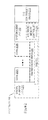
The following description and accompanying drawings are used to illustrate embodiments of the invention. In the drawings:
In FIG. 1A , a processor pipeline 100 includes a fetch stage 102, a length decode stage 104, a decode stage 106, an allocation stage 108, a renaming stage 110, a scheduling (also known as a dispatch or issue) stage 112, a register read/memory read stage 114, an execute stage 116, a write back/memory write stage 118, an exception handling stage 122, and a commit stage 124.
The front end unit 130 includes a branch prediction unit 132 coupled to an instruction cache unit 134, which is coupled to an instruction translation lookaside buffer (TLB) 136, which is coupled to an instruction fetch unit 138, which is coupled to a decode unit 140. The decode unit 140 (or decoder) may decode instructions, and generate as an output one or more micro-operations, micro-code entry points, microinstructions, other instructions, or other control signals, which are decoded from, or which otherwise reflect, or are derived from, the original instructions. The decode unit 140 may be implemented using various different mechanisms. Examples of suitable mechanisms include, but are not limited to, look-up tables, hardware implementations, programmable logic arrays (PLAs), microcode read only memories (ROMs), etc. In one embodiment, the core 190 includes a microcode ROM or other medium that stores microcode for certain macroinstructions (e.g., in decode unit 140 or otherwise within the front end unit 130). The decode unit 140 is coupled to a rename/allocator unit 152 in the execution engine unit 150.
The execution engine unit 150 includes the rename/allocator unit 152 coupled to a retirement unit 154 and a set of one or more scheduler unit(s) 156. The scheduler unit(s) 156 represents any number of different schedulers, including reservations stations, central instruction window, etc. The scheduler unit(s) 156 is coupled to the physical register file(s) unit(s) 158.
Each of the physical register file(s) units 158 represents one or more physical register files, different ones of which store one or more different data types, such as scalar integer, scalar floating point, packed integer, packed floating point, vector integer, vector floating point, status (e.g., an instruction pointer that is the address of the next instruction to be executed), etc. In one embodiment, the physical register file(s) unit 158 comprises a vector registers unit, a write mask registers unit, and a scalar registers unit. These register units may provide architectural vector registers, vector mask registers, and general purpose registers. The physical register file(s) unit(s) 158 is overlapped by the retirement unit 154 to illustrate various ways in which register renaming and out-of-order execution may be implemented (e.g., using a reorder buffer(s) and a retirement register file(s); using a future file(s), a history buffer(s), and a retirement register file(s); using a register maps and a pool of registers; etc.). The retirement unit 154 and the physical register file(s) unit(s) 158 are coupled to the execution cluster(s) 160. The execution cluster(s) 160 includes a set of one or more execution units 162 and a set of one or more memory access units 164. The execution units 162 may perform various operations (e.g., shifts, addition, subtraction, multiplication) and on various types of data (e.g., scalar floating point, packed integer, packed floating point, vector integer, vector floating point). While some embodiments may include a number of execution units dedicated to specific functions or sets of functions, other embodiments may include only one execution unit or multiple execution units that all perform all functions. The scheduler unit(s) 156, physical register file(s) unit(s) 158, and execution cluster(s) 160 are shown as being possibly plural because certain embodiments create separate pipelines for certain types of data/operations (e.g., a scalar integer pipeline, a scalar floating point/packed integer/packed floating point/vector integer/vector floating point pipeline, and/or a memory access pipeline that each have their own scheduler unit, physical register file(s) unit, and/or execution cluster—and in the case of a separate memory access pipeline, certain embodiments are implemented in which only the execution cluster of this pipeline has the memory access unit(s) 164). It should also be understood that where separate pipelines are used, one or more of these pipelines may be out-of-order issue/execution and the rest in-order.
The set of memory access units 164 is coupled to the memory unit 170, which includes a data TLB unit 172 coupled to a data cache unit 174 coupled to a level 2 (L2) cache unit 176. In one exemplary embodiment, the memory access units 164 may include a load unit, a store address unit, and a store data unit, each of which is coupled to the data TLB unit 172 in the memory unit 170. The instruction cache unit 134 is further coupled to a level 2 (L2) cache unit 176 in the memory unit 170. The L2 cache unit 176 is coupled to one or more other levels of cache and eventually to a main memory.
By way of example, the exemplary register renaming, out-of-order issue/execution core architecture may implement the pipeline 100 as follows: 1) the instruction fetch 138 performs the fetch and length decoding stages 102 and 104; 2) the decode unit 140 performs the decode stage 106; 3) the rename/allocator unit 152 performs the allocation stage 108 and renaming stage 110; 4) the scheduler unit(s) 156 performs the schedule stage 112; 5) the physical register file(s) unit(s) 158 and the memory unit 170 perform the register read/memory read stage 114; the execution cluster 160 perform the execute stage 116; 6) the memory unit 170 and the physical register file(s) unit(s) 158 perform the write back/memory write stage 118; 7) various units may be involved in the exception handling stage 122; and 8) the retirement unit 154 and the physical register file(s) unit(s) 158 perform the commit stage 124.
The core 190 may support one or more instructions sets (e.g., the x86 instruction set (with some extensions that have been added with newer versions); the MIPS instruction set of MIPS Technologies of Sunnyvale, Calif.; the ARM instruction set (with optional additional extensions such as NEON) of ARM Holdings of Sunnyvale, Calif.), including the instruction(s) described herein. In one embodiment, the core 190 includes logic to support a packed data instruction set extension (e.g., AVX1, AVX2, and/or some form of the generic vector friendly instruction format (U=0 and/or U=1), described below), thereby allowing the operations used by many multimedia applications to be performed using packed data.
It should be understood that the core may support multithreading (executing two or more parallel sets of operations or threads), and may do so in a variety of ways including time sliced multithreading, simultaneous multithreading (where a single physical core provides a logical core for each of the threads that physical core is simultaneously multithreading), or a combination thereof (e.g., time sliced fetching and decoding and simultaneous multithreading thereafter such as in the Intel® Hyperthreading technology).
While register renaming is described in the context of out-of-order execution, it should be understood that register renaming may be used in an in-order architecture. While the illustrated embodiment of the processor also includes separate instruction and data cache units 134/174 and a shared L2 cache unit 176, alternative embodiments may have a single internal cache for both instructions and data, such as, for example, a Level 1 (L1) internal cache, or multiple levels of internal cache. In some embodiments, the system may include a combination of an internal cache and an external cache that is external to the core and/or the processor. Alternatively, all of the cache may be external to the core and/or the processor.
Thus, different implementations of the processor 200 may include: 1) a CPU with the special purpose logic 208 being integrated graphics and/or scientific (throughput) logic (which may include one or more cores), and the cores 202A-N being one or more general purpose cores (e.g., general purpose in-order cores, general purpose out-of-order cores, a combination of the two); 2) a coprocessor with the cores 202A-N being a large number of special purpose cores intended primarily for graphics and/or scientific (throughput); and 3) a coprocessor with the cores 202A-N being a large number of general purpose in-order cores. Thus, the processor 200 may be a general-purpose processor, coprocessor or special-purpose processor, such as, for example, a network or communication processor, compression engine, graphics processor, GPGPU (general purpose graphics processing unit), a high-throughput many integrated core (MIC) coprocessor (including 30 or more cores), embedded processor, or the like. The processor may be implemented on one or more chips. The processor 200 may be a part of and/or may be implemented on one or more substrates using any of a number of process technologies, such as, for example, BiCMOS, CMOS, or NMOS.
The memory hierarchy includes one or more levels of cache within the cores, a set or one or more shared cache units 206, and external memory (not shown) coupled to the set of integrated memory controller units 214. The set of shared cache units 206 may include one or more mid-level caches, such as level 2 (L2), level 3 (L3), level 4 (L4), or other levels of cache, a last level cache (LLC), and/or combinations thereof. While in one embodiment a ring based interconnect unit 212 interconnects the special purpose logic 208, the set of shared cache units 206, and the system agent unit 210/integrated memory controller unit(s) 214, alternative embodiments may use any number of well-known techniques for interconnecting such units. In one embodiment, coherency is maintained between one or more cache units 206 and cores 202-A-N.
In some embodiments, one or more of the cores 202A-N are capable of multi-threading. The system agent 210 includes those components coordinating and operating cores 202A-N. The system agent unit 210 may include for example a power control unit (PCU) and a display unit. The PCU may be or include logic and components needed for regulating the power state of the cores 202A-N and the special purpose logic 208. The display unit is for driving one or more externally connected displays.
The cores 202A-N may be homogenous or heterogeneous in terms of architecture instruction set; that is, two or more of the cores 202A-N may be capable of execution the same instruction set, while others may be capable of executing only a subset of that instruction set or a different instruction set.
Referring now to FIG. 3 , shown is a block diagram of a system 300 in accordance with one embodiment of the present invention. The system 300 may include one or more processors 310, 315, which are coupled to a controller hub 320. In one embodiment the controller hub 320 includes a graphics memory controller hub (GMCH) 390 and an Input/Output Hub (IOH) 350 (which may be on separate chips); the GMCH 390 includes memory and graphics controllers to which are coupled memory 340 and a coprocessor 345; the IOH 350 is couples input/output (I/O) devices 360 to the GMCH 390. Alternatively, one or both of the memory and graphics controllers are integrated within the processor (as described herein), the memory 340 and the coprocessor 345 are coupled directly to the processor 310, and the controller hub 320 in a single chip with the IOH 350.
The optional nature of additional processors 315 is denoted in FIG. 3 with broken lines. Each processor 310, 315 may include one or more of the processing cores described herein and may be some version of the processor 200.
The memory 340 may be, for example, dynamic random access memory (DRAM), phase change memory (PCM), or a combination of the two. For at least one embodiment, the controller hub 320 communicates with the processor(s) 310, 315 via a multi-drop bus, such as a frontside bus (FSB), point-to-point interface such as QuickPath Interconnect (QPI), or similar connection 395.
In one embodiment, the coprocessor 345 is a special-purpose processor, such as, for example, a high-throughput MIC processor, a network or communication processor, compression engine, graphics processor, GPGPU, embedded processor, or the like. In one embodiment, controller hub 320 may include an integrated graphics accelerator.
There can be a variety of differences between the processors 310, 315 in terms of a spectrum of metrics of merit including architectural, microarchitectural, thermal, power consumption characteristics, and the like.
In one embodiment, the processor 310 executes instructions that control data processing operations of a general type. Embedded within the instructions may be coprocessor instructions. The processor 310 recognizes these coprocessor instructions as being of a type that should be executed by the attached coprocessor 345. Accordingly, the processor 310 issues these coprocessor instructions (or control signals representing coprocessor instructions) on a coprocessor bus or other interconnect, to coprocessor 345. Coprocessor(s) 345 accept and execute the received coprocessor instructions.
Referring now to FIG. 4 , shown is a block diagram of a first more specific exemplary system 400 in accordance with an embodiment of the present invention. As shown in FIG. 4 , multiprocessor system 400 is a point-to-point interconnect system, and includes a first processor 470 and a second processor 480 coupled via a point-to-point interconnect 450. Each of processors 470 and 480 may be some version of the processor 200. In one embodiment of the invention, processors 470 and 480 are respectively processors 310 and 315, while coprocessor 438 is coprocessor 345. In another embodiment, processors 470 and 480 are respectively processor 310 coprocessor 345.
A shared cache (not shown) may be included in either processor or outside of both processors, yet connected with the processors via P-P interconnect, such that either or both processors' local cache information may be stored in the shared cache if a processor is placed into a low power mode.
As shown in FIG. 4 , various I/O devices 414 may be coupled to first bus 416, along with a bus bridge 418 which couples first bus 416 to a second bus 420. In one embodiment, one or more additional processor(s) 415, such as coprocessors, high-throughput MIC processors, GPGPU's, accelerators (such as, e.g., graphics accelerators or digital signal processing (DSP) units), field programmable gate arrays, or any other processor, are coupled to first bus 416. In one embodiment, second bus 420 may be a low pin count (LPC) bus. Various devices may be coupled to a second bus 420 including, for example, a keyboard and/or mouse 422, communication devices 427 and a storage unit 428 such as a disk drive or other mass storage device which may include instructions/code and data 430, in one embodiment. Further, an audio I/O 424 may be coupled to the second bus 420. Note that other architectures are possible. For example, instead of the point-to-point architecture of FIG. 4 , a system may implement a multi-drop bus or other such architecture.
Referring now to FIG. 5 , shown is a block diagram of a second more specific exemplary system 500 in accordance with an embodiment of the present invention. Like elements in FIGS. 4 and 5 bear like reference numerals, and certain aspects of FIG. 4 have been omitted from FIG. 5 in order to avoid obscuring other aspects of FIG. 5 .
Referring now to FIG. 6 , shown is a block diagram of a SoC 600 in accordance with an embodiment of the present invention. Similar elements in FIG. 2 bear like reference numerals. Also, dashed lined boxes are optional features on more advanced SoCs. In FIG. 6 , an interconnect unit(s) 602 is coupled to: an application processor 610 which includes a set of one or more cores 202A-N and shared cache unit(s) 206; a system agent unit 210; a bus controller unit(s) 216; an integrated memory controller unit(s) 214; a set or one or more coprocessors 620 which may include integrated graphics logic, an image processor, an audio processor, and a video processor; an static random access memory (SRAM) unit 630; a direct memory access (DMA) unit 632; and a display unit 640 for coupling to one or more external displays. In one embodiment, the coprocessor(s) 620 include a special-purpose processor, such as, for example, a network or communication processor, compression engine, GPGPU, a high-throughput MIC processor, embedded processor, or the like.
Embodiments of the mechanisms disclosed herein may be implemented in hardware, software, firmware, or a combination of such implementation approaches. Embodiments of the invention may be implemented as computer programs or program code executing on programmable systems comprising at least one processor, a storage system (including volatile and non-volatile memory and/or storage elements), at least one input device, and at least one output device.
Program code, such as code within code and data 430 illustrated in FIG. 4 , may be applied to input instructions to perform the functions described herein and generate output information. The output information may be applied to one or more output devices, in known fashion. For purposes of this application, a processing system includes any system that has a processor, such as, for example; a digital signal processor (DSP), a microcontroller, an application specific integrated circuit (ASIC), or a microprocessor.
The program code may be implemented in a high level procedural or object oriented programming language to communicate with a processing system. The program code may also be implemented in assembly or machine language, if desired. In fact, the mechanisms described herein are not limited in scope to any particular programming language. In any case, the language may be a compiled or interpreted language.
One or more aspects of at least one embodiment may be implemented by representative instructions stored on a machine-readable medium which represents various logic within the processor, which when read by a machine causes the machine to fabricate logic to perform the techniques described herein. Such representations, known as “IP cores” may be stored on a tangible, machine readable medium and supplied to various customers or manufacturing facilities to load into the fabrication machines that actually make the logic or processor.
Such machine-readable storage media may include, without limitation, non-transitory, tangible arrangements of articles manufactured or formed by a machine or device, including storage media such as hard disks, any other type of disk including floppy disks, optical disks, compact disk read-only memories (CD-ROMs), compact disk rewritable's (CD-RWs), and magneto-optical disks, semiconductor devices such as read-only memories (ROMs), random access memories (RAMs) such as dynamic random access memories (DRAMs), static random access memories (SRAMs), erasable programmable read-only memories (EPROMs), flash memories, electrically erasable programmable read-only memories (EEPROMs), phase change memory (PCM), magnetic or optical cards, or any other type of media suitable for storing electronic instructions.
Accordingly, embodiments of the invention also include non-transitory, tangible machine-readable media containing instructions or containing design data, such as Hardware Description Language (HDL), which defines structures, circuits, apparatuses, processors and/or system features described herein. Such embodiments may also be referred to as program products.
In some cases, an instruction converter may be used to convert an instruction from a source instruction set to a target instruction set. For example, the instruction converter may translate (e.g., using static binary translation, dynamic binary translation including dynamic compilation), morph, emulate, or otherwise convert an instruction to one or more other instructions to be processed by the core. The instruction converter may be implemented in software, hardware, firmware, or a combination thereof. The instruction converter may be on processor, off processor, or part on and part off processor.
Similarly, FIG. 7 shows the program in the high level language 702 may be compiled using an alternative instruction set compiler 708 to generate alternative instruction set binary code 710 that may be natively executed by a processor without at least one x86 instruction set core 714—(e.g., a processor with cores that execute the MIPS instruction set of MIPS Technologies of Sunnyvale, Calif. and/or that execute the ARM instruction set of ARM Holdings of Sunnyvale, Calif.). The instruction converter 712 is used to convert the x86 binary code 706 into code that may be natively executed by the processor without an x86 instruction set core 714. This converted code is not likely to be the same as the alternative instruction set binary code 710 because an instruction converter capable of this is difficult to make; however, the converted code will accomplish the general operation and be made up of instructions from the alternative instruction set. Thus, the instruction converter 712 represents software, firmware, hardware, or a combination thereof that, through emulation, simulation or any other process, allows a processor or other electronic device that does not have an x86 instruction set processor or core to execute the x86 binary code 706.
The embodiments of the invention described below include a set of SIMD/vector instructions allowing the expression of a value to propagate from iterations in which a variable is defined to those following it in which the variable may not be defined or may be used before it is defined. These embodiments enable the compiler to perform array expansion of scalars as required to vectorize the loop. In the example below the compiler cannot vectorize this loop since the compiler has no good way to express the data dependence between variable z and array B in SIMD ISA:
| z = 18; | ||
| for (int i = 0; i<N; i++) { | ||
| if (A[i] > 0) { | ||
| z = A[i]; | ||
| } | ||
| B[i] = z; | ||
| } | ||
If N=8 and A[i] contains {0, 11, 12, 0, 0, 15, 16, 0} the predicate mask representing the condition (A[i]>0) would be {0, 1, 1, 0, 0, 1, 1, 0} and after executing the loop, B should contain {18, 11, 12, 12, 12, 15, 16, 16}. Note that when the predicate is 0, z and B [i] contain the value of z from the previous iteration, and until the first SIMD element in which the predicate is 1 they contain the scalar value on entry to the SIMD iteration. Note that the vector version of z or the vector B can be computed as a permutation of elements of two vectors; vector A and a vector initialized with the scalar value of z live on entry to the SIMD iteration. Assuming a SIMD vector length of 8 for the example above, the permutation index vector would be {8, 1, 2, 2, 2, 5, 6, 6} where index values 0 through 7 select an element of A and
Since some instruction sets (e.g., such as the advanced vector extensions (AVX) designed by the assignee of the present application) include permutation instructions to permute elements from one or two AVX registers to a destination AVX register, all that is needed is a way to compute index values from an input predicate mask. This will enable the compiler to express the permutation represented in this example code.
The embodiments of the invention described below include three SIMD instructions that take an input mask register and generate an index vector. These instructions can be used by the compiler to vectorize loops such as the example provided above as well as other loops with loop carried dependences. In one embodiment, the new instructions have the following formats:
vPropagateTrueIndex[BWDQ] v1, k2, imm1
vPropagateFalseIndex[BWDQ] v1, k2
vPropagateShiftTrue[BWDQ] v1, k2
and embodiments of each are described in detail below.
(1) vPropagateTrueIndex[BWDQ] v1, k2, imm1:
This instruction generates byte/word/dword/qword element indices in v1 by propagating the element index of the last TRUE bit found in a least significant to most significant bit traversal of the mask. With an immediate value of 0, until the first TRUE bit is found the bit position is simply recorded in v1. Thereafter for each FALSE bit observed in k2 the index of the last TRUE bit is added to the vector length and recorded. For an immediate value of 1, the vector length is added to the element index prior to recording at positions corresponding to TRUE bits in k2. In one embodiment, the destination register of this instruction is used as a permutation index in the instruction that permutes elements from two vectors.
Pseudo-code describing an implementation of one embodiment of the invention is as follows:
| vPropagateTrueIndex(v1, k2, imm1) { |
| int j, lastTruePos; |
| Bit trueSeen = FALSE; |
| for (j=0; j<VLEN; j++) { // VLEN is 8 for Q, 16 for D and 32 |
| for W |
| if (k2[j]) { |
| lastTruePos = j + VLEN; |
| trueSeen = TRUE; |
| if (imm1[0:0]) { |
| v[j] = lastTruePos; |
| else { |
| v1[j] = j; |
| } |
| } |
| else { // FALSE bit in k2 |
| if (trueSeen) { |
| v1[j] = lastTruePos; |
| } |
| else { |
| v1[j] = j; |
| } |
| } |
| } |
| } |
Two specific examples are shown in FIG. 8 . For the first example, with an immediate value of 0, until the first FALSE bit following a TRUE bit, the current bit position is simply recorded in v1. For all FALSE bits following the initial two TRUE bits, the index of the last TRUE bit is added to the vector length and recorded. Thus, at bit position 4, the index of the last true bit (3) is added to the vector length (16), resulting in an output value of 19; at bit position 6, the index of the last true bit (5) is added to the vector length (16), resulting in an output value of 21; at bit positions 8-13, the index of the last true bit (7) is added to the vector length (16) resulting in an output value of 23, as illustrated.
For the example provided with an immediate value of 1, for each TRUE bit in the input mask (K2), the output is set equal to the sum of the current bit position and the vector length. For example, the output for bit position 2 is set equal to 2+16=18; the output for bit position 3 is set equal to 3+16=19; the output for bit position 5 is set equal to 5+16=21; output for bit position 7 is set equal to 7+16=23; the output for bit position 14 is set equal to 14+16=30; and the output for bit position 15 is set equal to 15+16=31. For each FALSE value following the first TRUE value in the input mask, the value of the last output value is repeated as the output.
The above instruction enables the compiler to handle a loop carried dependence between a conditionally computed value and a potential use of that value in the same or a subsequent iteration, or if the value is live out of the loop.
(2) vPropagateFalseIndex[BWDQ] v1, k2:
This instruction generates byte/word/dword element indices in v1 by propagating the element index of the last FALSE bit found in a least significant bit to most significant bit traversal of the mask. The value (VLEN-1) (where VLEN is the vector length) is propagated as the element index until the first FALSE bit is encountered. The destination register of this instruction can be used as a permutation index in the instruction that permutes the elements of a vector.
The Pseudo Code for one embodiment is as follows:
| vPropagateFalseIndex(v1, k2) { |
| int j, |
| int lastFalsePos = VLEN−1; // VLEN is 8 for Q, 16 for D and |
| 32 for W |
| for (j=0; j<VLEN; j++) { |
| if (k2[j]) { |
| v1[j] = lastFalsePos; |
| } |
| else { |
| v1[j] = j; |
| lastFalsePos = j; |
| } |
| } |
| } |
In the example provided in
In one embodiment, this instruction is used to propagate a conditionally computed value across multiple SIMD iterations.
(3) vPropagateShiftTrueIndex[BWDQ] v1, k0:
This instruction traverses vector mask elements from element 0 to the element VL−1 where VL is the vector length, and records the element position of the last true element in k0 in the next corresponding element in v1. Until the first true bit is seen in k0, VL is recorded in the corresponding next element in v1. VL is always recorded in the first element of v1. In one embodiment, the output of this instruction is used as a permutation index in the instruction that permutes elements from two vectors.
This instruction enables the compiler to handle a loop carried dependence between a conditionally or unconditionally computed value and a potential use of that value in the next or a subsequent iteration. An exemplary loop is as follows:
| lastZ = 1; | ||
| for (int i = 0; i<N; i++) { | ||
| z = A[i]/i; | ||
| if (z != lastZ) { | ||
| B[i] = z; | ||
| } | ||
| lastZ = z; | ||
| } | ||
In the example provided in FIG. 10 , the vector length (16) is recorded until bit position 3 at which point, and thereafter, the value of the element position of the last true element in k0 is output (starting with an output value of 2 corresponding to the bit position of the last TRUE value in the input mask).
The embodiments of the invention described herein allow compilers to vectorize loops containing one or more scalar (with respect to the loop index variable) definitions that do not dominate all uses within the loop, thereby improving performance. By adding new instructions to compute index vectors from predicate masks, the present invention enables the compiler to vectorize loops such as the ones described above by expressing vector element permutations that represent certain loop-carried dependences. Thus the embodiments of the invention have the potential of yielding significant improvement in single thread performance on certain applications and system software.
Exemplary Instruction Formats
Embodiments of the instruction(s) described herein may be embodied in different formats. Additionally, exemplary systems, architectures, and pipelines are detailed below. Embodiments of the instruction(s) may be executed on such systems, architectures, and pipelines, but are not limited to those detailed.
A vector friendly instruction format is an instruction format that is suited for vector instructions (e.g., there are certain fields specific to vector operations). While embodiments are described in which both vector and scalar operations are supported through the vector friendly instruction format, alternative embodiments use only vector operations the vector friendly instruction format.
While embodiments of the invention will be described in which the vector friendly instruction format supports the following: a 64 byte vector operand length (or size) with 32 bit (4 byte) or 64 bit (8 byte) data element widths (or sizes) (and thus, a 64 byte vector consists of either 16 doubleword-size elements or alternatively, 8 quadword-size elements); a 64 byte vector operand length (or size) with 16 bit (2 byte) or 8 bit (1 byte) data element widths (or sizes); a 32 byte vector operand length (or size) with 32 bit (4 byte), 64 bit (8 byte), 16 bit (2 byte), or 8 bit (1 byte) data element widths (or sizes); and a 16 byte vector operand length (or size) with 32 bit (4 byte), 64 bit (8 byte), 16 bit (2 byte), or 8 bit (1 byte) data element widths (or sizes); alternative embodiments may support more, less and/or different vector operand sizes (e.g., 256 byte vector operands) with more, less, or different data element widths (e.g., 128 bit (16 byte) data element widths).
The class A instruction templates in FIG. 11A include: 1) within the no memory access 1105 instruction templates there is shown a no memory access, full round control type operation 1110 instruction template and a no memory access, data transform type operation 1115 instruction template; and 2) within the memory access 1120 instruction templates there is shown a memory access, temporal 1125 instruction template and a memory access, non-temporal 1130 instruction template. The class B instruction templates in FIG. 11B include: 1) within the no memory access 1105 instruction templates there is shown a no memory access, write mask control, partial round control type operation 1112 instruction template and a no memory access, write mask control, vsize type operation 1117 instruction template; and 2) within the memory access 1120 instruction templates there is shown a memory access, write mask control 1127 instruction template.
The generic vector friendly instruction format 1100 includes the following fields listed below in the order illustrated in FIGS. 11A-11B .
Data element width field 1164—its content distinguishes which one of a number of data element widths is to be used (in some embodiments for all instructions; in other embodiments for only some of the instructions). This field is optional in the sense that it is not needed if only one data element width is supported and/or data element widths are supported using some aspect of the opcodes.
Write mask field 1170—its content controls, on a per data element position basis, whether that data element position in the destination vector operand reflects the result of the base operation and augmentation operation. Class A instruction templates support merging-writemasking, while class B instruction templates support both merging- and zeroing-writemasking. When merging, vector masks allow any set of elements in the destination to be protected from updates during the execution of any operation (specified by the base operation and the augmentation operation); in other one embodiment, preserving the old value of each element of the destination where the corresponding mask bit has a 0. In contrast, when zeroing vector masks allow any set of elements in the destination to be zeroed during the execution of any operation (specified by the base operation and the augmentation operation); in one embodiment, an element of the destination is set to 0 when the corresponding mask bit has a 0 value. A subset of this functionality is the ability to control the vector length of the operation being performed (that is, the span of elements being modified, from the first to the last one); however, it is not necessary that the elements that are modified be consecutive. Thus, the write mask field 1170 allows for partial vector operations, including loads, stores, arithmetic, logical, etc. While embodiments of the invention are described in which the write mask field's 1170 content selects one of a number of write mask registers that contains the write mask to be used (and thus the write mask field's 1170 content indirectly identifies that masking to be performed), alternative embodiments instead or additional allow the mask write field's 1170 content to directly specify the masking to be performed.
Instruction Templates of Class A
In the case of the non-memory access 1105 instruction templates of class A, the alpha field 1152 is interpreted as an RS field 1152A, whose content distinguishes which one of the different augmentation operation types are to be performed (e.g., round 1152A.1 and data transform 1152A.2 are respectively specified for the no memory access, round type operation 1110 and the no memory access, data transform type operation 1115 instruction templates), while the beta field 1154 distinguishes which of the operations of the specified type is to be performed. In the no memory access 1105 instruction templates, the scale field 1160, the displacement field 1162A, and the displacement scale filed 1162B are not present.
No-Memory Access Instruction Templates—Full Round Control Type Operation
In the no memory access full round control type operation 1110 instruction template, the beta field 1154 is interpreted as a round control field 1154A, whose content(s) provide static rounding. While in the described embodiments of the invention the round control field 1154A includes a suppress all floating point exceptions (SAE) field 1156 and a round operation control field 1158, alternative embodiments may support may encode both these concepts into the same field or only have one or the other of these concepts/fields (e.g., may have only the round operation control field 1158).
Round operation control field 1158—its content distinguishes which one of a group of rounding operations to perform (e.g., Round-up, Round-down, Round-towards-zero and Round-to-nearest). Thus, the round operation control field 1158 allows for the changing of the rounding mode on a per instruction basis. In one embodiment of the invention where a processor includes a control register for specifying rounding modes, the round operation control field's 1158 content overrides that register value.
No Memory Access Instruction Templates—Data Transform Type Operation
In the no memory access data transform type operation 1115 instruction template, the beta field 1154 is interpreted as a data transform field 1154B, whose content distinguishes which one of a number of data transforms is to be performed (e.g., no data transform, swizzle, broadcast).
In the case of a memory access 1120 instruction template of class A, the alpha field 1152 is interpreted as an eviction hint field 1152B, whose content distinguishes which one of the eviction hints is to be used (in FIG. 11A , temporal 1152B.1 and non-temporal 1152B.2 are respectively specified for the memory access, temporal 1125 instruction template and the memory access, non-temporal 1130 instruction template), while the beta field 1154 is interpreted as a data manipulation field 1154C, whose content distinguishes which one of a number of data manipulation operations (also known as primitives) is to be performed (e.g., no manipulation; broadcast; up conversion of a source; and down conversion of a destination). The memory access 1120 instruction templates include the scale field 1160, and optionally the displacement field 1162A or the displacement scale field 1162B.
Vector memory instructions perform vector loads from and vector stores to memory, with conversion support. As with regular vector instructions, vector memory instructions transfer data from/to memory in a data element-wise fashion, with the elements that are actually transferred is dictated by the contents of the vector mask that is selected as the write mask.
Memory Access Instruction Templates—Temporal
Temporal data is data likely to be reused soon enough to benefit from caching. This is, however, a hint, and different processors may implement it in different ways, including ignoring the hint entirely.
Memory Access Instruction Templates—Non-Temporal
Non-temporal data is data unlikely to be reused soon enough to benefit from caching in the 1st-level cache and should be given priority for eviction. This is, however, a hint, and different processors may implement it in different ways, including ignoring the hint entirely.
Instruction Templates of Class B
In the case of the instruction templates of class B, the alpha field 1152 is interpreted as a write mask control (Z) field 1152C, whose content distinguishes whether the write masking controlled by the write mask field 1170 should be a merging or a zeroing.
In the case of the non-memory access 1105 instruction templates of class B, part of the beta field 1154 is interpreted as an RL field 1157A, whose content distinguishes which one of the different augmentation operation types are to be performed (e.g., round 1157A.1 and vector length (VSIZE) 1157A.2 are respectively specified for the no memory access, write mask control, partial round control type operation 1112 instruction template and the no memory access, write mask control, VSIZE type operation 1117 instruction template), while the rest of the beta field 1154 distinguishes which of the operations of the specified type is to be performed. In the no memory access 1105 instruction templates, the scale field 1160, the displacement field 1162A, and the displacement scale filed 1162B are not present.
In the no memory access, write mask control, partial round control type operation 1110 instruction template, the rest of the beta field 1154 is interpreted as a round operation field 1159A and exception event reporting is disabled (a given instruction does not report any kind of floating-point exception flag and does not raise any floating point exception handler).
Round operation control field 1159A—just as round operation control field 1158, its content distinguishes which one of a group of rounding operations to perform (e.g., Round-up, Round-down, Round-towards-zero and Round-to-nearest). Thus, the round operation control field 1159A allows for the changing of the rounding mode on a per instruction basis. In one embodiment of the invention where a processor includes a control register for specifying rounding modes, the round operation control field's 1158 content overrides that register value.
In the no memory access, write mask control, VSIZE type operation 1117 instruction template, the rest of the beta field 1154 is interpreted as a vector length field 1159B, whose content distinguishes which one of a number of data vector lengths is to be performed on (e.g., 128, 256, or 512 byte).
In the case of a memory access 1120 instruction template of class B, part of the beta field 1154 is interpreted as a broadcast field 1157B, whose content distinguishes whether or not the broadcast type data manipulation operation is to be performed, while the rest of the beta field 1154 is interpreted the vector length field 1159B. The memory access 1120 instruction templates include the scale field 1160, and optionally the displacement field 1162A or the displacement scale field 1162B.
With regard to the generic vector friendly instruction format 1100, a full opcode field 1174 is shown including the format field 1140, the base operation field 1142, and the data element width field 1164. While one embodiment is shown where the full opcode field 1174 includes all of these fields, the full opcode field 1174 includes less than all of these fields in embodiments that do not support all of them. The full opcode field 1174 provides the operation code (opcode).
The augmentation operation field 1150, the data element width field 1164, and the write mask field 1170 allow these features to be specified on a per instruction basis in the generic vector friendly instruction format.
The combination of write mask field and data element width field create typed instructions in that they allow the mask to be applied based on different data element widths.
The various instruction templates found within class A and class B are beneficial in different situations. In some embodiments of the invention, different processors or different cores within a processor may support only class A, only class B, or both classes. For instance, a high performance general purpose out-of-order core intended for general-purpose computing may support only class B, a core intended primarily for graphics and/or scientific (throughput) computing may support only class A, and a core intended for both may support both (of course, a core that has some mix of templates and instructions from both classes but not all templates and instructions from both classes is within the purview of the invention). Also, a single processor may include multiple cores, all of which support the same class or in which different cores support different class. For instance, in a processor with separate graphics and general purpose cores, one of the graphics cores intended primarily for graphics and/or scientific computing may support only class A, while one or more of the general purpose cores may be high performance general purpose cores with out of order execution and register renaming intended for general-purpose computing that support only class B. Another processor that does not have a separate graphics core, may include one more general purpose in-order or out-of-order cores that support both class A and class B. Of course, features from one class may also be implemented in the other class in different embodiments of the invention. Programs written in a high level language would be put (e.g., just in time compiled or statically compiled) into an variety of different executable forms, including: 1) a form having only instructions of the class(es) supported by the target processor for execution; or 2) a form having alternative routines written using different combinations of the instructions of all classes and having control flow code that selects the routines to execute based on the instructions supported by the processor which is currently executing the code.
It should be understood that, although embodiments of the invention are described with reference to the specific vector friendly instruction format 1200 in the context of the generic vector friendly instruction format 1100 for illustrative purposes, the invention is not limited to the specific vector friendly instruction format 1200 except where claimed. For example, the generic vector friendly instruction format 1100 contemplates a variety of possible sizes for the various fields, while the specific vector friendly instruction format 1200 is shown as having fields of specific sizes. By way of specific example, while the data element width field 1164 is illustrated as a one bit field in the specific vector friendly instruction format 1200, the invention is not so limited (that is, the generic vector friendly instruction format 1100 contemplates other sizes of the data element width field 1164).
The generic vector friendly instruction format 1100 includes the following fields listed below in the order illustrated in FIG. 12A .
EVEX Prefix (Bytes 0-3) 1202—is encoded in a four-byte form.
Format Field 1140 (EVEX Byte 0, bits [7:0])—the first byte (EVEX Byte 0) is the format field 1140 and it contains 0x62 (the unique value used for distinguishing the vector friendly instruction format in one embodiment of the invention).
The second-fourth bytes (EVEX Bytes 1-3) include a number of bit fields providing specific capability.
REX field 1205 (EVEX Byte 1, bits [7-5])—consists of a EVEX.R bit field (EVEX Byte 1, bit [7]—R), EVEX.X bit field (EVEX byte 1, bit [6]—X), and 1157 BEX byte 1, bit[5]—B). The EVEX.R, EVEX.X, and EVEX.B bit fields provide the same functionality as the corresponding VEX bit fields, and are encoded using 1s complement form, i.e. ZMM0 is encoded as 1111B, ZMM15 is encoded as 0000B. Other fields of the instructions encode the lower three bits of the register indexes as is known in the art (rrr, xxx, and bbb), so that Rrrr, Xxxx, and Bbbb may be formed by adding EVEX.R, EVEX.X, and EVEX.B.
Opcode map field 1215 (EVEX byte 1, bits [3:0]—mmmm)—its content encodes an implied leading opcode byte (0F, 0F 38, or 0F 3).
Data element width field 1164 (EVEX byte 2, bit [7]—W)—is represented by the notation EVEX.W. EVEX.W is used to define the granularity (size) of the datatype (either 32-bit data elements or 64-bit data elements).
EVEX.vvvv 1220 (EVEX Byte 2, bits [6:3]—vvvv)—the role of EVEX.vvvv may include the following: 1) EVEX.vvvv encodes the first source register operand, specified in inverted (1s complement) form and is valid for instructions with 2 or more source operands; 2) EVEX.vvvv encodes the destination register operand, specified in 1s complement form for certain vector shifts; or 3) EVEX.vvvv does not encode any operand, the field is reserved and should contain 1111b. Thus, EVEX.vvvv field 1220 encodes the 4 low-order bits of the first source register specifier stored in inverted (1s complement) form. Depending on the instruction, an extra different EVEX bit field is used to extend the specifier size to 32 registers.
Prefix encoding field 1225 (EVEX byte 2, bits [1:0]−pp)—provides additional bits for the base operation field. In addition to providing support for the legacy SSE instructions in the EVEX prefix format, this also has the benefit of compacting the SIMD prefix (rather than requiring a byte to express the SIMD prefix, the EVEX prefix requires only 2 bits). In one embodiment, to support legacy SSE instructions that use a SIMD prefix (66H, F2H, F3H) in both the legacy format and in the EVEX prefix format, these legacy SIMD prefixes are encoded into the SIMD prefix encoding field; and at runtime are expanded into the legacy SIMD prefix prior to being provided to the decoder's PLA (so the PLA can execute both the legacy and EVEX format of these legacy instructions without modification). Although newer instructions could use the EVEX prefix encoding field's content directly as an opcode extension, certain embodiments expand in a similar fashion for consistency but allow for different meanings to be specified by these legacy SIMD prefixes. An alternative embodiment may redesign the PLA to support the 2 bit SIMD prefix encodings, and thus not require the expansion.
Alpha field 1152 (EVEX byte 3, bit [7]—EH; also known as EVEX.EH, EVEX.rs, EVEX.RL, EVEX.write mask control, and EVEX.N; also illustrated with α)—as previously described, this field is context specific.
Beta field 1154 (EVEX byte 3, bits [6:4]—SSS, also known as EVEX.s2-0, EVEX.r2-0, EVEX.rr1, EVEX.LL0, EVEX.LLB; also illustrated with βββ)—as previously described, this field is context specific.
Write mask field 1170 (EVEX byte 3, bits [2:0]—kkk)—its content specifies the index of a register in the write mask registers as previously described. In one embodiment of the invention, the specific value EVEX.kkk=000 has a special behavior implying no write mask is used for the particular instruction (this may be implemented in a variety of ways including the use of a write mask hardwired to all ones or hardware that bypasses the masking hardware).
Real Opcode Field 1230 (Byte 4) is also known as the opcode byte. Part of the opcode is specified in this field.
MOD R/M Field 1240 (Byte 5) includes MOD field 1242, Reg field 1244, and R/M field 1246. As previously described, the MOD field's 1242 content distinguishes between memory access and non-memory access operations. The role of Reg field 1244 can be summarized to two situations: encoding either the destination register operand or a source register operand, or be treated as an opcode extension and not used to encode any instruction operand. The role of R/M field 1246 may include the following: encoding the instruction operand that references a memory address, or encoding either the destination register operand or a source register operand.
Scale, Index, Base (SIB) Byte (Byte 6)—As previously described, the scale field's 1250 content, including ss field 1252, is used for memory address generation. SIB.xxx 1254 and SIB.bbb 1256—the contents of these fields have been previously referred to with regard to the register indexes Xxxx and Bbbb.
Full Opcode Field
Register Index Field
Augmentation Operation Field
When U=1, the alpha field 1152 (EVEX byte 3, bit [7]—EH) is interpreted as the write mask control (Z) field 1152C. When U=1 and the MOD field 1242 contains 11 (signifying a no memory access operation), part of the beta field 1154 (EVEX byte 3, bit [4]—S0) is interpreted as the RL field 1157A; when it contains a 1 (round 1157A.1) the rest of the beta field 1154 (EVEX byte 3, bit [6-5]—S2-1) is interpreted as the round operation field 1159A, while when the RL field 1157A contains a 0 (VSIZE 1157.A2) the rest of the beta field 1154 (EVEX byte 3, bit [6-5]—S2-1) is interpreted as the vector length field 1159B (EVEX byte 3, bit [6-5]—L1-0). When U=1 and the MOD field 1242 contains 00, 01, or 10 (signifying a memory access operation), the beta field 1154 (EVEX byte 3, bits [6:4]—SSS) is interpreted as the vector length field 1159B (EVEX byte 3, bit [6-5]—L1-0) and the broadcast field 1157B (EVEX byte 3, bit [4]—B).
| Adjustable | |||
| Vector Length | Class | Operations | Registers |
| Instruction | A (FIG. 11A; | 1110, 1115, | zmm registers |
| Templates that | U = 0) | 1125, 1130 | (the vector |
| do not include | length is 64 byte) | ||
| the vector length | B (FIG. 11B; | 1112 | |
| field | |||
| 1159B | U = 1) | (the vector | |
| length is 64 byte) | |||
| Instruction | B (FIG. 11B; | 1117, 1127 | zmm, ymm, or |
| Templates that | U = 1) | xmm registers | |
| do include the | (the vector | ||
| vector length | length is 64 byte, | ||
| |
32 byte, or 16 | ||
| byte) depending | |||
| on the | |||
| length field | |||
| 1159B | |||
In other words, the vector length field 1159B selects between a maximum length and one or more other shorter lengths, where each such shorter length is half the length of the preceding length; and instructions templates without the vector length field 1159B operate on the maximum vector length. Further, in one embodiment, the class B instruction templates of the specific vector friendly instruction format 1200 operate on packed or scalar single/double-precision floating point data and packed or scalar integer data. Scalar operations are operations performed on the lowest order data element position in an zmm/ymm/xmm register; the higher order data element positions are either left the same as they were prior to the instruction or zeroed depending on the embodiment.
Write mask registers 1315—in the embodiment illustrated, there are 8 write mask registers (k0 through k7), each 64 bits in size. In an alternate embodiment, the write mask registers 1315 are 16 bits in size. As previously described, in one embodiment of the invention, the vector mask register k0 cannot be used as a write mask; when the encoding that would normally indicate k0 is used for a write mask, it selects a hardwired write mask of 0xFFFF, effectively disabling write masking for that instruction.
General-purpose registers 1325—in the embodiment illustrated, there are sixteen 64-bit general-purpose registers that are used along with the existing x86 addressing modes to address memory operands. These registers are referenced by the names RAX, RBX, RCX, RDX, RBP, RSI, RDI, RSP, and R8 through R15.
Scalar floating point stack register file (x87 stack) 1345, on which is aliased the MMX packed integer flat register file 1350—in the embodiment illustrated, the x87 stack is an eight-element stack used to perform scalar floating-point operations on 32/64/80-bit floating point data using the x87 instruction set extension; while the MMX registers are used to perform operations on 64-bit packed integer data, as well as to hold operands for some operations performed between the MMX and XMM registers.
Alternative embodiments of the invention may use wider or narrower registers. Additionally, alternative embodiments of the invention may use more, less, or different register files and registers.
The local subset of the L2 cache 1404 is part of a global L2 cache that is divided into separate local subsets, one per processor core. Each processor core has a direct access path to its own local subset of the L2 cache 1404. Data read by a processor core is stored in its L2 cache subset 1404 and can be accessed quickly, in parallel with other processor cores accessing their own local L2 cache subsets. Data written by a processor core is stored in its own L2 cache subset 1404 and is flushed from other subsets, if necessary. The ring network ensures coherency for shared data. The ring network is bi-directional to allow agents such as processor cores, L2 caches and other logic blocks to communicate with each other within the chip. Each ring data-path is 1012-bits wide per direction.
Claims (23)
1. A method for propagating conditionally evaluated values comprising operations of:
reading each value contained in an input mask register, each value being a true value or a false value and having a bit position associated therewith;
for each true value read from the input mask register, generating a first result containing the bit position of the true value;
for each false value read from the input mask register following a first true value in bit position, adding a vector length of the input mask register to a bit position of a last true value in bit position read from the input mask register to generate a second result; and
storing each of the first results and second results in bit positions, of an output register, corresponding to bit positions read from the input mask register.
2. The method as in claim 1 further comprising:
for each false value read from the input mask register prior to the first true value in bit position, generating a third result containing the bit position of the false value read from the input mask register prior to the first true value; and
storing each of the third results in bit positions, of the output register, corresponding to positions read from the input mask register.
3. The method as in claim 1 further comprising:
reading an immediate value and performing the operations only if the immediate value is set to a first value.
4. The method as in claim 3 wherein if the immediate value is not set to the first value then performing a second set of operations.
5. The method as in claim 4 wherein the second set of operations comprises:
reading each value contained in the input mask register, each value being a true value or a false value and having a bit position associated therewith;
for each true value read from the input mask register, generating a third result containing the bit position of the true value added to the vector length; and
storing each of the third results in bit positions, of the output register, corresponding to bit positions read from the input mask register.
6. The method as in claim 5 further comprising:
storing results of the third results to bit positions, of the output register, corresponding to bit positions read from the input mask register following the first true value in bit position that contain a false value.
7. The method as in claim 6 further comprising:
for each false value read from the input mask register prior to the first true value in bit position, storing the bit position of the false value read from the input mask register prior to the first true value in the output register in a corresponding bit position of the output register.
8. A processor to execute one or more instructions to perform operations of:
reading each value contained in an input mask register, each value being a true value or a false value and having a bit position associated therewith;
for each true value read from the input mask register, generating a first result containing the bit position of the true value;
for each false value read from the input mask register following a first true value in bit position, adding a vector length of the input mask register to a bit position of a last true value in bit position read from the input mask register to generate a second result; and
storing each of the first results and second results in bit positions, of an output register, corresponding to bit positions read from the input mask register.
9. The processor as in claim 8 to execute the one or more instructions to perform further operations of:
for each false value read from the input mask register prior to the first true value in bit position, generating a third result containing the bit position of the false value read from the input mask register prior to the first true value; and
storing each of the third results in bit positions, of the output register, corresponding to bit positions read from the input mask register.
10. The processor as in claim 8 to execute the one or more instructions to perform further operations of:
reading an immediate value and performing the operations only if the immediate value is set to a first value.
11. The processor as in claim 10 wherein if the immediate value is not set to the first value then the processor is to perform a second set of operations.
12. The processor as in claim 11 wherein the second set of operations comprises:
reading each value contained in the input mask register, each value being a true value or a false value and having a bit position associated therewith;
for each true value read from the input mask register, generating a third result containing the bit position of the true value added to the vector length; and
storing each of the third results in bit positions, of the output register, corresponding to bit positions read from the input mask register.
13. The processor as in claim 12 to execute the one or more instructions to perform further operations of:
storing results of the third results to bit positions, of the output register, corresponding to bit positions read from the input mask register following the first true value in bit position that contain a false value.
14. The processor as in claim 13 to execute the one or more instructions to perform further operations of:
for each false value read from the input mask register prior to the first true value in bit position, storing the bit position of the false value read from the input mask register prior to the first true value in the output register in a corresponding bit position of the output register.
15. A system comprising:
a memory for storing instructions and data;
a processor to execute one of the instructions to perform operations of:
reading each value contained in an input mask register, each value being a true value or a false value and having a bit position associated therewith;
for each true value read from the input mask register, generating a first result containing the bit position of the true value;
for each false value read from the input mask register following a first true value in bit position, adding a vector length of the input mask register to a bit position of a last true value in bit position read from the input mask register to generate a second result; and
storing each of the first results and second results in bit positions, of an output register, corresponding to bit positions read from the input mask register.
16. The system as in claim 15 wherein the processor is to execute the one instruction to perform further operations of:
for each false value read from the input mask register prior to the first true value in bit position, generating a third result containing the bit position of the false value read from the input mask register prior to the first true value; and
storing each of the third results in bit positions, of the output register, corresponding to bit positions read from the input mask register.
17. The system as in claim 15 wherein the processor is to execute the one instruction to perform further operations of:
reading an immediate value and performing the operations only if the immediate value is set to a first value.
18. The system as in claim 17 wherein if the immediate value is not set to the first value then the processor is to perform a second set of operations.
19. The system as in claim 18 wherein the second set of operations comprises:
reading each value contained in the input mask register, each value being a true value or a false value and having a bit position associated therewith;
for each true value read from the input mask register, generating a third result containing the bit position of the true value added to the vector length; and
storing each of the third results in bit positions, of the output register, corresponding to bit positions read from the input mask register.
20. The system as in claim 19 wherein the processor is to execute the one instruction to perform further operations of:
storing results of the third results to bit positions, of the output register, corresponding to bit positions read from the input mask register following the first true value in bit position that contain a false value.
21. The system as in claim 20 wherein the processor is to execute the one instructions to perform further operations of:
for each false value read from the input mask register prior to the first true value in bit position, storing the bit position of the false value read from the input mask register prior to the first true value in the output register in a corresponding bit position of the output register.
22. The system as in claim 15 further comprising:
a display adapter to render graphics images in response to execution of program code by the processor.
23. The system as in claim 22 further comprising:
a user input interface to receive control signals from a user input device, the processor executing the program code in response to the control signals.
Applications Claiming Priority (1)
| Application Number | Priority Date | Filing Date | Title |
|---|---|---|---|
| PCT/US2011/067094 WO2013095617A1 (en) | 2011-12-23 | 2011-12-23 | Apparatus and method for propagating conditionally evaluated values in simd/vector execution |
Related Parent Applications (1)
| Application Number | Title | Priority Date | Filing Date |
|---|---|---|---|
| PCT/US2011/067094 A-371-Of-International WO2013095617A1 (en) | 2011-12-23 | 2011-12-23 | Apparatus and method for propagating conditionally evaluated values in simd/vector execution |
Related Child Applications (1)
| Application Number | Title | Priority Date | Filing Date |
|---|---|---|---|
| US15/708,016 Division US20180004517A1 (en) | 2011-12-23 | 2017-09-18 | Apparatus and method for propagating conditionally evaluated values in simd/vector execution using an input mask register |
Publications (2)
| Publication Number | Publication Date |
|---|---|
| US20140189323A1 US20140189323A1 (en) | 2014-07-03 |
| US9798541B2 true US9798541B2 (en) | 2017-10-24 |
Family
ID=48669257
Family Applications (2)
| Application Number | Title | Priority Date | Filing Date |
|---|---|---|---|
| US13/997,183 Active 2034-03-17 US9798541B2 (en) | 2011-12-23 | 2011-12-23 | Apparatus and method for propagating conditionally evaluated values in SIMD/vector execution using an input mask register |
| US15/708,016 Abandoned US20180004517A1 (en) | 2011-12-23 | 2017-09-18 | Apparatus and method for propagating conditionally evaluated values in simd/vector execution using an input mask register |
Family Applications After (1)
| Application Number | Title | Priority Date | Filing Date |
|---|---|---|---|
| US15/708,016 Abandoned US20180004517A1 (en) | 2011-12-23 | 2017-09-18 | Apparatus and method for propagating conditionally evaluated values in simd/vector execution using an input mask register |
Country Status (4)
| Country | Link |
|---|---|
| US (2) | US9798541B2 (en) |
| CN (1) | CN104011649B (en) |
| TW (1) | TWI517041B (en) |
| WO (1) | WO2013095617A1 (en) |
Cited By (2)
| Publication number | Priority date | Publication date | Assignee | Title |
|---|---|---|---|---|
| US10223113B2 (en) * | 2014-03-27 | 2019-03-05 | Intel Corporation | Processors, methods, systems, and instructions to store consecutive source elements to unmasked result elements with propagation to masked result elements |
| US10223119B2 (en) | 2014-03-28 | 2019-03-05 | Intel Corporation | Processors, methods, systems, and instructions to store source elements to corresponding unmasked result elements with propagation to masked result elements |
Families Citing this family (15)
| Publication number | Priority date | Publication date | Assignee | Title |
|---|---|---|---|---|
| US9798541B2 (en) * | 2011-12-23 | 2017-10-24 | Intel Corporation | Apparatus and method for propagating conditionally evaluated values in SIMD/vector execution using an input mask register |
| US10133570B2 (en) * | 2014-09-19 | 2018-11-20 | Intel Corporation | Processors, methods, systems, and instructions to select and consolidate active data elements in a register under mask into a least significant portion of result, and to indicate a number of data elements consolidated |
| US9658821B2 (en) | 2014-09-29 | 2017-05-23 | International Business Machines Corporation | Single operation array index computation |
| US20160283242A1 (en) * | 2014-12-23 | 2016-09-29 | Intel Corporation | Apparatus and method for vector horizontal logical instruction |
| US11544214B2 (en) | 2015-02-02 | 2023-01-03 | Optimum Semiconductor Technologies, Inc. | Monolithic vector processor configured to operate on variable length vectors using a vector length register |
| JP6492943B2 (en) * | 2015-05-07 | 2019-04-03 | 富士通株式会社 | Computer, compiling method, compiling program, and pipeline processing program |
| GB2540941B (en) | 2015-07-31 | 2017-11-15 | Advanced Risc Mach Ltd | Data processing |
| US10409613B2 (en) * | 2015-12-23 | 2019-09-10 | Intel Corporation | Processing devices to perform a key value lookup instruction |
| US10691691B2 (en) * | 2016-09-10 | 2020-06-23 | Sap Se | Iterative evaluation of data through SIMD processor registers |
| EP3336692B1 (en) | 2016-12-13 | 2020-04-29 | Arm Ltd | Replicate partition instruction |
| CN109522254B (en) | 2017-10-30 | 2022-04-12 | 上海寒武纪信息科技有限公司 | Arithmetic device and method |
| US11403256B2 (en) * | 2019-05-20 | 2022-08-02 | Micron Technology, Inc. | Conditional operations in a vector processor having true and false vector index registers |
| US11507374B2 (en) * | 2019-05-20 | 2022-11-22 | Micron Technology, Inc. | True/false vector index registers and methods of populating thereof |
| US11327862B2 (en) | 2019-05-20 | 2022-05-10 | Micron Technology, Inc. | Multi-lane solutions for addressing vector elements using vector index registers |
| US11340904B2 (en) | 2019-05-20 | 2022-05-24 | Micron Technology, Inc. | Vector index registers |
Citations (15)
| Publication number | Priority date | Publication date | Assignee | Title |
|---|---|---|---|---|
| US6282628B1 (en) | 1999-02-24 | 2001-08-28 | International Business Machines Corporation | Method and system for a result code for a single-instruction multiple-data predicate compare operation |
| US20060184765A1 (en) * | 2005-02-17 | 2006-08-17 | Texas Instruments Incorporated | Method and apparatus for producing an index vector for use in performing a vector permute operation |
| TW201007472A (en) | 2008-08-15 | 2010-02-16 | Freescale Semiconductor Inc | Provision of extended addressing modes in a single instruction multiple data (SIMD) data processor |
| US20100077180A1 (en) * | 2008-09-24 | 2010-03-25 | Apple Inc. | Generating predicate values based on conditional data dependency in vector processors |
| US20100077183A1 (en) * | 2008-09-24 | 2010-03-25 | Apple Inc. | Conditional data-dependency resolution in vector processors |
| US20100077182A1 (en) * | 2008-09-24 | 2010-03-25 | Apple Inc. | Generating stop indicators based on conditional data dependency in vector processors |
| US7865693B2 (en) | 2008-10-14 | 2011-01-04 | International Business Machines Corporation | Aligning precision converted vector data using mask indicating offset relative to element boundary corresponding to precision type |
| US7877585B1 (en) | 2006-11-06 | 2011-01-25 | Nvidia Corporation | Structured programming control flow in a SIMD architecture |
| CN102103570A (en) | 2009-12-22 | 2011-06-22 | 英特尔公司 | Synchronizing SIMD vectors |
| US20120060020A1 (en) * | 2008-08-15 | 2012-03-08 | Apple Inc. | Vector index instruction for processing vectors |
| US20130024672A1 (en) * | 2008-08-15 | 2013-01-24 | Apple Inc. | Processing vectors using wrapping propagate instructions in the macroscalar architecture |
| US20140019715A1 (en) * | 2011-12-23 | 2014-01-16 | Elmoustapha Ould-Ahmed-Vall | Systems, apparatuses, and methods for performing a conversion of a writemask register to a list of index values in a vector register |
| US20140181580A1 (en) * | 2012-12-21 | 2014-06-26 | Jayashankar Bharadwaj | Speculative non-faulting loads and gathers |
| US20140201499A1 (en) * | 2011-12-23 | 2014-07-17 | Elmoustapha Ould-Ahmed-Vall | Systems, apparatuses, and methods for performing conversion of a list of index values into a mask value |
| US20140289502A1 (en) * | 2013-03-19 | 2014-09-25 | Apple Inc. | Enhanced vector true/false predicate-generating instructions |
Family Cites Families (1)
| Publication number | Priority date | Publication date | Assignee | Title |
|---|---|---|---|---|
| US9798541B2 (en) * | 2011-12-23 | 2017-10-24 | Intel Corporation | Apparatus and method for propagating conditionally evaluated values in SIMD/vector execution using an input mask register |
-
2011
- 2011-12-23 US US13/997,183 patent/US9798541B2/en active Active
- 2011-12-23 CN CN201180075829.2A patent/CN104011649B/en active Active
- 2011-12-23 WO PCT/US2011/067094 patent/WO2013095617A1/en active Application Filing
-
2012
- 2012-12-18 TW TW101148087A patent/TWI517041B/en not_active IP Right Cessation
-
2017
- 2017-09-18 US US15/708,016 patent/US20180004517A1/en not_active Abandoned
Patent Citations (16)
| Publication number | Priority date | Publication date | Assignee | Title |
|---|---|---|---|---|
| US6282628B1 (en) | 1999-02-24 | 2001-08-28 | International Business Machines Corporation | Method and system for a result code for a single-instruction multiple-data predicate compare operation |
| US20060184765A1 (en) * | 2005-02-17 | 2006-08-17 | Texas Instruments Incorporated | Method and apparatus for producing an index vector for use in performing a vector permute operation |
| US7877585B1 (en) | 2006-11-06 | 2011-01-25 | Nvidia Corporation | Structured programming control flow in a SIMD architecture |
| US20120060020A1 (en) * | 2008-08-15 | 2012-03-08 | Apple Inc. | Vector index instruction for processing vectors |
| TW201007472A (en) | 2008-08-15 | 2010-02-16 | Freescale Semiconductor Inc | Provision of extended addressing modes in a single instruction multiple data (SIMD) data processor |
| US20130024672A1 (en) * | 2008-08-15 | 2013-01-24 | Apple Inc. | Processing vectors using wrapping propagate instructions in the macroscalar architecture |
| US20100077180A1 (en) * | 2008-09-24 | 2010-03-25 | Apple Inc. | Generating predicate values based on conditional data dependency in vector processors |
| US20100077183A1 (en) * | 2008-09-24 | 2010-03-25 | Apple Inc. | Conditional data-dependency resolution in vector processors |
| US20100077182A1 (en) * | 2008-09-24 | 2010-03-25 | Apple Inc. | Generating stop indicators based on conditional data dependency in vector processors |
| US7865693B2 (en) | 2008-10-14 | 2011-01-04 | International Business Machines Corporation | Aligning precision converted vector data using mask indicating offset relative to element boundary corresponding to precision type |
| CN102103570A (en) | 2009-12-22 | 2011-06-22 | 英特尔公司 | Synchronizing SIMD vectors |
| TW201140435A (en) | 2009-12-22 | 2011-11-16 | Intel Corp | Synchronizing SIMD vectors |
| US20140019715A1 (en) * | 2011-12-23 | 2014-01-16 | Elmoustapha Ould-Ahmed-Vall | Systems, apparatuses, and methods for performing a conversion of a writemask register to a list of index values in a vector register |
| US20140201499A1 (en) * | 2011-12-23 | 2014-07-17 | Elmoustapha Ould-Ahmed-Vall | Systems, apparatuses, and methods for performing conversion of a list of index values into a mask value |
| US20140181580A1 (en) * | 2012-12-21 | 2014-06-26 | Jayashankar Bharadwaj | Speculative non-faulting loads and gathers |
| US20140289502A1 (en) * | 2013-03-19 | 2014-09-25 | Apple Inc. | Enhanced vector true/false predicate-generating instructions |
Non-Patent Citations (5)
| Title |
|---|
| First Office Action and China Search Report for foreign counterpart China Application No. 201180075829.2, dated Oct. 10, 2016, 24 pages. |
| International Preliminary Report on Patentability for International Application No. PCT/US2011/067094, dated Jun. 24, 2014, 9 pages. |
| Office Action and Taiwan Search Report for Foreign Application No. 101148087, Apr. 27, 2015, 6 pages. |
| PCT/US2011/067094 Notification of Transmittal of the International Search Report and the Written Opinion of the International Searching Authority, or the Declaration, dated Jun. 25, 2012, 12 Pages. |
| Second Office Action for foreign counterpart China Application No. 201180075829.2, dated Jun. 16, 2017, 31 pages. |
Cited By (2)
| Publication number | Priority date | Publication date | Assignee | Title |
|---|---|---|---|---|
| US10223113B2 (en) * | 2014-03-27 | 2019-03-05 | Intel Corporation | Processors, methods, systems, and instructions to store consecutive source elements to unmasked result elements with propagation to masked result elements |
| US10223119B2 (en) | 2014-03-28 | 2019-03-05 | Intel Corporation | Processors, methods, systems, and instructions to store source elements to corresponding unmasked result elements with propagation to masked result elements |
Also Published As
| Publication number | Publication date |
|---|---|
| TW201344566A (en) | 2013-11-01 |
| US20140189323A1 (en) | 2014-07-03 |
| WO2013095617A1 (en) | 2013-06-27 |
| US20180004517A1 (en) | 2018-01-04 |
| CN104011649A (en) | 2014-08-27 |
| CN104011649B (en) | 2018-10-09 |
| TWI517041B (en) | 2016-01-11 |
Similar Documents
| Publication | Publication Date | Title |
|---|---|---|
| US20210357217A1 (en) | Systems and methods for executing a fused multiply-add instruction for complex numbers | |
| US10671392B2 (en) | Systems, apparatuses, and methods for performing delta decoding on packed data elements | |
| US20180004517A1 (en) | Apparatus and method for propagating conditionally evaluated values in simd/vector execution using an input mask register | |
| US9535706B2 (en) | Method and apparatus to process 4-operand SIMD integer multiply-accumulate instruction | |
| US9524168B2 (en) | Apparatus and method for shuffling floating point or integer values | |
| US9348592B2 (en) | Apparatus and method for sliding window data access | |
| US9740484B2 (en) | Processor-based apparatus and method for processing bit streams using bit-oriented instructions through byte-oriented storage | |
| US20140108480A1 (en) | Apparatus and method for vector compute and accumulate | |
| US9268626B2 (en) | Apparatus and method for vectorization with speculation support | |
| US9513918B2 (en) | Apparatus and method for performing permute operations | |
| US20140089634A1 (en) | Apparatus and method for detecting identical elements within a vector register | |
| US20170192782A1 (en) | Systems, Apparatuses, and Methods for Aggregate Gather and Stride | |
| US9678751B2 (en) | Systems, apparatuses, and methods for performing a horizontal partial sum in response to a single instruction | |
| US10474463B2 (en) | Apparatus and method for down conversion of data types | |
| US9189236B2 (en) | Speculative non-faulting loads and gathers | |
| US9582464B2 (en) | Systems, apparatuses, and methods for performing a double blocked sum of absolute differences | |
| US20140006756A1 (en) | Systems, Apparatuses, and Methods for Performing a Shuffle and Operation (Shuffle-Op) | |
| US20140208065A1 (en) | Apparatus and method for mask register expand operation | |
| US20130339661A1 (en) | Efficient zero-based decompression | |
| US9870338B2 (en) | Systems, apparatuses, and methods for performing vector packed compression and repeat | |
| US20130311530A1 (en) | Apparatus and method for selecting elements of a vector computation | |
| US20130326196A1 (en) | Systems, apparatuses, and methods for performing vector packed unary decoding using masks | |
| US9495162B2 (en) | Apparatus and method for performing a permute operation | |
| US9465612B2 (en) | Systems, apparatuses, and methods for performing delta encoding on packed data elements | |
| US20130332701A1 (en) | Apparatus and method for selecting elements of a vector computation |
Legal Events
| Date | Code | Title | Description |
|---|---|---|---|
| AS | Assignment |
Owner name: INTEL CORPORATION, CALIFORNIA Free format text: ASSIGNMENT OF ASSIGNORS INTEREST;ASSIGNORS:BHARADWAJ, JAYASHANKAR;VASUDEVAN, NALINI;LEE, VICTOR W.;AND OTHERS;SIGNING DATES FROM 20121029 TO 20130219;REEL/FRAME:029936/0222 |
|
| STCF | Information on status: patent grant |
Free format text: PATENTED CASE |
|
| MAFP | Maintenance fee payment |
Free format text: PAYMENT OF MAINTENANCE FEE, 4TH YEAR, LARGE ENTITY (ORIGINAL EVENT CODE: M1551); ENTITY STATUS OF PATENT OWNER: LARGE ENTITY Year of fee payment: 4 |