US9799761B2 - 3DIC based system with memory cells and transistors - Google Patents
3DIC based system with memory cells and transistors Download PDFInfo
- Publication number
- US9799761B2 US9799761B2 US15/351,389 US201615351389A US9799761B2 US 9799761 B2 US9799761 B2 US 9799761B2 US 201615351389 A US201615351389 A US 201615351389A US 9799761 B2 US9799761 B2 US 9799761B2
- Authority
- US
- United States
- Prior art keywords
- layer
- transistors
- memory
- regions
- silicon
- Prior art date
- Legal status (The legal status is an assumption and is not a legal conclusion. Google has not performed a legal analysis and makes no representation as to the accuracy of the status listed.)
- Active
Links
- 230000015654 memory Effects 0.000 title claims abstract description 347
- 229910021420 polycrystalline silicon Inorganic materials 0.000 claims description 50
- 229920005591 polysilicon Polymers 0.000 claims description 48
- 239000010410 layer Substances 0.000 description 506
- VYPSYNLAJGMNEJ-UHFFFAOYSA-N Silicium dioxide Chemical compound O=[Si]=O VYPSYNLAJGMNEJ-UHFFFAOYSA-N 0.000 description 260
- 238000000034 method Methods 0.000 description 174
- 238000007667 floating Methods 0.000 description 147
- 239000010703 silicon Substances 0.000 description 106
- 229910052710 silicon Inorganic materials 0.000 description 102
- 230000008569 process Effects 0.000 description 93
- 239000000377 silicon dioxide Substances 0.000 description 91
- XUIMIQQOPSSXEZ-UHFFFAOYSA-N Silicon Chemical compound [Si] XUIMIQQOPSSXEZ-UHFFFAOYSA-N 0.000 description 74
- 230000002093 peripheral effect Effects 0.000 description 67
- 229910052681 coesite Inorganic materials 0.000 description 63
- 229910052906 cristobalite Inorganic materials 0.000 description 63
- 229910052682 stishovite Inorganic materials 0.000 description 63
- 229910052905 tridymite Inorganic materials 0.000 description 63
- 235000012431 wafers Nutrition 0.000 description 63
- 238000005516 engineering process Methods 0.000 description 59
- 229910052814 silicon oxide Inorganic materials 0.000 description 56
- 210000000746 body region Anatomy 0.000 description 33
- 235000012239 silicon dioxide Nutrition 0.000 description 33
- 230000008859 change Effects 0.000 description 31
- 238000001459 lithography Methods 0.000 description 31
- 229910021421 monocrystalline silicon Inorganic materials 0.000 description 27
- 239000001257 hydrogen Substances 0.000 description 24
- 229910052739 hydrogen Inorganic materials 0.000 description 24
- 239000012212 insulator Substances 0.000 description 23
- 238000012546 transfer Methods 0.000 description 23
- 230000007246 mechanism Effects 0.000 description 22
- 239000000463 material Substances 0.000 description 21
- 239000013078 crystal Substances 0.000 description 20
- 239000007943 implant Substances 0.000 description 20
- 150000002500 ions Chemical class 0.000 description 20
- 229910052721 tungsten Inorganic materials 0.000 description 19
- 229910021417 amorphous silicon Inorganic materials 0.000 description 18
- WFKWXMTUELFFGS-UHFFFAOYSA-N tungsten Chemical compound [W] WFKWXMTUELFFGS-UHFFFAOYSA-N 0.000 description 18
- 239000010937 tungsten Substances 0.000 description 18
- UFHFLCQGNIYNRP-UHFFFAOYSA-N Hydrogen Chemical compound [H][H] UFHFLCQGNIYNRP-UHFFFAOYSA-N 0.000 description 17
- 230000015572 biosynthetic process Effects 0.000 description 16
- 230000006870 function Effects 0.000 description 15
- 229910052751 metal Inorganic materials 0.000 description 15
- 239000002184 metal Substances 0.000 description 15
- 238000012545 processing Methods 0.000 description 14
- 238000013459 approach Methods 0.000 description 13
- 239000000758 substrate Substances 0.000 description 13
- 238000000231 atomic layer deposition Methods 0.000 description 12
- 239000003989 dielectric material Substances 0.000 description 12
- 238000002955 isolation Methods 0.000 description 12
- 239000004065 semiconductor Substances 0.000 description 12
- 229910052799 carbon Inorganic materials 0.000 description 11
- -1 for example Chemical compound 0.000 description 11
- OKTJSMMVPCPJKN-UHFFFAOYSA-N Carbon Chemical compound [C] OKTJSMMVPCPJKN-UHFFFAOYSA-N 0.000 description 10
- 238000000137 annealing Methods 0.000 description 10
- 230000003287 optical effect Effects 0.000 description 10
- 230000003647 oxidation Effects 0.000 description 10
- 238000007254 oxidation reaction Methods 0.000 description 10
- 230000002441 reversible effect Effects 0.000 description 10
- LIVNPJMFVYWSIS-UHFFFAOYSA-N silicon monoxide Chemical class [Si-]#[O+] LIVNPJMFVYWSIS-UHFFFAOYSA-N 0.000 description 10
- 229910003481 amorphous carbon Inorganic materials 0.000 description 9
- 239000000203 mixture Substances 0.000 description 9
- 125000004430 oxygen atom Chemical group O* 0.000 description 9
- 230000007547 defect Effects 0.000 description 8
- 238000013461 design Methods 0.000 description 8
- 239000002019 doping agent Substances 0.000 description 8
- 229920002120 photoresistant polymer Polymers 0.000 description 8
- 238000010276 construction Methods 0.000 description 7
- 239000007772 electrode material Substances 0.000 description 7
- 239000001307 helium Substances 0.000 description 7
- 229910052734 helium Inorganic materials 0.000 description 7
- SWQJXJOGLNCZEY-UHFFFAOYSA-N helium atom Chemical compound [He] SWQJXJOGLNCZEY-UHFFFAOYSA-N 0.000 description 7
- 150000002431 hydrogen Chemical class 0.000 description 7
- 238000002513 implantation Methods 0.000 description 7
- 241000894007 species Species 0.000 description 7
- RYGMFSIKBFXOCR-UHFFFAOYSA-N Copper Chemical compound [Cu] RYGMFSIKBFXOCR-UHFFFAOYSA-N 0.000 description 6
- 229910052802 copper Inorganic materials 0.000 description 6
- 239000010949 copper Substances 0.000 description 6
- 238000000151 deposition Methods 0.000 description 6
- 230000009977 dual effect Effects 0.000 description 6
- 230000000694 effects Effects 0.000 description 6
- 238000005530 etching Methods 0.000 description 6
- 239000004744 fabric Substances 0.000 description 6
- 238000001953 recrystallisation Methods 0.000 description 6
- 125000006850 spacer group Chemical group 0.000 description 6
- 229910052782 aluminium Inorganic materials 0.000 description 5
- XAGFODPZIPBFFR-UHFFFAOYSA-N aluminium Chemical compound [Al] XAGFODPZIPBFFR-UHFFFAOYSA-N 0.000 description 5
- 238000003491 array Methods 0.000 description 5
- 230000004888 barrier function Effects 0.000 description 5
- 230000008021 deposition Effects 0.000 description 5
- 238000001465 metallisation Methods 0.000 description 5
- 230000004913 activation Effects 0.000 description 4
- 230000008901 benefit Effects 0.000 description 4
- 229910000449 hafnium oxide Inorganic materials 0.000 description 4
- WIHZLLGSGQNAGK-UHFFFAOYSA-N hafnium(4+);oxygen(2-) Chemical compound [O-2].[O-2].[Hf+4] WIHZLLGSGQNAGK-UHFFFAOYSA-N 0.000 description 4
- 239000011229 interlayer Substances 0.000 description 4
- 230000000670 limiting effect Effects 0.000 description 4
- 238000012986 modification Methods 0.000 description 4
- 230000004048 modification Effects 0.000 description 4
- 239000000969 carrier Substances 0.000 description 3
- 238000011049 filling Methods 0.000 description 3
- 230000010354 integration Effects 0.000 description 3
- 238000005468 ion implantation Methods 0.000 description 3
- 230000000737 periodic effect Effects 0.000 description 3
- 230000002829 reductive effect Effects 0.000 description 3
- 229910019236 CoFeB Inorganic materials 0.000 description 2
- ATJFFYVFTNAWJD-UHFFFAOYSA-N Tin Chemical compound [Sn] ATJFFYVFTNAWJD-UHFFFAOYSA-N 0.000 description 2
- 241000724291 Tobacco streak virus Species 0.000 description 2
- 230000003213 activating effect Effects 0.000 description 2
- 238000005229 chemical vapour deposition Methods 0.000 description 2
- 230000000295 complement effect Effects 0.000 description 2
- 230000008878 coupling Effects 0.000 description 2
- 238000010168 coupling process Methods 0.000 description 2
- 238000005859 coupling reaction Methods 0.000 description 2
- 238000010586 diagram Methods 0.000 description 2
- 230000005684 electric field Effects 0.000 description 2
- 239000002784 hot electron Substances 0.000 description 2
- 238000004518 low pressure chemical vapour deposition Methods 0.000 description 2
- 238000004519 manufacturing process Methods 0.000 description 2
- 238000002844 melting Methods 0.000 description 2
- 230000008018 melting Effects 0.000 description 2
- 229910044991 metal oxide Inorganic materials 0.000 description 2
- 150000004706 metal oxides Chemical class 0.000 description 2
- 239000002070 nanowire Substances 0.000 description 2
- 230000007935 neutral effect Effects 0.000 description 2
- 238000000206 photolithography Methods 0.000 description 2
- 238000000623 plasma-assisted chemical vapour deposition Methods 0.000 description 2
- 230000006798 recombination Effects 0.000 description 2
- 238000005215 recombination Methods 0.000 description 2
- 230000008439 repair process Effects 0.000 description 2
- 230000003068 static effect Effects 0.000 description 2
- 238000003860 storage Methods 0.000 description 2
- 229910052718 tin Inorganic materials 0.000 description 2
- 229910003321 CoFe Inorganic materials 0.000 description 1
- 229910016553 CuOx Inorganic materials 0.000 description 1
- 229910005855 NiOx Inorganic materials 0.000 description 1
- 229910019041 PtMn Inorganic materials 0.000 description 1
- 229910052581 Si3N4 Inorganic materials 0.000 description 1
- 229910000577 Silicon-germanium Inorganic materials 0.000 description 1
- 229910004166 TaN Inorganic materials 0.000 description 1
- 229910003070 TaOx Inorganic materials 0.000 description 1
- 229910010282 TiON Inorganic materials 0.000 description 1
- 229910003087 TiOx Inorganic materials 0.000 description 1
- 239000006096 absorbing agent Substances 0.000 description 1
- 125000004429 atom Chemical group 0.000 description 1
- 230000006399 behavior Effects 0.000 description 1
- 238000005452 bending Methods 0.000 description 1
- 230000015556 catabolic process Effects 0.000 description 1
- 239000011248 coating agent Substances 0.000 description 1
- 238000000576 coating method Methods 0.000 description 1
- 239000002178 crystalline material Substances 0.000 description 1
- 238000013500 data storage Methods 0.000 description 1
- 230000003111 delayed effect Effects 0.000 description 1
- 238000011982 device technology Methods 0.000 description 1
- 238000000407 epitaxy Methods 0.000 description 1
- 230000005669 field effect Effects 0.000 description 1
- 229910052737 gold Inorganic materials 0.000 description 1
- 238000011065 in-situ storage Methods 0.000 description 1
- 230000002452 interceptive effect Effects 0.000 description 1
- 229910052741 iridium Inorganic materials 0.000 description 1
- CPLXHLVBOLITMK-UHFFFAOYSA-N magnesium oxide Inorganic materials [Mg]=O CPLXHLVBOLITMK-UHFFFAOYSA-N 0.000 description 1
- 230000006386 memory function Effects 0.000 description 1
- 150000002739 metals Chemical class 0.000 description 1
- 238000004377 microelectronic Methods 0.000 description 1
- 230000037230 mobility Effects 0.000 description 1
- 229910052759 nickel Inorganic materials 0.000 description 1
- 238000005498 polishing Methods 0.000 description 1
- 238000002360 preparation method Methods 0.000 description 1
- 230000009467 reduction Effects 0.000 description 1
- 239000003870 refractory metal Substances 0.000 description 1
- 238000011160 research Methods 0.000 description 1
- 238000012827 research and development Methods 0.000 description 1
- 229910052707 ruthenium Inorganic materials 0.000 description 1
- 230000011218 segmentation Effects 0.000 description 1
- HQVNEWCFYHHQES-UHFFFAOYSA-N silicon nitride Chemical compound N12[Si]34N5[Si]62N3[Si]51N64 HQVNEWCFYHHQES-UHFFFAOYSA-N 0.000 description 1
- 239000007784 solid electrolyte Substances 0.000 description 1
- 239000000126 substance Substances 0.000 description 1
- 239000010409 thin film Substances 0.000 description 1
- HLLICFJUWSZHRJ-UHFFFAOYSA-N tioxidazole Chemical compound CCCOC1=CC=C2N=C(NC(=O)OC)SC2=C1 HLLICFJUWSZHRJ-UHFFFAOYSA-N 0.000 description 1
- 229910000314 transition metal oxide Inorganic materials 0.000 description 1
Images


Classifications
-
- G—PHYSICS
- G11—INFORMATION STORAGE
- G11C—STATIC STORES
- G11C11/00—Digital stores characterised by the use of particular electric or magnetic storage elements; Storage elements therefor
- G11C11/21—Digital stores characterised by the use of particular electric or magnetic storage elements; Storage elements therefor using electric elements
- G11C11/34—Digital stores characterised by the use of particular electric or magnetic storage elements; Storage elements therefor using electric elements using semiconductor devices
- G11C11/40—Digital stores characterised by the use of particular electric or magnetic storage elements; Storage elements therefor using electric elements using semiconductor devices using transistors
- G11C11/401—Digital stores characterised by the use of particular electric or magnetic storage elements; Storage elements therefor using electric elements using semiconductor devices using transistors forming cells needing refreshing or charge regeneration, i.e. dynamic cells
- G11C11/403—Digital stores characterised by the use of particular electric or magnetic storage elements; Storage elements therefor using electric elements using semiconductor devices using transistors forming cells needing refreshing or charge regeneration, i.e. dynamic cells with charge regeneration common to a multiplicity of memory cells, i.e. external refresh
- G11C11/404—Digital stores characterised by the use of particular electric or magnetic storage elements; Storage elements therefor using electric elements using semiconductor devices using transistors forming cells needing refreshing or charge regeneration, i.e. dynamic cells with charge regeneration common to a multiplicity of memory cells, i.e. external refresh with one charge-transfer gate, e.g. MOS transistor, per cell
-
- H—ELECTRICITY
- H01—ELECTRIC ELEMENTS
- H01L—SEMICONDUCTOR DEVICES NOT COVERED BY CLASS H10
- H01L29/00—Semiconductor devices adapted for rectifying, amplifying, oscillating or switching, or capacitors or resistors with at least one potential-jump barrier or surface barrier, e.g. PN junction depletion layer or carrier concentration layer; Details of semiconductor bodies or of electrodes thereof ; Multistep manufacturing processes therefor
- H01L29/66—Types of semiconductor device ; Multistep manufacturing processes therefor
- H01L29/68—Types of semiconductor device ; Multistep manufacturing processes therefor controllable by only the electric current supplied, or only the electric potential applied, to an electrode which does not carry the current to be rectified, amplified or switched
- H01L29/76—Unipolar devices, e.g. field effect transistors
- H01L29/772—Field effect transistors
- H01L29/78—Field effect transistors with field effect produced by an insulated gate
-
- G—PHYSICS
- G11—INFORMATION STORAGE
- G11C—STATIC STORES
- G11C11/00—Digital stores characterised by the use of particular electric or magnetic storage elements; Storage elements therefor
- G11C11/21—Digital stores characterised by the use of particular electric or magnetic storage elements; Storage elements therefor using electric elements
- G11C11/34—Digital stores characterised by the use of particular electric or magnetic storage elements; Storage elements therefor using electric elements using semiconductor devices
- G11C11/40—Digital stores characterised by the use of particular electric or magnetic storage elements; Storage elements therefor using electric elements using semiconductor devices using transistors
- G11C11/401—Digital stores characterised by the use of particular electric or magnetic storage elements; Storage elements therefor using electric elements using semiconductor devices using transistors forming cells needing refreshing or charge regeneration, i.e. dynamic cells
- G11C11/4063—Auxiliary circuits, e.g. for addressing, decoding, driving, writing, sensing or timing
- G11C11/407—Auxiliary circuits, e.g. for addressing, decoding, driving, writing, sensing or timing for memory cells of the field-effect type
- G11C11/409—Read-write [R-W] circuits
- G11C11/4097—Bit-line organisation, e.g. bit-line layout, folded bit lines
-
- G—PHYSICS
- G11—INFORMATION STORAGE
- G11C—STATIC STORES
- G11C16/00—Erasable programmable read-only memories
- G11C16/02—Erasable programmable read-only memories electrically programmable
-
- H01L27/10802—
-
- H01L27/1104—
-
- H01L27/115—
-
- H01L27/11578—
-
- H01L27/2436—
-
- H—ELECTRICITY
- H01—ELECTRIC ELEMENTS
- H01L—SEMICONDUCTOR DEVICES NOT COVERED BY CLASS H10
- H01L29/00—Semiconductor devices adapted for rectifying, amplifying, oscillating or switching, or capacitors or resistors with at least one potential-jump barrier or surface barrier, e.g. PN junction depletion layer or carrier concentration layer; Details of semiconductor bodies or of electrodes thereof ; Multistep manufacturing processes therefor
- H01L29/66—Types of semiconductor device ; Multistep manufacturing processes therefor
- H01L29/68—Types of semiconductor device ; Multistep manufacturing processes therefor controllable by only the electric current supplied, or only the electric potential applied, to an electrode which does not carry the current to be rectified, amplified or switched
- H01L29/76—Unipolar devices, e.g. field effect transistors
- H01L29/772—Field effect transistors
- H01L29/78—Field effect transistors with field effect produced by an insulated gate
- H01L29/7841—Field effect transistors with field effect produced by an insulated gate with floating body, e.g. programmable transistors
-
- H—ELECTRICITY
- H10—SEMICONDUCTOR DEVICES; ELECTRIC SOLID-STATE DEVICES NOT OTHERWISE PROVIDED FOR
- H10B—ELECTRONIC MEMORY DEVICES
- H10B10/00—Static random access memory [SRAM] devices
- H10B10/12—Static random access memory [SRAM] devices comprising a MOSFET load element
-
- H—ELECTRICITY
- H10—SEMICONDUCTOR DEVICES; ELECTRIC SOLID-STATE DEVICES NOT OTHERWISE PROVIDED FOR
- H10B—ELECTRONIC MEMORY DEVICES
- H10B12/00—Dynamic random access memory [DRAM] devices
- H10B12/20—DRAM devices comprising floating-body transistors, e.g. floating-body cells
-
- H—ELECTRICITY
- H10—SEMICONDUCTOR DEVICES; ELECTRIC SOLID-STATE DEVICES NOT OTHERWISE PROVIDED FOR
- H10B—ELECTRONIC MEMORY DEVICES
- H10B43/00—EEPROM devices comprising charge-trapping gate insulators
- H10B43/20—EEPROM devices comprising charge-trapping gate insulators characterised by three-dimensional arrangements, e.g. with cells on different height levels
-
- H—ELECTRICITY
- H10—SEMICONDUCTOR DEVICES; ELECTRIC SOLID-STATE DEVICES NOT OTHERWISE PROVIDED FOR
- H10B—ELECTRONIC MEMORY DEVICES
- H10B63/00—Resistance change memory devices, e.g. resistive RAM [ReRAM] devices
- H10B63/30—Resistance change memory devices, e.g. resistive RAM [ReRAM] devices comprising selection components having three or more electrodes, e.g. transistors
-
- H—ELECTRICITY
- H10—SEMICONDUCTOR DEVICES; ELECTRIC SOLID-STATE DEVICES NOT OTHERWISE PROVIDED FOR
- H10B—ELECTRONIC MEMORY DEVICES
- H10B69/00—Erasable-and-programmable ROM [EPROM] devices not provided for in groups H10B41/00 - H10B63/00, e.g. ultraviolet erasable-and-programmable ROM [UVEPROM] devices
-
- G—PHYSICS
- G11—INFORMATION STORAGE
- G11C—STATIC STORES
- G11C11/00—Digital stores characterised by the use of particular electric or magnetic storage elements; Storage elements therefor
- G11C11/21—Digital stores characterised by the use of particular electric or magnetic storage elements; Storage elements therefor using electric elements
- G11C11/34—Digital stores characterised by the use of particular electric or magnetic storage elements; Storage elements therefor using electric elements using semiconductor devices
- G11C11/40—Digital stores characterised by the use of particular electric or magnetic storage elements; Storage elements therefor using electric elements using semiconductor devices using transistors
- G11C11/41—Digital stores characterised by the use of particular electric or magnetic storage elements; Storage elements therefor using electric elements using semiconductor devices using transistors forming static cells with positive feedback, i.e. cells not needing refreshing or charge regeneration, e.g. bistable multivibrator or Schmitt trigger
- G11C11/412—Digital stores characterised by the use of particular electric or magnetic storage elements; Storage elements therefor using electric elements using semiconductor devices using transistors forming static cells with positive feedback, i.e. cells not needing refreshing or charge regeneration, e.g. bistable multivibrator or Schmitt trigger using field-effect transistors only
-
- G—PHYSICS
- G11—INFORMATION STORAGE
- G11C—STATIC STORES
- G11C16/00—Erasable programmable read-only memories
- G11C16/02—Erasable programmable read-only memories electrically programmable
- G11C16/04—Erasable programmable read-only memories electrically programmable using variable threshold transistors, e.g. FAMOS
- G11C16/0483—Erasable programmable read-only memories electrically programmable using variable threshold transistors, e.g. FAMOS comprising cells having several storage transistors connected in series
-
- G—PHYSICS
- G11—INFORMATION STORAGE
- G11C—STATIC STORES
- G11C2213/00—Indexing scheme relating to G11C13/00 for features not covered by this group
- G11C2213/70—Resistive array aspects
- G11C2213/71—Three dimensional array
Definitions
- This invention relates to the field of monolithic 3D integration to semiconductor chips performing logic and/or memory functions.
- CMOS Complimentary Metal Oxide Semiconductor
- 3D stacking of semiconductor chips is one avenue to tackle issues with wires.
- transistors By arranging transistors in 3 dimensions instead of 2 dimensions (as was the case in the 1990s), one can place transistors in ICs closer to each other. This reduces wire lengths and keeps wiring delay low.
- barriers to practical implementation of 3D stacked chips include:
- 3D stacked memory In the NAND flash memory industry, several organizations have attempted to construct 3D stacked memory. These attempts predominantly use transistors constructed with poly-Si or selective epi technology as well as charge-trap concepts. References that describe these attempts to 3D stacked memory include “Integrated Interconnect Technologies for 3D Nanoelectronic Systems”, Artech House, 2009 by Bakir and Meindl (“Bakir”), “Bit Cost Scalable Technology with Punch and Plug Process for Ultra High Density Flash Memory”, Symp. VLSI Technology Tech. Dig. pp. 14-15, 2007 by H. Tanaka, M. Kido, K. Yahashi, et al.
- a 3D IC based system comprising: a first layer comprising first memory cells comprising first transistors, wherein said first transistors comprise first transistor channels; a second layer overlying said first layer, said second layer comprising second memory cells comprising second transistors, wherein said second transistors comprise second transistor channels, wherein said second layer comprises vertically oriented doped regions, wherein said second layer comprises at least one through second layer via having a diameter of less than 400 nm, and wherein at least one of said first transistor channels and at least one of said second transistor channels are directly coupled to at least one of said vertically oriented doped region.
- a 3D IC based system comprising: a first layer comprising first memory cells comprising first transistors, wherein said first transistors comprise first transistor channels; a second layer overlying said first layer, said second layer comprising second memory cells comprising second transistors, wherein said second transistors comprise second transistor channels, wherein said second layer comprises vertically oriented doped regions, wherein at least one of said vertically oriented doped regions provides a bias to at least one of said first transistor channels and to at least one of said second transistor channels.
- a 3D IC based system comprising: a first layer comprising first memory cells comprising first transistors; a second layer overlying said first layer, said second layer comprising second memory cells comprising second transistors; and a third layer overlaying said second layer and comprising third transistors, wherein at least one of said first transistors and at least one of said second transistors are connected to at least one of said third transistors, and wherein said third transistor is connected as an output buffer.
- FIG. 1 is a drawing illustration of a floating-body DRAM
- FIG. 2A-2M are drawing illustrations of a one-mask per layer 3D floating body DRAM
- FIG. 3A-3K are drawing illustrations of a zero-mask per layer 3D floating body DRAM
- FIG. 4A-4G are drawing illustrations of techniques to refresh floating body DRAM cells
- FIG. 5A-5H are drawing illustrations of additional techniques to refresh floating body DRAM cells
- FIG. 6 is a drawing illustration of a floating body memory cell
- FIG. 7A-7J are drawing illustrations of a 3D floating body DRAM with two stable states
- FIG. 7K-7L are drawing illustrations of a 3D floating body DRAM dual port RAM with two stable states
- FIG. 7M-7N are drawing illustrations of a 3D floating body DRAM dual port RAM with integrated select transistors with two stable states;
- FIG. 8 is a drawing illustration of an architecture with a shared bit line access device
- FIG. 9 is a drawing illustration of two stable states memory back bias region formed in the same mono-crystalline layer/region as the floating body channel;
- FIG. 10A-10J are drawing illustrations of a zero-mask per layer 3D resistive memory with a function-less transistor
- FIG. 11A-11K are drawing illustrations of an alternative zero-mask per layer 3D resistive memory
- FIG. 12A-12L are drawing illustrations of a one-mask per layer 3D resistive memory
- FIG. 13A-13F are drawing illustrations of a two-mask per layer 3D resistive memory
- FIG. 14A-14F are drawing illustrations of a two-mask per layer 3D charge-trap memory
- FIG. 15A-15G are drawing illustrations of a zero-mask per layer 3D charge-trap memory
- FIG. 16A-16D are drawing illustrations of a fewer-masks per layer 3D horizontally-oriented charge-trap memory
- FIG. 17A-17F are drawing illustrations of a two-mask per layer 3D horizontally-oriented floating-gate memory
- FIG. 18A-18H are drawing illustrations of a one-mask per layer 3D horizontally-oriented floating-gate memory
- FIG. 19A-19B are drawing illustrations of periphery on top of memory layers
- FIG. 20A-20E are drawing illustrations of a method to make high-aspect ratio vias in 3D memory architectures
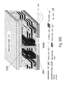
- FIG. 21A-21E are drawing illustrations of polysilicon select devices for 3D memory and peripheral circuits at the bottom according to some embodiments of the current invention.
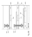
- FIG. 22A-22F are drawing illustrations of polysilicon select devices for 3D memory and peripheral circuits at the top according to some embodiments of the current invention.
- FIG. 23A-23D are drawing illustrations of a monolithic 3D SRAM according to some embodiments of the current invention.
- Section 1 Monolithic 3D DRAM.
- DRAMs 3D Dynamic Random Access Memories
- Some embodiments of this invention may involve floating body DRAM. Background information on floating body DRAM and its operation is given in “Floating Body RAM Technology and its Scalability to 32 nm Node and Beyond,” Electron Devices Meeting, 2006 . IEDM ' 06 . International , vol., no., pp. 1-4, 11-13 Dec. 2006 by T. Shino, N. Kusunoki, T.
- excess holes 102 may exist in the floating body region 120 and change the threshold voltage of the memory cell transistor including source 104 , gate 106 , drain 108 , floating body region 120 , and buried oxide (BOX) 118 .
- the ‘0’ bit may correspond to no charge being stored in the floating body region 120 and may affect the threshold voltage of the memory cell transistor including source 110 , gate 112 , drain 114 , floating body region 120 , and buried oxide (BOX) 116 . This is shown in FIG. 1( b ) .
- the difference in threshold voltage between the memory cell transistor depicted in FIG. 1( a ) and FIG. 1( b ) may manifest itself as a change in the drain current 134 of the transistor at a particular gate voltage 136 . This is described in FIG. 1( c ) .
- This current differential 130 may be sensed by a sense amplifier circuit to differentiate between ‘0’ and 1 ′ states and thus function as a memory bit.
- FIGS. 2A-M describe a flow to construct a horizontally-oriented monolithic 3D DRAM (Dynamic Random Access Memory).
- This monolithic 3D DRAM utilizes the floating body effect and double-gate transistors.
- One mask is utilized on a “per-memory-layer” basis for the monolithic 3D DRAM concept shown in FIG. 2A-M , while other masks are shared between different layers.
- the process flow may include several steps that occur in the following sequence.
- FIG. 2A illustrates the structure after Step (A).
- This presented process flow suggests the use of tungsten wiring or other refractory metal so the following process steps could include high temperature steps. These high temperature steps may include higher than 400° C. such as 800° C. or even 900° C. for dopant activation or damage annealing steps. Optical annealing and shielding may also be utilized, as described in the referenced patents. So the peripheral circuits activation could be delayed to those later high temperature steps.
- a wafer of p ⁇ Silicon 206 has an oxide layer 208 grown or deposited above it. Following this, hydrogen is implanted into the p ⁇ Silicon wafer at a certain depth indicated by 210 . Alternatively, some other atomic species such as Helium could be (co-)implanted. A portion of this hydrogen implanted p ⁇ Silicon wafer 206 may form the top layer 212 .
- the bottom layer 214 may include the peripheral circuits 202 with oxide layer 204 .
- the top layer 212 may be flipped and bonded to the bottom layer 214 using oxide-to-oxide bonding.
- FIG. 2C illustrates the structure after Step (C).
- the stack of top and bottom wafers after Step (B) may be cleaved at the hydrogen plane 210 using either an anneal or a sideways mechanical force or other means.
- a CMP (Chemical Mechanical Polishing) process may then be conducted.
- a single-crystal transferred p ⁇ layer 207 exists atop the peripheral circuits, and this has been achieved using layer-transfer techniques.
- a defect anneal step at about 800° C. could be applied to repair defects caused to the layer transferred p ⁇ layer 207 from the ion implant step used for the layer transfer.
- the thickness of transferred p ⁇ layer 207 could be set to be very thin, such as, for example, 5 nm or less and could be few tens of nm such as 50 nm or 100 nm or even thicker. In many case the preference could be for thin or very thin to reduce the aspect ratio of the following deep etch steps. These will be true for the many architectures and flow/structure variations presented hereinafter.
- FIG. 2E illustrates the structure after Step (E).
- An oxide layer 220 may be deposited atop the structure obtained after Step (D).
- a first layer of Si/SiO 2 222 is therefore formed atop the peripheral circuit layer 202 .
- the composition of the ‘SiO 2 ’ layer within the stacked Si/SiO 2 layers such as Si/SiO 2 222 may be insulators or dielectrics other than silicon dioxide such as, for example, a low-k dielectric, carbon containing silicon oxides, amorphous carbon.
- the thickness of the ‘SiO 2 ’ insulator layer within the stacked Si/SiO 2 layers such as Si/SiO 2 222 may be adjusted to minimize layer to layer, strata to strata disturb mechanisms, and may include thicknesses of 50 nm, 75 nm, 100 nm, 150 nm, 200 nm, 500 nm, and less than 1000 nm.
- a thin conductive layer such as a metal, may also be formed between the two bonding oxides to form a field shield to mitigate layer to layer, strata to strata disturb mechanisms, and may be electrically floating or tied to a bias, such as ground or Vdd.
- additional Si/SiO 2 layers 224 and 226 are formed atop Si/SiO 2 layer 222 .
- a rapid thermal anneal (RTA) or spike anneal or flash anneal or laser anneal may then be done to activate all implanted layers 222 , 224 and 226 (and possibly also the peripheral circuit layer 202 ).
- the layers 222 , 224 and 226 may be annealed layer-by-layer as soon as their implantations are done using a laser anneal system.
- the stacked Si/SiO 2 layers, such as Si/SiO 2 222 may alternatively be formed by successive ion implants of oxygen atoms/ions to various depths from the top surface of a mono-crystalline silicon wafer/substrate and then heat treated to form oxide layers thus forming silicon layers in-between the oxide layers, a layered ‘SIMOX’ process approach.
- the structure may include p ⁇ regions 219 and N+ regions 217 , any may be separated in the vertical direction from other conductive regions by a silicon oxide.
- Gate dielectric 228 and gate electrode 230 may be, for example, a HKMG structure or a TEL SPA radical oxidation oxide and an appropriate work function electrode, for example, tungsten, degenerately doped polysilicon or amorphous silicon.
- an appropriate work function electrode for example, tungsten, degenerately doped polysilicon or amorphous silicon.
- FIG. 2I illustrates the structure after Step (I).
- a silicon oxide layer 232 may then be deposited and planarized. For clarity, the silicon oxide layer is shown transparent in the figure, along with word-line (WL) and source-line (SL) regions.
- Bit-line (BL) contacts 234 are formed by etching and deposition. These BL contacts may be shared among all layers of the memory. Bit line contacts may be formed, for example, as sidewall structures or end-wall structures, with various overlaps as required by the process and layout.
- SL contacts can be made into stair-like structures using techniques described in “Bit Cost Scalable Technology with Punch and Plug Process for Ultra High Density Flash Memory,” VLSI Technology, 2007 IEEE Symposium on , vol., no., pp. 14-15, 12-14 Jun. 2007 by Tanaka, H.; Kido, M.; Yahashi, K.; Oomura, M.; et al., following which contacts can be constructed to them. Formation of stair-like structures for SLs could be done in steps prior to Step (K) as well.
- FIG. 2L shows cross-sectional views of the array for clarity. The double-gated transistors in FIG. 2 L can be utilized along with the floating body effect for storing information.
- FIG. 2L shows cross-sectional views of the array for clarity. The double-gated transistors in FIG. 2 L can be utilized along with the floating body effect for storing information.
- FIG. 2M shows an illustration of a memory cell of the floating body RAM array with two gates, such as gate electrode 230 and gate dielectric 228 , on either side of the p ⁇ region 219 .
- Insulator region SiO 2 238 may provide strata to strata isolation.
- a floating-body DRAM has thus been constructed, with (1) horizontally-oriented transistors—i.e., current flowing in substantially the horizontal direction in transistor channels, (2) some of the memory cell control lines, e.g., source-lines SL, constructed of heavily doped silicon and embedded in the memory cell layer, (3) side gates simultaneously deposited over multiple memory layers, and (4) monocrystalline (or single-crystal) silicon layers obtained by layer transfer techniques such as ion-cut.
- FIGS. 3A-K describe another process flow to construct a horizontally-oriented monolithic 3D DRAM.
- This monolithic 3D DRAM utilizes the floating body effect and double-gate transistors.
- No mask is utilized on a “per-memory-layer” basis for the monolithic 3D DRAM concept shown in FIGS. 3A-K , and all other masks are shared between different layers.
- the process flow may include several steps in the following sequence.
- FIG. 3A shows a drawing illustration after Step (A).
- FIG. 3B illustrates the structure after Step (B).
- a wafer of p ⁇ Silicon 308 has an oxide layer 306 grown or deposited above it. Following this, hydrogen may be implanted into the p ⁇ Silicon wafer at a certain depth indicated by 314 . Alternatively, some other atomic species such as Helium could be (co-)implanted.
- This hydrogen implanted p ⁇ Silicon wafer 308 may form top layer 310 .
- the bottom layer 312 may include the peripheral circuits 302 with oxide layer 304 .
- the top layer 310 may be flipped and bonded to the bottom layer 312 using oxide-to-oxide bonding.
- Step (B) The bonded stack of top and bottom wafers after Step (B) may be cleaved at the hydrogen plane 314 using either a anneal or a sideways mechanical force or other means. A CMP process may then be conducted. A layer of silicon oxide 318 may be deposited atop the p ⁇ Silicon layer 316 . Thus, a single-crystal p ⁇ Si layer 316 may be atop the peripheral circuits, and this has been achieved using layer-transfer techniques.
- Step (D) FIG. 3D illustrates the structure after Step (D). Using methods similar to Step (B) and (C), multiple p ⁇ silicon layers 320 may be formed with silicon oxide layers in between.
- the composition of the ‘SiO 2 ’ layer within the stacked p-Si/SiO 2 layers may be insulators or dielectrics other than silicon dioxide such as, for example, a low-k dielectric, carbon containing silicon oxides, amorphous carbon.
- the thickness of the ‘SiO 2 ’ insulator layer within the stacked p-Si/SiO 2 layers may be adjusted to minimize layer to layer, strata to strata disturb mechanisms, and may include thicknesses of 50 nm, 75 nm, 100 nm, 150 nm, 200 nm, 500 nm, and less than 1000 nm.
- a thin conductive layer such as a metal, may also be formed between the two bonding oxides to form a field shield to mitigate layer to layer, strata to strata disturb mechanisms, and may be electrically floating or tied to a bias, such as ground or Vdd.
- the stacked Si/SiO 2 layers may alternatively be formed by successive ion implants of oxygen atoms/ions to various depths from the top surface of a mono-crystalline silicon wafer/substrate and then heat treated to form oxide layers thus forming silicon layers in-between the oxide layers, a layered ‘SIMOX’ process approach.
- Gate dielectric 326 and gate electrode 324 may be deposited following which a CMP may be done to planarize the gate electrode 324 regions. Lithography and etch are utilized to define gate regions.
- Gate dielectric 326 and gate electrode 324 may be, for example, a HKMG structure or a TEL SPA radical oxidation oxide and an appropriate work function electrode, for example, tungsten, degenerately doped polysilicon or amorphous silicon.
- Step (G) FIG. 3G illustrates the structure after Step (G) including N+ silicon regions 328 .
- Step (F) p ⁇ regions not covered by the gate may be implanted to form n+ regions.
- Spacers may be utilized during this multi-step implantation process and layers of silicon present in different layers of the stack may have different spacer widths to account for lateral straggle of buried layer implants.
- a silicon oxide layer 330 may be deposited and planarized. For clarity, the silicon oxide layer is shown transparent, along with word-line (WL) 332 and source-line (SL) 334 regions.
- Bit-line (BL) contacts 336 are formed by etching and deposition. These BL contacts may be shared among the layers of memory. Bit line contacts may be formed, for example, as sidewall structures or end-wall structures, with various overlaps as required by the process and layout.
- BLs 338 may be constructed. Contacts may be made to BLs, WLs and SLs of the memory array at its edges. SL contacts can be made into stair-like structures using techniques described in “Bit Cost Scalable Technology with Punch and Plug Process for Ultra High Density Flash Memory,” VLSI Technology, 2007 IEEE Symposium on , vol., no., pp. 14-15, 12-14 Jun.
- FIG. 3K shows cross-sectional views of the array for clarity. Double-gated transistors may be utilized along with the floating body effect for storing information. A floating-body DRAM has thus been constructed, with (1) horizontally-oriented transistors—i.e.
- transistor channels (2) some of the memory cell control lines, e.g., source-lines SL, constructed of heavily doped silicon and embedded in the memory cell layer, (3) side gates simultaneously deposited over multiple memory layers, and (4) monocrystalline (or single-crystal) silicon layers obtained by layer transfer techniques such as ion-cut.
- some of the memory cell control lines e.g., source-lines SL, constructed of heavily doped silicon and embedded in the memory cell layer
- side gates simultaneously deposited over multiple memory layers and (4) monocrystalline (or single-crystal) silicon layers obtained by layer transfer techniques such as ion-cut.
- Various other types of layer transfer schemes and anneal/shielding techniques that have been described in the referenced and incorporated patents can be utilized for construction of various 3D DRAM structures.
- buried wiring i.e. where wiring for memory arrays is below the memory layers but above the periphery, may also be used.
- other variations of the monolithic 3D DRAM concepts are possible, such as, for example, forming the periphery circuits above and/or below the memory stack layers.
- the positive charge stored may decrease over time due to the diode leakage current of the p-n junctions formed between the floating body and n+ regions and due to charge recombination.
- a method to refresh all memory cells in parallel have been described in “Autonomous Refresh of Floating Body Cell (FBC)”, Ohsawa et al., pp. 801-804, International Electron Device Meeting, 2008 (“Ohsawa”), U.S. Pat. No. 7,170,807 “Data Storage Device and Refreshing Method for Use with Such Device”, Fazan et al. (“Fazan”) and in U.S. Pat. No.
- Widjaja A Semiconductor Memory Device Having an Electrically Floating Body Transistor”, Widjaja and Or-Bach (“Widjaja”), which are incorporated by reference herein in entirety.
- Ohsawa and Fazan teach an autonomous refresh method by applying a periodic gate and drain voltage pulses and Widjaja describes a parallel refresh method by applying a bias to the back bias terminal.
- FIG. 4A is a drawing illustration of the cross-section of a memory cell 450 in a memory layer of the 3D DRAM device shown in FIG. 2L .
- FIG. 4B is a drawing illustration of the equivalent circuit representation of the memory cell shown in FIG. 4A .
- the refresh operation will be described with reference to FIGS. 4A and 4B , although the same principle applies to other 3D DRAM described herein, for example, as shown in FIG. 3K .
- memory cell 450 may include a floating body 424 of p-type conductivity.
- the floating body 424 may be bounded by an insulating region 422 , n+ regions 416 and 418 , and by the surface 414 .
- a gate 460 may be positioned in-between the n+ regions 416 and 418 , and may be insulated from the floating body region 424 by an insulating layer 462 , and may be connected to gate connectivity 470 .
- n-p-n bipolar device 430 formed by n+ region 416 (the collector region), floating body 424 (the base region), and n+ region 418 (the emitter region).
- the collector n+ region 416 can be connected to the SL terminal 472 and the emitter region 418 can be connected to the BL terminal 474 , or vice versa.
- the refresh operation can be performed by applying a positive voltage to the collector n+ region 416 while simultaneously grounding the emitter region 418 .
- the refresh operation is relatively independent of the voltage applied to gate 460 . In some embodiments of the invention, the gate may be grounded.
- the bipolar device 430 will be turned on.
- the voltage across the reversed biased p-n junction between the floating body 424 and the collector n+ region 416 may cause a small current to flow across the junction.
- Some of the current may be in the form of hot carriers accelerated by the electric field across the junction. These hot carriers may collide with atoms in the semiconductor lattice which may generate hole-electron pairs in the vicinity of the junction.
- the electrons may be swept into the collector n+ region 416 by the electric field, while the holes may be swept into the floating body region 424 .
- the hole current flowing into the floating region 424 (usually referred to as the base current) will maintain the logic-1 state data.
- the efficiency of the refresh operation can be enhanced by designing the bipolar device formed by collector n+ region 416 , floating region 424 , and emitter region 418 to be a low-gain bipolar device, where the bipolar gain is defined as the ratio of the collector current flowing out of collector n+ region 416 to the base current flowing into the floating region 424 .
- FIG. 4C is a drawing illustration of the energy band diagram of the intrinsic n-p-n bipolar device 430 when the floating body region 424 is positively charged and a positive bias voltage is applied to the collector n+ region 416 .
- the dashed lines indicate the Fermi levels in the various regions of the n-p-n transistor 430 .
- the Fermi level is located in the band gap between the solid line 417 indicating the top of the valance band (the bottom of the band gap) and the solid line 419 indicating the bottom of the conduction band (the top of the band gap) as is well known in the art.
- the positive charge in the floating body region lowers the energy barrier of electron flow into the base region.
- the electrons will be swept into the collector n+ region 416 due to the positive bias applied to the collector n+ region 416 .
- the electrons may be accelerated and create additional hot carriers (hot hole and hot electron pairs) through an impact ionization mechanism.
- the resulting hot electrons flow into the collector n+ region 416 while the resulting hot holes will subsequently flow into the floating body region 424 .
- This process restores the charge on floating body 424 and will maintain the charge stored in the floating body region 424 which will keep the n-p-n bipolar transistor 430 on for as long as a positive bias is applied to the collector n+ region 416 .
- FIG. 4D shows the energy band diagram of the intrinsic n-p-n bipolar device 430 when the floating body region 424 is neutrally charged and a bias voltage is applied to the collector n+ region 416 .
- the energy level of the band gap bounded by solid lines 417 A and 419 A is different in the various regions of n-p-n bipolar device 430 .
- Solid line 423 indicates, for reference purposes, the energy barrier between the emitter region 418 and the floating body region 424 . The energy barrier prevents electron flow from the emitter region 418 to the floating body region 424 .
- the n-p-n bipolar device 430 will remain off.
- FIG. 4E is a drawing illustration of an exemplary refresh operation in an exemplary array 480 formed by a plurality of memory cell 450 (corresponds to a memory layer of the 3D DRAM device, such as those described herein) is shown in FIG. 4E .
- Present in FIG. 4E are word lines (WLs) 470 a through 470 n , source lines (SLs) 472 a through 472 n , and bit lines (BLs) 474 a through 474 p .
- each of the word lines 470 a through 470 n is associated with a single row of memory cells 450 and is coupled to the gate 460 of each memory cell 450 in that row.
- each of the source lines 472 a through 472 n is associated with a single row of memory cells 450 and is coupled to the collector n+ region 416 of each memory cell 450 in that row.
- Each of the bit lines 474 a through 474 p is associated with a single column of memory cells 450 and is coupled to the emitter region 418 of each memory cell 450 in that column.
- there is no individually selected memory cell there is no individually selected memory cell. Rather cells are selected in rows by the source lines 472 a through 472 n and may be selected as individual rows, as multiple rows, or as all of the rows comprising array 480 . Cells can also be selected in columns by bit lines 474 a through 474 p and may be selected as individual columns, as multiple columns, or as all of the columns comprising array 480 .
- exemplary array 480 is shown as a single continuous array in FIG. 4E , that many other organizations and layouts are possible like, for example, word lines may be segmented or buffered, bit lines may be segmented or buffered, source lines may be segmented or buffered, the array 480 may be broken into two or more sub-arrays, control circuits such as word decoders, column decoders, segmentation devices, sense amplifiers, write amplifiers may be arrayed around exemplary array 480 or inserted between sub-arrays of array 480 .
- word decoders such as word decoders, column decoders, segmentation devices, sense amplifiers, write amplifiers
- sense amplifiers sense amplifiers
- write amplifiers may be arrayed around exemplary array 480 or inserted between sub-arrays of array 480 .
- FIG. 4E Also shown in FIG. 4E are multiplexers 440 a through 440 n and voltage waveforms 442 a through 442 n .
- a constant positive bias can be applied to the collector n+ regions 416 of memory cells 450 (through SL terminal 472 ).
- a periodic pulse of positive voltage can be applied to the collector n+ regions 416 of memory cells 450 through SL terminal 472 as opposed to applying a constant positive bias to reduce the power consumption of the memory cell 450 .
- FIG. 4E further shows multiplexers 440 a through 440 n each coupled to one of the source lines 472 a through 472 n that determine the bias voltages applied to SL terminals 472 a through 472 n , which will be determined by different operating modes.
- the pulsing of the voltage on the SL terminals may be controlled, for example, by applying pulses of logic signals such as, for example, waveforms 442 a through 442 n to the select input of multiplexers 440 a through 440 n thereby selecting, for example, ground (0.0 volts) or a power supply voltage such as V CC .
- logic signals such as, for example, waveforms 442 a through 442 n
- V CC power supply voltage
- FIG. 4F is a drawing illustration of another method to provide voltage pulses to SL terminals 472 a through 472 n of exemplary array 480 of memory cells 450 .
- the positive input signals to multiplexers 440 a through 440 n may be generated by voltage generator circuits 444 a through 444 n coupled to one input of each of the multiplexers 440 a through 440 n .
- a single voltage generator circuit may be coupled to each of the multiplexers 440 a through 440 n reducing the amount of overhead circuitry required to refresh the memory cells 450 of array 480 .
- waveforms 442 a through 442 n are possible including, for example, applying the waveforms 442 a through 442 n at different times, or applying them simultaneously, or coupling the select inputs of multiplexers 442 a through 442 n together and applying a single pulsed waveform to all of the multiplexers 442 a through 442 n simultaneously (not shown in the figure).
- FIG. 4G is a drawing illustration of a reference generator circuit suitable for use as reference generator circuits 444 a through 444 n in FIG. 4F .
- the reference generator includes reference cell 453 , which may consist of a modified version of memory cell 450 described above with region 425 of p-type conductivity.
- the p-type region 425 allows for a direct sensing of the floating body region 424 potential.
- P-type region 425 is drawn separately even though it has the same conductivity type as floating body region 424 because it may be doped differently, such as, for example, a higher concentration of doping than floating body region 424 , to facilitate contacting it.
- the reference cell 453 for example can be configured to be in state logic-1 where the potential of the floating body region 424 is positive, for example at +0.5V.
- the potential sensed through the p-type region is then compared with a reference value V REF , e.g. +0.5V, by operational amplifier 427 . If the potential of the floating body region 424 is less than the reference value, the voltage applied to the SL terminal 472 (which is connected to drain n+ region 416 of the reference cell 453 and is also connected to collector n+ region 416 of the memory cell 450 ) may be increased by operational amplifier 427 until the potential of the floating body region 424 reaches the desired reference voltage.
- Reference voltage V REF may be generated in many different ways such as, for example, using a band gap reference, a resistor string, a digital-to-analog converter, and so on. Similarly alternate voltage generators of types known in the art may be used.
- read circuitry 499 a may be coupled to the bit line 474 a .
- a reading circuit 499 b through 499 p (not shown in FIGS. 4E and 4F ) may be coupled to each bit of the bit lines 474 b through 474 p , while in other embodiments reading circuit 499 a may be shared between multiple columns using a decoding scheme (not shown).
- FIG. 5A is a drawing illustration of another embodiment of a gateless memory cell 5150 in a memory layer of the 3D DRAM device.
- FIG. 5B is a drawing illustration of the equivalent circuit representation of the memory cell shown in FIG. 5A .
- memory cell 5150 includes a floating body 524 of p-type conductivity. The floating body 524 is bounded by the insulator layer 522 , n+ regions 516 and 518 , and by the insulator layer 526 .
- a difference to the memory cell 450 shown in FIG. 4A is that no gate electrode exists in memory cell 5150 .
- the n+ regions 516 and 518 may be configured differently, for example, the n+ region acting as the emitter region (n+ region 518 ) is typically more heavily doped than the n+ collector region (n+ region 516 ).
- floating body DRAM cell 5150 may include an n-p-n bipolar device 5130
- n-p-n bipolar device 5130 may include n+ region 516 (the collector region), floating body 524 (the base region), and n+ region 518 (the emitter region).
- the collector region can be connected to the SL terminal 572 and the emitter region can be connected to the BL terminal 574 , or vice versa.
- FIG. 5C is a drawing illustration of an exemplary memory array 5180 which will be used in subsequent drawing figures to illustrate the various operations that may be performed on memory cell 5150 when arranged in an array to create a memory device.
- Memory array 5180 comprises in part representative memory cells 5150 a , 5150 b , 5150 c , and 5150 d .
- representative memory cell 5150 a will represent the selected cell while the representative memory cells 5150 b , 5150 c , and 5150 d will represent the various cases of unselected memory cells sharing a row, sharing a column, or sharing neither a row nor a column respectively with selected representative memory cell 5150 a .
- representative memory cell 5150 a will be on the selected row or column.
- the memory cell states are represented by the charge in the floating body 524 , which modulates the intrinsic n-p-n bipolar device 5130 .
- the collector region can be connected to the SL terminal 572 and the emitter region can be connected to the BL terminal 574 , or vice versa. If cell 5150 has a substantial number of holes stored in the body region 524 , then the memory cell may have a higher bipolar current (e.g. current flowing from BL to SL terminals during read operation) compared to if cell 5150 does not store an appreciable amount of holes in body region 524 .
- the positive charge stored in the body region 524 may decrease over time due to the p-n diode leakage formed by floating body 524 and n+ regions 516 and 518 , and due to charge recombination.
- a refresh operation applied to the entire memory array 5180 is illustrated in FIG. 5D .
- the refresh operation on memory cell 5150 can be performed by applying a positive bias to the collector region 516 (connected for example to SL terminal 572 ) while grounding the emitter region 518 (connected for example to BL terminal 574 ). If floating body 524 is substantially positively charged (i.e. in a state logic-1), the n-p-n bipolar transistor 5130 will be turned on.
- a fraction of the bipolar transistor 5130 current will then flow into floating body region 524 and maintain the state logic-1 data.
- the efficiency of the refresh operation can be enhanced by designing the bipolar transistor 5130 to be a low-gain bipolar device, where the bipolar gain is defined as the ratio of the collector current flowing out of collector region 516 to the base current flowing into floating body region 524 .
- a periodic pulse of positive voltage can be applied to the SL terminal 572 as opposed to applying a constant positive bias to reduce the power consumption of the memory cell 5150 .
- source line terminals 572 a through 572 n may be biased at +1.2V and bit lines 574 a through 574 p may be biased to 0.0V. This refreshes substantially all of the cells in memory array 5180 .
- a single row operation can also be performed on memory array 5180 as illustrated in FIG. 5E , where selected source line terminal 572 a may be biased at +1.2V while the unselected source line terminals 572 b (not shown) through 572 n may be biased at Vdd/2, and bit lines 574 a through 574 p may be biased to 0.0V. This refreshes substantially all of the selected cells in memory array 5180 .
- a single memory cell read operation is illustrated in FIG. 5F .
- the read operation for memory cell 5150 a can be performed by sensing the current of the bipolar device 5130 by applying a positive voltage to the selected BL terminal 574 a and zero voltage to the selected SL terminal 572 a .
- the positive voltage applied to the selected BL terminal may be less than or equal to the positive voltage applied to the SL terminal during the refresh operation.
- the unselected BL terminals may remain at Vdd/2 and the unselected SL terminals may remain at a positive voltage.
- FIG. 5F shows the bias condition for the selected memory cell 5150 a and unselected memory cells 5150 b , 5150 c , and 5150 d in memory array 5180 .
- about 0.0 volts may be applied to the selected SL terminal 572 a while about +1.2V is applied to the unselected source line terminals 572 b (not shown) through 572 n
- about +1.2 volts is applied to the selected BL terminal 574 a while 0.0V is applied to the unselected bit line terminals 574 b through 574 p .
- These voltage levels are exemplary only and may vary from embodiment to embodiment.
- the n+ regions 516 and 518 can be configured asymmetrically such that the current flowing through the selected cell 5150 a during read operation (from the BL terminal 574 to the SL terminal 572 ) may be higher than the refresh current flowing through the unselected memory cells (from the SL terminal 572 to the BL terminal 574 ), although similar bias conditions are applied to selected and unselected memory cells 5150 (with the bias conditions are reversed between the BL and SL terminals of the selected and unselected memory cells 5150 ).
- the SL terminal 572 a and the BL terminal 574 p are both biased to 0.0V and consequently these cells will not be at the refresh mode.
- read operation is accomplished much faster (in the order of nanoseconds) when compared to the lifetime of the charge in the floating body 524 (in the order of milliseconds), it should cause little disruption to the charge stored in the floating body.
- a positive voltage is applied to the BL terminal 574 a and SL terminal 572 n .
- No base current will flow into the floating body 524 because there is no appreciable potential difference between SL terminal 572 and BL terminal 574 (i.e. the emitter and collector terminals of the n-p-n bipolar device 5130 ).
- the read operation is accomplished much faster (in the order of nanoseconds) compared to the lifetime of the charge in the floating body 524 (in the order of milliseconds), it should cause little disruption to the charge stored in the floating body.
- both the SL terminal 572 n will remain positively charged and the BL terminal 574 p may remain grounded.
- Representative memory cell 5150 d will be in the refresh mode, where memory cells in state logic-1 will maintain the charge in floating body 524 because the intrinsic bipolar device 5130 will generate hole current to replenish the charge in floating body 524 , while memory cells in state logic-0 will remain in neutral state.
- FIG. 5G illustrates a single row write logic-0 operation.
- the selected row SL terminal 572 a may be biased negatively at about ⁇ 0.5V while the unselected row SL terminals 572 b (not shown) through 572 n may be biased at about +1.2V and all the BL terminals 574 a through 574 p may be biased at 0.0V.
- This causes the selected cells such as representative memory cells 5150 a and 5150 b to have their bipolar devices turn on due to forward bias on the floating body 524 to collector region 516 , thereby evacuating the holes from the floating body 524 .
- the SL terminal 572 is at +1.2V and the BL terminal 574 is at 0.0V, which corresponds to the refresh operation described above.
- a write logic-0 operation can also be performed on a column basis by applying a negative bias to the BL terminal 574 as opposed to the SL terminal 572 .
- the SL terminal 572 will be zero or positively biased. Under these conditions, substantially all memory cells sharing the same BL terminal 574 will be written into state logic-0 and substantially all the other cells will be in the refresh operation.
- a write logic-1 operation can be performed on memory cell 5150 through an impact ionization mechanism as described in FIG. 5H .
- An example of the bias condition of the selected memory cell 5150 a under impact ionization write logic-1 operation is illustrated in FIG. 5H .
- a positive bias may be applied to the BL terminal 574 , while zero voltage may be applied to the selected SL terminal 572 .
- the positive bias applied to the BL terminal 574 may be greater than the positive voltage applied to the SL terminal 572 during refresh operation.
- the positive bias applied to the BL terminal is large enough to turn on bipolar device 5130 regardless of the initial state of the data in selected memory cell 5150 a . This results in a base hole current to the floating body 524 of the selected memory cell 5150 a charging it up to a logic-1 state.
- the following bias conditions may be applied to the selected memory cell 5150 a : a potential of about 0.0 volts is applied to selected SL terminal 572 a and a potential of about +2.0 volts is applied to selected BL terminal 574 a .
- the following bias conditions may be applied to the unselected terminals: about +1.2 volts is applied to SL terminals 572 b (not shown) through 572 n , and about 0.0 volts is applied to BL terminals 574 b through 574 p .
- FIG. 5H shows the bias condition for the selected and unselected memory cells in memory array 5180 .
- the various voltage bias levels above are exemplary only. They will vary from embodiment to embodiment as a function of both design choice and the process technology used.
- SL terminal 572 a and BL terminal 574 p may be grounded.
- Bipolar device 5130 will be off and the memory cell 5150 b will not be at the refresh mode.
- write operation is accomplished much faster (in the order of nanoseconds) compared to the lifetime of the charge in the floating body 524 (in the order of milliseconds), it should cause little disruption to the charge stored in the floating body.
- a greater positive voltage is applied to the BL terminal 574 a and a lesser positive voltage is applied to SL terminal 572 n .
- Less base current will flow into the floating body 524 than in selected memory cell 5150 a because of the lower potential difference between SL terminal 572 and BL terminal 574 (i.e. the emitter and collector terminals of the n-p-n bipolar device 5130 ).
- the write operation is accomplished much faster (in the order of nanoseconds) compared to the lifetime of the charge in the floating body 524 (in the order of milliseconds), it should cause little disruption to the charge stored in the floating body.
- representative memory cell 5150 d sharing neither the same column nor the same row as the selected memory cell 5150 a , the SL terminal 572 is positively charged and the BL terminal is grounded.
- Representative memory cell 5150 d will be at refresh mode, where memory cells in state logic-1 will maintain the charge in floating body 524 because the intrinsic bipolar device 5130 will generate hole current to replenish the charge in floating body 524 and where memory cells in state logic-0 will remain in neutral state.
- the various voltage bias levels above are exemplary only. They will vary from embodiment to embodiment as a function of both design choice and the process technology used. Also, the first conductivity type may be changed from p-type to n-type and the second conductivity type may be changed from n-type to p-type, and the polarities of the applied biases may be reversed. Thus the invention is not to be limited in any way except by the appended claims.
- SRAM Static Random Access Memory
- FIG. 6 is a drawing illustration of a Floating Body memory cell 50 with a buried well region 12 , where applying a back bias (through terminal 78 ) to the n-type buried well region 12 (also referred to as the back bias region 12 ) may maintain the charge stored in the floating body region 24 .
- FIG. 6 may be found as FIG. 1A of the US Patent Publication No. 2012/0230123.
- the floating body 24 may be P type
- the drain 16 and source 18 may be N type
- the gate oxide 62 and the gate 60 may include, such as, for example, SiO2 and polysilicon or HKMG, and the floating body transistor may be isolated by deep trench isolations 26 .
- the user terminals for writing and reading the memory may be drain 72 , source 74 , and gate 70 .
- the top surface 14 of the mono-crystal may be the upper side of the wafer.
- Interconnect layers such as is known by those skilled in the art, may be formed to connect the memory cell (not shown).
- a key to the two charge states holding of the floating body memory is the application of a positive back bias, such as 1.2 volt, to the back bias region 12 (through terminal 78 ).
- the NPN bipolar transistor formed between the n-type back bias region 12 , the p-type floating body region 24 , and the n-type drain 16 or source 18 is the key to the unique charging mechanism as described in these referenced art and before in respect to at least FIGS.
- a key to the self-charging mechanism is having the structure meet the formula (M ⁇ 1)* ⁇ ⁇ 1, which is related to the structure feature and design of the memory cell 50 , where ⁇ is the gain of the bipolar transistor and M is the impact ionization multiplication factor.
- the two stable states may be two stable floating body charge levels.
- the structure and process flow have similarities to a previous description, such as FIGS. 3A-K and associated text.
- a device and method to form back-bias region for 3D floating body memory architecture is described below.
- FIG. 7A is a drawing illustration of an embodiment of a three-dimensional view of a 3D RAM structure and device architecture prior to the interconnect stage of the process flow (similar to FIG. 7G )
- FIG. 7B is a drawing illustration of cross-sectional cut I of FIG. 7A
- FIG. 7C is a drawing illustration of cross-sectional cut II of FIG. 7A
- FIG. 7D is a drawing illustration of cross-sectional cut II of FIG. 7A with the gate material and perforated gate dielectric overlap/under-lap depicted.
- FIGS. 7A is a drawing illustration of an embodiment of a three-dimensional view of a 3D RAM structure and device architecture prior to the interconnect stage of the process flow (similar to FIG. 7G )
- FIG. 7B is a drawing illustration of cross-sectional cut I of FIG. 7A
- FIG. 7C is a drawing illustration of cross-sectional cut II of FIG. 7A
- FIG. 7D is a drawing illustration of cross-sectional cut II of FIG
- FIG. 7A, 7B, 7C, and 7D may include n+ silicon regions 728 , silicon oxide regions 722 , gate regions 760 , back-bias regions 712 , gate dielectric regions 762 , p ⁇ channel regions 724 , isolation dielectric 706 , gate dielectric openings 711 , and peripheral circuits 702 .
- FIG. 7D may include a shadowed overlay image of gate regions 760 and gate dielectric openings 711 depicting the overlap and underlaps of these regions with respect to p ⁇ channel regions 724 .
- FIG. 7B may include surface 713 , wherein back-bias region 712 may be in physical contact and make electrical connection to p ⁇ channel region 724 .
- a floating body transistor in the stack may include a single side gate (gate regions 760 ) on one side of floating body p ⁇ channel region 724 and a back-bias region 712 formed on the other side of the floating body p ⁇ channel region 724 .
- Gate region 760 may be insulated from the floating body p ⁇ channel region 724 with a gate dielectric regions 762 , yet still modulate the channel.
- the back-bias is not horizontal such as in FIG. 4A but rather vertical such as back bias regions 712 of FIG. 7B .
- N+ silicon regions 728 may be connected and utilized as either a source or drain to help form the two stable states floating body transistor.
- FIGS. 7A-7D A process flow that may be utilized to form the structure shown in FIGS. 7A-7D is described as follows. Many steps may be similar to those used to form the structure shown in FIG. 3E .
- FIG. 7E multiple mono-crystalline p ⁇ silicon layers may be formed with silicon oxide layers in-between and then lithography and etch processes may be utilized to make a structure, such as, for example, as shown in FIG. 7E .
- p ⁇ silicon regions 721 and silicon oxide regions 722 may be stacked and formed above peripheral circuits 702 .
- Processes to form the structure in FIG. 7E may include the steps described with respect to FIGS. 3A to 3E herein.
- Peripheral circuits 702 may be constructed with tungsten, or conventional aluminum/copper, wiring and may have isolation and/or bonding oxide above it (in-between the top metallization/wiring of peripheral circuits 702 and the bottom p-silicon region in the stack, such as isolation oxide 706 .
- the composition of the silicon oxide regions 722 within the stacked Si/SiO 2 layers may be insulators or dielectrics other than silicon dioxide such as, for example, a low-k dielectric, carbon containing silicon oxides, amorphous carbon.
- the thickness of silicon oxide regions 722 within the stacked Si/SiO 2 layers may be adjusted to minimize layer to layer, strata to strata disturb mechanisms, and may include thicknesses of 50 nm, 75 nm, 100 nm, 150 nm, 200 nm, 500 nm, and less than 1000 nm.
- a thin conductive layer, such as a metal may also be formed between the two bonding oxides to form a field shield to mitigate layer to layer, strata to strata disturb mechanisms, and may be electrically floating or tied to a bias, such as ground or Vdd.
- the stacked Si/SiO 2 layers may alternatively be formed by successive ion implants of oxygen atoms/ions to various depths from the top surface of a mono-crystalline silicon wafer/substrate and then heat treated to form oxide layers thus forming silicon layers in-between the oxide layers, a layered ‘SIMOX’ process approach.
- a perforated gate dielectric layer 762 (partially shown for clarity) may be formed which has gate dielectric openings 711 on one face of the p ⁇ silicon 721 and silicon oxide 722 layer stack, a gate electrode material may be deposited and CMP'd substantially to the top of the Si/SiO 2 stack.
- the gate dielectric may be grown on the exposed surfaces of p ⁇ silicon regions 721 (for example, with the TEL SPA tool radical oxidation oxide) or deposited substantially over the structure's surface, such as, for example, in the well-known HKMG formation processing, a lithographic step and etch of the deposited gate dielectric may thus form perforated gate dielectric layer 762 and gate dielectric openings 711 on one face of the p ⁇ silicon 721 and silicon oxide 722 layer stack and leave the gate dielectric intact another face of the p ⁇ silicon 721 and silicon oxide 722 layer stack.
- a gate electrode material such as, for example, doped amorphous or polysilicon, or the well-known metal stack of HKMG processing, may be deposited, thus bringing the conductive gate electrode material in direct contact and electrical connection with exposed faces of the p-silicon 721 , and forming a field effect device of gate electrode influence thru the gate dielectric of the eventual transistor p ⁇ channel regions 724 formed by portions of p-silicon 721 layers.
- the gate electrode material may be in-situ doped during deposition, or doped at a later step. CMP may be performed to planarize the gate electrode material.
- the top face of the topmost silicon oxide region 722 may have an etch stop/CMP stop material, such as, for example, SiN or a-carbon, placed on it at an earlier stage, so to provide a CMP stop, thus enabling the formation of separate gate and back bias control regions.
- an etch stop/CMP stop material such as, for example, SiN or a-carbon
- the width of the p ⁇ regions 721 near and under the gates are illustrated as being larger than the thickness, one skilled in the art would recognize that the reverse (i.e., thickness larger than width) could be formed to provide increased gate control of the transistor channel.
- n+ silicon regions 728 , gate regions 760 and back-bias regions 712 may be formed.
- the gate may be lithography defined.
- the widths of the gate structure regions and the gate dielectric openings 711 may be designed such that the gate structure regions will substantially always overlap the gate dielectric openings 711 .
- portions of p ⁇ regions 721 not covered by the gate structure regions photoresist may be implanted to form n+ regions 728 , and thus form p ⁇ channel regions 724 .
- This multi-step implantation process may utilize different implant energies.
- the gate may then be etched to define gate structure regions shown in FIG.
- a thermal annealing step such as an RTA or spike anneal or laser anneal or flash anneal, may be conducted to activate the n+ implanted doped regions.
- the optical anneal system such as the laser, spike, flash anneals, may be utilized to crystallize any deposited polysilicon or amorphous silicon (which may be used as a gate electrode material depending on process design choice).
- the structure valleys may be filled with a dielectric (not shown for clarity), such as, for example, SACVD oxides, and then CMP'd substantially to or partially into the topmost silicon oxide layer 722 of the Si/SiO2 stack, or substantially to or partially into the CMP/etch stop layer as previously discussed.
- a dielectric such as, for example, SACVD oxides
- horizontal floating gate transistors with separate gate and back bias control regions on the previously exposed sides of each p ⁇ transistor channel region, and horizontal select lines may be formed in a stack configuration.
- an inter-layer dielectric such as, for example silicon oxide or doped silicon dioxides, may be deposited and planarized. For clarity, the silicon oxide layer is shown transparent.
- Contacts to gate regions 760 and the associated local metallization gate connectivity 750 , as well as contacts to back-bias regions 712 and the associated local metallization back-bias connectivity 752 may be formed using known methods in the art.
- Source-Line (SL) connectivity 754 such as contacts and metal lines, may be formed by etching and deposition using known methods in the art. These SL contacts may be shared among the layers of memory. Gate connectivity 750 and back-bias connectivity 752 are not shown in FIG. 7I for clarity.
- the bit lines (BL) 756 are shown as a portion of the n+ silicon regions 728 . Bit line contacts may be formed, for example, as sidewall structures or end-wall structures, with various overlaps as required by the process and layout.
- gate connectivity 750 may be connected to form the WL-word select lines. Contacts may be made to BLs, WLs and SLs of the memory array at its edges. BL contacts can be made into stair-like structures using techniques described in “Bit Cost Scalable Technology with Punch and Plug Process for Ultra High Density Flash Memory,” VLSI Technology, 2007 IEEE Symposium on , vol., no., pp. 14-15, 12-14 Jun. 2007 by Tanaka, H.; Kido, M.; Yahashi, K.; Oomura, M.; et al., following which contacts can be constructed to them. Formation of stair-like structures for BLs could be done in steps prior to FIG. 7I .
- Electrical connection to the underlying peripheral circuits may be accomplished with vertical conductive vias, for example, the thru layer via or thru silicon via processes and structures, which may be described in the incorporated patent references or known by those skilled in the art.
- thermal vias may be utilized to carry heat, whether from processing or from operation, away from the upper layer without harming the underlying metallization or devices.
- FIG. 7J is a top view exemplary illustration of the floating body transistors sharing on one side of the Si/SiO 2 stacks (n+ regions 728 and floating body p ⁇ channel regions 724 ) gate regions 760 and on the other side of the Si/SiO 2 stacks back bias regions 712 connected to p ⁇ channel regions 724 in the openings of the perforated gate dielectric layer 762 .
- the back-bias regions act as the collector of the bipolar charging transistor as illustrated in FIG. 4B .
- Bipolar transistors that utilize a polysilicon collector with monocrystalline base and emitter are well known in the art to perform well.
- the contacts of the source line connectivity 754 are shown, but the metal lines, as well as the SL staircase and WL connectivity are not shown for clarity.
- Back-bias regions 712 may be mutually connected to a bias source.
- FIGS. 7A through 7J are exemplary only and are not drawn to scale. Such skilled persons will further appreciate that many variations are possible such as, for example, the Si/SiO2 stack may be formed with the N+ and p ⁇ regions already formed by stacking with 1-mask per stack layer processing as described, for example, in FIG. 2 herein. Further, it may not be necessary to overlap the implant gate structure regions and the gate dielectric openings 711 . Moreover, perforated gate dielectric layer 762 may not need to be perforated, and control of the back-bias effects may be performed thru the gate dielectric from an efield influence modulated by the back bias regions 712 , or by band bending with an Esaki diode structure.
- peripheral circuits may be on top of the memory stack layers rather than on the bottom, and connected accordingly.
- a prior to the n+ implant step anneal to repair damages that were formed during prior step such as layer transfer ion cut related damages and etch step related damages, may be performed.
- some of the memory global control lines could be implemented in the bottom base layer peripheral circuits 702 and connected to the upper memory structure as it is processed. This could be done for the back-bias connections.
- the base layers from the peripheral circuits 702 may provide the back-bias connection. In such case before depositing the gate electrode material, a contact to those connections would be etched in the soon to be back bias regions 712 .
- the impact ionization efficiency of the polysilicon collector in the architecture illustrated in FIGS. 7A-7D may typically be low (the (M ⁇ 1) factor is typically less than 10 ⁇ 3 ). As a result, a large current may be required in the holding operation.
- the source region ( 16 of FIG. 6 ) or the drain region ( 18 of FIG. 6 ), which may be either of the n+ regions 728 on the sides of p ⁇ channel regions 724 may be used as the collector region/node and the polysilicon region, back bias region 712 , may now act as the emitter region/node.
- the holding operation is still governed by the n-p-n bipolar transistor formed by one of the source/drain regions 16 or 18 (n+ regions 728 ), the floating body region 24 (p ⁇ channel regions 724 ), and the polysilicon region 12 (back bias region 712 ).
- the back-bias node employed in the holding operation may now be selected from one of the source/drain regions 16 or 18 (n+ regions 728 ).
- the terminals used for accessing (i.e. reading and writing) the memory cell are now connected to the polysilicon region 12 (back bias region 712 ), the other source/drain region 16 or 18 (n+ regions 728 ) not used as the back-bias region, and the gate electrode 60 (gate regions 760 ).
- a dual port RAM may be constructed utilizing many of the concepts and flow of FIGS. 7A-7J .
- the processing may proceed to generate the structure of FIG. 7F (with some extra removal areas of the perforated gate oxide).
- FIG. 7G the flow and processing described related to FIG. 7G may be utilized, but the lithographic pattern to form the n+ implanted regions and the gate regions, back-bias regions, and mid-FB junction connection will be different.
- portions of p ⁇ regions 721 not covered by the gate structure regions photoresist may be implanted to form n+ regions 728 , and thus form a common p ⁇ channel region 724 that not only includes the region directly between gate regions 760 and back-bias regions 712 , but also between those regions so to form a commoned p-region (indicated on the topmost silicon layer in the drawing where visible), which will be the common floating body.
- the photolithography pattern may include covering the gate fill area which may become mid-FB junction connection 792 .
- Mid-FB junction connection 792 may directly connect to the common floating body p ⁇ channel region 724 in the common location (between the gate/body-bias pairs) as that side wall face may be opened up in the earlier formation of perforated gate dielectric 762 at gate dielectric openings 711 (in a similar fashion as the back-bias regions 712 ). Gate connectivity, back-bias connectivity, mid-FB junction connection, and BL connectivity may then be formed using well known techniques to those skilled in the art.
- Mid-FB junction connection 792 may include an opposite conductivity type doping than that of common floating body p ⁇ channel region 724 so to form a junction connection at the related gate dielectric opening 711 .
- FIG. 7L is a top view exemplary illustration of the dual port RAM floating body transistors sharing on one side of the Si/SiO 2 stacks (n+ regions 728 and commoned floating body p ⁇ channel regions 724 ) gate regions 760 and on the other side of the Si/SiO 2 stacks back bias regions 712 and mid-FB junction connection 792 connected to commoned floating body p ⁇ channel regions 724 in the openings of the perforated gate dielectric layer 762 .
- the back-bias regions act as the collector of the bipolar charging transistor as illustrated in FIG. 4B .
- a dual port RAM with integrated select transistors may be constructed utilizing many of the concepts and flow of FIGS. 7A-7L .
- the processing may proceed to generate the structure of FIG. 7F (with some extra removal areas of the perforated gate oxide).
- FIG. 7G the flow and processing described related to FIG. 7G may be utilized, but the lithographic pattern to form the n+ implanted regions and the gate regions, back-bias regions, select gates, and mid-FB junction connection will be different.
- portions of p ⁇ regions 721 not covered by the gate structure regions photoresist may be implanted to form n+ regions 728 , and thus form a common p ⁇ channel region 724 that not only includes the region directly between gate regions 760 and back-bias regions 712 , but also between those regions so to form a commoned p-region (indicated on the topmost silicon layer in the drawing where visible), which may be the common floating body.
- the p ⁇ channel regions of the select transistor gates 796 may also be masked off from the implants.
- the photolithography pattern may include covering the gate fill area which will become mid-FB junction connection 792 .
- Mid-FB junction connection 792 may directly connect to the p ⁇ channel region 724 in the common location (between the gate/body-bias pairs) as that side wall face is opened up in the earlier formation of perforated gate dielectric 762 at gate dielectric openings 711 (in a similar fashion as the back-bias regions 712 ).
- the select gates may have the perforated gate dielectric 762 between the gate and the channel Gate connectivity, back-bias connectivity, select gate connections, mid-FB junction connection, and BL connectivity may then be formed using well known techniques to those skilled in the art.
- Mid-FB junction connection 792 may include an opposite conductivity type doping than that of common floating body p ⁇ channel region 724 so to form a junction connection at the related gate dielectric opening 711 .
- FIG. 7N is a top view exemplary illustration of the dual port RAM with integrated select transistors wherein the floating body transistors are sharing on one side of the Si/SiO 2 stacks (n+ regions 728 and floating body p ⁇ channel regions 724 ) gate regions 760 and on the other side of the Si/SiO 2 stacks back bias regions 712 and mid-FB junction connection 792 connected to commoned p ⁇ channel regions 724 in the openings of the perforated gate dielectric layer 762 .
- the back-bias regions act as the collector of the bipolar charging transistor as illustrated in FIG. 4B .
- the select gates 796 double gated around the associated channel region of p ⁇ channel regions 724 , may be utilized to control access to the floating body transistor on that level and region of the stack.
- FIG. 8 another embodiment of the 3D RAM architecture having two stable states wherein in the top mono-crystalline layer at least one of the two devices within the source lines of that layer may include an access device.
- Access transistor 820 may be connected in series to the floating body transistor selected to achieve an improved read and write access time.
- Second access transistor 821 may also be utilized in parallel with access transistor 820 for more access current when connected to the BL 878 as shown, or may function as another floating body device bit if connected to its own SL (not shown).
- the construction of the architecture may be similar to the structure described in FIGS. 7A-7J , with modifications described below.
- Floating body transistors 870 , 871 , 872 , and 873 may overlay each other and be connected to corresponding Select or Source Lines 850 , 851 , 852 , and 853 respectively.
- the select lines may be formed by the N+ mono-crystalline layers of source lines (SL) 756 as described in FIG. 7 .
- Overlying the floating body transistors may be access transistor 820 which may be connected to the floating body transistors, such as floating body transistors 873 , 872 , 871 , 870 , by the deep contact connection 836 .
- Deep contact connection 836 may be the deep contact portion of bit line connectivity 754 described in FIG. 7I .
- Access transistor 820 may share the same gate connection, Word Line 842 as the floating body transistors on the stack below it, such as floating body transistors 870 , 871 , 872 , and 873 .
- Floating body transistors 870 , 871 , 872 , and 873 may be selected by their source line connections Select or Source Lines 850 , 851 , 852 , and 853 respectively.
- floating body transistors 874 , 875 , 876 , and 877 may be selected by their corresponding source line connections and accessed by the bit line 878 thru access transistor 820 , second access transistor 821 , or a combination of both access transistor.
- the read and write signal to the selected floating body may be transferred via the serially connected access transistor, such as access transistor 820 , resulting in a shorter write or read cycle.
- the access transistors of the unselected word lines are turned off, for example by applying 0.0 volt.
- the leakage path due to the unselected memory cells in the unselected word lines are prevented by being disconnected from the bit line 878 .
- the leakage currents, if the leakage path is not disconnected, in a large density memory array (as expected from a 3D architecture) may be large enough to slow down or even disrupt the sensing operation of the sense amplifier.
- FIG. 8 is exemplary only and is not drawn to scale.
- the access transistors could be constructed on the first mono-crystalline layer (layer closest to the peripheral circuits) and directly connected to the bit line control from the peripheral circuits below.
- the access transistors could be constructed on the first mono-crystalline layer (layer closest to the peripheral circuits) and directly connected to the bit line control from the peripheral circuits below.
- the access devices could be constructed on the first mono-crystalline layer (layer closest to the peripheral circuits) and directly connected to the bit line control from the peripheral circuits below.
- a separate access device and floating body device on each layer could be constructed and accessed.
- FIG. 22F illustrates the formation of peripheral circuits 2298 on top of the memory fabric. Such could be used for the memory fabric described in relation to FIG. 7A to FIG. 7J . In some cases it might be desirable to have peripheral circuits both underneath the memory fabric and above it, using techniques describe herein or in the other patents incorporated by reference.
- An additional embodiment includes wherein the memory fabric is first built on an SOI wafer as has been described in respect to illustrations of FIG. 19 and FIG. 20 herein.
- the 3D memory fabric may be first formed and both top and bottom surfaces could be used for a deep connection etch and both surfaces could be used to form the memory control lines such as bit-lines, and then the peripheral circuits could be formed on one of both surfaces utilizing the 3D techniques described here and or in the patents incorporated herein.
- an embodiment wherein a two stable states memory may be formed with the back bias region that is formed in the same mono-crystalline layer/region as the floating body channel.
- the back bias region 912 may be spaced apart from the source region 916 and the drain region 918 , and lie in the same mono-crystalline layer 908 .
- the holding operation is performed through the n-p-n bipolar transistor formed by the source region 916 , floating body region 924 , and the back bias region 912 .
- the back bias region 912 is formed in the same mono-crystalline layer that includes the floating body transistor (formed by the source region 916 , drain region 918 , and the gate region 960 with gate dielectric 962 ), wherein the floating body region 24 may be storing the charge.
- Gate region 960 (including gate connectivity 970 ) and gate dielectric 962 are shown in dashes indicating shadowed, wherein they both overlap and form side gates on both illustrated layers of mono-crystalline material.
- mono-crystalline layer 908 may have a 3-side gate and the mono-crystalline layer below a two sided gate.
- the mono-crystalline layers may be isolated by oxide dielectric layers 930 and isolation dielectric 906 which may be utilized to isolate, and form bonding, of the memory stack to the peripheral circuits 902 .
- Drain regions 918 may be commoned by deep drain contact 974 and access to the source regions 916 may be accomplished by source connectivity 972 .
- Back-bias regions 912 may be accessed by bb connectivity 976 .
- resistive-memory types include phase change memory, Metal Oxide memory, resistive RAM (RRAM), memristors, solid-electrolyte memory, ferroelectric RAM, MRAM, etc. Background information on these resistive-memory types is given in “Overview of candidate device technologies for storage-class memory,” IBM Journal of Research and Development , vol. 52, no. 4.5, pp. 449-464, July 2008 by Burr, G. W.; Kurdi, B. N.; Scott, J. C.; Lam, C. H.; Gopalakrishnan, K.; Shenoy, R. S.
- Typical RRAM materials may include transition metal oxides such as TiOx, NiOx, HFOx, WoX, TaOx, VoX, CuOx, SrToOx, CuSiOx, SiOx, TiON, and electrodes may include Pt, TiN/Ti, TiN, Ru, Ni, W, TaN, Ir, Au.
- STT-MRAM materials may include Ir, PtMn, CoFe, Ru, CoFeB, MgO, CoFeB, Ta.
- FIGS. 10A-J describe a novel memory architecture for resistance-based memories, and a procedure for its construction.
- the memory architecture utilizes junction-less transistors and has a resistance-based memory element in series with a transistor selector. No mask is utilized on a “per-memory-layer” basis for the monolithic 3D resistance change memory (or resistive memory) concept shown in FIG. 10A-J , and all other masks may be shared between different layers.
- the process flow may include several steps that occur in the following sequence.
- FIG. 10A shows a drawing illustration after Step (A).
- FIG. 10B illustrates the structure after Step (B).
- a wafer of n+ Silicon 1008 may have an oxide layer 1006 grown or deposited above it. Following this, hydrogen may be implanted into the n+ Silicon wafer at a certain depth indicated by 1014 . Alternatively, some other atomic species such as Helium could be (co-) implanted. This hydrogen implanted n+ Silicon wafer 1008 may form the top layer 1010 .
- the bottom layer 1012 may include the peripheral circuits 1002 with oxide layer 1004 .
- the top layer 1010 may be flipped and bonded to the bottom layer 1012 using oxide-to-oxide bonding.
- Step (B) The stack of top and bottom wafers after Step (B) may be cleaved at the hydrogen plane 1014 using either a anneal or a sideways mechanical force or other means. A CMP process may then conducted. A layer of silicon oxide 1018 may then be deposited atop the n+ Silicon layer 1016 . At the end of this step, a single-crystal n+Si layer 1016 exists atop the peripheral circuits, and this has been achieved using layer-transfer techniques.
- Step (D) FIG. 10D illustrates the structure after Step (D). Using methods similar to Step (B) and (C), multiple n+ silicon layers 1020 may be formed with silicon oxide layers in between.
- the composition of the silicon oxide regions within the stacked Si/SiO 2 layers may be insulators or dielectrics other than silicon dioxide such as, for example, a low-k dielectric, carbon containing silicon oxides, amorphous carbon.
- the thickness of the silicon oxide regions within the stacked Si/SiO 2 layers may be adjusted to minimize layer to layer, strata to strata disturb mechanisms, and may include thicknesses of 50 nm, 75 nm, 100 nm, 150 nm, 200 nm, 500 nm, and less than 1000 nm.
- a thin conductive layer such as a metal, may also be formed between the two bonding oxides to form a field shield to mitigate layer to layer, strata to strata disturb mechanisms, and may be electrically floating or tied to a bias, such as ground or Vdd.
- the stacked Si/SiO 2 layers may alternatively be formed by successive ion implants of oxygen atoms/ions to various depths from the top surface of a mono-crystalline silicon wafer/substrate and then heat treated to form oxide layers thus forming silicon layers in-between the oxide layers, a layered ‘SIMOX’ process approach.
- FIG. 10F illustrates the structure after Step (F).
- Gate dielectric 1026 and gate electrode 1024 may then be deposited following which a CMP may be performed to planarize the gate electrode 1024 regions. Lithography and etch may be utilized to define gate regions.
- Gate dielectric 1026 and gate electrode 1024 may be, for example, a HKMG structure or a TEL SPA radical oxidation oxide and an appropriate work function electrode, for example, tungsten, degenerately doped polysilicon or amorphous silicon.
- the width of the n+ regions 1021 near and under the gates are illustrated as being larger than the thickness, one skilled in the art would recognize that the reverse (i.e., thickness larger than width) could be formed to provide increased gate control of the transistor channel.
- a silicon oxide layer 1030 may then be deposited and planarized. The silicon oxide layer is shown transparent in the figure for clarity, along with word-line (WL) 1032 and source-line (SL) 1034 regions.
- a resistance change memory material 1036 may then be deposited (preferably with atomic layer deposition (ALD)). Examples of such a material include hafnium oxide, well known to change resistance by applying voltage.
- An electrode for the resistance change memory element may then be deposited (preferably using ALD) and is shown as electrode/BL contact 1040 .
- FIG. 10I illustrates the structure after Step (I).
- BLs 1038 may then be constructed. Contacts may be made to BLs, WLs and SLs of the memory array at its edges. SL contacts can be made into stair-like structures using techniques described in “Bit Cost Scalable Technology with Punch and Plug Process for Ultra High Density Flash Memory,” VLSI Technology, 2007 IEEE Symposium on , vol., no., pp. 14-15, 12-14 Jun.
- FIG. 10J shows cross-sectional views of the array for clarity.
- a 3D resistance change memory has thus been constructed, with (1) horizontally-oriented transistors—i.e.
- some of the memory cell control lines e.g., source-lines SL, constructed of heavily doped silicon and embedded in the memory cell layer
- side gates that are simultaneously deposited over multiple memory layers for transistors
- monocrystalline (or single-crystal) silicon layers obtained by layer transfer techniques such as ion-cut.
- FIG. 11A-K describe an alternative process flow to construct a horizontally-oriented monolithic 3D resistive memory array.
- This embodiment has a resistance-based memory element in series with a transistor selector. No mask is utilized on a “per-memory-layer” basis for the monolithic 3D resistance change memory (or resistive memory) concept shown in FIG. 11A-K , and all other masks may be shared between different layers.
- the process flow may include several steps as described in the following sequence.
- FIG. 11A shows a drawing illustration after Step (A).
- FIG. 11B illustrates the structure after Step (B).
- a wafer of p ⁇ Silicon 1108 may have an oxide layer 1106 grown or deposited above it. Following this, hydrogen may be implanted into the p ⁇ Silicon wafer at a certain depth indicated by 1114 . Alternatively, some other atomic species such as Helium could be (co-) implanted. This hydrogen implanted p ⁇ Silicon wafer 1108 may form the top layer 1110 .
- the bottom layer 1112 may include the peripheral circuits 1102 with oxide layer 1104 .
- the top layer 1110 may be flipped and bonded to the bottom layer 1112 using oxide-to-oxide bonding.
- Step (B) The stack of top and bottom wafers after Step (B) may be cleaved at the hydrogen plane 1114 using either a anneal or a sideways mechanical force or other means. A CMP process may then be conducted. A layer of silicon oxide 1118 may then be deposited atop the p ⁇ Silicon layer 1116 . At the end of this step, a single-crystal p ⁇ Silicon layer 1116 exists atop the peripheral circuits, and this has been achieved using layer-transfer techniques.
- Step (D) FIG. 11D illustrates the structure after Step (D). Using methods similar to Step (B) and (C), multiple p ⁇ silicon layers 1120 may be formed with silicon oxide layers in between.
- the composition of the silicon oxide regions within the stacked Si/SiO 2 layers may be insulators or dielectrics other than silicon dioxide such as, for example, a low-k dielectric, carbon containing silicon oxides, amorphous carbon.
- the thickness of silicon oxide regions within the stacked Si/SiO 2 layers may be adjusted to minimize layer to layer, strata to strata disturb mechanisms, and may include thicknesses of 50 nm, 75 nm, 100 nm, 150 nm, 200 nm, 500 nm, and less than 1000 nm.
- a thin conductive layer such as a metal, may also be formed between the two bonding oxides to form a field shield to mitigate layer to layer, strata to strata disturb mechanisms, and may be electrically floating or tied to a bias, such as ground or Vdd.
- the stacked Si/SiO 2 layers may alternatively be formed by successive ion implants of oxygen atoms/ions to various depths from the top surface of a mono-crystalline silicon wafer/substrate and then heat treated to form oxide layers thus forming silicon layers in-between the oxide layers, a layered ‘SIMOX’ process approach.
- Gate dielectric 1126 and gate electrode 1124 may then be deposited following which a CMP may be done to planarize the gate electrode 1124 regions. Lithography and etch may be utilized to define gate regions.
- Gate dielectric 1126 and gate electrode 1124 may be, for example, a HKMG structure or a TEL SPA radical oxidation oxide and an appropriate work function electrode, for example, tungsten, degenerately doped polysilicon or amorphous silicon.
- FIG. 11G illustrates the structure after Step (G).
- p ⁇ regions not covered by the gate may be implanted to form n+ regions 1128 .
- Spacers may be utilized during this multi-step implantation process and layers of silicon present in different layers of the stack may have different spacer widths to account for lateral straggle of buried layer implants. Bottom layers could have larger spacer widths than top layers.
- FIG. 11H illustrates the structure after Step (H).
- a silicon oxide layer 1130 may then be deposited and planarized. The silicon oxide layer is shown transparent in the figure for clarity, along with word-line (WL) 1132 and source-line (SL) 1134 regions.
- a resistance change memory material 1136 may then be deposited (preferably with atomic layer deposition (ALD)).
- FIG. 11J illustrates the structure after Step (J).
- BLs 1138 may be constructed. Contacts may be made to BLs, WLs and SLs of the memory array at its edges.
- SL contacts can be made into stair-like structures using techniques described in “Bit Cost Scalable Technology with Punch and Plug Process for Ultra High Density Flash Memory,” VLSI Technology, 2007 IEEE Symposium on , vol., no., pp. 14-15, 12-14 Jun. 2007 by Tanaka, H.; Kido, M.; Yahashi, K.; Oomura, M.; et al., following which contacts can be constructed to them. Formation of stair-like structures for SLs could be done in steps prior to Step (I) as well.
- FIG. 11K shows cross-sectional views of the array for clarity. A 3D resistance change memory has thus been constructed, with (1) horizontally-oriented transistors—i.e.
- FIG. 12A-L describes an alternative process flow to construct a horizontally-oriented monolithic 3D resistive memory array.
- This embodiment has a resistance-based memory element in series with a transistor selector.
- One mask is utilized on a “per-memory-layer” basis for the monolithic 3D resistance change memory (or resistive memory) concept shown in FIG. 12A-L , and all other masks may be shared between different layers.
- the process flow may include several steps as described in the following sequence.
- FIG. 12A illustrates the structure after Step (A).
- FIG. 12B illustrates the structure after Step (B).
- a wafer of p ⁇ Silicon 1206 may have an oxide layer 1208 grown or deposited above it. Following this, hydrogen may be implanted into the p ⁇ Silicon wafer at a certain depth indicated by 1210 . Alternatively, some other atomic species such as Helium could be (co-) implanted. This hydrogen implanted p ⁇ Silicon wafer 1206 may form the top layer 1212 .
- the bottom layer 1214 may include the peripheral circuits 1202 with oxide layer 1204 .
- the top layer 1212 may be flipped and bonded to the bottom layer 1214 using oxide-to-oxide bonding.
- Step (B) The stack of top and bottom wafers after Step (B) may be cleaved at the hydrogen plane 1210 using either a anneal or a sideways mechanical force or other means. A CMP process may be conducted. At the end of this step, a single-crystal p ⁇ Si layer exists atop the peripheral circuits, and this has been achieved using layer-transfer techniques.
- a first layer of Si/SiO 2 1222 may be formed atop the peripheral circuit layer 1202 .
- the composition of the ‘SiO 2 ’ layer within the stacked Si/SiO 2 layers such as Si/SiO 2 1222 may be insulators or dielectrics other than silicon dioxide such as, for example, a low-k dielectric, carbon containing silicon oxides, amorphous carbon.
- the thickness of the ‘SiO 2 ’ insulator layer within the stacked Si/SiO 2 layers such as Si/SiO 2 1222 may be adjusted to minimize layer to layer, strata to strata disturb mechanisms, and may include thicknesses of 50 nm, 75 nm, 100 nm, 150 nm, 200 nm, 500 nm, and less than 1000 nm.
- a thin conductive layer, such as a metal may also be formed between the two bonding oxides to form a field shield to mitigate layer to layer, strata to strata disturb mechanisms, and may be electrically floating or tied to a bias, such as ground or Vdd.
- the stacked Si/SiO 2 layers may alternatively be formed by successive ion implants of oxygen atoms/ions to various depths from the top surface of a mono-crystalline silicon wafer/substrate and then heat treated to form oxide layers thus forming silicon layers in-between the oxide layers, a layered ‘SIMOX’ process approach.
- a rapid thermal anneal (RTA) or spike anneal or flash anneal or laser anneal may be done to activate implanted layers 1222 , 1224 and 1226 (and possibly also the peripheral circuit layer 1202 ).
- the layers 1222 , 1224 and 1226 may be annealed layer-by-layer as soon as their implantations are done using a laser anneal system.
- Gate dielectric 1228 and gate electrode 1230 may be deposited following which a CMP may be done to planarize the gate electrode 1230 regions.
- Lithography and etch may be utilized to define gate regions over the p ⁇ silicon regions (eg. p ⁇ Si region 1218 after Step (D)).
- gate width could be slightly larger than p ⁇ region width to compensate for overlay errors in lithography.
- Gate dielectric 1228 and gate electrode 1230 may be, for example, a HKMG structure or a TEL SPA radical oxidation oxide and an appropriate work function electrode, for example, tungsten, degenerately doped polysilicon or amorphous silicon.
- the width of the p ⁇ regions 1217 and n+ regions 1215 near and under the gates are illustrated as being larger than the thickness, one skilled in the art would recognize that the reverse (i.e., thickness larger than width) could be formed to provide increased gate control of the transistor channel.
- FIG. 12I illustrates the structure after Step (I).
- a silicon oxide layer 1232 may be deposited and planarized. It is shown transparent in the figure for clarity.
- Word-line (WL) and Source-line (SL) regions are shown in the figure.
- a resistance change memory material 1236 may be deposited (preferably with atomic layer deposition (ALD)). Examples of such a material include hafnium oxide, which is well known to change resistance by applying voltage.
- An electrode for the resistance change memory element may be deposited (preferably using ALD) and is shown as electrode/BL contact 1240 .
- FIG. 12K illustrates the structure after Step (K).
- BLs 1236 may be constructed. Contacts may be made to BLs 1238 , WLs 1232 and SLs 1234 of the memory array at its edges. SL contacts can be made into stair-like structures using techniques described in “Bit Cost Scalable Technology with Punch and Plug Process for Ultra High Density Flash Memory,” VLSI Technology, 2007 IEEE Symposium on , vol., no., pp. 14-15, 12-14 Jun.
- FIG. 12L shows cross-sectional views of the array for clarity.
- a 3D resistance change memory has thus been constructed, with (1) horizontally-oriented transistors—i.e.
- some of the memory cell control lines e.g., source-lines SL, constructed of heavily doped silicon and embedded in the memory cell layer
- side gates simultaneously deposited over multiple memory layers for transistors and (4) monocrystalline (or single-crystal) silicon layers obtained by layer transfer techniques such as ion-cut.
- FIG. 13A-F describes an alternative process flow to construct a horizontally-oriented monolithic 3D resistive memory array.
- This embodiment has a resistance-based memory element in series with a transistor selector.
- Two masks are utilized on a “per-memory-layer” basis for the monolithic 3D resistance change memory (or resistive memory) concept shown in FIG. 13A-F , and all other masks may be shared between different layers.
- the process flow may include several steps as described in the following sequence.
- Step (A) The process flow may start with a p ⁇ silicon wafer 1302 with an oxide coating 1304 .
- FIG. 13A illustrates the structure after Step (A).
- STI shallow-trench-isolation
- Gate dielectric 1310 and gate electrode 1308 may be, for example, a HKMG structure or a TEL SPA radical oxidation oxide and an appropriate work function electrode, for example, tungsten, degenerately doped polysilicon or amorphous silicon.
- FIG. 13F illustrates the structure after Step (F). Vias may be etched through multiple layers of silicon and silicon dioxide as shown in the figure.
- a resistance change memory material 1322 may be deposited (preferably with atomic layer deposition (ALD)). Examples of such a material include hafnium oxide, which is well known to change resistance by applying voltage.
- An electrode for the resistance change memory element may be deposited (preferably using ALD) and is shown as electrode 1326 .
- a CMP process may be conducted to planarize the surface. Contacts are made to drain terminals of transistors in different memory layer as well.
- WL 1320 word-lines
- BL 1318 bit-lines
- SL 1324 source-lines
- Contacts may be made between BLs, WLs and SLs with the periphery at edges of the memory array.
- Multiple resistance change memory elements in series with transistors may be created after this step.
- a 3D resistance change memory has thus been constructed, with (1) horizontally-oriented transistors—i.e. current flowing in substantially the horizontal direction in the transistor channels, and (2) monocrystalline (or single-crystal) silicon layers obtained by layer transfer techniques such as ion-cut.
- NAND flash memory forms one of the most common non-volatile memory types. It can be constructed of two main types of devices: floating-gate devices where charge is stored in a floating gate and charge-trap devices where charge is stored in a charge-trap layer such as Silicon Nitride.
- FIG. 14A-F describes a process flow to construct a horizontally-oriented monolithic 3D charge trap memory.
- Two masks are utilized on a “per-memory-layer” basis for the monolithic 3D charge trap memory concept shown in FIG. 14A-F , while other masks may be shared between all constructed memory layers.
- the process flow may include several steps, which may occur in the following sequence.
- FIG. 14A illustrates the structure after Step (A).
- a portion of the p ⁇ Si wafer 1402 such as p ⁇ silicon layer 1403 , may be transferred atop a peripheral circuit layer 1406 .
- the periphery may be designed such that it can withstand the RTA or optical anneals for activating dopants in the memory layers formed atop it.
- the gate regions deposited in Step (C) may be patterned and etched. Following this, source-drain regions 1412 may be implanted.
- An inter-layer dielectric 1414 may be deposited and planarized.
- Step (F) illustrates the structure after Step (F).
- Contacts 1418 may be made to connect bit-lines (BL) and source-lines (SL) to the NAND string. Contacts to the well of the NAND string may be made. All these contacts could be constructed of heavily doped polysilicon or some other material.
- An anneal to activate dopants in source-drain regions of transistors in the NAND string (and potentially also the periphery) may be conducted. Following this, construction of wiring layers for the memory array may be conducted.
- a 3D charge-trap memory has thus been constructed, with (1) horizontally-oriented transistors—i.e. current flowing in substantially the horizontal direction in transistor channels, and (2) monocrystalline (or single-crystal) silicon layers obtained by layer transfer techniques such as ion-cut.
- This use of monocrystalline silicon (or single crystal silicon) using ion-cut can be a key differentiator for some embodiments of the current invention vis-à-vis prior work.
- FIG. 15A-G describes a memory architecture for single-crystal 3D charge-trap memories, and a procedure for its construction. It utilizes junction-less transistors. No mask is utilized on a “per-memory-layer” basis for the monolithic 3D charge-trap memory concept shown in FIG. 15A-G , and all other masks are shared between different layers.
- the process flow may include several steps as described in the following sequence.
- FIG. 15A shows a drawing illustration after Step (A).
- FIG. 15B illustrates the structure after Step (B).
- a wafer of n+ Silicon 1508 may have an oxide layer 1506 grown or deposited above it. Following this, hydrogen may be implanted into the n+ Silicon wafer at a certain depth indicated by 1514 . Alternatively, some other atomic species such as Helium could be implanted. This hydrogen implanted n+ Silicon wafer 1508 may form the top layer 1510 .
- the bottom layer 1512 may include the peripheral circuits 1502 with oxide layer 1504 .
- the top layer 1510 may be flipped and bonded to the bottom layer 1512 using oxide-to-oxide bonding.
- the stack of top and bottom wafers after Step (B) may be cleaved at the hydrogen plane 1514 using either a anneal or a sideways mechanical force or other means.
- a CMP process may be conducted.
- a layer of silicon oxide 1518 may be deposited atop the n+ Silicon layer 1516 .
- a single-crystal n+Si layer 1516 exists atop the peripheral circuits, and this has been achieved using layer-transfer techniques.
- the composition of the ‘SiO 2 ’ layer within the stacked Si/SiO 2 layers may be insulators or dielectrics other than silicon dioxide such as, for example, a low-k dielectric, carbon containing silicon oxides, amorphous carbon.
- the thickness of the ‘SiO 2 ’ insulator layer within the stacked Si/SiO 2 layers may be adjusted to minimize layer to layer, strata to strata disturb mechanisms, and may include thicknesses of 50 nm, 75 nm, 100 nm, 150 nm, 200 nm, 500 nm, and less than 1000 nm.
- a thin conductive layer such as a metal, may also be formed between the two bonding oxides to form a field shield to mitigate layer to layer, strata to strata disturb mechanisms, and may be electrically floating or tied to a bias, such as ground or Vdd.
- the stacked Si/SiO 2 layers may alternatively be formed by successive ion implants of oxygen atoms/ions to various depths from the top surface of a mono-crystalline silicon wafer/substrate and then heat treated to form oxide layers thus forming silicon layers in-between the oxide layers, a layered ‘SIMOX’ process approach.
- Gate dielectric 1526 and gate electrode 1524 may be deposited following which a CMP may be done to planarize the gate electrode 1524 regions. Lithography and etch may be utilized to define gate regions. Gates of the NAND string 1536 as well as gates of select gates of the NAND string 1538 may be defined. Gate dielectric 1526 and gate electrode 1524 may be, for example, a HKMG structure or a TEL SPA radical oxidation oxide and an appropriate work function electrode, for example, tungsten, degenerately doped polysilicon or amorphous silicon.
- FIG. 15G illustrates the structure after Step (G).
- a silicon oxide layer 1530 may be deposited and planarized. It is shown transparent in the figure for clarity.
- Word-lines, bit-lines and source-lines may be defined as shown in the figure, including wiring for the select gates 1532 and cell source regions 1534 for connection to the cell sources.
- Contacts may be formed to various regions/wires at the edges of the array as well.
- SL contacts can be made into stair-like structures using techniques described in “Bit Cost Scalable Technology with Punch and Plug Process for Ultra High Density Flash Memory,” VLSI Technology, 2007 IEEE Symposium on , vol., no., pp. 14-15, 12-14 Jun. 2007 by Tanaka, H.; Kido, M.; Yahashi, K.; Oomura, M.; et al., following which contacts can be constructed to them. Formation of stair-like structures for SLs could be performed in steps prior to Step (G) as well. A 3D charge-trap memory has thus been constructed, with (1) horizontally-oriented transistors—i.e.
- FIG. 14A-F and FIG. 15A-G give two examples of how single-crystal silicon layers with ion-cut can be used to produce 3D charge-trap memories
- the ion-cut technique for 3D charge-trap memory is fairly general. It could be utilized to produce any horizontally-oriented 3D monocrystalline-silicon charge-trap memory.
- FIG. 16A-D further illustrate how general the process can be.
- One or more doped silicon layers 1602 can be layer transferred atop any peripheral circuit layer 1606 using procedures shown in FIG. 12B , including insulator layers such as oxide 1604 . These are indicated in FIG. 16A , FIG. 16B and FIG. 16C . Following this, different procedures can be utilized to form different types of 3D charge-trap memories.
- Section 4 Monolithic 3D Floating-Gate Memory
- floating-gate memory is another type. Background information on floating-gate NAND flash memory can be found in Bez, R. et al. Introduction to Flash memory. Proc. IEEE 91, 489-502 (2003). There are different types of floating-gate memory based on different materials and device structures. The architectures shown in FIG. 17A-F and FIG. 18A-H are relevant for any type of floating-gate memory.
- FIG. 17A-F describe a process flow to construct a horizontally-oriented monolithic 3D floating-gate memory.
- Two masks are utilized on a “per-memory-layer” basis for the monolithic 3D floating-gate memory concept shown in FIG. 17A-F , while other masks may be shared between all constructed memory layers.
- the process flow may include several steps as described in the following sequence.
- FIG. 17A illustrates the structure after Step (A).
- FIG. 17B illustrates the structure after Step (B).
- a portion of the p ⁇ Si wafer 1702 such as p ⁇ silicon layer 1703 , may be transferred atop a peripheral circuit layer 1706 .
- the periphery may be designed such that it can withstand the RTA or optical annealing techniques for activating dopants in memory layers formed atop it.
- FIG. 17D illustrates the structure after Step (D).
- An inter-poly-dielectric (IPD) layer eg. Oxide-nitride-oxide ONO layer
- a control gate electrode 1720 eg. polysilicon
- the gate regions deposited in Step (C) may be patterned and etched.
- source-drain regions 1712 may be implanted.
- An inter-layer dielectric 1714 may be deposited and planarized.
- Step (E) illustrates the structure after Step (E).
- a second NAND string 1716 may be formed atop the first NAND string 1714 .
- Contacts 1718 may be made to connect bit-lines (BL) and source-lines (SL) to the NAND string. Contacts to the well of the NAND string may be made. All these contacts could be constructed of heavily doped polysilicon or some other material. An anneal to activate dopants in source-drain regions of transistors in the NAND string (and potentially also the periphery) may be conducted. Following this, wiring layers for the memory array may be constructed.
- a 3D floating-gate memory has thus been constructed, with (1) horizontally-oriented transistors—i.e. current flow in substantially the horizontal direction in transistor channels, (2) monocrystalline (or single-crystal) silicon layers obtained by layer transfer techniques such as ion-cut.
- This use of monocrystalline silicon (or single crystal silicon) using ion-cut is a key differentiator for some embodiments of the current invention vis-à-vis prior work.
- Past work used selective epi technology or laser recrystallization or polysilicon.
- FIG. 18A-H show a novel memory architecture for 3D floating-gate memories, and a procedure for its construction.
- the memory architecture utilizes junction-less transistors.
- One mask is utilized on a “per-memory-layer” basis for the monolithic 3D floating-gate memory concept shown in FIG. 18A-H , and all other masks may be shared between different layers.
- the process flow may include several steps that may be described in the following sequence.
- FIG. 18A illustrates the structure after Step (A).
- FIG. 18B illustrates the structure after Step (B).
- a wafer of n+ Silicon 1808 may have an oxide layer 1806 grown or deposited above it. Following this, hydrogen may be implanted into the n+ Silicon wafer at a certain depth indicated by 1814 . Alternatively, some other atomic species such as Helium could be implanted. This hydrogen implanted n+ Silicon wafer 1808 may form the top layer 1810 .
- the bottom layer 1812 may include the peripheral circuits 1802 with oxide layer 1804 .
- the top layer 1810 may be flipped and bonded to the bottom layer 1812 using oxide-to-oxide bonding.
- the stack of top and bottom wafers after Step (B) may be cleaved at the hydrogen plane 1814 using either a anneal or a sideways mechanical force or other means.
- a CMP process may be conducted.
- a single-crystal n+Si layer 1816 exists atop the peripheral circuits, and this has been achieved using layer-transfer techniques.
- a tunnel oxide layer 1808 may be grown or deposited following which a polysilicon layer 1810 for forming future floating gates may be deposited.
- the polysilicon region for floating gates 1810 may be etched to form the polysilicon region 1811 .
- Inter-poly dielectrics (IPD) 1812 and control gates 1814 may be deposited and polished. While the steps shown in FIG. 18A-H describe formation of a few floating gate transistors, it will be obvious to one skilled in the art that an array of floating-gate transistors can be constructed using similar techniques and well-known memory access/decoding schemes.
- a 3D floating-gate memory has thus been constructed, with (1) horizontally-oriented transistors—i.e. current flowing in substantially the horizontal direction in transistor channels, (2) monocrystalline (or single-crystal) silicon layers obtained by layer transfer techniques such as ion-cut, (3) side gates that are simultaneously deposited over multiple memory layers for transistors, and (4) some of the memory cell control lines are in the same memory layer as the devices.
- the use of monocrystalline silicon (or single crystal silicon) layer obtained by ion-cut in (2) is a key differentiator for some embodiments of the current invention vis-à-vis prior work.
- Past work used selective epi technology or laser recrystallization or polysilicon. Section 5: Alternative Implementations of Various Monolithic 3D Memory Concepts
- FIG. 19A-B show it is not the only option for the architecture, as depicted in FIG. 2 — FIG. 18A-H , to have the peripheral transistors, such as within bottom side periphery 1902 , below the memory layers, such as memory layer 1 1904 , memory layer 2 1906 , and memory layer 3 1908 .
- Peripheral transistors, such as within topside periphery 1910 could also be constructed above the memory layers, as shown in FIG. 19B , and may include substrate or memory layer 4 1912 .
- This periphery layer would utilize technologies described in Section 1 and Section 2, and could utilize junction-less transistors or recessed channel transistors, and may utilize optical annealing, shielding layers, and absorbers/reflectors as described in incorporated patent references.
- the double gate devices shown in FIG. 2 — FIG. 18A-H may have both gates connected to each other.
- Each gate terminal may be designed to be controlled independently, which may lead to design advantages for memory chips.
- n+ Silicon as a control line for 3D memory arrays
- high resistance Using lithography and (single-step of multi-step) ion-implantation, one could dope heavily the n+ silicon control lines while not doping transistor gates, sources and drains in the 3D memory array. This preferential doping may mitigate the concern of high resistance.
- FIG. 20A-E describe the process flow for a resistive memory implementation, similar processes can be used for DRAM, charge-trap memories and floating-gate memories as well. The process may include several steps that proceed in the following sequence:
- Step (A): 3D resistive memories may be constructed as shown in FIG. 11A-K but with a bare silicon wafer 2002 instead of a wafer with peripheral circuits on it. Due to aspect ratio limitations, the resistance change memory and BL contact 2036 may be formed to the top layers of the memory, as illustrated in FIG. 20A . Bit line contacts may be formed, for example, as sidewall structures or end-wall structures, with various overlaps as required by the process and layout.
- FIG. 20B illustrates the structure after Step B including silicon oxide 2022 .
- FIG. 20C illustrates the structure after Step C.
- Step D illustrates the structure after Step D, including gate electrodes 2024 , gate dielectric 2026 , n+ silicon regions 2028 , BL contacts 2040 , BLs 3038 , WLs 2032 , and SL 2034 .
- FIG. 20E illustrates the structure after Step E. Connections may be made to various wiring layers.
- FIG. 14A-F — FIG. 18A-H are based on NAND flash memory. To one skilled in the art that these architectures can be modified into a NOR flash memory style as well.
- FIG. 21A-E shows an embodiment of the current invention, where polysilicon junctionless transistors are used to form a 3D resistance-based memory.
- the utilized junction-less transistors can have either positive or negative threshold voltages.
- the process may include the following steps as described in the following sequence:
- the amorphous silicon or polysilicon layers 2106 could be deposited using a chemical vapor deposition process, such as LPCVD or PECVD.
- the composition of the ‘SiO 2 ’ layer within the stacked Si/SiO 2 layers such as silicon dioxide 2108 may be insulators or dielectrics other than silicon dioxide such as, for example, a low-k dielectric, carbon containing silicon oxides, amorphous carbon.
- the thickness of the ‘SiO 2 ’ insulator layer within the stacked Si/SiO 2 layers such as silicon dioxide 2108 may be adjusted to minimize layer to layer, strata to strata disturb mechanisms, and may include thicknesses of 50 nm, 75 nm, 100 nm, 150 nm, 200 nm, 500 nm, and less than 1000 nm.
- a thin conductive layer, such as a metal may also be formed between the two bonding oxides to form a field shield to mitigate layer to layer, strata to strata disturb mechanisms, and may be electrically floating or tied to a bias, such as ground or Vdd.
- the stacked Si/SiO 2 layers may alternatively be formed by successive ion implants of oxygen atoms/ions to various depths from the top surface of a mono-crystalline silicon wafer/substrate and then heat treated to form oxide layers thus forming silicon layers in-between the oxide layers, a layered ‘SIMOX’ process approach.
- Step (C) As illustrated in FIG. 21C , a Rapid Thermal Anneal (RTA) may be conducted to crystallize the layers of polysilicon or amorphous silicon deposited in Step (B). Temperatures during this RTA could be as high as 210° C. or more, and could even be as high as 800° C.
- the polysilicon region obtained after Step (C) is indicated as 2110 .
- the structure in FIG. 21D has multiple levels of junction-less transistor selectors for resistive memory devices, including isolation regions such as silicon oxide regions 2130 .
- the resistance change memory is indicated as 2136 while its electrode and contact to the BL is indicated as 2140 .
- the WL is indicated as 2132 , while the SL is indicated as 2134 .
- Gate dielectric of the junction-less transistor is indicated as 2126 while the gate electrode of the junction-less transistor is indicated as 2124 , this gate electrode also serves as part of the WL 2132 .
- Gate dielectric 2126 and gate electrode 2124 may be, for example, a HKMG structure or a TEL SPA radical oxidation oxide and an appropriate work function electrode, for example, tungsten, degenerately doped polysilicon or amorphous silicon.
- an appropriate work function electrode for example, tungsten, degenerately doped polysilicon or amorphous silicon.
- the width of the n+ regions 2110 near and under the gates are illustrated as being larger than the thickness, one skilled in the art would recognize that the reverse (i.e., thickness larger than width) could be formed to provide increased gate control of the transistor channel.
- FIG. 22A-F show another embodiment of the current invention, where polysilicon junction-less transistors are used to form a 3D resistance-based memory.
- the utilized junction-less transistors can have either positive or negative threshold voltages.
- the process may include the following steps:
- the amorphous silicon or polysilicon layers 2206 could be deposited using a chemical vapor deposition process, such as LPCVD or PECVD described above.
- the composition of the ‘SiO 2 ’ layer within the stacked Si/SiO 2 layers such as silicon dioxide 2208 may be insulators or dielectrics other than silicon dioxide such as, for example, a low-k dielectric, carbon containing silicon oxides, amorphous carbon.
- the thickness of the ‘SiO 2 ’ insulator layer within the stacked Si/SiO 2 layers such as silicon dioxide 2208 may be adjusted to minimize layer to layer, strata to strata disturb mechanisms, and may include thicknesses of 50 nm, 75 nm, 100 nm, 150 nm, 200 nm, 500 nm, and less than 1000 nm.
- a thin conductive layer, such as a metal may also be formed between the two bonding oxides to form a field shield to mitigate layer to layer, strata to strata disturb mechanisms, and may be electrically floating or tied to a bias, such as ground or Vdd.
- the stacked Si/SiO 2 layers may alternatively be formed by successive ion implants of oxygen atoms/ions to various depths from the top surface of a mono-crystalline silicon wafer/substrate and then heat treated to form oxide layers thus forming silicon layers in-between the oxide layers, a layered ‘SIMOX’ process approach.
- Step (C) As illustrated in FIG. 22C , a Rapid Thermal Anneal (RTA) or standard anneal may be conducted to crystallize the layers of polysilicon or amorphous silicon deposited in Step (B). Temperatures during this RTA could be as high as 700° C. or more, and could even be as high as 1400° C.
- the polysilicon region obtained after Step (C) is indicated as 2210 .
- Procedures similar to those described in FIG. 10E-H may be utilized to get the structure shown in FIG. 22D that has multiple levels of junction-less transistor selectors for resistive memory devices, including insulator regions such as silicon oxide regions 2230 .
- the resistance change memory is indicated as 2236 while its electrode and contact to the BL is indicated as 2240 .
- the WL is indicated as 2232
- the SL is indicated as 2234 .
- Gate dielectric of the junction-less transistor is indicated as 2226 while the gate electrode of the junction-less transistor is indicated as 2224 , this gate electrode also serves as part of the WL 2232 .
- Gate dielectric 2226 and gate electrode 2224 may be, for example, a HKMG structure or a TEL SPA radical oxidation oxide and an appropriate work function electrode, for example, tungsten, degenerately doped polysilicon or amorphous silicon.
- the width of the n+ regions 2210 near and under the gates are illustrated as being larger than the thickness, one skilled in the art would recognize that the reverse (i.e., thickness larger than width) could be formed to provide increased gate control of the transistor channel.
- Bit lines (indicated as BL 2238 ) may be constructed. Contacts may be made to peripheral circuits and various parts of the memory array as described in embodiments described previously.
- FIG. 23A-D represents an SRAM embodiment of the current invention, wherein ion-cut is utilized for constructing a monolithic 3D SRAM.
- Peripheral circuits may be constructed on a silicon substrate, and above this, two layers of nMOS transistors and one layer of pMOS transistors may be formed using ion-cut and procedures described earlier in this patent application. Implants for each of these layers may be performed when the layers are being constructed, and finally, after all layers have been constructed, a RTA may be conducted to activate dopants. If high k dielectrics are utilized for this process, a gate-first approach may be preferred.
- FIG. 23A shows a standard six-transistor SRAM cell according to an embodiment of the current invention.
- Gates of nMOS pass transistors 2314 are represented by 2306 and are connected to word-lines (WL) using WL contacts 2308 .
- Supply voltage VDD is denoted as 2322 while ground voltage GND is denoted as 2324 .
- Nodes n 1 and n 2 within the SRAM cell are represented as 2310 .
- FIG. 23B shows a top view of the SRAM according to an embodiment of the invention.
- the bottom layer may be the periphery.
- the nMOS pull-down transistors may be above the bottom layer.
- the pMOS pull-up transistors may be above the nMOS pull-down transistors.
- the nMOS pass transistors may be above the pMOS pull-up transistors.
- the nMOS pass transistors 2304 on the topmost layer may be displayed in FIG. 23B .
- Gates 2306 for nMOS pass transistors 2304 are also shown in FIG. 23B .
- Other numerals have been described previously in respect of FIG. 23A .
- FIG. 23C shows a cross-sectional view of the SRAM according an embodiment of the invention.
- Oxide isolation using a STI process is indicated as 2300 .
- Gates for pull-up pMOS transistors are indicated as 2318 while the vertical contact to the gate of the pull-up pMOS and nMOS transistors is indicated as 2320 .
- the periphery layer is indicated as 2398 .
- Other numerals have been described in respect of FIG. 23A and FIG. 23B .
- FIG. 23D shows another cross-sectional view of the SRAM according to an embodiment of the current invention.
- the nodes n 1 and n 2 may be connected to pull-up, pull-down and pass transistors by using a vertical via 2310 .
- 2326 is a heavily doped n+Si region of the pull-down transistor
- 2328 is a heavily doped p+ Si region of the pull-up transistor
- 2330 is a heavily doped n+ region of a pass transistor.
- Wiring may connect together different elements of the SRAM as shown in FIG. 23A .
- the SRAM cell shown in FIG. 23A-D is small in terms of footprint compared to a standard 6 transistor SRAM cell.
- Previous work has suggested building six-transistor SRAMs with nMOS and pMOS devices on different layers with layouts similar to the ones described in FIG. 23A-D . These are described in “The revolutionary and truly 3-dimensional 25F 2 SRAM technology with the smallest S 3 (stacked single-crystal Si) cell, 0.16 um 2 , and SSTFT (stacked single-crystal thin film transistor) for ultra high density SRAM,” VLSI Technology, 2004. Digest of Technical Papers. 2004 Symposium on, vol., no., pp. 228-229, 15-17 Jun.
- FIG. 23A-D is constructed with ion-cut technology and is thus far less prone to defect issues compared to selective epi technology.
- FIG. 23A-D Alternative layouts for 3D stacked SRAM cells are possible as well, where heavily doped silicon regions could be utilized as GND, VDD, bit line wiring and bit line complement wiring.
- the region 2326 in FIG. 23D , instead of serving just as a source or drain of the pull-down transistor, could also run all along the length of the memory array and serve as a GND wiring line.
- the heavily doped p+Si region 2328 in FIG.
- n+ region 2330 could run all along the length of the memory array and serve as a bit line.
- transistor channels illustrated or discussed herein may include doped semiconductors, but may instead include undoped semiconductor material.
- any transferred layer or donor substrate or wafer preparation illustrated or discussed herein may include one or more undoped regions or layers of semiconductor material.
- the insulator between the stacked crystalline layers is identified as silicon oxide, other dielectrics may be utilized such as, for example, a low-k dielectric, carbon containing silicon oxides.
- contacts may be formed, for example, as sidewall structures or end-wall structures, with various overlaps as required by the process and layout.
- the wiring of the peripheral circuits may be done using a lower melting point metal than tungsten, for example copper, and care taken not to exceed a damaging temperature during processing and may employ optical annealing.
Abstract
A 3D IC based system, the system including: a first layer including first memory cells including first transistors, where the first transistors include first transistor channels; a second layer overlying the first layer, the second layer including second memory cells including second transistors, where the second transistors include second transistor channels, where the second layer includes vertically oriented doped regions, where the second layer includes at least one through second layer via having a diameter of less than 400 nm, and where at least one of the first transistor channels and at least one of the second transistor channels are directly coupled to at least one of the vertically oriented doped region.
Description
This application is a continuation of U.S. patent application Ser. No. 14/506,160, filed on Oct. 3, 2014, now U.S. Pat. No. 9,496,271, issued on Nov. 15, 2016; which is a continuation of U.S. patent application Ser. No. 13/792,202, which was filed on Mar. 11, 2013, now U.S. Pat. No. 8,902,663, issued on Dec. 2, 2014; the entire contents of all of the foregoing are incorporated herein by reference.
1. Field of the Invention
This invention relates to the field of monolithic 3D integration to semiconductor chips performing logic and/or memory functions.
2. Discussion of Background Art
Over the past 40 years, the microelectronic industry has seen a dramatic increase in functionality and performance of Integrated Circuits (ICs). This has largely been due to the phenomenon of “scaling” i.e. component sizes within ICs have been reduced (“scaled”) with every successive generation of technology. There are two main classes of components in Complimentary Metal Oxide Semiconductor (CMOS) ICs, namely transistors and wires. With “scaling”, transistor performance and density typically improve and this has contributed to the previously-mentioned increases in IC performance and functionality. However, wires (interconnects) that connect together transistors degrade in performance with “scaling”. The situation today is that wires dominate performance, functionality and power consumption of ICs.
3D stacking of semiconductor chips is one avenue to tackle issues with wires. By arranging transistors in 3 dimensions instead of 2 dimensions (as was the case in the 1990s), one can place transistors in ICs closer to each other. This reduces wire lengths and keeps wiring delay low. However, there are many barriers to practical implementation of 3D stacked chips. These include:
-
- Constructing transistors in ICs typically require high temperatures (higher than ˜700° C.) while wiring levels are constructed at low temperatures (lower than ˜400° C.). Copper or Aluminum wiring levels, in fact, can get damaged when exposed to temperatures higher than ˜400° C. If one would like to arrange transistors in 3 dimensions along with wires, it has the challenge described below. For example, let us consider a 2 layer stack of transistors and wires i.e. Bottom Transistor Layer, above it Bottom Wiring Layer, above it Top Transistor Layer and above it Top Wiring Layer. When the Top Transistor Layer is constructed using Temperatures higher than 700° C., it can damage the Bottom Wiring Layer.
- Due to the above mentioned problem with forming transistor layers above wiring layers at temperatures lower than 400° C., the semiconductor industry has largely explored alternative architectures for 3D stacking. In these alternative architectures, Bottom Transistor Layers, Bottom Wiring Layers and Contacts to the Top Layer are constructed on one silicon wafer. Top Transistor Layers, Top Wiring Layers and Contacts to the Bottom Layer are constructed on another silicon wafer. These two wafers are bonded to each other and contacts are aligned, bonded and connected to each other as well. Unfortunately, the size of Contacts to the other Layer is large and the number of these Contacts is small. In fact, prototypes of 3D stacked chips today utilize as few as 10,000 connections between two layers, compared to billions of connections within a layer. This low connectivity between layers is because of two reasons: (i) Landing pad size needs to be relatively large due to alignment issues during wafer bonding. These could be due to many reasons, including bowing of wafers to be bonded to each other, thermal expansion differences between the two wafers, and lithographic or placement misalignment. This misalignment between two wafers limits the minimum contact landing pad area for electrical connection between two layers; (ii) The contact size needs to be relatively large. Forming contacts to another stacked wafer typically involves having a Through-Silicon Via (TSV) on a chip. Etching deep holes in silicon with small lateral dimensions and filling them with metal to form TSVs is not easy. This places a restriction on lateral dimensions of TSVs, which in turn impacts TSV density and contact density to another stacked layer. Therefore, connectivity between two wafers is limited.
It is highly desirable to circumvent these issues and build 3D stacked semiconductor chips with a high-density of connections between layers. To achieve this goal, it is sufficient that one of three requirements must be met: (1) A technology to construct high-performance transistors with processing temperatures below ˜400° C.; (2) A technology where standard transistors are fabricated in a pattern, which allows for high density connectivity despite the misalignment between the two bonded wafers; and (3) A chip architecture where process temperature increase beyond 400° C. for the transistors in the top layer does not degrade the characteristics or reliability of the bottom transistors and wiring appreciably. This patent application describes approaches to address options (1), (2) and (3) in the detailed description section. In the rest of this section, some background art that has previously tried to address options (1), (2) and (3) will be described.
U.S. Pat. No. 7,052,941 from Sang-Yun Lee (“S-Y Lee”) describes methods to construct vertical transistors above wiring layers at less than 400° C. In these single crystal Si transistors, current flow in the transistor's channel region is in the vertical direction. Unfortunately, however, almost all semiconductor devices in the market today (logic, DRAM, flash memory) utilize horizontal (or planar) transistors due to their many advantages, and it is difficult to convince the industry to move to vertical transistor technology.
A paper from IBM at the Intl. Electron Devices Meeting in 2005 describes a method to construct transistors for the top stacked layer of a 2 chip 3D stack on a separate wafer. This paper is “Enabling SOI-Based Assembly Technology for Three-Dimensional (3D) Integrated Circuits (ICs),” IEDM Tech. Digest, p. 363 (2005) by A. W. Topol, D. C. La Tulipe, L. Shi, et al. (“Topol”). A process flow is utilized to transfer this top transistor layer atop the bottom wiring and transistor layers at temperatures less than 400° C. Unfortunately, since transistors are fully formed prior to bonding, this scheme suffers from misalignment issues. While Topol describes techniques to reduce misalignment errors in the above paper, the techniques of Topol still suffer from misalignment errors that limit vertical contact dimensions between two chips in the stack to >130 nm, and; hence, limits device density.
The textbook “Integrated Interconnect Technologies for 3D Nanoelectronic Systems” by Bakir and Meindl (“Bakir”) describes a 3D stacked DRAM concept with horizontal (i.e. planar) transistors. Silicon for stacked transistors is produced using selective epitaxy technology or laser recrystallization. Unfortunately, however, these technologies have higher defect density compared to standard single crystal silicon and do not provide a mono-crystalline stacked layer or layers. This higher defect density degrades transistor performance and device yield.
In the NAND flash memory industry, several organizations have attempted to construct 3D stacked memory. These attempts predominantly use transistors constructed with poly-Si or selective epi technology as well as charge-trap concepts. References that describe these attempts to 3D stacked memory include “Integrated Interconnect Technologies for 3D Nanoelectronic Systems”, Artech House, 2009 by Bakir and Meindl (“Bakir”), “Bit Cost Scalable Technology with Punch and Plug Process for Ultra High Density Flash Memory”, Symp. VLSI Technology Tech. Dig. pp. 14-15, 2007 by H. Tanaka, M. Kido, K. Yahashi, et al. (“Tanaka”), “A Highly Scalable 8-Layer 3D Vertical-Gate (VG) TFT NAND Flash Using Junction-Free Buried Channel BE-SONOS Device,” Symposium on VLSI Technology, 2010 by W. Kim, S. Choi, et al. (“W. Kim”), “A Highly Scalable 8-Layer 3D Vertical-Gate (VG) TFT NAND Flash Using Junction-Free Buried Channel BE-SONOS Device,” Symposium on VLSI Technology, 2010 by Hang-Ting Lue, et al. (“Lue”) and “Sub-50 nm Dual-Gate Thin-Film Transistors for Monolithic 3-D Flash”, IEEE Trans. Elect. Dev., vol. 56, pp. 2703-2710, November 2009 by A. J. Walker (“Walker”). An architecture and technology that utilizes single crystal Silicon using epi growth is described in “A Stacked SONOS Technology, Up to 4 Levels and 6 nm Crystalline Nanowires, with Gate-All-Around or Independent Gates (ΨFlash), Suitable for Full 3D Integration”, International Electron Devices Meeting, 2009 by A. Hubert, et al (“Hubert”). However, the approach described by Hubert has some challenges including the use of difficult-to-manufacture nanowire transistors, higher defect densities due to formation of Si and SiGe layers atop each other, high temperature processing for long times, difficult manufacturing, etc.
It is clear based on the background art mentioned above that invention of novel technologies for 3D stacked chips will be useful.
In one aspect, a 3D IC based system, comprising: a first layer comprising first memory cells comprising first transistors, wherein said first transistors comprise first transistor channels; a second layer overlying said first layer, said second layer comprising second memory cells comprising second transistors, wherein said second transistors comprise second transistor channels, wherein said second layer comprises vertically oriented doped regions, wherein said second layer comprises at least one through second layer via having a diameter of less than 400 nm, and wherein at least one of said first transistor channels and at least one of said second transistor channels are directly coupled to at least one of said vertically oriented doped region.
In another aspect, a 3D IC based system, comprising: a first layer comprising first memory cells comprising first transistors, wherein said first transistors comprise first transistor channels; a second layer overlying said first layer, said second layer comprising second memory cells comprising second transistors, wherein said second transistors comprise second transistor channels, wherein said second layer comprises vertically oriented doped regions, wherein at least one of said vertically oriented doped regions provides a bias to at least one of said first transistor channels and to at least one of said second transistor channels.
In another aspect, a 3D IC based system, comprising: a first layer comprising first memory cells comprising first transistors; a second layer overlying said first layer, said second layer comprising second memory cells comprising second transistors; and a third layer overlaying said second layer and comprising third transistors, wherein at least one of said first transistors and at least one of said second transistors are connected to at least one of said third transistors, and wherein said third transistor is connected as an output buffer.
Embodiments of the invention are now described with reference to the indicated figures, it being appreciated that the figures illustrate the subject matter not to scale or to measure. Many figures describe process flows for building devices. These process flows, which may be a sequence of steps for building a device, may have many structures, numerals and labels that may be common between two or more adjacent steps. In such cases, some labels, numerals and structures used for a certain step's figure may have been described in previous steps' figures.
The entirety of U.S. Pat. No. 8,379,458, U.S. Pat. No. 8,273,610 and U.S. Pat. No. 8,803,206 are incorporated herein by reference.
Section 1: Monolithic 3D DRAM.
This Section describes some novel monolithic 3D Dynamic Random Access Memories (DRAMs). Some embodiments of this invention may involve floating body DRAM. Background information on floating body DRAM and its operation is given in “Floating Body RAM Technology and its Scalability to 32 nm Node and Beyond,” Electron Devices Meeting, 2006. IEDM '06. International, vol., no., pp. 1-4, 11-13 Dec. 2006 by T. Shino, N. Kusunoki, T. Higashi, et al., Overview and future challenges of floating body RAM (FBRAM) technology for 32 nm technology node and beyond, Solid-State Electronics, Volume 53, Issue 7, Papers Selected from the 38th European Solid-State Device Research Conference—ESSDERC '08, July 2009, Pages 676-683, ISSN 0038-1101, DOI: 10.1016/j.sse.2009.03.010 by Takeshi Hamamoto, Takashi Ohsawa, et al., “New Generation of Z-RAM,” Electron Devices Meeting, 2007. IEDM 2007. IEEE International, vol., no., pp. 925-928, 10-12 Dec. 2007 by Okhonin, S.; Nagoga, M.; Carman, E, et al. The above publications are incorporated herein by reference.
As illustrated in FIG. 1 the fundamentals of operating a floating body DRAM are described. In order to store a ‘1’ bit, excess holes 102 may exist in the floating body region 120 and change the threshold voltage of the memory cell transistor including source 104, gate 106, drain 108, floating body region 120, and buried oxide (BOX) 118. This is shown in FIG. 1(a) . The ‘0’ bit may correspond to no charge being stored in the floating body region 120 and may affect the threshold voltage of the memory cell transistor including source 110, gate 112, drain 114, floating body region 120, and buried oxide (BOX) 116. This is shown in FIG. 1(b) . The difference in threshold voltage between the memory cell transistor depicted in FIG. 1(a) and FIG. 1(b) may manifest itself as a change in the drain current 134 of the transistor at a particular gate voltage 136. This is described in FIG. 1(c) . This current differential 130 may be sensed by a sense amplifier circuit to differentiate between ‘0’ and 1′ states and thus function as a memory bit.
Step (A): Peripheral circuits with tungsten, or conventional aluminum/copper, wiring 202 are first constructed and above this a layer of silicon dioxide 204 is deposited. FIG. 2A illustrates the structure after Step (A). This presented process flow suggests the use of tungsten wiring or other refractory metal so the following process steps could include high temperature steps. These high temperature steps may include higher than 400° C. such as 800° C. or even 900° C. for dopant activation or damage annealing steps. Optical annealing and shielding may also be utilized, as described in the referenced patents. So the peripheral circuits activation could be delayed to those later high temperature steps.
Step (B):FIG. 2B shows a drawing illustration after Step (B). A wafer of p− Silicon 206 has an oxide layer 208 grown or deposited above it. Following this, hydrogen is implanted into the p− Silicon wafer at a certain depth indicated by 210. Alternatively, some other atomic species such as Helium could be (co-)implanted. A portion of this hydrogen implanted p− Silicon wafer 206 may form the top layer 212. The bottom layer 214 may include the peripheral circuits 202 with oxide layer 204. The top layer 212 may be flipped and bonded to the bottom layer 214 using oxide-to-oxide bonding.
Step (C):FIG. 2C illustrates the structure after Step (C). The stack of top and bottom wafers after Step (B) may be cleaved at the hydrogen plane 210 using either an anneal or a sideways mechanical force or other means. A CMP (Chemical Mechanical Polishing) process may then be conducted. At the end of this step, a single-crystal transferred p− layer 207 exists atop the peripheral circuits, and this has been achieved using layer-transfer techniques. A defect anneal step at about 800° C. could be applied to repair defects caused to the layer transferred p− layer 207 from the ion implant step used for the layer transfer. The thickness of transferred p− layer 207 could be set to be very thin, such as, for example, 5 nm or less and could be few tens of nm such as 50 nm or 100 nm or even thicker. In many case the preference could be for thin or very thin to reduce the aspect ratio of the following deep etch steps. These will be true for the many architectures and flow/structure variations presented hereinafter.
Step (D):FIG. 2D illustrates the structure after Step (D). Using lithography and then ion implantation, n+ regions 216 and p− regions 218 may be formed on the transferred p− layer 207 after Step (C). This lithography step and all the following lithography steps may be aligned to the underlying peripheral circuits 202. Alignment marks included in those layer or layers could be used as the overlying layers oxide layer 204, oxide layer 208 and transferred p− layer 207 are thin enough to so the stepper could align to the alignment marks included in the peripheral circuits layers 202. The alignment accuracy could be better than 10 nm and far less than 40 nm. The oxide layer 204 and oxide layer 208 thicknesses could be less than 100 nm and the transferred p− silicon layer 207 could be less than 100 nm as well.
Step (E):FIG. 2E illustrates the structure after Step (E). An oxide layer 220 may be deposited atop the structure obtained after Step (D). A first layer of Si/SiO 2 222 is therefore formed atop the peripheral circuit layer 202. The composition of the ‘SiO2’ layer within the stacked Si/SiO2 layers such as Si/SiO 2 222, may be insulators or dielectrics other than silicon dioxide such as, for example, a low-k dielectric, carbon containing silicon oxides, amorphous carbon. The thickness of the ‘SiO2’ insulator layer within the stacked Si/SiO2 layers such as Si/SiO 2 222 may be adjusted to minimize layer to layer, strata to strata disturb mechanisms, and may include thicknesses of 50 nm, 75 nm, 100 nm, 150 nm, 200 nm, 500 nm, and less than 1000 nm. A thin conductive layer, such as a metal, may also be formed between the two bonding oxides to form a field shield to mitigate layer to layer, strata to strata disturb mechanisms, and may be electrically floating or tied to a bias, such as ground or Vdd.
Step (F):FIG. 2F illustrates the structure after Step (F). Using procedures similar to Steps (B)-(E), additional Si/SiO2 layers 224 and 226 are formed atop Si/SiO2 layer 222. A rapid thermal anneal (RTA) or spike anneal or flash anneal or laser anneal may then be done to activate all implanted layers 222, 224 and 226 (and possibly also the peripheral circuit layer 202). Alternatively, the layers 222, 224 and 226 may be annealed layer-by-layer as soon as their implantations are done using a laser anneal system. The stacked Si/SiO2 layers, such as Si/SiO 2 222, may alternatively be formed by successive ion implants of oxygen atoms/ions to various depths from the top surface of a mono-crystalline silicon wafer/substrate and then heat treated to form oxide layers thus forming silicon layers in-between the oxide layers, a layered ‘SIMOX’ process approach.
Step (G):FIG. 2G illustrates the structure after Step (G). Lithography and etch processes may then be utilized to make a structure such as, for example, as shown in the FIG. 2G . The structure may include p− regions 219 and N+ regions 217, any may be separated in the vertical direction from other conductive regions by a silicon oxide.
Step (H):FIG. 2H illustrates the structure after Step (H). Gate dielectric 228 and gate electrode 230 may then be deposited following which a CMP may be done to planarize the gate electrode 230 regions. Lithography and etch may be utilized to define gate regions over the p− silicon regions (eg. p− Si region after Step (D)). Note that gate width could be slightly larger than p− region width to compensate for overlay errors in lithography. Gate dielectric 228 and gate electrode 230 may be, for example, a HKMG structure or a TEL SPA radical oxidation oxide and an appropriate work function electrode, for example, tungsten, degenerately doped polysilicon or amorphous silicon. Although the width of the N+ regions 217 near and under the gates are illustrated as being larger than the thickness, one skilled in the art would recognize that the reverse (i.e., thickness larger than width) could be formed to provide increased gate control of the transistor channel.
Step (I):FIG. 2I illustrates the structure after Step (I). A silicon oxide layer 232 may then be deposited and planarized. For clarity, the silicon oxide layer is shown transparent in the figure, along with word-line (WL) and source-line (SL) regions.
Step (J):FIG. 2J illustrates the structure after Step (J). Bit-line (BL) contacts 234 are formed by etching and deposition. These BL contacts may be shared among all layers of the memory. Bit line contacts may be formed, for example, as sidewall structures or end-wall structures, with various overlaps as required by the process and layout.
Step (K):FIG. 2K illustrates the structure after Step (K). Bit Lines such as BL 236 may then be constructed. Contacts can made to BLs, WLs and SLs of the memory array at its edges. SL contacts can be made into stair-like structures using techniques described in “Bit Cost Scalable Technology with Punch and Plug Process for Ultra High Density Flash Memory,” VLSI Technology, 2007 IEEE Symposium on, vol., no., pp. 14-15, 12-14 Jun. 2007 by Tanaka, H.; Kido, M.; Yahashi, K.; Oomura, M.; et al., following which contacts can be constructed to them. Formation of stair-like structures for SLs could be done in steps prior to Step (K) as well. FIG. 2L shows cross-sectional views of the array for clarity. The double-gated transistors in FIG. 2 L can be utilized along with the floating body effect for storing information.
FIG. 2M shows an illustration of a memory cell of the floating body RAM array with two gates, such as gate electrode 230 and gate dielectric 228, on either side of the p− region 219. Insulator region SiO 2 238 may provide strata to strata isolation.
A floating-body DRAM has thus been constructed, with (1) horizontally-oriented transistors—i.e., current flowing in substantially the horizontal direction in transistor channels, (2) some of the memory cell control lines, e.g., source-lines SL, constructed of heavily doped silicon and embedded in the memory cell layer, (3) side gates simultaneously deposited over multiple memory layers, and (4) monocrystalline (or single-crystal) silicon layers obtained by layer transfer techniques such as ion-cut.
Step (B):
Step (C):
Step (D):
Step (E):
Step (F):
Step (G):
Step (H):
Step (I):
Step (J):
Step (K):
A floating-body DRAM has thus been constructed, with (1) horizontally-oriented transistors—i.e., current flowing in substantially the horizontal direction in transistor channels, (2) some of the memory cell control lines, e.g., source-lines SL, constructed of heavily doped silicon and embedded in the memory cell layer, (3) side gates simultaneously deposited over multiple memory layers, and (4) monocrystalline (or single-crystal) silicon layers obtained by layer transfer techniques such as ion-cut.
Step (A): Peripheral circuits with tungsten, or conventional aluminum/copper, wiring 302 are first constructed and above this a layer of silicon dioxide 304 may be deposited. FIG. 3A shows a drawing illustration after Step (A).
Step (B): FIG. 3B illustrates the structure after Step (B). A wafer of p− Silicon 308 has an oxide layer 306 grown or deposited above it. Following this, hydrogen may be implanted into the p− Silicon wafer at a certain depth indicated by 314. Alternatively, some other atomic species such as Helium could be (co-)implanted. This hydrogen implanted p− Silicon wafer 308 may form top layer 310. The bottom layer 312 may include the peripheral circuits 302 with oxide layer 304. The top layer 310 may be flipped and bonded to the bottom layer 312 using oxide-to-oxide bonding.
Step (C):FIG. 3C illustrates the structure after Step (C). The bonded stack of top and bottom wafers after Step (B) may be cleaved at the hydrogen plane 314 using either a anneal or a sideways mechanical force or other means. A CMP process may then be conducted. A layer of silicon oxide 318 may be deposited atop the p− Silicon layer 316. Thus, a single-crystal p− Si layer 316 may be atop the peripheral circuits, and this has been achieved using layer-transfer techniques.
Step (D):FIG. 3D illustrates the structure after Step (D). Using methods similar to Step (B) and (C), multiple p− silicon layers 320 may be formed with silicon oxide layers in between. The composition of the ‘SiO2’ layer within the stacked p-Si/SiO2 layers may be insulators or dielectrics other than silicon dioxide such as, for example, a low-k dielectric, carbon containing silicon oxides, amorphous carbon. The thickness of the ‘SiO2’ insulator layer within the stacked p-Si/SiO2 layers may be adjusted to minimize layer to layer, strata to strata disturb mechanisms, and may include thicknesses of 50 nm, 75 nm, 100 nm, 150 nm, 200 nm, 500 nm, and less than 1000 nm. A thin conductive layer, such as a metal, may also be formed between the two bonding oxides to form a field shield to mitigate layer to layer, strata to strata disturb mechanisms, and may be electrically floating or tied to a bias, such as ground or Vdd. The stacked Si/SiO2 layers, may alternatively be formed by successive ion implants of oxygen atoms/ions to various depths from the top surface of a mono-crystalline silicon wafer/substrate and then heat treated to form oxide layers thus forming silicon layers in-between the oxide layers, a layered ‘SIMOX’ process approach.
Step (E):FIG. 3E illustrates the structure after Step (E) including silicon oxide regions 322. Lithography and etch processes may be utilized to make a structure, such as, for example, as shown in FIG. 3E .
Step (F):FIG. 3F illustrates the structure after Step (F). Gate dielectric 326 and gate electrode 324 may be deposited following which a CMP may be done to planarize the gate electrode 324 regions. Lithography and etch are utilized to define gate regions. Gate dielectric 326 and gate electrode 324 may be, for example, a HKMG structure or a TEL SPA radical oxidation oxide and an appropriate work function electrode, for example, tungsten, degenerately doped polysilicon or amorphous silicon. Although the width of the p− regions 321 near and under the gates are illustrated as being larger than the thickness, one skilled in the art would recognize that the reverse (i.e., thickness larger than width) could be formed to provide increased gate control of the transistor channel.
Step (G):FIG. 3G illustrates the structure after Step (G) including N+ silicon regions 328. Using the hard mask (and remaining photoresist may be utilized as part of the ‘hard mask’) defined in Step (F), p− regions not covered by the gate may be implanted to form n+ regions. Spacers may be utilized during this multi-step implantation process and layers of silicon present in different layers of the stack may have different spacer widths to account for lateral straggle of buried layer implants. Bottom layers could have larger spacer widths than top layers. A thermal annealing step, such as an RTA or spike anneal or laser anneal or flash anneal, may be conducted to activate the n+ implanted doped regions. The optical anneal system, such as the laser, spike, flash anneals, may be utilized to crystallize the polysilicon or amorphous silicon.
Step (H):FIG. 3H illustrates the structure after Step (H). A silicon oxide layer 330 may be deposited and planarized. For clarity, the silicon oxide layer is shown transparent, along with word-line (WL) 332 and source-line (SL) 334 regions.
Step (I):FIG. 3I illustrates the structure after Step (I). Bit-line (BL) contacts 336 are formed by etching and deposition. These BL contacts may be shared among the layers of memory. Bit line contacts may be formed, for example, as sidewall structures or end-wall structures, with various overlaps as required by the process and layout.
Step (J):FIG. 3J illustrates the structure after Step (J). BLs 338 may be constructed. Contacts may be made to BLs, WLs and SLs of the memory array at its edges. SL contacts can be made into stair-like structures using techniques described in “Bit Cost Scalable Technology with Punch and Plug Process for Ultra High Density Flash Memory,” VLSI Technology, 2007 IEEE Symposium on, vol., no., pp. 14-15, 12-14 Jun. 2007 by Tanaka, H.; Kido, M.; Yahashi, K.; Oomura, M.; et al., following which contacts can be constructed to them. Formation of stair-like structures for SLs could be done in steps prior to Step (J) as well.
FIG. 3K shows cross-sectional views of the array for clarity. Double-gated transistors may be utilized along with the floating body effect for storing information.
A floating-body DRAM has thus been constructed, with (1) horizontally-oriented transistors—i.e. current flowing in substantially the horizontal direction in transistor channels (2) some of the memory cell control lines, e.g., source-lines SL, constructed of heavily doped silicon and embedded in the memory cell layer, (3) side gates simultaneously deposited over multiple memory layers, and (4) monocrystalline (or single-crystal) silicon layers obtained by layer transfer techniques such as ion-cut.
Step (C):
Step (D):
Step (E):
Step (F):
Step (G):
Step (H):
Step (I):
Step (J):
A floating-body DRAM has thus been constructed, with (1) horizontally-oriented transistors—i.e. current flowing in substantially the horizontal direction in transistor channels (2) some of the memory cell control lines, e.g., source-lines SL, constructed of heavily doped silicon and embedded in the memory cell layer, (3) side gates simultaneously deposited over multiple memory layers, and (4) monocrystalline (or single-crystal) silicon layers obtained by layer transfer techniques such as ion-cut.
With the explanations for the formation of monolithic 3D DRAM with ion-cut in this section, it is clear to one skilled in the art that alternative implementations are possible. BL and SL nomenclature has been used for two terminals of the 3D DRAM array, and this nomenclature can be interchanged. Each gate of the double gate 3D DRAM can be independently controlled for better control of the memory cell. To implement these changes, the process steps in FIGS. 2 and 3 may be modified. Moreover, selective epi technology or laser recrystallization technology could be utilized for implementing structures shown in FIG. 2A-M and FIG. 3A-K . Various other types of layer transfer schemes and anneal/shielding techniques that have been described in the referenced and incorporated patents can be utilized for construction of various 3D DRAM structures. Furthermore, buried wiring, i.e. where wiring for memory arrays is below the memory layers but above the periphery, may also be used. In addition, other variations of the monolithic 3D DRAM concepts are possible, such as, for example, forming the periphery circuits above and/or below the memory stack layers.
The positive charge stored, such as in the floating body DRAM described in FIGS. 2-3 , may decrease over time due to the diode leakage current of the p-n junctions formed between the floating body and n+ regions and due to charge recombination. A method to refresh all memory cells in parallel have been described in “Autonomous Refresh of Floating Body Cell (FBC)”, Ohsawa et al., pp. 801-804, International Electron Device Meeting, 2008 (“Ohsawa”), U.S. Pat. No. 7,170,807 “Data Storage Device and Refreshing Method for Use with Such Device”, Fazan et al. (“Fazan”) and in U.S. Pat. No. 8,264,875 “A Semiconductor Memory Device Having an Electrically Floating Body Transistor”, Widjaja and Or-Bach (“Widjaja”), which are incorporated by reference herein in entirety. Ohsawa and Fazan teach an autonomous refresh method by applying a periodic gate and drain voltage pulses and Widjaja describes a parallel refresh method by applying a bias to the back bias terminal.
As shown in FIG. 4A , memory cell 450 may include a floating body 424 of p-type conductivity. The floating body 424 may be bounded by an insulating region 422, n+ regions 416 and 418, and by the surface 414. A gate 460 may be positioned in-between the n+ regions 416 and 418, and may be insulated from the floating body region 424 by an insulating layer 462, and may be connected to gate connectivity 470.
As shown in FIG. 4B , inherent in the each of the floating body DRAM memory cells 450 is n-p-n bipolar device 430 formed by n+ region 416 (the collector region), floating body 424 (the base region), and n+ region 418 (the emitter region). The collector n+ region 416 can be connected to the SL terminal 472 and the emitter region 418 can be connected to the BL terminal 474, or vice versa. The refresh operation can be performed by applying a positive voltage to the collector n+ region 416 while simultaneously grounding the emitter region 418. The refresh operation is relatively independent of the voltage applied to gate 460. In some embodiments of the invention, the gate may be grounded.
If floating body 424 is sufficiently positively charged, a state corresponding to logic-1, the bipolar device 430 will be turned on. In particular, the voltage across the reversed biased p-n junction between the floating body 424 and the collector n+ region 416 may cause a small current to flow across the junction. Some of the current may be in the form of hot carriers accelerated by the electric field across the junction. These hot carriers may collide with atoms in the semiconductor lattice which may generate hole-electron pairs in the vicinity of the junction. The electrons may be swept into the collector n+ region 416 by the electric field, while the holes may be swept into the floating body region 424.
The hole current flowing into the floating region 424 (usually referred to as the base current) will maintain the logic-1 state data. The efficiency of the refresh operation can be enhanced by designing the bipolar device formed by collector n+ region 416, floating region 424, and emitter region 418 to be a low-gain bipolar device, where the bipolar gain is defined as the ratio of the collector current flowing out of collector n+ region 416 to the base current flowing into the floating region 424.
If floating body 424 is neutrally charged (the voltage on floating body 424 being equal to the voltage on grounded emitter region 418), a state corresponding to logic-0, no appreciable current will flow through the n-p-n transistor 430. The bipolar device 430 will remain off and no appreciable impact ionization occurs. Consequently memory cells in the logic-0 state will remain in the logic-0 state.
Persons of ordinary skill in the art will appreciate that while exemplary array 480 is shown as a single continuous array in FIG. 4E , that many other organizations and layouts are possible like, for example, word lines may be segmented or buffered, bit lines may be segmented or buffered, source lines may be segmented or buffered, the array 480 may be broken into two or more sub-arrays, control circuits such as word decoders, column decoders, segmentation devices, sense amplifiers, write amplifiers may be arrayed around exemplary array 480 or inserted between sub-arrays of array 480. Thus the exemplary embodiments, features, design options, etc., described are not limiting in any way.
Also shown in FIG. 4E are multiplexers 440 a through 440 n and voltage waveforms 442 a through 442 n. A constant positive bias can be applied to the collector n+ regions 416 of memory cells 450 (through SL terminal 472). Alternatively, a periodic pulse of positive voltage can be applied to the collector n+ regions 416 of memory cells 450 through SL terminal 472 as opposed to applying a constant positive bias to reduce the power consumption of the memory cell 450. FIG. 4E further shows multiplexers 440 a through 440 n each coupled to one of the source lines 472 a through 472 n that determine the bias voltages applied to SL terminals 472 a through 472 n, which will be determined by different operating modes. The pulsing of the voltage on the SL terminals may be controlled, for example, by applying pulses of logic signals such as, for example, waveforms 442 a through 442 n to the select input of multiplexers 440 a through 440 n thereby selecting, for example, ground (0.0 volts) or a power supply voltage such as VCC. Many other techniques may be used to pulse the voltage applied to SL terminals 472 a through 472 n such as, for example, applying the waveforms 442 a through 442 n at different times, or applying them simultaneously, or coupling the select inputs of multiplexers 442 a through 442 n together and applying a single pulsed waveform to all of the multiplexers 442 a through 442 n simultaneously (not shown in the figure). Many other options will readily suggest themselves to persons of ordinary skill in the art. Thus the described exemplary embodiments are not limiting in any way.
Also shown in FIGS. 4E and 4F , read circuitry 499 a may be coupled to the bit line 474 a. In some embodiments, a reading circuit 499 b through 499 p (not shown in FIGS. 4E and 4F ) may be coupled to each bit of the bit lines 474 b through 474 p, while in other embodiments reading circuit 499 a may be shared between multiple columns using a decoding scheme (not shown).
As shown in FIG. 5B , floating body DRAM cell 5150 may include an n-p-n bipolar device 5130, n-p-n bipolar device 5130 may include n+ region 516 (the collector region), floating body 524 (the base region), and n+ region 518 (the emitter region). The collector region can be connected to the SL terminal 572 and the emitter region can be connected to the BL terminal 574, or vice versa.
The memory cell states are represented by the charge in the floating body 524, which modulates the intrinsic n-p-n bipolar device 5130. The collector region can be connected to the SL terminal 572 and the emitter region can be connected to the BL terminal 574, or vice versa. If cell 5150 has a substantial number of holes stored in the body region 524, then the memory cell may have a higher bipolar current (e.g. current flowing from BL to SL terminals during read operation) compared to if cell 5150 does not store an appreciable amount of holes in body region 524.
The positive charge stored in the body region 524 may decrease over time due to the p-n diode leakage formed by floating body 524 and n+ regions 516 and 518, and due to charge recombination. A refresh operation applied to the entire memory array 5180 is illustrated in FIG. 5D . The refresh operation on memory cell 5150 can be performed by applying a positive bias to the collector region 516 (connected for example to SL terminal 572) while grounding the emitter region 518 (connected for example to BL terminal 574). If floating body 524 is substantially positively charged (i.e. in a state logic-1), the n-p-n bipolar transistor 5130 will be turned on.
A fraction of the bipolar transistor 5130 current will then flow into floating body region 524 and maintain the state logic-1 data. The efficiency of the refresh operation can be enhanced by designing the bipolar transistor 5130 to be a low-gain bipolar device, where the bipolar gain is defined as the ratio of the collector current flowing out of collector region 516 to the base current flowing into floating body region 524.
For memory cells in state logic-0 data, the bipolar device will not be turned on, and consequently no appreciable base hole current will flow into floating region 524. Therefore, memory cells in state logic-0 will remain in state logic-0.
A periodic pulse of positive voltage can be applied to the SL terminal 572 as opposed to applying a constant positive bias to reduce the power consumption of the memory cell 5150.
In the entire array refresh operation of FIG. 5D , source line terminals 572 a through 572 n may be biased at +1.2V and bit lines 574 a through 574 p may be biased to 0.0V. This refreshes substantially all of the cells in memory array 5180.
A single row operation can also be performed on memory array 5180 as illustrated in FIG. 5E , where selected source line terminal 572 a may be biased at +1.2V while the unselected source line terminals 572 b (not shown) through 572 n may be biased at Vdd/2, and bit lines 574 a through 574 p may be biased to 0.0V. This refreshes substantially all of the selected cells in memory array 5180.
A single memory cell read operation is illustrated in FIG. 5F . The read operation for memory cell 5150 a, for example, can be performed by sensing the current of the bipolar device 5130 by applying a positive voltage to the selected BL terminal 574 a and zero voltage to the selected SL terminal 572 a. The positive voltage applied to the selected BL terminal may be less than or equal to the positive voltage applied to the SL terminal during the refresh operation. The unselected BL terminals may remain at Vdd/2 and the unselected SL terminals may remain at a positive voltage.
Current will flow through intrinsic bipolar device 5130 if the floating body is substantially positively charged and no current to flow if the floating body is substantially discharged since the bipolar device 5130 is off. As described above, the n+ regions 516 and 518 can be configured asymmetrically such that the current flowing through the selected cell 5150 a during read operation (from the BL terminal 574 to the SL terminal 572) may be higher than the refresh current flowing through the unselected memory cells (from the SL terminal 572 to the BL terminal 574), although similar bias conditions are applied to selected and unselected memory cells 5150 (with the bias conditions are reversed between the BL and SL terminals of the selected and unselected memory cells 5150).
For memory cell 5150 b sharing the same row as the selected memory cell 5150 a, the SL terminal 572 a and the BL terminal 574 p are both biased to 0.0V and consequently these cells will not be at the refresh mode. However, because read operation is accomplished much faster (in the order of nanoseconds) when compared to the lifetime of the charge in the floating body 524 (in the order of milliseconds), it should cause little disruption to the charge stored in the floating body.
For memory cell 5150 c sharing the same column as the selected memory cell 5150 a, a positive voltage is applied to the BL terminal 574 a and SL terminal 572 n. No base current will flow into the floating body 524 because there is no appreciable potential difference between SL terminal 572 and BL terminal 574 (i.e. the emitter and collector terminals of the n-p-n bipolar device 5130). However, because the read operation is accomplished much faster (in the order of nanoseconds) compared to the lifetime of the charge in the floating body 524 (in the order of milliseconds), it should cause little disruption to the charge stored in the floating body.
For memory cell 5150 d sharing neither the same row nor the same column as the selected memory cell 5150 a, both the SL terminal 572 n will remain positively charged and the BL terminal 574 p may remain grounded. Representative memory cell 5150 d will be in the refresh mode, where memory cells in state logic-1 will maintain the charge in floating body 524 because the intrinsic bipolar device 5130 will generate hole current to replenish the charge in floating body 524, while memory cells in state logic-0 will remain in neutral state.
The various voltage bias levels above are exemplary only. They will vary from embodiment to embodiment as a function of both design choice and the process technology used.
For the unselected rows (which in this case is all the memory cells 5150 in memory array 5180 not on the selected row), the SL terminal 572 is at +1.2V and the BL terminal 574 is at 0.0V, which corresponds to the refresh operation described above.
A write logic-0 operation can also be performed on a column basis by applying a negative bias to the BL terminal 574 as opposed to the SL terminal 572. The SL terminal 572 will be zero or positively biased. Under these conditions, substantially all memory cells sharing the same BL terminal 574 will be written into state logic-0 and substantially all the other cells will be in the refresh operation.
The various voltage bias levels above are exemplary only. They will vary from embodiment to embodiment as a function of both design choice and the process technology used.
A write logic-1 operation can be performed on memory cell 5150 through an impact ionization mechanism as described in FIG. 5H . An example of the bias condition of the selected memory cell 5150 a under impact ionization write logic-1 operation is illustrated in FIG. 5H . A positive bias may be applied to the BL terminal 574, while zero voltage may be applied to the selected SL terminal 572. The positive bias applied to the BL terminal 574 may be greater than the positive voltage applied to the SL terminal 572 during refresh operation. The positive bias applied to the BL terminal is large enough to turn on bipolar device 5130 regardless of the initial state of the data in selected memory cell 5150 a. This results in a base hole current to the floating body 524 of the selected memory cell 5150 a charging it up to a logic-1 state.
In one particular non-limiting embodiment, the following bias conditions may be applied to the selected memory cell 5150 a: a potential of about 0.0 volts is applied to selected SL terminal 572 a and a potential of about +2.0 volts is applied to selected BL terminal 574 a. The following bias conditions may be applied to the unselected terminals: about +1.2 volts is applied to SL terminals 572 b (not shown) through 572 n, and about 0.0 volts is applied to BL terminals 574 b through 574 p. FIG. 5H shows the bias condition for the selected and unselected memory cells in memory array 5180. The various voltage bias levels above are exemplary only. They will vary from embodiment to embodiment as a function of both design choice and the process technology used.
For representative memory cell 5150 b sharing the same row as the selected memory cell 5150 a, SL terminal 572 a and BL terminal 574 p may be grounded. Bipolar device 5130 will be off and the memory cell 5150 b will not be at the refresh mode. However, because write operation is accomplished much faster (in the order of nanoseconds) compared to the lifetime of the charge in the floating body 524 (in the order of milliseconds), it should cause little disruption to the charge stored in the floating body.
For representative memory cell 5150 c sharing the same column as the selected memory cell 5150 a, a greater positive voltage is applied to the BL terminal 574 a and a lesser positive voltage is applied to SL terminal 572 n. Less base current will flow into the floating body 524 than in selected memory cell 5150 a because of the lower potential difference between SL terminal 572 and BL terminal 574 (i.e. the emitter and collector terminals of the n-p-n bipolar device 5130). However, because the write operation is accomplished much faster (in the order of nanoseconds) compared to the lifetime of the charge in the floating body 524 (in the order of milliseconds), it should cause little disruption to the charge stored in the floating body.
For representative memory cell 5150 d sharing neither the same column nor the same row as the selected memory cell 5150 a, the SL terminal 572 is positively charged and the BL terminal is grounded. Representative memory cell 5150 d will be at refresh mode, where memory cells in state logic-1 will maintain the charge in floating body 524 because the intrinsic bipolar device 5130 will generate hole current to replenish the charge in floating body 524 and where memory cells in state logic-0 will remain in neutral state.
The various voltage bias levels above are exemplary only. They will vary from embodiment to embodiment as a function of both design choice and the process technology used. Also, the first conductivity type may be changed from p-type to n-type and the second conductivity type may be changed from n-type to p-type, and the polarities of the applied biases may be reversed. Thus the invention is not to be limited in any way except by the appended claims.
An important feature of a DRAM device is a low refresh rate. It is even desirable if a two stable states memory could be achieved without interfering with the memory access for read and write, as it would remove the necessity of a refresh operation. Such a memory could be called SRAM (Static Random Access Memory). There are some 2D structures that presented such type of memories; for example, K. Sakui, T. Hasegawa, T. Fuse, S. Watanabe, K. Ohuchi, and F. Masuoka, “A new static memory cell based on the reverse base current effect of bipolar transistors,” IEEE Trans. Electron Devices, vol. 36, no. 6, pp. 1215-1217, June 1989; M. Reisch, “On bistable behavior and open-base breakdown of bipolar transistors in the avalanche regime—Modeling and applications,” IEEE Trans. Electron Devices, vol. 39, no. 6, pp. 1398-1409, June 1992; and US Patent Publication No. 2012/0230123 “Method of Maintaining the State of Semiconductor Memory Having Electrically Floating Body Transistor”. These three documents are incorporated by reference herein in their entirety.
In the following we present a 3D RAM architecture having two stable states, the two stable states may be two stable floating body charge levels. The structure and process flow have similarities to a previous description, such as FIGS. 3A-K and associated text. A device and method to form back-bias region for 3D floating body memory architecture is described below.
As illustrated in FIGS. 7A, 7B, 7C, and 7D , FIG. 7A is a drawing illustration of an embodiment of a three-dimensional view of a 3D RAM structure and device architecture prior to the interconnect stage of the process flow (similar to FIG. 7G ), FIG. 7B is a drawing illustration of cross-sectional cut I of FIG. 7A , FIG. 7C is a drawing illustration of cross-sectional cut II of FIG. 7A , and FIG. 7D is a drawing illustration of cross-sectional cut II of FIG. 7A with the gate material and perforated gate dielectric overlap/under-lap depicted. FIGS. 7A, 7B, 7C, and 7D may include n+ silicon regions 728, silicon oxide regions 722, gate regions 760, back-bias regions 712, gate dielectric regions 762, p− channel regions 724, isolation dielectric 706, gate dielectric openings 711, and peripheral circuits 702. FIG. 7D may include a shadowed overlay image of gate regions 760 and gate dielectric openings 711 depicting the overlap and underlaps of these regions with respect to p− channel regions 724. FIG. 7B may include surface 713, wherein back-bias region 712 may be in physical contact and make electrical connection to p− channel region 724.
A floating body transistor in the stack may include a single side gate (gate regions 760) on one side of floating body p− channel region 724 and a back-bias region 712 formed on the other side of the floating body p− channel region 724. Gate region 760 may be insulated from the floating body p− channel region 724 with a gate dielectric regions 762, yet still modulate the channel. In this case the back-bias is not horizontal such as in FIG. 4A but rather vertical such as back bias regions 712 of FIG. 7B . N+ silicon regions 728 may be connected and utilized as either a source or drain to help form the two stable states floating body transistor.
A process flow that may be utilized to form the structure shown in FIGS. 7A-7D is described as follows. Many steps may be similar to those used to form the structure shown in FIG. 3E .
As illustrated in FIG. 7E , multiple mono-crystalline p− silicon layers may be formed with silicon oxide layers in-between and then lithography and etch processes may be utilized to make a structure, such as, for example, as shown in FIG. 7E . Thus p− silicon regions 721 and silicon oxide regions 722 may be stacked and formed above peripheral circuits 702. Processes to form the structure in FIG. 7E may include the steps described with respect to FIGS. 3A to 3E herein. Peripheral circuits 702 may be constructed with tungsten, or conventional aluminum/copper, wiring and may have isolation and/or bonding oxide above it (in-between the top metallization/wiring of peripheral circuits 702 and the bottom p-silicon region in the stack, such as isolation oxide 706. The composition of the silicon oxide regions 722 within the stacked Si/SiO2 layers may be insulators or dielectrics other than silicon dioxide such as, for example, a low-k dielectric, carbon containing silicon oxides, amorphous carbon. The thickness of silicon oxide regions 722 within the stacked Si/SiO2 layers may be adjusted to minimize layer to layer, strata to strata disturb mechanisms, and may include thicknesses of 50 nm, 75 nm, 100 nm, 150 nm, 200 nm, 500 nm, and less than 1000 nm. A thin conductive layer, such as a metal, may also be formed between the two bonding oxides to form a field shield to mitigate layer to layer, strata to strata disturb mechanisms, and may be electrically floating or tied to a bias, such as ground or Vdd. The stacked Si/SiO2 layers may alternatively be formed by successive ion implants of oxygen atoms/ions to various depths from the top surface of a mono-crystalline silicon wafer/substrate and then heat treated to form oxide layers thus forming silicon layers in-between the oxide layers, a layered ‘SIMOX’ process approach.
As illustrated in FIG. 7F , a perforated gate dielectric layer 762 (partially shown for clarity) may be formed which has gate dielectric openings 711 on one face of the p− silicon 721 and silicon oxide 722 layer stack, a gate electrode material may be deposited and CMP'd substantially to the top of the Si/SiO2 stack. The gate dielectric may be grown on the exposed surfaces of p− silicon regions 721 (for example, with the TEL SPA tool radical oxidation oxide) or deposited substantially over the structure's surface, such as, for example, in the well-known HKMG formation processing, a lithographic step and etch of the deposited gate dielectric may thus form perforated gate dielectric layer 762 and gate dielectric openings 711 on one face of the p− silicon 721 and silicon oxide 722 layer stack and leave the gate dielectric intact another face of the p− silicon 721 and silicon oxide 722 layer stack. A gate electrode material, such as, for example, doped amorphous or polysilicon, or the well-known metal stack of HKMG processing, may be deposited, thus bringing the conductive gate electrode material in direct contact and electrical connection with exposed faces of the p-silicon 721, and forming a field effect device of gate electrode influence thru the gate dielectric of the eventual transistor p− channel regions 724 formed by portions of p-silicon 721 layers. The gate electrode material may be in-situ doped during deposition, or doped at a later step. CMP may be performed to planarize the gate electrode material. The top face of the topmost silicon oxide region 722 may have an etch stop/CMP stop material, such as, for example, SiN or a-carbon, placed on it at an earlier stage, so to provide a CMP stop, thus enabling the formation of separate gate and back bias control regions. Although the width of the p− regions 721 near and under the gates are illustrated as being larger than the thickness, one skilled in the art would recognize that the reverse (i.e., thickness larger than width) could be formed to provide increased gate control of the transistor channel.
As illustrated in FIG. 7G , n+ silicon regions 728, gate regions 760 and back-bias regions 712 may be formed. The gate may be lithography defined. The widths of the gate structure regions and the gate dielectric openings 711 may be designed such that the gate structure regions will substantially always overlap the gate dielectric openings 711. Using the remaining photoresist of the gate structure regions lithography, portions of p− regions 721 not covered by the gate structure regions photoresist may be implanted to form n+ regions 728, and thus form p− channel regions 724. This multi-step implantation process may utilize different implant energies. The gate may then be etched to define gate structure regions shown in FIG. 7G , thus forming gate regions 760 and back-bias regions 712, and the photoresist stripped. A thermal annealing step, such as an RTA or spike anneal or laser anneal or flash anneal, may be conducted to activate the n+ implanted doped regions. The optical anneal system, such as the laser, spike, flash anneals, may be utilized to crystallize any deposited polysilicon or amorphous silicon (which may be used as a gate electrode material depending on process design choice). The structure valleys may be filled with a dielectric (not shown for clarity), such as, for example, SACVD oxides, and then CMP'd substantially to or partially into the topmost silicon oxide layer 722 of the Si/SiO2 stack, or substantially to or partially into the CMP/etch stop layer as previously discussed. Thus, horizontal floating gate transistors with separate gate and back bias control regions on the previously exposed sides of each p− transistor channel region, and horizontal select lines (as has been described before in connection to FIG. 3 herein, and in the incorporated patent references) may be formed in a stack configuration.
As illustrated in FIG. 7H , an inter-layer dielectric, such as, for example silicon oxide or doped silicon dioxides, may be deposited and planarized. For clarity, the silicon oxide layer is shown transparent. Contacts to gate regions 760 and the associated local metallization gate connectivity 750, as well as contacts to back-bias regions 712 and the associated local metallization back-bias connectivity 752 may be formed using known methods in the art.
As illustrated in FIG. 7I , Source-Line (SL) connectivity 754, such as contacts and metal lines, may be formed by etching and deposition using known methods in the art. These SL contacts may be shared among the layers of memory. Gate connectivity 750 and back-bias connectivity 752 are not shown in FIG. 7I for clarity. The bit lines (BL) 756 are shown as a portion of the n+ silicon regions 728. Bit line contacts may be formed, for example, as sidewall structures or end-wall structures, with various overlaps as required by the process and layout.
Further, using known methods in the art, gate connectivity 750 may be connected to form the WL-word select lines. Contacts may be made to BLs, WLs and SLs of the memory array at its edges. BL contacts can be made into stair-like structures using techniques described in “Bit Cost Scalable Technology with Punch and Plug Process for Ultra High Density Flash Memory,” VLSI Technology, 2007 IEEE Symposium on, vol., no., pp. 14-15, 12-14 Jun. 2007 by Tanaka, H.; Kido, M.; Yahashi, K.; Oomura, M.; et al., following which contacts can be constructed to them. Formation of stair-like structures for BLs could be done in steps prior to FIG. 7I . Electrical connection to the underlying peripheral circuits may be accomplished with vertical conductive vias, for example, the thru layer via or thru silicon via processes and structures, which may be described in the incorporated patent references or known by those skilled in the art. In addition, thermal vias may be utilized to carry heat, whether from processing or from operation, away from the upper layer without harming the underlying metallization or devices.
Persons of ordinary skill in the art will appreciate that the illustrations in FIGS. 7A through 7J are exemplary only and are not drawn to scale. Such skilled persons will further appreciate that many variations are possible such as, for example, the Si/SiO2 stack may be formed with the N+ and p− regions already formed by stacking with 1-mask per stack layer processing as described, for example, in FIG. 2 herein. Further, it may not be necessary to overlap the implant gate structure regions and the gate dielectric openings 711. Moreover, perforated gate dielectric layer 762 may not need to be perforated, and control of the back-bias effects may be performed thru the gate dielectric from an efield influence modulated by the back bias regions 712, or by band bending with an Esaki diode structure. Furthermore, peripheral circuits may be on top of the memory stack layers rather than on the bottom, and connected accordingly. Moreover, a prior to the n+ implant step anneal to repair damages that were formed during prior step such as layer transfer ion cut related damages and etch step related damages, may be performed. Furthermore, some of the memory global control lines could be implemented in the bottom base layer peripheral circuits 702 and connected to the upper memory structure as it is processed. This could be done for the back-bias connections. For example, instead of the back-bias connectivity 752 being formed after the memory stack, the base layers from the peripheral circuits 702 may provide the back-bias connection. In such case before depositing the gate electrode material, a contact to those connections would be etched in the soon to be back bias regions 712. Many other modifications within the scope of the present invention will suggest themselves to such skilled persons after reading this specification. Thus the invention is to be limited only by the appended claims.
The impact ionization efficiency of the polysilicon collector in the architecture illustrated in FIGS. 7A-7D may typically be low (the (M−1) factor is typically less than 10−3). As a result, a large current may be required in the holding operation. Using FIG. 6 and its description as a guide, to further improve the efficiency of the holding operation, the source region (16 of FIG. 6 ) or the drain region (18 of FIG. 6 ), which may be either of the n+ regions 728 on the sides of p− channel regions 724, may be used as the collector region/node and the polysilicon region, back bias region 712, may now act as the emitter region/node. The holding operation is still governed by the n-p-n bipolar transistor formed by one of the source/drain regions 16 or 18 (n+ regions 728), the floating body region 24 (p− channel regions 724), and the polysilicon region 12 (back bias region 712). The back-bias node employed in the holding operation may now be selected from one of the source/drain regions 16 or 18 (n+ regions 728). The terminals used for accessing (i.e. reading and writing) the memory cell are now connected to the polysilicon region 12 (back bias region 712), the other source/drain region 16 or 18 (n+ regions 728) not used as the back-bias region, and the gate electrode 60 (gate regions 760).
As illustrated in FIG. 7K , a dual port RAM may be constructed utilizing many of the concepts and flow of FIGS. 7A-7J . The processing may proceed to generate the structure of FIG. 7F (with some extra removal areas of the perforated gate oxide). At this point, the flow and processing described related to FIG. 7G may be utilized, but the lithographic pattern to form the n+ implanted regions and the gate regions, back-bias regions, and mid-FB junction connection will be different. Using the remaining photoresist of the gate structure regions lithography, portions of p− regions 721 not covered by the gate structure regions photoresist may be implanted to form n+ regions 728, and thus form a common p− channel region 724 that not only includes the region directly between gate regions 760 and back-bias regions 712, but also between those regions so to form a commoned p-region (indicated on the topmost silicon layer in the drawing where visible), which will be the common floating body. Additionally, the photolithography pattern may include covering the gate fill area which may become mid-FB junction connection 792. Mid-FB junction connection 792 may directly connect to the common floating body p− channel region 724 in the common location (between the gate/body-bias pairs) as that side wall face may be opened up in the earlier formation of perforated gate dielectric 762 at gate dielectric openings 711 (in a similar fashion as the back-bias regions 712). Gate connectivity, back-bias connectivity, mid-FB junction connection, and BL connectivity may then be formed using well known techniques to those skilled in the art. Mid-FB junction connection 792 may include an opposite conductivity type doping than that of common floating body p− channel region 724 so to form a junction connection at the related gate dielectric opening 711.
As illustrated in FIG. 7M , a dual port RAM with integrated select transistors may be constructed utilizing many of the concepts and flow of FIGS. 7A-7L . The processing may proceed to generate the structure of FIG. 7F (with some extra removal areas of the perforated gate oxide). At this point, the flow and processing described related to FIG. 7G may be utilized, but the lithographic pattern to form the n+ implanted regions and the gate regions, back-bias regions, select gates, and mid-FB junction connection will be different. Using the remaining photoresist of the gate structure regions lithography, portions of p− regions 721 not covered by the gate structure regions photoresist may be implanted to form n+ regions 728, and thus form a common p− channel region 724 that not only includes the region directly between gate regions 760 and back-bias regions 712, but also between those regions so to form a commoned p-region (indicated on the topmost silicon layer in the drawing where visible), which may be the common floating body. The p− channel regions of the select transistor gates 796 may also be masked off from the implants. Additionally, the photolithography pattern may include covering the gate fill area which will become mid-FB junction connection 792. Mid-FB junction connection 792 may directly connect to the p− channel region 724 in the common location (between the gate/body-bias pairs) as that side wall face is opened up in the earlier formation of perforated gate dielectric 762 at gate dielectric openings 711 (in a similar fashion as the back-bias regions 712). The select gates may have the perforated gate dielectric 762 between the gate and the channel Gate connectivity, back-bias connectivity, select gate connections, mid-FB junction connection, and BL connectivity may then be formed using well known techniques to those skilled in the art. Mid-FB junction connection 792 may include an opposite conductivity type doping than that of common floating body p− channel region 724 so to form a junction connection at the related gate dielectric opening 711.
As illustrated in FIG. 8 , another embodiment of the 3D RAM architecture having two stable states wherein in the top mono-crystalline layer at least one of the two devices within the source lines of that layer may include an access device. Access transistor 820 may be connected in series to the floating body transistor selected to achieve an improved read and write access time. Second access transistor 821 may also be utilized in parallel with access transistor 820 for more access current when connected to the BL 878 as shown, or may function as another floating body device bit if connected to its own SL (not shown). The construction of the architecture may be similar to the structure described in FIGS. 7A-7J , with modifications described below.
Floating body transistors 870, 871, 872, and 873 may overlay each other and be connected to corresponding Select or Source Lines 850, 851, 852, and 853 respectively. The select lines may be formed by the N+ mono-crystalline layers of source lines (SL) 756 as described in FIG. 7 . Overlying the floating body transistors may be access transistor 820 which may be connected to the floating body transistors, such as floating body transistors 873, 872, 871, 870, by the deep contact connection 836. Deep contact connection 836 may be the deep contact portion of bit line connectivity 754 described in FIG. 7I . Access transistor 820 may share the same gate connection, Word Line 842 as the floating body transistors on the stack below it, such as floating body transistors 870, 871, 872, and 873. Floating body transistors 870, 871, 872, and 873 may be selected by their source line connections Select or Source Lines 850, 851, 852, and 853 respectively. As well, floating body transistors 874, 875, 876, and 877 may be selected by their corresponding source line connections and accessed by the bit line 878 thru access transistor 820, second access transistor 821, or a combination of both access transistor. The read and write signal to the selected floating body may be transferred via the serially connected access transistor, such as access transistor 820, resulting in a shorter write or read cycle.
During the read operation, the access transistors of the unselected word lines are turned off, for example by applying 0.0 volt. As a result, the leakage path due to the unselected memory cells in the unselected word lines are prevented by being disconnected from the bit line 878. The leakage currents, if the leakage path is not disconnected, in a large density memory array (as expected from a 3D architecture) may be large enough to slow down or even disrupt the sensing operation of the sense amplifier.
Persons of ordinary skill in the art will appreciate that the illustration in FIG. 8 is exemplary only and is not drawn to scale. Such skilled persons will further appreciate that many variations are possible such as, for example, the access transistors could be constructed on the first mono-crystalline layer (layer closest to the peripheral circuits) and directly connected to the bit line control from the peripheral circuits below. Furthermore, by rearranging the stacked structure single mask layer etch layout geometry, a separate access device and floating body device on each layer could be constructed and accessed. Many other modifications within the scope of the present invention will suggest themselves to such skilled persons after reading this specification. Thus the invention is to be limited only by the appended claims.
Forming the peripheral circuitry on top of (or ‘above’) the memory stack fabric is an additional embodiment. For example, the techniques illustrated in FIG. 22F herein illustrate the formation of peripheral circuits 2298 on top of the memory fabric. Such could be used for the memory fabric described in relation to FIG. 7A to FIG. 7J . In some cases it might be desirable to have peripheral circuits both underneath the memory fabric and above it, using techniques describe herein or in the other patents incorporated by reference. An additional embodiment includes wherein the memory fabric is first built on an SOI wafer as has been described in respect to illustrations of FIG. 19 and FIG. 20 herein. The 3D memory fabric may be first formed and both top and bottom surfaces could be used for a deep connection etch and both surfaces could be used to form the memory control lines such as bit-lines, and then the peripheral circuits could be formed on one of both surfaces utilizing the 3D techniques described here and or in the patents incorporated herein.
An important advantage of the two stable states memory is in respect to low power standby operation. When the device is placed into standby, the back bias voltage could be dropped to about 50% of Vcc, for example, about 0.8 volt. Other combinatorial circuits could be disconnected from the power for further reduction of power consumption. As normal operation resumes, the voltage of the power supply and that of the back-bias would be brought up to standard levels and the circuit could resume normal operation. This is one way in which power consumption could be reduced without losing the data stored in the memory.
In some cases it might be advantageous to use laser or other annealing techniques to further improve the quality of the polysilicon by re-crystallization. Another alternative is to deposit the polysilicon with no doping or p type doping, and then perform an implant step to dope the polysilicon with N doping at the desired depth. Depth control of ion implantation is quite accurate which could be an important advantage for very thin layers and stacks. Activation could be done before low melting point metals, such as, for example, copper and aluminum, get deposited, and activation could be done for many layers simultaneously as discussed before. Use of optical anneal techniques to activate dopants in the Si/SiO2 memory stack may also be employed to minimize damage to the underlying metallization.
As illustrated in FIG. 9 , an embodiment wherein a two stable states memory may be formed with the back bias region that is formed in the same mono-crystalline layer/region as the floating body channel. The back bias region 912 may be spaced apart from the source region 916 and the drain region 918, and lie in the same mono-crystalline layer 908. The holding operation is performed through the n-p-n bipolar transistor formed by the source region 916, floating body region 924, and the back bias region 912. In this embodiment, the back bias region 912 is formed in the same mono-crystalline layer that includes the floating body transistor (formed by the source region 916, drain region 918, and the gate region 960 with gate dielectric 962), wherein the floating body region 24 may be storing the charge. Gate region 960 (including gate connectivity 970) and gate dielectric 962 are shown in dashes indicating shadowed, wherein they both overlap and form side gates on both illustrated layers of mono-crystalline material. In this illustration, mono-crystalline layer 908 may have a 3-side gate and the mono-crystalline layer below a two sided gate. The mono-crystalline layers may be isolated by oxide dielectric layers 930 and isolation dielectric 906 which may be utilized to isolate, and form bonding, of the memory stack to the peripheral circuits 902. Drain regions 918 may be commoned by deep drain contact 974 and access to the source regions 916 may be accomplished by source connectivity 972. Back-bias regions 912 may be accessed by bb connectivity 976.
Section 2: Monolithic 3D Resistance-Based Memory
While many of today's memory technologies rely on charge storage, several companies are developing non-volatile memory technologies based on resistance of a material changing. Examples of these resistance-based memories include phase change memory, Metal Oxide memory, resistive RAM (RRAM), memristors, solid-electrolyte memory, ferroelectric RAM, MRAM, etc. Background information on these resistive-memory types is given in “Overview of candidate device technologies for storage-class memory,” IBM Journal of Research and Development, vol. 52, no. 4.5, pp. 449-464, July 2008 by Burr, G. W.; Kurdi, B. N.; Scott, J. C.; Lam, C. H.; Gopalakrishnan, K.; Shenoy, R. S. Typical RRAM materials may include transition metal oxides such as TiOx, NiOx, HFOx, WoX, TaOx, VoX, CuOx, SrToOx, CuSiOx, SiOx, TiON, and electrodes may include Pt, TiN/Ti, TiN, Ru, Ni, W, TaN, Ir, Au. STT-MRAM materials may include Ir, PtMn, CoFe, Ru, CoFeB, MgO, CoFeB, Ta.
Step (A): Peripheral circuits 1002 may be first constructed and above this an insulator layer, such as a layer of silicon dioxide, oxide layer 1004 may be deposited. FIG. 10A shows a drawing illustration after Step (A).
Step (B): FIG. 10B illustrates the structure after Step (B). A wafer of n+ Silicon 1008 may have an oxide layer 1006 grown or deposited above it. Following this, hydrogen may be implanted into the n+ Silicon wafer at a certain depth indicated by 1014. Alternatively, some other atomic species such as Helium could be (co-) implanted. This hydrogen implanted n+ Silicon wafer 1008 may form the top layer 1010. The bottom layer 1012 may include the peripheral circuits 1002 with oxide layer 1004. The top layer 1010 may be flipped and bonded to the bottom layer 1012 using oxide-to-oxide bonding.
Step (C):FIG. 10C illustrates the structure after Step (C). The stack of top and bottom wafers after Step (B) may be cleaved at the hydrogen plane 1014 using either a anneal or a sideways mechanical force or other means. A CMP process may then conducted. A layer of silicon oxide 1018 may then be deposited atop the n+ Silicon layer 1016. At the end of this step, a single-crystal n+Si layer 1016 exists atop the peripheral circuits, and this has been achieved using layer-transfer techniques.
Step (D):FIG. 10D illustrates the structure after Step (D). Using methods similar to Step (B) and (C), multiple n+ silicon layers 1020 may be formed with silicon oxide layers in between. The composition of the silicon oxide regions within the stacked Si/SiO2 layers may be insulators or dielectrics other than silicon dioxide such as, for example, a low-k dielectric, carbon containing silicon oxides, amorphous carbon. The thickness of the silicon oxide regions within the stacked Si/SiO2 layers may be adjusted to minimize layer to layer, strata to strata disturb mechanisms, and may include thicknesses of 50 nm, 75 nm, 100 nm, 150 nm, 200 nm, 500 nm, and less than 1000 nm. A thin conductive layer, such as a metal, may also be formed between the two bonding oxides to form a field shield to mitigate layer to layer, strata to strata disturb mechanisms, and may be electrically floating or tied to a bias, such as ground or Vdd. The stacked Si/SiO2 layers may alternatively be formed by successive ion implants of oxygen atoms/ions to various depths from the top surface of a mono-crystalline silicon wafer/substrate and then heat treated to form oxide layers thus forming silicon layers in-between the oxide layers, a layered ‘SIMOX’ process approach.
Step (E):FIG. 10E illustrates the structure after Step (E). Lithography and etch processes may then be utilized to make a structure as shown in the figure.
Step (F):FIG. 10F illustrates the structure after Step (F). Gate dielectric 1026 and gate electrode 1024 may then be deposited following which a CMP may be performed to planarize the gate electrode 1024 regions. Lithography and etch may be utilized to define gate regions. Gate dielectric 1026 and gate electrode 1024 may be, for example, a HKMG structure or a TEL SPA radical oxidation oxide and an appropriate work function electrode, for example, tungsten, degenerately doped polysilicon or amorphous silicon. Although the width of the n+ regions 1021 near and under the gates are illustrated as being larger than the thickness, one skilled in the art would recognize that the reverse (i.e., thickness larger than width) could be formed to provide increased gate control of the transistor channel.
Step (G):FIG. 10G illustrates the structure after Step (G). A silicon oxide layer 1030 may then be deposited and planarized. The silicon oxide layer is shown transparent in the figure for clarity, along with word-line (WL) 1032 and source-line (SL) 1034 regions.
Step (H):FIG. 10H illustrates the structure after Step (H). Vias may be etched through multiple layers of silicon and silicon dioxide as shown in the figure. A resistance change memory material 1036 may then be deposited (preferably with atomic layer deposition (ALD)). Examples of such a material include hafnium oxide, well known to change resistance by applying voltage. An electrode for the resistance change memory element may then be deposited (preferably using ALD) and is shown as electrode/BL contact 1040. A CMP process may then be conducted to planarize the surface. It can be observed that multiple resistance change memory elements in series with junctionless transistors are created after this step.
Step (I):FIG. 10I illustrates the structure after Step (I). BLs 1038 may then be constructed. Contacts may be made to BLs, WLs and SLs of the memory array at its edges. SL contacts can be made into stair-like structures using techniques described in “Bit Cost Scalable Technology with Punch and Plug Process for Ultra High Density Flash Memory,” VLSI Technology, 2007 IEEE Symposium on, vol., no., pp. 14-15, 12-14 Jun. 2007 by Tanaka, H.; Kido, M.; Yahashi, K.; Oomura, M.; et al., following which contacts can be constructed to them. Formation of stair-like structures for SLs could be achieved in steps prior to Step (I) as well.
FIG. 10J shows cross-sectional views of the array for clarity.
A 3D resistance change memory has thus been constructed, with (1) horizontally-oriented transistors—i.e. current flowing in substantially the horizontal direction in transistor channels, (2) some of the memory cell control lines, e.g., source-lines SL, constructed of heavily doped silicon and embedded in the memory cell layer, (3) side gates that are simultaneously deposited over multiple memory layers for transistors, and (4) monocrystalline (or single-crystal) silicon layers obtained by layer transfer techniques such as ion-cut.
Step (C):
Step (D):
Step (E):
Step (F):
Step (G):
Step (H):
Step (I):
A 3D resistance change memory has thus been constructed, with (1) horizontally-oriented transistors—i.e. current flowing in substantially the horizontal direction in transistor channels, (2) some of the memory cell control lines, e.g., source-lines SL, constructed of heavily doped silicon and embedded in the memory cell layer, (3) side gates that are simultaneously deposited over multiple memory layers for transistors, and (4) monocrystalline (or single-crystal) silicon layers obtained by layer transfer techniques such as ion-cut.
Step (A): Peripheral circuits with tungsten wiring 1102 may be first constructed and above this a layer of silicon dioxide 1104 is deposited. FIG. 11A shows a drawing illustration after Step (A).
Step (B): FIG. 11B illustrates the structure after Step (B). A wafer of p− Silicon 1108 may have an oxide layer 1106 grown or deposited above it. Following this, hydrogen may be implanted into the p− Silicon wafer at a certain depth indicated by 1114. Alternatively, some other atomic species such as Helium could be (co-) implanted. This hydrogen implanted p− Silicon wafer 1108 may form the top layer 1110. The bottom layer 1112 may include the peripheral circuits 1102 with oxide layer 1104. The top layer 1110 may be flipped and bonded to the bottom layer 1112 using oxide-to-oxide bonding.
Step (C):FIG. 11C illustrates the structure after Step (C). The stack of top and bottom wafers after Step (B) may be cleaved at the hydrogen plane 1114 using either a anneal or a sideways mechanical force or other means. A CMP process may then be conducted. A layer of silicon oxide 1118 may then be deposited atop the p− Silicon layer 1116. At the end of this step, a single-crystal p− Silicon layer 1116 exists atop the peripheral circuits, and this has been achieved using layer-transfer techniques.
Step (D):FIG. 11D illustrates the structure after Step (D). Using methods similar to Step (B) and (C), multiple p− silicon layers 1120 may be formed with silicon oxide layers in between. The composition of the silicon oxide regions within the stacked Si/SiO2 layers may be insulators or dielectrics other than silicon dioxide such as, for example, a low-k dielectric, carbon containing silicon oxides, amorphous carbon. The thickness of silicon oxide regions within the stacked Si/SiO2 layers may be adjusted to minimize layer to layer, strata to strata disturb mechanisms, and may include thicknesses of 50 nm, 75 nm, 100 nm, 150 nm, 200 nm, 500 nm, and less than 1000 nm. A thin conductive layer, such as a metal, may also be formed between the two bonding oxides to form a field shield to mitigate layer to layer, strata to strata disturb mechanisms, and may be electrically floating or tied to a bias, such as ground or Vdd. The stacked Si/SiO2 layers may alternatively be formed by successive ion implants of oxygen atoms/ions to various depths from the top surface of a mono-crystalline silicon wafer/substrate and then heat treated to form oxide layers thus forming silicon layers in-between the oxide layers, a layered ‘SIMOX’ process approach.
Step (E):FIG. 11E illustrates the structure after Step (E), including insulator regions such as silicon oxide 1122. Lithography and etch processes may then be utilized to construct a structure as shown in the figure.
Step (F):FIG. 11F illustrates the structure on after Step (F). Gate dielectric 1126 and gate electrode 1124 may then be deposited following which a CMP may be done to planarize the gate electrode 1124 regions. Lithography and etch may be utilized to define gate regions. Gate dielectric 1126 and gate electrode 1124 may be, for example, a HKMG structure or a TEL SPA radical oxidation oxide and an appropriate work function electrode, for example, tungsten, degenerately doped polysilicon or amorphous silicon. Although the width of the p− regions 1121 near and under the gates are illustrated as being larger than the thickness, one skilled in the art would recognize that the reverse (i.e., thickness larger than width) could be formed to provide increased gate control of the transistor channel.
Step (G):FIG. 11G illustrates the structure after Step (G). Using the hard mask defined in Step (F), p− regions not covered by the gate may be implanted to form n+ regions 1128. Spacers may be utilized during this multi-step implantation process and layers of silicon present in different layers of the stack may have different spacer widths to account for lateral straggle of buried layer implants. Bottom layers could have larger spacer widths than top layers. A thermal annealing step, such as a RTA or spike anneal or laser anneal or flash anneal, may then be conducted to activate n+ doped regions.
Step (H):FIG. 11H illustrates the structure after Step (H). A silicon oxide layer 1130 may then be deposited and planarized. The silicon oxide layer is shown transparent in the figure for clarity, along with word-line (WL) 1132 and source-line (SL) 1134 regions.
Step (I):FIG. 11I illustrates the structure after Step (I). Vias may be etched through multiple layers of silicon and silicon dioxide as shown in the figure. A resistance change memory material 1136 may then be deposited (preferably with atomic layer deposition (ALD)). Examples of such a material include hafnium oxide, which is well known to change resistance by applying voltage. An electrode for the resistance change memory element may then be deposited (preferably using ALD) and is shown as electrode/BL contact 1140. A CMP process may then be conducted to planarize the surface. It can be observed that multiple resistance change memory elements in series with transistors are created after this step.
Step (J):FIG. 11J illustrates the structure after Step (J). BLs 1138 may be constructed. Contacts may be made to BLs, WLs and SLs of the memory array at its edges. SL contacts can be made into stair-like structures using techniques described in “Bit Cost Scalable Technology with Punch and Plug Process for Ultra High Density Flash Memory,” VLSI Technology, 2007 IEEE Symposium on, vol., no., pp. 14-15, 12-14 Jun. 2007 by Tanaka, H.; Kido, M.; Yahashi, K.; Oomura, M.; et al., following which contacts can be constructed to them. Formation of stair-like structures for SLs could be done in steps prior to Step (I) as well.
FIG. 11K shows cross-sectional views of the array for clarity.
A 3D resistance change memory has thus been constructed, with (1) horizontally-oriented transistors—i.e. current flowing in substantially the horizontal direction in transistor channels, (2) some of the memory cell control lines—e.g., source-lines SL, constructed of heavily doped silicon and embedded in the memory cell layer, (3) side gates simultaneously deposited over multiple memory layers for transistors, and (4) monocrystalline (or single-crystal) silicon layers obtained by layer transfer techniques such as ion-cut.
Step (C):
Step (D):
Step (E):
Step (F):
Step (G):
Step (H):
Step (I):
Step (J):
A 3D resistance change memory has thus been constructed, with (1) horizontally-oriented transistors—i.e. current flowing in substantially the horizontal direction in transistor channels, (2) some of the memory cell control lines—e.g., source-lines SL, constructed of heavily doped silicon and embedded in the memory cell layer, (3) side gates simultaneously deposited over multiple memory layers for transistors, and (4) monocrystalline (or single-crystal) silicon layers obtained by layer transfer techniques such as ion-cut.
Step (A): Peripheral circuits 1202 with tungsten wiring may be first constructed and above this a layer of silicon dioxide 1204 may be deposited. FIG. 12A illustrates the structure after Step (A).
Step (B): FIG. 12B illustrates the structure after Step (B). A wafer of p− Silicon 1206 may have an oxide layer 1208 grown or deposited above it. Following this, hydrogen may be implanted into the p− Silicon wafer at a certain depth indicated by 1210. Alternatively, some other atomic species such as Helium could be (co-) implanted. This hydrogen implanted p− Silicon wafer 1206 may form the top layer 1212. The bottom layer 1214 may include the peripheral circuits 1202 with oxide layer 1204. The top layer 1212 may be flipped and bonded to the bottom layer 1214 using oxide-to-oxide bonding.
Step (C):FIG. 12C illustrates the structure after Step (C). The stack of top and bottom wafers after Step (B) may be cleaved at the hydrogen plane 1210 using either a anneal or a sideways mechanical force or other means. A CMP process may be conducted. At the end of this step, a single-crystal p− Si layer exists atop the peripheral circuits, and this has been achieved using layer-transfer techniques.
Step (D):FIG. 12D illustrates the structure after Step (D). Using lithography and then implantation, n+ regions 1216 and p− regions 1218 may be formed on the transferred layer of p− Si after Step (C).
Step (E):FIG. 12E illustrates the structure after Step (E). An oxide layer 1220 may be deposited atop the structure obtained after Step (D). A first layer of Si/SiO 2 1222 may be formed atop the peripheral circuit layer 1202. The composition of the ‘SiO2’ layer within the stacked Si/SiO2 layers such as Si/SiO 2 1222, may be insulators or dielectrics other than silicon dioxide such as, for example, a low-k dielectric, carbon containing silicon oxides, amorphous carbon. The thickness of the ‘SiO2’ insulator layer within the stacked Si/SiO2 layers such as Si/SiO 2 1222 may be adjusted to minimize layer to layer, strata to strata disturb mechanisms, and may include thicknesses of 50 nm, 75 nm, 100 nm, 150 nm, 200 nm, 500 nm, and less than 1000 nm. A thin conductive layer, such as a metal, may also be formed between the two bonding oxides to form a field shield to mitigate layer to layer, strata to strata disturb mechanisms, and may be electrically floating or tied to a bias, such as ground or Vdd. The stacked Si/SiO2 layers, such as Si/SiO 2 1222, may alternatively be formed by successive ion implants of oxygen atoms/ions to various depths from the top surface of a mono-crystalline silicon wafer/substrate and then heat treated to form oxide layers thus forming silicon layers in-between the oxide layers, a layered ‘SIMOX’ process approach.
Step (F):FIG. 12F illustrates the structure after Step (F). Using procedures similar to Steps (B)-(E), additional Si/SiO2 layers 1224 and 1226 may be formed atop Si/SiO2 layer 1222. A rapid thermal anneal (RTA) or spike anneal or flash anneal or laser anneal may be done to activate implanted layers 1222, 1224 and 1226 (and possibly also the peripheral circuit layer 1202). Alternatively, the layers 1222, 1224 and 1226 may be annealed layer-by-layer as soon as their implantations are done using a laser anneal system.
Step (G):FIG. 12G illustrates the structure after Step (G). Lithography and etch processes may be utilized to make a structure as shown in the figure.
Step (H):FIG. 12H illustrates the structure after Step (H). Gate dielectric 1228 and gate electrode 1230 may be deposited following which a CMP may be done to planarize the gate electrode 1230 regions. Lithography and etch may be utilized to define gate regions over the p− silicon regions (eg. p− Si region 1218 after Step (D)). Note that gate width could be slightly larger than p− region width to compensate for overlay errors in lithography. Gate dielectric 1228 and gate electrode 1230 may be, for example, a HKMG structure or a TEL SPA radical oxidation oxide and an appropriate work function electrode, for example, tungsten, degenerately doped polysilicon or amorphous silicon. Although the width of the p− regions 1217 and n+ regions 1215 near and under the gates are illustrated as being larger than the thickness, one skilled in the art would recognize that the reverse (i.e., thickness larger than width) could be formed to provide increased gate control of the transistor channel.
Step (I):FIG. 12I illustrates the structure after Step (I). A silicon oxide layer 1232 may be deposited and planarized. It is shown transparent in the figure for clarity. Word-line (WL) and Source-line (SL) regions are shown in the figure.
Step (J):FIG. 12J illustrates the structure after Step (J). Vias may be etched through multiple layers of silicon and silicon dioxide as shown in the figure. A resistance change memory material 1236 may be deposited (preferably with atomic layer deposition (ALD)). Examples of such a material include hafnium oxide, which is well known to change resistance by applying voltage. An electrode for the resistance change memory element may be deposited (preferably using ALD) and is shown as electrode/BL contact 1240. A CMP process may be conducted to planarize the surface. It can be observed that multiple resistance change memory elements in series with transistors are created after this step.
Step (K):FIG. 12K illustrates the structure after Step (K). BLs 1236 may be constructed. Contacts may be made to BLs 1238, WLs 1232 and SLs 1234 of the memory array at its edges. SL contacts can be made into stair-like structures using techniques described in “Bit Cost Scalable Technology with Punch and Plug Process for Ultra High Density Flash Memory,” VLSI Technology, 2007 IEEE Symposium on, vol., no., pp. 14-15, 12-14 Jun. 2007 by Tanaka, H.; Kido, M.; Yahashi, K.; Oomura, M.; et al., following which contacts can be constructed to them. Formation of stair-like structures for SLs could be achieved in steps prior to Step (J) as well.
FIG. 12L shows cross-sectional views of the array for clarity.
A 3D resistance change memory has thus been constructed, with (1) horizontally-oriented transistors—i.e. current flowing in substantially the horizontal direction in transistor channels, (2) some of the memory cell control lines, e.g., source-lines SL, constructed of heavily doped silicon and embedded in the memory cell layer, (3) side gates simultaneously deposited over multiple memory layers for transistors, and (4) monocrystalline (or single-crystal) silicon layers obtained by layer transfer techniques such as ion-cut.
Step (C):
Step (D):
Step (E):
Step (F):
Step (G):
Step (H):
Step (I):
Step (J):
Step (K):
A 3D resistance change memory has thus been constructed, with (1) horizontally-oriented transistors—i.e. current flowing in substantially the horizontal direction in transistor channels, (2) some of the memory cell control lines, e.g., source-lines SL, constructed of heavily doped silicon and embedded in the memory cell layer, (3) side gates simultaneously deposited over multiple memory layers for transistors, and (4) monocrystalline (or single-crystal) silicon layers obtained by layer transfer techniques such as ion-cut.
Step (A): The process flow may start with a p− silicon wafer 1302 with an oxide coating 1304. FIG. 13A illustrates the structure after Step (A).
Step (B): FIG. 13B illustrates the structure after Step (B). Using a process flow similar to FIG. 12B , a portion of the p− silicon layer 1302 may be transferred atop a layer of peripheral circuits 1306. The peripheral circuits 1306 preferably use tungsten wiring.
Step (C):FIG. 13C illustrates the structure after Step (C). Isolation regions for transistors may be formed using a shallow-trench-isolation (STI) process. Following this, a gate dielectric 1310 and a gate electrode 1308 may be deposited. Gate dielectric 1310 and gate electrode 1308 may be, for example, a HKMG structure or a TEL SPA radical oxidation oxide and an appropriate work function electrode, for example, tungsten, degenerately doped polysilicon or amorphous silicon.
Step (D):FIG. 13D illustrates the structure after Step (D). The gate may be patterned, and source-drain regions 1312 may be formed by implantation. An inter-layer dielectric (ILD) 1314 may be also formed.
Step (E):FIG. 13E illustrates the structure after Step (E). Using steps similar to Step (A) to Step (D), a second layer of transistors 1316 may be formed above the first layer of transistors 1314. An RTA or some other type of anneal, such as the optical anneals described herein, may be performed to activate dopants in the memory layers (and potentially also the peripheral transistors).
Step (F):FIG. 13F illustrates the structure after Step (F). Vias may be etched through multiple layers of silicon and silicon dioxide as shown in the figure. A resistance change memory material 1322 may be deposited (preferably with atomic layer deposition (ALD)). Examples of such a material include hafnium oxide, which is well known to change resistance by applying voltage. An electrode for the resistance change memory element may be deposited (preferably using ALD) and is shown as electrode 1326. A CMP process may be conducted to planarize the surface. Contacts are made to drain terminals of transistors in different memory layer as well. Note that gates of transistors in each memory layer may be connected together perpendicular to the plane of the figure to form word-lines (WL 1320). Wiring for bit-lines (BL 1318) and source-lines (SL 1324) may be constructed. Contacts may be made between BLs, WLs and SLs with the periphery at edges of the memory array. Multiple resistance change memory elements in series with transistors may be created after this step.
A 3D resistance change memory has thus been constructed, with (1) horizontally-oriented transistors—i.e. current flowing in substantially the horizontal direction in the transistor channels, and (2) monocrystalline (or single-crystal) silicon layers obtained by layer transfer techniques such as ion-cut.
Step (C):
Step (D):
Step (E):
Step (F):
A 3D resistance change memory has thus been constructed, with (1) horizontally-oriented transistors—i.e. current flowing in substantially the horizontal direction in the transistor channels, and (2) monocrystalline (or single-crystal) silicon layers obtained by layer transfer techniques such as ion-cut.
While explanations have been given for formation of monolithic 3D resistive memories with ion-cut in this section, it is clear to one skilled in the art that alternative implementations are possible. BL and SL nomenclature has been used for two terminals of the 3D resistive memory array, and this nomenclature can be interchanged. Moreover, selective epi technology or laser recrystallization technology could be utilized for implementing structures shown in FIG. 10A-J , FIG. 11A-K , FIG. 12A-L and FIG. 13A-F . Various other types of layer transfer schemes that have been described herein and in incorporated patent references can be utilized for construction of various 3D resistive memory structures. One could also use buried wiring, i.e. where wiring for memory arrays is below the memory layers but above the periphery. Other variations of the monolithic 3D resistive memory concepts are possible.
Section 3: Monolithic 3D Charge-Trap Memory
While resistive memories described previously form a class of non-volatile memory, others classes of non-volatile memory exist. NAND flash memory forms one of the most common non-volatile memory types. It can be constructed of two main types of devices: floating-gate devices where charge is stored in a floating gate and charge-trap devices where charge is stored in a charge-trap layer such as Silicon Nitride. Background information on charge-trap memory can be found in “Integrated Interconnect Technologies for 3D Nanoelectronic Systems”, Artech House, 2009 by Bakir and Meindl (“Bakir”) and “A Highly Scalable 8-Layer 3D Vertical-Gate (VG) TFT NAND Flash Using Junction-Free Buried Channel BE-SONOS Device,” Symposium on VLSI Technology, 2010 by Hang-Ting Lue, et al. The architectures shown in FIG. 14A-F , FIG. 15A-G and FIG. 16A-D are relevant for any type of charge-trap memory.
Step (A): A p− Silicon wafer 1402 may be taken and an oxide layer 1404 may be grown or deposited above it. FIG. 14A illustrates the structure after Step (A).
Step (B): FIG. 14B illustrates the structure after Step (B). Using a procedure similar to the one shown in FIG. 12B , a portion of the p− Si wafer 1402, such as p− silicon layer 1403, may be transferred atop a peripheral circuit layer 1406. The periphery may be designed such that it can withstand the RTA or optical anneals for activating dopants in the memory layers formed atop it.
Step (C):FIG. 14C illustrates the structure after Step (C). Isolation regions may be formed in the p− Si layer 1403 atop the peripheral circuit layer 1406. This lithography step and all future lithography steps may be formed with good alignment to features on the peripheral circuit layer 1406 since the p− silicon layer 1403 is thin and reasonably transparent to the lithography tool. A dielectric layer 1410 (eg. Oxide-nitride-oxide ONO layer) may be deposited following which a gate electrode layer 1408 (eg. polysilicon) may be deposited.
Step (D):FIG. 14D illustrates the structure after Step (D). The gate regions deposited in Step (C) may be patterned and etched. Following this, source-drain regions 1412 may be implanted. An inter-layer dielectric 1414 may be deposited and planarized.
Step (E):FIG. 14E illustrates the structure after Step (E). Using procedures similar to Step (A) to Step (D), another layer of memory, such as a second NAND string 1416, may be formed atop the first NAND string 1414.
Step (F):FIG. 14F illustrates the structure after Step (F). Contacts 1418 may be made to connect bit-lines (BL) and source-lines (SL) to the NAND string. Contacts to the well of the NAND string may be made. All these contacts could be constructed of heavily doped polysilicon or some other material. An anneal to activate dopants in source-drain regions of transistors in the NAND string (and potentially also the periphery) may be conducted. Following this, construction of wiring layers for the memory array may be conducted.
A 3D charge-trap memory has thus been constructed, with (1) horizontally-oriented transistors—i.e. current flowing in substantially the horizontal direction in transistor channels, and (2) monocrystalline (or single-crystal) silicon layers obtained by layer transfer techniques such as ion-cut. This use of monocrystalline silicon (or single crystal silicon) using ion-cut can be a key differentiator for some embodiments of the current invention vis-à-vis prior work.
Step (C):
Step (D):
Step (E):
Step (F):
A 3D charge-trap memory has thus been constructed, with (1) horizontally-oriented transistors—i.e. current flowing in substantially the horizontal direction in transistor channels, and (2) monocrystalline (or single-crystal) silicon layers obtained by layer transfer techniques such as ion-cut. This use of monocrystalline silicon (or single crystal silicon) using ion-cut can be a key differentiator for some embodiments of the current invention vis-à-vis prior work.
Step (A): Peripheral circuits 1502 may be constructed and above this a layer of silicon dioxide 1504 may be deposited. FIG. 15A shows a drawing illustration after Step (A).
Step (B): FIG. 15B illustrates the structure after Step (B). A wafer of n+ Silicon 1508 may have an oxide layer 1506 grown or deposited above it. Following this, hydrogen may be implanted into the n+ Silicon wafer at a certain depth indicated by 1514. Alternatively, some other atomic species such as Helium could be implanted. This hydrogen implanted n+ Silicon wafer 1508 may form the top layer 1510. The bottom layer 1512 may include the peripheral circuits 1502 with oxide layer 1504. The top layer 1510 may be flipped and bonded to the bottom layer 1512 using oxide-to-oxide bonding.
Step (C):FIG. 15C illustrates the structure after Step (C). The stack of top and bottom wafers after Step (B) may be cleaved at the hydrogen plane 1514 using either a anneal or a sideways mechanical force or other means. A CMP process may be conducted. A layer of silicon oxide 1518 may be deposited atop the n+ Silicon layer 1516. At the end of this step, a single-crystal n+Si layer 1516 exists atop the peripheral circuits, and this has been achieved using layer-transfer techniques.
Step (D):FIG. 15D illustrates the structure after Step (D). Using methods similar to Step (B) and (C), multiple n+ silicon layers 1520 may be formed with silicon oxide layers in between. The composition of the ‘SiO2’ layer within the stacked Si/SiO2 layers may be insulators or dielectrics other than silicon dioxide such as, for example, a low-k dielectric, carbon containing silicon oxides, amorphous carbon. The thickness of the ‘SiO2’ insulator layer within the stacked Si/SiO2 layers may be adjusted to minimize layer to layer, strata to strata disturb mechanisms, and may include thicknesses of 50 nm, 75 nm, 100 nm, 150 nm, 200 nm, 500 nm, and less than 1000 nm. A thin conductive layer, such as a metal, may also be formed between the two bonding oxides to form a field shield to mitigate layer to layer, strata to strata disturb mechanisms, and may be electrically floating or tied to a bias, such as ground or Vdd. The stacked Si/SiO2 layers may alternatively be formed by successive ion implants of oxygen atoms/ions to various depths from the top surface of a mono-crystalline silicon wafer/substrate and then heat treated to form oxide layers thus forming silicon layers in-between the oxide layers, a layered ‘SIMOX’ process approach.
Step (E):FIG. 15E illustrates the structure after Step (E). Lithography and etch processes may be utilized to make a structure as shown in the figure.
Step (F):FIG. 15F illustrates the structure after Step (F). Gate dielectric 1526 and gate electrode 1524 may be deposited following which a CMP may be done to planarize the gate electrode 1524 regions. Lithography and etch may be utilized to define gate regions. Gates of the NAND string 1536 as well as gates of select gates of the NAND string 1538 may be defined. Gate dielectric 1526 and gate electrode 1524 may be, for example, a HKMG structure or a TEL SPA radical oxidation oxide and an appropriate work function electrode, for example, tungsten, degenerately doped polysilicon or amorphous silicon. Although the width of the n+ regions near and under the gates are illustrated as being larger than the thickness, one skilled in the art would recognize that the reverse (i.e., thickness larger than width) could be formed to provide increased gate control of the transistor channel.
Step (G):FIG. 15G illustrates the structure after Step (G). A silicon oxide layer 1530 may be deposited and planarized. It is shown transparent in the figure for clarity. Word-lines, bit-lines and source-lines may be defined as shown in the figure, including wiring for the select gates 1532 and cell source regions 1534 for connection to the cell sources. Contacts may be formed to various regions/wires at the edges of the array as well. SL contacts can be made into stair-like structures using techniques described in “Bit Cost Scalable Technology with Punch and Plug Process for Ultra High Density Flash Memory,” VLSI Technology, 2007 IEEE Symposium on, vol., no., pp. 14-15, 12-14 Jun. 2007 by Tanaka, H.; Kido, M.; Yahashi, K.; Oomura, M.; et al., following which contacts can be constructed to them. Formation of stair-like structures for SLs could be performed in steps prior to Step (G) as well.
A 3D charge-trap memory has thus been constructed, with (1) horizontally-oriented transistors—i.e. current flowing in substantially the horizontal direction in transistor channels, (2) some of the memory cell control lines—e.g., bit lines BL, constructed of heavily doped silicon and embedded in the memory cell layer, (3) side gates simultaneously deposited over multiple memory layers for transistors, and (4) monocrystalline (or single-crystal) silicon layers obtained by layer transfer techniques such as ion-cut. This use of single-crystal silicon obtained with ion-cut is a key differentiator from past work on 3D charge-trap memories such as “A Highly Scalable 8-Layer 3D Vertical-Gate (VG) TFT NAND Flash Using Junction-Free Buried Channel BE-SONOS Device,” Symposium on VLSI Technology, 2010 by Hang-Ting Lue, et al. that used polysilicon.
Step (C):
Step (D):
Step (E):
Step (F):
Step (G):
A 3D charge-trap memory has thus been constructed, with (1) horizontally-oriented transistors—i.e. current flowing in substantially the horizontal direction in transistor channels, (2) some of the memory cell control lines—e.g., bit lines BL, constructed of heavily doped silicon and embedded in the memory cell layer, (3) side gates simultaneously deposited over multiple memory layers for transistors, and (4) monocrystalline (or single-crystal) silicon layers obtained by layer transfer techniques such as ion-cut. This use of single-crystal silicon obtained with ion-cut is a key differentiator from past work on 3D charge-trap memories such as “A Highly Scalable 8-Layer 3D Vertical-Gate (VG) TFT NAND Flash Using Junction-Free Buried Channel BE-SONOS Device,” Symposium on VLSI Technology, 2010 by Hang-Ting Lue, et al. that used polysilicon.
While FIG. 14A-F and FIG. 15A-G give two examples of how single-crystal silicon layers with ion-cut can be used to produce 3D charge-trap memories, the ion-cut technique for 3D charge-trap memory is fairly general. It could be utilized to produce any horizontally-oriented 3D monocrystalline-silicon charge-trap memory. FIG. 16A-D further illustrate how general the process can be. One or more doped silicon layers 1602 can be layer transferred atop any peripheral circuit layer 1606 using procedures shown in FIG. 12B , including insulator layers such as oxide 1604. These are indicated in FIG. 16A , FIG. 16B and FIG. 16C . Following this, different procedures can be utilized to form different types of 3D charge-trap memories. For example, procedures shown in “A Highly Scalable 8-Layer 3D Vertical-Gate (VG) TFT NAND Flash Using Junction-Free Buried Channel BE-SONOS Device,” Symposium on VLSI Technology, 2010 by Hang-Ting Lue, et al. and “Multi-layered Vertical Gate NAND Flash overcoming stacking limit for terabit density storage”, Symposium on VLSI Technology, 2009 by W. Kim, S. Choi, et al. can be used to produce the two different types of horizontally oriented single crystal silicon 3D charge trap memory shown in FIG. 16D .
Section 4: Monolithic 3D Floating-Gate Memory
While charge-trap memory forms one type of non-volatile memory, floating-gate memory is another type. Background information on floating-gate NAND flash memory can be found in Bez, R. et al. Introduction to Flash memory. Proc. IEEE 91, 489-502 (2003). There are different types of floating-gate memory based on different materials and device structures. The architectures shown in FIG. 17A-F and FIG. 18A-H are relevant for any type of floating-gate memory.
Step (A): A p− Silicon wafer 1702 may be taken and an oxide layer 1704 may be grown or deposited above it. FIG. 17A illustrates the structure after Step (A).
Step (B): FIG. 17B illustrates the structure after Step (B). Using a procedure similar to the one shown in FIG. 12B , a portion of the p− Si wafer 1702, such as p− silicon layer 1703, may be transferred atop a peripheral circuit layer 1706. The periphery may be designed such that it can withstand the RTA or optical annealing techniques for activating dopants in memory layers formed atop it.
Step (C):FIG. 17C illustrates the structure after Step (C). After deposition of the tunnel oxide 1710 and floating gate 1708, isolation regions may be formed in the p− silicon layer 1703 atop the peripheral circuit layer 1706. This lithography step and all future lithography steps may be formed with good alignment to features on the peripheral circuit layer 1706 since the p− silicon layer 1703 is thin and reasonably transparent to the lithography tool.
Step (D):FIG. 17D illustrates the structure after Step (D). An inter-poly-dielectric (IPD) layer (eg. Oxide-nitride-oxide ONO layer) may be deposited following which a control gate electrode 1720 (eg. polysilicon) may be deposited. The gate regions deposited in Step (C) may be patterned and etched. Following this, source-drain regions 1712 may be implanted. An inter-layer dielectric 1714 may be deposited and planarized.
Step (E):FIG. 17E illustrates the structure after Step (E). Using procedures similar to Step (A) to Step (D), another layer of memory, a second NAND string 1716, may be formed atop the first NAND string 1714.
Step (F):FIG. 17F illustrates the structure after Step (F). Contacts 1718 may be made to connect bit-lines (BL) and source-lines (SL) to the NAND string. Contacts to the well of the NAND string may be made. All these contacts could be constructed of heavily doped polysilicon or some other material. An anneal to activate dopants in source-drain regions of transistors in the NAND string (and potentially also the periphery) may be conducted. Following this, wiring layers for the memory array may be constructed.
A 3D floating-gate memory has thus been constructed, with (1) horizontally-oriented transistors—i.e. current flow in substantially the horizontal direction in transistor channels, (2) monocrystalline (or single-crystal) silicon layers obtained by layer transfer techniques such as ion-cut. This use of monocrystalline silicon (or single crystal silicon) using ion-cut is a key differentiator for some embodiments of the current invention vis-à-vis prior work. Past work used selective epi technology or laser recrystallization or polysilicon.
Step (C):
Step (D):
Step (E):
Step (F):
A 3D floating-gate memory has thus been constructed, with (1) horizontally-oriented transistors—i.e. current flow in substantially the horizontal direction in transistor channels, (2) monocrystalline (or single-crystal) silicon layers obtained by layer transfer techniques such as ion-cut. This use of monocrystalline silicon (or single crystal silicon) using ion-cut is a key differentiator for some embodiments of the current invention vis-à-vis prior work. Past work used selective epi technology or laser recrystallization or polysilicon.
Step (A): Peripheral circuits 1802 may be constructed and above this a layer of silicon dioxide 1804 may be deposited. FIG. 18A illustrates the structure after Step (A).
Step (B): FIG. 18B illustrates the structure after Step (B). A wafer of n+ Silicon 1808 may have an oxide layer 1806 grown or deposited above it. Following this, hydrogen may be implanted into the n+ Silicon wafer at a certain depth indicated by 1814. Alternatively, some other atomic species such as Helium could be implanted. This hydrogen implanted n+ Silicon wafer 1808 may form the top layer 1810. The bottom layer 1812 may include the peripheral circuits 1802 with oxide layer 1804. The top layer 1810 may be flipped and bonded to the bottom layer 1812 using oxide-to-oxide bonding.
Step (C):FIG. 18C illustrates the structure after Step (C). The stack of top and bottom wafers after Step (B) may be cleaved at the hydrogen plane 1814 using either a anneal or a sideways mechanical force or other means. A CMP process may be conducted. At the end of this step, a single-crystal n+Si layer 1816 exists atop the peripheral circuits, and this has been achieved using layer-transfer techniques.
Step (D):FIG. 18D illustrates the structure after Step (D). Using lithography and etch, the n+ silicon layer 1807 may be defined.
Step (E):FIG. 18E illustrates the structure after Step (E). A tunnel oxide layer 1808 may be grown or deposited following which a polysilicon layer 1810 for forming future floating gates may be deposited. A CMP process may be conducted.
Step (F):FIG. 18F illustrates the structure after Step (F). Using similar procedures, multiple levels of memory may be formed with oxide layers in between.
Step (G):FIG. 18G illustrates the structure after Step (G). The polysilicon region for floating gates 1810 may be etched to form the polysilicon region 1811.
Step (H):FIG. 18H illustrates the structure after Step (H). Inter-poly dielectrics (IPD) 1812 and control gates 1814 may be deposited and polished.
While the steps shown inFIG. 18A-H describe formation of a few floating gate transistors, it will be obvious to one skilled in the art that an array of floating-gate transistors can be constructed using similar techniques and well-known memory access/decoding schemes.
A 3D floating-gate memory has thus been constructed, with (1) horizontally-oriented transistors—i.e. current flowing in substantially the horizontal direction in transistor channels, (2) monocrystalline (or single-crystal) silicon layers obtained by layer transfer techniques such as ion-cut, (3) side gates that are simultaneously deposited over multiple memory layers for transistors, and (4) some of the memory cell control lines are in the same memory layer as the devices. The use of monocrystalline silicon (or single crystal silicon) layer obtained by ion-cut in (2) is a key differentiator for some embodiments of the current invention vis-à-vis prior work. Past work used selective epi technology or laser recrystallization or polysilicon.
Section 5: Alternative Implementations of Various Monolithic 3D Memory Concepts
Step (C):
Step (D):
Step (E):
Step (F):
Step (G):
Step (H):
While the steps shown in
A 3D floating-gate memory has thus been constructed, with (1) horizontally-oriented transistors—i.e. current flowing in substantially the horizontal direction in transistor channels, (2) monocrystalline (or single-crystal) silicon layers obtained by layer transfer techniques such as ion-cut, (3) side gates that are simultaneously deposited over multiple memory layers for transistors, and (4) some of the memory cell control lines are in the same memory layer as the devices. The use of monocrystalline silicon (or single crystal silicon) layer obtained by ion-cut in (2) is a key differentiator for some embodiments of the current invention vis-à-vis prior work. Past work used selective epi technology or laser recrystallization or polysilicon.
Section 5: Alternative Implementations of Various Monolithic 3D Memory Concepts
While the 3D DRAM and 3D resistive memory implementations in Section 1 and Section 2 have been described with single crystal silicon constructed with ion-cut technology, other options exist. One could construct them with selective epi technology. Procedures for doing these will be clear to those skilled in the art.
Various layer transfer schemes described herein and in patent reference incorporated can be utilized for constructing single-crystal silicon layers for memory architectures described in Section 1, Section 2, Section 3 and Section 4.
The double gate devices shown in FIG. 2 —FIG. 18A-H may have both gates connected to each other. Each gate terminal may be designed to be controlled independently, which may lead to design advantages for memory chips.
One of the concerns with using n+ Silicon as a control line for 3D memory arrays is its high resistance. Using lithography and (single-step of multi-step) ion-implantation, one could dope heavily the n+ silicon control lines while not doping transistor gates, sources and drains in the 3D memory array. This preferential doping may mitigate the concern of high resistance.
In many of the described 3D memory approaches, etching and filling high aspect ratio vias forms a serious limitation. One way to circumvent this obstacle is by etching and filling vias from two sides of a wafer. A procedure for doing this is shown in FIG. 20A-E . Although FIG. 20A-E describe the process flow for a resistive memory implementation, similar processes can be used for DRAM, charge-trap memories and floating-gate memories as well. The process may include several steps that proceed in the following sequence:
Step (A): 3D resistive memories may be constructed as shown in FIG. 11A-K but with a bare silicon wafer 2002 instead of a wafer with peripheral circuits on it. Due to aspect ratio limitations, the resistance change memory and BL contact 2036 may be formed to the top layers of the memory, as illustrated in FIG. 20A . Bit line contacts may be formed, for example, as sidewall structures or end-wall structures, with various overlaps as required by the process and layout.
Step (B): Hydrogen may be implanted into thewafer 2002 at a certain depth such as hydrogen implant plane 2042. FIG. 20B illustrates the structure after Step B including silicon oxide 2022.
Step (C): The wafer with the structure after Step (B) may be bonded to abare silicon wafer 2044. Cleaving may be performed at the hydrogen implant plane 2042. A CMP process may be conducted to polish off the silicon wafer. FIG. 20C illustrates the structure after Step C.
Step (D): Resistance change memory material andBL contact layers 2041 may be constructed for the bottom memory layers. They may connect to the partially made top BL contacts 2036 with state-of-the-art alignment. Bit line contacts may be formed, for example, as sidewall structures or end-wall structures, with various overlaps as required by the process and layout. FIG. 20D illustrates the structure after Step D, including gate electrodes 2024, gate dielectric 2026, n+ silicon regions 2028, BL contacts 2040, BLs 3038, WLs 2032, and SL 2034.
Step (E):Peripheral transistors 2046 may be constructed using procedures shown previously in this document. FIG. 20E illustrates the structure after Step E. Connections may be made to various wiring layers.
Step (B): Hydrogen may be implanted into the
Step (C): The wafer with the structure after Step (B) may be bonded to a
Step (D): Resistance change memory material and
Step (E):
The charge-trap and floating-gate architectures shown in FIG. 14A-F —FIG. 18A-H are based on NAND flash memory. To one skilled in the art that these architectures can be modified into a NOR flash memory style as well.
Section 6: Poly-Silicon-Based Implementation of Various Memory Concepts
The monolithic 3D integration concepts described herein can lead to novel embodiments of poly-silicon-based memory architectures as well. Poly silicon based architectures could potentially be cheaper than single crystal silicon based architectures when a large number of memory layers need to be constructed. While the below concepts are explained by using resistive memory architectures as an example, it will be clear to one skilled in the art that similar concepts can be applied to NAND flash memory and DRAM architectures described previously in this patent application.
Step (A): As illustrated in FIG. 21A , peripheral circuits 2102 may be constructed above which a layer of silicon dioxide 2104 may be made.
Step (B): As illustrated in FIG. 21B , multiple layers of n+ doped amorphous silicon or polysilicon 2106 may be deposited with layers of silicon dioxide 2108 in between. The amorphous silicon or polysilicon layers 2106 could be deposited using a chemical vapor deposition process, such as LPCVD or PECVD. The composition of the ‘SiO2’ layer within the stacked Si/SiO2 layers such as silicon dioxide 2108, may be insulators or dielectrics other than silicon dioxide such as, for example, a low-k dielectric, carbon containing silicon oxides, amorphous carbon. The thickness of the ‘SiO2’ insulator layer within the stacked Si/SiO2 layers such as silicon dioxide 2108 may be adjusted to minimize layer to layer, strata to strata disturb mechanisms, and may include thicknesses of 50 nm, 75 nm, 100 nm, 150 nm, 200 nm, 500 nm, and less than 1000 nm. A thin conductive layer, such as a metal, may also be formed between the two bonding oxides to form a field shield to mitigate layer to layer, strata to strata disturb mechanisms, and may be electrically floating or tied to a bias, such as ground or Vdd. The stacked Si/SiO2 layers may alternatively be formed by successive ion implants of oxygen atoms/ions to various depths from the top surface of a mono-crystalline silicon wafer/substrate and then heat treated to form oxide layers thus forming silicon layers in-between the oxide layers, a layered ‘SIMOX’ process approach.
Step (C): As illustrated inFIG. 21C , a Rapid Thermal Anneal (RTA) may be conducted to crystallize the layers of polysilicon or amorphous silicon deposited in Step (B). Temperatures during this RTA could be as high as 210° C. or more, and could even be as high as 800° C. The polysilicon region obtained after Step (C) is indicated as 2110. Alternatively, a laser anneal could be conducted, either for all layers 2106 at the same time or layer by layer.
Step (D): As illustrated inFIG. 21D , procedures similar to those described in FIG. 10E-H may be utilized to construct the structure shown. The structure in FIG. 21D has multiple levels of junction-less transistor selectors for resistive memory devices, including isolation regions such as silicon oxide regions 2130. The resistance change memory is indicated as 2136 while its electrode and contact to the BL is indicated as 2140. The WL is indicated as 2132, while the SL is indicated as 2134. Gate dielectric of the junction-less transistor is indicated as 2126 while the gate electrode of the junction-less transistor is indicated as 2124, this gate electrode also serves as part of the WL 2132. Gate dielectric 2126 and gate electrode 2124 may be, for example, a HKMG structure or a TEL SPA radical oxidation oxide and an appropriate work function electrode, for example, tungsten, degenerately doped polysilicon or amorphous silicon. Although the width of the n+ regions 2110 near and under the gates are illustrated as being larger than the thickness, one skilled in the art would recognize that the reverse (i.e., thickness larger than width) could be formed to provide increased gate control of the transistor channel.
Step (E): As illustrated inFIG. 21E , bit lines (indicated as BL 2138) may be constructed. Contacts may be made to peripheral circuits and various parts of the memory array as described in embodiments described previously.
Step (C): As illustrated in
Step (D): As illustrated in
Step (E): As illustrated in
Step (A): As illustrated in FIG. 22A , a layer of silicon dioxide 2204 may be deposited or grown above a silicon substrate without circuits 2202.
Step (B): As illustrated in FIG. 22B , multiple layers of n+ doped amorphous silicon or polysilicon 2206 may be deposited with layers of silicon dioxide 2208 in between. The amorphous silicon or polysilicon layers 2206 could be deposited using a chemical vapor deposition process, such as LPCVD or PECVD described above. The composition of the ‘SiO2’ layer within the stacked Si/SiO2 layers such as silicon dioxide 2208, may be insulators or dielectrics other than silicon dioxide such as, for example, a low-k dielectric, carbon containing silicon oxides, amorphous carbon. The thickness of the ‘SiO2’ insulator layer within the stacked Si/SiO2 layers such as silicon dioxide 2208 may be adjusted to minimize layer to layer, strata to strata disturb mechanisms, and may include thicknesses of 50 nm, 75 nm, 100 nm, 150 nm, 200 nm, 500 nm, and less than 1000 nm. A thin conductive layer, such as a metal, may also be formed between the two bonding oxides to form a field shield to mitigate layer to layer, strata to strata disturb mechanisms, and may be electrically floating or tied to a bias, such as ground or Vdd. The stacked Si/SiO2 layers may alternatively be formed by successive ion implants of oxygen atoms/ions to various depths from the top surface of a mono-crystalline silicon wafer/substrate and then heat treated to form oxide layers thus forming silicon layers in-between the oxide layers, a layered ‘SIMOX’ process approach.
Step (C): As illustrated inFIG. 22C , a Rapid Thermal Anneal (RTA) or standard anneal may be conducted to crystallize the layers of polysilicon or amorphous silicon deposited in Step (B). Temperatures during this RTA could be as high as 700° C. or more, and could even be as high as 1400° C. The polysilicon region obtained after Step (C) is indicated as 2210. Since there are no circuits under these layers of polysilicon, very high temperatures (such as 1400° C.) can be used for the anneal process, leading to very good quality polysilicon with few grain boundaries and very high mobilities approaching those of single crystal silicon. Alternatively, a laser anneal could be conducted, either for all layers 2206 at the same time or layer by layer at different times.
Step (D): This is illustrated inFIG. 22D . Procedures similar to those described in FIG. 10E-H may be utilized to get the structure shown in FIG. 22D that has multiple levels of junction-less transistor selectors for resistive memory devices, including insulator regions such as silicon oxide regions 2230. The resistance change memory is indicated as 2236 while its electrode and contact to the BL is indicated as 2240. The WL is indicated as 2232, while the SL is indicated as 2234. Gate dielectric of the junction-less transistor is indicated as 2226 while the gate electrode of the junction-less transistor is indicated as 2224, this gate electrode also serves as part of the WL 2232. Gate dielectric 2226 and gate electrode 2224 may be, for example, a HKMG structure or a TEL SPA radical oxidation oxide and an appropriate work function electrode, for example, tungsten, degenerately doped polysilicon or amorphous silicon. Although the width of the n+ regions 2210 near and under the gates are illustrated as being larger than the thickness, one skilled in the art would recognize that the reverse (i.e., thickness larger than width) could be formed to provide increased gate control of the transistor channel.
Step (E): This is illustrated inFIG. 22E . Bit lines (indicated as BL 2238) may be constructed. Contacts may be made to peripheral circuits and various parts of the memory array as described in embodiments described previously.
Step (F): Using procedures described herein and in incorporated by reference patents, peripheral circuits 2298 (with transistors and wires) could be formed well aligned to the multiple memory layers shown in Step (E). For the periphery, one could use the process flow wherein replacement gate processing is used, or one could use sub-400° C. processed transistors such as junction-less transistors or recessed channel transistors. Alternatively, one could use laser anneals for peripheral transistors' source-drain processing. Connections can then be formed between the multiple memory layers and peripheral circuits. By proper choice of materials for memory layer transistors and memory layer wires (e.g., by using tungsten and other materials that withstand high temperature processing for wiring), or by using optical annealing and proper shielding layers, even standard transistors processed at high temperatures (>1000° C.) for the periphery could be used.
Section 7: Monolithic 3D SRAM
Step (C): As illustrated in
Step (D): This is illustrated in
Step (E): This is illustrated in
Step (F): Using procedures described herein and in incorporated by reference patents, peripheral circuits 2298 (with transistors and wires) could be formed well aligned to the multiple memory layers shown in Step (E). For the periphery, one could use the process flow wherein replacement gate processing is used, or one could use sub-400° C. processed transistors such as junction-less transistors or recessed channel transistors. Alternatively, one could use laser anneals for peripheral transistors' source-drain processing. Connections can then be formed between the multiple memory layers and peripheral circuits. By proper choice of materials for memory layer transistors and memory layer wires (e.g., by using tungsten and other materials that withstand high temperature processing for wiring), or by using optical annealing and proper shielding layers, even standard transistors processed at high temperatures (>1000° C.) for the periphery could be used.
Section 7: Monolithic 3D SRAM
The techniques described in this patent application can be used for constructing monolithic 3D SRAMs.
It can be seen that the SRAM cell shown in FIG. 23A-D is small in terms of footprint compared to a standard 6 transistor SRAM cell. Previous work has suggested building six-transistor SRAMs with nMOS and pMOS devices on different layers with layouts similar to the ones described in FIG. 23A-D . These are described in “The revolutionary and truly 3-dimensional 25F2 SRAM technology with the smallest S3 (stacked single-crystal Si) cell, 0.16 um2, and SSTFT (stacked single-crystal thin film transistor) for ultra high density SRAM,” VLSI Technology, 2004. Digest of Technical Papers. 2004 Symposium on, vol., no., pp. 228-229, 15-17 Jun. 2004 by Soon-Moon Jung; Jaehoon Jang; Wonseok Cho; Jaehwan Moon; Kunho Kwak; Bonghyun Choi; Byungjun Hwang; Hoon Lim; Jaehun Jeong; Jonghyuk Kim; Kinam Kim. However, these devices are constructed using selective epi technology, which suffers from defect issues. These defects severely impact SRAM operation. The embodiment of this invention described in FIG. 23A-D is constructed with ion-cut technology and is thus far less prone to defect issues compared to selective epi technology.
It is clear to one skilled in the art that other techniques described in this patent application, such as use of junction-less transistors or recessed channel transistors, could be utilized to form the structures shown in FIG. 23A-D . Alternative layouts for 3D stacked SRAM cells are possible as well, where heavily doped silicon regions could be utilized as GND, VDD, bit line wiring and bit line complement wiring. For example, the region 2326 (in FIG. 23D ), instead of serving just as a source or drain of the pull-down transistor, could also run all along the length of the memory array and serve as a GND wiring line. Similarly, the heavily doped p+Si region 2328 (in FIG. 23D ), instead of serving just as a source or drain of the pull-up transistor, could run all along the length of the memory array and serve as a VDD wiring line. The heavily doped n+ region 2330 could run all along the length of the memory array and serve as a bit line.
It will also be appreciated by persons of ordinary skill in the art that the invention is not limited to what has been particularly shown and described hereinabove. For example, drawings or illustrations may not show n or p wells for clarity in illustration. Moreover, transistor channels illustrated or discussed herein may include doped semiconductors, but may instead include undoped semiconductor material. Further, any transferred layer or donor substrate or wafer preparation illustrated or discussed herein may include one or more undoped regions or layers of semiconductor material. Moreover, although the insulator between the stacked crystalline layers is identified as silicon oxide, other dielectrics may be utilized such as, for example, a low-k dielectric, carbon containing silicon oxides. Further, contacts may be formed, for example, as sidewall structures or end-wall structures, with various overlaps as required by the process and layout. Furthermore, the wiring of the peripheral circuits may be done using a lower melting point metal than tungsten, for example copper, and care taken not to exceed a damaging temperature during processing and may employ optical annealing. Rather, the scope of the invention includes both combinations and sub-combinations of the various features described herein above as well as modifications and variations which would occur to such skilled persons upon reading the foregoing description. Thus the invention is to be limited only by the appended claims.
Claims (20)
1. A 3D IC based system, the system comprising:
a first layer comprising first memory cells comprising first transistors,
wherein said first transistors comprise first transistor channels;
a second layer overlying said first layer, said second layer comprising second memory cells comprising second transistors,
wherein said second transistors comprise second transistor channels,
wherein said second layer comprises vertically oriented doped regions,
wherein said second layer comprises at least one through second layer via having a diameter of less than 400 nm, and
wherein at least one of said first transistor channels and at least one of said second transistor channels are directly coupled to at least one of said vertically oriented doped regions.
2. The 3D IC based system according to claim 1 ,
wherein at least one of said vertically oriented doped regions provides a back-bias to said at least one of said first transistors.
3. The 3D IC based system according to claim 1 ,
wherein at least one of said second transistors comprises a channel region, and
wherein said at least one of said second transistors comprises a side gate and one of said vertically oriented doped regions on opposite sides of said channel region.
4. The 3D IC based system according to claim 1 ,
wherein said vertically oriented doped regions comprise polysilicon.
5. The 3D IC based system according to claim 1 ,
wherein at least one of said second memory cells forms a two stable states memory cell.
6. The 3D IC based system according to claim 1 ,
wherein at least two of said second transistors are connected by a common doped mono-crystalline structure.
7. The 3D IC based system according to claim 1 ,
wherein a first portion of at least one of said first transistors is self-aligned to a second portion of at least one of said second transistors.
8. A 3D IC based system, comprising:
a first layer comprising first memory cells comprising first transistors,
wherein said first transistors comprise first transistor channels;
a second layer overlying said first layer, said second layer comprising second memory cells comprising second transistors,
wherein said second transistors comprise second transistor channels,
wherein said second layer comprises vertically oriented doped regions,
wherein at least one of said vertically oriented doped regions provides a bias to at least one of said first transistor channels and to at least one of said second transistor channels.
9. The 3D IC based system according to claim 8 ,
wherein at least one of said second memory cells forms a two stable states memory cell.
10. The 3D IC based system according to claim 8 ,
wherein at least one of said second transistors comprises a channel region, and
wherein said at least one of said second transistors comprises a side gate and one of said vertically oriented doped regions on opposite sides of said channel region.
11. The 3D IC based system according to claim 8 ,
wherein said vertically oriented doped regions comprise polysilicon.
12. The 3D IC based system according to claim 8 ,
wherein at least one of said vertically oriented doped regions provides a back-bias to said at least one of said first transistors.
13. The 3D IC based system according to claim 8 ,
wherein at least two of said second transistors are connected by a common doped mono-crystalline structure.
14. The 3D IC based system according to claim 8 ,
wherein a first portion of at least one of said first transistors is self-aligned to a second portion of at least one of said second transistors.
15. A 3D IC based system, comprising:
a first layer comprising first memory cells comprising first transistors;
a second layer overlying said first layer, said second layer comprising second memory cells comprising second transistors; and
a third layer overlaying said second layer and comprising third transistors,
wherein at least one of said first transistors and at least one of said second transistors are connected to at least one of said third transistors, and
wherein said third transistor is connected as an output buffer.
16. The 3D IC based system according to claim 15 ,
wherein a first portion of at least one of said first transistors is self-aligned to a second portion of at least one of said second transistors.
17. The 3D IC based system according to claim 15 ,
wherein a first portion of at least one of said second transistors is self-aligned to a second portion of at least one of said third transistors.
18. The 3D IC based system according to claim 15 ,
wherein at least one of said second memory cells forms a two stable states memory cell.
19. The 3D IC based system according to claim 15 ,
wherein at least one of said second transistors and one of said first transistors share a back-bias region.
20. The 3D IC based system according to claim 15 ,
wherein at least two of said second transistors are connected by a common doped mono-crystalline structure.
Priority Applications (10)
| Application Number | Priority Date | Filing Date | Title |
|---|---|---|---|
| US15/351,389 US9799761B2 (en) | 2013-03-11 | 2016-11-14 | 3DIC based system with memory cells and transistors |
| US15/494,525 US10325651B2 (en) | 2013-03-11 | 2017-04-23 | 3D semiconductor device with stacked memory |
| US15/727,592 US10355121B2 (en) | 2013-03-11 | 2017-10-07 | 3D semiconductor device with stacked memory |
| US16/226,628 US10964807B2 (en) | 2013-03-11 | 2018-12-19 | 3D semiconductor device with memory |
| US17/176,146 US11004967B1 (en) | 2013-03-11 | 2021-02-15 | 3D semiconductor device and structure with memory |
| US17/222,784 US11121246B2 (en) | 2013-03-11 | 2021-04-05 | 3D semiconductor device and structure with memory |
| US17/384,992 US11515413B2 (en) | 2013-03-11 | 2021-07-26 | 3D semiconductor device and structure with memory |
| US18/125,053 US11757030B2 (en) | 2013-03-11 | 2023-03-22 | 3D semiconductor device and structure with oxide bonding |
| US18/227,183 US11869965B2 (en) | 2013-03-11 | 2023-07-27 | 3D semiconductor device and structure with metal layers and memory cells |
| US18/388,852 US11935949B1 (en) | 2013-03-11 | 2023-11-12 | 3D semiconductor device and structure with metal layers and memory cells |
Applications Claiming Priority (3)
| Application Number | Priority Date | Filing Date | Title |
|---|---|---|---|
| US13/792,202 US8902663B1 (en) | 2013-03-11 | 2013-03-11 | Method of maintaining a memory state |
| US14/506,160 US9496271B2 (en) | 2013-03-11 | 2014-10-03 | 3DIC system with a two stable state memory and back-bias region |
| US15/351,389 US9799761B2 (en) | 2013-03-11 | 2016-11-14 | 3DIC based system with memory cells and transistors |
Related Parent Applications (1)
| Application Number | Title | Priority Date | Filing Date |
|---|---|---|---|
| US14/506,160 Continuation US9496271B2 (en) | 2013-03-11 | 2014-10-03 | 3DIC system with a two stable state memory and back-bias region |
Related Child Applications (2)
| Application Number | Title | Priority Date | Filing Date |
|---|---|---|---|
| US15/494,525 Continuation-In-Part US10325651B2 (en) | 2013-03-11 | 2017-04-23 | 3D semiconductor device with stacked memory |
| US15/727,592 Continuation US10355121B2 (en) | 2013-03-11 | 2017-10-07 | 3D semiconductor device with stacked memory |
Publications (2)
| Publication Number | Publication Date |
|---|---|
| US20170062600A1 US20170062600A1 (en) | 2017-03-02 |
| US9799761B2 true US9799761B2 (en) | 2017-10-24 |
Family
ID=51948438
Family Applications (9)
| Application Number | Title | Priority Date | Filing Date |
|---|---|---|---|
| US13/792,202 Expired - Fee Related US8902663B1 (en) | 2013-03-11 | 2013-03-11 | Method of maintaining a memory state |
| US14/506,160 Active 2033-03-26 US9496271B2 (en) | 2013-03-11 | 2014-10-03 | 3DIC system with a two stable state memory and back-bias region |
| US15/351,389 Active US9799761B2 (en) | 2013-03-11 | 2016-11-14 | 3DIC based system with memory cells and transistors |
| US15/727,592 Active US10355121B2 (en) | 2013-03-11 | 2017-10-07 | 3D semiconductor device with stacked memory |
| US16/226,628 Active US10964807B2 (en) | 2013-03-11 | 2018-12-19 | 3D semiconductor device with memory |
| US17/176,146 Active US11004967B1 (en) | 2013-03-11 | 2021-02-15 | 3D semiconductor device and structure with memory |
| US17/222,784 Active US11121246B2 (en) | 2013-03-11 | 2021-04-05 | 3D semiconductor device and structure with memory |
| US17/384,992 Active US11515413B2 (en) | 2013-03-11 | 2021-07-26 | 3D semiconductor device and structure with memory |
| US17/961,565 Active US11575038B1 (en) | 2013-03-11 | 2022-10-07 | 3D semiconductor device and structure with memory |
Family Applications Before (2)
| Application Number | Title | Priority Date | Filing Date |
|---|---|---|---|
| US13/792,202 Expired - Fee Related US8902663B1 (en) | 2013-03-11 | 2013-03-11 | Method of maintaining a memory state |
| US14/506,160 Active 2033-03-26 US9496271B2 (en) | 2013-03-11 | 2014-10-03 | 3DIC system with a two stable state memory and back-bias region |
Family Applications After (6)
| Application Number | Title | Priority Date | Filing Date |
|---|---|---|---|
| US15/727,592 Active US10355121B2 (en) | 2013-03-11 | 2017-10-07 | 3D semiconductor device with stacked memory |
| US16/226,628 Active US10964807B2 (en) | 2013-03-11 | 2018-12-19 | 3D semiconductor device with memory |
| US17/176,146 Active US11004967B1 (en) | 2013-03-11 | 2021-02-15 | 3D semiconductor device and structure with memory |
| US17/222,784 Active US11121246B2 (en) | 2013-03-11 | 2021-04-05 | 3D semiconductor device and structure with memory |
| US17/384,992 Active US11515413B2 (en) | 2013-03-11 | 2021-07-26 | 3D semiconductor device and structure with memory |
| US17/961,565 Active US11575038B1 (en) | 2013-03-11 | 2022-10-07 | 3D semiconductor device and structure with memory |
Country Status (1)
| Country | Link |
|---|---|
| US (9) | US8902663B1 (en) |
Cited By (27)
| Publication number | Priority date | Publication date | Assignee | Title |
|---|---|---|---|---|
| US10468414B2 (en) | 2017-12-28 | 2019-11-05 | Samsung Electronics Co., Ltd. | Semiconductor memory devices |
| WO2020160169A1 (en) * | 2019-01-30 | 2020-08-06 | Sunrise Memory Corporation | Device with embedded high-bandwidth, high-capacity memory using wafer bonding |
| US11158620B2 (en) | 2018-09-24 | 2021-10-26 | Sunrise Memory Corporation | Wafer bonding in fabrication of 3-dimensional NOR memory circuits |
| US11195836B2 (en) * | 2019-01-11 | 2021-12-07 | Samsung Electronics Co., Ltd. | Semiconductor memory devices |
| US11302406B2 (en) | 2015-09-30 | 2022-04-12 | Sunrise Memory Corporation | Array of nor memory strings and system for rapid data retrieval |
| US11309331B2 (en) | 2017-06-20 | 2022-04-19 | Sunrise Memory Corporation | 3-dimensional NOR memory array architecture and methods for fabrication thereof |
| US11488676B2 (en) | 2015-09-30 | 2022-11-01 | Sunrise Memory Corporation | Implementing logic function and generating analog signals using NOR memory strings |
| US11507301B2 (en) | 2020-02-24 | 2022-11-22 | Sunrise Memory Corporation | Memory module implementing memory centric architecture |
| US11508693B2 (en) | 2020-02-24 | 2022-11-22 | Sunrise Memory Corporation | High capacity memory module including wafer-section memory circuit |
| US11561911B2 (en) | 2020-02-24 | 2023-01-24 | Sunrise Memory Corporation | Channel controller for shared memory access |
| US11580038B2 (en) | 2020-02-07 | 2023-02-14 | Sunrise Memory Corporation | Quasi-volatile system-level memory |
| US11646372B2 (en) | 2020-09-19 | 2023-05-09 | International Business Machines Corporation | Vertical transistor floating body one transistor DRAM memory cell |
| US11653490B2 (en) | 2020-09-11 | 2023-05-16 | Samsung Electronics Co., Ltd. | Semiconductor memory devices |
| US11675500B2 (en) | 2020-02-07 | 2023-06-13 | Sunrise Memory Corporation | High capacity memory circuit with low effective latency |
| US11705496B2 (en) | 2020-04-08 | 2023-07-18 | Sunrise Memory Corporation | Charge-trapping layer with optimized number of charge-trapping sites for fast program and erase of a memory cell in a 3-dimensional NOR memory string array |
| US11730000B2 (en) | 2017-06-20 | 2023-08-15 | Sunrise Memory Corporation | 3-dimensional nor string arrays in segmented stacks |
| US11749344B2 (en) | 2015-09-30 | 2023-09-05 | Sunrise Memory Corporation | Three-dimensional vertical nor flash thin-film transistor strings |
| US11751388B2 (en) | 2017-06-20 | 2023-09-05 | Sunrise Memory Corporation | 3-dimensional nor strings with segmented shared source regions |
| US11758727B2 (en) | 2018-02-02 | 2023-09-12 | Sunrise Memory Corporation | Three-dimensional vertical nor flash thin-film transistor strings |
| US11810640B2 (en) | 2021-02-10 | 2023-11-07 | Sunrise Memory Corporation | Memory interface with configurable high-speed serial data lanes for high bandwidth memory |
| US11817156B2 (en) | 2015-09-30 | 2023-11-14 | Sunrise Memory Corporation | Multi-gate nor flash thin-film transistor strings arranged in stacked horizontal active strips with vertical control gates |
| US11839086B2 (en) | 2021-07-16 | 2023-12-05 | Sunrise Memory Corporation | 3-dimensional memory string array of thin-film ferroelectric transistors |
| US11844217B2 (en) | 2018-12-07 | 2023-12-12 | Sunrise Memory Corporation | Methods for forming multi-layer vertical nor-type memory string arrays |
| US11842777B2 (en) | 2020-11-17 | 2023-12-12 | Sunrise Memory Corporation | Methods for reducing disturb errors by refreshing data alongside programming or erase operations |
| US11844204B2 (en) | 2019-12-19 | 2023-12-12 | Sunrise Memory Corporation | Process for preparing a channel region of a thin-film transistor in a 3-dimensional thin-film transistor array |
| US11848056B2 (en) | 2020-12-08 | 2023-12-19 | Sunrise Memory Corporation | Quasi-volatile memory with enhanced sense amplifier operation |
| US11910612B2 (en) | 2019-02-11 | 2024-02-20 | Sunrise Memory Corporation | Process for forming a vertical thin-film transistor that serves as a connector to a bit-line of a 3-dimensional memory array |
Families Citing this family (49)
| Publication number | Priority date | Publication date | Assignee | Title |
|---|---|---|---|---|
| US8547756B2 (en) | 2010-10-04 | 2013-10-01 | Zeno Semiconductor, Inc. | Semiconductor memory device having an electrically floating body transistor |
| US8130547B2 (en) * | 2007-11-29 | 2012-03-06 | Zeno Semiconductor, Inc. | Method of maintaining the state of semiconductor memory having electrically floating body transistor |
| US9853089B2 (en) * | 2009-10-12 | 2017-12-26 | Monolithic 3D Inc. | Semiconductor device and structure |
| IN2012DN06399A (en) | 2010-02-07 | 2015-10-02 | Zeno Semiconductor Inc | |
| US10340276B2 (en) * | 2010-03-02 | 2019-07-02 | Zeno Semiconductor, Inc. | Method of maintaining the state of semiconductor memory having electrically floating body transistor |
| US10461084B2 (en) * | 2010-03-02 | 2019-10-29 | Zeno Semiconductor, Inc. | Compact semiconductor memory device having reduced number of contacts, methods of operating and methods of making |
| US11121021B2 (en) * | 2010-11-18 | 2021-09-14 | Monolithic 3D Inc. | 3D semiconductor device and structure |
| US9093152B2 (en) | 2012-10-26 | 2015-07-28 | Micron Technology, Inc. | Multiple data line memory and methods |
| US9208880B2 (en) * | 2013-01-14 | 2015-12-08 | Zeno Semiconductor, Inc. | Content addressable memory device having electrically floating body transistor |
| US8902663B1 (en) * | 2013-03-11 | 2014-12-02 | Monolithic 3D Inc. | Method of maintaining a memory state |
| US10224279B2 (en) * | 2013-03-15 | 2019-03-05 | Monolithic 3D Inc. | Semiconductor device and structure |
| US9236416B2 (en) * | 2013-05-30 | 2016-01-12 | Alexander Mikhailovich Shukh | High density nonvolatile memory |
| US9147493B2 (en) * | 2013-06-17 | 2015-09-29 | Micron Technology, Inc. | Shielded vertically stacked data line architecture for memory |
| US9202578B2 (en) * | 2013-10-02 | 2015-12-01 | Conversant Intellectual Property Management Inc. | Vertical gate stacked NAND and row decoder for erase operation |
| TWI520391B (en) * | 2013-12-04 | 2016-02-01 | 國立清華大學 | Three-dimensional integrated circuit and method of transmitting data within a three-dimensional integrated circuit |
| KR102354350B1 (en) * | 2015-05-18 | 2022-01-21 | 삼성전자주식회사 | Memory device and memory system including the same |
| CN115942752A (en) | 2015-09-21 | 2023-04-07 | 莫诺利特斯3D有限公司 | 3D semiconductor device and structure |
| FR3045935B1 (en) * | 2015-12-22 | 2018-02-16 | Commissariat A L'energie Atomique Et Aux Energies Alternatives | METHOD FOR MANUFACTURING A STACK OF ELECTRONIC DEVICES |
| US10832752B2 (en) | 2016-08-01 | 2020-11-10 | The Regents Of The University Of California | Memory write and read assistance using negative differential resistance devices |
| DE102016124968B4 (en) * | 2016-12-20 | 2024-01-18 | Infineon Technologies Ag | Formation of silicon oxide layers by oxidation with radicals |
| US10170625B2 (en) | 2017-01-20 | 2019-01-01 | Globalfoundries Singapore Pte. Ltd. | Method for manufacturing a compact OTP/MTP technology |
| CN108666312B (en) * | 2017-03-30 | 2021-05-04 | 联华电子股份有限公司 | Dynamic random access memory element with embedded flash memory and manufacturing method thereof |
| CN108735773A (en) * | 2017-04-14 | 2018-11-02 | 上海磁宇信息科技有限公司 | A kind of ultra high density random access memory framework |
| CN108735894B (en) * | 2017-04-14 | 2022-02-25 | 上海磁宇信息科技有限公司 | High-density random access memory architecture |
| CN108807452A (en) * | 2017-05-02 | 2018-11-13 | 上海磁宇信息科技有限公司 | A kind of ultra high density random access memory framework |
| CN108807660A (en) * | 2017-05-02 | 2018-11-13 | 上海磁宇信息科技有限公司 | Use the ultra high density random access memory framework of vertical-type circulating type field-effect transistor |
| JP7191820B2 (en) | 2017-06-02 | 2022-12-19 | 株式会社半導体エネルギー研究所 | Semiconductor devices, electronic components and electronic equipment |
| US10600469B2 (en) | 2017-06-26 | 2020-03-24 | Semiconductor Energy Laboratory Co., Ltd. | Semiconductor device and electronic device |
| US11133336B2 (en) | 2017-06-27 | 2021-09-28 | Semiconductor Energy Laboratory Co., Ltd. | Semiconductor device and manufacturing method of semiconductor device |
| US11374012B2 (en) | 2017-07-06 | 2022-06-28 | Semiconductor Energy Laboratory Co., Ltd. | Semiconductor device and driving method of semiconductor device |
| US10665604B2 (en) | 2017-07-21 | 2020-05-26 | Semiconductor Energy Laboratory Co., Ltd. | Semiconductor device, semiconductor wafer, memory device, and electronic device |
| US10236263B1 (en) | 2017-08-24 | 2019-03-19 | Globalfoundries Inc. | Methods and structures for mitigating ESD during wafer bonding |
| CN112771670A (en) * | 2017-09-24 | 2021-05-07 | 宏大3D有限公司 | 3D semiconductor device, arrangement and method |
| US10446550B2 (en) * | 2017-10-13 | 2019-10-15 | Globalfoundries Inc. | Cut inside replacement metal gate trench to mitigate N-P proximity effect |
| US10312438B1 (en) | 2017-12-18 | 2019-06-04 | International Business Machines Corporation | Resistive memory with amorphous silicon filaments |
| JP7338975B2 (en) | 2018-02-12 | 2023-09-05 | 三星電子株式会社 | semiconductor memory device |
| JP7197719B2 (en) * | 2019-04-15 | 2022-12-27 | 長江存儲科技有限責任公司 | Semiconductor device and method |
| US11694957B2 (en) * | 2019-05-15 | 2023-07-04 | Tokyo Electron Limited | Programmable connection segment and method of forming the same |
| US10903275B2 (en) | 2019-06-03 | 2021-01-26 | International Business Machines Corporation | Three-dimensional stackable multi-layer cross-point memory with single-crystalline bipolar junction transistor selectors |
| US11018188B2 (en) | 2019-06-03 | 2021-05-25 | International Business Machines Corporation | Three-dimensional stackable multi-layer cross-point memory with bipolar junction transistor selectors |
| CN113035732B (en) * | 2019-06-11 | 2021-12-28 | 长江存储科技有限责任公司 | Three-dimensional memory and method for forming step area of three-dimensional memory |
| US11508746B2 (en) | 2019-10-25 | 2022-11-22 | Micron Technology, Inc. | Semiconductor device having a stack of data lines with conductive structures on both sides thereof |
| US11031402B1 (en) | 2019-12-05 | 2021-06-08 | International Business Machines Corporation | Capacitorless dram cell |
| US11605588B2 (en) | 2019-12-20 | 2023-03-14 | Micron Technology, Inc. | Memory device including data lines on multiple device levels |
| KR102370148B1 (en) | 2020-08-05 | 2022-03-04 | 한국과학기술원 | Steep-slope field-effect transistor and fabrication method |
| US11922988B2 (en) * | 2021-02-23 | 2024-03-05 | Korea Advanced Institute Of Science And Technology | Dynamic random access memory device with long retention and operating method thereof |
| US20220302088A1 (en) * | 2021-03-22 | 2022-09-22 | Taiwan Semiconductor Manufacturing Company, Ltd. | Vertical interconnect structures with integrated circuits |
| US11710723B2 (en) * | 2021-08-05 | 2023-07-25 | Kambix Innovations, Llc | Thermal management of three-dimensional integrated circuits |
| US11895818B2 (en) * | 2022-04-26 | 2024-02-06 | International Business Machines Corporation | Stacked FET SRAM |
Citations (3)
| Publication number | Priority date | Publication date | Assignee | Title |
|---|---|---|---|---|
| US8501564B2 (en) * | 2009-12-04 | 2013-08-06 | Semiconductor Energy Laboratory Co., Ltd. | Semiconductor element, semiconductor device, and method for manufacturing the same |
| US8971114B2 (en) * | 2011-02-09 | 2015-03-03 | Samsung Electronics Co., Ltd. | Nonvolatile memory devices and driving methods thereof |
| US9496271B2 (en) * | 2013-03-11 | 2016-11-15 | Monolithic 3D Inc. | 3DIC system with a two stable state memory and back-bias region |
Family Cites Families (819)
| Publication number | Priority date | Publication date | Assignee | Title |
|---|---|---|---|---|
| US3007090A (en) | 1957-09-04 | 1961-10-31 | Ibm | Back resistance control for junction semiconductor devices |
| US3819959A (en) | 1970-12-04 | 1974-06-25 | Ibm | Two phase charge-coupled semiconductor device |
| US4009483A (en) | 1974-04-04 | 1977-02-22 | Motorola, Inc. | Implementation of surface sensitive semiconductor devices |
| US4197555A (en) | 1975-12-29 | 1980-04-08 | Fujitsu Limited | Semiconductor device |
| US4213139A (en) | 1978-05-18 | 1980-07-15 | Texas Instruments Incorporated | Double level polysilicon series transistor cell |
| US4400715A (en) | 1980-11-19 | 1983-08-23 | International Business Machines Corporation | Thin film semiconductor device and method for manufacture |
| JPS58164219A (en) | 1982-03-25 | 1983-09-29 | Agency Of Ind Science & Technol | Manufacture of laminated semiconductor device |
| DE3211761A1 (en) | 1982-03-30 | 1983-10-06 | Siemens Ag | METHOD FOR MANUFACTURING INTEGRATED MOS FIELD EFFECT TRANSISTOR CIRCUITS IN SILICON GATE TECHNOLOGY WITH SILICIDE-COVERED DIFFUSION AREAS AS LOW-RESISTANT CONDUCTORS |
| JPS593950A (en) | 1982-06-30 | 1984-01-10 | Fujitsu Ltd | Gate array chip |
| US4522657A (en) | 1983-10-20 | 1985-06-11 | Westinghouse Electric Corp. | Low temperature process for annealing shallow implanted N+/P junctions |
| JPS6130059A (en) | 1984-07-20 | 1986-02-12 | Nec Corp | Manufacture of semiconductor device |
| JPS6173345A (en) | 1984-09-19 | 1986-04-15 | Toshiba Corp | Semiconductor device |
| JPS61256663A (en) | 1985-05-09 | 1986-11-14 | Agency Of Ind Science & Technol | Semiconductor device |
| EP0208795A1 (en) | 1985-07-12 | 1987-01-21 | International Business Machines Corporation | Method of fabricating a self-aligned metal-semiconductor FET |
| KR900008647B1 (en) | 1986-03-20 | 1990-11-26 | 후지쓰 가부시끼가이샤 | A method for manufacturing three demensional i.c. |
| US4829018A (en) | 1986-06-27 | 1989-05-09 | Wahlstrom Sven E | Multilevel integrated circuits employing fused oxide layers |
| US4704785A (en) | 1986-08-01 | 1987-11-10 | Texas Instruments Incorporated | Process for making a buried conductor by fusing two wafers |
| US4887134A (en) | 1986-09-26 | 1989-12-12 | Canon Kabushiki Kaisha | Semiconductor device having a semiconductor region in which either the conduction or valence band remains flat while bandgap is continuously graded |
| US4732312A (en) | 1986-11-10 | 1988-03-22 | Grumman Aerospace Corporation | Method for diffusion bonding of alloys having low solubility oxides |
| US4721885A (en) | 1987-02-11 | 1988-01-26 | Sri International | Very high speed integrated microelectronic tubes |
| US4854986A (en) | 1987-05-13 | 1989-08-08 | Harris Corporation | Bonding technique to join two or more silicon wafers |
| JP2606857B2 (en) | 1987-12-10 | 1997-05-07 | 株式会社日立製作所 | Method for manufacturing semiconductor memory device |
| US5032007A (en) | 1988-04-07 | 1991-07-16 | Honeywell, Inc. | Apparatus and method for an electronically controlled color filter for use in information display applications |
| US5354695A (en) | 1992-04-08 | 1994-10-11 | Leedy Glenn J | Membrane dielectric isolation IC fabrication |
| US4866304A (en) | 1988-05-23 | 1989-09-12 | Motorola, Inc. | BICMOS NAND gate |
| US4956307A (en) | 1988-11-10 | 1990-09-11 | Texas Instruments, Incorporated | Thin oxide sidewall insulators for silicon-over-insulator transistors |
| JPH0344067A (en) | 1989-07-11 | 1991-02-25 | Nec Corp | Laminating method of semiconductor substrate |
| JP2617798B2 (en) | 1989-09-22 | 1997-06-04 | 三菱電機株式会社 | Stacked semiconductor device and method of manufacturing the same |
| US5217916A (en) | 1989-10-03 | 1993-06-08 | Trw Inc. | Method of making an adaptive configurable gate array |
| US5012153A (en) | 1989-12-22 | 1991-04-30 | Atkinson Gary M | Split collector vacuum field effect transistor |
| ATE153797T1 (en) | 1990-03-24 | 1997-06-15 | Canon Kk | OPTICAL HEAT TREATMENT METHOD FOR SEMICONDUCTOR LAYER AND PRODUCTION METHOD OF SEMICONDUCTOR ARRANGEMENT HAVING SUCH SEMICONDUCTOR LAYER |
| JPH0636413B2 (en) | 1990-03-29 | 1994-05-11 | 信越半導体株式会社 | Manufacturing method of semiconductor element forming substrate |
| US5063171A (en) | 1990-04-06 | 1991-11-05 | Texas Instruments Incorporated | Method of making a diffusionless virtual drain and source conductor/oxide semiconductor field effect transistor |
| US5541441A (en) | 1994-10-06 | 1996-07-30 | Actel Corporation | Metal to metal antifuse |
| US5047979A (en) | 1990-06-15 | 1991-09-10 | Integrated Device Technology, Inc. | High density SRAM circuit with ratio independent memory cells |
| JPH0478123A (en) | 1990-07-20 | 1992-03-12 | Fujitsu Ltd | Manufacture of semiconductor device |
| KR950014609B1 (en) | 1990-08-03 | 1995-12-11 | 캐논 가부시끼가이샤 | Semiconductor device and manufacturing method thereof |
| US5206749A (en) | 1990-12-31 | 1993-04-27 | Kopin Corporation | Liquid crystal display having essentially single crystal transistors pixels and driving circuits |
| US5861929A (en) | 1990-12-31 | 1999-01-19 | Kopin Corporation | Active matrix color display with multiple cells and connection through substrate |
| US5701027A (en) | 1991-04-26 | 1997-12-23 | Quicklogic Corporation | Programmable interconnect structures and programmable integrated circuits |
| KR930006732B1 (en) | 1991-05-08 | 1993-07-23 | 재단법인 한국전자통신연구소 | Semiconductor substrate having the structure assembly varied and method of the same |
| US5258643A (en) | 1991-07-25 | 1993-11-02 | Massachusetts Institute Of Technology | Electrically programmable link structures and methods of making same |
| TW211621B (en) | 1991-07-31 | 1993-08-21 | Canon Kk | |
| JPH05198739A (en) | 1991-09-10 | 1993-08-06 | Mitsubishi Electric Corp | Laminated semiconductor device and its manufacture |
| FR2681472B1 (en) | 1991-09-18 | 1993-10-29 | Commissariat Energie Atomique | PROCESS FOR PRODUCING THIN FILMS OF SEMICONDUCTOR MATERIAL. |
| JPH0793363B2 (en) | 1991-09-25 | 1995-10-09 | 株式会社半導体エネルギー研究所 | Semiconductor integrated circuit and manufacturing method thereof |
| US5266511A (en) | 1991-10-02 | 1993-11-30 | Fujitsu Limited | Process for manufacturing three dimensional IC's |
| JP3112106B2 (en) | 1991-10-11 | 2000-11-27 | キヤノン株式会社 | Manufacturing method of semiconductor substrate |
| JP3261685B2 (en) | 1992-01-31 | 2002-03-04 | キヤノン株式会社 | Semiconductor element substrate and method of manufacturing the same |
| JP3237888B2 (en) | 1992-01-31 | 2001-12-10 | キヤノン株式会社 | Semiconductor substrate and method of manufacturing the same |
| US5308782A (en) | 1992-03-02 | 1994-05-03 | Motorola | Semiconductor memory device and method of formation |
| US5371431A (en) | 1992-03-04 | 1994-12-06 | Mcnc | Vertical microelectronic field emission devices including elongate vertical pillars having resistive bottom portions |
| US5265047A (en) | 1992-03-09 | 1993-11-23 | Monolithic System Technology | High density SRAM circuit with single-ended memory cells |
| US6714625B1 (en) | 1992-04-08 | 2004-03-30 | Elm Technology Corporation | Lithography device for semiconductor circuit pattern generation |
| US6355976B1 (en) | 1992-05-14 | 2002-03-12 | Reveo, Inc | Three-dimensional packaging technology for multi-layered integrated circuits |
| US5646547A (en) | 1994-04-28 | 1997-07-08 | Xilinx, Inc. | Logic cell which can be configured as a latch without static one's problem |
| US5535342A (en) | 1992-11-05 | 1996-07-09 | Giga Operations Corporation | Pld connector for module having configuration of either first PLD or second PLD and reconfigurable bus for communication of two different bus protocols |
| JPH06318864A (en) | 1993-05-07 | 1994-11-15 | Toshiba Corp | Field programmable gate array |
| CA2173123A1 (en) | 1993-09-30 | 1995-04-06 | Paul M. Zavracky | Three-dimensional processor using transferred thin film circuits |
| US5485031A (en) | 1993-11-22 | 1996-01-16 | Actel Corporation | Antifuse structure suitable for VLSI application |
| TW330313B (en) | 1993-12-28 | 1998-04-21 | Canon Kk | A semiconductor substrate and process for producing same |
| US5817574A (en) | 1993-12-29 | 1998-10-06 | Intel Corporation | Method of forming a high surface area interconnection structure |
| JP3514500B2 (en) | 1994-01-28 | 2004-03-31 | 株式会社ルネサステクノロジ | Semiconductor device and manufacturing method thereof |
| US5554870A (en) | 1994-02-04 | 1996-09-10 | Motorola, Inc. | Integrated circuit having both vertical and horizontal devices and process for making the same |
| US7148119B1 (en) | 1994-03-10 | 2006-12-12 | Canon Kabushiki Kaisha | Process for production of semiconductor substrate |
| JP3352340B2 (en) | 1995-10-06 | 2002-12-03 | キヤノン株式会社 | Semiconductor substrate and method of manufacturing the same |
| US5682107A (en) | 1994-04-01 | 1997-10-28 | Xilinx, Inc. | FPGA architecture with repeatable tiles including routing matrices and logic matrices |
| US5627106A (en) | 1994-05-06 | 1997-05-06 | United Microelectronics Corporation | Trench method for three dimensional chip connecting during IC fabrication |
| US5594563A (en) | 1994-05-31 | 1997-01-14 | Honeywell Inc. | High resolution subtractive color projection system |
| US5424560A (en) | 1994-05-31 | 1995-06-13 | Motorola, Inc. | Integrated multicolor organic led array |
| MY114888A (en) | 1994-08-22 | 2003-02-28 | Ibm | Method for forming a monolithic electronic module by stacking planar arrays of integrated circuit chips |
| DE4433833A1 (en) | 1994-09-22 | 1996-03-28 | Fraunhofer Ges Forschung | Method for producing a three-dimensional integrated circuit while achieving high system yields |
| DE4433845A1 (en) | 1994-09-22 | 1996-03-28 | Fraunhofer Ges Forschung | Method of manufacturing a three-dimensional integrated circuit |
| US5527423A (en) | 1994-10-06 | 1996-06-18 | Cabot Corporation | Chemical mechanical polishing slurry for metal layers |
| DE69425383T2 (en) | 1994-10-11 | 2001-02-15 | Ibm | MONOELECTRIC ARRANGEMENT OF LIGHT-EMITTING DIODES FOR LIGHT GENERATING MULTIPLE WAVELENGTHS AND THEIR APPLICATION FOR MULTI-COLOR DISPLAY DEVICES |
| FR2726126A1 (en) | 1994-10-24 | 1996-04-26 | Mitsubishi Electric Corp | LED device mfr. by thermally bonding LEDs |
| TW358907B (en) | 1994-11-22 | 1999-05-21 | Monolithic System Tech Inc | A computer system and a method of using a DRAM array as a next level cache memory |
| US6548956B2 (en) | 1994-12-13 | 2003-04-15 | The Trustees Of Princeton University | Transparent contacts for organic devices |
| US5707745A (en) | 1994-12-13 | 1998-01-13 | The Trustees Of Princeton University | Multicolor organic light emitting devices |
| US5703436A (en) | 1994-12-13 | 1997-12-30 | The Trustees Of Princeton University | Transparent contacts for organic devices |
| US6358631B1 (en) | 1994-12-13 | 2002-03-19 | The Trustees Of Princeton University | Mixed vapor deposited films for electroluminescent devices |
| US5586291A (en) | 1994-12-23 | 1996-12-17 | Emc Corporation | Disk controller with volatile and non-volatile cache memories |
| US5737748A (en) | 1995-03-15 | 1998-04-07 | Texas Instruments Incorporated | Microprocessor unit having a first level write-through cache memory and a smaller second-level write-back cache memory |
| US5478762A (en) | 1995-03-16 | 1995-12-26 | Taiwan Semiconductor Manufacturing Company | Method for producing patterning alignment marks in oxide |
| US5937312A (en) | 1995-03-23 | 1999-08-10 | Sibond L.L.C. | Single-etch stop process for the manufacture of silicon-on-insulator wafers |
| US5789758A (en) | 1995-06-07 | 1998-08-04 | Micron Technology, Inc. | Chalcogenide memory cell with a plurality of chalcogenide electrodes |
| FR2738671B1 (en) | 1995-09-13 | 1997-10-10 | Commissariat Energie Atomique | PROCESS FOR PRODUCING THIN FILMS WITH SEMICONDUCTOR MATERIAL |
| US5583349A (en) | 1995-11-02 | 1996-12-10 | Motorola | Full color light emitting diode display |
| US5583350A (en) | 1995-11-02 | 1996-12-10 | Motorola | Full color light emitting diode display assembly |
| US5781031A (en) | 1995-11-21 | 1998-07-14 | International Business Machines Corporation | Programmable logic array |
| US5617991A (en) | 1995-12-01 | 1997-04-08 | Advanced Micro Devices, Inc. | Method for electrically conductive metal-to-metal bonding |
| US5748161A (en) | 1996-03-04 | 1998-05-05 | Motorola, Inc. | Integrated electro-optical package with independent menu bar |
| FR2747506B1 (en) | 1996-04-11 | 1998-05-15 | Commissariat Energie Atomique | PROCESS FOR OBTAINING A THIN FILM OF SEMICONDUCTOR MATERIAL INCLUDING IN PARTICULAR ELECTRONIC COMPONENTS |
| FR2748851B1 (en) | 1996-05-15 | 1998-08-07 | Commissariat Energie Atomique | PROCESS FOR PRODUCING A THIN FILM OF SEMICONDUCTOR MATERIAL |
| US6001893A (en) | 1996-05-17 | 1999-12-14 | Datacard Corporation | Curable topcoat composition and methods for use |
| US6424016B1 (en) | 1996-05-24 | 2002-07-23 | Texas Instruments Incorporated | SOI DRAM having P-doped polysilicon gate for a memory pass transistor |
| KR100486803B1 (en) | 1996-06-18 | 2005-06-16 | 소니 가부시끼 가이샤 | Selfluminous display device |
| US5977961A (en) | 1996-06-19 | 1999-11-02 | Sun Microsystems, Inc. | Method and apparatus for amplitude band enabled addressing arrayed elements |
| US6027958A (en) | 1996-07-11 | 2000-02-22 | Kopin Corporation | Transferred flexible integrated circuit |
| DE69739368D1 (en) | 1996-08-27 | 2009-05-28 | Seiko Epson Corp | Separation method and method for transferring a thin film device |
| US5770881A (en) | 1996-09-12 | 1998-06-23 | International Business Machines Coproration | SOI FET design to reduce transient bipolar current |
| JP3584635B2 (en) | 1996-10-04 | 2004-11-04 | 株式会社デンソー | Semiconductor device and manufacturing method thereof |
| US5770483A (en) | 1996-10-08 | 1998-06-23 | Advanced Micro Devices, Inc. | Multi-level transistor fabrication method with high performance drain-to-gate connection |
| US5835396A (en) | 1996-10-17 | 1998-11-10 | Zhang; Guobiao | Three-dimensional read-only memory |
| US6020263A (en) | 1996-10-31 | 2000-02-01 | Taiwan Semiconductor Manufacturing Company, Ltd. | Method of recovering alignment marks after chemical mechanical polishing of tungsten |
| US7800199B2 (en) | 2003-06-24 | 2010-09-21 | Oh Choonsik | Semiconductor circuit |
| US7888764B2 (en) | 2003-06-24 | 2011-02-15 | Sang-Yun Lee | Three-dimensional integrated circuit structure |
| US7052941B2 (en) | 2003-06-24 | 2006-05-30 | Sang-Yun Lee | Method for making a three-dimensional integrated circuit structure |
| US7633162B2 (en) | 2004-06-21 | 2009-12-15 | Sang-Yun Lee | Electronic circuit with embedded memory |
| US8058142B2 (en) | 1996-11-04 | 2011-11-15 | Besang Inc. | Bonded semiconductor structure and method of making the same |
| US20050280155A1 (en) | 2004-06-21 | 2005-12-22 | Sang-Yun Lee | Semiconductor bonding and layer transfer method |
| US8779597B2 (en) | 2004-06-21 | 2014-07-15 | Sang-Yun Lee | Semiconductor device with base support structure |
| US8018058B2 (en) | 2004-06-21 | 2011-09-13 | Besang Inc. | Semiconductor memory device |
| US7470598B2 (en) | 2004-06-21 | 2008-12-30 | Sang-Yun Lee | Semiconductor layer structure and method of making the same |
| US7470142B2 (en) | 2004-06-21 | 2008-12-30 | Sang-Yun Lee | Wafer bonding method |
| US5872029A (en) | 1996-11-07 | 1999-02-16 | Advanced Micro Devices, Inc. | Method for forming an ultra high density inverter using a stacked transistor arrangement |
| EP0849788B1 (en) | 1996-12-18 | 2004-03-10 | Canon Kabushiki Kaisha | Process for producing semiconductor article by making use of a substrate having a porous semiconductor layer |
| US5812708A (en) | 1996-12-31 | 1998-09-22 | Intel Corporation | Method and apparatus for distributing an optical clock in an integrated circuit |
| US6331722B1 (en) | 1997-01-18 | 2001-12-18 | Semiconductor Energy Laboratory Co., Ltd. | Hybrid circuit and electronic device using same |
| US5893721A (en) | 1997-03-24 | 1999-04-13 | Motorola, Inc. | Method of manufacture of active matrix LED array |
| US5915167A (en) | 1997-04-04 | 1999-06-22 | Elm Technology Corporation | Three dimensional structure memory |
| US6551857B2 (en) | 1997-04-04 | 2003-04-22 | Elm Technology Corporation | Three dimensional structure integrated circuits |
| US6191007B1 (en) | 1997-04-28 | 2001-02-20 | Denso Corporation | Method for manufacturing a semiconductor substrate |
| US5985742A (en) | 1997-05-12 | 1999-11-16 | Silicon Genesis Corporation | Controlled cleavage process and device for patterned films |
| US5877070A (en) | 1997-05-31 | 1999-03-02 | Max-Planck Society | Method for the transfer of thin layers of monocrystalline material to a desirable substrate |
| US6111260A (en) | 1997-06-10 | 2000-08-29 | Advanced Micro Devices, Inc. | Method and apparatus for in situ anneal during ion implant |
| JP4032454B2 (en) | 1997-06-27 | 2008-01-16 | ソニー株式会社 | Manufacturing method of three-dimensional circuit element |
| US6207523B1 (en) | 1997-07-03 | 2001-03-27 | Micron Technology, Inc. | Methods of forming capacitors DRAM arrays, and monolithic integrated circuits |
| US6072209A (en) | 1997-07-08 | 2000-06-06 | Micro Technology, Inc. | Four F2 folded bit line DRAM cell structure having buried bit and word lines |
| GB2343550A (en) | 1997-07-29 | 2000-05-10 | Silicon Genesis Corp | Cluster tool method and apparatus using plasma immersion ion implantation |
| US5882987A (en) | 1997-08-26 | 1999-03-16 | International Business Machines Corporation | Smart-cut process for the production of thin semiconductor material films |
| US6201629B1 (en) | 1997-08-27 | 2001-03-13 | Microoptical Corporation | Torsional micro-mechanical mirror system |
| US6009496A (en) | 1997-10-30 | 1999-12-28 | Winbond Electronics Corp. | Microcontroller with programmable embedded flash memory |
| US6376337B1 (en) | 1997-11-10 | 2002-04-23 | Nanodynamics, Inc. | Epitaxial SiOx barrier/insulation layer |
| US6232643B1 (en) | 1997-11-13 | 2001-05-15 | Micron Technology, Inc. | Memory using insulator traps |
| US6429481B1 (en) | 1997-11-14 | 2002-08-06 | Fairchild Semiconductor Corporation | Field effect transistor and method of its manufacture |
| US5952681A (en) | 1997-11-24 | 1999-09-14 | Chen; Hsing | Light emitting diode emitting red, green and blue light |
| US6271542B1 (en) | 1997-12-08 | 2001-08-07 | International Business Machines Corporation | Merged logic and memory combining thin film and bulk Si transistors |
| US6369410B1 (en) | 1997-12-15 | 2002-04-09 | Semiconductor Energy Laboratory Co., Ltd. | Semiconductor device and method of manufacturing the semiconductor device |
| US6052498A (en) | 1997-12-19 | 2000-04-18 | Intel Corporation | Method and apparatus providing an optical input/output bus through the back side of an integrated circuit die |
| JP3501642B2 (en) | 1997-12-26 | 2004-03-02 | キヤノン株式会社 | Substrate processing method |
| TW406419B (en) | 1998-01-15 | 2000-09-21 | Siemens Ag | Memory-cells arrangement and its production method |
| US6071795A (en) | 1998-01-23 | 2000-06-06 | The Regents Of The University Of California | Separation of thin films from transparent substrates by selective optical processing |
| EP0935280B1 (en) | 1998-02-04 | 2004-06-09 | Canon Kabushiki Kaisha | SOI substrate |
| US5943574A (en) | 1998-02-23 | 1999-08-24 | Motorola, Inc. | Method of fabricating 3D multilayer semiconductor circuits |
| US6448615B1 (en) | 1998-02-26 | 2002-09-10 | Micron Technology, Inc. | Methods, structures, and circuits for transistors with gate-to-body capacitive coupling |
| JP4126747B2 (en) | 1998-02-27 | 2008-07-30 | セイコーエプソン株式会社 | Manufacturing method of three-dimensional device |
| US6153495A (en) | 1998-03-09 | 2000-11-28 | Intersil Corporation | Advanced methods for making semiconductor devices by low temperature direct bonding |
| US5965875A (en) | 1998-04-24 | 1999-10-12 | Foveon, Inc. | Color separation in an active pixel cell imaging array using a triple-well structure |
| US6057212A (en) | 1998-05-04 | 2000-05-02 | International Business Machines Corporation | Method for making bonded metal back-plane substrates |
| US6331468B1 (en) | 1998-05-11 | 2001-12-18 | Lsi Logic Corporation | Formation of integrated circuit structure using one or more silicon layers for implantation and out-diffusion in formation of defect-free source/drain regions and also for subsequent formation of silicon nitride spacers |
| US6229161B1 (en) | 1998-06-05 | 2001-05-08 | Stanford University | Semiconductor capacitively-coupled NDR device and its applications in high-density high-speed memories and in power switches |
| JP2000012864A (en) | 1998-06-22 | 2000-01-14 | Semiconductor Energy Lab Co Ltd | Manufacture of semiconductor device |
| US6125217A (en) | 1998-06-26 | 2000-09-26 | Intel Corporation | Clock distribution network |
| US6423614B1 (en) | 1998-06-30 | 2002-07-23 | Intel Corporation | Method of delaminating a thin film using non-thermal techniques |
| US6054370A (en) | 1998-06-30 | 2000-04-25 | Intel Corporation | Method of delaminating a pre-fabricated transistor layer from a substrate for placement on another wafer |
| US6392253B1 (en) | 1998-08-10 | 2002-05-21 | Arjun J. Saxena | Semiconductor device with single crystal films grown on arrayed nucleation sites on amorphous and/or non-single crystal surfaces |
| US6242778B1 (en) | 1998-09-22 | 2001-06-05 | International Business Machines Corporation | Cooling method for silicon on insulator devices |
| JP2000132961A (en) | 1998-10-23 | 2000-05-12 | Canon Inc | Magnetic thin film memory, method for reading out magnetic thin film memory, and method for writing to magnetic thin film memory |
| JP2000199827A (en) | 1998-10-27 | 2000-07-18 | Sony Corp | Optical wave guide device and its manufacture |
| US6423613B1 (en) | 1998-11-10 | 2002-07-23 | Micron Technology, Inc. | Low temperature silicon wafer bond process with bulk material bond strength |
| US5977579A (en) | 1998-12-03 | 1999-11-02 | Micron Technology, Inc. | Trench dram cell with vertical device and buried word lines |
| US6965165B2 (en) | 1998-12-21 | 2005-11-15 | Mou-Shiung Lin | Top layers of metal for high performance IC's |
| US6245634B1 (en) | 1999-10-28 | 2001-06-12 | Easic Corporation | Method for design and manufacture of semiconductors |
| US6331733B1 (en) | 1999-08-10 | 2001-12-18 | Easic Corporation | Semiconductor device |
| EP1041624A1 (en) | 1999-04-02 | 2000-10-04 | Interuniversitair Microelektronica Centrum Vzw | Method of transferring ultra-thin substrates and application of the method to the manufacture of a multilayer thin film device |
| US6430734B1 (en) | 1999-04-15 | 2002-08-06 | Sycon Design, Inc. | Method for determining bus line routing for components of an integrated circuit |
| JP2001006370A (en) | 1999-06-17 | 2001-01-12 | Nec Corp | Sram circuit |
| JP2001007698A (en) | 1999-06-25 | 2001-01-12 | Mitsubishi Electric Corp | Data pll circuit |
| US6355980B1 (en) | 1999-07-15 | 2002-03-12 | Nanoamp Solutions Inc. | Dual die memory |
| US6242324B1 (en) | 1999-08-10 | 2001-06-05 | The United States Of America As Represented By The Secretary Of The Navy | Method for fabricating singe crystal materials over CMOS devices |
| US6294018B1 (en) | 1999-09-15 | 2001-09-25 | Lucent Technologies | Alignment techniques for epitaxial growth processes |
| US6653209B1 (en) | 1999-09-30 | 2003-11-25 | Canon Kabushiki Kaisha | Method of producing silicon thin film, method of constructing SOI substrate and semiconductor device |
| US6500694B1 (en) | 2000-03-22 | 2002-12-31 | Ziptronix, Inc. | Three dimensional device integration method and integrated device |
| US6322903B1 (en) | 1999-12-06 | 2001-11-27 | Tru-Si Technologies, Inc. | Package of integrated circuits and vertical integration |
| US6261935B1 (en) | 1999-12-13 | 2001-07-17 | Chartered Semiconductor Manufacturing Ltd. | Method of forming contact to polysilicon gate for MOS devices |
| US6701071B2 (en) | 2000-01-11 | 2004-03-02 | Minolta Co., Ltd. | Lens barrel with built-in blur correction mechanism |
| US6281102B1 (en) | 2000-01-13 | 2001-08-28 | Integrated Device Technology, Inc. | Cobalt silicide structure for improving gate oxide integrity and method for fabricating same |
| SE0000148D0 (en) | 2000-01-17 | 2000-01-17 | Forskarpatent I Syd Ab | Manufacturing method for IR detector matrices |
| US6614109B2 (en) | 2000-02-04 | 2003-09-02 | International Business Machines Corporation | Method and apparatus for thermal management of integrated circuits |
| US6871396B2 (en) | 2000-02-09 | 2005-03-29 | Matsushita Electric Industrial Co., Ltd. | Transfer material for wiring substrate |
| JP3735855B2 (en) | 2000-02-17 | 2006-01-18 | 日本電気株式会社 | Semiconductor integrated circuit device and driving method thereof |
| US6331790B1 (en) | 2000-03-10 | 2001-12-18 | Easic Corporation | Customizable and programmable cell array |
| US6756811B2 (en) | 2000-03-10 | 2004-06-29 | Easic Corporation | Customizable and programmable cell array |
| US6544837B1 (en) | 2000-03-17 | 2003-04-08 | International Business Machines Corporation | SOI stacked DRAM logic |
| JP2001284360A (en) | 2000-03-31 | 2001-10-12 | Hitachi Ltd | Semiconductor device |
| US6420215B1 (en) | 2000-04-28 | 2002-07-16 | Matrix Semiconductor, Inc. | Three-dimensional memory array and method of fabrication |
| WO2001084553A2 (en) | 2000-04-28 | 2001-11-08 | Matrix Semiconductor, Inc. | Three-dimensional memory array and method of fabrication |
| US6635552B1 (en) | 2000-06-12 | 2003-10-21 | Micron Technology, Inc. | Methods of forming semiconductor constructions |
| US6635588B1 (en) | 2000-06-12 | 2003-10-21 | Ultratech Stepper, Inc. | Method for laser thermal processing using thermally induced reflectivity switch |
| KR100372639B1 (en) | 2000-06-21 | 2003-02-17 | 주식회사 하이닉스반도체 | Method of manufacturing mosfet device |
| US6404043B1 (en) | 2000-06-21 | 2002-06-11 | Dense-Pac Microsystems, Inc. | Panel stacking of BGA devices to form three-dimensional modules |
| JP4424830B2 (en) | 2000-06-30 | 2010-03-03 | Okiセミコンダクタ株式会社 | Semiconductor device |
| US6429484B1 (en) | 2000-08-07 | 2002-08-06 | Advanced Micro Devices, Inc. | Multiple active layer structure and a method of making such a structure |
| US6580124B1 (en) | 2000-08-14 | 2003-06-17 | Matrix Semiconductor Inc. | Multigate semiconductor device with vertical channel current and method of fabrication |
| US6534851B1 (en) | 2000-08-21 | 2003-03-18 | Agere Systems, Inc. | Modular semiconductor substrates |
| US6331943B1 (en) | 2000-08-28 | 2001-12-18 | Motorola, Inc. | MTJ MRAM series-parallel architecture |
| US6537891B1 (en) | 2000-08-29 | 2003-03-25 | Micron Technology, Inc. | Silicon on insulator DRAM process utilizing both fully and partially depleted devices |
| US6600173B2 (en) | 2000-08-30 | 2003-07-29 | Cornell Research Foundation, Inc. | Low temperature semiconductor layering and three-dimensional electronic circuits using the layering |
| US7015719B1 (en) | 2000-09-02 | 2006-03-21 | Actel Corporation | Tileable field-programmable gate array architecture |
| US6476636B1 (en) | 2000-09-02 | 2002-11-05 | Actel Corporation | Tileable field-programmable gate array architecture |
| JP3744825B2 (en) | 2000-09-08 | 2006-02-15 | セイコーエプソン株式会社 | Semiconductor device |
| US6479821B1 (en) | 2000-09-11 | 2002-11-12 | Ultratech Stepper, Inc. | Thermally induced phase switch for laser thermal processing |
| US20020090758A1 (en) | 2000-09-19 | 2002-07-11 | Silicon Genesis Corporation | Method and resulting device for manufacturing for double gated transistors |
| US6355501B1 (en) | 2000-09-21 | 2002-03-12 | International Business Machines Corporation | Three-dimensional chip stacking assembly |
| JP2002134374A (en) | 2000-10-25 | 2002-05-10 | Mitsubishi Electric Corp | Semiconductor wafer and its manufacturing method and device |
| FR2816445B1 (en) | 2000-11-06 | 2003-07-25 | Commissariat Energie Atomique | METHOD FOR MANUFACTURING A STACKED STRUCTURE COMPRISING A THIN LAYER ADHERING TO A TARGET SUBSTRATE |
| FR2817395B1 (en) | 2000-11-27 | 2003-10-31 | Soitec Silicon On Insulator | METHOD FOR MANUFACTURING A SUBSTRATE, IN PARTICULAR FOR OPTICS, ELECTRONICS OR OPTOELECTRONICS AND SUBSTRATE OBTAINED THEREBY |
| US6377504B1 (en) | 2000-12-12 | 2002-04-23 | Tachuon Semiconductor Corp | High-density memory utilizing multiplexers to reduce bit line pitch constraints |
| US6507115B2 (en) | 2000-12-14 | 2003-01-14 | International Business Machines Corporation | Multi-chip integrated circuit module |
| US7094667B1 (en) | 2000-12-28 | 2006-08-22 | Bower Robert W | Smooth thin film layers produced by low temperature hydrogen ion cut |
| ES2223725T3 (en) | 2000-12-29 | 2005-03-01 | C.R.F. Societa Consortile Per Azioni | FUEL INJECTOR AND PRODUCTION METHOD OF A FUEL INJECTOR. |
| US6774010B2 (en) | 2001-01-25 | 2004-08-10 | International Business Machines Corporation | Transferable device-containing layer for silicon-on-insulator applications |
| JP3768819B2 (en) | 2001-01-31 | 2006-04-19 | 株式会社ルネサステクノロジ | Manufacturing method of semiconductor device |
| US6475869B1 (en) | 2001-02-26 | 2002-11-05 | Advanced Micro Devices, Inc. | Method of forming a double gate transistor having an epitaxial silicon/germanium channel region |
| US6887753B2 (en) | 2001-02-28 | 2005-05-03 | Micron Technology, Inc. | Methods of forming semiconductor circuitry, and semiconductor circuit constructions |
| EP1244142A1 (en) | 2001-03-23 | 2002-09-25 | Universite Catholique De Louvain | Fabrication method of SOI semiconductor devices |
| JP2002353245A (en) | 2001-03-23 | 2002-12-06 | Seiko Epson Corp | Electro-optic substrate device, its manufacturing method, electro-optic device, electronic apparatus, and method for manufacturing substrate device |
| JP2002299575A (en) | 2001-03-29 | 2002-10-11 | Toshiba Corp | Semiconductor memory |
| US6526559B2 (en) | 2001-04-13 | 2003-02-25 | Interface & Control Systems, Inc. | Method for creating circuit redundancy in programmable logic devices |
| US7151307B2 (en) | 2001-05-08 | 2006-12-19 | The Boeing Company | Integrated semiconductor circuits on photo-active Germanium substrates |
| JP2002343564A (en) | 2001-05-18 | 2002-11-29 | Sharp Corp | Transfer film and manufacturing method of organic electroluminescence element using the same |
| US7955972B2 (en) | 2001-05-22 | 2011-06-07 | Novellus Systems, Inc. | Methods for growing low-resistivity tungsten for high aspect ratio and small features |
| TW498470B (en) | 2001-05-25 | 2002-08-11 | Siliconware Precision Industries Co Ltd | Semiconductor packaging with stacked chips |
| DE10125967C1 (en) | 2001-05-29 | 2002-07-11 | Infineon Technologies Ag | DRAM cell arrangement used for a semiconductor storage device comprises a matrix arrangement of storage cells stacked over each other as layers, and a capacitor connected to the MOS transistor |
| US6483707B1 (en) | 2001-06-07 | 2002-11-19 | Loctite Corporation | Heat sink and thermal interface having shielding to attenuate electromagnetic interference |
| US6580289B2 (en) | 2001-06-08 | 2003-06-17 | Viasic, Inc. | Cell architecture to reduce customization in a semiconductor device |
| US7189489B2 (en) | 2001-06-11 | 2007-03-13 | Ciba Specialty Chemicals Corporation | Oxime ester photoiniators having a combined structure |
| US6759282B2 (en) | 2001-06-12 | 2004-07-06 | International Business Machines Corporation | Method and structure for buried circuits and devices |
| GB0114317D0 (en) | 2001-06-13 | 2001-08-01 | Kean Thomas A | Method of protecting intellectual property cores on field programmable gate array |
| TWI230392B (en) | 2001-06-18 | 2005-04-01 | Innovative Silicon Sa | Semiconductor device |
| US20020190232A1 (en) | 2001-06-18 | 2002-12-19 | Motorola, Inc. | Structure and method for fabricating semiconductor structures and devices for detecting smoke |
| US7211828B2 (en) | 2001-06-20 | 2007-05-01 | Semiconductor Energy Laboratory Co., Ltd. | Light emitting device and electronic apparatus |
| JP2003023138A (en) | 2001-07-10 | 2003-01-24 | Toshiba Corp | Memory chip, coc device using the same, and their manufacturing method |
| US7067849B2 (en) | 2001-07-17 | 2006-06-27 | Lg Electronics Inc. | Diode having high brightness and method thereof |
| DE10135870C1 (en) | 2001-07-24 | 2003-02-20 | Infineon Technologies Ag | Production of an integrated semiconductor circuit comprises depositing layer sequence, anisotropically etching, oxidizing the lowermost layer of the layer sequence, depositing further layer sequence on substrate, and isotropically etching |
| JP5057619B2 (en) | 2001-08-01 | 2012-10-24 | 株式会社半導体エネルギー研究所 | Method for manufacturing semiconductor device |
| US6841813B2 (en) | 2001-08-13 | 2005-01-11 | Matrix Semiconductor, Inc. | TFT mask ROM and method for making same |
| FR2828762B1 (en) | 2001-08-14 | 2003-12-05 | Soitec Silicon On Insulator | METHOD FOR OBTAINING A THIN FILM OF A SEMICONDUCTOR MATERIAL SUPPORTING AT LEAST ONE ELECTRONIC COMPONENT AND / OR CIRCUIT |
| US6806171B1 (en) | 2001-08-24 | 2004-10-19 | Silicon Wafer Technologies, Inc. | Method of producing a thin layer of crystalline material |
| US6861757B2 (en) | 2001-09-03 | 2005-03-01 | Nec Corporation | Interconnecting substrate for carrying semiconductor device, method of producing thereof and package of semiconductor device |
| TW522534B (en) | 2001-09-11 | 2003-03-01 | Hsiu-Hen Chang | Light source of full color LED using die bonding and packaging technology |
| US7420147B2 (en) | 2001-09-12 | 2008-09-02 | Reveo, Inc. | Microchannel plate and method of manufacturing microchannel plate |
| US6875671B2 (en) | 2001-09-12 | 2005-04-05 | Reveo, Inc. | Method of fabricating vertical integrated circuits |
| JP2003098225A (en) | 2001-09-25 | 2003-04-03 | Toshiba Corp | Semiconductor integrated circuit |
| US6815781B2 (en) | 2001-09-25 | 2004-11-09 | Matrix Semiconductor, Inc. | Inverted staggered thin film transistor with salicided source/drain structures and method of making same |
| JP4166455B2 (en) | 2001-10-01 | 2008-10-15 | 株式会社半導体エネルギー研究所 | Polarizing film and light emitting device |
| US7459763B1 (en) | 2001-10-02 | 2008-12-02 | Actel Corporation | Reprogrammable metal-to-metal antifuse employing carbon-containing antifuse material |
| US6717222B2 (en) | 2001-10-07 | 2004-04-06 | Guobiao Zhang | Three-dimensional memory |
| US9403462B2 (en) | 2001-10-09 | 2016-08-02 | Shawn D. Spitzer | Uniform seat cover and seat fashioned with same |
| JP2003133441A (en) | 2001-10-22 | 2003-05-09 | Nec Corp | Semiconductor device |
| TWI264121B (en) | 2001-11-30 | 2006-10-11 | Semiconductor Energy Lab | A display device, a method of manufacturing a semiconductor device, and a method of manufacturing a display device |
| US6967351B2 (en) | 2001-12-04 | 2005-11-22 | International Business Machines Corporation | Finfet SRAM cell using low mobility plane for cell stability and method for forming |
| US6627985B2 (en) | 2001-12-05 | 2003-09-30 | Arbor Company Llp | Reconfigurable processor module comprising hybrid stacked integrated circuit die elements |
| US7126214B2 (en) | 2001-12-05 | 2006-10-24 | Arbor Company Llp | Reconfigurable processor module comprising hybrid stacked integrated circuit die elements |
| FR2834123B1 (en) | 2001-12-21 | 2005-02-04 | Soitec Silicon On Insulator | SEMICONDUCTOR THIN FILM DELIVERY METHOD AND METHOD FOR OBTAINING A DONOR WAFER FOR SUCH A DELAYING METHOD |
| US6756633B2 (en) | 2001-12-27 | 2004-06-29 | Silicon Storage Technology, Inc. | Semiconductor memory array of floating gate memory cells with horizontally oriented floating gate edges |
| DE10200399B4 (en) | 2002-01-08 | 2008-03-27 | Advanced Micro Devices, Inc., Sunnyvale | A method for producing a three-dimensionally integrated semiconductor device and a three-dimensionally integrated semiconductor device |
| FR2835097B1 (en) | 2002-01-23 | 2005-10-14 | OPTIMIZED METHOD FOR DEFERRING A THIN LAYER OF SILICON CARBIDE ON A RECEPTACLE SUBSTRATE | |
| US6661085B2 (en) | 2002-02-06 | 2003-12-09 | Intel Corporation | Barrier structure against corrosion and contamination in three-dimensional (3-D) wafer-to-wafer vertical stack |
| US6645832B2 (en) | 2002-02-20 | 2003-11-11 | Intel Corporation | Etch stop layer for silicon (Si) via etch in three-dimensional (3-D) wafer-to-wafer vertical stack |
| US6762076B2 (en) | 2002-02-20 | 2004-07-13 | Intel Corporation | Process of vertically stacking multiple wafers supporting different active integrated circuit (IC) devices |
| JP3975395B2 (en) | 2002-02-26 | 2007-09-12 | フジノン株式会社 | Camera system |
| JP3879738B2 (en) | 2002-04-03 | 2007-02-14 | ソニー株式会社 | Integrated circuit device, integrated circuit device configuration method, and integrated circuit device manufacturing method |
| EP1357603A3 (en) | 2002-04-18 | 2004-01-14 | Innovative Silicon SA | Semiconductor device |
| EP1355316B1 (en) | 2002-04-18 | 2007-02-21 | Innovative Silicon SA | Data storage device and refreshing method for use with such device |
| FR2838866B1 (en) | 2002-04-23 | 2005-06-24 | St Microelectronics Sa | METHOD FOR MANUFACTURING ELECTRONIC COMPONENTS AND ELECTRONIC PRODUCT INCORPORATING A COMPONENT THUS OBTAINED |
| DE10223945B4 (en) | 2002-05-29 | 2006-12-21 | Advanced Micro Devices, Inc., Sunnyvale | Method for improving the production of damascene metal structures |
| US6995430B2 (en) | 2002-06-07 | 2006-02-07 | Amberwave Systems Corporation | Strained-semiconductor-on-insulator device structures |
| US7193893B2 (en) | 2002-06-21 | 2007-03-20 | Micron Technology, Inc. | Write once read only memory employing floating gates |
| US7064579B2 (en) | 2002-07-08 | 2006-06-20 | Viciciv Technology | Alterable application specific integrated circuit (ASIC) |
| US20040004251A1 (en) | 2002-07-08 | 2004-01-08 | Madurawe Raminda U. | Insulated-gate field-effect thin film transistors |
| US7112994B2 (en) | 2002-07-08 | 2006-09-26 | Viciciv Technology | Three dimensional integrated circuits |
| US7312109B2 (en) | 2002-07-08 | 2007-12-25 | Viciciv, Inc. | Methods for fabricating fuse programmable three dimensional integrated circuits |
| US6992503B2 (en) | 2002-07-08 | 2006-01-31 | Viciciv Technology | Programmable devices with convertibility to customizable devices |
| US20040007376A1 (en) | 2002-07-09 | 2004-01-15 | Eric Urdahl | Integrated thermal vias |
| US7110629B2 (en) | 2002-07-22 | 2006-09-19 | Applied Materials, Inc. | Optical ready substrates |
| US7043106B2 (en) | 2002-07-22 | 2006-05-09 | Applied Materials, Inc. | Optical ready wafers |
| US7016569B2 (en) | 2002-07-31 | 2006-03-21 | Georgia Tech Research Corporation | Back-side-of-die, through-wafer guided-wave optical clock distribution networks, method of fabrication thereof, and uses thereof |
| US7352133B2 (en) | 2002-08-05 | 2008-04-01 | Semiconductor Energy Laboratory Co., Ltd. | Light emitting device |
| AU2003255254A1 (en) | 2002-08-08 | 2004-02-25 | Glenn J. Leedy | Vertical system integration |
| US7358121B2 (en) | 2002-08-23 | 2008-04-15 | Intel Corporation | Tri-gate devices and methods of fabrication |
| US20070076509A1 (en) | 2002-08-28 | 2007-04-05 | Guobiao Zhang | Three-Dimensional Mask-Programmable Read-Only Memory |
| US7508034B2 (en) | 2002-09-25 | 2009-03-24 | Sharp Kabushiki Kaisha | Single-crystal silicon substrate, SOI substrate, semiconductor device, display device, and manufacturing method of semiconductor device |
| US7053477B2 (en) | 2002-10-08 | 2006-05-30 | Chippac, Inc. | Semiconductor multi-package module having inverted bump chip carrier second package |
| US8643162B2 (en) | 2007-11-19 | 2014-02-04 | Raminda Udaya Madurawe | Pads and pin-outs in three dimensional integrated circuits |
| JP4297677B2 (en) | 2002-10-29 | 2009-07-15 | 株式会社ルネサステクノロジ | Manufacturing method of semiconductor device |
| US6777288B1 (en) | 2002-11-06 | 2004-08-17 | National Semiconductor Corporation | Vertical MOS transistor |
| US7138685B2 (en) | 2002-12-11 | 2006-11-21 | International Business Machines Corporation | Vertical MOSFET SRAM cell |
| US6953956B2 (en) | 2002-12-18 | 2005-10-11 | Easic Corporation | Semiconductor device having borderless logic array and flexible I/O |
| US7354798B2 (en) | 2002-12-20 | 2008-04-08 | International Business Machines Corporation | Three-dimensional device fabrication method |
| AU2003300040A1 (en) | 2002-12-31 | 2004-07-29 | Massachusetts Institute Of Technology | Multi-layer integrated semiconductor structure having an electrical shielding portion |
| US20100133695A1 (en) | 2003-01-12 | 2010-06-03 | Sang-Yun Lee | Electronic circuit with embedded memory |
| US7799675B2 (en) | 2003-06-24 | 2010-09-21 | Sang-Yun Lee | Bonded semiconductor structure and method of fabricating the same |
| US6938226B2 (en) | 2003-01-17 | 2005-08-30 | Infineon Technologies Ag | 7-tracks standard cell library |
| FR2850390B1 (en) | 2003-01-24 | 2006-07-14 | Soitec Silicon On Insulator | METHOD FOR REMOVING A PERIPHERAL GLUE ZONE WHEN MANUFACTURING A COMPOSITE SUBSTRATE |
| JP4502173B2 (en) | 2003-02-03 | 2010-07-14 | ルネサスエレクトロニクス株式会社 | Semiconductor device and manufacturing method thereof |
| TWI235469B (en) | 2003-02-07 | 2005-07-01 | Siliconware Precision Industries Co Ltd | Thermally enhanced semiconductor package with EMI shielding |
| US6812504B2 (en) | 2003-02-10 | 2004-11-02 | Micron Technology, Inc. | TFT-based random access memory cells comprising thyristors |
| JP4574118B2 (en) | 2003-02-12 | 2010-11-04 | 株式会社半導体エネルギー研究所 | Semiconductor device and manufacturing method thereof |
| US7176528B2 (en) | 2003-02-18 | 2007-02-13 | Corning Incorporated | Glass-based SOI structures |
| JP4167513B2 (en) | 2003-03-06 | 2008-10-15 | シャープ株式会社 | Nonvolatile semiconductor memory device |
| US6917219B2 (en) | 2003-03-12 | 2005-07-12 | Xilinx, Inc. | Multi-chip programmable logic device having configurable logic circuitry and configuration data storage on different dice |
| US6841883B1 (en) | 2003-03-31 | 2005-01-11 | Micron Technology, Inc. | Multi-dice chip scale semiconductor components and wafer level methods of fabrication |
| JP4509488B2 (en) | 2003-04-02 | 2010-07-21 | 株式会社Sumco | Manufacturing method of bonded substrate |
| JP2004342833A (en) | 2003-05-15 | 2004-12-02 | Seiko Epson Corp | Manufacturing method of semiconductor device, electro-optical device, integrated circuit and electronic apparatus |
| KR100471173B1 (en) | 2003-05-15 | 2005-03-10 | 삼성전자주식회사 | Transistor having multi channel and method of fabricating the same |
| US7109092B2 (en) | 2003-05-19 | 2006-09-19 | Ziptronix, Inc. | Method of room temperature covalent bonding |
| US7256104B2 (en) | 2003-05-21 | 2007-08-14 | Canon Kabushiki Kaisha | Substrate manufacturing method and substrate processing apparatus |
| US7183611B2 (en) | 2003-06-03 | 2007-02-27 | Micron Technology, Inc. | SRAM constructions, and electronic systems comprising SRAM constructions |
| US7291878B2 (en) | 2003-06-03 | 2007-11-06 | Hitachi Global Storage Technologies Netherlands B.V. | Ultra low-cost solid-state memory |
| WO2004109764A2 (en) | 2003-06-04 | 2004-12-16 | Myung Cheol Yoo | Method of fabricating vertical structure compound semiconductor devices |
| US6943407B2 (en) | 2003-06-17 | 2005-09-13 | International Business Machines Corporation | Low leakage heterojunction vertical transistors and high performance devices thereof |
| US20050003592A1 (en) | 2003-06-18 | 2005-01-06 | Jones A. Brooke | All-around MOSFET gate and methods of manufacture thereof |
| US7045401B2 (en) | 2003-06-23 | 2006-05-16 | Sharp Laboratories Of America, Inc. | Strained silicon finFET device |
| US8471263B2 (en) | 2003-06-24 | 2013-06-25 | Sang-Yun Lee | Information storage system which includes a bonded semiconductor structure |
| US7863748B2 (en) | 2003-06-24 | 2011-01-04 | Oh Choonsik | Semiconductor circuit and method of fabricating the same |
| US8071438B2 (en) | 2003-06-24 | 2011-12-06 | Besang Inc. | Semiconductor circuit |
| US7632738B2 (en) | 2003-06-24 | 2009-12-15 | Sang-Yun Lee | Wafer bonding method |
| US7867822B2 (en) | 2003-06-24 | 2011-01-11 | Sang-Yun Lee | Semiconductor memory device |
| US20100190334A1 (en) | 2003-06-24 | 2010-07-29 | Sang-Yun Lee | Three-dimensional semiconductor structure and method of manufacturing the same |
| US7456476B2 (en) | 2003-06-27 | 2008-11-25 | Intel Corporation | Nonplanar semiconductor device with partially or fully wrapped around gate electrode and methods of fabrication |
| US7068072B2 (en) | 2003-06-30 | 2006-06-27 | Xilinx, Inc. | Integrated circuit with interface tile for coupling to a stacked-die second integrated circuit |
| US20040262772A1 (en) | 2003-06-30 | 2004-12-30 | Shriram Ramanathan | Methods for bonding wafers using a metal interlayer |
| JP2005026413A (en) | 2003-07-01 | 2005-01-27 | Renesas Technology Corp | Semiconductor wafer, semiconductor device, and its manufacturing method |
| US7111149B2 (en) | 2003-07-07 | 2006-09-19 | Intel Corporation | Method and apparatus for generating a device ID for stacked devices |
| GB2403842A (en) | 2003-07-10 | 2005-01-12 | Ocuity Ltd | Alignment of elements of a display apparatus |
| CN100379564C (en) | 2003-07-16 | 2008-04-09 | 精工爱普生株式会社 | Liquid container, liquid ejecting apparatus and queueing checking method for liquid storing bag |
| US6921982B2 (en) | 2003-07-21 | 2005-07-26 | International Business Machines Corporation | FET channel having a strained lattice structure along multiple surfaces |
| JP4356542B2 (en) | 2003-08-27 | 2009-11-04 | 日本電気株式会社 | Semiconductor device |
| US7115460B2 (en) * | 2003-09-04 | 2006-10-03 | Taiwan Semiconductor Manufacturing Company, Ltd. | Standard cell back bias architecture |
| JP4651924B2 (en) | 2003-09-18 | 2011-03-16 | シャープ株式会社 | Thin film semiconductor device and method for manufacturing thin film semiconductor device |
| EP3413369A1 (en) | 2003-09-19 | 2018-12-12 | Sony Corporation | Organic light emitting display |
| JP4130163B2 (en) | 2003-09-29 | 2008-08-06 | 三洋電機株式会社 | Semiconductor light emitting device |
| US6821826B1 (en) | 2003-09-30 | 2004-11-23 | International Business Machines Corporation | Three dimensional CMOS integrated circuits having device layers built on different crystal oriented wafers |
| US6970373B2 (en) | 2003-10-02 | 2005-11-29 | Intel Corporation | Method and apparatus for improving stability of a 6T CMOS SRAM cell |
| US20050082526A1 (en) | 2003-10-15 | 2005-04-21 | International Business Machines Corporation | Techniques for layer transfer processing |
| JP2005150686A (en) | 2003-10-22 | 2005-06-09 | Sharp Corp | Semiconductor device and its manufacturing method |
| US6962843B2 (en) | 2003-11-05 | 2005-11-08 | International Business Machines Corporation | Method of fabricating a finfet |
| US7098502B2 (en) | 2003-11-10 | 2006-08-29 | Freescale Semiconductor, Inc. | Transistor having three electrically isolated electrodes and method of formation |
| US7304327B1 (en) | 2003-11-12 | 2007-12-04 | T-Ram Semiconductor, Inc. | Thyristor circuit and approach for temperature stability |
| US6967149B2 (en) | 2003-11-20 | 2005-11-22 | Hewlett-Packard Development Company, L.P. | Storage structure with cleaved layer |
| US7019557B2 (en) | 2003-12-24 | 2006-03-28 | Viciciv Technology | Look-up table based logic macro-cells |
| US7030651B2 (en) | 2003-12-04 | 2006-04-18 | Viciciv Technology | Programmable structured arrays |
| KR20050054788A (en) | 2003-12-06 | 2005-06-10 | 삼성전자주식회사 | Fabrication method of poly-crystalline si thin film and transistor thereby |
| FR2863771B1 (en) | 2003-12-10 | 2007-03-02 | Soitec Silicon On Insulator | PROCESS FOR PROCESSING A MULTILAYER WAFER HAVING A DIFFERENTIAL OF THERMAL CHARACTERISTICS |
| FR2864336B1 (en) | 2003-12-23 | 2006-04-28 | Commissariat Energie Atomique | METHOD FOR SEALING TWO PLATES WITH FORMATION OF AN OHMIC CONTACT BETWEEN THEM |
| US7105390B2 (en) | 2003-12-30 | 2006-09-12 | Intel Corporation | Nonplanar transistors with metal gate electrodes |
| DE102004004765A1 (en) | 2004-01-29 | 2005-09-01 | Rwe Space Solar Power Gmbh | Active Zones Semiconductor Structure |
| US7030554B2 (en) | 2004-02-06 | 2006-04-18 | Eastman Kodak Company | Full-color organic display having improved blue emission |
| US7448235B2 (en) | 2004-02-16 | 2008-11-11 | Rexnord Industries, Llc | Meter box locking assembly |
| US7112815B2 (en) | 2004-02-25 | 2006-09-26 | Micron Technology, Inc. | Multi-layer memory arrays |
| US6995456B2 (en) | 2004-03-12 | 2006-02-07 | International Business Machines Corporation | High-performance CMOS SOI devices on hybrid crystal-oriented substrates |
| DE102004063926B4 (en) | 2004-03-24 | 2017-10-19 | Infineon Technologies Ag | Configurable driver cell of a logical cell field |
| US7180238B2 (en) | 2004-04-08 | 2007-02-20 | Eastman Kodak Company | Oled microcavity subpixels and color filter elements |
| US7180379B1 (en) | 2004-05-03 | 2007-02-20 | National Semiconductor Corporation | Laser powered clock circuit with a substantially reduced clock skew |
| US7842527B2 (en) | 2006-12-11 | 2010-11-30 | The Regents Of The University Of California | Metalorganic chemical vapor deposition (MOCVD) growth of high performance non-polar III-nitride optical devices |
| DE102004027489B4 (en) | 2004-06-04 | 2017-03-02 | Infineon Technologies Ag | A method of arranging chips of a first substrate on a second substrate |
| EP1775768A1 (en) | 2004-06-04 | 2007-04-18 | ZyCube Co., Ltd. | Semiconductor device having three-dimensional stack structure and method for manufacturing the same |
| KR101260981B1 (en) | 2004-06-04 | 2013-05-10 | 더 보오드 오브 트러스티스 오브 더 유니버시티 오브 일리노이즈 | Methods and devices for fabricating and assembling printable semiconductor elements |
| US7337425B2 (en) | 2004-06-04 | 2008-02-26 | Ami Semiconductor, Inc. | Structured ASIC device with configurable die size and selectable embedded functions |
| JP4814498B2 (en) | 2004-06-18 | 2011-11-16 | シャープ株式会社 | Manufacturing method of semiconductor substrate |
| US7378702B2 (en) | 2004-06-21 | 2008-05-27 | Sang-Yun Lee | Vertical memory device structures |
| US7091069B2 (en) | 2004-06-30 | 2006-08-15 | International Business Machines Corporation | Ultra thin body fully-depleted SOI MOSFETs |
| US7098507B2 (en) | 2004-06-30 | 2006-08-29 | Intel Corporation | Floating-body dynamic random access memory and method of fabrication in tri-gate technology |
| US7271420B2 (en) | 2004-07-07 | 2007-09-18 | Cao Group, Inc. | Monolitholic LED chip to emit multiple colors |
| US7223612B2 (en) | 2004-07-26 | 2007-05-29 | Infineon Technologies Ag | Alignment of MTJ stack to conductive lines in the absence of topography |
| US7463062B2 (en) | 2004-07-27 | 2008-12-09 | Easic Corporation | Structured integrated circuit device |
| US7098691B2 (en) | 2004-07-27 | 2006-08-29 | Easic Corporation | Structured integrated circuit device |
| DE102004037089A1 (en) | 2004-07-30 | 2006-03-16 | Advanced Micro Devices, Inc., Sunnyvale | A technique for making a passivation layer prior to depositing a barrier layer in a copper metallization layer |
| KR100555567B1 (en) | 2004-07-30 | 2006-03-03 | 삼성전자주식회사 | Method for manufacturing multibridge-channel MOSFET |
| US7442624B2 (en) | 2004-08-02 | 2008-10-28 | Infineon Technologies Ag | Deep alignment marks on edge chips for subsequent alignment of opaque layers |
| WO2006013373A2 (en) | 2004-08-04 | 2006-02-09 | Cambridge Display Technology Limited | Organic electroluminescent device |
| US7312487B2 (en) | 2004-08-16 | 2007-12-25 | International Business Machines Corporation | Three dimensional integrated circuit |
| ATE381540T1 (en) | 2004-08-18 | 2008-01-15 | Ciba Sc Holding Ag | OXIMESTHER PHOTO INITIATORS |
| TW200610059A (en) | 2004-09-01 | 2006-03-16 | Au Optronics Corp | Semiconductor device and method of fabricating an LTPS layer |
| US7390710B2 (en) | 2004-09-02 | 2008-06-24 | Micron Technology, Inc. | Protection of tunnel dielectric using epitaxial silicon |
| JP2006073939A (en) | 2004-09-06 | 2006-03-16 | Toshiba Corp | Nonvolatile semiconductor memory and manufacturing method thereof |
| US20060067122A1 (en) | 2004-09-29 | 2006-03-30 | Martin Verhoeven | Charge-trapping memory cell |
| US7566974B2 (en) | 2004-09-29 | 2009-07-28 | Sandisk 3D, Llc | Doped polysilicon via connecting polysilicon layers |
| US7459772B2 (en) | 2004-09-29 | 2008-12-02 | Actel Corporation | Face-to-face bonded I/O circuit die and functional logic circuit die system |
| KR100604903B1 (en) | 2004-09-30 | 2006-07-28 | 삼성전자주식회사 | Semiconductor wafer with improved step coverage and fabrication method of the same |
| US7268049B2 (en) | 2004-09-30 | 2007-09-11 | International Business Machines Corporation | Structure and method for manufacturing MOSFET with super-steep retrograded island |
| US7284226B1 (en) | 2004-10-01 | 2007-10-16 | Xilinx, Inc. | Methods and structures of providing modular integrated circuits |
| JP4467398B2 (en) | 2004-10-05 | 2010-05-26 | 新光電気工業株式会社 | Automatic wiring determination device |
| FR2876841B1 (en) | 2004-10-19 | 2007-04-13 | Commissariat Energie Atomique | PROCESS FOR PRODUCING MULTILAYERS ON A SUBSTRATE |
| US7476939B2 (en) | 2004-11-04 | 2009-01-13 | Innovative Silicon Isi Sa | Memory cell having an electrically floating body transistor and programming technique therefor |
| US7342415B2 (en) | 2004-11-08 | 2008-03-11 | Tabula, Inc. | Configurable IC with interconnect circuits that also perform storage operations |
| US7816721B2 (en) | 2004-11-11 | 2010-10-19 | Semiconductor Energy Laboratory Co., Ltd. | Transmission/reception semiconductor device with memory element and antenna on same side of conductive adhesive |
| KR100684875B1 (en) | 2004-11-24 | 2007-02-20 | 삼성전자주식회사 | Semiconductor Device And Method Of Fabricating The Same |
| KR20060058573A (en) | 2004-11-25 | 2006-05-30 | 한국전자통신연구원 | Cmos image sensor |
| DE602005024298D1 (en) | 2004-11-29 | 2010-12-02 | Koninkl Philips Electronics Nv | ELECTRONICALLY CONTROLLED TABLET |
| WO2006065698A2 (en) | 2004-12-13 | 2006-06-22 | William Kenneth Waller | Sense amplifier circuitry and architecture to write data into and/or read data from memory cells |
| US7301803B2 (en) | 2004-12-22 | 2007-11-27 | Innovative Silicon S.A. | Bipolar reading technique for a memory cell having an electrically floating body transistor |
| US7129748B1 (en) | 2004-12-29 | 2006-10-31 | Actel Corporation | Non-volatile look-up table for an FPGA |
| US7750669B2 (en) | 2005-01-06 | 2010-07-06 | Justin Martin Spangaro | Reprogrammable integrated circuit |
| US8125137B2 (en) | 2005-01-10 | 2012-02-28 | Cree, Inc. | Multi-chip light emitting device lamps for providing high-CRI warm white light and light fixtures including the same |
| US7545179B2 (en) | 2005-01-21 | 2009-06-09 | Novatrans Group Sa | Electronic device and method and performing logic functions |
| WO2006079865A1 (en) | 2005-01-27 | 2006-08-03 | Infineon Technologies Ag | Semiconductor package and method of assembling the same |
| JP2006210828A (en) | 2005-01-31 | 2006-08-10 | Fujitsu Ltd | Semiconductor device and method for manufacturing the same |
| US7217636B1 (en) | 2005-02-09 | 2007-05-15 | Translucent Inc. | Semiconductor-on-insulator silicon wafer |
| US7374964B2 (en) | 2005-02-10 | 2008-05-20 | Micron Technology, Inc. | Atomic layer deposition of CeO2/Al2O3 films as gate dielectrics |
| KR100761755B1 (en) | 2005-02-28 | 2007-09-28 | 삼성전자주식회사 | Semiconductor memory device capable of controlling an input/output bit organization |
| US7435659B2 (en) | 2005-02-28 | 2008-10-14 | Texas Instruments Incorporated | Method for manufacturing a semiconductor device having an alignment feature formed using an N-type dopant and a wet oxidation process |
| KR100704784B1 (en) | 2005-03-07 | 2007-04-10 | 삼성전자주식회사 | Stacked semiconductor device and method of fabricating the same |
| US7406761B2 (en) | 2005-03-21 | 2008-08-05 | Honeywell International Inc. | Method of manufacturing vibrating micromechanical structures |
| KR100702012B1 (en) | 2005-03-22 | 2007-03-30 | 삼성전자주식회사 | Srams having buried layer patterns and methods of forming the same |
| US8367524B2 (en) | 2005-03-29 | 2013-02-05 | Sang-Yun Lee | Three-dimensional integrated circuit structure |
| US20110001172A1 (en) | 2005-03-29 | 2011-01-06 | Sang-Yun Lee | Three-dimensional integrated circuit structure |
| US20110143506A1 (en) | 2009-12-10 | 2011-06-16 | Sang-Yun Lee | Method for fabricating a semiconductor memory device |
| CA2604351C (en) | 2005-04-04 | 2012-08-28 | E. I. Du Pont De Nemours And Company | Polynucleotides and methods for making plants resistant to fungal pathogens |
| EP2197049B1 (en) | 2005-04-04 | 2011-08-03 | Tohoku Techno Arch Co., Ltd. | Process for producing a GaN-based element |
| US7687372B2 (en) | 2005-04-08 | 2010-03-30 | Versatilis Llc | System and method for manufacturing thick and thin film devices using a donee layer cleaved from a crystalline donor |
| KR100684894B1 (en) | 2005-04-18 | 2007-02-20 | 삼성전자주식회사 | Method of forming a semiconductor device having stacked transisters |
| KR100680291B1 (en) | 2005-04-22 | 2007-02-07 | 한국과학기술원 | Non-volatile memory having H-channel double-gate and method of manufacturing thereof and method of operating for multi-bits cell operation |
| US20060249859A1 (en) | 2005-05-05 | 2006-11-09 | Eiles Travis M | Metrology system and method for stacked wafer alignment |
| WO2006134942A1 (en) | 2005-06-14 | 2006-12-21 | Mitsumi Electric Co., Ltd. | Field effect transistor, biosensor provided with it, and detecting method |
| US7521806B2 (en) | 2005-06-14 | 2009-04-21 | John Trezza | Chip spanning connection |
| US8148713B2 (en) | 2008-04-04 | 2012-04-03 | The Regents Of The University Of California | Method for fabrication of semipolar (Al, In, Ga, B)N based light emitting diodes |
| JP4507101B2 (en) | 2005-06-30 | 2010-07-21 | エルピーダメモリ株式会社 | Semiconductor memory device and manufacturing method thereof |
| CN100454534C (en) | 2005-07-04 | 2009-01-21 | 崇贸科技股份有限公司 | Single-segment and multi-segment triggering type voltage-adjustable static-electricity discharging protection semiconductor structure |
| US7471855B2 (en) | 2005-07-13 | 2008-12-30 | Alcatel-Lucent Usa Inc. | Monlithically coupled waveguide and phototransistor |
| WO2007014293A1 (en) | 2005-07-25 | 2007-02-01 | The Regents Of The University Of California | Digital imaging system and method to produce mosaic images |
| US7526739B2 (en) | 2005-07-26 | 2009-04-28 | R3 Logic, Inc. | Methods and systems for computer aided design of 3D integrated circuits |
| US7776715B2 (en) | 2005-07-26 | 2010-08-17 | Micron Technology, Inc. | Reverse construction memory cell |
| US7674687B2 (en) | 2005-07-27 | 2010-03-09 | Silicon Genesis Corporation | Method and structure for fabricating multiple tiled regions onto a plate using a controlled cleaving process |
| US7978561B2 (en) | 2005-07-28 | 2011-07-12 | Samsung Electronics Co., Ltd. | Semiconductor memory devices having vertically-stacked transistors therein |
| US20090224330A1 (en) | 2005-07-28 | 2009-09-10 | Hong Chang Min | Semiconductor Memory Device and Method for Arranging and Manufacturing the Same |
| US7612411B2 (en) | 2005-08-03 | 2009-11-03 | Walker Andrew J | Dual-gate device and method |
| US8138502B2 (en) | 2005-08-05 | 2012-03-20 | Semiconductor Energy Laboratory Co., Ltd. | Light-emitting device and manufacturing method thereof |
| US7166520B1 (en) | 2005-08-08 | 2007-01-23 | Silicon Genesis Corporation | Thin handle substrate method and structure for fabricating devices using one or more films provided by a layer transfer process |
| US7485968B2 (en) | 2005-08-11 | 2009-02-03 | Ziptronix, Inc. | 3D IC method and device |
| US7566855B2 (en) | 2005-08-25 | 2009-07-28 | Richard Ian Olsen | Digital camera with integrated infrared (IR) response |
| US8184225B2 (en) | 2005-09-05 | 2012-05-22 | Sharp Kabushiki Kaisha | Semiconductor device, production method thereof, and display device |
| US7355916B2 (en) | 2005-09-19 | 2008-04-08 | Innovative Silicon S.A. | Method and circuitry to generate a reference current for reading a memory cell, and device implementing same |
| US20070090416A1 (en) | 2005-09-28 | 2007-04-26 | Doyle Brian S | CMOS devices with a single work function gate electrode and method of fabrication |
| US7265059B2 (en) | 2005-09-30 | 2007-09-04 | Freescale Semiconductor, Inc. | Multiple fin formation |
| US7439773B2 (en) | 2005-10-11 | 2008-10-21 | Casic Corporation | Integrated circuit communication techniques |
| US7695510B2 (en) | 2005-10-11 | 2010-04-13 | Medtronic Vascular, Inc. | Annuloplasty device having shape-adjusting tension filaments |
| US7737003B2 (en) | 2005-10-11 | 2010-06-15 | International Business Machines Corporation | Method and structure for optimizing yield of 3-D chip manufacture |
| US7296201B2 (en) | 2005-10-29 | 2007-11-13 | Dafca, Inc. | Method to locate logic errors and defects in digital circuits |
| US7705370B2 (en) | 2005-11-01 | 2010-04-27 | Massachusetts Institute Of Technology | Monolithically integrated photodetectors |
| US20070109831A1 (en) | 2005-11-15 | 2007-05-17 | Siva Raghuram | Semiconductor product and method for forming a semiconductor product |
| US7786460B2 (en) | 2005-11-15 | 2010-08-31 | Macronix International Co., Ltd. | Phase change memory device and manufacturing method |
| US7662699B2 (en) | 2005-11-24 | 2010-02-16 | Renesas Technology Corp. | Method for fabricating semiconductor device |
| US7688619B2 (en) | 2005-11-28 | 2010-03-30 | Macronix International Co., Ltd. | Phase change memory cell and manufacturing method |
| WO2007062963A1 (en) | 2005-12-01 | 2007-06-07 | Ciba Holding Inc. | Oxime ester photoinitiators |
| US7209384B1 (en) | 2005-12-08 | 2007-04-24 | Juhan Kim | Planar capacitor memory cell and its applications |
| US20070132049A1 (en) | 2005-12-12 | 2007-06-14 | Stipe Barry C | Unipolar resistance random access memory (RRAM) device and vertically stacked architecture |
| EP1960233B1 (en) | 2005-12-16 | 2010-11-24 | Mentor Graphics Corporation | Flattening a three-dimensional wire harness representation to two dimensions |
| RU2006112025A (en) | 2005-12-16 | 2007-10-27 | Хелт Рисерч Инк. (Us) | PEPTIDES TO STIMULATE AN IMMUNE RESPONSE AGAINST MELANOMA |
| KR100668350B1 (en) | 2005-12-20 | 2007-01-12 | 삼성전자주식회사 | Nand type multi-bit non-volatile memory device and method of fabricating the same |
| KR100755368B1 (en) | 2006-01-10 | 2007-09-04 | 삼성전자주식회사 | Methods of manufacturing a semiconductor device having a three dimesional structure and semiconductor devices fabricated thereby |
| US8242025B2 (en) | 2006-01-16 | 2012-08-14 | Panasonic Corporation | Method for producing semiconductor chip, and field effect transistor and method for manufacturing same |
| US7671460B2 (en) | 2006-01-25 | 2010-03-02 | Teledyne Licensing, Llc | Buried via technology for three dimensional integrated circuits |
| KR100699807B1 (en) | 2006-01-26 | 2007-03-28 | 삼성전자주식회사 | Stack chip and stack chip package comprising the same |
| KR100796642B1 (en) | 2006-01-27 | 2008-01-22 | 삼성전자주식회사 | Highly Integrated Semiconductor Device And Method Of Fabricating The Same |
| US20070194453A1 (en) | 2006-01-27 | 2007-08-23 | Kanad Chakraborty | Integrated circuit architecture for reducing interconnect parasitics |
| US7818721B2 (en) | 2006-02-01 | 2010-10-19 | Oracle America, Inc. | Dynamic application tracing in virtual machine environments |
| US7354809B2 (en) | 2006-02-13 | 2008-04-08 | Wisconsin Alumi Research Foundation | Method for double-sided processing of thin film transistors |
| US7542345B2 (en) | 2006-02-16 | 2009-06-02 | Innovative Silicon Isi Sa | Multi-bit memory cell having electrically floating body transistor, and method of programming and reading same |
| US7362608B2 (en) | 2006-03-02 | 2008-04-22 | Infineon Technologies Ag | Phase change memory fabricated using self-aligned processing |
| US7378309B2 (en) | 2006-03-15 | 2008-05-27 | Sharp Laboratories Of America, Inc. | Method of fabricating local interconnects on a silicon-germanium 3D CMOS |
| US7514780B2 (en) | 2006-03-15 | 2009-04-07 | Hitachi, Ltd. | Power semiconductor device |
| US7419844B2 (en) | 2006-03-17 | 2008-09-02 | Sharp Laboratories Of America, Inc. | Real-time CMOS imager having stacked photodiodes fabricated on SOI wafer |
| JP5016832B2 (en) | 2006-03-27 | 2012-09-05 | 株式会社東芝 | Nonvolatile semiconductor memory device and manufacturing method thereof |
| WO2007111008A1 (en) | 2006-03-28 | 2007-10-04 | Sharp Kabushiki Kaisha | Method for transferring semiconductor element, method for manufacturing semiconductor device, and semiconductor device |
| US7408798B2 (en) | 2006-03-31 | 2008-08-05 | International Business Machines Corporation | 3-dimensional integrated circuit architecture, structure and method for fabrication thereof |
| US7684224B2 (en) | 2006-03-31 | 2010-03-23 | International Business Machines Corporation | Structure comprising 3-dimensional integrated circuit architecture, circuit structure, and instructions for fabrication thereof |
| US7285480B1 (en) | 2006-04-07 | 2007-10-23 | International Business Machines Corporation | Integrated circuit chip with FETs having mixed body thicknesses and method of manufacture thereof |
| US7492632B2 (en) | 2006-04-07 | 2009-02-17 | Innovative Silicon Isi Sa | Memory array having a programmable word length, and method of operating same |
| US7962211B2 (en) | 2006-04-28 | 2011-06-14 | Medtronic, Inc. | Antenna for an external power source for an implantable medical device, system and method |
| US7608848B2 (en) | 2006-05-09 | 2009-10-27 | Macronix International Co., Ltd. | Bridge resistance random access memory device with a singular contact structure |
| WO2007133775A2 (en) | 2006-05-15 | 2007-11-22 | Carnegie Mellon University | Integrated circuit, device, system, and method of fabrication |
| US7670927B2 (en) | 2006-05-16 | 2010-03-02 | International Business Machines Corporation | Double-sided integrated circuit chips |
| US7499352B2 (en) | 2006-05-19 | 2009-03-03 | Innovative Silicon Isi Sa | Integrated circuit having memory array including row redundancy, and method of programming, controlling and/or operating same |
| JP4134199B2 (en) | 2006-05-25 | 2008-08-13 | エルピーダメモリ株式会社 | Manufacturing method of semiconductor device |
| JP5010192B2 (en) | 2006-06-22 | 2012-08-29 | 株式会社東芝 | Nonvolatile semiconductor memory device |
| US7385283B2 (en) | 2006-06-27 | 2008-06-10 | Taiwan Semiconductor Manufacturing Co., Ltd. | Three dimensional integrated circuit and method of making the same |
| KR100919433B1 (en) | 2006-06-29 | 2009-09-29 | 삼성전자주식회사 | Non volatile memory device and method for fabricating the same |
| DE102006030267B4 (en) | 2006-06-30 | 2009-04-16 | Advanced Micro Devices, Inc., Sunnyvale | Nano embossing technique with increased flexibility in terms of adjustment and shaping of structural elements |
| FR2904143A1 (en) | 2006-07-24 | 2008-01-25 | St Microelectronics Sa | IMAGE SENSOR FLASHING FROM THE REAR SIDE AT UNIFORM SUBSTRATE TEMPERATURE |
| US7511536B2 (en) | 2006-08-03 | 2009-03-31 | Chipx, Inc. | Cells of a customizable logic array device having independently accessible circuit elements |
| KR100810614B1 (en) | 2006-08-23 | 2008-03-06 | 삼성전자주식회사 | Semiconductor memory device having DRAM cell mode and non-volatile memory cell mode and operation method thereof |
| US20080054359A1 (en) | 2006-08-31 | 2008-03-06 | International Business Machines Corporation | Three-dimensional semiconductor structure and method for fabrication thereof |
| US20080070340A1 (en) | 2006-09-14 | 2008-03-20 | Nicholas Francis Borrelli | Image sensor using thin-film SOI |
| KR100895853B1 (en) | 2006-09-14 | 2009-05-06 | 삼성전자주식회사 | Stacked memory and method for forming the same |
| US20080072182A1 (en) | 2006-09-19 | 2008-03-20 | The Regents Of The University Of California | Structured and parameterized model order reduction |
| US7932123B2 (en) | 2006-09-20 | 2011-04-26 | The Board Of Trustees Of The University Of Illinois | Release strategies for making transferable semiconductor structures, devices and device components |
| JP2008078404A (en) | 2006-09-21 | 2008-04-03 | Toshiba Corp | Semiconductor memory and manufacturing method thereof |
| KR100826979B1 (en) | 2006-09-30 | 2008-05-02 | 주식회사 하이닉스반도체 | Stack package and method for fabricating the same |
| US7478359B1 (en) | 2006-10-02 | 2009-01-13 | Xilinx, Inc. | Formation of columnar application specific circuitry using a columnar programmable logic device |
| KR20080031594A (en) | 2006-10-04 | 2008-04-10 | 삼성전자주식회사 | Charge trap memory device |
| US7949210B2 (en) | 2006-10-09 | 2011-05-24 | Colorado School Of Mines | Silicon-compatible surface plasmon optical elements |
| JP5100080B2 (en) | 2006-10-17 | 2012-12-19 | 株式会社東芝 | Nonvolatile semiconductor memory device and manufacturing method thereof |
| KR100815225B1 (en) | 2006-10-23 | 2008-03-19 | 삼성전기주식회사 | Vertically structured light emitting diode device and method of manufacturing the same |
| US7388771B2 (en) | 2006-10-24 | 2008-06-17 | Macronix International Co., Ltd. | Methods of operating a bistable resistance random access memory with multiple memory layers and multilevel memory states |
| US7781247B2 (en) | 2006-10-26 | 2010-08-24 | SemiLEDs Optoelectronics Co., Ltd. | Method for producing Group III-Group V vertical light-emitting diodes |
| WO2008140585A1 (en) | 2006-11-22 | 2008-11-20 | Nexgen Semi Holding, Inc. | Apparatus and method for conformal mask manufacturing |
| US7879711B2 (en) | 2006-11-28 | 2011-02-01 | Taiwan Semiconductor Manufacturing Co., Ltd. | Stacked structures and methods of fabricating stacked structures |
| US7760548B2 (en) | 2006-11-29 | 2010-07-20 | Yuniarto Widjaja | Semiconductor memory having both volatile and non-volatile functionality and method of operating |
| JP2008140912A (en) | 2006-11-30 | 2008-06-19 | Toshiba Corp | Nonvolatile semiconductor memory device |
| US7928471B2 (en) | 2006-12-04 | 2011-04-19 | The United States Of America As Represented By The Secretary Of The Navy | Group III-nitride growth on silicon or silicon germanium substrates and method and devices therefor |
| JP4995834B2 (en) | 2006-12-07 | 2012-08-08 | ルネサスエレクトロニクス株式会社 | Semiconductor memory device |
| US7697316B2 (en) | 2006-12-07 | 2010-04-13 | Macronix International Co., Ltd. | Multi-level cell resistance random access memory with metal oxides |
| US20080135949A1 (en) | 2006-12-08 | 2008-06-12 | Agency For Science, Technology And Research | Stacked silicon-germanium nanowire structure and method of forming the same |
| KR100801707B1 (en) * | 2006-12-13 | 2008-02-11 | 삼성전자주식회사 | Floating-body memory and method of fabricating the same |
| US8124429B2 (en) | 2006-12-15 | 2012-02-28 | Richard Norman | Reprogrammable circuit board with alignment-insensitive support for multiple component contact types |
| EP2122687A1 (en) | 2006-12-15 | 2009-11-25 | Nxp B.V. | Transistor device and method of manufacturing such a transistor device |
| US7932586B2 (en) | 2006-12-18 | 2011-04-26 | Mediatek Inc. | Leadframe on heat sink (LOHS) semiconductor packages and fabrication methods thereof |
| JP2008159608A (en) | 2006-12-20 | 2008-07-10 | Fujitsu Ltd | Semiconductor device, method of manufacturing the same and device of designing the same |
| WO2008077243A1 (en) | 2006-12-22 | 2008-07-03 | Sidense Corp. | A power up detection system for a memory device |
| KR100860466B1 (en) | 2006-12-27 | 2008-09-25 | 동부일렉트로닉스 주식회사 | CMOS Image Sensor and Method for Manufacturing thereof |
| KR100829616B1 (en) | 2006-12-27 | 2008-05-14 | 삼성전자주식회사 | Method for forming channel silicon layer and method for manufacturing stacked semiconductor device using the same |
| JP4945248B2 (en) | 2007-01-05 | 2012-06-06 | 株式会社東芝 | Memory system, semiconductor memory device and driving method thereof |
| US20080165521A1 (en) | 2007-01-09 | 2008-07-10 | Kerry Bernstein | Three-dimensional architecture for self-checking and self-repairing integrated circuits |
| JP5091491B2 (en) | 2007-01-23 | 2012-12-05 | 株式会社東芝 | Nonvolatile semiconductor memory device |
| JP2008182058A (en) | 2007-01-25 | 2008-08-07 | Nec Electronics Corp | Semiconductor device and semiconductor device forming method |
| US7485508B2 (en) | 2007-01-26 | 2009-02-03 | International Business Machines Corporation | Two-sided semiconductor-on-insulator structures and methods of manufacturing the same |
| KR100891963B1 (en) | 2007-02-02 | 2009-04-08 | 삼성전자주식회사 | One transistor dram device and method of forming the same |
| US7772555B2 (en) | 2007-02-05 | 2010-08-10 | Itn Energy Systems, Inc. | Plasmon coupling apparatus and method |
| KR20080075405A (en) | 2007-02-12 | 2008-08-18 | 삼성전자주식회사 | Nonvolatible memory transistor having poly silicon fin, stacked nonvolatible memory device having the transistor, method of fabricating the transistor, and method of fabricating the device |
| US20080194068A1 (en) | 2007-02-13 | 2008-08-14 | Qimonda Ag | Method of manufacturing a 3-d channel field-effect transistor and an integrated circuit |
| US7666723B2 (en) | 2007-02-22 | 2010-02-23 | International Business Machines Corporation | Methods of forming wiring to transistor and related transistor |
| KR100825808B1 (en) | 2007-02-26 | 2008-04-29 | 삼성전자주식회사 | Image sensor having backside illumination structure and method of the same image sensor |
| KR20080080833A (en) | 2007-03-02 | 2008-09-05 | 삼성전자주식회사 | Methods of fabricating semiconductor wafer |
| US7774735B1 (en) | 2007-03-07 | 2010-08-10 | Cadence Design Systems, Inc | Integrated circuit netlist migration |
| US20080220558A1 (en) | 2007-03-08 | 2008-09-11 | Integrated Photovoltaics, Inc. | Plasma spraying for semiconductor grade silicon |
| US7494846B2 (en) | 2007-03-09 | 2009-02-24 | Taiwan Semiconductor Manufacturing Company, Ltd. | Design techniques for stacking identical memory dies |
| US8339844B2 (en) | 2007-03-13 | 2012-12-25 | Easic Corporation | Programmable vias for structured ASICs |
| US7575973B2 (en) | 2007-03-27 | 2009-08-18 | Sandisk 3D Llc | Method of making three dimensional NAND memory |
| US7848145B2 (en) | 2007-03-27 | 2010-12-07 | Sandisk 3D Llc | Three dimensional NAND memory |
| JP2008251059A (en) | 2007-03-29 | 2008-10-16 | Toshiba Corp | Nonvolatile semiconductor memory device and its data erasing method |
| WO2008128164A1 (en) | 2007-04-12 | 2008-10-23 | The Penn State Research Foundation | Accumulation field effect microelectronic device and process for the formation thereof |
| US7732301B1 (en) | 2007-04-20 | 2010-06-08 | Pinnington Thomas Henry | Bonded intermediate substrate and method of making same |
| US7512012B2 (en) | 2007-04-30 | 2009-03-31 | Macronix International Co., Ltd. | Non-volatile memory and manufacturing method and operating method thereof and circuit system including the non-volatile memory |
| US7651939B2 (en) | 2007-05-01 | 2010-01-26 | Freescale Semiconductor, Inc | Method of blocking a void during contact formation |
| ITMI20070933A1 (en) | 2007-05-08 | 2008-11-09 | St Microelectronics Srl | MULTI PIASTRINA ELECTRONIC SYSTEM |
| US20080277778A1 (en) | 2007-05-10 | 2008-11-13 | Furman Bruce K | Layer Transfer Process and Functionally Enhanced Integrated Circuits Products Thereby |
| KR100886429B1 (en) | 2007-05-14 | 2009-03-02 | 삼성전자주식회사 | Semiconductor device and method for manufacturing the same |
| US7795669B2 (en) | 2007-05-30 | 2010-09-14 | Infineon Technologies Ag | Contact structure for FinFET device |
| TW200913238A (en) | 2007-06-04 | 2009-03-16 | Sony Corp | Optical member, solid state imaging apparatus, and manufacturing method |
| US7781306B2 (en) | 2007-06-20 | 2010-08-24 | Semiconductor Energy Laboratory Co., Ltd. | Semiconductor substrate and method for manufacturing the same |
| US7585716B2 (en) | 2007-06-27 | 2009-09-08 | International Business Machines Corporation | High-k/metal gate MOSFET with reduced parasitic capacitance |
| US8431451B2 (en) | 2007-06-29 | 2013-04-30 | Semicondutor Energy Laboratory Co., Ltd. | Display device and method for manufacturing the same |
| WO2009009714A2 (en) | 2007-07-12 | 2009-01-15 | Aidi Corporation | Fiber array unit with integrated optical power monitor |
| US20090026618A1 (en) | 2007-07-25 | 2009-01-29 | Samsung Electronics Co., Ltd. | Semiconductor device including interlayer interconnecting structures and methods of forming the same |
| KR101258268B1 (en) | 2007-07-26 | 2013-04-25 | 삼성전자주식회사 | NAND-type resistive memory cell strings of a non-volatile memory device and methods of fabricating the same |
| KR100881825B1 (en) | 2007-07-27 | 2009-02-03 | 주식회사 하이닉스반도체 | Semiconductor device and method for fabricating the same |
| JP2009038072A (en) | 2007-07-31 | 2009-02-19 | Nec Electronics Corp | Semiconductor integrated circuit, and development method thereof |
| US7902069B2 (en) | 2007-08-02 | 2011-03-08 | International Business Machines Corporation | Small area, robust silicon via structure and process |
| KR101484348B1 (en) | 2007-08-10 | 2015-01-19 | 가부시키가이샤 니콘 | Substrate bonding apparatus and substrate bonding method |
| US8035223B2 (en) | 2007-08-28 | 2011-10-11 | Research Triangle Institute | Structure and process for electrical interconnect and thermal management |
| JP2009065161A (en) | 2007-09-07 | 2009-03-26 | Dongbu Hitek Co Ltd | Image sensor, and manufacturing method thereof |
| US8136071B2 (en) | 2007-09-12 | 2012-03-13 | Neal Solomon | Three dimensional integrated circuits and methods of fabrication |
| US7772880B2 (en) | 2007-09-12 | 2010-08-10 | Neal Solomon | Reprogrammable three dimensional intelligent system on a chip |
| US8042082B2 (en) | 2007-09-12 | 2011-10-18 | Neal Solomon | Three dimensional memory in a system on a chip |
| US7692448B2 (en) | 2007-09-12 | 2010-04-06 | Neal Solomon | Reprogrammable three dimensional field programmable gate arrays |
| US7667293B2 (en) | 2007-09-13 | 2010-02-23 | Macronix International Co., Ltd. | Resistive random access memory and method for manufacturing the same |
| US7876597B2 (en) | 2007-09-19 | 2011-01-25 | Micron Technology, Inc. | NAND-structured series variable-resistance material memories, processes of forming same, and methods of using same |
| US7939424B2 (en) | 2007-09-21 | 2011-05-10 | Varian Semiconductor Equipment Associates, Inc. | Wafer bonding activated by ion implantation |
| US8044464B2 (en) | 2007-09-21 | 2011-10-25 | Semiconductor Energy Laboratory Co., Ltd. | Semiconductor device |
| US7982250B2 (en) | 2007-09-21 | 2011-07-19 | Semiconductor Energy Laboratory Co., Ltd. | Semiconductor device |
| US8022493B2 (en) | 2007-09-27 | 2011-09-20 | Dongbu Hitek Co., Ltd. | Image sensor and manufacturing method thereof |
| JP2009094236A (en) | 2007-10-05 | 2009-04-30 | Toshiba Corp | Nonvolatile semiconductor storage device |
| JP5244364B2 (en) | 2007-10-16 | 2013-07-24 | 株式会社半導体エネルギー研究所 | Semiconductor device and manufacturing method thereof |
| US20090096009A1 (en) | 2007-10-16 | 2009-04-16 | Promos Technologies Pte. Ltd. | Nonvolatile memories which combine a dielectric, charge-trapping layer with a floating gate |
| KR101320518B1 (en) | 2007-10-24 | 2013-12-19 | 삼성전자주식회사 | Integrated circuit semiconductor device having stacked level transistors portion and fabrication method thereof |
| US20090128189A1 (en) | 2007-11-19 | 2009-05-21 | Raminda Udaya Madurawe | Three dimensional programmable devices |
| JP5469851B2 (en) | 2007-11-27 | 2014-04-16 | 株式会社半導体エネルギー研究所 | Method for manufacturing semiconductor device |
| US8130547B2 (en) | 2007-11-29 | 2012-03-06 | Zeno Semiconductor, Inc. | Method of maintaining the state of semiconductor memory having electrically floating body transistor |
| US20090144678A1 (en) | 2007-11-30 | 2009-06-04 | International Business Machines Corporation | Method and on-chip control apparatus for enhancing process reliability and process variability through 3d integration |
| US20090144669A1 (en) | 2007-11-29 | 2009-06-04 | International Business Machines Corporation | Method and arrangement for enhancing process variability and lifetime reliability through 3d integration |
| US8679861B2 (en) | 2007-11-29 | 2014-03-25 | International Business Machines Corporation | Semiconductor chip repair by stacking of a base semiconductor chip and a repair semiconductor chip |
| US7993940B2 (en) | 2007-12-05 | 2011-08-09 | Luminus Devices, Inc. | Component attach methods and related device structures |
| US8185685B2 (en) | 2007-12-14 | 2012-05-22 | Hitachi Global Storage Technologies Netherlands B.V. | NAND flash module replacement for DRAM module |
| US7919845B2 (en) | 2007-12-20 | 2011-04-05 | Xilinx, Inc. | Formation of a hybrid integrated circuit device |
| US8101447B2 (en) | 2007-12-20 | 2012-01-24 | Tekcore Co., Ltd. | Light emitting diode element and method for fabricating the same |
| KR100909562B1 (en) | 2007-12-21 | 2009-07-27 | 주식회사 동부하이텍 | Semiconductor device and manufacturing method |
| US8120958B2 (en) | 2007-12-24 | 2012-02-21 | Qimonda Ag | Multi-die memory, apparatus and multi-die memory stack |
| KR100855407B1 (en) | 2007-12-27 | 2008-08-29 | 주식회사 동부하이텍 | Image sensor and method for manufacturing thereof |
| KR100883026B1 (en) | 2007-12-27 | 2009-02-12 | 주식회사 동부하이텍 | Method for manufacturing an image sensor |
| US20090174018A1 (en) | 2008-01-09 | 2009-07-09 | Micron Technology, Inc. | Construction methods for backside illuminated image sensors |
| US7790524B2 (en) | 2008-01-11 | 2010-09-07 | International Business Machines Corporation | Device and design structures for memory cells in a non-volatile random access memory and methods of fabricating such device structures |
| US7786535B2 (en) | 2008-01-11 | 2010-08-31 | International Business Machines Corporation | Design structures for high-voltage integrated circuits |
| KR101373183B1 (en) | 2008-01-15 | 2014-03-14 | 삼성전자주식회사 | Semiconductor memory device with three-dimensional array structure and repair method thereof |
| US8191021B2 (en) | 2008-01-28 | 2012-05-29 | Actel Corporation | Single event transient mitigation and measurement in integrated circuits |
| US20090194829A1 (en) | 2008-01-31 | 2009-08-06 | Shine Chung | MEMS Packaging Including Integrated Circuit Dies |
| US20090194152A1 (en) | 2008-02-04 | 2009-08-06 | National Taiwan University | Thin-film solar cell having hetero-junction of semiconductor and method for fabricating the same |
| US7777330B2 (en) | 2008-02-05 | 2010-08-17 | Freescale Semiconductor, Inc. | High bandwidth cache-to-processing unit communication in a multiple processor/cache system |
| US8014195B2 (en) | 2008-02-06 | 2011-09-06 | Micron Technology, Inc. | Single transistor memory cell |
| US20090211622A1 (en) | 2008-02-21 | 2009-08-27 | Sunlight Photonics Inc. | Multi-layered electro-optic devices |
| US7749813B2 (en) | 2008-02-27 | 2010-07-06 | Lumination Llc | Circuit board for direct flip chip attachment |
| US20090218627A1 (en) | 2008-02-28 | 2009-09-03 | International Business Machines Corporation | Field effect device structure including self-aligned spacer shaped contact |
| JP2009224612A (en) | 2008-03-17 | 2009-10-01 | Toshiba Corp | Nonvolatile semiconductor memory device and production method thereof |
| US8507320B2 (en) | 2008-03-18 | 2013-08-13 | Infineon Technologies Ag | Electronic device including a carrier and a semiconductor chip attached to the carrier and manufacturing thereof |
| JP2009238874A (en) * | 2008-03-26 | 2009-10-15 | Toshiba Corp | Semiconductor memory and method for manufacturing the same |
| US7795519B2 (en) | 2008-04-02 | 2010-09-14 | Hsien Chao-Ying | Enhanced low-noise drum tympan |
| US7939389B2 (en) | 2008-04-18 | 2011-05-10 | Semiconductor Energy Laboratory Co., Ltd. | Semiconductor device and method for manufacturing the same |
| US8068370B2 (en) | 2008-04-18 | 2011-11-29 | Macronix International Co., Ltd. | Floating gate memory device with interpoly charge trapping structure |
| US7692959B2 (en) | 2008-04-22 | 2010-04-06 | International Business Machines Corporation | Multilayer storage class memory using externally heated phase change material |
| JP2009266944A (en) | 2008-04-23 | 2009-11-12 | Toshiba Corp | Three-dimensional stacked nonvolatile semiconductor memory |
| US7732803B2 (en) | 2008-05-01 | 2010-06-08 | Bridgelux, Inc. | Light emitting device having stacked multiple LEDS |
| TWI317957B (en) | 2008-05-05 | 2009-12-01 | Generalplus Technology Inc | Capacitive sensor |
| US7749884B2 (en) | 2008-05-06 | 2010-07-06 | Astrowatt, Inc. | Method of forming an electronic device using a separation-enhancing species |
| FR2932003B1 (en) | 2008-06-02 | 2011-03-25 | Commissariat Energie Atomique | SRAM MEMORY CELL WITH INTEGRATED TRANSISTOR ON SEVERAL LEVELS AND WHOSE VT THRESHOLD VOLTAGE IS ADJUSTABLE DYNAMICALLY |
| FR2932005B1 (en) | 2008-06-02 | 2011-04-01 | Commissariat Energie Atomique | INTEGRATED TRANSISTOR CIRCUIT IN THREE DIMENSIONS HAVING DYNAMICALLY ADJUSTABLE VT THRESHOLD VOLTAGE |
| JP2009295694A (en) | 2008-06-03 | 2009-12-17 | Toshiba Corp | Non-volatile semiconductor storage device and manufacturing method thereof |
| KR101094902B1 (en) | 2008-06-05 | 2011-12-15 | 주식회사 하이닉스반도체 | Multi Bit Phase Change Random Access Memory Device |
| US8716805B2 (en) | 2008-06-10 | 2014-05-06 | Toshiba America Research, Inc. | CMOS integrated circuits with bonded layers containing functional electronic devices |
| US7915667B2 (en) | 2008-06-11 | 2011-03-29 | Qimonda Ag | Integrated circuits having a contact region and methods for manufacturing the same |
| KR101480286B1 (en) | 2008-06-20 | 2015-01-09 | 삼성전자주식회사 | Highly integrated semiconductor device and method for manufacturing the same |
| JP2010010215A (en) | 2008-06-24 | 2010-01-14 | Oki Semiconductor Co Ltd | Method of manufacturing semiconductor device |
| US8105853B2 (en) | 2008-06-27 | 2012-01-31 | Bridgelux, Inc. | Surface-textured encapsulations for use with light emitting diodes |
| US8334170B2 (en) | 2008-06-27 | 2012-12-18 | Taiwan Semiconductor Manufacturing Company, Ltd. | Method for stacking devices |
| US7868442B2 (en) | 2008-06-30 | 2011-01-11 | Headway Technologies, Inc. | Layered chip package and method of manufacturing same |
| CN101621008A (en) | 2008-07-03 | 2010-01-06 | 中芯国际集成电路制造(上海)有限公司 | TFT floating gate memory cell structure |
| US7772096B2 (en) | 2008-07-10 | 2010-08-10 | International Machines Corporation | Formation of SOI by oxidation of silicon with engineered porosity gradient |
| JP2010027870A (en) * | 2008-07-18 | 2010-02-04 | Toshiba Corp | Semiconductor memory and manufacturing method thereof |
| US8044448B2 (en) | 2008-07-25 | 2011-10-25 | Kabushiki Kaisha Toshiba | Nonvolatile semiconductor memory device |
| US8006212B2 (en) | 2008-07-30 | 2011-08-23 | Synopsys, Inc. | Method and system for facilitating floorplanning for 3D IC |
| US7719876B2 (en) | 2008-07-31 | 2010-05-18 | Unity Semiconductor Corporation | Preservation circuit and methods to maintain values representing data in one or more layers of memory |
| US8039314B2 (en) | 2008-08-04 | 2011-10-18 | International Business Machines Corporation | Metal adhesion by induced surface roughness |
| US8125006B2 (en) | 2008-08-08 | 2012-02-28 | Qimonda Ag | Array of low resistive vertical diodes and method of production |
| JP5279403B2 (en) | 2008-08-18 | 2013-09-04 | 株式会社東芝 | Nonvolatile semiconductor memory device and manufacturing method thereof |
| US8129256B2 (en) | 2008-08-19 | 2012-03-06 | International Business Machines Corporation | 3D integrated circuit device fabrication with precisely controllable substrate removal |
| JP5161702B2 (en) | 2008-08-25 | 2013-03-13 | キヤノン株式会社 | Imaging apparatus, imaging system, and focus detection method |
| DE102008044986A1 (en) | 2008-08-29 | 2010-03-04 | Advanced Micro Devices, Inc., Sunnyvale | A 3-D integrated circuit device with an internal heat distribution function |
| EP2161755A1 (en) | 2008-09-05 | 2010-03-10 | University College Cork-National University of Ireland, Cork | Junctionless Metal-Oxide-Semiconductor Transistor |
| US8014166B2 (en) | 2008-09-06 | 2011-09-06 | Broadpak Corporation | Stacking integrated circuits containing serializer and deserializer blocks using through silicon via |
| US7923350B2 (en) | 2008-09-09 | 2011-04-12 | Infineon Technologies Ag | Method of manufacturing a semiconductor device including etching to etch stop regions |
| US7943515B2 (en) | 2008-09-09 | 2011-05-17 | Sandisk 3D Llc | Shared masks for x-lines and shared masks for y-lines for fabrication of 3D memory arrays |
| US8106520B2 (en) | 2008-09-11 | 2012-01-31 | Micron Technology, Inc. | Signal delivery in stacked device |
| US8230375B2 (en) | 2008-09-14 | 2012-07-24 | Raminda Udaya Madurawe | Automated metal pattern generation for integrated circuits |
| KR101548173B1 (en) | 2008-09-18 | 2015-08-31 | 삼성전자주식회사 | Wafer temporary bonding method using Si direct bondingSDB and semiconductor device and fabricating method thereof using the same bonding method |
| US7855455B2 (en) | 2008-09-26 | 2010-12-21 | International Business Machines Corporation | Lock and key through-via method for wafer level 3 D integration and structures produced |
| US9064717B2 (en) | 2008-09-26 | 2015-06-23 | International Business Machines Corporation | Lock and key through-via method for wafer level 3D integration and structures produced thereby |
| TWI394506B (en) | 2008-10-13 | 2013-04-21 | Unimicron Technology Corp | Multilayer three-dimensional circuit structure and manufacturing method thereof |
| JP2010098067A (en) | 2008-10-15 | 2010-04-30 | Toshiba Corp | Semiconductor device |
| US8030780B2 (en) | 2008-10-16 | 2011-10-04 | Micron Technology, Inc. | Semiconductor substrates with unitary vias and via terminals, and associated systems and methods |
| US20100137143A1 (en) | 2008-10-22 | 2010-06-03 | Ion Torrent Systems Incorporated | Methods and apparatus for measuring analytes |
| US8907316B2 (en) | 2008-11-07 | 2014-12-09 | Macronix International Co., Ltd. | Memory cell access device having a pn-junction with polycrystalline and single crystal semiconductor regions |
| US8241989B2 (en) | 2008-11-14 | 2012-08-14 | Qimonda Ag | Integrated circuit with stacked devices |
| US7838337B2 (en) | 2008-12-01 | 2010-11-23 | Stats Chippac, Ltd. | Semiconductor device and method of forming an interposer package with through silicon vias |
| US20100140790A1 (en) | 2008-12-05 | 2010-06-10 | Seagate Technology Llc | Chip having thermal vias and spreaders of cvd diamond |
| US20100157117A1 (en) | 2008-12-18 | 2010-06-24 | Yu Wang | Vertical stack of image sensors with cutoff color filters |
| KR101442177B1 (en) | 2008-12-18 | 2014-09-18 | 삼성전자주식회사 | Methods of fabricating a semiconductor device having a capacitor-less one transistor memory cell |
| JP5160396B2 (en) | 2008-12-18 | 2013-03-13 | 株式会社日立製作所 | Semiconductor device |
| US8168490B2 (en) | 2008-12-23 | 2012-05-01 | Intersil Americas, Inc. | Co-packaging approach for power converters based on planar devices, structure and method |
| US7943428B2 (en) | 2008-12-24 | 2011-05-17 | International Business Machines Corporation | Bonded semiconductor substrate including a cooling mechanism |
| US8314635B2 (en) | 2009-01-22 | 2012-11-20 | Taiwan Semiconductor Manufacturing Company, Ltd. | Methods for forming programmable transistor array comprising basic transistor units |
| US20100193884A1 (en) | 2009-02-02 | 2010-08-05 | Woo Tae Park | Method of Fabricating High Aspect Ratio Transducer Using Metal Compression Bonding |
| US8158515B2 (en) | 2009-02-03 | 2012-04-17 | International Business Machines Corporation | Method of making 3D integrated circuits |
| WO2010095352A1 (en) | 2009-02-18 | 2010-08-26 | パナソニック株式会社 | Image pickup device |
| JP4956598B2 (en) | 2009-02-27 | 2012-06-20 | シャープ株式会社 | Nonvolatile semiconductor memory device and manufacturing method thereof |
| TWI433302B (en) | 2009-03-03 | 2014-04-01 | Macronix Int Co Ltd | Integrated circuit self aligned 3d memory array and manufacturing method |
| US8203187B2 (en) | 2009-03-03 | 2012-06-19 | Macronix International Co., Ltd. | 3D memory array arranged for FN tunneling program and erase |
| US20100224878A1 (en) | 2009-03-05 | 2010-09-09 | Semiconductor Energy Laboratory Co., Ltd. | Semiconductor device |
| US8299583B2 (en) | 2009-03-05 | 2012-10-30 | International Business Machines Corporation | Two-sided semiconductor structure |
| US8487444B2 (en) | 2009-03-06 | 2013-07-16 | Taiwan Semiconductor Manufacturing Company, Ltd. | Three-dimensional system-in-package architecture |
| US8773881B2 (en) | 2009-03-10 | 2014-07-08 | Contour Semiconductor, Inc. | Vertical switch three-dimensional memory array |
| US8647923B2 (en) | 2009-04-06 | 2014-02-11 | Canon Kabushiki Kaisha | Method of manufacturing semiconductor device |
| US8552563B2 (en) | 2009-04-07 | 2013-10-08 | Taiwan Semiconductor Manufacturing Company, Ltd. | Three-dimensional semiconductor architecture |
| US7983065B2 (en) | 2009-04-08 | 2011-07-19 | Sandisk 3D Llc | Three-dimensional array of re-programmable non-volatile memory elements having vertical bit lines |
| US8174288B2 (en) | 2009-04-13 | 2012-05-08 | International Business Machines Corporation | Voltage conversion and integrated circuits with stacked voltage domains |
| US9406561B2 (en) | 2009-04-20 | 2016-08-02 | International Business Machines Corporation | Three dimensional integrated circuit integration using dielectric bonding first and through via formation last |
| US8508994B2 (en) | 2009-04-30 | 2013-08-13 | Micron Technology, Inc. | Semiconductor device with floating gate and electrically floating body |
| US20100221867A1 (en) | 2009-05-06 | 2010-09-02 | International Business Machines Corporation | Low cost soi substrates for monolithic solar cells |
| US7939369B2 (en) | 2009-05-14 | 2011-05-10 | International Business Machines Corporation | 3D integration structure and method using bonded metal planes |
| US7960282B2 (en) | 2009-05-21 | 2011-06-14 | Globalfoundries Singapore Pte. Ltd. | Method of manufacture an integrated circuit system with through silicon via |
| US8516408B2 (en) | 2009-05-26 | 2013-08-20 | Lsi Corporation | Optimization of circuits having repeatable circuit instances |
| KR101623960B1 (en) | 2009-06-04 | 2016-05-25 | 삼성전자주식회사 | Optoelectronic shutter, method of operating the same and optical apparatus employing the optoelectronic shutter |
| US8802477B2 (en) | 2009-06-09 | 2014-08-12 | International Business Machines Corporation | Heterojunction III-V photovoltaic cell fabrication |
| US7948017B2 (en) | 2009-06-19 | 2011-05-24 | Carestream Health, Inc. | Digital radiography imager with buried interconnect layer in silicon-on-glass and method of fabricating same |
| JP2011003833A (en) | 2009-06-22 | 2011-01-06 | Toshiba Corp | Nonvolatile semiconductor storage device and method of manufacturing the same |
| JP2011009409A (en) | 2009-06-25 | 2011-01-13 | Toshiba Corp | Nonvolatile semiconductor memory device |
| US20100330728A1 (en) | 2009-06-26 | 2010-12-30 | Mccarten John P | Method of aligning elements in a back-illuminated image sensor |
| JP2011014817A (en) | 2009-07-06 | 2011-01-20 | Toshiba Corp | Nonvolatile semiconductor memory device |
| EP2273545B1 (en) | 2009-07-08 | 2016-08-31 | Imec | Method for insertion bonding and kit of parts for use in said method |
| JP5380190B2 (en) | 2009-07-21 | 2014-01-08 | 株式会社東芝 | Nonvolatile semiconductor memory device and manufacturing method thereof |
| US8153520B1 (en) | 2009-08-03 | 2012-04-10 | Novellus Systems, Inc. | Thinning tungsten layer after through silicon via filling |
| JP5482025B2 (en) | 2009-08-28 | 2014-04-23 | ソニー株式会社 | SOLID-STATE IMAGING DEVICE, ITS MANUFACTURING METHOD, AND ELECTRONIC DEVICE |
| FR2949904B1 (en) | 2009-09-07 | 2012-01-06 | Commissariat Energie Atomique | INTEGRATED CIRCUIT WITH ELECTROSTATICALLY COUPLED MOS TRANSISTORS AND METHOD FOR PRODUCING SUCH AN INTEGRATED CIRCUIT |
| US11646309B2 (en) * | 2009-10-12 | 2023-05-09 | Monolithic 3D Inc. | 3D semiconductor devices and structures with metal layers |
| US8630326B2 (en) | 2009-10-13 | 2014-01-14 | Skorpios Technologies, Inc. | Method and system of heterogeneous substrate bonding for photonic integration |
| US8611388B2 (en) | 2009-10-13 | 2013-12-17 | Skorpios Technologies, Inc. | Method and system for heterogeneous substrate bonding of waveguide receivers |
| US8264065B2 (en) | 2009-10-23 | 2012-09-11 | Synopsys, Inc. | ESD/antenna diodes for through-silicon vias |
| US8159060B2 (en) | 2009-10-29 | 2012-04-17 | International Business Machines Corporation | Hybrid bonding interface for 3-dimensional chip integration |
| KR101861980B1 (en) | 2009-11-06 | 2018-05-28 | 가부시키가이샤 한도오따이 에네루기 켄큐쇼 | Semiconductor device |
| US8138543B2 (en) | 2009-11-18 | 2012-03-20 | International Business Machines Corporation | Hybrid FinFET/planar SOI FETs |
| WO2011065258A1 (en) | 2009-11-27 | 2011-06-03 | Semiconductor Energy Laboratory Co., Ltd. | Semiconductor device |
| US8107276B2 (en) | 2009-12-04 | 2012-01-31 | International Business Machines Corporation | Resistive memory devices having a not-and (NAND) structure |
| CN102088014A (en) | 2009-12-04 | 2011-06-08 | 中国科学院微电子研究所 | 3D (Three Dimensional) integrated circuit structure, semiconductor device and forming methods thereof |
| EP2511942A1 (en) | 2009-12-11 | 2012-10-17 | Sharp Kabushiki Kaisha | Method for manufacturing semiconductor device, and semiconductor device |
| US8507365B2 (en) | 2009-12-21 | 2013-08-13 | Alliance For Sustainable Energy, Llc | Growth of coincident site lattice matched semiconductor layers and devices on crystalline substrates |
| US8129258B2 (en) | 2009-12-23 | 2012-03-06 | Xerox Corporation | Method for dicing a semiconductor wafer, a chip diced from a semiconductor wafer, and an array of chips diced from a semiconductor wafer |
| US8048711B2 (en) | 2009-12-30 | 2011-11-01 | Omnivision Technologies, Inc. | Method for forming deep isolation in imagers |
| KR101652826B1 (en) | 2010-01-08 | 2016-08-31 | 삼성전자주식회사 | Semiconductor Devices and Method of Driving the Same |
| US8841777B2 (en) | 2010-01-12 | 2014-09-23 | International Business Machines Corporation | Bonded structure employing metal semiconductor alloy bonding |
| US8455936B2 (en) | 2010-02-25 | 2013-06-04 | Avago Technologies General Ip (Singapore) Pte. Ltd. | Configurable memory sheet and package assembly |
| JP5144698B2 (en) | 2010-03-05 | 2013-02-13 | 株式会社東芝 | Semiconductor memory device and manufacturing method thereof |
| JP2011187794A (en) | 2010-03-10 | 2011-09-22 | Toshiba Corp | Semiconductor storage device, and method of manufacturing the same |
| CN102812552B (en) | 2010-03-15 | 2015-11-25 | 美光科技公司 | Semiconductor memory system and the method for being biased semiconductor memory system |
| US8437192B2 (en) | 2010-05-21 | 2013-05-07 | Macronix International Co., Ltd. | 3D two bit-per-cell NAND flash memory |
| US8525342B2 (en) | 2010-04-12 | 2013-09-03 | Qualcomm Incorporated | Dual-side interconnected CMOS for stacked integrated circuits |
| US8541305B2 (en) | 2010-05-24 | 2013-09-24 | Institute of Microelectronics, Chinese Academy of Sciences | 3D integrated circuit and method of manufacturing the same |
| KR101688598B1 (en) | 2010-05-25 | 2017-01-02 | 삼성전자주식회사 | Three dimensional semiconductor memory device |
| FR2961016B1 (en) | 2010-06-07 | 2013-06-07 | Commissariat Energie Atomique | INTEGRATED CIRCUIT WITH FET TYPE DEVICE WITHOUT JUNCTION AND DEPLETION |
| KR20110135299A (en) | 2010-06-10 | 2011-12-16 | 삼성전자주식회사 | Semiconductor memory device |
| JP2012009512A (en) | 2010-06-22 | 2012-01-12 | Toshiba Corp | Nonvolatile semiconductor memory device and method of manufacturing the same |
| KR101145074B1 (en) | 2010-07-02 | 2012-05-11 | 이상윤 | Method for fabricating a semiconductor substrate and Method for fabricating a semiconductor device by using the same |
| KR101193195B1 (en) | 2010-07-02 | 2012-10-19 | 삼성디스플레이 주식회사 | Organic light emitting display device |
| US7969193B1 (en) | 2010-07-06 | 2011-06-28 | National Tsing Hua University | Differential sensing and TSV timing control scheme for 3D-IC |
| KR20120006843A (en) | 2010-07-13 | 2012-01-19 | 삼성전자주식회사 | Semiconductor devices and methods of fabricating the same |
| US8461017B2 (en) | 2010-07-19 | 2013-06-11 | Soitec | Methods of forming bonded semiconductor structures using a temporary carrier having a weakened ion implant region for subsequent separation along the weakened region |
| JP2012028537A (en) | 2010-07-22 | 2012-02-09 | Toshiba Corp | Nonvolatile semiconductor storage device and manufacturing method thereof |
| US8674510B2 (en) | 2010-07-29 | 2014-03-18 | Taiwan Semiconductor Manufacturing Company, Ltd. | Three-dimensional integrated circuit structure having improved power and thermal management |
| US8642416B2 (en) * | 2010-07-30 | 2014-02-04 | Monolithic 3D Inc. | Method of forming three dimensional integrated circuit devices using layer transfer technique |
| KR20120020526A (en) | 2010-08-30 | 2012-03-08 | 삼성전자주식회사 | Substrate have buried conductive layer and formation method thereof, and fabricating method of semiconductor device using the same |
| US20120063090A1 (en) | 2010-09-09 | 2012-03-15 | Taiwan Semiconductor Manufacturing Company, Ltd. | Cooling mechanism for stacked die package and method of manufacturing the same |
| JP5651415B2 (en) | 2010-09-21 | 2015-01-14 | 株式会社東芝 | Nonvolatile semiconductor memory device and manufacturing method thereof |
| US20120074466A1 (en) | 2010-09-28 | 2012-03-29 | Seagate Technology Llc | 3d memory array with vertical transistor |
| US9245760B2 (en) | 2010-09-30 | 2016-01-26 | Infineon Technologies Ag | Methods of forming epitaxial layers on a porous semiconductor layer |
| US8440544B2 (en) | 2010-10-06 | 2013-05-14 | International Business Machines Corporation | CMOS structure and method of manufacture |
| US8114757B1 (en) * | 2010-10-11 | 2012-02-14 | Monolithic 3D Inc. | Semiconductor device and structure |
| US10896931B1 (en) * | 2010-10-11 | 2021-01-19 | Monolithic 3D Inc. | 3D semiconductor device and structure |
| US8293578B2 (en) | 2010-10-26 | 2012-10-23 | International Business Machines Corporation | Hybrid bonding techniques for multi-layer semiconductor stacks |
| FR2967294B1 (en) | 2010-11-10 | 2012-12-07 | Commissariat Energie Atomique | METHOD FOR FORMING A MULTILAYER STRUCTURE |
| TWI423426B (en) | 2010-11-19 | 2014-01-11 | Univ Nat Chiao Tung | A structure and process of basic complementary logic gate made by junctionless transistors |
| CN102480666A (en) | 2010-11-22 | 2012-05-30 | 鸿富锦精密工业(深圳)有限公司 | Electronic device |
| EP2647057A4 (en) | 2010-12-07 | 2016-11-09 | Univ Boston | Self-cleaning solar panels and concentrators with transparent electrodynamic screens |
| US8775998B2 (en) | 2010-12-09 | 2014-07-08 | Panasonic Corporation | Support device of three-dimensional integrated circuit and method thereof |
| US8466054B2 (en) | 2010-12-13 | 2013-06-18 | Io Semiconductor, Inc. | Thermal conduction paths for semiconductor structures |
| EP2731110B1 (en) * | 2010-12-14 | 2016-09-07 | SanDisk Technologies LLC | Architecture for three dimensional non-volatile storage with vertical bit lines |
| US9227456B2 (en) | 2010-12-14 | 2016-01-05 | Sandisk 3D Llc | Memories with cylindrical read/write stacks |
| KR101755643B1 (en) | 2010-12-15 | 2017-07-10 | 삼성전자주식회사 | Three Dimensional Semiconductor Memory Device and Method of Forming the Same |
| US8432751B2 (en) | 2010-12-22 | 2013-04-30 | Intel Corporation | Memory cell using BTI effects in high-k metal gate MOS |
| WO2012087580A2 (en) | 2010-12-24 | 2012-06-28 | Io Semiconductor, Inc. | Trap rich layer for semiconductor devices |
| US8481405B2 (en) | 2010-12-24 | 2013-07-09 | Io Semiconductor, Inc. | Trap rich layer with through-silicon-vias in semiconductor devices |
| KR20120079393A (en) | 2011-01-04 | 2012-07-12 | (주)세미머티리얼즈 | A method for manufacturing semiconductor light emitting device |
| US8432719B2 (en) | 2011-01-18 | 2013-04-30 | Macronix International Co., Ltd. | Three-dimensional stacked and-type flash memory structure and methods of manufacturing and operating the same hydride |
| US8486791B2 (en) | 2011-01-19 | 2013-07-16 | Macronix International Co., Ltd. | Mufti-layer single crystal 3D stackable memory |
| US8630114B2 (en) | 2011-01-19 | 2014-01-14 | Macronix International Co., Ltd. | Memory architecture of 3D NOR array |
| US20120193785A1 (en) | 2011-02-01 | 2012-08-02 | Megica Corporation | Multichip Packages |
| JP5853139B2 (en) | 2011-03-09 | 2016-02-09 | パナソニックIpマネジメント株式会社 | 3D integrated circuit design apparatus, 3D integrated circuit design method, program |
| US9001590B2 (en) | 2011-05-02 | 2015-04-07 | Macronix International Co., Ltd. | Method for operating a semiconductor structure |
| JP5505367B2 (en) | 2011-05-11 | 2014-05-28 | 信越半導体株式会社 | Method for manufacturing bonded substrate having insulating layer on part of substrate |
| US9564587B1 (en) | 2011-06-30 | 2017-02-07 | Crossbar, Inc. | Three-dimensional two-terminal memory with enhanced electric field and segmented interconnects |
| FR2978604B1 (en) | 2011-07-28 | 2018-09-14 | Soitec | METHOD FOR THE HEALING OF DEFECTS IN A SEMICONDUCTOR LAYER |
| US8937309B2 (en) | 2011-08-08 | 2015-01-20 | Micron Technology, Inc. | Semiconductor die assemblies, semiconductor devices including same, and methods of fabrication |
| KR101399338B1 (en) | 2011-08-08 | 2014-05-30 | (주)실리콘화일 | stacking substrate image sensor with dual sensing |
| US8519735B2 (en) | 2011-08-25 | 2013-08-27 | International Business Machines Corporation | Programming the behavior of individual chips or strata in a 3D stack of integrated circuits |
| JP2013065638A (en) * | 2011-09-15 | 2013-04-11 | Elpida Memory Inc | Semiconductor device |
| US8796741B2 (en) | 2011-10-04 | 2014-08-05 | Qualcomm Incorporated | Semiconductor device and methods of making semiconductor device using graphene |
| US8689164B2 (en) | 2011-10-18 | 2014-04-01 | National Taiwan University | Method of analytical placement with weighted-average wirelength model |
| US8431436B1 (en) | 2011-11-03 | 2013-04-30 | International Business Machines Corporation | Three-dimensional (3D) integrated circuit with enhanced copper-to-copper bonding |
| US8687421B2 (en) | 2011-11-21 | 2014-04-01 | Sandisk Technologies Inc. | Scrub techniques for use with dynamic read |
| JP2013150244A (en) | 2012-01-23 | 2013-08-01 | Nippon Dempa Kogyo Co Ltd | Temperature compensation oscillator |
| FR2986371B1 (en) | 2012-01-31 | 2016-11-25 | St Microelectronics Sa | METHOD OF FORMING A VIA CONTACTING MULTIPLE LEVELS OF SEMICONDUCTOR LAYERS |
| FR2986370B1 (en) | 2012-02-01 | 2014-11-21 | St Microelectronics Sa | 3D INTEGRATED CIRCUIT |
| US8749029B2 (en) | 2012-02-15 | 2014-06-10 | Infineon Technologies Ag | Method of manufacturing a semiconductor device |
| AU2013225860B2 (en) | 2012-02-29 | 2017-01-19 | Solexel, Inc. | Structures and methods for high efficiency compound semiconductor solar cells |
| CN103545275B (en) | 2012-07-12 | 2016-02-17 | 中芯国际集成电路制造(上海)有限公司 | Silicon through hole encapsulating structure and formation method |
| JP2014030110A (en) | 2012-07-31 | 2014-02-13 | Toshiba Corp | Reconfigurable integrated circuit device and method of writing to the same |
| US20140048867A1 (en) | 2012-08-20 | 2014-02-20 | Globalfoundries Singapore Pte. Ltd. | Multi-time programmable memory |
| US9024657B2 (en) | 2012-10-11 | 2015-05-05 | Easic Corporation | Architectural floorplan for a structured ASIC manufactured on a 28 NM CMOS process lithographic node or smaller |
| US10192813B2 (en) | 2012-11-14 | 2019-01-29 | Qualcomm Incorporated | Hard macro having blockage sites, integrated circuit including same and method of routing through a hard macro |
| US8686428B1 (en) * | 2012-11-16 | 2014-04-01 | Monolithic 3D Inc. | Semiconductor device and structure |
| US9064077B2 (en) | 2012-11-28 | 2015-06-23 | Qualcomm Incorporated | 3D floorplanning using 2D and 3D blocks |
| US9098666B2 (en) | 2012-11-28 | 2015-08-04 | Qualcomm Incorporated | Clock distribution network for 3D integrated circuit |
| US10403766B2 (en) | 2012-12-04 | 2019-09-03 | Conversant Intellectual Property Management Inc. | NAND flash memory with vertical cell stack structure and method for manufacturing same |
| KR102015907B1 (en) | 2013-01-24 | 2019-08-29 | 삼성전자주식회사 | Semiconductor light emitting device |
| US8773562B1 (en) | 2013-01-31 | 2014-07-08 | Apple Inc. | Vertically stacked image sensor |
| US20140225218A1 (en) | 2013-02-12 | 2014-08-14 | Qualcomm Incorporated | Ion reduced, ion cut-formed three-dimensional (3d) integrated circuits (ic) (3dics), and related methods and systems |
| US9536840B2 (en) | 2013-02-12 | 2017-01-03 | Qualcomm Incorporated | Three-dimensional (3-D) integrated circuits (3DICS) with graphene shield, and related components and methods |
| US9041448B2 (en) | 2013-03-05 | 2015-05-26 | Qualcomm Incorporated | Flip-flops in a monolithic three-dimensional (3D) integrated circuit (IC) (3DIC) and related methods |
| US9177890B2 (en) | 2013-03-07 | 2015-11-03 | Qualcomm Incorporated | Monolithic three dimensional integration of semiconductor integrated circuits |
| US9029231B2 (en) | 2013-03-12 | 2015-05-12 | Globalfoundries Singapore Pte. Ltd. | Fin selector with gated RRAM |
| US8913418B2 (en) | 2013-03-14 | 2014-12-16 | Intermolecular, Inc. | Confined defect profiling within resistive random memory access cells |
| KR101456503B1 (en) | 2013-05-15 | 2014-11-03 | (주)실리콘화일 | Stack Memory |
| US9087821B2 (en) | 2013-07-16 | 2015-07-21 | Taiwan Semiconductor Manufacturing Co., Ltd. | Hybrid bonding with through substrate via (TSV) |
| US9230973B2 (en) | 2013-09-17 | 2016-01-05 | Sandisk Technologies Inc. | Methods of fabricating a three-dimensional non-volatile memory device |
| KR102154784B1 (en) | 2013-10-10 | 2020-09-11 | 삼성전자주식회사 | Semiconductor device and method of manufacturing the same |
| US9627287B2 (en) | 2013-10-18 | 2017-04-18 | Infineon Technologies Ag | Thinning in package using separation structure as stop |
| US9524920B2 (en) | 2013-11-12 | 2016-12-20 | Taiwan Semiconductor Manufacturing Co., Ltd. | Apparatus and method of three dimensional conductive lines |
| KR20150056309A (en) | 2013-11-15 | 2015-05-26 | 삼성전자주식회사 | Three-dimensional semiconductor devices and fabricating methods thereof |
| KR102140789B1 (en) | 2014-02-17 | 2020-08-03 | 삼성전자주식회사 | Evaluating apparatus for quality of crystal, and Apparatus and method for manufacturing semiconductor light emitting device which include the same |
| JP2015159260A (en) | 2014-02-25 | 2015-09-03 | 株式会社東芝 | Semiconductor storage device and manufacturing method of the same |
| US9806051B2 (en) | 2014-03-04 | 2017-10-31 | General Electric Company | Ultra-thin embedded semiconductor device package and method of manufacturing thereof |
| US9105689B1 (en) | 2014-03-24 | 2015-08-11 | Silanna Semiconductor U.S.A., Inc. | Bonded semiconductor structure with SiGeC layer as etch stop |
| US9269608B2 (en) | 2014-03-24 | 2016-02-23 | Qualcomm Switch Corp. | Bonded semiconductor structure with SiGeC/SiGeBC layer as etch stop |
| US9704841B2 (en) | 2014-03-26 | 2017-07-11 | United Microelectronics Corp. | Method of packaging stacked dies on wafer using flip-chip bonding |
| US9397110B2 (en) | 2014-05-21 | 2016-07-19 | Macronix International Co., Ltd. | 3D independent double gate flash memory |
| KR102307487B1 (en) | 2014-06-23 | 2021-10-05 | 삼성전자주식회사 | Three-dimensional semiconductor memory device and method of fabricating the same |
| US9620217B2 (en) | 2014-08-12 | 2017-04-11 | Macronix International Co., Ltd. | Sub-block erase |
| KR102171263B1 (en) | 2014-08-21 | 2020-10-28 | 삼성전자 주식회사 | Integrated circuit device having single crystal silicon thin film and method of manufacturing the same |
| US9530824B2 (en) | 2014-11-14 | 2016-12-27 | Sandisk Technologies Llc | Monolithic three dimensional memory arrays with staggered vertical bit line select transistors and methods therfor |
| US9589979B2 (en) | 2014-11-19 | 2017-03-07 | Macronix International Co., Ltd. | Vertical and 3D memory devices and methods of manufacturing the same |
| US9691804B2 (en) | 2015-04-17 | 2017-06-27 | Taiwan Semiconductor Manufacturing Company Ltd. | Image sensing device and manufacturing method thereof |
| US9768149B2 (en) | 2015-05-19 | 2017-09-19 | Micron Technology, Inc. | Semiconductor device assembly with heat transfer structure formed from semiconductor material |
| KR20170030307A (en) | 2015-09-09 | 2017-03-17 | 삼성전자주식회사 | Memory device with seperated capacitor |
| US9589982B1 (en) | 2015-09-15 | 2017-03-07 | Macronix International Co., Ltd. | Structure and method of operation for improved gate capacity for 3D NOR flash memory |
| US11120884B2 (en) | 2015-09-30 | 2021-09-14 | Sunrise Memory Corporation | Implementing logic function and generating analog signals using NOR memory strings |
| US9842651B2 (en) | 2015-11-25 | 2017-12-12 | Sunrise Memory Corporation | Three-dimensional vertical NOR flash thin film transistor strings |
| US9892800B2 (en) | 2015-09-30 | 2018-02-13 | Sunrise Memory Corporation | Multi-gate NOR flash thin-film transistor strings arranged in stacked horizontal active strips with vertical control gates |
| US10121553B2 (en) | 2015-09-30 | 2018-11-06 | Sunrise Memory Corporation | Capacitive-coupled non-volatile thin-film transistor NOR strings in three-dimensional arrays |
| KR102476764B1 (en) | 2015-12-23 | 2022-12-14 | 에스케이하이닉스 주식회사 | Isolation structure and method for manufacturing the same |
| US20170278858A1 (en) | 2016-03-22 | 2017-09-28 | Schiltron Corporation | Monolithic 3-d dynamic memory and method |
| US9673257B1 (en) | 2016-06-03 | 2017-06-06 | Sandisk Technologies Llc | Vertical thin film transistors with surround gates |
| US9595530B1 (en) | 2016-07-07 | 2017-03-14 | Sandisk Technologies Llc | Methods and apparatus for vertical bit line structures in three-dimensional nonvolatile memory |
| US10199354B2 (en) | 2016-12-20 | 2019-02-05 | Intel Corporation | Die sidewall interconnects for 3D chip assemblies |
| US10559594B2 (en) | 2017-04-11 | 2020-02-11 | Ahmad Tarakji | Approach to the manufacturing of monolithic 3-dimensional high-rise integrated-circuits with vertically-stacked double-sided fully-depleted silicon-on-insulator transistors |
| US10431596B2 (en) | 2017-08-28 | 2019-10-01 | Sunrise Memory Corporation | Staggered word line architecture for reduced disturb in 3-dimensional NOR memory arrays |
| US10896916B2 (en) | 2017-11-17 | 2021-01-19 | Sunrise Memory Corporation | Reverse memory cell |
| US10651153B2 (en) | 2018-06-18 | 2020-05-12 | Intel Corporation | Three-dimensional (3D) memory with shared control circuitry using wafer-to-wafer bonding |
| US11069696B2 (en) | 2018-07-12 | 2021-07-20 | Sunrise Memory Corporation | Device structure for a 3-dimensional NOR memory array and methods for improved erase operations applied thereto |
| US10741581B2 (en) | 2018-07-12 | 2020-08-11 | Sunrise Memory Corporation | Fabrication method for a 3-dimensional NOR memory array |
| US10651182B2 (en) | 2018-09-28 | 2020-05-12 | Intel Corporation | Three-dimensional ferroelectric NOR-type memory |
| US11670620B2 (en) | 2019-01-30 | 2023-06-06 | Sunrise Memory Corporation | Device with embedded high-bandwidth, high-capacity memory using wafer bonding |
-
2013
- 2013-03-11 US US13/792,202 patent/US8902663B1/en not_active Expired - Fee Related
-
2014
- 2014-10-03 US US14/506,160 patent/US9496271B2/en active Active
-
2016
- 2016-11-14 US US15/351,389 patent/US9799761B2/en active Active
-
2017
- 2017-10-07 US US15/727,592 patent/US10355121B2/en active Active
-
2018
- 2018-12-19 US US16/226,628 patent/US10964807B2/en active Active
-
2021
- 2021-02-15 US US17/176,146 patent/US11004967B1/en active Active
- 2021-04-05 US US17/222,784 patent/US11121246B2/en active Active
- 2021-07-26 US US17/384,992 patent/US11515413B2/en active Active
-
2022
- 2022-10-07 US US17/961,565 patent/US11575038B1/en active Active
Patent Citations (3)
| Publication number | Priority date | Publication date | Assignee | Title |
|---|---|---|---|---|
| US8501564B2 (en) * | 2009-12-04 | 2013-08-06 | Semiconductor Energy Laboratory Co., Ltd. | Semiconductor element, semiconductor device, and method for manufacturing the same |
| US8971114B2 (en) * | 2011-02-09 | 2015-03-03 | Samsung Electronics Co., Ltd. | Nonvolatile memory devices and driving methods thereof |
| US9496271B2 (en) * | 2013-03-11 | 2016-11-15 | Monolithic 3D Inc. | 3DIC system with a two stable state memory and back-bias region |
Cited By (34)
| Publication number | Priority date | Publication date | Assignee | Title |
|---|---|---|---|---|
| US11488676B2 (en) | 2015-09-30 | 2022-11-01 | Sunrise Memory Corporation | Implementing logic function and generating analog signals using NOR memory strings |
| US11817156B2 (en) | 2015-09-30 | 2023-11-14 | Sunrise Memory Corporation | Multi-gate nor flash thin-film transistor strings arranged in stacked horizontal active strips with vertical control gates |
| US11749344B2 (en) | 2015-09-30 | 2023-09-05 | Sunrise Memory Corporation | Three-dimensional vertical nor flash thin-film transistor strings |
| US11915768B2 (en) | 2015-09-30 | 2024-02-27 | Sunrise Memory Corporation | Memory circuit, system and method for rapid retrieval of data sets |
| US11302406B2 (en) | 2015-09-30 | 2022-04-12 | Sunrise Memory Corporation | Array of nor memory strings and system for rapid data retrieval |
| US11508445B2 (en) | 2015-09-30 | 2022-11-22 | Sunrise Memory Corporation | Capacitive-coupled non-volatile thin-film transistor strings in three dimensional arrays |
| US11730000B2 (en) | 2017-06-20 | 2023-08-15 | Sunrise Memory Corporation | 3-dimensional nor string arrays in segmented stacks |
| US11751388B2 (en) | 2017-06-20 | 2023-09-05 | Sunrise Memory Corporation | 3-dimensional nor strings with segmented shared source regions |
| US11729980B2 (en) | 2017-06-20 | 2023-08-15 | Sunrise Memory Corporation | 3-dimensional NOR memory array architecture and methods for fabrication thereof |
| US11309331B2 (en) | 2017-06-20 | 2022-04-19 | Sunrise Memory Corporation | 3-dimensional NOR memory array architecture and methods for fabrication thereof |
| US10468414B2 (en) | 2017-12-28 | 2019-11-05 | Samsung Electronics Co., Ltd. | Semiconductor memory devices |
| US11758727B2 (en) | 2018-02-02 | 2023-09-12 | Sunrise Memory Corporation | Three-dimensional vertical nor flash thin-film transistor strings |
| US11710729B2 (en) | 2018-09-24 | 2023-07-25 | Sunrise Memory Corporation | Wafer bonding in fabrication of 3-dimensional NOR memory circuits |
| US11158620B2 (en) | 2018-09-24 | 2021-10-26 | Sunrise Memory Corporation | Wafer bonding in fabrication of 3-dimensional NOR memory circuits |
| US11844217B2 (en) | 2018-12-07 | 2023-12-12 | Sunrise Memory Corporation | Methods for forming multi-layer vertical nor-type memory string arrays |
| US11195836B2 (en) * | 2019-01-11 | 2021-12-07 | Samsung Electronics Co., Ltd. | Semiconductor memory devices |
| US11670620B2 (en) | 2019-01-30 | 2023-06-06 | Sunrise Memory Corporation | Device with embedded high-bandwidth, high-capacity memory using wafer bonding |
| US11923341B2 (en) | 2019-01-30 | 2024-03-05 | Sunrise Memory Corporation | Memory device including modular memory units and modular circuit units for concurrent memory operations |
| WO2020160169A1 (en) * | 2019-01-30 | 2020-08-06 | Sunrise Memory Corporation | Device with embedded high-bandwidth, high-capacity memory using wafer bonding |
| US11910612B2 (en) | 2019-02-11 | 2024-02-20 | Sunrise Memory Corporation | Process for forming a vertical thin-film transistor that serves as a connector to a bit-line of a 3-dimensional memory array |
| US11844204B2 (en) | 2019-12-19 | 2023-12-12 | Sunrise Memory Corporation | Process for preparing a channel region of a thin-film transistor in a 3-dimensional thin-film transistor array |
| US11675500B2 (en) | 2020-02-07 | 2023-06-13 | Sunrise Memory Corporation | High capacity memory circuit with low effective latency |
| US11580038B2 (en) | 2020-02-07 | 2023-02-14 | Sunrise Memory Corporation | Quasi-volatile system-level memory |
| US11561911B2 (en) | 2020-02-24 | 2023-01-24 | Sunrise Memory Corporation | Channel controller for shared memory access |
| US11789644B2 (en) | 2020-02-24 | 2023-10-17 | Sunrise Memory Corporation | Memory centric system incorporating computational memory |
| US11507301B2 (en) | 2020-02-24 | 2022-11-22 | Sunrise Memory Corporation | Memory module implementing memory centric architecture |
| US11508693B2 (en) | 2020-02-24 | 2022-11-22 | Sunrise Memory Corporation | High capacity memory module including wafer-section memory circuit |
| US11705496B2 (en) | 2020-04-08 | 2023-07-18 | Sunrise Memory Corporation | Charge-trapping layer with optimized number of charge-trapping sites for fast program and erase of a memory cell in a 3-dimensional NOR memory string array |
| US11653490B2 (en) | 2020-09-11 | 2023-05-16 | Samsung Electronics Co., Ltd. | Semiconductor memory devices |
| US11646372B2 (en) | 2020-09-19 | 2023-05-09 | International Business Machines Corporation | Vertical transistor floating body one transistor DRAM memory cell |
| US11842777B2 (en) | 2020-11-17 | 2023-12-12 | Sunrise Memory Corporation | Methods for reducing disturb errors by refreshing data alongside programming or erase operations |
| US11848056B2 (en) | 2020-12-08 | 2023-12-19 | Sunrise Memory Corporation | Quasi-volatile memory with enhanced sense amplifier operation |
| US11810640B2 (en) | 2021-02-10 | 2023-11-07 | Sunrise Memory Corporation | Memory interface with configurable high-speed serial data lanes for high bandwidth memory |
| US11839086B2 (en) | 2021-07-16 | 2023-12-05 | Sunrise Memory Corporation | 3-dimensional memory string array of thin-film ferroelectric transistors |
Also Published As
| Publication number | Publication date |
|---|---|
| US10355121B2 (en) | 2019-07-16 |
| US20170062600A1 (en) | 2017-03-02 |
| US20150054090A1 (en) | 2015-02-26 |
| US11515413B2 (en) | 2022-11-29 |
| US11575038B1 (en) | 2023-02-07 |
| US20230033173A1 (en) | 2023-02-02 |
| US11004967B1 (en) | 2021-05-11 |
| US20180033881A1 (en) | 2018-02-01 |
| US8902663B1 (en) | 2014-12-02 |
| US20190123188A1 (en) | 2019-04-25 |
| US20210226050A1 (en) | 2021-07-22 |
| US11121246B2 (en) | 2021-09-14 |
| US20210167201A1 (en) | 2021-06-03 |
| US9496271B2 (en) | 2016-11-15 |
| US10964807B2 (en) | 2021-03-30 |
| US20210359122A1 (en) | 2021-11-18 |
Similar Documents
| Publication | Publication Date | Title |
|---|---|---|
| US11515413B2 (en) | 3D semiconductor device and structure with memory | |
| US11769832B2 (en) | Memory device comprising an electrically floating body transistor and methods of using | |
| KR102626137B1 (en) | Three-dimensional vertical nor flash thin-film transistor strings | |
| US10224279B2 (en) | Semiconductor device and structure | |
| US9117749B1 (en) | Semiconductor device and structure | |
| US8379458B1 (en) | Semiconductor device and structure | |
| US10896931B1 (en) | 3D semiconductor device and structure | |
| US10325651B2 (en) | 3D semiconductor device with stacked memory | |
| US11677021B2 (en) | 3D semiconductor device and structure with memory | |
| US11869965B2 (en) | 3D semiconductor device and structure with metal layers and memory cells | |
| US11757030B2 (en) | 3D semiconductor device and structure with oxide bonding | |
| US10290682B2 (en) | 3D IC semiconductor device and structure with stacked memory | |
| US11935949B1 (en) | 3D semiconductor device and structure with metal layers and memory cells | |
| US10825864B2 (en) | 3D semiconductor device and structure | |
| TW202329416A (en) | Semiconductor device, memory device and forming method of semiconductor device |
Legal Events
| Date | Code | Title | Description |
|---|---|---|---|
| AS | Assignment |
Owner name: MONOLITHIC 3D INC., CALIFORNIA Free format text: ASSIGNMENT OF ASSIGNORS INTEREST;ASSIGNORS:OR-BACH, ZVI;HAN, JIN-WOO;SIGNING DATES FROM 20161119 TO 20161123;REEL/FRAME:041549/0291 |
|
| STCF | Information on status: patent grant |
Free format text: PATENTED CASE |
|
| MAFP | Maintenance fee payment |
Free format text: PAYMENT OF MAINTENANCE FEE, 4TH YR, SMALL ENTITY (ORIGINAL EVENT CODE: M2551); ENTITY STATUS OF PATENT OWNER: SMALL ENTITY Year of fee payment: 4 |