US9817593B1 - Block management in non-volatile memory system with non-blocking control sync system - Google Patents
Block management in non-volatile memory system with non-blocking control sync system Download PDFInfo
- Publication number
- US9817593B1 US9817593B1 US15/207,212 US201615207212A US9817593B1 US 9817593 B1 US9817593 B1 US 9817593B1 US 201615207212 A US201615207212 A US 201615207212A US 9817593 B1 US9817593 B1 US 9817593B1
- Authority
- US
- United States
- Prior art keywords
- free block
- blocks
- volatile memory
- memory
- block list
- Prior art date
- Legal status (The legal status is an assumption and is not a legal conclusion. Google has not performed a legal analysis and makes no representation as to the accuracy of the status listed.)
- Active
Links
Images


Classifications
-
- G—PHYSICS
- G06—COMPUTING; CALCULATING OR COUNTING
- G06F—ELECTRIC DIGITAL DATA PROCESSING
- G06F3/00—Input arrangements for transferring data to be processed into a form capable of being handled by the computer; Output arrangements for transferring data from processing unit to output unit, e.g. interface arrangements
- G06F3/06—Digital input from, or digital output to, record carriers, e.g. RAID, emulated record carriers or networked record carriers
- G06F3/0601—Interfaces specially adapted for storage systems
- G06F3/0602—Interfaces specially adapted for storage systems specifically adapted to achieve a particular effect
- G06F3/0614—Improving the reliability of storage systems
- G06F3/0619—Improving the reliability of storage systems in relation to data integrity, e.g. data losses, bit errors
-
- G—PHYSICS
- G06—COMPUTING; CALCULATING OR COUNTING
- G06F—ELECTRIC DIGITAL DATA PROCESSING
- G06F3/00—Input arrangements for transferring data to be processed into a form capable of being handled by the computer; Output arrangements for transferring data from processing unit to output unit, e.g. interface arrangements
- G06F3/06—Digital input from, or digital output to, record carriers, e.g. RAID, emulated record carriers or networked record carriers
- G06F3/0601—Interfaces specially adapted for storage systems
- G06F3/0628—Interfaces specially adapted for storage systems making use of a particular technique
- G06F3/0638—Organizing or formatting or addressing of data
- G06F3/064—Management of blocks
-
- G—PHYSICS
- G06—COMPUTING; CALCULATING OR COUNTING
- G06F—ELECTRIC DIGITAL DATA PROCESSING
- G06F3/00—Input arrangements for transferring data to be processed into a form capable of being handled by the computer; Output arrangements for transferring data from processing unit to output unit, e.g. interface arrangements
- G06F3/06—Digital input from, or digital output to, record carriers, e.g. RAID, emulated record carriers or networked record carriers
- G06F3/0601—Interfaces specially adapted for storage systems
- G06F3/0628—Interfaces specially adapted for storage systems making use of a particular technique
- G06F3/0646—Horizontal data movement in storage systems, i.e. moving data in between storage devices or systems
- G06F3/065—Replication mechanisms
-
- G—PHYSICS
- G06—COMPUTING; CALCULATING OR COUNTING
- G06F—ELECTRIC DIGITAL DATA PROCESSING
- G06F3/00—Input arrangements for transferring data to be processed into a form capable of being handled by the computer; Output arrangements for transferring data from processing unit to output unit, e.g. interface arrangements
- G06F3/06—Digital input from, or digital output to, record carriers, e.g. RAID, emulated record carriers or networked record carriers
- G06F3/0601—Interfaces specially adapted for storage systems
- G06F3/0628—Interfaces specially adapted for storage systems making use of a particular technique
- G06F3/0655—Vertical data movement, i.e. input-output transfer; data movement between one or more hosts and one or more storage devices
- G06F3/0659—Command handling arrangements, e.g. command buffers, queues, command scheduling
-
- G—PHYSICS
- G06—COMPUTING; CALCULATING OR COUNTING
- G06F—ELECTRIC DIGITAL DATA PROCESSING
- G06F3/00—Input arrangements for transferring data to be processed into a form capable of being handled by the computer; Output arrangements for transferring data from processing unit to output unit, e.g. interface arrangements
- G06F3/06—Digital input from, or digital output to, record carriers, e.g. RAID, emulated record carriers or networked record carriers
- G06F3/0601—Interfaces specially adapted for storage systems
- G06F3/0668—Interfaces specially adapted for storage systems adopting a particular infrastructure
- G06F3/0671—In-line storage system
- G06F3/0673—Single storage device
- G06F3/0679—Non-volatile semiconductor memory device, e.g. flash memory, one time programmable memory [OTP]
-
- G—PHYSICS
- G11—INFORMATION STORAGE
- G11C—STATIC STORES
- G11C14/00—Digital stores characterised by arrangements of cells having volatile and non-volatile storage properties for back-up when the power is down
-
- G—PHYSICS
- G11—INFORMATION STORAGE
- G11C—STATIC STORES
- G11C16/00—Erasable programmable read-only memories
- G11C16/02—Erasable programmable read-only memories electrically programmable
- G11C16/06—Auxiliary circuits, e.g. for writing into memory
- G11C16/10—Programming or data input circuits
-
- G—PHYSICS
- G11—INFORMATION STORAGE
- G11C—STATIC STORES
- G11C16/00—Erasable programmable read-only memories
- G11C16/02—Erasable programmable read-only memories electrically programmable
- G11C16/06—Auxiliary circuits, e.g. for writing into memory
- G11C16/26—Sensing or reading circuits; Data output circuits
-
- G—PHYSICS
- G11—INFORMATION STORAGE
- G11C—STATIC STORES
- G11C11/00—Digital stores characterised by the use of particular electric or magnetic storage elements; Storage elements therefor
- G11C11/56—Digital stores characterised by the use of particular electric or magnetic storage elements; Storage elements therefor using storage elements with more than two stable states represented by steps, e.g. of voltage, current, phase, frequency
- G11C11/5621—Digital stores characterised by the use of particular electric or magnetic storage elements; Storage elements therefor using storage elements with more than two stable states represented by steps, e.g. of voltage, current, phase, frequency using charge storage in a floating gate
- G11C11/5628—Programming or writing circuits; Data input circuits
Definitions
- the following relates to the operation of re-programmable non-volatile memory systems, such as semiconductor flash memory, and the management of such systems.
- Solid-state memory capable of nonvolatile storage of charge, particularly in the form of EEPROM and flash EEPROM packaged as a small form factor card, has recently become the storage of choice in a variety of mobile and handheld devices, notably information appliances and consumer electronics products.
- RAM random access memory
- flash memory is non-volatile, and retains its stored data even after power is turned off.
- ROM read only memory
- flash memory is rewritable similar to a disk storage device. In spite of the higher cost, flash memory is increasingly being used in mass storage applications.
- Flash EEPROM is similar to EEPROM (electrically erasable and programmable read-only memory) in that it is a non-volatile memory that can be erased and have new data written or “programmed” into their memory cells. Both utilize a floating (unconnected) conductive gate, in a field effect transistor structure, positioned over a channel region in a semiconductor substrate, between source and drain regions. A control gate is then provided over the floating gate. The threshold voltage characteristic of the transistor is controlled by the amount of charge that is retained on the floating gate. That is, for a given level of charge on the floating gate, there is a corresponding voltage (threshold) that must be applied to the control gate before the transistor is turned “on” to permit conduction between its source and drain regions. Flash memory such as Flash EEPROM allows entire blocks of memory cells to be erased at the same time.
- the floating gate can hold a range of charges and therefore can be programmed to any threshold voltage level within a threshold voltage window.
- the size of the threshold voltage window is delimited by the minimum and maximum threshold levels of the device, which in turn correspond to the range of the charges that can be programmed onto the floating gate.
- the threshold window generally depends on the memory device's characteristics, operating conditions and history. Each distinct, resolvable threshold voltage level range within the window may, in principle, be used to designate a definite memory state of the cell.
- a “page” of memory elements are read or programmed together.
- a row typically contains several interleaved pages or it may constitute one page. All memory elements of a page are read or programmed together.
- Nonvolatile memory devices are also manufactured from memory cells with a dielectric layer for storing charge. Instead of the conductive floating gate elements described earlier, a dielectric layer is used. An ONO dielectric layer extends across the channel between source and drain diffusions. The charge for one data bit is localized in the dielectric layer adjacent to the drain, and the charge for the other data bit is localized in the dielectric layer adjacent to the source.
- a nonvolatile memory cell may have a trapping dielectric sandwiched between two silicon dioxide layers. Multi-state data storage is implemented by separately reading the binary states of the spatially separated charge storage regions within the dielectric.
- Non-volatile memory storage devices typically include a controller portion and a memory section and used a use logical-to-physical (L2P) mapping and use management tables for dynamic mapping.
- the logical-to physical mapping is performed by the controller and associates a physical address on the memory section where data is stored with a logical address by which a host identifies the data.
- the management tables are stored in the non-volatile memory, but in order to provide high performance, management table copies are maintained also in the controller RAM, typically a DRAM. As the controller updates these tables during memory operations, the updated tables stored in the non-volatile device from time to time for synchronization, in an operation called Control Sync (CS).
- CS Control Sync
- UGSD ungraceful shutdown
- the system can operate in a blocking manner, where the flash controller does not send read/write commands to the flash dies, allowing them to complete their workload. Only after the workload is completed, confirmed and the control data is updated in the log are a new set of read/write commands sent. As the new block allocation will be performed according to the new log, data to control info coherency can be maintained, but at a loss of system performance due to the blocking.
- data is stored in a non-volatile memory circuit having a plurality of non-volatile memory cells formed as a plurality of multi-cell blocks and a controller manages the storage of data on the memory circuit.
- the managing includes maintaining in volatile memory of two or more free block lists, the block lists being formed of blocks available for the writing of data, and maintaining copies of the free block lists in the non-volatile memory. Blocks are allocated from a first of the free block lists, and, while allocating blocks from the first free block list, performing a synchronizing operation is performed for a second of the free block lists.
- the synchronizing operation includes updating the second free block list and preparing control data related to the updating of the second free block list.
- a controller for a non-volatile memory system includes a volatile memory and logic circuitry configured to manage the storage of data on a non-volatile memory circuit having a plurality of non-volatile memory cells formed as a plurality of multi-cell blocks.
- Managing the storage of data on the non-volatile memory circuit includes: maintaining in the volatile memory of two or more free block lists, the block lists being formed of blocks available for the writing of data, and maintaining copies of the free block lists in the non-volatile memory. Blocks are allocated from a first of the free block lists, and, while allocating blocks from the first free block list, performing a synchronizing operation is performed for a second of the free block lists.
- the synchronizing operation includes updating the second free block list and preparing control data related to the updating of the second free block list.
- a non-volatile memory system includes a non-volatile memory circuit having a plurality of non-volatile memory cells formed as a plurality of multi-cell blocks and a controller.
- the controller includes a volatile memory and logic circuitry configured to manage the storage of data on the non-volatile memory circuit.
- Managing the storage of data on the non-volatile memory circuit includes: maintaining in the volatile memory of two or more free block lists, the block lists being formed of blocks available for the writing of data, and maintaining copies of the free block lists in the non-volatile memory. Blocks are allocated from a first of the free block lists, and, while allocating blocks from the first free block list, performing a synchronizing operation is performed for a second of the free block lists.
- the synchronizing operation includes updating the second free block list and preparing control data related to the updating of the second free block list.
- FIG. 1 illustrates schematically the main hardware components of a memory system suitable for implementing various aspects described in the following.
- FIG. 2 illustrates schematically a non-volatile memory cell.
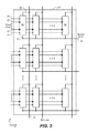
- FIG. 3 illustrates the relation between the source-drain current I D and the control gate voltage V CG for four different charges Q 1 -Q 4 that the floating gate may be selectively storing at any one time at fixed drain voltage.
- FIG. 4 illustrates schematically a string of memory cells organized into a NAND string.
- FIG. 5 illustrates an example of a NAND array 210 of memory cells, constituted from NAND strings 50 such as that shown in FIG. 4 .
- FIG. 6 illustrates a page of memory cells, organized in the NAND configuration, being sensed or programmed in parallel.
- FIGS. 7A-7C illustrate an example of programming a population of memory cells.
- FIGS. 7D-7H illustrate the programming and reading of the 4-state memory encoded with a given 2-bit code.
- FIG. 7I illustrates a foggy-fine programming for an 8-state memory encoded with a given 3-bit code.
- FIG. 8 shows an example of a physical structure of a 3-D NAND string.
- FIGS. 9-12 look at a particular monolithic three dimensional (3D) memory array of the NAND type (more specifically of the “BiCS” type).
- FIG. 13 illustrates the memory being managed by a memory manager with is a software component that resides in the controller.
- FIG. 14 illustrates the software modules of the back-end system.
- FIG. 15A illustrates schematically the mapping between a logical group and a metablock.
- FIG. 15B illustrates schematically the mapping between logical groups and metablocks.
- FIG. 16 illustrates the operation of a memory system in which no new blocks are allocated during a control synchronization.
- FIGS. 17A and 17B illustrate some of the situations that can lead to the loss of data coherency in a memory system that does not block new blocks are allocated during a control synchronization.
- FIG. 18 is a block diagram for an exemplary embodiment of a log structure.
- FIG. 19 provides some detail on block management for a non-blocking control sync system using two free block lists.
- FIGS. 20A-E give examples of free block list content in various saturations.
- FIG. 21 looks at non-blocking control sync operation when two free block lists are used.
- FIG. 1 illustrates schematically the main hardware components of a memory system suitable for implementing the following.
- the memory system 90 typically operates with a host 80 through a host interface.
- the memory system may be in the form of a removable memory such as a memory card, or may be in the form of an embedded memory system.
- the memory system 90 includes a memory 102 whose operations are controlled by a controller 100 .
- the memory 102 comprises one or more array of non-volatile memory cells distributed over one or more integrated circuit chip.
- the controller 100 may include interface circuits 110 , a processor 120 , ROM (read-only-memory) 122 , RAM (random access memory) 130 , programmable nonvolatile memory 124 , and additional components.
- the controller is typically formed as an ASIC (application specific integrated circuit) and the components included in such an ASIC generally depend on the particular application.
- ASIC application specific integrated circuit
- semiconductor memory devices include volatile memory devices, such as dynamic random access memory (“DRAM”) or static random access memory (“SRAM”) devices, non-volatile memory devices, such as resistive random access memory (“ReRAM”), electrically erasable programmable read only memory (“EEPROM”), flash memory (which can also be considered a subset of EEPROM), ferroelectric random access memory (“FRAM”), and magnetoresistive random access memory (“MRAM”), and other semiconductor elements capable of storing information.
- volatile memory devices such as dynamic random access memory (“DRAM”) or static random access memory (“SRAM”) devices
- non-volatile memory devices such as resistive random access memory (“ReRAM”), electrically erasable programmable read only memory (“EEPROM”), flash memory (which can also be considered a subset of EEPROM), ferroelectric random access memory (“FRAM”), and magnetoresistive random access memory (“MRAM”), and other semiconductor elements capable of storing information.
- ReRAM resistive random access memory
- EEPROM electrically erasable programmable
- the memory devices can be formed from passive and/or active elements, in any combinations.
- passive semiconductor memory elements include ReRAM device elements, which in some embodiments include a resistivity switching storage element, such as an anti-fuse, phase change material, etc., and optionally a steering element, such as a diode, etc.
- active semiconductor memory elements include EEPROM and flash memory device elements, which in some embodiments include elements containing a charge storage region, such as a floating gate, conductive nanoparticles, or a charge storage dielectric material.
- Multiple memory elements may be configured so that they are connected in series or so that each element is individually accessible.
- flash memory devices in a NAND configuration typically contain memory elements connected in series.
- a NAND memory array may be configured so that the array is composed of multiple strings of memory in which a string is composed of multiple memory elements sharing a single bit line and accessed as a group.
- memory elements may be configured so that each element is individually accessible, e.g., a NOR memory array.
- NAND and NOR memory configurations are exemplary, and memory elements may be otherwise configured.
- the semiconductor memory elements located within and/or over a substrate may be arranged in two or three dimensions, such as a two dimensional memory structure or a three dimensional memory structure.
- the semiconductor memory elements are arranged in a single plane or a single memory device level.
- memory elements are arranged in a plane (e.g., in an x-z direction plane) which extends substantially parallel to a major surface of a substrate that supports the memory elements.
- the substrate may be a wafer over or in which the layer of the memory elements are formed or it may be a carrier substrate which is attached to the memory elements after they are formed.
- the substrate may include a semiconductor such as silicon.
- the memory elements may be arranged in the single memory device level in an ordered array, such as in a plurality of rows and/or columns. However, the memory elements may be arrayed in non-regular or non-orthogonal configurations.
- the memory elements may each have two or more electrodes or contact lines, such as bit lines and word lines.
- a three dimensional memory array is arranged so that memory elements occupy multiple planes or multiple memory device levels, thereby forming a structure in three dimensions (i.e., in the x, y and z directions, where the y direction is substantially perpendicular and the x and z directions are substantially parallel to the major surface of the substrate).
- a three dimensional memory structure may be vertically arranged as a stack of multiple two dimensional memory device levels.
- a three dimensional memory array may be arranged as multiple vertical columns (e.g., columns extending substantially perpendicular to the major surface of the substrate, i.e., in the y direction) with each column having multiple memory elements in each column.
- the columns may be arranged in a two dimensional configuration, e.g., in an x-z plane, resulting in a three dimensional arrangement of memory elements with elements on multiple vertically stacked memory planes.
- Other configurations of memory elements in three dimensions can also constitute a three dimensional memory array.
- the memory elements may be coupled together to form a NAND string within a single horizontal (e.g., x-z) memory device levels.
- the memory elements may be coupled together to form a vertical NAND string that traverses across multiple horizontal memory device levels.
- Other three dimensional configurations can be envisioned wherein some NAND strings contain memory elements in a single memory level while other strings contain memory elements which span through multiple memory levels.
- Three dimensional memory arrays may also be designed in a NOR configuration and in a ReRAM configuration.
- a monolithic three dimensional memory array typically, one or more memory device levels are formed above a single substrate.
- the monolithic three dimensional memory array may also have one or more memory layers at least partially within the single substrate.
- the substrate may include a semiconductor such as silicon.
- the layers constituting each memory device level of the array are typically formed on the layers of the underlying memory device levels of the array.
- layers of adjacent memory device levels of a monolithic three dimensional memory array may be shared or have intervening layers between memory device levels.
- non-monolithic stacked memories can be constructed by forming memory levels on separate substrates and then stacking the memory levels atop each other. The substrates may be thinned or removed from the memory device levels before stacking, but as the memory device levels are initially formed over separate substrates, the resulting memory arrays are not monolithic three dimensional memory arrays. Further, multiple two dimensional memory arrays or three dimensional memory arrays (monolithic or non-monolithic) may be formed on separate chips and then packaged together to form a stacked-chip memory device.
- Associated circuitry is typically required for operation of the memory elements and for communication with the memory elements.
- memory devices may have circuitry used for controlling and driving memory elements to accomplish functions such as programming and reading.
- This associated circuitry may be on the same substrate as the memory elements and/or on a separate substrate.
- a controller for memory read-write operations may be located on a separate controller chip and/or on the same substrate as the memory elements.
- FIG. 2 illustrates schematically a non-volatile memory cell.
- the memory cell 10 can be implemented by a field-effect transistor having a charge storage unit 20 , such as a floating gate or a charge trapping (dielectric) layer.
- the memory cell 10 also includes a source 14 , a drain 16 , and a control gate 30 .
- non-volatile solid-state memory devices There are many commercially successful non-volatile solid-state memory devices being used today. These memory devices may employ different types of memory cells, each type having one or more charge storage element.
- Typical non-volatile memory cells include EEPROM and flash EEPROM. Also, examples of memory devices utilizing dielectric storage elements.
- the memory state of a cell is usually read by sensing the conduction current across the source and drain electrodes of the cell when a reference voltage is applied to the control gate.
- a corresponding conduction current with respect to a fixed reference control gate voltage may be detected.
- the range of charge programmable onto the floating gate defines a corresponding threshold voltage window or a corresponding conduction current window.
- the threshold voltage for a given memory state under test at the control gate and detect if the conduction current is lower or higher than a threshold current (cell-read reference current).
- the detection of the conduction current relative to a threshold current is accomplished by examining the rate the conduction current is discharging through the capacitance of the bit line.
- FIG. 3 illustrates the relation between the source-drain current I D and the control gate voltage V CG for four different charges Q 1 -Q 4 that the floating gate may be selectively storing at any one time.
- the four solid I D versus V CG curves represent four of seven possible charge levels that can be programmed on a floating gate of a memory cell, respectively corresponding to four possible memory states.
- the threshold voltage window of a population of cells may range from 0.5V to 3.5V. Seven possible programmed memory states “0”, “1”, “2”, “3”, “4”, “5”, “6”, and an erased state (not shown) may be demarcated by partitioning the threshold window into regions in intervals of 0.5V each.
- Q 4 is in a memory state “5”.
- a memory device may have memory cells having a threshold window that ranges from ⁇ 1.5V to 5V. This provides a maximum width of 6.5V. If the memory cell is to store 16 states, each state may occupy from 200 mV to 300 mV in the threshold window. This will require higher precision in programming and reading operations in order to be able to achieve the required resolution.
- FIG. 4 illustrates schematically a string of memory cells organized into a NAND string.
- a pair of select transistors S 1 , S 2 controls the memory transistor chain's connection to the external world via the NAND string's source terminal 54 and drain terminal 56 respectively.
- the source select transistor S 1 when the source select transistor S 1 is turned on, the source terminal is coupled to a source line (see FIG. 5 ).
- the drain select transistor S 2 is turned on, the drain terminal of the NAND string is coupled to a bit line of the memory array.
- Each memory transistor 10 in the chain acts as a memory cell. It has a charge storage element 20 to store a given amount of charge so as to represent an intended memory state.
- a control gate 30 of each memory transistor allows control over read and write operations. As will be seen in FIG. 5 , the control gates 30 of corresponding memory transistors of a row of NAND string are all connected to the same word line. Similarly, a control gate 32 of each of the select transistors S 1 , S 2 provides control access to the NAND string via its source terminal 54 and drain terminal 56 respectively. Likewise, the control gates 32 of corresponding select transistors of a row of NAND string are all connected to the same select line.
- FIG. 5 illustrates an example of a NAND array 210 of memory cells, constituted from NAND strings 50 such as that shown in FIG. 4 .
- a bit line such as bit line 36 is coupled to the drain terminal 56 of each NAND string.
- a source line such as source line 34 is coupled to the source terminals 54 of each NAND string.
- the control gates along a row of memory cells in a bank of NAND strings are connected to a word line such as word line 42 .
- the control gates along a row of select transistors in a bank of NAND strings are connected to a select line such as select line 44 .
- An entire row of memory cells in a bank of NAND strings can be addressed by appropriate voltages on the word lines and select lines of the bank of NAND strings.
- FIG. 6 illustrates a page of memory cells, organized in the NAND configuration, being sensed or programmed in parallel.
- FIG. 6 essentially shows a bank of NAND strings 50 in the memory array 210 of FIG. 5 , where the detail of each NAND string is shown explicitly as in FIG. 4 .
- a physical page such as the page 60 , is a group of memory cells enabled to be sensed or programmed in parallel. This is accomplished by a corresponding page of sense amplifiers 212 . The sensed results are latched in a corresponding set of latches 214 .
- Each sense amplifier can be coupled to a NAND string via a bit line.
- the page is enabled by the control gates of the cells of the page connected in common to a word line 42 and each cell accessible by a sense amplifier accessible via a bit line 36 .
- a sensing voltage or a programming voltage is respectively applied to the common word line WL 3 together with appropriate voltages on the bit lines.
- flash memory differs from other of types of memory. That is the floating gate must first be emptied of charge. Programming then adds a desired amount of charge back to the floating gate. It does not support removing a portion of the charge from the floating gate to go from a more programmed state to a lesser one. This means that updated data cannot overwrite existing data and must be written to a previous unwritten location.
- the array of memory cells is divided into a large number of blocks of memory cells.
- the block is the unit of erase. That is, each block contains the minimum number of memory cells that are erased together. While aggregating a large number of cells in a block to be erased in parallel will improve erase performance, a large size block also entails dealing with a larger number of update and obsolete data.
- Each block is typically divided into a number of physical pages.
- a logical page is a unit of programming or reading that contains a number of bits equal to the number of cells in a physical page.
- one physical page stores one logical page of data.
- a physical page stores two logical pages. The number of logical pages stored in a physical page thus reflects the number of bits stored per cell.
- the individual pages may be divided into segments and the segments may contain the fewest number of cells that are written at one time as a basic programming operation.
- One or more logical pages of data are typically stored in one row of memory cells.
- a page can store one or more sectors.
- a sector includes user data and overhead data.
- FIG. 7A-7C illustrate an example of programming a population of 4-state memory cells.
- FIG. 7A illustrates the population of memory cells programmable into four distinct distributions of threshold voltages respectively representing memory states “0”, “1”, “2” and “3”.
- FIG. 7B illustrates the initial distribution of “erased” threshold voltages for an erased memory.
- FIG. 7C illustrates an example of the memory after many of the memory cells have been programmed. Essentially, a cell initially has an “erased” threshold voltage and programming will move it to a higher value into one of the three zones demarcated by verify levels vV 1 , vV 2 and vV 3 .
- each memory cell can be programmed to one of the three programmed states “1”, “2” and “3” or remain un-programmed in the “erased” state.
- the initial distribution of the “erased” state as shown in FIG. 7B will become narrower and the erased state is represented by the “0” state.
- a 2-bit code having a lower bit and an upper bit can be used to represent each of the four memory states.
- the “0”, “1”, “2” and “3” states are respectively represented by “11”, “01”, “00” and ‘10”.
- the 2-bit data may be read from the memory by sensing in “full-sequence” mode where the two bits are sensed together by sensing relative to the read demarcation threshold values rV 1 , rV 2 and rV 3 in three sub-passes respectively.
- FIGS. 7D-7H illustrate the programming and reading of the 4-state memory encoded with a given 2-bit code.
- FIG. 7D illustrates threshold voltage distributions of the 4-state memory array when each memory cell stores two bits of data using the 2-bit code.
- FIG. 7E illustrates the lower page programming (lower bit) in a 2-pass programming scheme using the 2-bit code.
- the fault-tolerant LM New code essentially avoids any upper page programming to transit through any intermediate states.
- FIG. 7F illustrates the upper page programming (upper bit) in the 2-pass programming scheme using the 2-bit code.
- the logical state (1, 1) transits to (0, 1) as represented by programming the “unprogrammed” memory state “0” to “1”.
- the logical state (0, 0) is obtained by programming from the “intermediate” state to “3”.
- the upper page is to remain at “1”, while the lower page has been programmed to “0”, it will require a transition from the “intermediate” state to (1, 0) as represented by programming the “intermediate” state to “2”.
- FIG. 7G illustrates the read operation that is required to discern the lower bit of the 4-state memory encoded with the 2-bit code.
- a readB operation is first performed to determine if the LM flag can be read. If so, the upper page has been programmed and the readB operation will yield the lower page data correctly. On the other hand, if the upper page has not yet been programmed, the lower page data will be read by a readA operation.
- FIG. 7H illustrates the read operation that is required to discern the upper bit of the 4-state memory encoded with the 2-bit code.
- the upper page read will require a 3-pass read of readA, readB and readC, respectively relative to the demarcation threshold voltages D A , D B and D C .
- a physical page of memory cells will store two logical data pages, a lower data page corresponding to the lower bit and an upper data page corresponding to the upper bit.
- FIG. 7I Another variation on multi-state programming employs a foggy-fine algorithm, as is illustrated in FIG. 7I for a 3-bit memory example. As shown there, this another multi-phase programming operation. A first programming operation is performed as shown in the top line, followed the foggy programming stage. The foggy phase is a full 3-bit programming operation from the first phase using all eight of the final states. At the end of the foggy, though, the data in these states is not yet fully resolved into well defined distributions for each of the 8 states (hence, the “foggy” name) and is not readily extractable.
- FIG. 6 and FIGS. 7A-I illustrate examples of a 2-bit (also referred to as “D 2 ”) memory.
- a D 2 memory has its threshold range or window partitioned into 4 regions, designating 4 states.
- each cell stores 3 bits (low, middle and upper bits) and there are 8 regions.
- D 4 there are 4 bits and 16 regions, etc.
- the memory's finite threshold window is partitioned into more regions, the resolution and for programming and reading will necessarily become finer. Two issues arise as the memory cell is configured to store more bits.
- flash memory has an endurance problem as it ages with use.
- charges is shuttled in and out of the floating gate 20 (see FIG. 2 ) by tunneling across a dielectric. Each time some charges may become trapped in the dielectric and will modify the threshold of the cell. In fact over use, the threshold window will progressively narrow.
- MLC memory generally is designed with tradeoffs between capacity, performance and reliability.
- the memory's threshold window is only partitioned into two regions. This will allow a maximum margin of errors. Thus, binary partitioning while diminished in storage capacity will provide maximum performance and reliability.
- the multi-pass, bit-by-bit programming and reading technique described in connection with FIGS. 7A-I provides a smooth transition between MLC and binary partitioning.
- the memory is programmed with only the lower bit, it is effectively a binary partitioned memory.
- this approach does not fully optimize the range of the threshold window as in the case of a single-level cell (“SLC”) memory, it has the advantage of using the same demarcation or sensing level as in the operations of the lower bit of the MLC memory.
- SLC single-level cell
- the charge programmed into the charge storage element of one memory cell produces an electric field that perturbs the electric field of a neighboring memory cell. This will affect the characteristics of the neighboring memory cell which essentially is a field-effect transistor with a charge storage element. In particular, when sensed the memory cell will appear to have a higher threshold level (or more programmed) than when it is less perturbed.
- the Bit-by-Bit MLC Programming technique described in connection with FIGS. 7A-C above is designed to minimize program disturb from cells along the same word line.
- the thresholds of the cells are moved at most half way up the threshold window. The effect of the first pass is overtaken by the final pass.
- the thresholds are only moved a quarter of the way. In other words, for D 2 , the charge difference among neighboring cells is limited to a quarter of its maximum.
- D 3 with three passes, the final pass will limit the charge difference to one-eighth of its maximum.
- bit-by-bit multi-pass programming technique will be compromised by partial-page programming.
- a page is a group of memory cells, typically along a row or word line, that is programmed together as a unit. It is possible to program non overlapping portions of a page individually over multiple programming passes. However, owning to not all the cells of the page are programmed in a final pass together, it could create large difference in charges programmed among the cells after the page is done. Thus partial-page programming would result in more program disturb and would require a larger margin for sensing accuracy.
- the memory is configured as binary memory
- the margin of operation is wider than that of MLC.
- the binary memory is configured to support partial-page programming in which non-overlapping portions of a page may be programmed individually in one of the multiple programming passes on the page.
- the programming and reading performance can be improved by operating with a page of large size.
- the page size is much larger than the host's unit of write (typically a 512-byte sector)
- its usage will be inefficient. Operating with finer granularity than a page allows more efficient usage of such a page.
- An alternative arrangement to a conventional two-dimensional (2-D) NAND array is a three-dimensional (3-D) array.
- 3-D arrays extend up from the wafer surface and generally include stacks, or columns, of memory cells extending upwards.
- Various 3-D arrangements are possible.
- a NAND string is formed vertically with one end (e.g. source) at the wafer surface and the other end (e.g. drain) on top.
- a NAND string is formed in a U-shape so that both ends of the NAND string are accessible on top, thus facilitating connections between such strings.
- FIG. 8 shows a first example of a NAND string 701 that extends in a vertical direction, i.e. extending in the z-direction, perpendicular to the x-y plane of the substrate.
- Memory cells are formed where a vertical bit line (local bit line) 703 passes through a word line (e.g. WL 0 , WL 1 , etc.).
- a charge trapping layer between the local bit line and the word line stores charge, which affects the threshold voltage of the transistor formed by the word line (gate) coupled to the vertical bit line (channel) that it encircles.
- Such memory cells may be formed by forming stacks of word lines and then etching memory holes where memory cells are to be formed. Memory holes are then lined with a charge trapping layer and filled with a suitable local bit line/channel material (with suitable dielectric layers for isolation).
- select gates 705 , 707 are located at either end of the string to allow the NAND string to be selectively connected to, or isolated from, external elements 709 , 711 .
- external elements are generally conductive lines such as common source lines or bit lines that serve large numbers of NAND strings.
- Vertical NAND strings may be operated in a similar manner to planar NAND strings and both SLC and MLC operation is possible. While FIG. 8 shows an example of a NAND string that has 32 cells (0-31) connected in series, the number of cells in a NAND string may be any suitable number. Not all cells are shown for clarity. It will be understood that additional cells are formed where word lines 3-29 (not shown) intersect the local vertical bit line.
- a 3D NAND array can, loosely speaking, be formed tilting up the respective structures 50 and 210 of FIGS. 5 and 6 to be perpendicular to the x-y plane.
- each y-z plane corresponds to the page structure of FIG. 6 , with m such plane at differing x locations.
- the (global) bit lines, BL 1 - m each run across the top to an associated sense amp SA 1 - m .
- the word lines, WL 1 - n , and source and select lines SSL 1 - n and DSL 1 - n then run in x direction, with the NAND string connected at bottom to a common source line CSL.
- FIGS. 9-12 look at a particular monolithic three dimensional (3D) memory array of the NAND type (more specifically of the “BiCS” type), where one or more memory device levels are formed above a single substrate, in more detail.
- FIG. 9 is an oblique projection of part of such a structure, showing a portion corresponding to two of the page structures in FIG. 5 , where, depending on the embodiment, each of these could correspond to a separate block or be different “fingers” of the same block.
- the NAND strings lying in a common y-z plane they are squashed together in the y direction, so that the NAND strings are somewhat staggered in the x direction.
- the NAND strings are connected along global bit lines (BL) spanning multiple such sub-divisions of the array that run in the x direction.
- global common source lines also run across multiple such structures in the x direction and are connect to the sources at the bottoms of the NAND string, which are connected by a local interconnect (LI) that serves as the local common source line of the individual finger.
- LI local interconnect
- the global source lines can span the whole, or just a portion, of the array structure.
- variations can include the NAND string being formed in a U type structure, where part of the string itself runs back up.
- FIG. 9 To the right of FIG. 9 is a representation of the elements of one of the vertical NAND strings from the structure to the left.
- Multiple memory cells are connected through a drain select gate SGD to the associated bit line BL at the top and connected through the associated source select gate SDS to the associated local source line LI to a global source line SL.
- SGD Drain select gate
- SDS Source select gate
- the select gates are programmable to have their threshold levels adjusted.
- This exemplary embodiment also includes several dummy cells at the ends that are not used to store user data, as their proximity to the select gates makes them more prone to disturbs.
- FIG. 10 shows a top view of the structure for two blocks in the exemplary embodiment.
- Two blocks (BLK 0 above, BLK 1 below) are shown, each having four fingers that run left to right.
- the word lines and select gate lines of each level also run left to right, with the word lines of the different fingers of the same block being commonly connected at a “terrace” and then on to receive their various voltage level through the word line select gates at WLTr.
- the word lines of a given layer in a block can also be commonly connected on the far side from the terrace.
- the selected gate lines can be individual for each level, rather common, allowing the fingers to be individually selected.
- the bit lines are shown running up and down the page and connect on to the sense amp circuits, where, depending on the embodiment, each sense amp can correspond to a single bit line or be multiplexed to several bit lines.
- FIG. 11 shows a side view of one block, again with four fingers.
- the select gates SGD and SGS at either end of the NAND strings are formed of four layers, with the word lines WL in-between, all formed over a CPWELL.
- a given finger is selected by setting its select gates to a level VSG and the word lines are biased according to the operation, such as a read voltage (VCGRV) for the selected word lines and the read-pass voltage (VREAD) for the non-selected word lines.
- the non-selected fingers can then be cut off by setting their select gates accordingly.
- FIG. 12 illustrates some detail of an individual cell.
- a dielectric core runs in the vertical direction and is surrounded by a channel silicon layer, that is in turn surrounded a tunnel dielectric (TNL) and then the charge trapping dielectric layer (CTL).
- TNL tunnel dielectric
- CTL charge trapping dielectric layer
- the gate of the cell is here formed of tungsten with which is surrounded by a metal barrier and is separated from the charge trapping layer by blocking (BLK) oxide and a high K layer.
- BLK blocking
- FIG. 13 illustrates the memory being managed by a memory manager which is a software component that resides in the controller.
- the memory 200 is organized into blocks, each block of cells being a minimum unit of erase.
- the memory system may operate with even large units of erase formed by an aggregate of blocks into “metablocks” and also “megablocks”.
- a unit of erase as a metablock although it will be understood that some systems operate with even larger unit of erase such as a “megablock” formed by an aggregate of metablocks.
- the host 80 accesses the memory 200 when running an application under a file system or operating system.
- the host system addresses data in units of logical sectors where, for example, each sector may contain 512 bytes of data.
- an optional host-side memory manager may exist to perform lower level memory management at the host.
- the host 80 In most cases during read or write operations, the host 80 essentially issues a command to the memory system 90 to read or write a segment containing a string of logical sectors of data with contiguous addresses.
- a memory-side memory manager 300 is implemented in the controller 100 of the memory system 90 to manage the storage and retrieval of the data of host logical sectors among metablocks of the flash memory 200 .
- the memory manager comprises a front-end system 310 and a back-end system 320 .
- the front-end system 310 includes a host interface 312 .
- the back-end system 320 includes a number of software modules for managing erase, read and write operations of the metablocks.
- the memory manager also maintains system control data and directory data associated with its operations among the flash memory 200 and the controller RAM 130 .
- FIG. 14 illustrates the software modules of the back-end system.
- the Back-End System mainly comprises two functional modules: a Media Management Layer 330 and a Dataflow and Sequencing Layer 340 .
- the dataflow and sequencing layer 340 is responsible for the sequencing and transfer of sectors of data between a front-end system and a flash memory.
- This layer includes a command sequencer 342 , a low-level sequencer 344 and a flash Control layer 346 .
- the memory manager 300 is preferably implemented in the controller 100 . It translates logical addresses received from the host into physical addresses within the memory array, where the data are actually stored, and then keeps track of these address translations.
- FIG. 15A illustrates schematically the logical to physical mapping in a metablock level arrangement, where the mapping is between a logical group and a metablock.
- the metablock of the physical memory has N physical sectors for storing N logical sectors of data of a logical group.
- FIG. 15A at top shows the data from a logical group LG i , where the logical sectors are in contiguous logical order 0, 1, . . . , N ⁇ 1.
- FIG. 15A in the middle row shows the same data being stored in the metablock in the same logical order.
- the metablock when stored in this manner is said to be “sequential.”
- the metablock may have data stored in a different order, in which case the metablock is said to be “non-sequential” or “chaotic.”
- logical sector address wraps round as a loop from bottom back to top of the logical group within the metablock.
- the metablock stores in its first location beginning with the data of logical sector k.
- the last logical sector N ⁇ 1 wraps around to sector 0 and finally storing data associated with logical sector k ⁇ 1 in its last physical sector.
- a page tag is used to identify any offset, such as identifying the starting logical sector address of the data stored in the first physical sector of the metablock. Two blocks will be considered to have their logical sectors stored in similar order when they only differ by a page tag.
- FIG. 15B illustrates schematically the mapping between logical groups and metablocks.
- Each logical group 380 is mapped to a unique metablock 370 , except for a small number of logical groups in which data is currently being updated. After a logical group has been updated, it may be mapped to a different metablock.
- the mapping information is maintained in a set of logical to physical directories, which will be described in more detail later.
- the management tables are stored in the flash memory, but in order to provide high performance management table copies are also maintained in the controller RAM, typically a DRAM.
- the updated tables are stored in the memory section from time to time for synchronization in a Control Sync (CS) operation, involving the sub-operations of preparing for the CS, submitting a request to write a “log” of the operation, and receiving confirmation that the entire “log” was written successfully.
- CS Control Sync
- FIG. 16 schematically represents such a blocking control sync operation, where any new read or write operations are blocked until the previously allocated operations in dies A, B, and C are complete and a ready signal is returned.
- the blocking arrangement allows for the memory system to maintain coherency of the memory system's logical to physical assignments, the blocking of operations affects performance.
- This section presents techniques whereby the controller can allocate new blocks and maintain data to control information coherency in a non-blocking control sync system by using two free block lists prepared with different timings. More specifically, block allocation is performed from a first free block list (FBL) that the controller compiles of available blocks until the controller gets a completion notification that the RAM log was synced to flash, and then allocation switches to a second FBL. Both FBLs are stored in controller RAM and in the flash, and the second FBL is created by the controller when a new control sync starts.
- FBL free block list
- an FBL assembled from this pool can have advantages. For example, in case of an unplanned shut down (an ungraceful shutdown, or UGSD), the system will need to restore all the blocks that were allocated since last control-syn, in order to restore the data. Restoring block allocations typically involves reading some metadata from all blocks that are candidates for allocation, which can be an involved process.
- an FBL list which is a short list of blocks that are candidates for allocation
- the system will only need scan the blocks from the FBL. In the case of 2 FBLs, the system will scan both lists. During mount to restore allocations that were done during control-sync and also allocation that were done after control-sync was done. With two FBLs, this allows for one list to be used during the control-sync itself and another to be used after control-sync is done.
- the compiling of the free block lists, and allocation of blocks from an active FBL can be performed similarly to how this is done in systems using a FBL, such is describe in US patent publication number 2012-0191927, for example.
- New blocks can be added to an FBL from a pool of available blocks that can contain previously unwritten blocks as well as previously written blocks that have been released.
- a block is released when it no longer contains valid data, for example, and placed in the pool of available blocks either after or before being erased, depending on the embodiment.
- the selection of a block for a FBL from the pool of available blocks can be based various criteria, including considerations such as wear leveling, the number of program-erase (P/E) cycles a block has experienced, previous occurrences of error in a block and so on.
- P/E program-erase
- blocks may also be removed in order to be replaced with “better” blocks from the available pool, again based block characteristics such as wear leveling, the number of program-erase (P/E) cycles a block has experienced, previous occurrences of error in a block and so on.
- block characteristics such as wear leveling, the number of program-erase (P/E) cycles a block has experienced, previous occurrences of error in a block and so on.
- Block allocation in a non-blocking control sync flash transfer layer (FTL) system may be provided by allocating and managing blocks from two free block lists (FBLs) stored in the controller RAM, where a copy of the two FBLs will be stored also in the flash memory and updated every time a non-blocking CS operation is performed.
- the FTL can be implemented as a firmware module on the controller, such as part of the memory management layer 330 of FIG. 14 .
- FIGS. 17A and 17B can be used to illustrate non-blocking operation and the sort of problem that may occur in a non-blocking CS with only a single FBL.
- FIGS. 17A and 17B illustrate a non-blocking arrangement using only a single free block list and are arranged similarly to FIG. 16 , beginning with the trigger for next control sync and the preparation of a new log and free block list in the controller.
- FIG. 16 as operations on the different previously allocated dies complete, (here on dies A, B, and C), they indicate their ready status.
- new blocks can be allocated from the previously assembled free block list in response to new commands, allowing for increased performance.
- FIG. 17A illustrates the situation where, during the control-sync operation, the system is still allocating blocks from the old FBL as held in controller RAM.
- UGSD ungraceful shutdown
- FIG. 17B illustrates the situation in which the system is allocating blocks from the newly prepared FBL during control-sync operation and a UGSD occurs after the trigger for the next control sync and before writing the log to non-volatile memory.
- blocks that the system has allocated from the new FBL may be lost due to a UGSD in the time window represented by the ellipse.
- the correct time for the FTL to start allocating blocks from the new FBL is when “write log to flash” happens; however, the FTL layer is not aware of the timing of “write log to flash”, but only of the “trigger for next control sync” and “write log confirmation”.
- the preparation of an updated FBL includes adding new blocks released by memory management operations (such as garbage collection relocations) and removal of blocks from the FBL that were already allocated.
- a new command allocation from the FBL that occurs after the new updated log was prepared and written to flash will be updated in the controller's RAM tables, but may be lost due to an ungraceful shutdown (UGSD) since after mount (copying of the FBL as stored in non-volatile memory to the controller RAM) the recovery will be made according to the stored log (with ambiguity if it is the updated log or the old log copy). Consequently, the newly allocated block may not be recovered from the new FBL read from flash in case it is the updated FBL that does not include the block allocation performed after it was prepared as shown in FIGS. 17A and 17B .
- UGSD ungraceful shutdown
- an exemplary embodiment uses two FBLs: a first FBL that includes a list of allocated blocks prior to the current non-blocking CS preparation start; and a second list includes an updated block list that includes blocks that were added or removed as part of the preparations for the next CS. Both FBLs will be written to the log and the flash in the non-blocking CS. In case of mount after an ungraceful shutdown, the two FBLs can be read from the memory section and scanned in order to recover the control information in controller RAM and allowing continuous operation with non-blocking control syncs.
- FIG. 18 is a schematic representation for an example of a log structure 501 , containing the two free block lists FBL #1 503 and FBL #2 505 .
- the log structure can also include mapping tables information 507 for logical to physical translation, block information 509 (such as experience counts (i.e. program/erase cycles) or measures of block quality, such as errors or defects), a pool of open blocks 511 that are available for the free block lists, and other information 513 .
- Other examples of block and other information can include: statistics counters, a state of each block (allocated/free/reserved-for-exceptions/etc. . . . ), type of block (binary, multistate), list of read-scrub blocks (blocks with high bit error rates), information about additional control blocks in the system, and so on.
- One exemplary embodiment of a block allocating method can be as follows: when a non-blocking CS operation is prepared by the controller, a new or updated FBL, here labelled FBL#3, is created to replace the previous FBL#1, as illustrated in FIG. 19 .
- the timing diagram of FIG. 19 illustrates the creation of a new FBL, which blocks will be scanned after UGSD and from which new blocks will be allocated from a first FBL (FBL #2) while the newly created FBL (FBL #3) will not be used for block allocations until the control sync ends and a completion is received.
- the top row shows the flow for a control sync operation; the second row illustrate the FBLs from which blocks are scanned after an UGSD; and the bottom row shows the FBL from which blocks are allocated.
- new blocks will be allocated from FBL#2 before a log write confirmation is received from the die(s), and new block allocations will be made from FBL#3 only after receiving the log write confirmation.
- the ellipse illustrates the time during the control sync when new block allocations would have otherwise been blocked in a blocking arrangement.
- FIG. 20B looks at block allocation during a control sync.
- blocks have been allocated from FBL #2 (Block ID 12 , Block ID 17 ), but these are not removed from FBL #3 during the control sync after these have been prepared.
- new blocks here Block ID 15 , Block ID 85 .
- FIG. 20C shows allocation after control sync. As FBL #2 is prepared, then some blocks can be allocated out of FBL #2 (Block ID 12 and Block ID 17 ), with others blocks of FBL #2 left as unassigned remainders. The preparation of FBL #3 can start from the remainders of FBL #2, but blocks can be removed from the list and other blocks may be added to the list.
- FIG. 20C illustrates Bocks ID 17 and ID 101 being allocated from FBL #3.
- FIG. 20D looks at mount after an ungraceful shut down, but before control sync completion.
- the log with the two FBLs FBL #1 and FBL #2
- the management tables can be restored accordingly, including identifying blocks that were allocated after the last control sync and not removed from the FBL and control-to-data coherency is maintained.
- FIG. 20E looks at mount after an ungraceful shut down and after control sync completion.
- the log with the updated FBLs FBL #2 and FBL #3
- the management table can be restored accord to the scan, including identifying blocks that were allocated after the last control sync and not removed from the FBL and control-to-data coherency is again maintained.
- the two FBLs can be read from flash and scanned to recover the control data in the volatile memory used by the controller.
- the two FBLs can be FBL#1 and FBL#2 if the log write request was not written to non-volatile memory before the UGSD and the log write completion note was not received; or FBL#2 and FBL#3 if the log write request was completed.
- the FTL can see that data to control information is coherent and not lost.
- blocks may be allocated from the FBL#2 stored in the controller's RAM, and a smaller list FBL#2′ (not shown in the figures) can be updated in the RAM having smaller number of blocks comparing to the original FBL#2.
- the controller can write in the block's metadata an indication that this is new data. For example, this could be written in the first physical page, or smallest read unit, of the block.
- the controller can read the metadata of the first read unit of each of the blocks in the two FBL lists and determine if the block was allocated and re-written or not. In this way the system can restore which blocks were allocated since the last control sync operation. Blocks that appeared in FBL#2, but were allocated during the CS operation and do not appear anymore in FBL#2′, can still be found and restored in the RAM control tables during mount since they can be read from the control data stored in the non-volatile memory. As shown in FIG. 21 , new block allocation from FBL#2 that will not be seen in the FBLs stored on flash after a UGSD.
- FIG. 21 further illustrates the exemplary non-blocking control sync with two FBLs, beginning with the trigger for the control sync and the preparation of the new FBL #3.
- previously allocated operations complete and return a ready status.
- new command block allocations Prior to writing the log to non-volatile memory for FBL #2 and FBL #3, new command block allocations are made from FBL #2. After writing the log, but before confirmation, allocations are still made from FBL #2. After confirmation, new command block allocations are made from FBL #3.
- the use of two free block lists for block allocation allows for non-blocking control sync, while providing coherent flash transfer layer operation without losing control information in the case of an ungraceful shut down.
- the non-blocking operation improves performance by allowing the system to operate continuously by not halting multi flash die read/write operations during control sync operations.
Abstract
In a non-volatile memory system, the controller maintains in its volatile memory two free block lists for the assignment of memory circuit blocks when writing user and system data. Copies of the free block lists are maintained in the non-volatile memory. While allocating blocks from a first of the free block lists, the controller can update a second of the free block lists as part of a control sync operation preparing control data stored in non-volatile memory. This allows the memory system to operate in a non-blocking manner during the control sync. Once the second free block lists is prepared and the control sync completed, the second block can subsequently be used for block allocations and a control sync operation can be done to update the first block.
Description
The following relates to the operation of re-programmable non-volatile memory systems, such as semiconductor flash memory, and the management of such systems.
Solid-state memory capable of nonvolatile storage of charge, particularly in the form of EEPROM and flash EEPROM packaged as a small form factor card, has recently become the storage of choice in a variety of mobile and handheld devices, notably information appliances and consumer electronics products. Unlike RAM (random access memory) that is also solid-state memory, flash memory is non-volatile, and retains its stored data even after power is turned off. Also, unlike ROM (read only memory), flash memory is rewritable similar to a disk storage device. In spite of the higher cost, flash memory is increasingly being used in mass storage applications.
Flash EEPROM is similar to EEPROM (electrically erasable and programmable read-only memory) in that it is a non-volatile memory that can be erased and have new data written or “programmed” into their memory cells. Both utilize a floating (unconnected) conductive gate, in a field effect transistor structure, positioned over a channel region in a semiconductor substrate, between source and drain regions. A control gate is then provided over the floating gate. The threshold voltage characteristic of the transistor is controlled by the amount of charge that is retained on the floating gate. That is, for a given level of charge on the floating gate, there is a corresponding voltage (threshold) that must be applied to the control gate before the transistor is turned “on” to permit conduction between its source and drain regions. Flash memory such as Flash EEPROM allows entire blocks of memory cells to be erased at the same time.
The floating gate can hold a range of charges and therefore can be programmed to any threshold voltage level within a threshold voltage window. The size of the threshold voltage window is delimited by the minimum and maximum threshold levels of the device, which in turn correspond to the range of the charges that can be programmed onto the floating gate. The threshold window generally depends on the memory device's characteristics, operating conditions and history. Each distinct, resolvable threshold voltage level range within the window may, in principle, be used to designate a definite memory state of the cell.
In order to improve read and program performance, multiple charge storage elements or memory transistors in an array are read or programmed in parallel. Thus, a “page” of memory elements are read or programmed together. In existing memory architectures, a row typically contains several interleaved pages or it may constitute one page. All memory elements of a page are read or programmed together.
Nonvolatile memory devices are also manufactured from memory cells with a dielectric layer for storing charge. Instead of the conductive floating gate elements described earlier, a dielectric layer is used. An ONO dielectric layer extends across the channel between source and drain diffusions. The charge for one data bit is localized in the dielectric layer adjacent to the drain, and the charge for the other data bit is localized in the dielectric layer adjacent to the source. For example, a nonvolatile memory cell may have a trapping dielectric sandwiched between two silicon dioxide layers. Multi-state data storage is implemented by separately reading the binary states of the spatially separated charge storage regions within the dielectric.
Non-volatile memory storage devices typically include a controller portion and a memory section and used a use logical-to-physical (L2P) mapping and use management tables for dynamic mapping. The logical-to physical mapping is performed by the controller and associates a physical address on the memory section where data is stored with a logical address by which a host identifies the data. In a standard arrangement, the management tables are stored in the non-volatile memory, but in order to provide high performance, management table copies are maintained also in the controller RAM, typically a DRAM. As the controller updates these tables during memory operations, the updated tables stored in the non-volatile device from time to time for synchronization, in an operation called Control Sync (CS).
If the system experiences an ungraceful shutdown (UGSD), such as losing power, any information updates made since the last control sync is lost, as this information was only held in volatile control memory. To avoid this problem, the system can operate in a blocking manner, where the flash controller does not send read/write commands to the flash dies, allowing them to complete their workload. Only after the workload is completed, confirmed and the control data is updated in the log are a new set of read/write commands sent. As the new block allocation will be performed according to the new log, data to control info coherency can be maintained, but at a loss of system performance due to the blocking.
In a method of operating a non-volatile memory system, data is stored in a non-volatile memory circuit having a plurality of non-volatile memory cells formed as a plurality of multi-cell blocks and a controller manages the storage of data on the memory circuit. The managing includes maintaining in volatile memory of two or more free block lists, the block lists being formed of blocks available for the writing of data, and maintaining copies of the free block lists in the non-volatile memory. Blocks are allocated from a first of the free block lists, and, while allocating blocks from the first free block list, performing a synchronizing operation is performed for a second of the free block lists. The synchronizing operation includes updating the second free block list and preparing control data related to the updating of the second free block list.
In other aspects, a controller for a non-volatile memory system includes a volatile memory and logic circuitry configured to manage the storage of data on a non-volatile memory circuit having a plurality of non-volatile memory cells formed as a plurality of multi-cell blocks. Managing the storage of data on the non-volatile memory circuit includes: maintaining in the volatile memory of two or more free block lists, the block lists being formed of blocks available for the writing of data, and maintaining copies of the free block lists in the non-volatile memory. Blocks are allocated from a first of the free block lists, and, while allocating blocks from the first free block list, performing a synchronizing operation is performed for a second of the free block lists. The synchronizing operation includes updating the second free block list and preparing control data related to the updating of the second free block list.
In further aspects, a non-volatile memory system includes a non-volatile memory circuit having a plurality of non-volatile memory cells formed as a plurality of multi-cell blocks and a controller. The controller includes a volatile memory and logic circuitry configured to manage the storage of data on the non-volatile memory circuit. Managing the storage of data on the non-volatile memory circuit includes: maintaining in the volatile memory of two or more free block lists, the block lists being formed of blocks available for the writing of data, and maintaining copies of the free block lists in the non-volatile memory. Blocks are allocated from a first of the free block lists, and, while allocating blocks from the first free block list, performing a synchronizing operation is performed for a second of the free block lists. The synchronizing operation includes updating the second free block list and preparing control data related to the updating of the second free block list.
Various aspects, advantages, features and embodiments are included in the following description of exemplary examples thereof, which description should be taken in conjunction with the accompanying drawings. All patents, patent applications, articles, other publications, documents and things referenced herein are hereby incorporated herein by this reference in their entirety for all purposes. To the extent of any inconsistency or conflict in the definition or use of terms between any of the incorporated publications, documents or things and the present application, those of the present application shall prevail.
Memory System
With respect to the memory section 102, semiconductor memory devices include volatile memory devices, such as dynamic random access memory (“DRAM”) or static random access memory (“SRAM”) devices, non-volatile memory devices, such as resistive random access memory (“ReRAM”), electrically erasable programmable read only memory (“EEPROM”), flash memory (which can also be considered a subset of EEPROM), ferroelectric random access memory (“FRAM”), and magnetoresistive random access memory (“MRAM”), and other semiconductor elements capable of storing information. Each type of memory device may have different configurations. For example, flash memory devices may be configured in a NAND or a NOR configuration.
The memory devices can be formed from passive and/or active elements, in any combinations. By way of non-limiting example, passive semiconductor memory elements include ReRAM device elements, which in some embodiments include a resistivity switching storage element, such as an anti-fuse, phase change material, etc., and optionally a steering element, such as a diode, etc. Further by way of non-limiting example, active semiconductor memory elements include EEPROM and flash memory device elements, which in some embodiments include elements containing a charge storage region, such as a floating gate, conductive nanoparticles, or a charge storage dielectric material.
Multiple memory elements may be configured so that they are connected in series or so that each element is individually accessible. By way of non-limiting example, flash memory devices in a NAND configuration (NAND memory) typically contain memory elements connected in series. A NAND memory array may be configured so that the array is composed of multiple strings of memory in which a string is composed of multiple memory elements sharing a single bit line and accessed as a group. Alternatively, memory elements may be configured so that each element is individually accessible, e.g., a NOR memory array. NAND and NOR memory configurations are exemplary, and memory elements may be otherwise configured.
The semiconductor memory elements located within and/or over a substrate may be arranged in two or three dimensions, such as a two dimensional memory structure or a three dimensional memory structure.
In a two dimensional memory structure, the semiconductor memory elements are arranged in a single plane or a single memory device level. Typically, in a two dimensional memory structure, memory elements are arranged in a plane (e.g., in an x-z direction plane) which extends substantially parallel to a major surface of a substrate that supports the memory elements. The substrate may be a wafer over or in which the layer of the memory elements are formed or it may be a carrier substrate which is attached to the memory elements after they are formed. As a non-limiting example, the substrate may include a semiconductor such as silicon.
The memory elements may be arranged in the single memory device level in an ordered array, such as in a plurality of rows and/or columns. However, the memory elements may be arrayed in non-regular or non-orthogonal configurations. The memory elements may each have two or more electrodes or contact lines, such as bit lines and word lines.
A three dimensional memory array is arranged so that memory elements occupy multiple planes or multiple memory device levels, thereby forming a structure in three dimensions (i.e., in the x, y and z directions, where the y direction is substantially perpendicular and the x and z directions are substantially parallel to the major surface of the substrate).
As a non-limiting example, a three dimensional memory structure may be vertically arranged as a stack of multiple two dimensional memory device levels. As another non-limiting example, a three dimensional memory array may be arranged as multiple vertical columns (e.g., columns extending substantially perpendicular to the major surface of the substrate, i.e., in the y direction) with each column having multiple memory elements in each column. The columns may be arranged in a two dimensional configuration, e.g., in an x-z plane, resulting in a three dimensional arrangement of memory elements with elements on multiple vertically stacked memory planes. Other configurations of memory elements in three dimensions can also constitute a three dimensional memory array.
By way of non-limiting example, in a three dimensional NAND memory array, the memory elements may be coupled together to form a NAND string within a single horizontal (e.g., x-z) memory device levels. Alternatively, the memory elements may be coupled together to form a vertical NAND string that traverses across multiple horizontal memory device levels. Other three dimensional configurations can be envisioned wherein some NAND strings contain memory elements in a single memory level while other strings contain memory elements which span through multiple memory levels. Three dimensional memory arrays may also be designed in a NOR configuration and in a ReRAM configuration.
Typically, in a monolithic three dimensional memory array, one or more memory device levels are formed above a single substrate. Optionally, the monolithic three dimensional memory array may also have one or more memory layers at least partially within the single substrate. As a non-limiting example, the substrate may include a semiconductor such as silicon. In a monolithic three dimensional array, the layers constituting each memory device level of the array are typically formed on the layers of the underlying memory device levels of the array. However, layers of adjacent memory device levels of a monolithic three dimensional memory array may be shared or have intervening layers between memory device levels.
Then again, two dimensional arrays may be formed separately and then packaged together to form a non-monolithic memory device having multiple layers of memory. For example, non-monolithic stacked memories can be constructed by forming memory levels on separate substrates and then stacking the memory levels atop each other. The substrates may be thinned or removed from the memory device levels before stacking, but as the memory device levels are initially formed over separate substrates, the resulting memory arrays are not monolithic three dimensional memory arrays. Further, multiple two dimensional memory arrays or three dimensional memory arrays (monolithic or non-monolithic) may be formed on separate chips and then packaged together to form a stacked-chip memory device.
Associated circuitry is typically required for operation of the memory elements and for communication with the memory elements. As non-limiting examples, memory devices may have circuitry used for controlling and driving memory elements to accomplish functions such as programming and reading. This associated circuitry may be on the same substrate as the memory elements and/or on a separate substrate. For example, a controller for memory read-write operations may be located on a separate controller chip and/or on the same substrate as the memory elements.
It will be recognized that the following is not limited to the two dimensional and three dimensional exemplary structures described but cover all relevant memory structures within the spirit and scope as described herein
Physical Memory Structure
There are many commercially successful non-volatile solid-state memory devices being used today. These memory devices may employ different types of memory cells, each type having one or more charge storage element.
Typical non-volatile memory cells include EEPROM and flash EEPROM. Also, examples of memory devices utilizing dielectric storage elements.
In practice, the memory state of a cell is usually read by sensing the conduction current across the source and drain electrodes of the cell when a reference voltage is applied to the control gate. Thus, for each given charge on the floating gate of a cell, a corresponding conduction current with respect to a fixed reference control gate voltage may be detected. Similarly, the range of charge programmable onto the floating gate defines a corresponding threshold voltage window or a corresponding conduction current window.
Alternatively, instead of detecting the conduction current among a partitioned current window, it is possible to set the threshold voltage for a given memory state under test at the control gate and detect if the conduction current is lower or higher than a threshold current (cell-read reference current). In one implementation the detection of the conduction current relative to a threshold current is accomplished by examining the rate the conduction current is discharging through the capacitance of the bit line.
As can be seen from the description above, the more states a memory cell is made to store, the more finely divided is its threshold window. For example, a memory device may have memory cells having a threshold window that ranges from −1.5V to 5V. This provides a maximum width of 6.5V. If the memory cell is to store 16 states, each state may occupy from 200 mV to 300 mV in the threshold window. This will require higher precision in programming and reading operations in order to be able to achieve the required resolution.
NAND Structure
When an addressed memory transistor 10 within a NAND string is read or is verified during programming, its control gate 30 is supplied with an appropriate voltage. At the same time, the rest of the non-addressed memory transistors in the NAND string 50 are fully turned on by application of sufficient voltage on their control gates. In this way, a conductive path is effectively created from the source of the individual memory transistor to the source terminal 54 of the NAND string and likewise for the drain of the individual memory transistor to the drain terminal 56 of the cell.
Physical Organization of the Memory
One difference between flash memory and other of types of memory is that a cell must be programmed from the erased state. That is the floating gate must first be emptied of charge. Programming then adds a desired amount of charge back to the floating gate. It does not support removing a portion of the charge from the floating gate to go from a more programmed state to a lesser one. This means that updated data cannot overwrite existing data and must be written to a previous unwritten location.
Furthermore erasing is to empty all the charges from the floating gate and generally takes appreciable time. For that reason, it will be cumbersome and very slow to erase cell by cell or even page by page. In practice, the array of memory cells is divided into a large number of blocks of memory cells. As is common for flash EEPROM systems, the block is the unit of erase. That is, each block contains the minimum number of memory cells that are erased together. While aggregating a large number of cells in a block to be erased in parallel will improve erase performance, a large size block also entails dealing with a larger number of update and obsolete data.
Each block is typically divided into a number of physical pages. A logical page is a unit of programming or reading that contains a number of bits equal to the number of cells in a physical page. In a memory that stores one bit per cell, one physical page stores one logical page of data. In memories that store two bits per cell, a physical page stores two logical pages. The number of logical pages stored in a physical page thus reflects the number of bits stored per cell. In one embodiment, the individual pages may be divided into segments and the segments may contain the fewest number of cells that are written at one time as a basic programming operation. One or more logical pages of data are typically stored in one row of memory cells. A page can store one or more sectors. A sector includes user data and overhead data.
All-Bit, Full-Sequence MLC Programming
A 2-bit code having a lower bit and an upper bit can be used to represent each of the four memory states. For example, the “0”, “1”, “2” and “3” states are respectively represented by “11”, “01”, “00” and ‘10”. The 2-bit data may be read from the memory by sensing in “full-sequence” mode where the two bits are sensed together by sensing relative to the read demarcation threshold values rV1, rV2 and rV3 in three sub-passes respectively.
Bit-by-Bit MLC Programming and Reading
In the bit-by-bit scheme for a 2-bit memory, a physical page of memory cells will store two logical data pages, a lower data page corresponding to the lower bit and an upper data page corresponding to the upper bit.
Foggy-Fine Programming
Another variation on multi-state programming employs a foggy-fine algorithm, as is illustrated in FIG. 7I for a 3-bit memory example. As shown there, this another multi-phase programming operation. A first programming operation is performed as shown in the top line, followed the foggy programming stage. The foggy phase is a full 3-bit programming operation from the first phase using all eight of the final states. At the end of the foggy, though, the data in these states is not yet fully resolved into well defined distributions for each of the 8 states (hence, the “foggy” name) and is not readily extractable.
As each cell is, however, programmed to near its eventual target state, the sort of neighboring cell to cell couplings, or “Yupin” effect, described in U.S. Pat. No. 6,870,768 are presenting most of their effect. Because of this, when the fine program phase (shown on the bottom line) is executed, these couplings have largely been factored in to this final phase so the cell distributions are more accurately resolved to their target ranges.
Binary and MLC Memory Partitioning
First, programming or reading will be slower when the threshold of a cell must be more accurately programmed or read. In fact in practice the sensing time (needed in programming and reading) tends to increase as the square of the number of partitioning levels.
Secondly, flash memory has an endurance problem as it ages with use. When a cell is repeatedly programmed and erased, charges is shuttled in and out of the floating gate 20 (see FIG. 2 ) by tunneling across a dielectric. Each time some charges may become trapped in the dielectric and will modify the threshold of the cell. In fact over use, the threshold window will progressively narrow. Thus, MLC memory generally is designed with tradeoffs between capacity, performance and reliability.
Conversely, it will be seen for a binary memory, the memory's threshold window is only partitioned into two regions. This will allow a maximum margin of errors. Thus, binary partitioning while diminished in storage capacity will provide maximum performance and reliability.
The multi-pass, bit-by-bit programming and reading technique described in connection with FIGS. 7A-I provides a smooth transition between MLC and binary partitioning. In this case, if the memory is programmed with only the lower bit, it is effectively a binary partitioned memory. While this approach does not fully optimize the range of the threshold window as in the case of a single-level cell (“SLC”) memory, it has the advantage of using the same demarcation or sensing level as in the operations of the lower bit of the MLC memory. As will be described later, this approach allows a MLC memory to be “expropriated” for use as a binary memory, or vice versa. How it should be understood that MLC memory tends to have more stringent specification for usage.
Binary Memory and Partial Page Programming
The charge programmed into the charge storage element of one memory cell produces an electric field that perturbs the electric field of a neighboring memory cell. This will affect the characteristics of the neighboring memory cell which essentially is a field-effect transistor with a charge storage element. In particular, when sensed the memory cell will appear to have a higher threshold level (or more programmed) than when it is less perturbed.
In general, if a memory cell is program-verified under a first field environment and later is read again under a different field environment due to neighboring cells subsequently being programmed with different charges, the read accuracy may be affected due to coupling between neighboring floating gates in what is referred to as the “Yupin Effect”. With ever higher integration in semiconductor memories, the perturbation of the electric field due to the stored charges between memory cells (Yupin effect) becomes increasing appreciable as the inter-cellular spacing shrinks.
The Bit-by-Bit MLC Programming technique described in connection with FIGS. 7A-C above is designed to minimize program disturb from cells along the same word line. As can be seen from FIG. 7D , in a first of the two programming passes, the thresholds of the cells are moved at most half way up the threshold window. The effect of the first pass is overtaken by the final pass. In the final pass, the thresholds are only moved a quarter of the way. In other words, for D2, the charge difference among neighboring cells is limited to a quarter of its maximum. For D3, with three passes, the final pass will limit the charge difference to one-eighth of its maximum.
However, the bit-by-bit multi-pass programming technique will be compromised by partial-page programming. A page is a group of memory cells, typically along a row or word line, that is programmed together as a unit. It is possible to program non overlapping portions of a page individually over multiple programming passes. However, owning to not all the cells of the page are programmed in a final pass together, it could create large difference in charges programmed among the cells after the page is done. Thus partial-page programming would result in more program disturb and would require a larger margin for sensing accuracy.
In the case the memory is configured as binary memory, the margin of operation is wider than that of MLC. In the preferred embodiment, the binary memory is configured to support partial-page programming in which non-overlapping portions of a page may be programmed individually in one of the multiple programming passes on the page. The programming and reading performance can be improved by operating with a page of large size. However, when the page size is much larger than the host's unit of write (typically a 512-byte sector), its usage will be inefficient. Operating with finer granularity than a page allows more efficient usage of such a page.
The example given has been between binary versus MLC. It should be understood that in general the same principles apply between a first memory with a first number of levels and a second memory with a second number of levels more than the first memory.
3-D NAND Structures
An alternative arrangement to a conventional two-dimensional (2-D) NAND array is a three-dimensional (3-D) array. In contrast to 2-D NAND arrays, which are formed along a planar surface of a semiconductor wafer, 3-D arrays extend up from the wafer surface and generally include stacks, or columns, of memory cells extending upwards. Various 3-D arrangements are possible. In one arrangement a NAND string is formed vertically with one end (e.g. source) at the wafer surface and the other end (e.g. drain) on top. In another arrangement a NAND string is formed in a U-shape so that both ends of the NAND string are accessible on top, thus facilitating connections between such strings.
As with planar NAND strings, select gates 705, 707, are located at either end of the string to allow the NAND string to be selectively connected to, or isolated from, external elements 709, 711. Such external elements are generally conductive lines such as common source lines or bit lines that serve large numbers of NAND strings. Vertical NAND strings may be operated in a similar manner to planar NAND strings and both SLC and MLC operation is possible. While FIG. 8 shows an example of a NAND string that has 32 cells (0-31) connected in series, the number of cells in a NAND string may be any suitable number. Not all cells are shown for clarity. It will be understood that additional cells are formed where word lines 3-29 (not shown) intersect the local vertical bit line.
A 3D NAND array can, loosely speaking, be formed tilting up the respective structures 50 and 210 of FIGS. 5 and 6 to be perpendicular to the x-y plane. In this example, each y-z plane corresponds to the page structure of FIG. 6 , with m such plane at differing x locations. The (global) bit lines, BL1-m, each run across the top to an associated sense amp SA1-m. The word lines, WL1-n, and source and select lines SSL1-n and DSL1-n, then run in x direction, with the NAND string connected at bottom to a common source line CSL.
To the right of FIG. 9 is a representation of the elements of one of the vertical NAND strings from the structure to the left. Multiple memory cells are connected through a drain select gate SGD to the associated bit line BL at the top and connected through the associated source select gate SDS to the associated local source line LI to a global source line SL. It is often useful to have a select gate with a greater length than that of memory cells, where this can alternately be achieved by having several select gates in series, making for more uniform processing of layers. Additionally, the select gates are programmable to have their threshold levels adjusted. This exemplary embodiment also includes several dummy cells at the ends that are not used to store user data, as their proximity to the select gates makes them more prone to disturbs.
Logical and Physical Block Structures
The host 80 accesses the memory 200 when running an application under a file system or operating system. Typically, the host system addresses data in units of logical sectors where, for example, each sector may contain 512 bytes of data. Also, it is usual for the host to read or write to the memory system in unit of logical clusters, each consisting of one or more logical sectors. In some host systems, an optional host-side memory manager may exist to perform lower level memory management at the host. In most cases during read or write operations, the host 80 essentially issues a command to the memory system 90 to read or write a segment containing a string of logical sectors of data with contiguous addresses.
A memory-side memory manager 300 is implemented in the controller 100 of the memory system 90 to manage the storage and retrieval of the data of host logical sectors among metablocks of the flash memory 200. The memory manager comprises a front-end system 310 and a back-end system 320. The front-end system 310 includes a host interface 312. The back-end system 320 includes a number of software modules for managing erase, read and write operations of the metablocks. The memory manager also maintains system control data and directory data associated with its operations among the flash memory 200 and the controller RAM 130.
The dataflow and sequencing layer 340 is responsible for the sequencing and transfer of sectors of data between a front-end system and a flash memory. This layer includes a command sequencer 342, a low-level sequencer 344 and a flash Control layer 346.
The memory manager 300 is preferably implemented in the controller 100. It translates logical addresses received from the host into physical addresses within the memory array, where the data are actually stored, and then keeps track of these address translations.
There may be an offset between the lowest address of a logical group and the lowest address of the metablock to which it is mapped. In this case, logical sector address wraps round as a loop from bottom back to top of the logical group within the metablock. For example, in FIG. 15A in the bottom row, the metablock stores in its first location beginning with the data of logical sector k. When the last logical sector N−1 is reached, it wraps around to sector 0 and finally storing data associated with logical sector k−1 in its last physical sector. In the preferred embodiment, a page tag is used to identify any offset, such as identifying the starting logical sector address of the data stored in the first physical sector of the metablock. Two blocks will be considered to have their logical sectors stored in similar order when they only differ by a page tag.
Block Management in Non-Blocking Control Sync (CS) System
For storage devices use logical-to-physical (L2P) mapping and use management tables for dynamic mapping, the management tables are stored in the flash memory, but in order to provide high performance management table copies are also maintained in the controller RAM, typically a DRAM. The updated tables are stored in the memory section from time to time for synchronization in a Control Sync (CS) operation, involving the sub-operations of preparing for the CS, submitting a request to write a “log” of the operation, and receiving confirmation that the entire “log” was written successfully.
When the control sync operations are performed in a blocking manner, the controller does not send read/write commands to the non-volatile memory dies, allowing them to complete their workload. Only after the workload is completed, confirmed and the control data is updated in the log in the controller's RAM, a control sync of the log is performed. FIG. 16 schematically represents such a blocking control sync operation, where any new read or write operations are blocked until the previously allocated operations in dies A, B, and C are complete and a ready signal is returned. Once the controller's log is updated, written to flash and confirmed, new block allocations can be performed according to the new log and data to control info coherency will be maintained.
Although the blocking arrangement allows for the memory system to maintain coherency of the memory system's logical to physical assignments, the blocking of operations affects performance. This section presents techniques whereby the controller can allocate new blocks and maintain data to control information coherency in a non-blocking control sync system by using two free block lists prepared with different timings. More specifically, block allocation is performed from a first free block list (FBL) that the controller compiles of available blocks until the controller gets a completion notification that the RAM log was synced to flash, and then allocation switches to a second FBL. Both FBLs are stored in controller RAM and in the flash, and the second FBL is created by the controller when a new control sync starts.
Rather than just use the entire pool of free blocks, the use of an FBL assembled from this pool can have advantages. For example, in case of an unplanned shut down (an ungraceful shutdown, or UGSD), the system will need to restore all the blocks that were allocated since last control-syn, in order to restore the data. Restoring block allocations typically involves reading some metadata from all blocks that are candidates for allocation, which can be an involved process. By maintaining an FBL list, which is a short list of blocks that are candidates for allocation, during mount after UGSD the system will only need scan the blocks from the FBL. In the case of 2 FBLs, the system will scan both lists. During mount to restore allocations that were done during control-sync and also allocation that were done after control-sync was done. With two FBLs, this allows for one list to be used during the control-sync itself and another to be used after control-sync is done.
The compiling of the free block lists, and allocation of blocks from an active FBL, can be performed similarly to how this is done in systems using a FBL, such is describe in US patent publication number 2012-0191927, for example. New blocks can be added to an FBL from a pool of available blocks that can contain previously unwritten blocks as well as previously written blocks that have been released. A block is released when it no longer contains valid data, for example, and placed in the pool of available blocks either after or before being erased, depending on the embodiment. The selection of a block for a FBL from the pool of available blocks can be based various criteria, including considerations such as wear leveling, the number of program-erase (P/E) cycles a block has experienced, previous occurrences of error in a block and so on. In addition to remove a block from a FBL in response to it being selected for use, in some embodiments blocks may also be removed in order to be replaced with “better” blocks from the available pool, again based block characteristics such as wear leveling, the number of program-erase (P/E) cycles a block has experienced, previous occurrences of error in a block and so on.
Block allocation in a non-blocking control sync flash transfer layer (FTL) system may be provided by allocating and managing blocks from two free block lists (FBLs) stored in the controller RAM, where a copy of the two FBLs will be stored also in the flash memory and updated every time a non-blocking CS operation is performed. The FTL can be implemented as a firmware module on the controller, such as part of the memory management layer 330 of FIG. 14 . FIGS. 17A and 17B can be used to illustrate non-blocking operation and the sort of problem that may occur in a non-blocking CS with only a single FBL.
In FIG. 17A illustrates the situation where, during the control-sync operation, the system is still allocating blocks from the old FBL as held in controller RAM. For an ungraceful shutdown (UGSD), such as from power loss, that occurs between writing of the log to flash memory with the new FBL and writing of the log confirmation, the system will not be able to restore block that were allocated within the ellipse. FIG. 17B illustrates the situation in which the system is allocating blocks from the newly prepared FBL during control-sync operation and a UGSD occurs after the trigger for the next control sync and before writing the log to non-volatile memory. In this case, blocks that the system has allocated from the new FBL may be lost due to a UGSD in the time window represented by the ellipse. More generally, the correct time for the FTL to start allocating blocks from the new FBL is when “write log to flash” happens; however, the FTL layer is not aware of the timing of “write log to flash”, but only of the “trigger for next control sync” and “write log confirmation”.
The preparation of an updated FBL includes adding new blocks released by memory management operations (such as garbage collection relocations) and removal of blocks from the FBL that were already allocated. A new command allocation from the FBL that occurs after the new updated log was prepared and written to flash will be updated in the controller's RAM tables, but may be lost due to an ungraceful shutdown (UGSD) since after mount (copying of the FBL as stored in non-volatile memory to the controller RAM) the recovery will be made according to the stored log (with ambiguity if it is the updated log or the old log copy). Consequently, the newly allocated block may not be recovered from the new FBL read from flash in case it is the updated FBL that does not include the block allocation performed after it was prepared as shown in FIGS. 17A and 17B .
To allow non-blocking operation without this danger in the event of an ungraceful shutdown, an exemplary embodiment uses two FBLs: a first FBL that includes a list of allocated blocks prior to the current non-blocking CS preparation start; and a second list includes an updated block list that includes blocks that were added or removed as part of the preparations for the next CS. Both FBLs will be written to the log and the flash in the non-blocking CS. In case of mount after an ungraceful shutdown, the two FBLs can be read from the memory section and scanned in order to recover the control information in controller RAM and allowing continuous operation with non-blocking control syncs.
One exemplary embodiment of a block allocating method can be as follows: when a non-blocking CS operation is prepared by the controller, a new or updated FBL, here labelled FBL# 3, is created to replace the previous FBL# 1, as illustrated in FIG. 19 . The timing diagram of FIG. 19 illustrates the creation of a new FBL, which blocks will be scanned after UGSD and from which new blocks will be allocated from a first FBL (FBL #2) while the newly created FBL (FBL #3) will not be used for block allocations until the control sync ends and a completion is received.
In FIG. 19 the top row shows the flow for a control sync operation; the second row illustrate the FBLs from which blocks are scanned after an UGSD; and the bottom row shows the FBL from which blocks are allocated. As shown in the third row, new blocks will be allocated from FBL# 2 before a log write confirmation is received from the die(s), and new block allocations will be made from FBL# 3 only after receiving the log write confirmation. The ellipse illustrates the time during the control sync when new block allocations would have otherwise been blocked in a blocking arrangement.
As illustrated by FIGS. 20D and 20E , during mount the two FBLs can be read from flash and scanned to recover the control data in the volatile memory used by the controller. The two FBLs can be FBL# 1 and FBL# 2 if the log write request was not written to non-volatile memory before the UGSD and the log write completion note was not received; or FBL# 2 and FBL# 3 if the log write request was completed. Hence, by scanning two FBLs that include both the previous control information before the control sync preparation started and the new control information prepared in the current control sync, the FTL can see that data to control information is coherent and not lost.
In an alternate set of embodiments, during non-blocking control sync operations, blocks may be allocated from the FBL# 2 stored in the controller's RAM, and a smaller list FBL# 2′ (not shown in the figures) can be updated in the RAM having smaller number of blocks comparing to the original FBL# 2. Whenever the controller allocates a new block from an FBL, on the first time that the system writes to the block, whether for embodiments that do or do not use a smaller list, the system can write in the block's metadata an indication that this is new data. For example, this could be written in the first physical page, or smallest read unit, of the block. During mount, the controller can read the metadata of the first read unit of each of the blocks in the two FBL lists and determine if the block was allocated and re-written or not. In this way the system can restore which blocks were allocated since the last control sync operation. Blocks that appeared in FBL# 2, but were allocated during the CS operation and do not appear anymore in FBL# 2′, can still be found and restored in the RAM control tables during mount since they can be read from the control data stored in the non-volatile memory. As shown in FIG. 21 , new block allocation from FBL# 2 that will not be seen in the FBLs stored on flash after a UGSD.
For any of the variations described above, the use of two free block lists for block allocation allows for non-blocking control sync, while providing coherent flash transfer layer operation without losing control information in the case of an ungraceful shut down. The non-blocking operation improves performance by allowing the system to operate continuously by not halting multi flash die read/write operations during control sync operations.
The foregoing detailed description has been presented for purposes of illustration and description. It is not intended to be exhaustive or to limit the above to the precise form disclosed. Many modifications and variations are possible in light of the above teaching. The described embodiments were chosen in order to explain the principles involved and its practical application, to thereby enable others to best utilize the various embodiments and with various modifications as are suited to the particular use contemplated. It is intended that the scope be defined by the claims appended hereto.
Claims (21)
1. A method of operating a non-volatile memory system, comprising:
storing data, including user and control data, in a non-volatile memory circuit having a plurality of non-volatile memory cells formed as a plurality of multi-cell blocks; and
managing the storage of data on the memory circuit by a controller, the managing comprising:
maintaining in volatile memory of two or more free block lists, the two or more free block lists being formed of blocks available for the writing of data;
maintaining copies of the two of more free block lists in the non-volatile memory;
allocating blocks from a first free block list of the two or more free block lists;
while allocating the blocks from the first free block list, performing a synchronizing operation for a second free block list of the two or more free block lists, the synchronizing operation comprising:
updating the second free block list; and
preparing control data related to the updating of the second free block list; and
allocating blocks from the updated second free block list and discontinuing allocating the blocks from the first free block list after the synchronizing operation is completed.
2. The method of claim 1 , further comprising:
receiving a notification that the synchronizing operation for the second free block list is completed;
storing the control data related to the updating of the second free block list in the non-volatile memory; and
in response to the notification, allocating the blocks from the updated second free block list.
3. The method of claim 1 , wherein updating the second free block list comprises:
adding one or more blocks without valid data; and
removing the blocks allocated from the first free block list.
4. The method of claim 3 , wherein adding the one or more blocks without valid data comprises:
selecting blocks from a pool of available blocks including previously allocated, but subsequently released blocks.
5. The method of claim 4 , wherein updating the second free block list comprises:
replacing the one or more blocks with a corresponding number of one or more blocks from the pool of available blocks based on characteristics of the one or more blocks being replaced and the one or more blocks from the pool of available blocks used as replacements.
6. The method of claim 1 , wherein the two or more free block lists are allowed to have common elements.
7. The method of claim 1 , further comprising:
during an initialization process, reestablishing the two or more free block lists maintained in the volatile memory from the copies of the two or more free block lists from the non-volatile memory into the volatile memory.
8. The method of claim 1 , wherein the managing is implemented as firmware executed by the controller.
9. The method of claim 1 , wherein the non-volatile memory circuit is a monolithic three-dimensional semiconductor memory device in which the memory cells are arranged in multiple physical levels above a silicon substrate and comprise a charge storage medium.
10. A controller for a non-volatile memory system, comprising:
a volatile memory;
logic circuitry configured to manage the storage of data on a non-volatile memory circuit having a plurality of non-volatile memory cells formed as a plurality of multi-cell blocks, wherein managing of the storage of data on the non-volatile memory circuit comprises:
maintaining in volatile memory of two or more free block lists, the two or more free block lists being formed of blocks available for the writing of data;
maintaining copies of the two or more free block lists in the non-volatile memory;
allocating blocks from a first free block list of the two or more free block lists;
while allocating the blocks from the first free block list, performing a synchronizing operation for a second free block list of the two or more free block lists, the synchronizing operation comprising:
updating the second free block list; and
preparing control data related to the updating of the second free block list; and
allocating blocks from the updated second free block list and discontinuing allocating the blocks from the first free block list after the synchronizing operation is completed.
11. The controller of claim 10 , the managing further comprising:
receiving a notification that the synchronizing operation for the second free block list is completed;
storing the control data related to the updating of the second free block list in the non-volatile memory; and
in response to the notification, allocating the blocks from the updated second free block list.
12. The controller of claim 10 , wherein updating the second free block list comprises:
adding one or more blocks without valid data; and
removing the blocks allocated from the first free block list.
13. The controller of claim 10 , wherein during an initialization process, the logic circuitry reestablishes the two or more free block lists maintained in the volatile memory from the copies of the two or more free block lists from the non-volatile memory into the volatile memory.
14. The controller of claim 10 , wherein the managing is implemented as firmware executed by the controller.
15. The controller of claim 10 , wherein the non-volatile memory circuit is a monolithic three-dimensional semiconductor memory device in which the memory cells are arranged in multiple physical levels above a silicon substrate and comprise a charge storage medium.
16. A non-volatile memory system, comprising:
a non-volatile memory circuit having a plurality of non-volatile memory cells formed as a plurality of multi-cell blocks; and
a controller, including:
a volatile memory;
logic circuitry configured to manage the storage of data on a non-volatile memory circuit having a plurality of non-volatile memory cells formed as a plurality of multi-cell blocks, wherein managing of the storage of data on the non-volatile memory circuit includes:
maintaining in volatile memory of two or more free block lists, the two or more free block lists being formed of blocks available for the writing of data;
maintaining copies of the two or more block lists in the non-volatile memory;
allocating blocks from a first free block list of the two or more free block lists;
while allocating the blocks from the first free block list, performing a synchronizing operation for a second free block list of the two or more free block lists, the synchronizing operation including:
updating the second free block list; and
preparing control data related to the updating of the second free block list and
allocating blocks from the updated second free block list and discontinuing allocating the blocks from the first free block list after the synchronizing operation is completed.
17. The non-volatile memory system of claim 16 , the managing further comprising:
receiving a notification that the synchronizing operation for the second free block list is completed;
storing the control data related to the updating of the second free block list in the non-volatile memory; and
in response to the notification, allocating the blocks from the updated second free block list.
18. The non-volatile memory system of claim 16 , wherein updating the second free block list comprises:
adding one or more blocks without valid data; and
removing the blocks allocated from the first free block list.
19. The non-volatile memory system of claim 16 , wherein during an initialization process, the logic circuitry reestablishes the two or more free block lists maintained in the volatile memory from the copies of the two or more free block lists from the non-volatile memory into the volatile memory.
20. The non-volatile memory system of claim 16 , wherein the managing is implemented as firmware executed by the controller.
21. The non-volatile memory system of claim 16 , wherein the non-volatile memory circuit is a monolithic three-dimensional semiconductor memory device in which the memory cells are arranged in multiple physical levels above a silicon substrate and comprise a charge storage medium.
Priority Applications (1)
| Application Number | Priority Date | Filing Date | Title |
|---|---|---|---|
| US15/207,212 US9817593B1 (en) | 2016-07-11 | 2016-07-11 | Block management in non-volatile memory system with non-blocking control sync system |
Applications Claiming Priority (1)
| Application Number | Priority Date | Filing Date | Title |
|---|---|---|---|
| US15/207,212 US9817593B1 (en) | 2016-07-11 | 2016-07-11 | Block management in non-volatile memory system with non-blocking control sync system |
Publications (1)
| Publication Number | Publication Date |
|---|---|
| US9817593B1 true US9817593B1 (en) | 2017-11-14 |
Family
ID=60255735
Family Applications (1)
| Application Number | Title | Priority Date | Filing Date |
|---|---|---|---|
| US15/207,212 Active US9817593B1 (en) | 2016-07-11 | 2016-07-11 | Block management in non-volatile memory system with non-blocking control sync system |
Country Status (1)
| Country | Link |
|---|---|
| US (1) | US9817593B1 (en) |
Cited By (7)
| Publication number | Priority date | Publication date | Assignee | Title |
|---|---|---|---|---|
| US20180239532A1 (en) * | 2017-02-23 | 2018-08-23 | Western Digital Technologies, Inc. | Techniques for performing a non-blocking control sync operation |
| US20180239545A1 (en) * | 2017-02-23 | 2018-08-23 | Western Digital Technologies, Inc. | Techniques for non-blocking control information and data synchronization by a data storage device |
| US20200226038A1 (en) * | 2019-01-16 | 2020-07-16 | Western Digital Technologies, Inc. | Non-volatile storage system with rapid recovery from ungraceful shutdown |
| US10922014B1 (en) | 2018-06-05 | 2021-02-16 | Seagate Technology Llc | Die access order variation |
| WO2023034535A1 (en) * | 2021-09-01 | 2023-03-09 | Micron Technology, Inc. | Virtual management unit scheme for two-pass programming in a memory sub-system |
| US11663068B2 (en) * | 2020-06-29 | 2023-05-30 | Western Digital Technologies, Inc. | Write abort error detection in multi-pass programming |
| US11816349B2 (en) | 2021-11-03 | 2023-11-14 | Western Digital Technologies, Inc. | Reduce command latency using block pre-erase |
Citations (104)
| Publication number | Priority date | Publication date | Assignee | Title |
|---|---|---|---|---|
| US5043940A (en) | 1988-06-08 | 1991-08-27 | Eliyahou Harari | Flash EEPROM memory systems having multistate storage cells |
| US5070032A (en) | 1989-03-15 | 1991-12-03 | Sundisk Corporation | Method of making dense flash eeprom semiconductor memory structures |
| US5095344A (en) | 1988-06-08 | 1992-03-10 | Eliyahou Harari | Highly compact eprom and flash eeprom devices |
| US5172338A (en) | 1989-04-13 | 1992-12-15 | Sundisk Corporation | Multi-state EEprom read and write circuits and techniques |
| JPH0546494A (en) | 1991-08-19 | 1993-02-26 | Toshiba Corp | Memory check system |
| US5313421A (en) | 1992-01-14 | 1994-05-17 | Sundisk Corporation | EEPROM with split gate source side injection |
| US5315541A (en) | 1992-07-24 | 1994-05-24 | Sundisk Corporation | Segmented column memory array |
| US5343063A (en) | 1990-12-18 | 1994-08-30 | Sundisk Corporation | Dense vertical programmable read only memory cell structure and processes for making them |
| US5367484A (en) | 1993-04-01 | 1994-11-22 | Microchip Technology Incorporated | Programmable high endurance block for EEPROM device |
| US5404485A (en) | 1993-03-08 | 1995-04-04 | M-Systems Flash Disk Pioneers Ltd. | Flash file system |
| US5473765A (en) | 1994-01-24 | 1995-12-05 | 3Com Corporation | Apparatus for using flash memory as a floppy disk emulator in a computer system |
| US5532962A (en) | 1992-05-20 | 1996-07-02 | Sandisk Corporation | Soft errors handling in EEPROM devices |
| US5570315A (en) | 1993-09-21 | 1996-10-29 | Kabushiki Kaisha Toshiba | Multi-state EEPROM having write-verify control circuit |
| US5661053A (en) | 1994-05-25 | 1997-08-26 | Sandisk Corporation | Method of making dense flash EEPROM cell array and peripheral supporting circuits formed in deposited field oxide with the use of spacers |
| US5742934A (en) | 1995-09-13 | 1998-04-21 | Mitsubishi Denki Kabushiki Kaisha | Flash solid state disk card with selective use of an address conversion table depending on logical and physical sector numbers |
| US5751634A (en) | 1995-05-16 | 1998-05-12 | Kabushiki Kaisha Toshiba | Non-volatile semiconductor memory device for storing multivalue data and readout/write-in method therefor |
| US5768192A (en) | 1996-07-23 | 1998-06-16 | Saifun Semiconductors, Ltd. | Non-volatile semiconductor memory cell utilizing asymmetrical charge trapping |
| US5774397A (en) | 1993-06-29 | 1998-06-30 | Kabushiki Kaisha Toshiba | Non-volatile semiconductor memory device and method of programming a non-volatile memory cell to a predetermined state |
| US5797033A (en) | 1995-03-31 | 1998-08-18 | Cirrus Logic, Inc. | Direct memory access for storing and retrieving data based on packet size |
| US5798968A (en) | 1996-09-24 | 1998-08-25 | Sandisk Corporation | Plane decode/virtual sector architecture |
| EP0887732A1 (en) | 1997-06-20 | 1998-12-30 | Sony Corporation | Defective management data handling method and recording medium |
| US5860124A (en) | 1996-09-30 | 1999-01-12 | Intel Corporation | Method for performing a continuous over-write of a file in nonvolatile memory |
| US5890192A (en) | 1996-11-05 | 1999-03-30 | Sandisk Corporation | Concurrent write of multiple chunks of data into multiple subarrays of flash EEPROM |
| US5903495A (en) | 1996-03-18 | 1999-05-11 | Kabushiki Kaisha Toshiba | Semiconductor device and memory system |
| US5906000A (en) | 1996-03-01 | 1999-05-18 | Kabushiki Kaisha Toshiba | Computer with a cache controller and cache memory with a priority table and priority levels |
| US5907856A (en) | 1995-07-31 | 1999-05-25 | Lexar Media, Inc. | Moving sectors within a block of information in a flash memory mass storage architecture |
| US5909449A (en) | 1997-09-08 | 1999-06-01 | Invox Technology | Multibit-per-cell non-volatile memory with error detection and correction |
| US5930167A (en) | 1997-07-30 | 1999-07-27 | Sandisk Corporation | Multi-state non-volatile flash memory capable of being its own two state write cache |
| US5933368A (en) | 1996-11-25 | 1999-08-03 | Macronix International Co., Ltd. | Flash memory mass storage system |
| US5937425A (en) | 1997-10-16 | 1999-08-10 | M-Systems Flash Disk Pioneers Ltd. | Flash file system optimized for page-mode flash technologies |
| US6011725A (en) | 1997-08-01 | 2000-01-04 | Saifun Semiconductors, Ltd. | Two bit non-volatile electrically erasable and programmable semiconductor memory cell utilizing asymmetrical charge trapping |
| EP0977121A2 (en) | 1998-07-28 | 2000-02-02 | Sony Corporation | Non-volatile memory, recording apparatus and recording method |
| US6034897A (en) | 1999-04-01 | 2000-03-07 | Lexar Media, Inc. | Space management for managing high capacity nonvolatile memory |
| WO2000049488A1 (en) | 1999-02-17 | 2000-08-24 | Memory Corporation Plc | Memory system |
| US6125435A (en) | 1995-09-13 | 2000-09-26 | Lexar Media, Inc. | Alignment of cluster address to block addresses within a semiconductor non-volatile mass storage memory |
| US6141249A (en) | 1999-04-01 | 2000-10-31 | Lexar Media, Inc. | Organization of blocks within a nonvolatile memory unit to effectively decrease sector write operation time |
| US6157991A (en) | 1998-04-01 | 2000-12-05 | Emc Corporation | Method and apparatus for asynchronously updating a mirror of a source device |
| US6185663B1 (en) | 1998-06-15 | 2001-02-06 | Compaq Computer Corporation | Computer method and apparatus for file system block allocation with multiple redo |
| US6222762B1 (en) | 1992-01-14 | 2001-04-24 | Sandisk Corporation | Multi-state memory |
| US6226728B1 (en) | 1998-04-21 | 2001-05-01 | Intel Corporation | Dynamic allocation for efficient management of variable sized data within a nonvolatile memory |
| US6272610B1 (en) | 1993-03-11 | 2001-08-07 | Hitachi, Ltd. | File memory device using flash memories, and an information processing system using the same |
| US6304980B1 (en) | 1996-03-13 | 2001-10-16 | International Business Machines Corporation | Peer-to-peer backup system with failure-triggered device switching honoring reservation of primary device |
| US20010042882A1 (en) | 1999-10-08 | 2001-11-22 | Yun Chang | Method for forming a flash memory cell having contoured floating gate surface |
| JP2001357683A (en) | 2001-05-07 | 2001-12-26 | Toshiba Corp | Storage system |
| US6377500B1 (en) | 1999-11-11 | 2002-04-23 | Kabushiki Kaisha Toshiba | Memory system with a non-volatile memory, having address translating function |
| US6401160B1 (en) | 1999-03-31 | 2002-06-04 | Intel Corporation | Method and apparatus to permit adjustable code/data boundary in a nonvolatile memory |
| US6421279B1 (en) | 1993-04-08 | 2002-07-16 | Hitachi, Ltd. | Flash memory control method and apparatus processing system therewith |
| US20020099904A1 (en) | 2001-01-19 | 2002-07-25 | Conley Kevin M. | Partial block data programming and reading operations in a non-volatile memory |
| US6426893B1 (en) | 2000-02-17 | 2002-07-30 | Sandisk Corporation | Flash eeprom system with simultaneous multiple data sector programming and storage of physical block characteristics in other designated blocks |
| US6446249B1 (en) | 2000-05-11 | 2002-09-03 | Quickturn Design Systems, Inc. | Emulation circuit with a hold time algorithm, logic and analyzer and shadow memory |
| US6456528B1 (en) | 2001-09-17 | 2002-09-24 | Sandisk Corporation | Selective operation of a multi-state non-volatile memory system in a binary mode |
| US20020136054A1 (en) | 2001-01-11 | 2002-09-26 | Blodgett Greg A. | Memory device with multi-level storage cells and apparatuses, systems and methods including same |
| US6490649B2 (en) | 1998-11-10 | 2002-12-03 | Lexar Media, Inc. | Memory device |
| US20020184436A1 (en) | 2001-06-04 | 2002-12-05 | Samsung Electronics Co., Ltd. | Flash memory management method |
| US20020199058A1 (en) | 1996-05-31 | 2002-12-26 | Yuval Ofek | Method and apparatus for mirroring data in a remote data storage system |
| US6522580B2 (en) | 2001-06-27 | 2003-02-18 | Sandisk Corporation | Operating techniques for reducing effects of coupling between storage elements of a non-volatile memory operated in multiple data states |
| US20030053334A1 (en) | 2001-09-17 | 2003-03-20 | Sandisk Corporation | Selective operation of a multi-state non-volatile memory system in a a binary mode |
| WO2003027828A1 (en) | 2001-09-28 | 2003-04-03 | Lexar Media, Inc. | Method of writing data to non-volatile memory |
| US20030065899A1 (en) | 2001-09-28 | 2003-04-03 | Gorobets Sergey Anatolievich | Memory system sectors |
| WO2003029951A2 (en) | 2001-09-28 | 2003-04-10 | Lexar Media, Inc. | Non-volatile memory control |
| US20030076709A1 (en) | 2001-10-24 | 2003-04-24 | Jen-Ren Huang | Method for operating a multi-level memory cell |
| US6563734B2 (en) | 2000-08-30 | 2003-05-13 | Sharp Kabushiki Kaisha | Non-volatile semiconductor memory device capable of executing erasable, writable and readable functions simultaneously |
| US6567307B1 (en) | 2000-07-21 | 2003-05-20 | Lexar Media, Inc. | Block management for mass storage |
| US6571261B1 (en) | 2000-07-13 | 2003-05-27 | International Business Machines Corporation | Defragmentation utility for a shared disk parallel file system across a storage area network |
| US20030109093A1 (en) | 2001-10-31 | 2003-06-12 | Eliyahou Harari | Multi-state non-volatile integrated circuit memory systems that employ dielectric storage elements |
| US20030110343A1 (en) | 2001-12-11 | 2003-06-12 | Mitsubishi Denki Kabushiki Kaisha | File system including non-volatile semiconductor memory device having a plurality of banks |
| US20030115433A1 (en) | 2001-12-14 | 2003-06-19 | Hitachi Ltd. | Remote storage system and method |
| US6591330B2 (en) | 2001-06-18 | 2003-07-08 | M-Systems Flash Disk Pioneers Ltd. | System and method for flexible flash file |
| TW543200B (en) | 2000-09-28 | 2003-07-21 | Toshiba Corp | Nonvolatile semiconductor memory device |
| US6598174B1 (en) | 2000-04-26 | 2003-07-22 | Dell Products L.P. | Method and apparatus for storage unit replacement in non-redundant array |
| US20030191916A1 (en) | 2002-04-04 | 2003-10-09 | International Business Machines Corporation | Apparatus and method of cascading backup logical volume mirrors |
| TW559707B (en) | 2000-10-23 | 2003-11-01 | Hitachi Ltd | Non-volatile memory circuit and semiconductor integrated circuit |
| TW561340B (en) | 2001-03-07 | 2003-11-11 | Ibm | State-based allocation and replacement for improved hit ratio in directory caches |
| TW561411B (en) | 2000-05-11 | 2003-11-11 | Quickturn Design Systems Inc | Emulation circuit with a hold time algorithm, logic analyzer and shadow memory |
| US20040039889A1 (en) | 2002-08-20 | 2004-02-26 | Kevin Elder | Flexible remote data transfer and data synchronization |
| US20040088480A1 (en) | 2002-11-01 | 2004-05-06 | Seagate Technology Llc | Adaptive extension of speculative data acquisition for a data storage device |
| WO2004040457A1 (en) | 2002-10-28 | 2004-05-13 | Sandisk Corporation | Method and apparatus for managing an erase count block |
| WO2004040459A1 (en) | 2002-10-28 | 2004-05-13 | Sandisk Corporation | Tracking the least frequently erased blocks in non-volatile memory systems |
| WO2004040578A2 (en) | 2002-10-28 | 2004-05-13 | Sandisk Corporation | Wear leveling in non-volatile storage systems |
| WO2004040458A1 (en) | 2002-10-28 | 2004-05-13 | Sandisk Corporation | Maintaining erase counts in non-volatile storage systems |
| US20040103241A1 (en) | 2002-10-28 | 2004-05-27 | Sandisk Corporation | Method and apparatus for effectively enabling an out of sequence write process within a non-volatile memory system |
| EP1424631A1 (en) | 2002-10-28 | 2004-06-02 | SanDisk Corporation | Hybrid implementation for error correction codes within a non-volatile memory system |
| JP2004252746A (en) | 2003-02-20 | 2004-09-09 | Sony Corp | Recording control method and device for recording medium, and electronic equipment |
| WO2005041046A2 (en) | 2003-10-24 | 2005-05-06 | Hyperstone Ag | Method for writing memory sectors in a memory deletable by blocks |
| US6895464B2 (en) | 2002-06-03 | 2005-05-17 | Honeywell International Inc. | Flash memory management system and method utilizing multiple block list windows |
| US20050132129A1 (en) | 2001-08-28 | 2005-06-16 | International Business Machines Corporation | Data management in flash memory |
| US20050141312A1 (en) | 2003-12-30 | 2005-06-30 | Sinclair Alan W. | Non-volatile memory and method with non-sequential update block management |
| US20050144357A1 (en) | 2003-12-30 | 2005-06-30 | Sinclair Alan W. | Adaptive metablocks |
| US20050144367A1 (en) | 2003-12-30 | 2005-06-30 | Sinclair Alan W. | Data run programming |
| US20050144363A1 (en) | 2003-12-30 | 2005-06-30 | Sinclair Alan W. | Data boundary management |
| US20050144358A1 (en) | 2003-12-30 | 2005-06-30 | Conley Kevin M. | Management of non-volatile memory systems having large erase blocks |
| WO2005066792A2 (en) | 2003-12-30 | 2005-07-21 | Sandisk Corporation | Non-volatile memory and method with memory planes alignment |
| WO2005066964A2 (en) | 2003-12-30 | 2005-07-21 | Sandisk Corporation | Non-volatile memory and method with phased program failure handling |
| WO2005066970A2 (en) | 2003-12-30 | 2005-07-21 | Sandisk Corporation | Robust data duplication and improved update method in a multibit non-volatile memory |
| WO2005066793A2 (en) | 2003-12-30 | 2005-07-21 | Sandisk Corporation | Non-volatile memory and method with non-sequential update block management |
| US7315916B2 (en) | 2004-12-16 | 2008-01-01 | Sandisk Corporation | Scratch pad block |
| US20100262799A1 (en) * | 2007-01-18 | 2010-10-14 | Sandisk Il Ltd. | Method and apparatus for facilitating fast wake-up of a non-volatile memory system |
| US20120191927A1 (en) | 2009-01-05 | 2012-07-26 | Sergey Anatolievich Gorobets | Wear Leveling for Non-Volatile Memories: Maintenance of Experience Count and Passive Techniques |
| JP5314019B2 (en) | 2007-08-01 | 2013-10-16 | キャボット マイクロエレクトロニクス コーポレイション | Ruthenium CMP composition and method |
| US20140006689A1 (en) * | 2012-03-16 | 2014-01-02 | Kabushiki Kaisha Toshiba | Non-volatile memory device, control method for information processing device, and information processing device |
| US8793429B1 (en) * | 2011-06-03 | 2014-07-29 | Western Digital Technologies, Inc. | Solid-state drive with reduced power up time |
| US20150067415A1 (en) * | 2013-09-05 | 2015-03-05 | Kabushiki Kaisha Toshiba | Memory system and constructing method of logical block |
| US20160188455A1 (en) * | 2014-12-29 | 2016-06-30 | Sandisk Technologies Inc. | Systems and Methods for Choosing a Memory Block for the Storage of Data Based on a Frequency With Which the Data is Updated |
| US20170024137A1 (en) * | 2015-07-23 | 2017-01-26 | Kabushiki Kaisha Toshiba | Memory system for controlling nonvolatile memory |
-
2016
- 2016-07-11 US US15/207,212 patent/US9817593B1/en active Active
Patent Citations (142)
| Publication number | Priority date | Publication date | Assignee | Title |
|---|---|---|---|---|
| US5095344A (en) | 1988-06-08 | 1992-03-10 | Eliyahou Harari | Highly compact eprom and flash eeprom devices |
| US5043940A (en) | 1988-06-08 | 1991-08-27 | Eliyahou Harari | Flash EEPROM memory systems having multistate storage cells |
| US5070032A (en) | 1989-03-15 | 1991-12-03 | Sundisk Corporation | Method of making dense flash eeprom semiconductor memory structures |
| US5172338A (en) | 1989-04-13 | 1992-12-15 | Sundisk Corporation | Multi-state EEprom read and write circuits and techniques |
| US5172338B1 (en) | 1989-04-13 | 1997-07-08 | Sandisk Corp | Multi-state eeprom read and write circuits and techniques |
| US5343063A (en) | 1990-12-18 | 1994-08-30 | Sundisk Corporation | Dense vertical programmable read only memory cell structure and processes for making them |
| JPH0546494A (en) | 1991-08-19 | 1993-02-26 | Toshiba Corp | Memory check system |
| US6222762B1 (en) | 1992-01-14 | 2001-04-24 | Sandisk Corporation | Multi-state memory |
| US5313421A (en) | 1992-01-14 | 1994-05-17 | Sundisk Corporation | EEPROM with split gate source side injection |
| US5532962A (en) | 1992-05-20 | 1996-07-02 | Sandisk Corporation | Soft errors handling in EEPROM devices |
| US5315541A (en) | 1992-07-24 | 1994-05-24 | Sundisk Corporation | Segmented column memory array |
| US5404485A (en) | 1993-03-08 | 1995-04-04 | M-Systems Flash Disk Pioneers Ltd. | Flash file system |
| US6272610B1 (en) | 1993-03-11 | 2001-08-07 | Hitachi, Ltd. | File memory device using flash memories, and an information processing system using the same |
| US5367484A (en) | 1993-04-01 | 1994-11-22 | Microchip Technology Incorporated | Programmable high endurance block for EEPROM device |
| US6421279B1 (en) | 1993-04-08 | 2002-07-16 | Hitachi, Ltd. | Flash memory control method and apparatus processing system therewith |
| US5774397A (en) | 1993-06-29 | 1998-06-30 | Kabushiki Kaisha Toshiba | Non-volatile semiconductor memory device and method of programming a non-volatile memory cell to a predetermined state |
| US5570315A (en) | 1993-09-21 | 1996-10-29 | Kabushiki Kaisha Toshiba | Multi-state EEPROM having write-verify control circuit |
| US5473765A (en) | 1994-01-24 | 1995-12-05 | 3Com Corporation | Apparatus for using flash memory as a floppy disk emulator in a computer system |
| US5661053A (en) | 1994-05-25 | 1997-08-26 | Sandisk Corporation | Method of making dense flash EEPROM cell array and peripheral supporting circuits formed in deposited field oxide with the use of spacers |
| US5797033A (en) | 1995-03-31 | 1998-08-18 | Cirrus Logic, Inc. | Direct memory access for storing and retrieving data based on packet size |
| US5751634A (en) | 1995-05-16 | 1998-05-12 | Kabushiki Kaisha Toshiba | Non-volatile semiconductor memory device for storing multivalue data and readout/write-in method therefor |
| US5907856A (en) | 1995-07-31 | 1999-05-25 | Lexar Media, Inc. | Moving sectors within a block of information in a flash memory mass storage architecture |
| US5742934A (en) | 1995-09-13 | 1998-04-21 | Mitsubishi Denki Kabushiki Kaisha | Flash solid state disk card with selective use of an address conversion table depending on logical and physical sector numbers |
| US6125435A (en) | 1995-09-13 | 2000-09-26 | Lexar Media, Inc. | Alignment of cluster address to block addresses within a semiconductor non-volatile mass storage memory |
| US5906000A (en) | 1996-03-01 | 1999-05-18 | Kabushiki Kaisha Toshiba | Computer with a cache controller and cache memory with a priority table and priority levels |
| US6304980B1 (en) | 1996-03-13 | 2001-10-16 | International Business Machines Corporation | Peer-to-peer backup system with failure-triggered device switching honoring reservation of primary device |
| US6046935A (en) | 1996-03-18 | 2000-04-04 | Kabushiki Kaisha Toshiba | Semiconductor device and memory system |
| US5903495A (en) | 1996-03-18 | 1999-05-11 | Kabushiki Kaisha Toshiba | Semiconductor device and memory system |
| US20020199058A1 (en) | 1996-05-31 | 2002-12-26 | Yuval Ofek | Method and apparatus for mirroring data in a remote data storage system |
| US5768192A (en) | 1996-07-23 | 1998-06-16 | Saifun Semiconductors, Ltd. | Non-volatile semiconductor memory cell utilizing asymmetrical charge trapping |
| US5798968A (en) | 1996-09-24 | 1998-08-25 | Sandisk Corporation | Plane decode/virtual sector architecture |
| US5860124A (en) | 1996-09-30 | 1999-01-12 | Intel Corporation | Method for performing a continuous over-write of a file in nonvolatile memory |
| US5890192A (en) | 1996-11-05 | 1999-03-30 | Sandisk Corporation | Concurrent write of multiple chunks of data into multiple subarrays of flash EEPROM |
| US5933368A (en) | 1996-11-25 | 1999-08-03 | Macronix International Co., Ltd. | Flash memory mass storage system |
| US6098077A (en) | 1997-06-20 | 2000-08-01 | Sony Corporation | Data management apparatus, data management method, and recording medium |
| EP0887732A1 (en) | 1997-06-20 | 1998-12-30 | Sony Corporation | Defective management data handling method and recording medium |
| JPH1173379A (en) | 1997-06-20 | 1999-03-16 | Sony Corp | Data management device, data management method and storage device |
| US5930167A (en) | 1997-07-30 | 1999-07-27 | Sandisk Corporation | Multi-state non-volatile flash memory capable of being its own two state write cache |
| US6011725A (en) | 1997-08-01 | 2000-01-04 | Saifun Semiconductors, Ltd. | Two bit non-volatile electrically erasable and programmable semiconductor memory cell utilizing asymmetrical charge trapping |
| US5909449A (en) | 1997-09-08 | 1999-06-01 | Invox Technology | Multibit-per-cell non-volatile memory with error detection and correction |
| US5937425A (en) | 1997-10-16 | 1999-08-10 | M-Systems Flash Disk Pioneers Ltd. | Flash file system optimized for page-mode flash technologies |
| US6157991A (en) | 1998-04-01 | 2000-12-05 | Emc Corporation | Method and apparatus for asynchronously updating a mirror of a source device |
| US6226728B1 (en) | 1998-04-21 | 2001-05-01 | Intel Corporation | Dynamic allocation for efficient management of variable sized data within a nonvolatile memory |
| US6826651B2 (en) | 1998-05-29 | 2004-11-30 | International Business Machines Corporation | State-based allocation and replacement for improved hit ratio in directory caches |
| US6185663B1 (en) | 1998-06-15 | 2001-02-06 | Compaq Computer Corporation | Computer method and apparatus for file system block allocation with multiple redo |
| CN1243317A (en) | 1998-07-28 | 2000-02-02 | 索尼公司 | Non-volatile memory, recording apparatus and recording method |
| US6591328B1 (en) | 1998-07-28 | 2003-07-08 | Sony Corporation | Non-volatile memory storing address control table data formed of logical addresses and physical addresses |
| EP0977121A2 (en) | 1998-07-28 | 2000-02-02 | Sony Corporation | Non-volatile memory, recording apparatus and recording method |
| US6490649B2 (en) | 1998-11-10 | 2002-12-03 | Lexar Media, Inc. | Memory device |
| US6725321B1 (en) | 1999-02-17 | 2004-04-20 | Lexar Media, Inc. | Memory system |
| WO2000049488A1 (en) | 1999-02-17 | 2000-08-24 | Memory Corporation Plc | Memory system |
| US6401160B1 (en) | 1999-03-31 | 2002-06-04 | Intel Corporation | Method and apparatus to permit adjustable code/data boundary in a nonvolatile memory |
| US6034897A (en) | 1999-04-01 | 2000-03-07 | Lexar Media, Inc. | Space management for managing high capacity nonvolatile memory |
| US6141249A (en) | 1999-04-01 | 2000-10-31 | Lexar Media, Inc. | Organization of blocks within a nonvolatile memory unit to effectively decrease sector write operation time |
| US20010042882A1 (en) | 1999-10-08 | 2001-11-22 | Yun Chang | Method for forming a flash memory cell having contoured floating gate surface |
| US6544844B2 (en) | 1999-10-08 | 2003-04-08 | Macronix International Co., Ltd. | Method for forming a flash memory cell having contoured floating gate surface |
| US6377500B1 (en) | 1999-11-11 | 2002-04-23 | Kabushiki Kaisha Toshiba | Memory system with a non-volatile memory, having address translating function |
| US6426893B1 (en) | 2000-02-17 | 2002-07-30 | Sandisk Corporation | Flash eeprom system with simultaneous multiple data sector programming and storage of physical block characteristics in other designated blocks |
| US6598174B1 (en) | 2000-04-26 | 2003-07-22 | Dell Products L.P. | Method and apparatus for storage unit replacement in non-redundant array |
| US6697957B1 (en) | 2000-05-11 | 2004-02-24 | Quickturn Design Systems, Inc. | Emulation circuit with a hold time algorithm, logic analyzer and shadow memory |
| US6446249B1 (en) | 2000-05-11 | 2002-09-03 | Quickturn Design Systems, Inc. | Emulation circuit with a hold time algorithm, logic and analyzer and shadow memory |
| TW561411B (en) | 2000-05-11 | 2003-11-11 | Quickturn Design Systems Inc | Emulation circuit with a hold time algorithm, logic analyzer and shadow memory |
| US6571261B1 (en) | 2000-07-13 | 2003-05-27 | International Business Machines Corporation | Defragmentation utility for a shared disk parallel file system across a storage area network |
| US6567307B1 (en) | 2000-07-21 | 2003-05-20 | Lexar Media, Inc. | Block management for mass storage |
| US6563734B2 (en) | 2000-08-30 | 2003-05-13 | Sharp Kabushiki Kaisha | Non-volatile semiconductor memory device capable of executing erasable, writable and readable functions simultaneously |
| TW543200B (en) | 2000-09-28 | 2003-07-21 | Toshiba Corp | Nonvolatile semiconductor memory device |
| TW559707B (en) | 2000-10-23 | 2003-11-01 | Hitachi Ltd | Non-volatile memory circuit and semiconductor integrated circuit |
| US20020136054A1 (en) | 2001-01-11 | 2002-09-26 | Blodgett Greg A. | Memory device with multi-level storage cells and apparatuses, systems and methods including same |
| WO2002058074A2 (en) | 2001-01-19 | 2002-07-25 | Sandisk Corporation | Partial block data programming and reading operations in a non-volatile memory |
| US6763424B2 (en) | 2001-01-19 | 2004-07-13 | Sandisk Corporation | Partial block data programming and reading operations in a non-volatile memory |
| US20020099904A1 (en) | 2001-01-19 | 2002-07-25 | Conley Kevin M. | Partial block data programming and reading operations in a non-volatile memory |
| TW561340B (en) | 2001-03-07 | 2003-11-11 | Ibm | State-based allocation and replacement for improved hit ratio in directory caches |
| JP2001357683A (en) | 2001-05-07 | 2001-12-26 | Toshiba Corp | Storage system |
| US20020184436A1 (en) | 2001-06-04 | 2002-12-05 | Samsung Electronics Co., Ltd. | Flash memory management method |
| JP2002366423A (en) | 2001-06-04 | 2002-12-20 | Samsung Electronics Co Ltd | Method for managing flash memory |
| US6591330B2 (en) | 2001-06-18 | 2003-07-08 | M-Systems Flash Disk Pioneers Ltd. | System and method for flexible flash file |
| US6522580B2 (en) | 2001-06-27 | 2003-02-18 | Sandisk Corporation | Operating techniques for reducing effects of coupling between storage elements of a non-volatile memory operated in multiple data states |
| US20050132129A1 (en) | 2001-08-28 | 2005-06-16 | International Business Machines Corporation | Data management in flash memory |
| JP2005503640A (en) | 2001-09-17 | 2005-02-03 | サンディスク コーポレイション | Selective operation of multi-state non-volatile memory system in binary mode |
| US20030053334A1 (en) | 2001-09-17 | 2003-03-20 | Sandisk Corporation | Selective operation of a multi-state non-volatile memory system in a a binary mode |
| US6456528B1 (en) | 2001-09-17 | 2002-09-24 | Sandisk Corporation | Selective operation of a multi-state non-volatile memory system in a binary mode |
| US7177184B2 (en) | 2001-09-17 | 2007-02-13 | Sandisk Corporation | Selective operation of a multi-state non-volatile memory system in a binary mode |
| US6898662B2 (en) | 2001-09-28 | 2005-05-24 | Lexar Media, Inc. | Memory system sectors |
| US20030065899A1 (en) | 2001-09-28 | 2003-04-03 | Gorobets Sergey Anatolievich | Memory system sectors |
| WO2003029951A2 (en) | 2001-09-28 | 2003-04-10 | Lexar Media, Inc. | Non-volatile memory control |
| WO2003027828A1 (en) | 2001-09-28 | 2003-04-03 | Lexar Media, Inc. | Method of writing data to non-volatile memory |
| US6643170B2 (en) | 2001-10-24 | 2003-11-04 | Macronix International Co., Ltd. | Method for operating a multi-level memory cell |
| US20030076709A1 (en) | 2001-10-24 | 2003-04-24 | Jen-Ren Huang | Method for operating a multi-level memory cell |
| US20030109093A1 (en) | 2001-10-31 | 2003-06-12 | Eliyahou Harari | Multi-state non-volatile integrated circuit memory systems that employ dielectric storage elements |
| US20030110343A1 (en) | 2001-12-11 | 2003-06-12 | Mitsubishi Denki Kabushiki Kaisha | File system including non-volatile semiconductor memory device having a plurality of banks |
| JP2003177974A (en) | 2001-12-11 | 2003-06-27 | Mitsubishi Electric Corp | File system, file system control method and program for controlling file system |
| US6871259B2 (en) | 2001-12-11 | 2005-03-22 | Renesas Technology Corp. | File system including non-volatile semiconductor memory device having a plurality of banks |
| US20030115433A1 (en) | 2001-12-14 | 2003-06-19 | Hitachi Ltd. | Remote storage system and method |
| US20030191916A1 (en) | 2002-04-04 | 2003-10-09 | International Business Machines Corporation | Apparatus and method of cascading backup logical volume mirrors |
| US6895464B2 (en) | 2002-06-03 | 2005-05-17 | Honeywell International Inc. | Flash memory management system and method utilizing multiple block list windows |
| US20040039889A1 (en) | 2002-08-20 | 2004-02-26 | Kevin Elder | Flexible remote data transfer and data synchronization |
| EP1424631A1 (en) | 2002-10-28 | 2004-06-02 | SanDisk Corporation | Hybrid implementation for error correction codes within a non-volatile memory system |
| US20040103241A1 (en) | 2002-10-28 | 2004-05-27 | Sandisk Corporation | Method and apparatus for effectively enabling an out of sequence write process within a non-volatile memory system |
| WO2004040458A1 (en) | 2002-10-28 | 2004-05-13 | Sandisk Corporation | Maintaining erase counts in non-volatile storage systems |
| WO2004040578A2 (en) | 2002-10-28 | 2004-05-13 | Sandisk Corporation | Wear leveling in non-volatile storage systems |
| WO2004040459A1 (en) | 2002-10-28 | 2004-05-13 | Sandisk Corporation | Tracking the least frequently erased blocks in non-volatile memory systems |
| WO2004040457A1 (en) | 2002-10-28 | 2004-05-13 | Sandisk Corporation | Method and apparatus for managing an erase count block |
| US20040088480A1 (en) | 2002-11-01 | 2004-05-06 | Seagate Technology Llc | Adaptive extension of speculative data acquisition for a data storage device |
| JP2004252746A (en) | 2003-02-20 | 2004-09-09 | Sony Corp | Recording control method and device for recording medium, and electronic equipment |
| WO2005041046A2 (en) | 2003-10-24 | 2005-05-06 | Hyperstone Ag | Method for writing memory sectors in a memory deletable by blocks |
| JP2007534048A (en) | 2003-10-24 | 2007-11-22 | ハイパーストーン・アクチエンゲゼルシヤフト | Method of writing a memory sector in a block erasable memory |
| US20070061545A1 (en) | 2003-10-24 | 2007-03-15 | Hyperstone Ag | Method for writing memory sectors in a memory deletable by blocks |
| US20050144358A1 (en) | 2003-12-30 | 2005-06-30 | Conley Kevin M. | Management of non-volatile memory systems having large erase blocks |
| US20050141312A1 (en) | 2003-12-30 | 2005-06-30 | Sinclair Alan W. | Non-volatile memory and method with non-sequential update block management |
| US20050144360A1 (en) | 2003-12-30 | 2005-06-30 | Bennett Alan D. | Non-volatile memory and method with block management system |
| US20050144365A1 (en) | 2003-12-30 | 2005-06-30 | Sergey Anatolievich Gorobets | Non-volatile memory and method with control data management |
| US20050141313A1 (en) | 2003-12-30 | 2005-06-30 | Gorobets Sergey A. | Non-volatile memory and method with memory planes alignment |
| WO2005066792A2 (en) | 2003-12-30 | 2005-07-21 | Sandisk Corporation | Non-volatile memory and method with memory planes alignment |
| WO2005066964A2 (en) | 2003-12-30 | 2005-07-21 | Sandisk Corporation | Non-volatile memory and method with phased program failure handling |
| WO2005066972A1 (en) | 2003-12-30 | 2005-07-21 | Sandisk Corporation | Non-volatile memory and method with block management system |
| WO2005066970A2 (en) | 2003-12-30 | 2005-07-21 | Sandisk Corporation | Robust data duplication and improved update method in a multibit non-volatile memory |
| WO2005066793A2 (en) | 2003-12-30 | 2005-07-21 | Sandisk Corporation | Non-volatile memory and method with non-sequential update block management |
| US20050166087A1 (en) | 2003-12-30 | 2005-07-28 | Gorobets Sergey A. | Non-volatile memory and method with phased program failure handling |
| EP1702338A2 (en) | 2003-12-30 | 2006-09-20 | SanDisk Corporation | Robust data duplication and improved update method in a multibit non-volatile memory |
| EP1704484A2 (en) | 2003-12-30 | 2006-09-27 | SanDisk Corporation | Non-volatile memory and method with non-sequential update block management |
| US7139864B2 (en) | 2003-12-30 | 2006-11-21 | Sandisk Corporation | Non-volatile memory and method with block management system |
| US20050144367A1 (en) | 2003-12-30 | 2005-06-30 | Sinclair Alan W. | Data run programming |
| CN1922580A (en) | 2003-12-30 | 2007-02-28 | 桑迪士克股份有限公司 | Non-volatile memory and method with phased program failure handling |
| US20050144357A1 (en) | 2003-12-30 | 2005-06-30 | Sinclair Alan W. | Adaptive metablocks |
| US20050144363A1 (en) | 2003-12-30 | 2005-06-30 | Sinclair Alan W. | Data boundary management |
| US8103841B2 (en) | 2003-12-30 | 2012-01-24 | Sandisk Technologies Inc. | Non-volatile memory and method with non-sequential update block management |
| US20090019218A1 (en) | 2003-12-30 | 2009-01-15 | Alan Welsh Sinclair | Non-Volatile Memory And Method With Non-Sequential Update Block Management |
| US20090019217A1 (en) | 2003-12-30 | 2009-01-15 | Sergey Anatolievich Gorobets | Non-Volatile Memory And Method With Memory Planes Alignment |
| US20090037651A1 (en) | 2003-12-30 | 2009-02-05 | Sergey Anatolievich Gorobets | Non-Volatile Memory and Method with Phased Program Failure Handling |
| US8051257B2 (en) | 2003-12-30 | 2011-11-01 | Sandisk Technologies Inc. | Non-volatile memory and method with control data management |
| US7913061B2 (en) | 2003-12-30 | 2011-03-22 | Sandisk Corporation | Non-volatile memory and method with memory planes alignment |
| US7945759B2 (en) | 2003-12-30 | 2011-05-17 | Sandisk Corporation | Non-volatile memory and method with phased program failure handling |
| US20110219174A1 (en) | 2003-12-30 | 2011-09-08 | Sergey Anatolievich Gorobets | Non-Volatile Memory and Method with Phased Program Failure Handling |
| US7315916B2 (en) | 2004-12-16 | 2008-01-01 | Sandisk Corporation | Scratch pad block |
| US20100262799A1 (en) * | 2007-01-18 | 2010-10-14 | Sandisk Il Ltd. | Method and apparatus for facilitating fast wake-up of a non-volatile memory system |
| JP5314019B2 (en) | 2007-08-01 | 2013-10-16 | キャボット マイクロエレクトロニクス コーポレイション | Ruthenium CMP composition and method |
| US20120191927A1 (en) | 2009-01-05 | 2012-07-26 | Sergey Anatolievich Gorobets | Wear Leveling for Non-Volatile Memories: Maintenance of Experience Count and Passive Techniques |
| US8793429B1 (en) * | 2011-06-03 | 2014-07-29 | Western Digital Technologies, Inc. | Solid-state drive with reduced power up time |
| US20140006689A1 (en) * | 2012-03-16 | 2014-01-02 | Kabushiki Kaisha Toshiba | Non-volatile memory device, control method for information processing device, and information processing device |
| US20150067415A1 (en) * | 2013-09-05 | 2015-03-05 | Kabushiki Kaisha Toshiba | Memory system and constructing method of logical block |
| US20160188455A1 (en) * | 2014-12-29 | 2016-06-30 | Sandisk Technologies Inc. | Systems and Methods for Choosing a Memory Block for the Storage of Data Based on a Frequency With Which the Data is Updated |
| US20170024137A1 (en) * | 2015-07-23 | 2017-01-26 | Kabushiki Kaisha Toshiba | Memory system for controlling nonvolatile memory |
Cited By (11)
| Publication number | Priority date | Publication date | Assignee | Title |
|---|---|---|---|---|
| US20180239532A1 (en) * | 2017-02-23 | 2018-08-23 | Western Digital Technologies, Inc. | Techniques for performing a non-blocking control sync operation |
| US20180239545A1 (en) * | 2017-02-23 | 2018-08-23 | Western Digital Technologies, Inc. | Techniques for non-blocking control information and data synchronization by a data storage device |
| US10372351B2 (en) * | 2017-02-23 | 2019-08-06 | Western Digital Technologies, Inc. | Techniques for non-blocking control information and data synchronization by a data storage device |
| US11288201B2 (en) * | 2017-02-23 | 2022-03-29 | Western Digital Technologies, Inc. | Techniques for performing a non-blocking control sync operation |
| US10922014B1 (en) | 2018-06-05 | 2021-02-16 | Seagate Technology Llc | Die access order variation |
| US20200226038A1 (en) * | 2019-01-16 | 2020-07-16 | Western Digital Technologies, Inc. | Non-volatile storage system with rapid recovery from ungraceful shutdown |
| US11086737B2 (en) * | 2019-01-16 | 2021-08-10 | Western Digital Technologies, Inc. | Non-volatile storage system with rapid recovery from ungraceful shutdown |
| US11663068B2 (en) * | 2020-06-29 | 2023-05-30 | Western Digital Technologies, Inc. | Write abort error detection in multi-pass programming |
| WO2023034535A1 (en) * | 2021-09-01 | 2023-03-09 | Micron Technology, Inc. | Virtual management unit scheme for two-pass programming in a memory sub-system |
| US11922011B2 (en) | 2021-09-01 | 2024-03-05 | Micron Technology, Inc. | Virtual management unit scheme for two-pass programming in a memory sub-system |
| US11816349B2 (en) | 2021-11-03 | 2023-11-14 | Western Digital Technologies, Inc. | Reduce command latency using block pre-erase |
Similar Documents
| Publication | Publication Date | Title |
|---|---|---|
| US9817593B1 (en) | Block management in non-volatile memory system with non-blocking control sync system | |
| KR102042889B1 (en) | Detection of read disturbances on non-volatile memories through counting of read accesses within divisions of the memory | |
| US9104556B2 (en) | Update block programming order | |
| US9201788B1 (en) | In-situ block folding for nonvolatile memory | |
| US9361991B1 (en) | Efficient scanning of nonvolatile memory blocks | |
| US9349479B1 (en) | Boundary word line operation in nonvolatile memory | |
| US9355713B2 (en) | Systems and methods for lower page writes | |
| US9244631B2 (en) | Lower page only host burst writes | |
| US8040744B2 (en) | Spare block management of non-volatile memories | |
| US9312026B2 (en) | Zoned erase verify in three dimensional nonvolatile memory | |
| US10055267B2 (en) | Block management scheme to handle cluster failures in non-volatile memory | |
| US9659666B2 (en) | Dynamic memory recovery at the sub-block level | |
| US9760303B2 (en) | Partially-bad block operation in 3-D nonvolatile memory | |
| CN105810249B (en) | Fast adaptive grooming of operating parameters for non-volatile memory devices | |
| US20160266821A1 (en) | Multichip Dual Write | |
| US9804785B2 (en) | Nonvolatile memory adaptive to host boot up routine | |
| US9349458B2 (en) | Biasing of unselected blocks of non-volatile memory to reduce loading | |
| US9384845B2 (en) | Partial erase of nonvolatile memory blocks | |
| US8995183B2 (en) | Data retention in nonvolatile memory with multiple data storage formats | |
| US8732391B2 (en) | Obsolete block management for data retention in nonvolatile memory | |
| US20160098197A1 (en) | Nonvolatile memory and method with state encoding and page-by-page programming yielding invariant read points |
Legal Events
| Date | Code | Title | Description |
|---|---|---|---|
| AS | Assignment |
Owner name: SANDISK TECHNOLOGIES LLC, TEXAS Free format text: ASSIGNMENT OF ASSIGNORS INTEREST;ASSIGNORS:INBAR, KARIN;LEV, EINAT;YONIN, MICHAEL;REEL/FRAME:039310/0065 Effective date: 20160710 |
|
| STCF | Information on status: patent grant |
Free format text: PATENTED CASE |
|
| MAFP | Maintenance fee payment |
Free format text: PAYMENT OF MAINTENANCE FEE, 4TH YEAR, LARGE ENTITY (ORIGINAL EVENT CODE: M1551); ENTITY STATUS OF PATENT OWNER: LARGE ENTITY Year of fee payment: 4 |