WO1998024271A1 - Procede de production d'elements el organiques, elements el organiques et dispositif d'affichage el organique - Google Patents
Procede de production d'elements el organiques, elements el organiques et dispositif d'affichage el organique Download PDFInfo
- Publication number
- WO1998024271A1 WO1998024271A1 PCT/JP1997/004283 JP9704283W WO9824271A1 WO 1998024271 A1 WO1998024271 A1 WO 1998024271A1 JP 9704283 W JP9704283 W JP 9704283W WO 9824271 A1 WO9824271 A1 WO 9824271A1
- Authority
- WO
- WIPO (PCT)
- Prior art keywords
- organic
- emitting layer
- light emitting
- light
- ink jet
- Prior art date
Links
Classifications
-
- H—ELECTRICITY
- H05—ELECTRIC TECHNIQUES NOT OTHERWISE PROVIDED FOR
- H05B—ELECTRIC HEATING; ELECTRIC LIGHT SOURCES NOT OTHERWISE PROVIDED FOR; CIRCUIT ARRANGEMENTS FOR ELECTRIC LIGHT SOURCES, IN GENERAL
- H05B33/00—Electroluminescent light sources
- H05B33/10—Apparatus or processes specially adapted to the manufacture of electroluminescent light sources
-
- H—ELECTRICITY
- H10—SEMICONDUCTOR DEVICES; ELECTRIC SOLID-STATE DEVICES NOT OTHERWISE PROVIDED FOR
- H10K—ORGANIC ELECTRIC SOLID-STATE DEVICES
- H10K50/00—Organic light-emitting devices
- H10K50/80—Constructional details
- H10K50/84—Passivation; Containers; Encapsulations
- H10K50/842—Containers
- H10K50/8426—Peripheral sealing arrangements, e.g. adhesives, sealants
-
- H—ELECTRICITY
- H10—SEMICONDUCTOR DEVICES; ELECTRIC SOLID-STATE DEVICES NOT OTHERWISE PROVIDED FOR
- H10K—ORGANIC ELECTRIC SOLID-STATE DEVICES
- H10K50/00—Organic light-emitting devices
- H10K50/80—Constructional details
- H10K50/84—Passivation; Containers; Encapsulations
- H10K50/844—Encapsulations
-
- H—ELECTRICITY
- H10—SEMICONDUCTOR DEVICES; ELECTRIC SOLID-STATE DEVICES NOT OTHERWISE PROVIDED FOR
- H10K—ORGANIC ELECTRIC SOLID-STATE DEVICES
- H10K59/00—Integrated devices, or assemblies of multiple devices, comprising at least one organic light-emitting element covered by group H10K50/00
- H10K59/30—Devices specially adapted for multicolour light emission
- H10K59/35—Devices specially adapted for multicolour light emission comprising red-green-blue [RGB] subpixels
-
- C—CHEMISTRY; METALLURGY
- C09—DYES; PAINTS; POLISHES; NATURAL RESINS; ADHESIVES; COMPOSITIONS NOT OTHERWISE PROVIDED FOR; APPLICATIONS OF MATERIALS NOT OTHERWISE PROVIDED FOR
- C09K—MATERIALS FOR MISCELLANEOUS APPLICATIONS, NOT PROVIDED FOR ELSEWHERE
- C09K2323/00—Functional layers of liquid crystal optical display excluding electroactive liquid crystal layer characterised by chemical composition
-
- H—ELECTRICITY
- H10—SEMICONDUCTOR DEVICES; ELECTRIC SOLID-STATE DEVICES NOT OTHERWISE PROVIDED FOR
- H10K—ORGANIC ELECTRIC SOLID-STATE DEVICES
- H10K50/00—Organic light-emitting devices
- H10K50/80—Constructional details
- H10K50/86—Arrangements for improving contrast, e.g. preventing reflection of ambient light
- H10K50/865—Arrangements for improving contrast, e.g. preventing reflection of ambient light comprising light absorbing layers, e.g. light-blocking layers
-
- H—ELECTRICITY
- H10—SEMICONDUCTOR DEVICES; ELECTRIC SOLID-STATE DEVICES NOT OTHERWISE PROVIDED FOR
- H10K—ORGANIC ELECTRIC SOLID-STATE DEVICES
- H10K59/00—Integrated devices, or assemblies of multiple devices, comprising at least one organic light-emitting element covered by group H10K50/00
- H10K59/10—OLED displays
- H10K59/12—Active-matrix OLED [AMOLED] displays
-
- H—ELECTRICITY
- H10—SEMICONDUCTOR DEVICES; ELECTRIC SOLID-STATE DEVICES NOT OTHERWISE PROVIDED FOR
- H10K—ORGANIC ELECTRIC SOLID-STATE DEVICES
- H10K59/00—Integrated devices, or assemblies of multiple devices, comprising at least one organic light-emitting element covered by group H10K50/00
- H10K59/10—OLED displays
- H10K59/17—Passive-matrix OLED displays
- H10K59/173—Passive-matrix OLED displays comprising banks or shadow masks
-
- H—ELECTRICITY
- H10—SEMICONDUCTOR DEVICES; ELECTRIC SOLID-STATE DEVICES NOT OTHERWISE PROVIDED FOR
- H10K—ORGANIC ELECTRIC SOLID-STATE DEVICES
- H10K59/00—Integrated devices, or assemblies of multiple devices, comprising at least one organic light-emitting element covered by group H10K50/00
- H10K59/30—Devices specially adapted for multicolour light emission
- H10K59/35—Devices specially adapted for multicolour light emission comprising red-green-blue [RGB] subpixels
- H10K59/353—Devices specially adapted for multicolour light emission comprising red-green-blue [RGB] subpixels characterised by the geometrical arrangement of the RGB subpixels
-
- H—ELECTRICITY
- H10—SEMICONDUCTOR DEVICES; ELECTRIC SOLID-STATE DEVICES NOT OTHERWISE PROVIDED FOR
- H10K—ORGANIC ELECTRIC SOLID-STATE DEVICES
- H10K71/00—Manufacture or treatment specially adapted for the organic devices covered by this subclass
-
- H—ELECTRICITY
- H10—SEMICONDUCTOR DEVICES; ELECTRIC SOLID-STATE DEVICES NOT OTHERWISE PROVIDED FOR
- H10K—ORGANIC ELECTRIC SOLID-STATE DEVICES
- H10K71/00—Manufacture or treatment specially adapted for the organic devices covered by this subclass
- H10K71/10—Deposition of organic active material
- H10K71/12—Deposition of organic active material using liquid deposition, e.g. spin coating
- H10K71/13—Deposition of organic active material using liquid deposition, e.g. spin coating using printing techniques, e.g. ink-jet printing or screen printing
- H10K71/135—Deposition of organic active material using liquid deposition, e.g. spin coating using printing techniques, e.g. ink-jet printing or screen printing using ink-jet printing
-
- H—ELECTRICITY
- H10—SEMICONDUCTOR DEVICES; ELECTRIC SOLID-STATE DEVICES NOT OTHERWISE PROVIDED FOR
- H10K—ORGANIC ELECTRIC SOLID-STATE DEVICES
- H10K71/00—Manufacture or treatment specially adapted for the organic devices covered by this subclass
- H10K71/10—Deposition of organic active material
- H10K71/16—Deposition of organic active material using physical vapour deposition [PVD], e.g. vacuum deposition or sputtering
- H10K71/164—Deposition of organic active material using physical vapour deposition [PVD], e.g. vacuum deposition or sputtering using vacuum deposition
-
- Y—GENERAL TAGGING OF NEW TECHNOLOGICAL DEVELOPMENTS; GENERAL TAGGING OF CROSS-SECTIONAL TECHNOLOGIES SPANNING OVER SEVERAL SECTIONS OF THE IPC; TECHNICAL SUBJECTS COVERED BY FORMER USPC CROSS-REFERENCE ART COLLECTIONS [XRACs] AND DIGESTS
- Y10—TECHNICAL SUBJECTS COVERED BY FORMER USPC
- Y10S—TECHNICAL SUBJECTS COVERED BY FORMER USPC CROSS-REFERENCE ART COLLECTIONS [XRACs] AND DIGESTS
- Y10S428/00—Stock material or miscellaneous articles
- Y10S428/917—Electroluminescent
-
- Y—GENERAL TAGGING OF NEW TECHNOLOGICAL DEVELOPMENTS; GENERAL TAGGING OF CROSS-SECTIONAL TECHNOLOGIES SPANNING OVER SEVERAL SECTIONS OF THE IPC; TECHNICAL SUBJECTS COVERED BY FORMER USPC CROSS-REFERENCE ART COLLECTIONS [XRACs] AND DIGESTS
- Y10—TECHNICAL SUBJECTS COVERED BY FORMER USPC
- Y10T—TECHNICAL SUBJECTS COVERED BY FORMER US CLASSIFICATION
- Y10T428/00—Stock material or miscellaneous articles
- Y10T428/24—Structurally defined web or sheet [e.g., overall dimension, etc.]
- Y10T428/24802—Discontinuous or differential coating, impregnation or bond [e.g., artwork, printing, retouched photograph, etc.]
- Y10T428/24851—Intermediate layer is discontinuous or differential
- Y10T428/24868—Translucent outer layer
-
- Y—GENERAL TAGGING OF NEW TECHNOLOGICAL DEVELOPMENTS; GENERAL TAGGING OF CROSS-SECTIONAL TECHNOLOGIES SPANNING OVER SEVERAL SECTIONS OF THE IPC; TECHNICAL SUBJECTS COVERED BY FORMER USPC CROSS-REFERENCE ART COLLECTIONS [XRACs] AND DIGESTS
- Y10—TECHNICAL SUBJECTS COVERED BY FORMER USPC
- Y10T—TECHNICAL SUBJECTS COVERED BY FORMER US CLASSIFICATION
- Y10T428/00—Stock material or miscellaneous articles
- Y10T428/31504—Composite [nonstructural laminate]
- Y10T428/31855—Of addition polymer from unsaturated monomers
Definitions
- the present invention relates to a method for manufacturing an organic EL device, an organic EL device, and an organic EL display device.
- the organic EL element has a configuration in which a thin film containing a fluorescent organic compound is sandwiched between a cathode and an anode, and electrons and holes are injected into the thin film and recombined to form excitons (electrons). Exciton), and emits light using the emission of light (fluorescence and phosphorescence) when the exciton is deactivated.
- this organic EL device can emit light with a high luminance of about 100 cd / ffl 2 at a low voltage of 10 V or less, and select the type of fluorescent substance. By doing so, light emission from blue to red is possible.
- Organic EL devices are attracting attention as realizing inexpensive large-area full-color display devices (IEICE Technical Report, Vol. 89, No. 106, p. 49, 1989). According to this report, organic light-emitting materials that emit strong fluorescence are used in the light-emitting layer, and bright blue, green, and red light is emitted. It is considered that a high-luminance full-color display can be realized by using an organic dye that emits strong fluorescence in the form of a thin film and has few pinhole defects.
- Japanese Patent Application Laid-Open No. Hei 5-778655 discloses an organic light-emitting layer in which a light-emitting material is made of a mixture of an organic charge material and an organic light-emitting material. It has been proposed to obtain a device and to broaden the range of light emitting material selection.
- An object of the present invention is to provide an EL element and an organic EL display device.
- a method for manufacturing an organic EL device includes the steps of: forming a pixel electrode on a transparent substrate; and emitting at least one color of an organic compound on the pixel electrode.
- the method includes a step of patterning a layer and a step of forming a cathode facing the pixel electrode, wherein the light emitting layer is formed by an ink jet method.
- the organic compound is preferably a high molecular weight organic compound.
- the high molecular weight organic compound is preferably a hole injection transport material.
- Such a polymer organic compound is preferably a polyparaphenylene vinylene and a derivative thereof, or a copolymer having at least one of them.
- a hole injecting and transporting material can be added to the light emitting layer separately from the light emitting material.
- the light emitting layer has three colors, and it is preferable that at least two of the three light emitting layers are patterned by an ink jet method.
- the three colors are red, green, It is blue, and it is preferable that a red light-emitting layer and a green light-emitting layer among them are respectively patterned by an ink jet method.
- the blue light-emitting layer is formed by a vacuum deposition method. Is more preferable.
- the blue light emitting layer is preferably made of an electron injecting and transporting material, such as an aluminum quinolinol complex.
- an organic EL device of the present invention it is preferable that at least one of the light-emitting layers and the hole injecting and transporting layer of one color is laminated, and that a protective film is formed on the cathode.
- the transparent substrate has a thin film transistor for driving each pixel.
- the pixel electrode is a transparent pixel electrode.
- the organic EL device of the present invention comprises a transparent substrate, a pixel electrode provided on the transparent substrate, and an organic compound patterned on the pixel electrode by an ink-jet method. It is characterized by comprising a light emitting layer of at least one color and a cathode formed on the light emitting layer.
- the organic compound is preferably a high molecular weight organic compound, and the high molecular weight organic compound is more preferably a hole injection transport material.
- the high molecular weight organic compound is preferably a polyparaffinylene vinylene and a derivative thereof, or a copolymer having at least one of them.
- the light emitting layer has three colors, and it is preferable that at least two of the three colors of the light emitting layers are patterned by an ink jet method, and the three colors are red, It is more preferable that the red light emitting layer and the green light emitting layer, which are green and blue, respectively, are patterned by an ink jet method. In this case, it is more preferable that the blue light emitting layer is formed by a vacuum deposition method.
- the blue light emitting layer is preferably made of an electron injection / transport type material.
- examples of such a blue light emitting layer include a layer containing an aluminum quinolinol complex.
- At least one color of the light emitting layer and the hole injecting and transporting layer are laminated, and it is preferable that a protective film is formed on the cathode.
- the pixel electrode is preferably a transparent pixel electrode.
- An organic EL display device according to the present invention includes the organic EL element described above. BRIEF DESCRIPTION OF THE FIGURES
- FIG. 1 is a sectional view showing a first embodiment of the method for producing an organic EL device of the present invention.
- FIG. 2 is a sectional view showing a second embodiment of the method for producing an organic EL device of the present invention.
- FIG. 3 is a sectional view showing a third embodiment of the method for producing an organic EL device of the present invention.
- FIG. 4 is a sectional view showing a fourth embodiment of the method for producing an organic EL device of the present invention.
- FIG. 5 is a sectional view showing a fifth embodiment of the method for producing an organic EL device of the present invention.
- FIG. 6 is a sectional view showing an example of the organic EL device of the present invention.
- FIG. 7 is a sectional view showing an example of an organic EL display device using the organic EL element of the present invention.
- FIG. 8 is a diagram showing an example of an active matrix type organic EL display device using the organic EL element of the present invention.
- FIG. 9 is a sectional view showing an example of a method for manufacturing an active matrix type organic EL display device.
- FIG. 10 is a perspective plan view showing a configuration example of a printer head for an ink jet used for manufacturing the organic EL device of the present invention.
- FIG. 11 is a cross-sectional view of a nozzle part of an inkjet printer head used for manufacturing the organic EL device of the present invention.
- FIG. 12 is a view showing another embodiment of the organic EL display device of the present invention.
- FIG. 13 is a schematic partial sectional view of an organic EL display device of the present invention.
- FIG. 14 is a diagram showing an example of a drive waveform of a voltage applied to an electrode.
- FIG. 15 is a partial sectional view showing another example of the organic EL device of the present invention. BEST MODE FOR CARRYING OUT THE INVENTION
- FIG. 1 shows a first embodiment of the method for producing an organic EL device of the present invention.
- the figure shows three colors 1 shows a method for manufacturing a full-color organic EL device.
- a step of forming pixel electrodes 101, 102, 103 on a transparent substrate 104, and a light emitting layer 106, 1 made of an organic compound on each of the pixel electrodes A method for manufacturing an organic EL device, comprising: a step of patterning 07; and a step of forming a cathode 113, wherein the formation of the light emitting layer is performed by an ink jet method.
- the transparent substrate 104 functions not only as a support but also as a surface for extracting light. Therefore, the transparent substrate 104 is selected in consideration of light transmission characteristics, thermal stability, and the like. Examples of the transparent substrate material include a glass substrate and a transparent plastic, and a glass substrate is preferable because of its excellent heat resistance.
- the pixel electrodes 101, 102, and 103 are formed on the transparent substrate 104.
- the forming method include photolithography, a vacuum evaporation method, a sputtering method, and a piezosol method, and the photolithography is preferable.
- a transparent pixel electrode is preferable as the pixel electrode, and examples of a material constituting the transparent pixel electrode include a tin oxide film, an ITO film, and a composite oxide film of indium oxide and zinc oxide.
- partition walls (banks) 105 are formed, and the spaces between the transparent pixel electrodes are filled. As a result, it is possible to improve the contrast, prevent color mixing of the luminescent material, and prevent light leakage between pixels.
- the material constituting the partition wall 105 is not particularly limited as long as it has durability against the solvent of the EL material.
- the material include organic materials such as acrylic resin, epoxy resin, and photosensitive polyimide.
- examples include inorganic materials such as liquid glass.
- the partition wall 105 may be made into a black resist by mixing carbon black or the like into the above material. Examples of a method for forming the partition wall 105 include photolithography.
- an organic light emitting layer is formed on each pixel electrode in a predetermined pattern.
- the organic light emitting layer is preferably provided in three colors, and among them, at least one color is preferably formed by an ink jet method.
- a red light emitting layer 106 and a green light emitting layer 107 are formed on the pixel electrodes 101 and 102 by an ink jet method, respectively.
- the ink jet method means that a luminescent material is dissolved or dispersed in a solvent and discharged as a discharge liquid from the head 110 of the ink jet printing apparatus 109, and a red, green, or blue color is emitted.
- each luminescent material is discharged and patterned by an ink jet method, and then the precursor component is conjugated by heating or light irradiation. A light emitting layer is formed.
- a blue light emitting layer 108 is formed on the red light emitting layer 106, the green light emitting layer 107 and the pixel electrode 103.
- the level difference between the red light emitting layer 106 and the green light emitting layer 107 and the partition wall 105 can be filled and flattened.
- the method for forming the blue light-emitting layer 108 is not particularly limited, and it can be formed by, for example, a general film forming method or an ink jet method as an evaporation method or a wet method.
- the blue light emitting layer 108 can be made of an electron injection / transport type material such as an aluminum quinolinol complex. In this case, injection and transport of the carrier can be promoted, and the luminous efficiency can be improved. Furthermore, by laminating with a layer made of a hole injection / transport material described later, electrons and holes from the electrodes can be injected and transported into the balanced light emitting layer, thereby further improving the luminous efficiency. be able to.
- the hole injection transport and the electron injection transport can be divided into different materials and carried, it is possible to design each material optimally.
- the method for forming such an electron injecting and transporting layer is not particularly limited. For example, it can be formed by a general film forming method or an ink jet method as a vapor deposition method or a wet method.
- Organic compounds capable of forming the electron injecting and transporting layer include PBD, oxadizazole derivatives such as OXD-8, DSA, aluminum quinolinol complex, Bebq, and Lyazole derivatives, azomethine complexes, porphyrin complexes, benzooxydiazole complexes and the like.One or more of these may be mixed or laminated to form an electron injection transport layer. Can be. Further, the organic compound may be doped with a fluorescent dye described later to form an electron injection transport layer. Further, the electron injection transport layer may have a light emitting function.
- two colors of the organic light emitting layer are formed by the ink jet method, and the other color is formed by another method, so that a color forming material that is not very suitable for the ink jet method.
- a full-color organic EL device can be formed by combining with other organic light-emitting materials used for the ink jet method, so that the design range is expanded.
- a method of forming a light emitting layer other than the ink jet method for example, a photolithography method, a vacuum evaporation method, a printing method, a transfer method, a date coating method, a spin coating method, a casting method, The cavitation method, roll coating method, bar coating method, and the like can be used.
- the cathode (counter electrode) 113 is formed, and the organic EL device of the present invention is manufactured.
- the cathode 113 a metal thin-film electrode is preferable. Examples of the metal constituting the cathode include Mg, Ag, A 1, and Li.
- a material having a small work function can be used. For example, an alkali metal, an alkaline earth metal such as Ca, and an alloy containing these can be used.
- Such a cathode 113 can be provided by a vapor deposition method, a sputtering method, or the like.
- the organic EL device of the present invention is manufactured. That is, as shown in FIG. 1, a red light-emitting layer 1 made of an organic compound patterned by an ink jet method is formed on pixel electrodes 101 and 102 provided on a transparent substrate 104, respectively. 06, a green light-emitting layer 107 is formed, and a blue light-emitting layer 108 is formed on the light-emitting layers 106, 107 and the pixel electrode 103 by a vacuum evaporation method. You. Then, the cathode 113 is provided thereon, and the organic EL device of the present invention is completed. Further, a protective film 415 may be formed on the cathode 413 as shown in FIG. By forming the protective film 415, it is possible to prevent the cathode 413 and the light emitting layers 406, 407, 408 from being deteriorated, damaged, peeled off and the like.
- the constituent materials of such a protective film 415 include epoxy resin, acrylic resin, Liquid glass and the like can be mentioned.
- Examples of the method of forming the protective film 415 include a spin coating method, a casting method, a date coating method, a bar coating method, a mouth coating method, and a capillaries method.
- the light-emitting layer is preferably composed of an organic compound, and more preferably composed of a high-molecular organic compound.
- a light-emitting layer made of an organic compound high-luminance surface light emission can be performed at a low voltage. Also, a wide selection of luminescent materials allows for rational design of EL light emitting devices.
- a high molecular weight organic compound has excellent film-forming properties, and the durability of a light emitting layer composed of a high molecular weight organic compound is extremely good. Further, they have a forbidden band width in the visible region and a relatively high conductivity, and conjugated polymers are particularly prone to this tendency.
- organic light emitting layer material a high molecular organic compound itself or a precursor of a conjugated high molecular organic compound which is made to be used (formed) by heating or the like is used.
- the viscosity and the like can be easily adjusted as an ejection liquid of the ink, precise patterning is possible, and the light emitting layer can be used. Can easily control the light-emitting characteristics and the film properties.
- the high molecular weight organic compound forming the light emitting layer is preferably a hole injection transport material. This promotes the injection and transport of the carrier, and can improve the luminous efficiency.
- Examples of the organic compound capable of forming the light-emitting layer include polyalkylthiophene such as PPV (poly (paraphenylenevinylene)) or a derivative thereof, PTV (poly (2,5-chelenylenevinylene)), and PFV (poly (2,5-Chenylenevinylene)).
- PPV poly (paraphenylenevinylene)
- PTV poly (2,5-chelenylenevinylene
- PFV poly (2,5-Chenylenevinylene
- Nokino lysine, rubrene, phenanthine-linuium-opened pium complex and the like can be mentioned, and these can be used alone or in combination of two or more.
- PPV which is a conjugated polymer organic compound, or a derivative thereof is preferable.
- the precursor before conjugation (film formation) of PPV or its derivative is soluble in water or an organic solvent and is suitable for pattern formation by the inkjet method.
- PPV and its derivatives have strong fluorescence, and the ⁇ -electron of the double bond is also a conductive polymer in which the ⁇ electrons are non-polarized on the polymer chain. Function, and a high-performance organic EL device can be obtained.
- composition for an organic EL device in the case of using a polymer organic light emitting layer material can also contain at least one kind of fluorescent dye. This makes it possible to change the light emitting characteristics of the light emitting layer, and is effective, for example, as a means for improving the light emitting efficiency of the light emitting layer or changing the light absorption maximum wavelength (emission color).
- the fluorescent dye can be used not only as a light emitting layer material but also as a dye material having a light emitting function itself.
- the energy of excitons generated by carrier recombination on conjugated polymer organic compound molecules such as ⁇ ⁇ V can be almost transferred to fluorescent dye molecules.
- light emission occurs only from a fluorescent dye molecule having a high fluorescence quantum efficiency, so that the current quantum efficiency of the EL device also increases. Therefore, by adding a fluorescent dye to the composition for an organic EL device, the emission spectrum of the light-emitting layer also becomes a fluorescent molecule at the same time, which is also effective as a means for changing the emission color. Become.
- the current quantum efficiency is a scale for considering the light emitting performance based on the light emitting function, and is defined by the following equation.
- V energy of the emitted photon input electric energy
- the luminous efficiency of the EL device can be greatly improved.
- DCM of a laser single dye, or a dymium or rhodamine derivative, perylene or the like can be used. These fluorescent dyes are low molecular weight, are soluble in solvents, have good compatibility with UV-V, etc., and facilitate formation of a uniform and stable light emitting layer.
- rhodamine derivative fluorescent dye examples include rhodamine ⁇ , rhodamine ⁇ base, rhodamine 6G, rhodamine 101 perchlorate, and the like. A mixture of two or more of these is used. Is also good.
- the fluorescent dyes used in the green light emitting layer include quinacridone, rubrene,
- DCT and their derivatives are low-molecular and thus soluble in solvents, and have good compatibility with PPV and the like, and facilitate formation of a light emitting layer.
- Examples of the fluorescent dye used in the blue light emitting layer include distyrylbiphenyl and derivatives thereof. These fluorescent dyes are soluble in an aqueous solution like the above-mentioned red fluorescent dye, and have good compatibility with PPV and the like, so that a light emitting layer can be easily formed.
- fluorescent dyes used in the blue light-emitting layer include coumalin and tamarin-1, coumarin-16, coumarin-17, coumarin 120, coumarin 132, Bears such as Lin 152, Kumarin 153, Kumarin 311, Kumarin 314, Kumarin 334, Kumarin 337, Kumarlin 343 Lin derivatives are mentioned.
- Examples of the light-emitting material used for another blue light-emitting layer include tetraphenylbutadiene (TPB) or TPB ⁇ conductor, DPV Bi, and the like. These light-emitting materials are also low in molecular weight, like the red fluorescent dyes and the like, and thus are soluble in solvents, and have good compatibility with PPV and the like, and facilitate formation of a light-emitting layer.
- TPB tetraphenylbutadiene
- DPV Bi tetraphenylbutadiene
- the above-described fluorescent dyes and luminescent materials can be used alone or in combination of two or more.
- FIGS. 10 and 11 show the structure of an ink jet head used in the method for producing an organic EL device of the present invention.
- the ink jet head 10 includes, for example, a nozzle plate 11 made of stainless steel and a diaphragm 13, both of which are connected via a partition member (reservoir plate) 15. .
- a plurality of spaces 19 and a liquid reservoir 21 are formed between the nozzle plate 11 and the diaphragm 13 by the partition member 15.
- Each space 19 and the inside of the liquid reservoir 21 are filled with the composition of the present invention, and each space 19 and the liquid reservoir 21 communicate with each other through a supply port 23.
- the nozzle plate 11 is provided with a nozzle hole 25 for jetting the composition in a jet form from the space 19.
- the diaphragm 13 has a hole 27 for supplying the composition to the liquid reservoir 21.
- a piezoelectric element 29 is bonded on the surface of the diaphragm 13 opposite to the surface facing the space 19 so as to correspond to the position of the space 19.
- the piezoelectric element 29 is located between the pair of electrodes 31. When energized, the piezoelectric element 29 bends so as to protrude outward, and at the same time, the diaphragm 13 to which the piezoelectric element 29 is joined is also formed. It flexes outward as one. This increases the volume of the space 19. Accordingly, the composition corresponding to the increased volume flows into the space 19 from the liquid reservoir 21 through the supply port 23.
- the piezoelectric element 29 and the diaphragm 13 both return to their original shapes.
- the space 19 also returns to the original volume, so that the pressure of the composition inside the space 19 rises, and the composition is ejected from the nozzle holes 25 toward the substrate.
- a water-repellent layer 26 is provided around the nozzle hole 25 to prevent the composition from bending and clogging.
- a water-repellent layer 26 made of, for example, a Ni—tetrafluoroethylene eutectoid plating layer is provided around the nozzle hole 25.
- a composition corresponding to, for example, the three primary colors of red, blue and green is discharged in a predetermined pattern, whereby each organic light emitting layer can be provided to form a pixel.
- an organic light emitting material composition used in an ink jet system may have the following characteristics.
- the composition may have a contact angle of 30 ° to 170 ° with respect to a material constituting a nozzle surface 251, of a nozzle for discharging the composition provided on an ink jet head. Preferably, 35 ° to 65 ° is more preferred.
- the composition has a contact angle in this range, flight bending of the composition can be suppressed, and precise patterning can be performed.
- the contact angle when the contact angle is less than 30 °, the wettability of the composition to the constituent material of the nozzle surface increases, so that the composition adheres asymmetrically around the nozzle hole when the composition is discharged.
- an attractive force acts between the composition adhering to the nozzle hole and the substance to be ejected, so that the composition is ejected by a non-uniform force, so that the composition cannot reach the target position.
- the flight bends, and the flight Frequency increases. If the temperature exceeds 170 °, the interaction between the composition and the nozzle hole becomes extremely small, and the shape of the meniscus at the tip of the nozzle becomes unstable, so that it becomes difficult to control the discharge amount and the discharge timing of the composition. .
- flight bending means that, when the composition is discharged from the nozzle, the position where the dot lands is shifted by 50 ⁇ m or more from the target position.
- the term "turning frequency of flight” refers to the time until the above-described flight turning occurs when continuous discharge is performed at a frequency of 720 OHz. Flying bends are mainly caused by non-uniform wettability of nozzle holes or by clogging due to adhesion of solid components of the composition, and can be eliminated by cleaning the head. . The higher the frequency of this flight bend, the more frequent head cleaning is required, and it can be said that this is a composition that reduces the manufacturing efficiency of the EL device by the inkjet method. At a practical level, the frequency of flight turns must be at least 1000 seconds.
- the viscosity of the composition is 1 c P ⁇ 2 0 cp, and is preferably Ri yo a 2 cp ⁇ 4 cp. If the viscosity of the composition is less than 1 cp, the contents of the precursor and the fluorescent dye in the material become too small, and the formed light emitting layer cannot exhibit sufficient color developing ability. On the other hand, if it exceeds 20 cp, the composition cannot be discharged smoothly from the nozzle holes, and patterning becomes difficult unless the specifications of the apparatus are changed, such as increasing the nozzle hole diameter. Further, when the viscosity is high, solid components in the composition are easily precipitated, and the frequency of clogging of the nozzle holes increases.
- the composition preferably has a surface tension of 20 dyne e / cm to 70 dyne / cm, and 25 dyne / cn! ⁇ 40 dyn eZ cm is more preferred.
- the surface tension in this range, similarly to the case of the contact angle described above, the flight bend can be suppressed, and the frequency of the flight bend can be suppressed. If the surface tension is less than 20 dyn eZ cm, the wettability of the composition to the constituent material of the nozzle surface increases, so that a flying bend occurs as in the case of the contact angle, and the frequency of the flying bend increases.
- the organic color-forming material composition suitable for the method for producing an organic EL device of the present invention may be any one that satisfies the numerical range of at least one of the contact angle, viscosity and surface tension described above. Those satisfying the conditions for the characteristics of an arbitrary combination, and those satisfying all the characteristics are more preferable.
- FIG. 2 is a view showing a second embodiment of the method for producing an organic EL device of the present invention.
- pixel electrodes 201, 202, 203, and partition walls 205 are provided on a transparent substrate 204 in the same manner as in the first embodiment, and then red by an ink jet method.
- a light emitting layer 206 and a green light emitting layer 107 are provided.
- the third embodiment is different from the first embodiment in that a hole injection / transport layer 208 is provided on the pixel electrode 203 and a blue light emitting layer 210 is stacked thereon.
- a hole injection / transport layer 208 is provided on the pixel electrode 203 and a blue light emitting layer 210 is stacked thereon.
- the method of manufacturing an organic EL device of the present invention it is preferable that at least one color light emitting layer and a hole injection transport layer are laminated. Thereby, the luminous efficiency can be improved, and the stability of the thin film element itself can be further improved.
- a part of the materials contained in both layers may be present in a state where they are impregnated and diffused with each other to the other layer side.
- the hole injecting and transporting layer 208 is preferably a layer that does not develop color.
- the light emitting portion can be formed on the pixel electrode 203 of the blue light emitting layer 210, and a full-color organic EL device can be manufactured more easily.
- the method for forming such a hole injection / transport layer 208 is not particularly limited, but it can be formed, for example, by an ink jet method. This allows the hole injection / transport layer 208 to be accurately arranged in a predetermined pattern.
- Examples of the constituent material of the hole injecting and transporting layer 208 include aromatic diamine-based compounds such as TPD, MTDATA, quinatalidone, bis-stillane-thracene derivative, PVK (polyvinyl carbazolyl), and copper phthalocyanine. Phthalocyanine-based complex, porphyrin-based compound, NPD, TAD, polyaniline, etc., of which PVK is preferred. By using PVK, a non-colored hole injection transport layer can be formed. Can be achieved.
- the organic EL device of the present invention can be obtained by forming the blue light emitting layer 210 and the cathode 211 in the same manner as in Example 1 above.
- the constituent materials and the forming method of the blue light emitting layer 210 and the cathode 211 are the same as those in the above embodiment.
- FIG. 3 is a view showing a third embodiment of the method for producing an organic EL device of the present invention.
- pixel electrodes 301, 302, 303 and partition walls 305 are provided on a transparent base 304, as in the first embodiment, and then the ink jet method is used.
- a red light emitting layer and a green light emitting layer are provided.
- a hole injecting / transporting layer 308 is provided on the entire surface of the red light emitting layer 306, the green light emitting layer 307, and the pixel electrode 303.
- the method for forming such a hole injection transport layer 308 is not particularly limited, and examples thereof include an ink jet method, a vacuum evaporation method, a date coating method, a spin coating method, a casting method, a capillary method, a roll coating method, and a bar coating method.
- One-coat method and the like can be mentioned. In this embodiment, it can be formed by a vacuum deposition method.
- the constituent material of the hole injecting / transporting layer the same material as in the above-described second embodiment can be used.
- the organic EL device of the present invention can be obtained by forming the blue light-emitting layer 309 and the cathode 311 on the hole injection / transport layer 308.
- the constituent materials and the forming method of the cathode 311 are the same as those in the above embodiment.
- FIG. 4 is a view showing a fourth embodiment of the method for producing an organic EL device of the present invention.
- the ink-jet method is used after the pixel electrodes 800, 802, 803, and the partition walls 805 are provided on the transparent substrate 804, the ink-jet method is used.
- Light emitting layers 806, 807, and 808 are formed on the pixel electrodes 801, 802, and 803, respectively, by an injection method. This makes it possible to easily and easily adjust, for example, the discharge amount, the number of discharges, and the formation pattern of each light-emitting layer material, and easily control the light-emitting characteristics and the film properties such as the film thickness of each light-emitting layer. .
- an electron injection / transport layer 811 is formed on each of the light emitting layers 806, 807, and 808.
- the electron injecting and transporting layer 811 facilitates the injection of electrons from the cathode, prevents quenching of the electrode by keeping the light emitting portion away from the cathode, and contributes to forming a better contact with the cathode.
- an undoped aluminum quinolinol complex can be used as the electron injecting and transporting layer 811.
- the electron injection transfer layer 811 can be formed by a vacuum evaporation method.
- the method for forming the electron injecting and transporting layer 811 is not limited to this, and examples thereof include an ink jet method, a vacuum evaporation method, a dive method, a spin coating method, a casting method, a cabillary method, and a roll coating method. Method, bar coating method, etc.
- FIG. 5 is a view showing a fifth embodiment of the method for producing an organic EL device of the present invention.
- pixel electrodes 800, 802, 803 are provided on a transparent substrate 804, as in the first embodiment.
- a hole injection transport star 815 composed of, for example, PVK is formed on the entire surface by, for example, the Sincoat method. As described above, since the hole injection / transport layer 815 can be formed into a solid film without patterning, the production efficiency is improved.
- the method for forming the hole injecting and transporting layer 815 is not limited to this, and examples thereof include an ink jet method, a vacuum evaporation method, a dive method, a spin coating method, a casting method, a casting method, and a roll method.
- a coating method, a bar coating method, or the like may be used.
- the hole injection / transport layer 815 is preferably a layer that does not develop color.
- the light emitting layers 806, 807, 808 are formed on the hole injection / transport layer 815. It is preferable that the light emitting layer of at least one of the colors is formed in a pattern by an ink jet method using an ink jet printing apparatus 809.
- the organic EL device of the present invention can be obtained.
- the constituent materials of the cathodes 8 13 and the forming method are the same as those in the above embodiment.
- R, G, and B can be separately applied with high accuracy. Manufacturing efficiency can be improved.
- the pixel may be formed by providing a partition wall in the same manner as in the above embodiment.
- the organic EL device of the present invention can be manufactured by the above-described manufacturing method, but is not limited thereto. For example, the following configuration can be adopted.
- FIG. 15 is a partial sectional view showing another example of the organic EL device of the present invention.
- the organic EL device of the present embodiment includes a reflective layer 62, a transparent conductive film (ITO film) 63, a hole injection / transport layer 64, an organic light emitting layer 65, and a metal layer 6 on a transparent substrate 61. 6.
- Transparent conductive film (ITO film) 67 is laminated in order. Regarding the material and forming method of each layer, the same matters as those in the above embodiments will not be described, and only the differences will be described.
- a reflective layer 62 made of a metal thin film such as A 1 is provided directly on a transparent substrate 61.
- the metal layer 66 laminated on the light-emitting layer 65 as a cathode is extremely thin (about 10 to 50 A), and therefore has a light-transmitting property, and develops a color from the light-emitting layer 65. Transmits light.
- a transparent conductive film (ITO film) 6 is formed on the metal layer 6 6. 7 are stacked.
- ITO film transparent conductive film
- FIG. 7 is a diagram illustrating an example of the organic EL display device of the present invention.
- a bus line (gate line) 511 made of A1 is provided on a glass plate 501 by photolithography, and a thin film transistor (not shown) is formed on the busline.
- the ITO transparent pixel electrode is formed.
- the light emitting layers 502 (red) and 503 (green) are formed by an ink jet method in the same manner as in Example 1, and the blue light emitting layer 505 is formed by a vacuum evaporation method.
- a cathode 506 is provided by a vacuum evaporation method, and an organic EL device similar to that of the first embodiment is manufactured.
- the protective substrate 507 is fixed to the transparent substrate 501 via a peripheral seal 509. And glue them together.
- the sealing material 508 is preferably made of a material that does not transmit the inert gas 512.
- the silver paste 510 has a function of realizing a contact between the cathode 506 and the gate line 511 on the element.
- the gate line 511 plays a role of controlling on / off of a TFT provided for each display pixel for selection of the display pixel on a row-by-row basis.
- the potential of the gate line 511 of one row is set to the selected level, and the TFT of this row is turned on.
- the video signal voltage of the corresponding pixel is supplied from the source electrode wiring (not shown) of each column, the video signal voltage reaches the pixel electrode through the TFT and is stored in the pixel up to the signal voltage level.
- the other charges can be charged or discharged.
- FIG. 8 is a diagram showing an example of an active matrix type organic EL display device using the organic EL device of the present invention.
- the organic EL display device of the embodiment is arranged in a matrix and has an image display array composed of a plurality of luminescent pixels each including R, G, and B light emitting portions.
- a signal line (signal electrode) 601 and a gate line (gate electrode) 602 arranged at positions orthogonal to each other are provided on a substrate (not shown). Further, a thin film transistor (TFT) 604 connected to the signal line 601 and the gate line 602 for each pixel, and a light emitting layer 60 composed of an organic EL element connected on the TFT 604 5, 606 are laminated. At least one color of the organic light emitting layer is formed by an ink jet method.
- TFT thin film transistor
- FIG. 9 is a cross-sectional view showing one example of a method for manufacturing an active matrix type organic EL display device of the present invention.
- a predetermined thin film transistor 915 and gate lines and signal lines are formed on the transparent substrate 904.
- predetermined functional elements such as the thin-film transistor 915
- a hole injection / transport layer 911 is formed on each of the pixel electrodes ( ⁇ ⁇ ⁇ ) 901, 902, and 903 having pixels so as to cover the individual pixel electrodes.
- the same material as in the above embodiment can be used as the hole injection transport material.
- the method for forming the hole injection / transport layer 911 is not particularly limited, and may be formed by any of the above methods.
- the respective light emitting layers 906 (red), 907 (green) and 908 (blue) are formed by patterning.
- the light emitting layer may be formed as long as at least one color is formed by an ink jet method using an ink jet printing apparatus 910.
- the reflective electrode 913 is formed, and the organic EL display device of the present invention is manufactured.
- the reflection electrode 913 for example, a Mg—Ag electrode having a thickness of about 0.1 to 0.2 ⁇ m is formed.
- a thin film transistor is used as a switching element.
- the present invention is not limited to this, and other types of switching elements, It is also possible to use a two-terminal element, for example, a switching element such as a MIM.
- passive drive and static drive are also possible.
- the number of switching elements per pixel is not limited to one, and one pixel may include a plurality of switching elements.
- FIG. 12 shows an example of an organic EL display device having a plurality of switching elements in one pixel.
- the switching thin film transistor 14 2 transmits the potential of the signal electrode 13 2 to the power lent thin film transistor 14 3 in accordance with the potential of the scanning electrode 13 1, and the current thin film transistor 14 3 It plays the role of controlling the conduction between 133 and the pixel electrode 141.
- FIG. 13 is a schematic partial enlarged sectional view of the organic EL display device of the present invention.
- the scan electrode 53 and the signal electrode 54 formed in a strip shape are interposed through the organic EL element 52.
- the scanning electrodes 53 are sequentially pulsed. When the selection is made and the scanning electrode 53 is selected, it is performed by selecting the signal electrode 54 corresponding to each pixel and applying a voltage. Such selection is controlled by controller 55.
- the power source (cathode) must be patterned and separated for each line.
- a cathode is cut by a partition wall and naturally formed into a pattern.
- the cathode is patterned by, for example, a mask evaporation method or a laser cutting method.
- FIG. 14 shows an example of the driving waveform of the voltage applied to the scanning electrode 13 and the signal electrode 14.
- a voltage V s sufficient to emit light is applied to the selected pixel.
- the display density of pixels is controlled by a pulse width waveform that matches the gray scale to be displayed.
- a voltage Vn equal to or lower than the light emission threshold voltage is applied to the unselected pixels.
- T f indicates one operation time.
- driving is performed at a duty ratio of 1/1/100.
- the light emission of the blue light emitting layer 808 of the organic EL display device including the organic EL element of the fourth embodiment had a brightness of 100 cdZnf at a driving voltage of 20 V.
- ITO transparent pixel electrodes 101, 102, and 103 were formed on a glass substrate 104 by photolithography, with a pitch of ⁇ ⁇ ⁇ ⁇ , Form a 1 ⁇ m thick pattern.
- partition walls 105 are formed by photolithography, filling the spaces between the ITO transparent pixel electrodes and also serving as light blocking layers and ink dripping prevention walls.
- the partition wall 105 had a width of 20 ⁇ m and a thickness of 2. ⁇ .
- a 0.1 / m electron-injecting / transporting layer-type blue light-emitting layer 108 was formed by vacuum-depositing an aluminum quinolinol complex to which a perylene-condensed aromatic was added as a dopant.
- an Mg—Ag electrode 113 having a thickness of 0.8 ⁇ as a cathode was formed by a vapor deposition method to produce an organic EL device.
- ITO transparent pixel electrodes 201, 202, and 203 were formed on a glass substrate 204 as shown in FIG.
- a photosensitive polyimide resist (partition wall) 205 which served as both a light blocking layer and a wall for preventing ink dripping was formed.
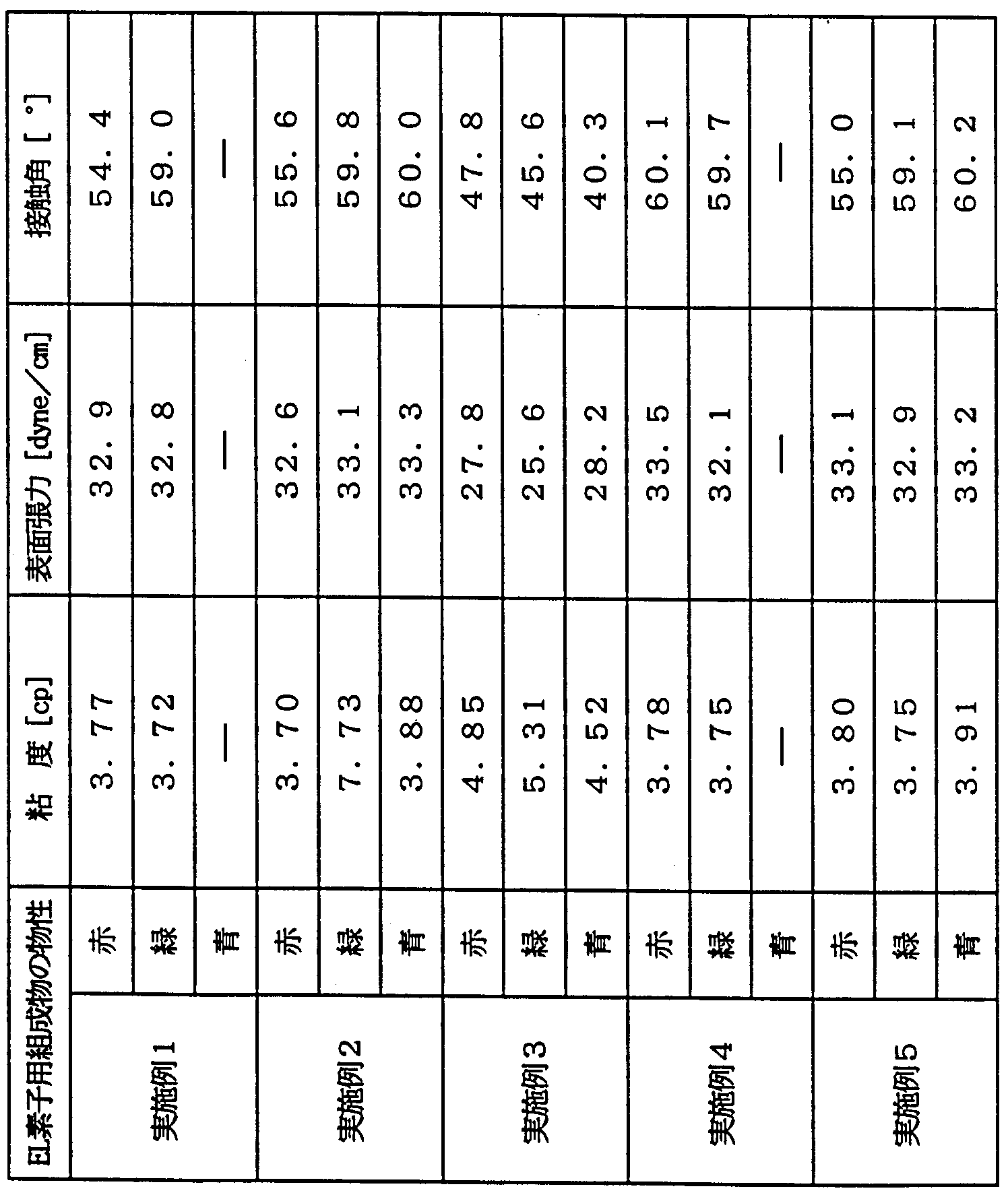
- red and green light-emitting materials shown in Tables 1 and 2 were patterned and applied using the ink jet printing apparatus 209 in the same manner as in Example 1, and then the film was heated at 150 ° C. in a nitrogen atmosphere. C, heat-treated for 4 hours to polymerize the precursor in the composition to form the respective light emitting layers 206 (red) and 207 (green).
- a hole injection / transport layer made of polyvinyl carbazole (PVK) was pattern-formed on the transparent pixel electrode 203 using the above-described ink jet printing apparatus 209. Virazolin dimer was applied thereon to form a blue light emitting layer 210.
- an A1—Li electrode 211 having a thickness of 0.8 ⁇ was formed as a cathode by a vapor deposition method to produce an organic EL device.
- each ITO transparent pixel electrode 800, 802, 803 and a partition 805 were formed on a glass substrate 804.
- an organic hole injecting and transporting material was mixed with the luminescent materials shown in Tables 1 and 2, and the respective luminescent layers 806 (red), 807 ( Green) and 808 (blue).
- a 1 to 1 electrode 8 13 having a thickness of 0.2111 as a cathode was formed by a vapor deposition method to produce an organic EL device.
- each ITO transparent pixel electrode 301, 302, 303 and a partition 304 were formed on a glass substrate 304.
- the red and green light-emitting materials shown in Tables 1 and 2 were patterned and applied using the ink-jet printing apparatus 310 in the same manner as in Example 1, and then were applied under a nitrogen atmosphere. Heat treatment was performed at 4 ° C. for 4 hours to polymerize the precursor in the composition, thereby forming each of the light emitting layers 303 (red) and 307 (green).
- a hole injection / transport layer 308 made of polyvinyl carbazole (PVK) was formed on the entire surface of the light emitting layers 306 and 307 and the transparent pixel electrode 303 by a coating method. Thereafter, a blue light emitting layer 309 made of a distyryl derivative was provided on the hole injecting and transporting layer 308 by a vacuum evaporation method.
- PVK polyvinyl carbazole
- the cathode 311 is naturally cut off and insulated by the partition walls 304 as described above, and is in a state of being patterned according to each of the pixel electrodes 301, 302, and 303.
- each ITO transparent pixel electrode 800, 802, 803 and a partition 805 were formed on a glass substrate 804 as shown in FIG.
- each of the light-emitting layers 806 (red), 807 (green), and 808 (blue) that emit red, green, and blue by heating for a period of time to polymerize the precursor in the composition ) was formed.
- a 0.1- jum electron transport layer 811 was formed by vacuum-depositing an undoped aluminum quinolinol complex.
- an A 1 —Li electrode 8 1 2 with a thickness of 0.8 ⁇ is formed as a cathode by vapor deposition.
- an organic EL device was manufactured.
- a predetermined voltage was applied to the device, and the voltage applied when observing the light emission luminance of lcd_m 2 was defined as a light emission start voltage [V, h ].
- the initial luminance after stabilization is 100%, a constant current is applied with a standard waveform to emit light continuously, and the change in luminance is measured until the luminance decreases to 50% of the initial luminance.
- the time is defined as the luminescence lifetime.
- the driving conditions were as follows: room temperature: 40 ° C, humidity: 23%, and current value: 2 O mA / cm 2 .
- the maximum absorption wavelength of each light emitting layer was measured.
- the evaluation was performed as follows.
- Examples 1 to 5 were all excellent in the light emitting characteristics of each light emitting layer and the film properties of the light emitting layer.
- the light emitting layer was made of a high molecular weight organic compound, no defect was observed in each light emitting layer, and a very good thin film was formed.
- the composition for an organic EL device and the method for producing an organic EL device of the present invention have been described in accordance with the illustrated examples. However, the present invention is not limited to these examples. Instead, for example, there may be a step of providing an arbitrary functional intermediate layer between the layers. Further, the fluorescent dye added to change the light emission characteristics is not limited to these.
- a layer made of, for example, 1,2,4-triazole derivative (TAZ) can be provided as a buffer layer between each layer, thereby further improving the light emission luminance and light emission lifetime. it can.
- TEZ 1,2,4-triazole derivative
- the method for manufacturing an organic EL device of the present invention includes a surface treatment such as a plasma treatment, a UV treatment, and a coupling treatment on the surface of the resin resist, the pixel electrode, and the lower layer so that the EL material is easily attached. May be performed. Further, the method for producing an organic EL device of the present invention can be applied to a method for producing an inorganic EL device.
- the organic EL display device of the present invention is applied to a low-information field such as a segment display and a simultaneous image display of the entire surface, for example, a picture, a character, a label, or the like, or has a dot, line, or surface shape. It can also be used as a light source.
- a rational design of the EL light emitting device is possible by selecting a wide range of light emitting materials.
- various display lights can be obtained by a combination of a light emitting material and a fluorescent dye.
- the size and pattern of the light-emitting element are arbitrarily and precisely set by forming and arranging the organic light-emitting layer, the hole injection transport layer and the electron injection transport layer of at least one color by an ink jet method. It becomes possible.
- the degree of freedom in setting conditions such as viscosity is large, and it is adjusted to conditions suitable for an ejection liquid for inkjet. It is easy to do.
- the conditions such as the film thickness and the number of dots can be arbitrarily adjusted, so that the light emitting characteristics of the light emitting layer can be easily controlled.
- the head can be freely moved on the transparent substrate, so that an element of an arbitrary size can be formed without limiting the substrate size.
- waste such as waste liquid can be eliminated as much as possible. This makes it possible to manufacture an inexpensive, large-screen, full-color display device.
- Luminescent material CN-PPV precursor PPV precursor Aluminum complex
- RGBRGBRGBRGB Example 1 2. 0 2. 2 3. 1 8000 8000 8000 210 230 200 600 500 400 Example 2 1. 7 1. 8 3.2 10000 10000 9000 230 230 180 600 500 410 Example 3 4. 0 3 5 3. 8 4000 5000 4000 150 180 100 580 510 420 Example 4 1.7 1.8 2. 2 10000 10000 10000 250 250 200 600 530 480 Example 5 3. 0 3.2 5.00 5000 5000 5000 200 200 200 590 530 420
- Example 1 o o o
- Example 2 o o o
- Example 4 o o o
- Example 5 o o o
Description
Claims
Priority Applications (8)
| Application Number | Priority Date | Filing Date | Title |
|---|---|---|---|
| KR10-2004-7011651A KR100493131B1 (ko) | 1996-11-25 | 1997-11-25 | 유기 el 소자 |
| US09/101,083 US6863961B2 (en) | 1996-11-25 | 1997-11-25 | Method of manufacturing organic EL element, organic EL element, and organic EL display device |
| KR10-2004-7011648A KR100498852B1 (ko) | 1996-11-25 | 1997-11-25 | 유기 el 소자의 제조 방법 |
| KR10-2004-7011649A KR100495744B1 (ko) | 1996-11-25 | 1997-11-25 | 유기 el 소자의 제조 방법 및 유기 el 소자 |
| EP97913435A EP0880303B1 (en) | 1996-11-25 | 1997-11-25 | Method of producing organic el elements, organic el elements and organic el display device |
| DE69727212T DE69727212T2 (de) | 1996-11-25 | 1997-11-25 | Verfahren zur herstellung organischer elektrolumineszenzelemente, organische elektrolumineszenzelemente und organische elektrolumineszenzanzeige-vorrichtung |
| US10/956,123 US7662425B2 (en) | 1996-11-25 | 2004-10-04 | Method of manufacturing organic EL element, organic EL element and organic EL display device |
| US12/651,267 US8614545B2 (en) | 1996-11-25 | 2009-12-31 | Organic EL display device having a bank formed to fill spaces between pixel electrodes |
Applications Claiming Priority (2)
| Application Number | Priority Date | Filing Date | Title |
|---|---|---|---|
| JP31382896A JP3899566B2 (ja) | 1996-11-25 | 1996-11-25 | 有機el表示装置の製造方法 |
| JP8/313828 | 1996-11-25 |
Related Child Applications (6)
| Application Number | Title | Priority Date | Filing Date |
|---|---|---|---|
| US09101083 A-371-Of-International | 1997-11-25 | ||
| US09/101,083 A-371-Of-International US6863961B2 (en) | 1996-11-25 | 1997-11-25 | Method of manufacturing organic EL element, organic EL element, and organic EL display device |
| US09/731,915 Division US6838192B2 (en) | 1996-11-25 | 2000-12-08 | Method of manufacturing organic EL element, organic EL element, and organic EL display device |
| US09/901,097 Division US20020136823A1 (en) | 1996-11-25 | 2001-07-10 | Method of manufacturing organic EL element, organic EL element, and organic EL display device |
| US09/983,414 Division US6833156B2 (en) | 1996-11-25 | 2001-10-24 | Method of manufacturing organic EL element, organic EL element, and organic EL display device |
| US10/166,704 Continuation US6821553B2 (en) | 1996-11-25 | 2002-06-12 | Method of manufacturing organic EL element, organic EL element, and organic EL display device |
Publications (1)
| Publication Number | Publication Date |
|---|---|
| WO1998024271A1 true WO1998024271A1 (fr) | 1998-06-04 |
Family
ID=18046006
Family Applications (1)
| Application Number | Title | Priority Date | Filing Date |
|---|---|---|---|
| PCT/JP1997/004283 WO1998024271A1 (fr) | 1996-11-25 | 1997-11-25 | Procede de production d'elements el organiques, elements el organiques et dispositif d'affichage el organique |
Country Status (8)
| Country | Link |
|---|---|
| US (7) | US6863961B2 (ja) |
| EP (4) | EP0880303B1 (ja) |
| JP (1) | JP3899566B2 (ja) |
| KR (4) | KR100498852B1 (ja) |
| CN (5) | CN1138458C (ja) |
| DE (2) | DE69736494T2 (ja) |
| TW (1) | TW553579U (ja) |
| WO (1) | WO1998024271A1 (ja) |
Cited By (58)
| Publication number | Priority date | Publication date | Assignee | Title |
|---|---|---|---|---|
| EP0961525A1 (en) * | 1997-08-29 | 1999-12-01 | Seiko Epson Corporation | Active matrix display |
| WO1999066483A1 (en) * | 1998-06-19 | 1999-12-23 | Cambridge Display Technology Ltd. | Backlit displays |
| EP0969701A1 (en) * | 1997-09-01 | 2000-01-05 | Seiko Epson Corporation | Electroluminescent device |
| GB2347015A (en) * | 1999-02-19 | 2000-08-23 | Cambridge Display Tech Ltd | Organic electroluminescent displays |
| US6580212B2 (en) | 1997-09-01 | 2003-06-17 | Cambridge Display Technology Ltd. | Display device with improved contrast |
| US6656519B2 (en) * | 1998-01-22 | 2003-12-02 | Nec Corporation | Multicolor organic electroluminescent panel and process for production thereof |
| US6712661B1 (en) * | 1998-09-17 | 2004-03-30 | Seiko Epson Corporation | Method for manufacturing electroluminescence device |
| JP2004524948A (ja) * | 2000-12-06 | 2004-08-19 | ウィルヘルム・テオドラス・ステファヌス・ハック | 圧縮二酸化炭素を使用するパターン化付着 |
| US6843937B1 (en) * | 1997-07-16 | 2005-01-18 | Seiko Epson Corporation | Composition for an organic EL element and method of manufacturing the organic EL element |
| US6872672B2 (en) | 1999-06-28 | 2005-03-29 | Semiconductor Energy Laboratory Co., Ltd. | Method of manufacturing an electro-optical device |
| EP1505648A3 (en) * | 1997-08-21 | 2005-08-10 | Seiko Epson Corporation | Active matrix display device |
| EP1505649A3 (en) * | 1997-07-02 | 2005-08-10 | Seiko Epson Corporation | Display device |
| US6982179B2 (en) | 2002-11-15 | 2006-01-03 | University Display Corporation | Structure and method of fabricating organic devices |
| US7063869B2 (en) * | 2001-06-15 | 2006-06-20 | Semiconductor Energy Laboratory Co., Ltd. | Printing device and method of manufacturing a light emitting device |
| US7131881B2 (en) * | 2001-08-30 | 2006-11-07 | Sharp Kabushiki Kaisha | Method of manufacturing organic EL device, and organic EL device |
| US7170086B2 (en) | 2002-09-19 | 2007-01-30 | Samsung Electronics Co., Ltd. | Organic electroluminescent device, electronic device and manufacturing method thereof |
| US7279194B2 (en) * | 2000-02-04 | 2007-10-09 | Semiconductor Energy Laboratory Co., Ltd. | Thin film formation apparatus and method of manufacturing self-light-emitting device using thin film formation apparatus |
| US7300686B2 (en) * | 2000-11-28 | 2007-11-27 | Seiko Epson Corporation | Organic electro-luminescent device, manufacturing method for the same, and electronic equipment |
| US7303274B2 (en) | 2000-03-31 | 2007-12-04 | Seiko Epson Corporation | Thin film formation method by ink jet method, ink jet apparatus, production method of organic EL device, and organic EL device |
| US7341760B2 (en) * | 2000-05-12 | 2008-03-11 | Semiconductor Energy Laboratory Co., Ltd. | Light-emitting device |
| US20080305245A1 (en) * | 1999-03-29 | 2008-12-11 | Cambridge Display Technology Limited | Composition, film manufacturing method, as well as functional device and manufacturing method therefor |
| US7510672B2 (en) | 2004-05-18 | 2009-03-31 | Merck Patent Gmbh | Formulation for ink-jet printing comprising semiconducting polymers |
| US7550173B2 (en) * | 2001-01-17 | 2009-06-23 | Semiconductor Energy Laboratory Co., Ltd. | Luminescent device and method of manufacturing same |
| US7662425B2 (en) * | 1996-11-25 | 2010-02-16 | Seiko Epson Corporation | Method of manufacturing organic EL element, organic EL element and organic EL display device |
| US7704650B2 (en) | 1999-10-29 | 2010-04-27 | 3M Innovative Properties Company | Donor sheet, color filter, organic EL element and method for producing them |
| US7771843B2 (en) | 2003-06-24 | 2010-08-10 | Samsung Mobile Display Co., Ltd. | Organic light-emitting device employing doped hole transporting layer and/or hole injecting layer |
| US7875308B2 (en) | 2002-06-28 | 2011-01-25 | Samsung Mobile Display Co., Ltd. | Organic electroluminescent device using a mixture of high and low molecular light-emitting substances as a light-emitting substance |
| US7887663B2 (en) | 2000-10-12 | 2011-02-15 | Sanyo Electric Co., Ltd. | Method for forming color filter, method for forming light emitting element layer, method for manufacturing color display device comprising them, or color display device |
| US7919341B2 (en) | 1999-10-13 | 2011-04-05 | Semiconductor Energy Laboratory Co., Ltd. | Thin film forming apparatus |
| CN101262725B (zh) * | 2007-03-08 | 2011-08-17 | 精工爱普生株式会社 | 发光装置及其制造方法和电子设备 |
| US20110278572A1 (en) * | 1999-10-26 | 2011-11-17 | Semiconductor Energy Laboratory Co., Ltd. | Electro-Optical Device |
| US8133748B2 (en) | 1999-10-12 | 2012-03-13 | Semiconductor Energy Laboratory Co., Ltd. | EL display device and method of manufacturing the same |
| CN103081150A (zh) * | 2010-09-02 | 2013-05-01 | 昭和电工株式会社 | El元件、el元件的制造方法、显示装置以及照明装置 |
| US9054344B2 (en) | 2010-01-20 | 2015-06-09 | Universal Display Corporation | Electroluminescent devices for lighting applications |
| WO2015192941A1 (de) | 2014-06-18 | 2015-12-23 | Merck Patent Gmbh | Zusammensetzungen für elektronische vorrichtungen |
| WO2015197156A1 (de) | 2014-06-25 | 2015-12-30 | Merck Patent Gmbh | Materialien für organische elektrolumineszenzvorrichtungen |
| WO2018104194A1 (de) | 2016-12-05 | 2018-06-14 | Merck Patent Gmbh | Materialien für organische elektrolumineszenzvorrichtungen |
| WO2018104193A1 (de) | 2016-12-05 | 2018-06-14 | Merck Patent Gmbh | Materialien für organische elektrolumineszenzvorrichtungen |
| WO2018127465A1 (de) | 2017-01-04 | 2018-07-12 | Merck Patent Gmbh | Materialien für organische elektrolumineszenzvorrichtungen |
| WO2018138306A1 (de) | 2017-01-30 | 2018-08-02 | Merck Patent Gmbh | Materialien für organische elektrolumineszenzvorrichtungen |
| WO2018149769A1 (de) | 2017-02-14 | 2018-08-23 | Merck Patent Gmbh | Materialien für organische elektrolumineszenzvorrichtungen |
| WO2019081391A1 (de) | 2017-10-24 | 2019-05-02 | Merck Patent Gmbh | Materialien für organische elektrolumineszenzvorrichtungen |
| WO2019145316A1 (de) | 2018-01-25 | 2019-08-01 | Merck Patent Gmbh | Materialien für organische elektrolumineszenzvorrichtungen |
| WO2019233904A1 (de) | 2018-06-07 | 2019-12-12 | Merck Patent Gmbh | Organische elektrolumineszenzvorrichtungen |
| WO2020011686A1 (de) | 2018-07-09 | 2020-01-16 | Merck Patent Gmbh | Materialien für organische elektrolumineszenzvorrichtungen |
| WO2020094542A1 (de) | 2018-11-06 | 2020-05-14 | Merck Patent Gmbh | 5,6-diphenyl-5,6-dihydro-dibenz[c,e][1,2]azaphosphorin- und 6-phenyl-6h-dibenzo[c,e][1,2]thiazin-5,5-dioxid-derivate und ähnliche verbindungen als organische elektrolumineszenzmaterialien für oleds |
| WO2020099307A1 (de) | 2018-11-15 | 2020-05-22 | Merck Patent Gmbh | Materialien für organische elektrolumineszenzvorrichtungen |
| WO2020127165A1 (de) | 2018-12-19 | 2020-06-25 | Merck Patent Gmbh | Materialien für organische elektrolumineszenzvorrichtungen |
| WO2021043755A1 (de) | 2019-09-03 | 2021-03-11 | Merck Patent Gmbh | Materialien für organische elektrolumineszenzvorrichtungen |
| WO2021151922A1 (de) | 2020-01-29 | 2021-08-05 | Merck Patent Gmbh | Benzimidazol-derivate |
| WO2022101171A1 (de) | 2020-11-10 | 2022-05-19 | Merck Patent Gmbh | Schwefelhaltige verbindungen für organische elektrolumineszenzvorrichtungen |
| WO2022117473A1 (de) | 2020-12-02 | 2022-06-09 | Merck Patent Gmbh | Heterocyclische verbindungen für organische elektrolumineszenzvorrichtungen |
| WO2022157343A1 (de) | 2021-01-25 | 2022-07-28 | Merck Patent Gmbh | Stickstoffhaltige verbindungen für organische elektrolumineszenzvorrichtungen |
| WO2022184601A1 (de) | 2021-03-02 | 2022-09-09 | Merck Patent Gmbh | Verbindungen für organische elektrolumineszenzvorrichtungen |
| WO2022194799A1 (de) | 2021-03-18 | 2022-09-22 | Merck Patent Gmbh | Heteroaromatische verbindungen für organische elektrolumineszenzvorrichtungen |
| WO2023213837A1 (de) | 2022-05-06 | 2023-11-09 | Merck Patent Gmbh | Cyclische verbindungen für organische elektrolumineszenzvorrichtungen |
| WO2024061948A1 (de) | 2022-09-22 | 2024-03-28 | Merck Patent Gmbh | Stickstoffenthaltende heterocyclen für organische elektrolumineszenzvorrichtungen |
| WO2024061942A1 (de) | 2022-09-22 | 2024-03-28 | Merck Patent Gmbh | Stickstoffenthaltende verbindungen für organische elektrolumineszenzvorrichtungen |
Families Citing this family (423)
| Publication number | Priority date | Publication date | Assignee | Title |
|---|---|---|---|---|
| EP1445793A3 (en) * | 1996-05-15 | 2004-09-01 | Seiko Epson Corporation | Thin film device provided with coating film, liquid crystal panel and electronic device, and method for making the thin film device |
| KR100509240B1 (ko) | 1997-02-17 | 2005-08-22 | 세이코 엡슨 가부시키가이샤 | 표시 장치 |
| US6462722B1 (en) | 1997-02-17 | 2002-10-08 | Seiko Epson Corporation | Current-driven light-emitting display apparatus and method of producing the same |
| JP3520396B2 (ja) | 1997-07-02 | 2004-04-19 | セイコーエプソン株式会社 | アクティブマトリクス基板と表示装置 |
| GB9715907D0 (en) | 1997-07-29 | 1997-10-01 | Cambridge Consultants | Electroluminescent device production process |
| WO1999012395A1 (fr) * | 1997-09-02 | 1999-03-11 | Seiko Epson Corporation | Procede de fabrication d'un element electroluminescent organique et element electroluminescent organique correspondant |
| CH692682A5 (de) * | 1997-10-06 | 2002-09-13 | Enz Electronic Ag | Anzeigeeinrichtung. |
| GB2376566B (en) * | 1997-10-14 | 2003-02-05 | Patterning Technologies Ltd | Method of forming an electronic device |
| CA2306384A1 (en) | 1997-10-14 | 1999-04-22 | Patterning Technologies Limited | Method of forming an electronic device |
| GB9803763D0 (en) * | 1998-02-23 | 1998-04-15 | Cambridge Display Tech Ltd | Display devices |
| KR100608543B1 (ko) | 1998-03-17 | 2006-08-03 | 세이코 엡슨 가부시키가이샤 | 표시장치의 제조방법 및 박막발광소자의 제조방법 |
| JP3646510B2 (ja) | 1998-03-18 | 2005-05-11 | セイコーエプソン株式会社 | 薄膜形成方法、表示装置およびカラーフィルタ |
| US7090890B1 (en) | 1998-04-13 | 2006-08-15 | The Trustees Of Princeton University | Modification of polymer optoelectronic properties after film formation by impurity addition or removal |
| CN1237496C (zh) * | 1998-07-24 | 2006-01-18 | 精工爱普生株式会社 | 显示装置 |
| JP3692844B2 (ja) * | 1998-07-24 | 2005-09-07 | セイコーエプソン株式会社 | 電界発光素子、及び電子機器 |
| JP4258860B2 (ja) * | 1998-09-04 | 2009-04-30 | セイコーエプソン株式会社 | 光伝達手段を備えた装置 |
| JP2000228284A (ja) * | 1998-12-01 | 2000-08-15 | Sanyo Electric Co Ltd | カラーel表示装置 |
| JP2000227770A (ja) | 1998-12-01 | 2000-08-15 | Sanyo Electric Co Ltd | カラーel表示装置 |
| JP2000227771A (ja) | 1998-12-01 | 2000-08-15 | Sanyo Electric Co Ltd | カラーel表示装置 |
| KR20010024923A (ko) | 1998-12-17 | 2001-03-26 | 야스카와 히데아키 | 발광 장치 |
| US6066357A (en) * | 1998-12-21 | 2000-05-23 | Eastman Kodak Company | Methods of making a full-color organic light-emitting display |
| JP3900724B2 (ja) * | 1999-01-11 | 2007-04-04 | セイコーエプソン株式会社 | 有機el素子の製造方法および有機el表示装置 |
| US6366025B1 (en) | 1999-02-26 | 2002-04-02 | Sanyo Electric Co., Ltd. | Electroluminescence display apparatus |
| US7821065B2 (en) * | 1999-03-02 | 2010-10-26 | Semiconductor Energy Laboratory Co., Ltd. | Semiconductor device comprising a thin film transistor comprising a semiconductor thin film and method of manufacturing the same |
| JP2000277260A (ja) | 1999-03-23 | 2000-10-06 | Seiko Epson Corp | 発光装置 |
| US6512504B1 (en) | 1999-04-27 | 2003-01-28 | Semiconductor Energy Laborayory Co., Ltd. | Electronic device and electronic apparatus |
| JP2000323276A (ja) * | 1999-05-14 | 2000-11-24 | Seiko Epson Corp | 有機el素子の製造方法、有機el素子およびインク組成物 |
| GB2351840A (en) | 1999-06-02 | 2001-01-10 | Seiko Epson Corp | Multicolour light emitting devices. |
| US8853696B1 (en) * | 1999-06-04 | 2014-10-07 | Semiconductor Energy Laboratory Co., Ltd. | Electro-optical device and electronic device |
| US7288420B1 (en) * | 1999-06-04 | 2007-10-30 | Semiconductor Energy Laboratory Co., Ltd. | Method for manufacturing an electro-optical device |
| TW527735B (en) * | 1999-06-04 | 2003-04-11 | Semiconductor Energy Lab | Electro-optical device |
| US6878297B1 (en) | 1999-06-09 | 2005-04-12 | Cambridge Display Technology, Limited | Method of producing organic light-emissive devices |
| DE60041532D1 (de) | 1999-06-10 | 2009-03-26 | Seiko Epson Corp | Licht emittierende vorrichtung |
| TW556357B (en) * | 1999-06-28 | 2003-10-01 | Semiconductor Energy Lab | Method of manufacturing an electro-optical device |
| TW504941B (en) | 1999-07-23 | 2002-10-01 | Semiconductor Energy Lab | Method of fabricating an EL display device, and apparatus for forming a thin film |
| EP1079262A3 (en) | 1999-08-05 | 2003-09-10 | Canon Kabushiki Kaisha | Method and apparatus for manufacturing a color filter |
| JP4226159B2 (ja) | 1999-08-06 | 2009-02-18 | シャープ株式会社 | 有機ledディスプレイの製造方法 |
| WO2001019142A1 (en) * | 1999-09-03 | 2001-03-15 | Uniax Corporation | Encapsulation of organic electronic devices |
| JP2001092413A (ja) * | 1999-09-24 | 2001-04-06 | Semiconductor Energy Lab Co Ltd | El表示装置および電子装置 |
| JP4854840B2 (ja) * | 1999-10-12 | 2012-01-18 | 株式会社半導体エネルギー研究所 | 発光装置の作製方法 |
| TW480722B (en) * | 1999-10-12 | 2002-03-21 | Semiconductor Energy Lab | Manufacturing method of electro-optical device |
| JP2001196162A (ja) | 1999-10-25 | 2001-07-19 | Seiko Epson Corp | 発光装置 |
| US7112115B1 (en) * | 1999-11-09 | 2006-09-26 | Semiconductor Energy Laboratory Co., Ltd. | Light emitting device and method of manufacturing the same |
| KR20010108148A (ko) * | 1999-11-29 | 2001-12-07 | 요트.게.아. 롤페즈 | 유기 전기발광 디바이스와 그 제조 방법 |
| JP2003515909A (ja) | 1999-11-29 | 2003-05-07 | コーニンクレッカ フィリップス エレクトロニクス エヌ ヴィ | 有機エレクトロルミネッセント装置とその製造方法 |
| JP4477726B2 (ja) * | 1999-12-09 | 2010-06-09 | シャープ株式会社 | 有機led素子の製造方法 |
| KR100387166B1 (ko) * | 1999-12-15 | 2003-06-12 | 닛뽄덴끼 가부시끼가이샤 | 유기 일렉트로 루미네선스 소자 |
| EP1122793A2 (en) * | 2000-02-01 | 2001-08-08 | Canon Kabushiki Kaisha | Production of organic luminescence device |
| TWI249363B (en) | 2000-02-25 | 2006-02-11 | Seiko Epson Corp | Organic electroluminescence device and manufacturing method therefor |
| TW495809B (en) | 2000-02-28 | 2002-07-21 | Semiconductor Energy Lab | Thin film forming device, thin film forming method, and self-light emitting device |
| JP2001244066A (ja) | 2000-03-01 | 2001-09-07 | Seiko Epson Corp | 発光装置 |
| TW495812B (en) | 2000-03-06 | 2002-07-21 | Semiconductor Energy Lab | Thin film forming device, method of forming a thin film, and self-light-emitting device |
| DE10012205A1 (de) * | 2000-03-13 | 2001-09-27 | Siemens Ag | Leuchtdiode auf der Basis von löslichen organischen Materialien |
| TWI226205B (en) | 2000-03-27 | 2005-01-01 | Semiconductor Energy Lab | Self-light emitting device and method of manufacturing the same |
| US6936485B2 (en) * | 2000-03-27 | 2005-08-30 | Semiconductor Energy Laboratory Co., Ltd. | Method of manufacturing a light emitting device |
| WO2001074121A1 (fr) | 2000-03-31 | 2001-10-04 | Seiko Epson Corporation | Dispositif electroluminescent organique et procede de fabrication |
| TW490997B (en) * | 2000-03-31 | 2002-06-11 | Seiko Epson Corp | Method of manufacturing organic EL element, and organic EL element |
| JP3882523B2 (ja) * | 2000-04-10 | 2007-02-21 | セイコーエプソン株式会社 | 有機エレクトロルミネッセンス装置 |
| JP4053209B2 (ja) * | 2000-05-01 | 2008-02-27 | 三星エスディアイ株式会社 | 有機elディスプレイの製造方法 |
| JP4683766B2 (ja) * | 2000-05-22 | 2011-05-18 | 株式会社半導体エネルギー研究所 | アクティブマトリクス型発光装置 |
| TW536836B (en) * | 2000-05-22 | 2003-06-11 | Semiconductor Energy Lab | Light emitting device and electrical appliance |
| TW538246B (en) * | 2000-06-05 | 2003-06-21 | Semiconductor Energy Lab | Display panel, display panel inspection method, and display panel manufacturing method |
| US7339317B2 (en) | 2000-06-05 | 2008-03-04 | Semiconductor Energy Laboratory Co., Ltd. | Light-emitting device having triplet and singlet compound in light-emitting layers |
| JP2001357974A (ja) * | 2000-06-13 | 2001-12-26 | Tdk Corp | 有機el素子の製造方法、および有機el素子 |
| JP2002008868A (ja) | 2000-06-16 | 2002-01-11 | Seiko Epson Corp | 面発光装置 |
| US6906458B2 (en) * | 2000-08-11 | 2005-06-14 | Seiko Epson Corporation | Method for manufacturing organic EL device, organic EL device and electronic apparatus |
| JP2002056989A (ja) | 2000-08-11 | 2002-02-22 | Seiko Epson Corp | 発光装置 |
| JP4675005B2 (ja) * | 2000-08-18 | 2011-04-20 | 株式会社半導体エネルギー研究所 | 発光装置、電子機器 |
| US6905784B2 (en) | 2000-08-22 | 2005-06-14 | Semiconductor Energy Laboratory Co., Ltd. | Light emitting device |
| US7430025B2 (en) * | 2000-08-23 | 2008-09-30 | Semiconductor Energy Laboratory Co., Ltd. | Portable electronic device |
| AU2001235796A1 (en) | 2000-08-30 | 2002-03-13 | Cambridge Display Technology Limited | A formulation for depositing a conjugated polymer layer |
| US7153592B2 (en) * | 2000-08-31 | 2006-12-26 | Fujitsu Limited | Organic EL element and method of manufacturing the same, organic EL display device using the element, organic EL material, and surface emission device and liquid crystal display device using the material |
| SG125891A1 (en) | 2000-09-08 | 2006-10-30 | Semiconductor Energy Lab | Light emitting device, method of manufacturing thesame, and thin film forming apparatus |
| US6617186B2 (en) | 2000-09-25 | 2003-09-09 | Dai Nippon Printing Co., Ltd. | Method for producing electroluminescent element |
| JP3972354B2 (ja) * | 2000-10-17 | 2007-09-05 | セイコーエプソン株式会社 | アクティブマトリクス基板及び液晶表示装置の製造方法 |
| US6980272B1 (en) * | 2000-11-21 | 2005-12-27 | Sarnoff Corporation | Electrode structure which supports self alignment of liquid deposition of materials |
| KR100358503B1 (ko) * | 2000-11-25 | 2002-10-30 | 주식회사 엘리아테크 | 유기 전계 발광 표시 패널 및 그 제조방법 |
| JP3628997B2 (ja) | 2000-11-27 | 2005-03-16 | セイコーエプソン株式会社 | 有機エレクトロルミネッセンス装置の製造方法 |
| CN1905126A (zh) * | 2000-11-27 | 2007-01-31 | 精工爱普生株式会社 | 有机电致发光装置及其电子装置 |
| JP3876684B2 (ja) * | 2000-12-21 | 2007-02-07 | セイコーエプソン株式会社 | カラーフィルタの製造方法、カラーフィルタの製造装置、液晶装置の製造方法、液晶装置の製造装置、el装置の製造方法、el装置の製造装置、材料の吐出方法、ヘッドの制御装置、電子機器 |
| JP2002190389A (ja) * | 2000-12-22 | 2002-07-05 | Nippon Steel Chem Co Ltd | 有機el素子の製造方法及び装置 |
| JP4139085B2 (ja) * | 2001-02-15 | 2008-08-27 | 三星エスディアイ株式会社 | 有機elデバイスおよびこの製造方法 |
| US8232116B2 (en) | 2001-02-28 | 2012-07-31 | Cambridge Display Technology Limited | Method for fabricating a polymer L.E.D. |
| CN100377380C (zh) * | 2001-02-28 | 2008-03-26 | 剑桥显示技术有限公司 | 供沉积在基材上的材料配方和方法 |
| JP4131114B2 (ja) | 2001-03-09 | 2008-08-13 | セイコーエプソン株式会社 | 発光装置、表示装置ならびに電子機器 |
| US6787063B2 (en) | 2001-03-12 | 2004-09-07 | Seiko Epson Corporation | Compositions, methods for producing films, functional elements, methods for producing functional elements, methods for producing electro-optical devices and methods for producing electronic apparatus |
| EP1386359A1 (en) | 2001-04-26 | 2004-02-04 | Koninklijke Philips Electronics N.V. | Electroluminescent device and method for manufacturing thereof |
| KR20030095955A (ko) * | 2001-04-26 | 2003-12-24 | 코닌클리케 필립스 일렉트로닉스 엔.브이. | 유기 전자발광 디바이스 및 그 제조 방법 |
| EP1388178A2 (en) * | 2001-05-14 | 2004-02-11 | CDT Oxford Limited | A method of providing a layer including a metal or silicon or germanium and oxygen on a surface |
| JP3969698B2 (ja) * | 2001-05-21 | 2007-09-05 | 株式会社半導体エネルギー研究所 | 発光装置の作製方法 |
| US7199515B2 (en) | 2001-06-01 | 2007-04-03 | Semiconductor Energy Laboratory Co., Ltd. | Organic light emitting element and light emitting device using the element |
| JP2002367787A (ja) * | 2001-06-05 | 2002-12-20 | Tohoku Pioneer Corp | 有機el表示装置及びその製造方法 |
| US20020197393A1 (en) * | 2001-06-08 | 2002-12-26 | Hideaki Kuwabara | Process of manufacturing luminescent device |
| JP2003017248A (ja) | 2001-06-27 | 2003-01-17 | Sony Corp | 電界発光素子 |
| CN100433406C (zh) * | 2001-07-04 | 2008-11-12 | 精工爱普生株式会社 | 电致发光基板的制造方法及制造装置与电子装置 |
| JP2003022892A (ja) | 2001-07-06 | 2003-01-24 | Semiconductor Energy Lab Co Ltd | 発光装置の製造方法 |
| JP5057619B2 (ja) | 2001-08-01 | 2012-10-24 | 株式会社半導体エネルギー研究所 | 半導体装置の作製方法 |
| GB2379083A (en) | 2001-08-20 | 2003-02-26 | Seiko Epson Corp | Inkjet printing on a substrate using two immiscible liquids |
| TWI306721B (en) | 2001-08-25 | 2009-02-21 | Cambridge Display Tech Ltd | Display device |
| US7333167B2 (en) | 2001-08-29 | 2008-02-19 | Seiko Epson Corporation | Electrooptical device and electronic equipment having resin film in light emitting region and sealing region |
| DK200101287A (da) | 2001-08-31 | 2003-03-01 | Bang & Olufsen As | Udlæsningsenhed og fremgangsmåde til dens fremstilling |
| JP2003086383A (ja) | 2001-09-10 | 2003-03-20 | Seiko Epson Corp | 発光装置 |
| GB2379415A (en) * | 2001-09-10 | 2003-03-12 | Seiko Epson Corp | Monitoring the deposition of organic polymer droplets onto a substrate |
| US20030166311A1 (en) * | 2001-09-12 | 2003-09-04 | Seiko Epson Corporation | Method for patterning, method for forming film, patterning apparatus, film formation apparatus, electro-optic apparatus and method for manufacturing the same, electronic equipment, and electronic apparatus and method for manufacturing the same |
| US6569706B2 (en) * | 2001-09-19 | 2003-05-27 | Osram Opto Semiconductors Gmbh | Fabrication of organic light emitting diode using selective printing of conducting polymer layers |
| US6680578B2 (en) | 2001-09-19 | 2004-01-20 | Osram Opto Semiconductors, Gmbh | Organic light emitting diode light source |
| US6590157B2 (en) * | 2001-09-21 | 2003-07-08 | Eastman Kodak Company | Sealing structure for highly moisture-sensitive electronic device element and method for fabrication |
| US8278828B1 (en) | 2001-10-23 | 2012-10-02 | Imaging Systems Technology | Large area organic LED display |
| US10211268B1 (en) | 2012-09-28 | 2019-02-19 | Imaging Systems Technology, Inc. | Large area OLED display |
| US8698706B1 (en) | 2001-10-23 | 2014-04-15 | Imaging Systems Technology, Inc. | Organic electroluminescent display device driving method and apparatus |
| US7808451B1 (en) * | 2001-10-23 | 2010-10-05 | Imaging Systems Technology, Inc. | Organic electroluminescent display device method and apparatus |
| US6861810B2 (en) * | 2001-10-23 | 2005-03-01 | Fpd Systems | Organic electroluminescent display device driving method and apparatus |
| JP4009817B2 (ja) | 2001-10-24 | 2007-11-21 | セイコーエプソン株式会社 | 発光装置および電子機器 |
| GB2381643A (en) | 2001-10-31 | 2003-05-07 | Cambridge Display Tech Ltd | Display drivers |
| GB2381644A (en) | 2001-10-31 | 2003-05-07 | Cambridge Display Tech Ltd | Display drivers |
| JP4269134B2 (ja) | 2001-11-06 | 2009-05-27 | セイコーエプソン株式会社 | 有機半導体装置 |
| TWI264121B (en) | 2001-11-30 | 2006-10-11 | Semiconductor Energy Lab | A display device, a method of manufacturing a semiconductor device, and a method of manufacturing a display device |
| US6953735B2 (en) | 2001-12-28 | 2005-10-11 | Semiconductor Energy Laboratory Co., Ltd. | Method for fabricating a semiconductor device by transferring a layer to a support with curvature |
| JP4066661B2 (ja) * | 2002-01-23 | 2008-03-26 | セイコーエプソン株式会社 | 有機el装置の製造装置および液滴吐出装置 |
| US6921148B2 (en) * | 2002-01-30 | 2005-07-26 | Seiko Epson Corporation | Liquid drop discharge head, discharge method and discharge device; electro optical device, method of manufacture thereof, and device for manufacture thereof; color filter, method of manufacture thereof, and device for manufacture thereof; and device incorporating backing, method of manufacture thereof, and device for manufacture thereof |
| US6878470B2 (en) | 2002-02-08 | 2005-04-12 | Fuji Photo Film Co., Ltd. | Visible image receiving material, conductive pattern material and organic electroluminescence element, using member having surface hydrophilicity |
| JP2003266738A (ja) * | 2002-03-19 | 2003-09-24 | Seiko Epson Corp | 吐出装置用ヘッドユニットおよびこれを備えた吐出装置、並びに液晶表示装置の製造方法、有機el装置の製造方法、電子放出装置の製造方法、pdp装置の製造方法、電気泳動表示装置の製造方法、カラーフィルタの製造方法、有機elの製造方法、スペーサ形成方法、金属配線形成方法、レンズ形成方法、レジスト形成方法および光拡散体形成方法 |
| WO2003079734A1 (en) * | 2002-03-20 | 2003-09-25 | Fuji Photo Film Co., Ltd. | Organic thin-film device and its production method |
| GB0207134D0 (en) | 2002-03-27 | 2002-05-08 | Cambridge Display Tech Ltd | Method of preparation of organic optoelectronic and electronic devices and devices thereby obtained |
| AU2003224378A1 (en) * | 2002-05-27 | 2003-12-12 | Koninklijke Philips Electronics N.V. | Method of providing a substrate surface with a patterned layer |
| US6858464B2 (en) | 2002-06-19 | 2005-02-22 | Semiconductor Energy Laboratory Co., Ltd. | Method of manufacturing light emitting device |
| TW200403956A (en) * | 2002-07-01 | 2004-03-01 | Seiko Epson Corp | Composition, film formation method and device, photoelectric device and its manufacturing method, organic EL device and its manufacturing method, device, manufacturing method and electronic machine |
| TWI276366B (en) | 2002-07-09 | 2007-03-11 | Semiconductor Energy Lab | Production apparatus and method of producing a light-emitting device by using the same apparatus |
| JP2004055159A (ja) * | 2002-07-16 | 2004-02-19 | Dainippon Screen Mfg Co Ltd | 有機el素子の製造方法および有機el表示装置 |
| JP4852224B2 (ja) * | 2002-07-30 | 2012-01-11 | セイコーエプソン株式会社 | 有機el装置の製造装置 |
| JP4165692B2 (ja) * | 2002-08-05 | 2008-10-15 | 大日本印刷株式会社 | エレクトロルミネッセント素子の製造方法 |
| GB0218202D0 (en) | 2002-08-06 | 2002-09-11 | Avecia Ltd | Organic light emitting diodes |
| JP3729262B2 (ja) | 2002-08-29 | 2005-12-21 | セイコーエプソン株式会社 | エレクトロルミネセンス装置及び電子機器 |
| US7531377B2 (en) | 2002-09-03 | 2009-05-12 | Cambridge Display Technology Limited | Optical device |
| US7098060B2 (en) | 2002-09-06 | 2006-08-29 | E.I. Du Pont De Nemours And Company | Methods for producing full-color organic electroluminescent devices |
| JP4440523B2 (ja) * | 2002-09-19 | 2010-03-24 | 大日本印刷株式会社 | インクジェット法による有機el表示装置及びカラーフィルターの製造方法、製造装置 |
| JP4701580B2 (ja) * | 2002-09-30 | 2011-06-15 | セイコーエプソン株式会社 | 電気光学装置およびその製造方法、電子機器 |
| GB0224121D0 (en) * | 2002-10-16 | 2002-11-27 | Microemissive Displays Ltd | Method of patterning a functional material on to a substrate |
| JP3997888B2 (ja) | 2002-10-25 | 2007-10-24 | セイコーエプソン株式会社 | 電気光学装置、電気光学装置の製造方法及び電子機器 |
| EP1416028A1 (en) | 2002-10-30 | 2004-05-06 | Covion Organic Semiconductors GmbH | New method for the production of monomers useful in the manufacture of semiconductive polymers |
| CN100544533C (zh) * | 2002-11-11 | 2009-09-23 | 株式会社半导体能源研究所 | 发光装置的制造方法 |
| US6891326B2 (en) | 2002-11-15 | 2005-05-10 | Universal Display Corporation | Structure and method of fabricating organic devices |
| US20040096570A1 (en) * | 2002-11-15 | 2004-05-20 | Michael Weaver | Structure and method of fabricating organic devices |
| JP4719468B2 (ja) * | 2002-11-27 | 2011-07-06 | 株式会社アルバック | 小滴アライメントの影響並びに小滴体積許容差及び誤差を軽減するマスキングを含む工業マイクロデポジションシステム |
| GB0227778D0 (en) | 2002-11-28 | 2003-01-08 | Cambridge Display Tech Ltd | Droplet-deposition related methods and apparatus |
| US20040108061A1 (en) * | 2002-12-06 | 2004-06-10 | Eastman Kodak Company | Apparatus and method for making a light-emitting display |
| JPWO2004058850A1 (ja) * | 2002-12-25 | 2006-04-27 | 株式会社半導体エネルギー研究所 | 高分子化合物、電界発光素子及び発光装置 |
| US7112113B2 (en) * | 2002-12-25 | 2006-09-26 | Semiconductor Energy Laboratory Co., Ltd. | Manufacturing method of display device |
| JP4830254B2 (ja) * | 2003-01-23 | 2011-12-07 | セイコーエプソン株式会社 | 有機el装置の製造方法及び電子機器 |
| CN100401342C (zh) * | 2003-01-27 | 2008-07-09 | 东芝松下显示技术有限公司 | 制造有机el显示器的方法 |
| JP4595946B2 (ja) * | 2003-01-28 | 2010-12-08 | セイコーエプソン株式会社 | 発光体とその製造方法及び電気光学装置並びに電子機器 |
| JP3966283B2 (ja) | 2003-01-28 | 2007-08-29 | セイコーエプソン株式会社 | 発光体とその製造方法及び製造装置、電気光学装置並びに電子機器 |
| US7275812B2 (en) * | 2003-01-29 | 2007-10-02 | Fujifilm Corporation | Ink jet head and recording apparatus using the same |
| US20040151829A1 (en) * | 2003-01-31 | 2004-08-05 | Eastman Kodak Company | Optimizing OLED emission |
| JP4311050B2 (ja) * | 2003-03-18 | 2009-08-12 | セイコーエプソン株式会社 | 機能液滴吐出ヘッドの駆動制御方法および機能液滴吐出装置 |
| CN1764551A (zh) | 2003-03-27 | 2006-04-26 | 纳幕尔杜邦公司 | 转移热敏材料到衬底的方法和施主元件 |
| JP2004304009A (ja) * | 2003-03-31 | 2004-10-28 | Canon Inc | 有機薄膜トランジスタ |
| JP2004298787A (ja) * | 2003-03-31 | 2004-10-28 | Seiko Epson Corp | 描画装置、電子光学装置及び電子機器 |
| US7018007B2 (en) * | 2003-04-16 | 2006-03-28 | Osram Opto Semiconductors Gmbh | Ink-jet pocket printing |
| JP4120455B2 (ja) * | 2003-04-22 | 2008-07-16 | セイコーエプソン株式会社 | パターンの形成方法及びデバイスの製造方法 |
| JP3823981B2 (ja) * | 2003-05-12 | 2006-09-20 | セイコーエプソン株式会社 | パターンと配線パターン形成方法、デバイスとその製造方法、電気光学装置、電子機器及びアクティブマトリクス基板の製造方法 |
| ATE401672T1 (de) | 2003-05-12 | 2008-08-15 | Cambridge Entpr Ltd | Herstellung einer polymeren vorrichtung |
| JP4103830B2 (ja) * | 2003-05-16 | 2008-06-18 | セイコーエプソン株式会社 | パターンの形成方法及びパターン形成装置、デバイスの製造方法、アクティブマトリクス基板の製造方法 |
| GB0311234D0 (en) | 2003-05-16 | 2003-06-18 | Isis Innovation | Organic phosphorescent material and organic optoelectronic device |
| US6998492B2 (en) * | 2003-05-16 | 2006-02-14 | Semiconductor Energy Laboratory Co., Ltd. | Organometallic complex and light-emitting element containing the same |
| DE112004000838T5 (de) * | 2003-05-21 | 2006-03-30 | Dow Global Technologies, Inc., Midland | Mischung von Viskositätsmodifzierungsmittel und lumineszenter Verbindung |
| JP4651918B2 (ja) * | 2003-05-21 | 2011-03-16 | 東北パイオニア株式会社 | 有機elパネルの製造方法 |
| CN1768093B (zh) | 2003-05-30 | 2010-06-09 | 默克专利有限公司 | 聚合物 |
| JP2005019955A (ja) * | 2003-05-30 | 2005-01-20 | Seiko Epson Corp | 薄膜パターンの形成方法及びデバイスの製造方法、電気光学装置及び電子機器 |
| US7690781B2 (en) | 2003-06-04 | 2010-04-06 | Mimaki Engineering Co., Ltd. | Ink jet printer using UV ink |
| TWI237413B (en) * | 2003-06-06 | 2005-08-01 | Chi Mei Optoelectronics Corp | Organic electro-luminescent device array and fabrication method thereof |
| EP1491568A1 (en) | 2003-06-23 | 2004-12-29 | Covion Organic Semiconductors GmbH | Semiconductive Polymers |
| US7153539B2 (en) * | 2003-06-24 | 2006-12-26 | Eastman Kodak Company | Apparatus and method of color tuning a light-emitting display |
| US20040265481A1 (en) * | 2003-06-27 | 2004-12-30 | Yoshihiro Kobayashi | Method for manufacturing electroluminescent element |
| JP3757960B2 (ja) * | 2003-07-11 | 2006-03-22 | セイコーエプソン株式会社 | 液滴吐出装置、電気光学装置の製造方法、電子機器の製造方法 |
| US7438944B2 (en) | 2003-07-11 | 2008-10-21 | Seiko Epson Corporation | Droplet information measuring method and apparatus therefor, film pattern forming method, device manufacturing method, droplet discharge apparatus, electro-optical apparatus, and electronic apparatus |
| WO2005007418A2 (en) * | 2003-07-18 | 2005-01-27 | Koninklijke Philips Electronics N.V. | Thin film patterning arrangement |
| US7275972B2 (en) | 2003-08-22 | 2007-10-02 | 3M Innovative Properties Company | Method of making an electroluminescent device having a patterned emitter layer and non-patterned emitter layer |
| US20050048314A1 (en) * | 2003-08-28 | 2005-03-03 | Homer Antoniadis | Light emitting polymer devices with improved efficiency and lifetime |
| DE10340711A1 (de) | 2003-09-04 | 2005-04-07 | Covion Organic Semiconductors Gmbh | Elektronische Vorrichtung enthaltend organische Halbleiter |
| JP2005085604A (ja) * | 2003-09-09 | 2005-03-31 | Seiko Epson Corp | 有機金属化合物の薄膜形成方法、有機金属化合物薄膜、およびこれを備えた有機電子デバイスの製造方法、有機電子デバイス、有機エレクトロルミネッセンスの製造方法、有機エレクトロルミネッセンス、及び電子機器 |
| KR100543003B1 (ko) | 2003-09-15 | 2006-01-20 | 삼성에스디아이 주식회사 | 풀칼라 유기 전계 발광 소자 및 그의 제조 방법 |
| TW200521599A (en) * | 2003-10-14 | 2005-07-01 | Seiko Epson Corp | Electro-optical device, its manufacturing method and electronic instrument |
| JP2005123083A (ja) * | 2003-10-17 | 2005-05-12 | Dainippon Screen Mfg Co Ltd | 塗布組成物および有機el素子の製造方法 |
| US20070248839A1 (en) | 2003-11-10 | 2007-10-25 | Towns Carl R | Dibenzosilol Polymers, Their Preparation and Uses |
| US20050100657A1 (en) * | 2003-11-10 | 2005-05-12 | Macpherson Charles D. | Organic material with a region including a guest material and organic electronic devices incorporating the same |
| JP3915806B2 (ja) * | 2003-11-11 | 2007-05-16 | セイコーエプソン株式会社 | 電気光学装置および電子機器 |
| KR20050050487A (ko) * | 2003-11-25 | 2005-05-31 | 삼성에스디아이 주식회사 | 풀칼라 유기 전계 발광 소자 |
| KR100659530B1 (ko) * | 2003-11-26 | 2006-12-19 | 삼성에스디아이 주식회사 | 풀칼라 유기전계발광소자 |
| KR101137797B1 (ko) | 2003-12-15 | 2012-04-20 | 가부시키가이샤 한도오따이 에네루기 켄큐쇼 | 박막 집적회로장치의 제조방법, 비접촉형 박막집적회로장치 및 그 제조 방법, 비접촉형 박막 집적회로장치를 가지는 아이디 태그 및 동전 |
| GB0329364D0 (en) | 2003-12-19 | 2004-01-21 | Cambridge Display Tech Ltd | Optical device |
| KR100970253B1 (ko) * | 2003-12-19 | 2010-07-16 | 삼성전자주식회사 | 발광소자의 제조 방법 |
| US7271076B2 (en) * | 2003-12-19 | 2007-09-18 | Semiconductor Energy Laboratory Co., Ltd. | Manufacturing method of thin film integrated circuit device and manufacturing method of non-contact type thin film integrated circuit device |
| US7566010B2 (en) | 2003-12-26 | 2009-07-28 | Semiconductor Energy Laboratory Co., Ltd. | Securities, chip mounting product, and manufacturing method thereof |
| KR100663028B1 (ko) * | 2003-12-30 | 2006-12-28 | 엘지.필립스 엘시디 주식회사 | 유기 전계 발광 소자 및 그의 제조 방법 |
| GB0401613D0 (en) | 2004-01-26 | 2004-02-25 | Cambridge Display Tech Ltd | Organic light emitting diode |
| CN100502018C (zh) * | 2004-02-06 | 2009-06-17 | 株式会社半导体能源研究所 | 薄膜集成电路的制造方法和元件基片 |
| JP2005268202A (ja) * | 2004-02-16 | 2005-09-29 | Seiko Epson Corp | 有機エレクトロルミネッセンス装置、有機エレクトロルミネッセンス装置の製造方法、及び電子機器 |
| KR100712096B1 (ko) * | 2004-02-19 | 2007-04-27 | 삼성에스디아이 주식회사 | 유기전계 발광표시장치의 제조방법 |
| JP3994998B2 (ja) * | 2004-03-03 | 2007-10-24 | セイコーエプソン株式会社 | 発光装置、発光装置の製造方法及び電子機器 |
| JP4281584B2 (ja) * | 2004-03-04 | 2009-06-17 | セイコーエプソン株式会社 | 半導体装置の製造方法 |
| US7067841B2 (en) * | 2004-04-22 | 2006-06-27 | E. I. Du Pont De Nemours And Company | Organic electronic devices |
| JP2005317439A (ja) | 2004-04-30 | 2005-11-10 | Seiko Epson Corp | 表示パネル及び表示装置 |
| TWI262538B (en) * | 2004-04-30 | 2006-09-21 | Sharp Kk | Component placement substrate and production method thereof |
| DE102004023420A1 (de) * | 2004-05-12 | 2005-12-08 | Lisa Dräxlmaier GmbH | Verfahren zum Herstellen einer kombinierten Piezo-/Leuchtfolie und Betätigungselement mit einer derartigen Piezo-/Leuchtfolie |
| KR101215860B1 (ko) | 2004-05-21 | 2012-12-31 | 가부시키가이샤 한도오따이 에네루기 켄큐쇼 | 발광 소자 및 그 소자를 사용하는 발광 장치 |
| US20050264179A1 (en) * | 2004-05-27 | 2005-12-01 | Sigma Laboratories Of Arizona, Inc. | Large-area electroluminescent light-emitting devices |
| JP2006013139A (ja) * | 2004-06-25 | 2006-01-12 | Seiko Epson Corp | 有機el装置とその製造方法並びに電子機器 |
| US20060001021A1 (en) * | 2004-06-30 | 2006-01-05 | Motorola, Inc. | Multiple semiconductor inks apparatus and method |
| US20060022174A1 (en) * | 2004-07-27 | 2006-02-02 | General Electric Company | Electroactive chemical composition and method of coating |
| GB2416621A (en) | 2004-07-27 | 2006-02-01 | Cambridge Display Tech Ltd | Laminated interconnects for opto-electronic device modules |
| JP4103865B2 (ja) * | 2004-07-27 | 2008-06-18 | セイコーエプソン株式会社 | 有機el表示装置の製造方法 |
| WO2006013373A2 (en) | 2004-08-04 | 2006-02-09 | Cambridge Display Technology Limited | Organic electroluminescent device |
| TWI233319B (en) * | 2004-08-10 | 2005-05-21 | Ind Tech Res Inst | Full-color organic electroluminescence device and display panel using the same |
| KR20060019099A (ko) * | 2004-08-26 | 2006-03-03 | 삼성전자주식회사 | 유기 발광 표시 장치 및 이의 제조 방법 |
| JP4158755B2 (ja) * | 2004-09-30 | 2008-10-01 | セイコーエプソン株式会社 | 機能膜の製造方法、薄膜トランジスタの製造方法 |
| KR100770578B1 (ko) * | 2004-11-30 | 2007-10-26 | 주식회사 대우일렉트로닉스 | 유기 전계발광 소자 |
| GB0427266D0 (en) | 2004-12-13 | 2005-01-12 | Cambridge Display Tech Ltd | Phosphorescent OLED |
| US20060132028A1 (en) * | 2004-12-16 | 2006-06-22 | Lexmark International, Inc. | Electroluminescent display construction using printing technology |
| KR20070054186A (ko) * | 2004-12-17 | 2007-05-28 | 샤프 가부시키가이샤 | 유기 일렉트로루미네센스 디스플레이의 제조방법 및제조장치 |
| GB0428444D0 (en) | 2004-12-29 | 2005-02-02 | Cambridge Display Tech Ltd | Conductive polymer compositions in opto-electrical devices |
| GB0428445D0 (en) | 2004-12-29 | 2005-02-02 | Cambridge Display Tech Ltd | Blue-shifted triarylamine polymer |
| US7268006B2 (en) | 2004-12-30 | 2007-09-11 | E.I. Du Pont De Nemours And Company | Electronic device including a guest material within a layer and a process for forming the same |
| US20060145598A1 (en) * | 2004-12-30 | 2006-07-06 | Macpherson Charles D | Electronic devices and process for forming the same |
| JP5258302B2 (ja) | 2004-12-30 | 2013-08-07 | イー・アイ・デュポン・ドウ・ヌムール・アンド・カンパニー | 有機電子デバイスおよび方法 |
| JP2006196298A (ja) * | 2005-01-13 | 2006-07-27 | Toshiba Matsushita Display Technology Co Ltd | 有機el表示装置の製造方法 |
| JP4548121B2 (ja) | 2005-01-14 | 2010-09-22 | セイコーエプソン株式会社 | 発光素子の製造方法 |
| KR101108148B1 (ko) * | 2005-02-03 | 2012-02-09 | 삼성모바일디스플레이주식회사 | 유기 전계 발광 소자 및 이의 제조 방법 |
| JP4311360B2 (ja) | 2005-02-25 | 2009-08-12 | セイコーエプソン株式会社 | 発光素子、発光装置および電子機器 |
| TWI361018B (en) | 2005-04-18 | 2012-03-21 | Sony Corp | Display device and a method of manufacturing the s |
| JP4793071B2 (ja) * | 2005-04-18 | 2011-10-12 | ソニー株式会社 | 表示装置および表示装置の製造方法 |
| US7510951B2 (en) | 2005-05-12 | 2009-03-31 | Lg Chem, Ltd. | Method for forming high-resolution pattern with direct writing means |
| KR100833017B1 (ko) * | 2005-05-12 | 2008-05-27 | 주식회사 엘지화학 | 직접 패턴법을 이용한 고해상도 패턴형성방법 |
| DE102005022903A1 (de) | 2005-05-18 | 2006-11-23 | Merck Patent Gmbh | Lösungen organischer Halbleiter |
| GB0510382D0 (en) | 2005-05-20 | 2005-06-29 | Cambridge Display Tech Ltd | Ink jet printing compositions in opto-electrical devices |
| JP4736544B2 (ja) * | 2005-06-01 | 2011-07-27 | セイコーエプソン株式会社 | 電気光学装置及び電子機器 |
| JP4613700B2 (ja) * | 2005-06-01 | 2011-01-19 | セイコーエプソン株式会社 | 電気光学装置及び電子機器 |
| GB0514476D0 (en) * | 2005-07-14 | 2005-08-17 | Cambridge Display Tech Ltd | Conductive polymer compositions in opto-electrical devices |
| US20070096640A1 (en) * | 2005-08-19 | 2007-05-03 | Gang Yu | Methods for producing full color organic electroluminescent devices |
| GB0517195D0 (en) | 2005-08-23 | 2005-09-28 | Cambridge Display Tech Ltd | Molecular electronic device structures and fabrication methods |
| DE112006002220B4 (de) | 2005-08-23 | 2018-05-24 | Cambridge Display Technology Ltd. | Organische elektronische Vorrichtungsstrukturen und Herstellungsverfahren |
| JP2007103349A (ja) * | 2005-09-08 | 2007-04-19 | Seiko Epson Corp | 膜パターンの形成方法、有機el装置の製造方法、カラーフィルタ基板の製造方法、液晶表示装置の製造方法 |
| GB0518968D0 (en) | 2005-09-16 | 2005-10-26 | Cdt Oxford Ltd | Organic light-emitting device |
| JP4483757B2 (ja) | 2005-09-30 | 2010-06-16 | セイコーエプソン株式会社 | 有機el装置及び光学装置 |
| US20070090758A1 (en) * | 2005-10-21 | 2007-04-26 | Kwasny David M | Electroluminescent panel |
| JP2007122914A (ja) | 2005-10-25 | 2007-05-17 | Sharp Corp | 有機エレクトロルミネッセンスディスプレイの製造方法及びそれに用いる製造装置 |
| US7990047B2 (en) * | 2005-10-28 | 2011-08-02 | Samsung Electronics Co., Ltd. | Organic light emitting diode display and method of manufacturing the same |
| KR101143006B1 (ko) | 2005-10-28 | 2012-05-08 | 삼성전자주식회사 | 유기 발광 표시 장치 및 그 제조 방법 |
| JP2008010805A (ja) * | 2005-11-11 | 2008-01-17 | Sumitomo Chemical Co Ltd | 有機エレクトロルミネッセンス素子 |
| KR100661642B1 (ko) * | 2005-11-28 | 2006-12-26 | 삼성전자주식회사 | 표시장치의 제조방법과 이에 의한 표시장치 |
| JP2007188862A (ja) | 2005-12-13 | 2007-07-26 | Canon Inc | 有機el発光装置およびその製造方法 |
| GB0526185D0 (en) | 2005-12-22 | 2006-02-01 | Cambridge Display Tech Ltd | Electronic device |
| GB2433509A (en) | 2005-12-22 | 2007-06-27 | Cambridge Display Tech Ltd | Arylamine polymer |
| GB0526393D0 (en) | 2005-12-23 | 2006-02-08 | Cdt Oxford Ltd | Light emissive device |
| KR100900550B1 (ko) | 2006-01-16 | 2009-06-02 | 삼성전자주식회사 | 표시장치와 그 제조방법 |
| GB2434915A (en) | 2006-02-03 | 2007-08-08 | Cdt Oxford Ltd | Phosphoescent OLED for full colour display |
| CN100462846C (zh) * | 2006-02-15 | 2009-02-18 | 虹创科技股份有限公司 | 薄膜图案层的制造方法 |
| US9214636B2 (en) * | 2006-02-28 | 2015-12-15 | Idemitsu Kosan Co., Ltd. | Organic electroluminescence device |
| US20070215883A1 (en) * | 2006-03-20 | 2007-09-20 | Dixon Michael J | Electroluminescent Devices, Subassemblies for use in Making Electroluminescent Devices, and Dielectric Materials, Conductive Inks and Substrates Related Thereto |
| CN101411002B (zh) | 2006-04-05 | 2010-10-13 | 夏普株式会社 | 有机电致发光显示装置的制造方法 |
| TW200739982A (en) * | 2006-04-06 | 2007-10-16 | Nat Univ Chung Cheng | Method for manufacturing full-color organic light-emitting diode array based on microcontact printing technology |
| WO2007117668A2 (en) * | 2006-04-07 | 2007-10-18 | Qd Vision, Inc. | Methods and articles including nanomaterial |
| GB2437113B (en) | 2006-04-12 | 2008-11-26 | Cambridge Display Tech Ltd | Light-emissive display and method of manufacturing the same |
| WO2007120877A2 (en) * | 2006-04-14 | 2007-10-25 | Qd Vision, Inc. | Transfer surface for manufacturing a light emitting device |
| JP4795268B2 (ja) * | 2006-04-20 | 2011-10-19 | キヤノン株式会社 | 有機発光素子 |
| JP4904903B2 (ja) * | 2006-04-20 | 2012-03-28 | 大日本印刷株式会社 | 有機エレクトロルミネッセンス素子の製造方法 |
| GB2440934B (en) | 2006-04-28 | 2009-12-16 | Cdt Oxford Ltd | Opto-electrical polymers and devices |
| JP5061184B2 (ja) * | 2006-06-05 | 2012-10-31 | イー・アイ・デュポン・ドウ・ヌムール・アンド・カンパニー | 有機発光ダイオードの形成方法、およびその方法によって製造されたデバイス |
| WO2008108798A2 (en) | 2006-06-24 | 2008-09-12 | Qd Vision, Inc. | Methods for depositing nanomaterial, methods for fabricating a device, and methods for fabricating an array of devices |
| WO2008105792A2 (en) * | 2006-06-24 | 2008-09-04 | Qd Vision, Inc. | Methods for depositing nanomaterial, methods for fabricating a device, methods for fabricating an array of devices and compositions |
| WO2008111947A1 (en) * | 2006-06-24 | 2008-09-18 | Qd Vision, Inc. | Methods and articles including nanomaterial |
| US20090263567A1 (en) | 2006-08-01 | 2009-10-22 | Cambridge Display Technology Limited | Methods of Manufacturing Opto-Electrical Devices |
| GB2441355B (en) | 2006-08-31 | 2009-05-20 | Cambridge Display Tech Ltd | Organic electronic device |
| GB2441354B (en) | 2006-08-31 | 2009-07-29 | Cambridge Display Tech Ltd | Display drive systems |
| GB0617167D0 (en) | 2006-08-31 | 2006-10-11 | Cdt Oxford Ltd | Compounds for use in opto-electrical devices |
| GB0618698D0 (en) | 2006-09-22 | 2006-11-01 | Cambridge Display Tech Ltd | Molecular electronic device fabrication methods and structures |
| TWI378740B (en) * | 2006-10-04 | 2012-12-01 | Ritdisplay Corp | Full-color organic light emitting diode display panel and method thereof |
| JP4605134B2 (ja) * | 2006-10-05 | 2011-01-05 | セイコーエプソン株式会社 | 液状体配置方法、カラーフィルタの製造方法、有機el表示装置の製造方法 |
| GB0620045D0 (en) | 2006-10-10 | 2006-11-22 | Cdt Oxford Ltd | Otpo-electrical devices and methods of making the same |
| DE102007029915B4 (de) * | 2006-12-20 | 2017-03-30 | Lg Display Co., Ltd. | Organisches Elektrolumineszenzbauteil und Verfahren zum Herstellen desselben |
| US20100035377A1 (en) * | 2006-12-22 | 2010-02-11 | Cbrite Inc. | Transfer Coating Method |
| TW200842401A (en) * | 2006-12-22 | 2008-11-01 | Cbrite Inc | Hemispherical coating method for micro-elements |
| US20080166566A1 (en) * | 2006-12-29 | 2008-07-10 | Shiva Prakash | Process for forming an organic light-emitting diode and devices made by the process |
| US20080218068A1 (en) | 2007-03-05 | 2008-09-11 | Cok Ronald S | Patterned inorganic led device |
| GB2448175B (en) | 2007-04-04 | 2009-07-22 | Cambridge Display Tech Ltd | Thin film transistor |
| TWI343648B (en) | 2007-04-19 | 2011-06-11 | Au Optronics Corp | Organic electroluminescent structure and method of making the same |
| JP2008271317A (ja) * | 2007-04-23 | 2008-11-06 | Sumitomo Chemical Co Ltd | 照明光通信システムおよび照明光通信用の送信装置 |
| KR100872396B1 (ko) * | 2007-05-03 | 2008-12-08 | 한국기계연구원 | 발광 광고지 및 그 제조방법 |
| CN101055922B (zh) * | 2007-05-09 | 2012-04-25 | 友达光电股份有限公司 | 有机电致发光结构及其制作方法 |
| KR100858824B1 (ko) * | 2007-05-31 | 2008-09-17 | 삼성에스디아이 주식회사 | 유기 발광 소자 및 이의 제조 방법 |
| JP2008311059A (ja) * | 2007-06-14 | 2008-12-25 | Rohm Co Ltd | 有機エレクトロルミネセンス素子及びその製造方法 |
| KR101672553B1 (ko) * | 2007-06-25 | 2016-11-03 | 큐디 비젼, 인크. | 조성물 및 나노물질의 침착을 포함하는 방법 |
| TW200907469A (en) * | 2007-08-14 | 2009-02-16 | Ind Tech Res Inst | Display panel and fabricating method thereof |
| GB2454867B (en) | 2007-11-09 | 2010-02-03 | Cambridge Display Tech Ltd | Electroluminescent devices comprising bus bar |
| US20090130296A1 (en) * | 2007-11-15 | 2009-05-21 | Universal Display Corporation | Fabrication of Organic Electronic Devices by Ink-Jet Printing at Low Temperatures |
| GB2454890B (en) | 2007-11-21 | 2010-08-25 | Limited Cambridge Display Technology | Light-emitting device and materials therefor |
| WO2009079327A1 (en) | 2007-12-14 | 2009-06-25 | E. I. Du Pont De Nemours And Company | Backplane structures for electronic devices |
| GB2455726A (en) * | 2007-12-18 | 2009-06-24 | Motorola Inc | Printable organic composition for organic electronics |
| GB2455747B (en) | 2007-12-19 | 2011-02-09 | Cambridge Display Tech Ltd | Electronic devices and methods of making the same using solution processing techniques |
| US7888169B2 (en) * | 2007-12-26 | 2011-02-15 | Organicid, Inc. | Organic semiconductor device and method of manufacturing the same |
| US8154700B2 (en) * | 2007-12-28 | 2012-04-10 | E.I. Du Pont De Nemours And Company | Electronic device having electrodes and organic active regions and processes of forming the same |
| JP4725577B2 (ja) * | 2007-12-28 | 2011-07-13 | カシオ計算機株式会社 | 表示装置の製造方法 |
| GB2456788B (en) | 2008-01-23 | 2011-03-09 | Cambridge Display Tech Ltd | White light emitting material |
| KR100922759B1 (ko) * | 2008-02-26 | 2009-10-21 | 삼성모바일디스플레이주식회사 | 유기 발광 소자 |
| GB0803950D0 (en) | 2008-03-03 | 2008-04-09 | Cambridge Display Technology O | Solvent for printing composition |
| KR100994114B1 (ko) * | 2008-03-11 | 2010-11-12 | 삼성모바일디스플레이주식회사 | 박막 형성 방법 |
| GB2458454B (en) | 2008-03-14 | 2011-03-16 | Cambridge Display Tech Ltd | Electronic devices and methods of making the same using solution processing techniques |
| TWI363442B (en) * | 2008-04-11 | 2012-05-01 | Hon Hai Prec Ind Co Ltd | Method and device for manufacturing patterned thin-film layer |
| GB2459895B (en) | 2008-05-09 | 2011-04-27 | Cambridge Display Technology Limited | Organic light emissive device |
| TW201005813A (en) | 2008-05-15 | 2010-02-01 | Du Pont | Process for forming an electroactive layer |
| JP2010034484A (ja) * | 2008-07-01 | 2010-02-12 | Nippon Hoso Kyokai <Nhk> | 有機エレクトロルミネッセンス素子 |
| GB2462410B (en) | 2008-07-21 | 2011-04-27 | Cambridge Display Tech Ltd | Compositions and methods for manufacturing light-emissive devices |
| GB2462122B (en) | 2008-07-25 | 2013-04-03 | Cambridge Display Tech Ltd | Electroluminescent materials |
| GB0814161D0 (en) | 2008-08-01 | 2008-09-10 | Cambridge Display Tech Ltd | Blue-light emitting material |
| GB2462314B (en) | 2008-08-01 | 2011-03-16 | Cambridge Display Tech Ltd | Organic light-emiting materials and devices |
| GB0814971D0 (en) | 2008-08-15 | 2008-09-24 | Cambridge Display Tech Ltd | Opto-electrical devices and methods of manufacturing the same |
| GB2462844B (en) | 2008-08-21 | 2011-04-20 | Cambridge Display Tech Ltd | Organic electroluminescent device |
| GB2462688B (en) | 2008-08-22 | 2012-03-07 | Cambridge Display Tech Ltd | Opto-electrical devices and methods of manufacturing the same |
| GB2463040B (en) | 2008-08-28 | 2012-10-31 | Cambridge Display Tech Ltd | Light-emitting material |
| GB2463077B (en) | 2008-09-02 | 2012-11-07 | Sumitomo Chemical Co | Electroluminescent material and device |
| GB2463493B (en) | 2008-09-15 | 2012-11-14 | Cambridge Display Tech Ltd | An improved method for ink jet printing organic electronic devices |
| GB2464111B (en) | 2008-10-02 | 2011-06-15 | Cambridge Display Tech Ltd | Organic electroluminescent device |
| WO2010045263A2 (en) * | 2008-10-13 | 2010-04-22 | Nitto Denko Corporation | Printable light-emitting compositions |
| KR20100043011A (ko) * | 2008-10-17 | 2010-04-27 | 세이코 엡슨 가부시키가이샤 | 유기 el 장치, 유기 el 장치의 제조 방법, 전자 기기 |
| EP2192636A1 (en) | 2008-11-26 | 2010-06-02 | Rijksuniversiteit Groningen | Modulatable light-emitting diode |
| GB2466843A (en) | 2009-01-12 | 2010-07-14 | Cambridge Display Tech Ltd | Interlayer formulation for flat films |
| GB2466842B (en) | 2009-01-12 | 2011-10-26 | Cambridge Display Tech Ltd | Interlayer formulation for flat films |
| US9111886B2 (en) | 2009-02-10 | 2015-08-18 | Joled Inc. | Method of repairing a defect of an organic EL display |
| KR20110134452A (ko) | 2009-03-06 | 2011-12-14 | 이 아이 듀폰 디 네모아 앤드 캄파니 | 전기활성 층을 형성하기 위한 방법 |
| CN102349132B (zh) | 2009-03-09 | 2014-09-17 | E.I.内穆尔杜邦公司 | 形成电活性层的方法 |
| TW201044667A (en) | 2009-03-09 | 2010-12-16 | Du Pont | Process for forming an electroactive layer |
| GB2469500B (en) | 2009-04-16 | 2012-06-06 | Cambridge Display Tech Ltd | Method of forming a polymer |
| GB2469497B (en) | 2009-04-16 | 2012-04-11 | Cambridge Display Tech Ltd | Polymers comprising fluorene derivative repeat units and their preparation |
| GB2469498B (en) | 2009-04-16 | 2012-03-07 | Cambridge Display Tech Ltd | Polymer and polymerisation method |
| GB0906554D0 (en) | 2009-04-16 | 2009-05-20 | Cambridge Display Tech Ltd | Organic electroluminescent device |
| JP5371544B2 (ja) * | 2009-05-21 | 2013-12-18 | パナソニック株式会社 | 有機エレクトロルミネッセンス表示装置およびその製造方法 |
| JP5292465B2 (ja) * | 2009-07-06 | 2013-09-18 | パイオニア株式会社 | 表示装置及びその製造方法 |
| KR20120081106A (ko) | 2009-08-27 | 2012-07-18 | 예다 리서치 앤드 디벨럽먼트 캄파니 리미티드 | 올리고퓨란 및 폴리퓨란, 이의 제조 방법 및 용도 |
| JP2011119212A (ja) * | 2009-11-03 | 2011-06-16 | Seiko Epson Corp | 有機el装置の製造方法、有機el装置、及び電子機器 |
| JP5326999B2 (ja) * | 2009-11-04 | 2013-10-30 | セイコーエプソン株式会社 | 有機el装置、有機el装置の製造方法、電子機器 |
| GB2475247B (en) | 2009-11-10 | 2012-06-13 | Cambridge Display Tech Ltd | Organic optoelectronic device and method |
| GB2475246B (en) | 2009-11-10 | 2012-02-29 | Cambridge Display Tech Ltd | Organic opto-electronic device and method |
| JP5515661B2 (ja) | 2009-11-16 | 2014-06-11 | ソニー株式会社 | 有機el表示装置の製造方法 |
| KR101084177B1 (ko) | 2009-11-30 | 2011-11-17 | 삼성모바일디스플레이주식회사 | 유기 발광 디스플레이 장치 및 그의 제조 방법 |
| TWI466351B (zh) * | 2010-02-05 | 2014-12-21 | Sony Corp | 有機電激發光顯示器及製造彼之方法 |
| GB2479120A (en) | 2010-03-26 | 2011-10-05 | Cambridge Display Tech Ltd | Organic electrolumunescent device having conductive layer connecting metal over well defining layer and cathode |
| JP5678487B2 (ja) * | 2010-04-09 | 2015-03-04 | ソニー株式会社 | 有機el表示装置 |
| GB2484253B (en) | 2010-05-14 | 2013-09-11 | Cambridge Display Tech Ltd | Organic light-emitting composition and device |
| GB2487342B (en) | 2010-05-14 | 2013-06-19 | Cambridge Display Tech Ltd | Host polymer comprising conjugated repeat units and non-conjugated repeat units for light-emitting compositions, and organic light-emitting devices |
| GB2480323A (en) | 2010-05-14 | 2011-11-16 | Cambridge Display Tech Ltd | OLED hole transport layer |
| US9105847B2 (en) * | 2010-06-24 | 2015-08-11 | Joled Inc. | Organic EL display and method of manufacturing the same |
| GB2499969A (en) | 2010-06-25 | 2013-09-11 | Cambridge Display Tech Ltd | Composition comprising an organic semiconducting material and a triplet-accepting material |
| WO2011161417A1 (en) | 2010-06-25 | 2011-12-29 | Cambridge Display Technology Limited | Organic light-emitting material device and method |
| US10744759B2 (en) | 2010-06-29 | 2020-08-18 | CARDINAL HEALTH SWITZERLAND 515 GmbH | First drop dissimilarity in drop-on-demand inkjet devices and methods for its correction |
| JP5471937B2 (ja) * | 2010-07-27 | 2014-04-16 | セイコーエプソン株式会社 | 発光素子、表示装置および電子機器 |
| JP5418435B2 (ja) | 2010-07-27 | 2014-02-19 | セイコーエプソン株式会社 | 表示装置および電子機器 |
| GB2483269A (en) | 2010-09-02 | 2012-03-07 | Cambridge Display Tech Ltd | Organic Electroluminescent Device containing Fluorinated Compounds |
| GB2484537A (en) | 2010-10-15 | 2012-04-18 | Cambridge Display Tech Ltd | Light-emitting composition |
| GB2485001A (en) | 2010-10-19 | 2012-05-02 | Cambridge Display Tech Ltd | OLEDs |
| TWI514050B (zh) * | 2010-12-06 | 2015-12-21 | Hon Hai Prec Ind Co Ltd | 背光膜片及其製造方法與成型設備 |
| CN102537753B (zh) * | 2010-12-09 | 2016-05-04 | 鸿富锦精密工业(深圳)有限公司 | 背光膜片及其制造方法与成型设备 |
| KR101839930B1 (ko) | 2010-12-29 | 2018-04-27 | 삼성디스플레이 주식회사 | 유기 발광 표시 장치 및 유기 발광 표시 장치 제조 방법 |
| JP5819069B2 (ja) * | 2011-01-20 | 2015-11-18 | 株式会社Joled | 有機el表示装置 |
| US9676900B2 (en) | 2011-01-31 | 2017-06-13 | Cambridge Display Technology, Ltd. | Fluorene containing copolymer used in light emitting devices |
| GB2494096B (en) | 2011-01-31 | 2013-12-18 | Cambridge Display Tech Ltd | Polymer |
| GB201122316D0 (en) | 2011-12-23 | 2012-02-01 | Cambridge Display Tech Ltd | Polymer, polymer composition and organic light-emitting device |
| WO2012117711A1 (ja) * | 2011-02-28 | 2012-09-07 | パナソニック株式会社 | 赤外発光素子の製造方法 |
| JP5759760B2 (ja) * | 2011-03-16 | 2015-08-05 | 株式会社Joled | 表示装置および電子機器 |
| JP5766483B2 (ja) | 2011-03-30 | 2015-08-19 | 株式会社Joled | 反転印刷用インキ組成物、それを用いた印刷方法および表示装置の製造方法 |
| GB201105582D0 (en) | 2011-04-01 | 2011-05-18 | Cambridge Display Tech Ltd | Organic light-emitting device and method |
| JP5760630B2 (ja) | 2011-04-18 | 2015-08-12 | セイコーエプソン株式会社 | 有機el装置およびその製造方法、電子機器 |
| GB201107905D0 (en) | 2011-05-12 | 2011-06-22 | Cambridge Display Tech Ltd | Light-emitting material, composition and device |
| KR102029108B1 (ko) | 2011-05-13 | 2019-10-07 | 이데미쓰 고산 가부시키가이샤 | 유기 el 다색 발광 장치 |
| JP5644677B2 (ja) * | 2011-05-31 | 2014-12-24 | セイコーエプソン株式会社 | 有機el装置 |
| GB201110564D0 (en) | 2011-06-22 | 2011-08-03 | Cambridge Display Tech Ltd | Polymer and optoelectronic device |
| GB2505834A (en) | 2011-07-04 | 2014-03-12 | Cambridge Display Tech Ltd | Organic light emitting composition, device and method |
| GB201111742D0 (en) | 2011-07-08 | 2011-08-24 | Cambridge Display Tech Ltd | Solution |
| GB201113563D0 (en) | 2011-08-05 | 2011-09-21 | Cambridge Display Tech Ltd | Light emitting polymers and devices |
| GB201210131D0 (en) | 2011-11-02 | 2012-07-25 | Cambridge Display Tech Ltd | Light emitting composition and device |
| JPWO2013088744A1 (ja) * | 2011-12-15 | 2015-04-27 | パナソニック株式会社 | 有機el表示パネルの製造方法 |
| GB201200619D0 (en) | 2012-01-16 | 2012-02-29 | Cambridge Display Tech Ltd | Polymer |
| JP5321700B2 (ja) * | 2012-01-17 | 2013-10-23 | 三菱化学株式会社 | 有機電界発光素子、有機el照明および有機el表示装置 |
| CN108148186A (zh) | 2012-01-31 | 2018-06-12 | 剑桥显示技术有限公司 | 聚合物 |
| JP6302186B2 (ja) * | 2012-08-01 | 2018-03-28 | 株式会社半導体エネルギー研究所 | 表示装置 |
| KR101927848B1 (ko) | 2012-09-17 | 2018-12-12 | 삼성디스플레이 주식회사 | 유기전계발광 표시장치 및 이의 제조 방법 |
| JP2014072120A (ja) | 2012-10-01 | 2014-04-21 | Seiko Epson Corp | 有機el装置、有機el装置の製造方法、及び電子機器 |
| KR20150060737A (ko) * | 2012-10-02 | 2015-06-03 | 미쓰비시 가가꾸 가부시키가이샤 | 유기 전계 발광 소자, 유기 el 조명 및 유기 el 표시 장치 |
| WO2014061019A1 (en) | 2012-10-17 | 2014-04-24 | Yeda Research And Development Co. Ltd. | Soluble conjugated oligomers |
| US9647220B2 (en) | 2012-11-15 | 2017-05-09 | Sony Corporation | Organic multicolor light-emitting apparatus |
| GB2508410A (en) | 2012-11-30 | 2014-06-04 | Cambridge Display Tech Ltd | Polymer and organic electronic device |
| KR101996434B1 (ko) | 2012-11-30 | 2019-07-05 | 삼성디스플레이 주식회사 | 유기 발광 표시 장치의 제조 방법 |
| KR20230106718A (ko) | 2012-12-27 | 2023-07-13 | 카티바, 인크. | 정밀 공차 내로 유체를 증착하기 위한 인쇄 잉크 부피제어를 위한 기법 |
| US11673155B2 (en) | 2012-12-27 | 2023-06-13 | Kateeva, Inc. | Techniques for arrayed printing of a permanent layer with improved speed and accuracy |
| US9700908B2 (en) | 2012-12-27 | 2017-07-11 | Kateeva, Inc. | Techniques for arrayed printing of a permanent layer with improved speed and accuracy |
| US9832428B2 (en) | 2012-12-27 | 2017-11-28 | Kateeva, Inc. | Fast measurement of droplet parameters in industrial printing system |
| US11141752B2 (en) | 2012-12-27 | 2021-10-12 | Kateeva, Inc. | Techniques for arrayed printing of a permanent layer with improved speed and accuracy |
| US9352561B2 (en) | 2012-12-27 | 2016-05-31 | Kateeva, Inc. | Techniques for print ink droplet measurement and control to deposit fluids within precise tolerances |
| WO2014129519A1 (en) | 2013-02-20 | 2014-08-28 | Semiconductor Energy Laboratory Co., Ltd. | Peeling method, semiconductor device, and peeling apparatus |
| GB2514818B (en) | 2013-06-05 | 2015-12-16 | Cambridge Display Tech Ltd | Polymer and organic electronic device |
| KR20150005264A (ko) * | 2013-07-05 | 2015-01-14 | 삼성디스플레이 주식회사 | 유기 발광 표시 장치 및 그 제조 방법 |
| CN105793957B (zh) | 2013-12-12 | 2019-05-03 | 株式会社半导体能源研究所 | 剥离方法及剥离装置 |
| CN107878058B (zh) | 2013-12-12 | 2020-04-24 | 科迪华公司 | 形成电子产品层的方法和设备 |
| CN103915571A (zh) * | 2014-01-27 | 2014-07-09 | 上海天马有机发光显示技术有限公司 | 一种amoled显示面板及膜层制作方法、显示装置 |
| FR3023120A1 (fr) * | 2014-06-25 | 2016-01-01 | Dracula Technologies | Dispositif electroluminescent et son procede de fabrication |
| CN104167431B (zh) * | 2014-08-12 | 2018-05-25 | 京东方科技集团股份有限公司 | Oled显示器件及应用其的oled显示装置 |
| WO2016047144A1 (ja) * | 2014-09-25 | 2016-03-31 | 株式会社Joled | 有機el表示パネルの製造方法 |
| JP6804988B2 (ja) | 2015-02-13 | 2020-12-23 | 出光興産株式会社 | 有機el発光装置および電子機器 |
| CN104701458B (zh) * | 2015-03-24 | 2019-01-04 | 京东方科技集团股份有限公司 | 一种有机发光器件及其制作方法、显示装置 |
| CN105139766A (zh) * | 2015-10-10 | 2015-12-09 | 卫明 | 一种冷光显示屏幕 |
| KR102426711B1 (ko) * | 2015-11-18 | 2022-07-29 | 삼성디스플레이 주식회사 | 플렉서블 디스플레이 장치 |
| CN105739210A (zh) * | 2016-03-29 | 2016-07-06 | 京东方科技集团股份有限公司 | 阵列基板、显示面板及其制备方法、显示装置 |
| US10002762B2 (en) * | 2016-09-09 | 2018-06-19 | International Business Machines Corporation | Multi-angled deposition and masking for custom spacer trim and selected spacer removal |
| KR102525822B1 (ko) | 2017-07-06 | 2023-04-26 | 삼성디스플레이 주식회사 | 표시 소자 및 그 제조 방법 |
| JP6407499B1 (ja) * | 2017-11-28 | 2018-10-17 | 堺ディスプレイプロダクト株式会社 | 有機el発光素子及びその製造方法 |
| KR102486552B1 (ko) | 2018-01-15 | 2023-01-10 | 삼성디스플레이 주식회사 | 표시 장치 및 표시 장치의 제조 방법 |
| US11264437B2 (en) | 2018-05-14 | 2022-03-01 | Samsung Display Co., Ltd. | Display devices |
| US20190378768A1 (en) * | 2018-06-12 | 2019-12-12 | Sharp Kabushiki Kaisha | Display panel producing system and method of producing display panel |
| TWI678009B (zh) * | 2018-06-22 | 2019-11-21 | 友達光電股份有限公司 | 顯示面板及其製作方法 |
| GB2579807A (en) | 2018-12-14 | 2020-07-08 | Sumitomo Chemical Co | Composition and organic light-emitting device |
| GB2581141A (en) | 2019-01-31 | 2020-08-12 | Sumitomo Chemical Co | Light-emitting composition |
| CN110649180B (zh) * | 2019-09-30 | 2021-10-26 | 武汉天马微电子有限公司 | 一种显示面板的制作方法、显示面板和显示装置 |
| CN112133734B (zh) * | 2020-09-29 | 2022-08-30 | 湖北长江新型显示产业创新中心有限公司 | 显示面板及显示装置 |
| CN112909069A (zh) * | 2021-03-26 | 2021-06-04 | 武汉天马微电子有限公司 | 一种显示模组及显示装置 |
Citations (4)
| Publication number | Priority date | Publication date | Assignee | Title |
|---|---|---|---|---|
| JPH05258860A (ja) * | 1991-12-30 | 1993-10-08 | Eastman Kodak Co | 発光装置 |
| JPH07169567A (ja) * | 1993-12-16 | 1995-07-04 | Idemitsu Kosan Co Ltd | 有機el素子 |
| JPH07235378A (ja) * | 1993-12-28 | 1995-09-05 | Casio Comput Co Ltd | 電界発光素子の製造方法および電界発光素子 |
| JPH07294916A (ja) * | 1994-04-21 | 1995-11-10 | Toray Ind Inc | 表示器 |
Family Cites Families (137)
| Publication number | Priority date | Publication date | Assignee | Title |
|---|---|---|---|---|
| US36711A (en) * | 1862-10-21 | Improvement in plows | ||
| US2520439A (en) * | 1945-10-08 | 1950-08-29 | Phillips Petroleum Co | Wet grinding process |
| US3792308A (en) | 1970-06-08 | 1974-02-12 | Matsushita Electric Ind Co Ltd | Electrophoretic display device of the luminescent type |
| US4015166A (en) * | 1972-09-06 | 1977-03-29 | Matsushita Electric Industrial Co., Ltd. | X-Y matrix type electroluminescent display panel |
| US3956032A (en) * | 1974-09-24 | 1976-05-11 | The United States Of America As Represented By The United States National Aeronautics And Space Administration | Process for fabricating SiC semiconductor devices |
| US4007462A (en) | 1975-12-24 | 1977-02-08 | Recognition Equipment Incorporated | Light absorption printing process |
| US4569305A (en) | 1981-10-09 | 1986-02-11 | Ferco S.R.L. | Apparatus to provide the application of glue on preselected zones of printed circuit boards |
| JPS5975205A (ja) | 1982-10-25 | 1984-04-27 | Seiko Epson Corp | カラ−フイルタの製造方法 |
| US4792817A (en) | 1983-08-29 | 1988-12-20 | Diagraph Corporation | Ink jet printing systems |
| JPS6140418A (ja) | 1984-07-31 | 1986-02-26 | Mitsubishi Motors Corp | タ−ボ過給装置用タ−ビンハウジングの製造方法 |
| US4683146A (en) | 1984-04-16 | 1987-07-28 | Canon Kabushiki Kaisha | Process for producing deposition films |
| JPS6178165A (ja) | 1984-09-25 | 1986-04-21 | Sanyo Electric Co Ltd | 薄膜トランジスタの製造方法 |
| US4687352A (en) | 1984-12-29 | 1987-08-18 | Brother Kogyo Kabushiki Kaisha | Printer with an image reader |
| US4757235A (en) * | 1985-04-30 | 1988-07-12 | Nec Corporation | Electroluminescent device with monolithic substrate |
| JPS6231174A (ja) | 1985-08-02 | 1987-02-10 | Mitsubishi Electric Corp | 電界効果型トランジスタ |
| JPH0711631B2 (ja) | 1985-10-09 | 1995-02-08 | 三菱電機株式会社 | 液晶表示装置の製造方法 |
| EP0218117A3 (en) | 1985-10-11 | 1989-11-23 | Allied Corporation | Cyclosilazane polymers as dielectric films in integrated circuit fabrication technology |
| JP2549840B2 (ja) | 1986-03-25 | 1996-10-30 | セイコーエプソン株式会社 | 液晶パネル |
| JPS62295028A (ja) | 1986-06-16 | 1987-12-22 | Toshiba Corp | 液晶表示素子 |
| JPS6315527A (ja) | 1986-07-08 | 1988-01-22 | Fujitsu Ltd | 論理回路 |
| US4891110A (en) | 1986-11-10 | 1990-01-02 | Zenith Electronics Corporation | Cataphoretic process for screening color cathode ray tubes |
| US4983880A (en) * | 1986-12-19 | 1991-01-08 | Gte Products Corporation | Edge breakdown protection in ACEL thin film display |
| US5131248A (en) * | 1987-08-28 | 1992-07-21 | Ihui Ho | Structure of key and lock barrel for lock set |
| JPH01140188A (ja) | 1987-11-26 | 1989-06-01 | Komatsu Ltd | 薄膜el表示パネル |
| JP2653099B2 (ja) | 1988-05-17 | 1997-09-10 | セイコーエプソン株式会社 | アクティブマトリクスパネル,投写型表示装置及びビューファインダー |
| US5132248A (en) | 1988-05-31 | 1992-07-21 | The United States Of America As Represented By The United States Department Of Energy | Direct write with microelectronic circuit fabrication |
| JP2578655B2 (ja) | 1988-12-27 | 1997-02-05 | カヤバ工業株式会社 | 電動パワーステアリング装置 |
| GB8909011D0 (en) | 1989-04-20 | 1989-06-07 | Friend Richard H | Electroluminescent devices |
| JPH03109526A (ja) | 1989-06-20 | 1991-05-09 | Japan Synthetic Rubber Co Ltd | 液晶表示装置用アクティブマトリックス基板 |
| JPH0333824A (ja) | 1989-06-30 | 1991-02-14 | Idemitsu Kosan Co Ltd | 液晶材料の製膜方法 |
| JPH03102324A (ja) | 1989-09-18 | 1991-04-26 | Sanyo Electric Co Ltd | 薄膜トランジスタの製造方法 |
| JPH03126921A (ja) | 1989-10-12 | 1991-05-30 | Sony Corp | 液晶表示装置 |
| JP2807510B2 (ja) | 1989-11-29 | 1998-10-08 | 大日本印刷株式会社 | 転写シート及び液晶表示素子の製造方法 |
| US5066512A (en) | 1989-12-08 | 1991-11-19 | International Business Machines Corporation | Electrostatic deposition of lcd color filters |
| JPH03192334A (ja) | 1989-12-22 | 1991-08-22 | Matsushita Electric Ind Co Ltd | 液晶表示パネル |
| DE69110922T2 (de) * | 1990-02-23 | 1995-12-07 | Sumitomo Chemical Co | Organisch elektrolumineszente Vorrichtung. |
| JP2734464B2 (ja) | 1990-02-28 | 1998-03-30 | 出光興産株式会社 | エレクトロルミネッセンス素子及びその製造方法 |
| JPH03269995A (ja) | 1990-03-16 | 1991-12-02 | Ricoh Co Ltd | 電界発光素子の作製方法 |
| JP3069139B2 (ja) | 1990-03-16 | 2000-07-24 | 旭化成工業株式会社 | 分散型電界発光素子 |
| US5326692B1 (en) | 1992-05-13 | 1996-04-30 | Molecular Probes Inc | Fluorescent microparticles with controllable enhanced stokes shift |
| US5041190A (en) | 1990-05-16 | 1991-08-20 | Xerox Corporation | Method of fabricating channel plates and ink jet printheads containing channel plates |
| US5202261A (en) | 1990-07-19 | 1993-04-13 | Miles Inc. | Conductive sensors and their use in diagnostic assays |
| US5250439A (en) | 1990-07-19 | 1993-10-05 | Miles Inc. | Use of conductive sensors in diagnostic assays |
| US5477352A (en) * | 1990-10-31 | 1995-12-19 | Sharp Kaushiki Kaisha | Liquid crystal display device with liquid crystal dispersed or impregnated in a perfluoro-type polymer of perfluoroalkyl acrylate or methacrylate |
| US5347154A (en) | 1990-11-15 | 1994-09-13 | Seiko Instruments Inc. | Light valve device using semiconductive composite substrate |
| US5206749A (en) | 1990-12-31 | 1993-04-27 | Kopin Corporation | Liquid crystal display having essentially single crystal transistors pixels and driving circuits |
| JPH04253033A (ja) | 1991-01-30 | 1992-09-08 | Sanyo Electric Co Ltd | 液晶表示装置 |
| AU2250392A (en) * | 1991-06-12 | 1993-01-12 | Case Western Reserve University | Process for the controlled growth of single-crystal films of silicon carbide polytypes on silicon carbide wafers |
| KR930005559B1 (ko) | 1991-06-14 | 1993-06-23 | 삼성전관 주식회사 | 평판 디스플레이 장치 |
| KR940000143B1 (ko) | 1991-06-25 | 1994-01-07 | 재단법인 한국전자통신연구소 | 대형 박막 트랜지스터(TFT) 액정 디스플레이 패널(LCD panel)의 제조방법 |
| JPH05116941A (ja) | 1991-10-30 | 1993-05-14 | Matsushita Electric Ind Co Ltd | 透明導電膜の製造方法 |
| US5214350A (en) | 1991-09-11 | 1993-05-25 | Zenith Electronics | Identification of image displays and their component parts |
| JP3262815B2 (ja) | 1991-10-21 | 2002-03-04 | 触媒化成工業株式会社 | 平滑ガラス基板およびその製造方法 |
| US5276380A (en) | 1991-12-30 | 1994-01-04 | Eastman Kodak Company | Organic electroluminescent image display device |
| US5517037A (en) | 1992-03-25 | 1996-05-14 | Kanegafuchi Chemical Industry Co., Ltd. | Polysilicon thin film with a particulate product of SiOx |
| JP2781492B2 (ja) | 1992-04-01 | 1998-07-30 | シャープ株式会社 | カラー・エレクトロ・ルミネッセンス・ディスプレイ装置 |
| DE4212501C1 (en) | 1992-04-14 | 1993-08-05 | Fraunhofer-Gesellschaft Zur Foerderung Der Angewandten Forschung Ev, 8000 Muenchen, De | Deposition of silicon nitride polymer layer on substrate - using linear or cyclic silazane in gas, giving good quality and high coating ratio |
| JP2760459B2 (ja) | 1992-04-20 | 1998-05-28 | シャープ株式会社 | アクティブマトリクス型基板 |
| US5439519A (en) | 1992-04-28 | 1995-08-08 | Tokyo Ohka Kogyo Co., Ltd. | Solution applying apparatus |
| EP0905544B1 (en) | 1992-06-01 | 2003-05-21 | LG.Philips LCD Co., Ltd. | A method of fabricating a liquid crystal display |
| JP2964780B2 (ja) | 1992-06-10 | 1999-10-18 | 富士ゼロックス株式会社 | 配向性多層強誘電体薄膜およびその作製方法 |
| US5997122A (en) | 1992-06-30 | 1999-12-07 | Canon Kabushiki Kaisha | Ink jet recording apparatus capable of performing liquid droplet diameter random variable recording and ink jet recording method using ink for liquid droplet random variable recording |
| GB9215929D0 (en) | 1992-07-27 | 1992-09-09 | Cambridge Display Tech Ltd | Electroluminescent devices |
| US5510066A (en) | 1992-08-14 | 1996-04-23 | Guild Associates, Inc. | Method for free-formation of a free-standing, three-dimensional body |
| US5652067A (en) | 1992-09-10 | 1997-07-29 | Toppan Printing Co., Ltd. | Organic electroluminescent device |
| JP3033067B2 (ja) | 1992-10-05 | 2000-04-17 | 富士ゼロックス株式会社 | 多層強誘電体導膜の製造方法 |
| JPH06204168A (ja) | 1992-12-28 | 1994-07-22 | Canon Inc | 半導体装置 |
| JPH06281958A (ja) | 1993-03-25 | 1994-10-07 | Sony Corp | 液晶表示装置 |
| JPH06281917A (ja) | 1993-03-29 | 1994-10-07 | Dainippon Printing Co Ltd | 高分子分散型液晶表示装置及びその製造方法 |
| JP2991270B2 (ja) | 1993-04-26 | 1999-12-20 | キヤノン株式会社 | カラーフィルターの製造方法 |
| AU7256594A (en) | 1993-07-09 | 1995-02-06 | Regents Of The University Of California, The | Electroluminescent diodes utilizing blends of polymers |
| US5565216A (en) | 1993-07-21 | 1996-10-15 | Carson Products Company | Hair relaxer compositions |
| JP3724592B2 (ja) | 1993-07-26 | 2005-12-07 | ハイニックス セミコンダクター アメリカ インコーポレイテッド | 半導体基板の平坦化方法 |
| JP2790163B2 (ja) | 1993-07-29 | 1998-08-27 | 富士通株式会社 | シリコン酸化膜の形成方法、半導体装置の製造方法及びフラットディスプレイ装置の製造方法 |
| JP2814049B2 (ja) | 1993-08-27 | 1998-10-22 | 株式会社半導体エネルギー研究所 | 半導体装置およびその作製方法 |
| JP3534445B2 (ja) | 1993-09-09 | 2004-06-07 | 隆一 山本 | ポリチオフェンを用いたel素子 |
| US5410806A (en) | 1993-09-15 | 1995-05-02 | Lsi Logic Corporation | Method for fabricating conductive epoxy grid array semiconductors packages |
| JPH07101068A (ja) | 1993-10-05 | 1995-04-18 | Citizen Watch Co Ltd | インクジェットプリンターヘッドの製造方法 |
| JP3279091B2 (ja) | 1993-10-07 | 2002-04-30 | 松下電器産業株式会社 | 有機電解液リチウム二次電池およびそのセパレータの製造法 |
| JPH07122475A (ja) | 1993-10-22 | 1995-05-12 | Toshiba Corp | レジスト塗布装置 |
| JPH07134288A (ja) | 1993-11-10 | 1995-05-23 | Dainippon Printing Co Ltd | 液晶光学素子及びその製造方法 |
| TW417034B (en) | 1993-11-24 | 2001-01-01 | Canon Kk | Color filter, method for manufacturing it, and liquid crystal panel |
| JP2860869B2 (ja) | 1993-12-02 | 1999-02-24 | 株式会社半導体エネルギー研究所 | 半導体装置およびその作製方法 |
| JP3017912B2 (ja) | 1993-12-13 | 2000-03-13 | シャープ株式会社 | 液晶表示装置用電極基板及び液晶表示装置 |
| JPH07192867A (ja) | 1993-12-27 | 1995-07-28 | Idemitsu Kosan Co Ltd | 有機el素子 |
| US5399390A (en) | 1994-01-27 | 1995-03-21 | Motorola, Inc. | Liquid crystal display with polymeric substrate |
| EP0665449B1 (en) | 1994-01-28 | 2001-10-24 | Canon Kabushiki Kaisha | Color filter, production process thereof, and liquid crystal panel |
| JP3813217B2 (ja) | 1995-03-13 | 2006-08-23 | パイオニア株式会社 | 有機エレクトロルミネッセンスディスプレイパネルの製造方法 |
| US5424560A (en) * | 1994-05-31 | 1995-06-13 | Motorola, Inc. | Integrated multicolor organic led array |
| JP3246189B2 (ja) | 1994-06-28 | 2002-01-15 | 株式会社日立製作所 | 半導体表示装置 |
| US5935331A (en) | 1994-09-09 | 1999-08-10 | Matsushita Electric Industrial Co., Ltd. | Apparatus and method for forming films |
| US5665857A (en) | 1994-09-12 | 1997-09-09 | Motorola | Conjugated polymer with built-in fluorescent centers and method of manufacture |
| JPH08122768A (ja) | 1994-10-19 | 1996-05-17 | Sony Corp | 表示装置 |
| JP3431700B2 (ja) | 1994-11-14 | 2003-07-28 | 理想科学工業株式会社 | 孔版印刷用原紙の製版方法及び製版装置 |
| US5707745A (en) * | 1994-12-13 | 1998-01-13 | The Trustees Of Princeton University | Multicolor organic light emitting devices |
| US5550066A (en) | 1994-12-14 | 1996-08-27 | Eastman Kodak Company | Method of fabricating a TFT-EL pixel |
| US5684365A (en) * | 1994-12-14 | 1997-11-04 | Eastman Kodak Company | TFT-el display panel using organic electroluminescent media |
| JPH08188658A (ja) | 1995-01-13 | 1996-07-23 | Sekisui Chem Co Ltd | 基材の表面処理方法 |
| JPH08188663A (ja) | 1995-01-13 | 1996-07-23 | Sekisui Chem Co Ltd | 基材の表面処理方法 |
| US5610932A (en) | 1995-01-25 | 1997-03-11 | Physical Sciences, Inc. | Solid state dye laser host |
| US5804917A (en) * | 1995-01-31 | 1998-09-08 | Futaba Denshi Kogyo K.K. | Organic electroluminescent display device and method for manufacturing same |
| JP3208638B2 (ja) | 1995-01-31 | 2001-09-17 | 双葉電子工業株式会社 | 有機エレクトロルミネセント表示装置およびその製造方法 |
| TW334474B (en) | 1995-02-01 | 1998-06-21 | Sumitomo Kagaku Kk | Method for making a polymeric fluorescent substrate and organic electrolumninescent element |
| US5693428A (en) | 1995-02-06 | 1997-12-02 | Sanyo Electric Co., Ltd. | Organic electroluminescent device |
| JP3401356B2 (ja) | 1995-02-21 | 2003-04-28 | パイオニア株式会社 | 有機エレクトロルミネッセンスディスプレイパネルとその製造方法 |
| US5693962A (en) | 1995-03-22 | 1997-12-02 | Motorola | Full color organic light emitting diode array |
| US5771562A (en) | 1995-05-02 | 1998-06-30 | Motorola, Inc. | Passivation of organic devices |
| KR100303134B1 (ko) | 1995-05-09 | 2002-11-23 | 엘지.필립스 엘시디 주식회사 | 액정표시소자및그제조방법. |
| JP3124722B2 (ja) | 1995-07-31 | 2001-01-15 | キヤノン株式会社 | カラーフィルタの製造方法及び製造装置及びカラーフィルタの区画された領域間の混色の低減方法及びカラーフィルタの区画された領域へのインク付与位置の精度向上方法及びカラーフィルタの区画された領域の着色ムラ低減方法 |
| US5593788A (en) | 1996-04-25 | 1997-01-14 | Eastman Kodak Company | Organic electroluminescent devices with high operational stability |
| US5652019A (en) * | 1995-10-10 | 1997-07-29 | Rockwell International Corporation | Method for producing resistive gradients on substrates and articles produced thereby |
| JPH09123513A (ja) | 1995-11-06 | 1997-05-13 | Fuji Xerox Co Ltd | 導電性高分子薄膜及びその製造方法、導電性高分子薄 膜の駆動方法並びに画像形成方法及び画像形成装置 |
| US5830272A (en) | 1995-11-07 | 1998-11-03 | Sputtered Films, Inc. | System for and method of providing a controlled deposition on wafers |
| US5688551A (en) * | 1995-11-13 | 1997-11-18 | Eastman Kodak Company | Method of forming an organic electroluminescent display panel |
| US6195142B1 (en) | 1995-12-28 | 2001-02-27 | Matsushita Electrical Industrial Company, Ltd. | Organic electroluminescence element, its manufacturing method, and display device using organic electroluminescence element |
| EP1445793A3 (en) | 1996-05-15 | 2004-09-01 | Seiko Epson Corporation | Thin film device provided with coating film, liquid crystal panel and electronic device, and method for making the thin film device |
| JP3036436B2 (ja) * | 1996-06-19 | 2000-04-24 | セイコーエプソン株式会社 | アクティブマトリックス型有機el表示体の製造方法 |
| US5779799A (en) | 1996-06-21 | 1998-07-14 | Micron Technology, Inc. | Substrate coating apparatus |
| US6104311A (en) * | 1996-08-26 | 2000-08-15 | Addison Technologies | Information storage and identification tag |
| JP3899566B2 (ja) * | 1996-11-25 | 2007-03-28 | セイコーエプソン株式会社 | 有機el表示装置の製造方法 |
| US6187457B1 (en) | 1996-11-27 | 2001-02-13 | Tdk Corporation | Organic EL element and method of producing the same |
| US6013982A (en) * | 1996-12-23 | 2000-01-11 | The Trustees Of Princeton University | Multicolor display devices |
| GB9701680D0 (en) | 1997-01-28 | 1997-03-19 | Cambridge Display Tech Ltd | Viscosity modification of precursor solutions |
| US5972419A (en) | 1997-06-13 | 1999-10-26 | Hewlett-Packard Company | Electroluminescent display and method for making the same |
| GB9718516D0 (en) * | 1997-09-01 | 1997-11-05 | Cambridge Display Tech Ltd | Methods of Increasing the Efficiency of Organic Electroluminescent Devices |
| US6087196A (en) | 1998-01-30 | 2000-07-11 | The Trustees Of Princeton University | Fabrication of organic semiconductor devices using ink jet printing |
| DE69917388T2 (de) | 1998-02-18 | 2005-05-25 | Seiko Epson Corp. | Verfahren zur herstellung eines vielschichtspiegels mit verteilter reflektion |
| US6137221A (en) | 1998-07-08 | 2000-10-24 | Agilent Technologies, Inc. | Organic electroluminescent device with full color characteristics |
| JP4434411B2 (ja) | 2000-02-16 | 2010-03-17 | 出光興産株式会社 | アクティブ駆動型有機el発光装置およびその製造方法 |
| TW484238B (en) * | 2000-03-27 | 2002-04-21 | Semiconductor Energy Lab | Light emitting device and a method of manufacturing the same |
| TW490997B (en) | 2000-03-31 | 2002-06-11 | Seiko Epson Corp | Method of manufacturing organic EL element, and organic EL element |
| US6515310B2 (en) * | 2000-05-06 | 2003-02-04 | Semiconductor Energy Laboratory Co., Ltd. | Light-emitting device and electric apparatus |
| JP3815269B2 (ja) | 2000-07-07 | 2006-08-30 | セイコーエプソン株式会社 | 有機el表示体及びその製造方法、孔開き基板、電気光学装置及びその製造方法、並びに電子機器 |
| AU2001235796A1 (en) * | 2000-08-30 | 2002-03-13 | Cambridge Display Technology Limited | A formulation for depositing a conjugated polymer layer |
| JP3876684B2 (ja) * | 2000-12-21 | 2007-02-07 | セイコーエプソン株式会社 | カラーフィルタの製造方法、カラーフィルタの製造装置、液晶装置の製造方法、液晶装置の製造装置、el装置の製造方法、el装置の製造装置、材料の吐出方法、ヘッドの制御装置、電子機器 |
| KR20030095955A (ko) | 2001-04-26 | 2003-12-24 | 코닌클리케 필립스 일렉트로닉스 엔.브이. | 유기 전자발광 디바이스 및 그 제조 방법 |
| JP4766218B2 (ja) * | 2001-07-09 | 2011-09-07 | セイコーエプソン株式会社 | 有機elアレイ露光ヘッドとその作製方法及びそれを用いた画像形成装置 |
-
1996
- 1996-11-25 JP JP31382896A patent/JP3899566B2/ja not_active Expired - Lifetime
-
1997
- 1997-11-25 WO PCT/JP1997/004283 patent/WO1998024271A1/ja active IP Right Grant
- 1997-11-25 CN CNB971925461A patent/CN1138458C/zh not_active Expired - Lifetime
- 1997-11-25 KR KR10-2004-7011648A patent/KR100498852B1/ko not_active IP Right Cessation
- 1997-11-25 CN CN2006101016623A patent/CN1953239B/zh not_active Expired - Lifetime
- 1997-11-25 DE DE1997636494 patent/DE69736494T2/de not_active Expired - Lifetime
- 1997-11-25 CN CNB200610101652XA patent/CN100477251C/zh not_active Expired - Lifetime
- 1997-11-25 CN CNA2006101016534A patent/CN1905157A/zh active Pending
- 1997-11-25 KR KR10-1998-0705629A patent/KR100498847B1/ko not_active IP Right Cessation
- 1997-11-25 EP EP97913435A patent/EP0880303B1/en not_active Expired - Lifetime
- 1997-11-25 CN CNB2003101102998A patent/CN100392891C/zh not_active Expired - Lifetime
- 1997-11-25 EP EP20030077510 patent/EP1376717A3/en not_active Withdrawn
- 1997-11-25 EP EP20030077509 patent/EP1376716B1/en not_active Expired - Lifetime
- 1997-11-25 KR KR10-2004-7011649A patent/KR100495744B1/ko not_active IP Right Cessation
- 1997-11-25 US US09/101,083 patent/US6863961B2/en not_active Expired - Lifetime
- 1997-11-25 EP EP20020002979 patent/EP1211916B1/en not_active Expired - Lifetime
- 1997-11-25 KR KR10-2004-7011651A patent/KR100493131B1/ko not_active IP Right Cessation
- 1997-11-25 TW TW91215877U patent/TW553579U/zh not_active IP Right Cessation
- 1997-11-25 DE DE69727212T patent/DE69727212T2/de not_active Expired - Lifetime
-
2000
- 2000-12-08 US US09/731,915 patent/US6838192B2/en not_active Expired - Lifetime
-
2001
- 2001-07-10 US US09/901,097 patent/US20020136823A1/en not_active Abandoned
- 2001-10-24 US US09/983,414 patent/US6833156B2/en not_active Expired - Lifetime
-
2002
- 2002-06-12 US US10/166,704 patent/US6821553B2/en not_active Expired - Lifetime
-
2004
- 2004-10-04 US US10/956,123 patent/US7662425B2/en not_active Expired - Fee Related
-
2009
- 2009-12-31 US US12/651,267 patent/US8614545B2/en not_active Expired - Fee Related
Patent Citations (4)
| Publication number | Priority date | Publication date | Assignee | Title |
|---|---|---|---|---|
| JPH05258860A (ja) * | 1991-12-30 | 1993-10-08 | Eastman Kodak Co | 発光装置 |
| JPH07169567A (ja) * | 1993-12-16 | 1995-07-04 | Idemitsu Kosan Co Ltd | 有機el素子 |
| JPH07235378A (ja) * | 1993-12-28 | 1995-09-05 | Casio Comput Co Ltd | 電界発光素子の製造方法および電界発光素子 |
| JPH07294916A (ja) * | 1994-04-21 | 1995-11-10 | Toray Ind Inc | 表示器 |
Non-Patent Citations (1)
| Title |
|---|
| See also references of EP0880303A4 * |
Cited By (83)
| Publication number | Priority date | Publication date | Assignee | Title |
|---|---|---|---|---|
| US7662425B2 (en) * | 1996-11-25 | 2010-02-16 | Seiko Epson Corporation | Method of manufacturing organic EL element, organic EL element and organic EL display device |
| EP1505649A3 (en) * | 1997-07-02 | 2005-08-10 | Seiko Epson Corporation | Display device |
| US6843937B1 (en) * | 1997-07-16 | 2005-01-18 | Seiko Epson Corporation | Composition for an organic EL element and method of manufacturing the organic EL element |
| EP1505648A3 (en) * | 1997-08-21 | 2005-08-10 | Seiko Epson Corporation | Active matrix display device |
| US8159124B2 (en) | 1997-08-21 | 2012-04-17 | Seiko Epson Corporation | Active matrix display device |
| US6734839B2 (en) | 1997-08-29 | 2004-05-11 | Seiko Epson Corporation | Active matrix display device |
| EP0961525A1 (en) * | 1997-08-29 | 1999-12-01 | Seiko Epson Corporation | Active matrix display |
| EP0961525A4 (en) * | 1997-08-29 | 2003-01-22 | Seiko Epson Corp | DISPLAY DEVICE WITH ACTIVE MATRIX |
| EP0969701A4 (en) * | 1997-09-01 | 2003-01-22 | Seiko Epson Corp | ELECTROLUMINESCENT DEVICE |
| US6580212B2 (en) | 1997-09-01 | 2003-06-17 | Cambridge Display Technology Ltd. | Display device with improved contrast |
| EP0969701A1 (en) * | 1997-09-01 | 2000-01-05 | Seiko Epson Corporation | Electroluminescent device |
| US6656519B2 (en) * | 1998-01-22 | 2003-12-02 | Nec Corporation | Multicolor organic electroluminescent panel and process for production thereof |
| US7402091B2 (en) | 1998-06-19 | 2008-07-22 | Cambridge Display Technology Ltd. | Backlit displays including organic light-emissive material |
| US8529309B2 (en) | 1998-06-19 | 2013-09-10 | Cambridge Display Technology Limited | Backlit displays including organic light-emissive material |
| US7116308B1 (en) | 1998-06-19 | 2006-10-03 | Cambridge Display Technology Limited | Backlit displays |
| WO1999066483A1 (en) * | 1998-06-19 | 1999-12-23 | Cambridge Display Technology Ltd. | Backlit displays |
| US6712661B1 (en) * | 1998-09-17 | 2004-03-30 | Seiko Epson Corporation | Method for manufacturing electroluminescence device |
| GB2347015A (en) * | 1999-02-19 | 2000-08-23 | Cambridge Display Tech Ltd | Organic electroluminescent displays |
| US20080305245A1 (en) * | 1999-03-29 | 2008-12-11 | Cambridge Display Technology Limited | Composition, film manufacturing method, as well as functional device and manufacturing method therefor |
| US8231932B2 (en) * | 1999-03-29 | 2012-07-31 | Cambridge Display Technology Limited | Composition, film manufacturing method, as well as functional device and manufacturing method therefor |
| US9620719B2 (en) | 1999-03-29 | 2017-04-11 | Seiko Epson Corporation | Composition, film manufacturing method, as well as functional device and manufacturing method therefor |
| US8187669B2 (en) | 1999-03-29 | 2012-05-29 | Seiko Epson Corporation | Composition, film manufacturing method, as well as functional device and manufacturing method therefor |
| US6872672B2 (en) | 1999-06-28 | 2005-03-29 | Semiconductor Energy Laboratory Co., Ltd. | Method of manufacturing an electro-optical device |
| US8319224B2 (en) | 1999-10-12 | 2012-11-27 | Semiconductor Energy Laboratory Co., Ltd. | EL display device and a method of manufacturing the same |
| US8133748B2 (en) | 1999-10-12 | 2012-03-13 | Semiconductor Energy Laboratory Co., Ltd. | EL display device and method of manufacturing the same |
| US8884301B2 (en) | 1999-10-12 | 2014-11-11 | Semiconductor Energy Laboratory Co., Ltd. | EL display device and a method of manufacturing the same |
| US7919341B2 (en) | 1999-10-13 | 2011-04-05 | Semiconductor Energy Laboratory Co., Ltd. | Thin film forming apparatus |
| US9391132B2 (en) | 1999-10-26 | 2016-07-12 | Semiconductor Energy Laboratory Co., Ltd. | Light emitting device |
| US20110278572A1 (en) * | 1999-10-26 | 2011-11-17 | Semiconductor Energy Laboratory Co., Ltd. | Electro-Optical Device |
| US8933624B2 (en) | 1999-10-26 | 2015-01-13 | Semiconductor Energy Laboratory Co., Ltd. | Light emitting device |
| US8390190B2 (en) * | 1999-10-26 | 2013-03-05 | Semiconductor Energy Laboratory Co., Ltd. | Electro-optical device with active matrix EL display |
| US7713676B2 (en) | 1999-10-29 | 2010-05-11 | Seiko Epson Corporation | Donor sheet, color filter, organic EL element and method for producing them |
| US7704650B2 (en) | 1999-10-29 | 2010-04-27 | 3M Innovative Properties Company | Donor sheet, color filter, organic EL element and method for producing them |
| US7279194B2 (en) * | 2000-02-04 | 2007-10-09 | Semiconductor Energy Laboratory Co., Ltd. | Thin film formation apparatus and method of manufacturing self-light-emitting device using thin film formation apparatus |
| US7303781B2 (en) * | 2000-03-31 | 2007-12-04 | Seiko Epson Corporation | Thin film formation method by ink jet method, ink jet apparatus, production method of organic EL device, and organic EL device |
| US7303274B2 (en) | 2000-03-31 | 2007-12-04 | Seiko Epson Corporation | Thin film formation method by ink jet method, ink jet apparatus, production method of organic EL device, and organic EL device |
| US7341760B2 (en) * | 2000-05-12 | 2008-03-11 | Semiconductor Energy Laboratory Co., Ltd. | Light-emitting device |
| US8920588B2 (en) | 2000-10-12 | 2014-12-30 | Sanyo Electric Co., Ltd. | Method for forming color filter, method for forming light emitting element layer, method for manufacturing color display device comprising them, or color display device |
| US7887663B2 (en) | 2000-10-12 | 2011-02-15 | Sanyo Electric Co., Ltd. | Method for forming color filter, method for forming light emitting element layer, method for manufacturing color display device comprising them, or color display device |
| US7300686B2 (en) * | 2000-11-28 | 2007-11-27 | Seiko Epson Corporation | Organic electro-luminescent device, manufacturing method for the same, and electronic equipment |
| US7488506B2 (en) | 2000-11-28 | 2009-02-10 | Seiko Epson Corporation | Organic electro-luminescent device, manufacturing method for the same, and electronic equipment |
| JP2004524948A (ja) * | 2000-12-06 | 2004-08-19 | ウィルヘルム・テオドラス・ステファヌス・ハック | 圧縮二酸化炭素を使用するパターン化付着 |
| US7550173B2 (en) * | 2001-01-17 | 2009-06-23 | Semiconductor Energy Laboratory Co., Ltd. | Luminescent device and method of manufacturing same |
| US7674494B2 (en) | 2001-06-15 | 2010-03-09 | Semiconductor Energy Laboratory Co., Ltd. | Printing device and method of manufacturing a light emitting device |
| US7063869B2 (en) * | 2001-06-15 | 2006-06-20 | Semiconductor Energy Laboratory Co., Ltd. | Printing device and method of manufacturing a light emitting device |
| US8632166B2 (en) | 2001-06-15 | 2014-01-21 | Semiconductor Energy Laboratory Co., Ltd. | Printing device and method of manufacturing a light emitting device |
| US8039039B2 (en) | 2001-08-30 | 2011-10-18 | Sharp Kabushiki Kaisha | Method of manufacturing organic EL device, and organic EL device |
| US7131881B2 (en) * | 2001-08-30 | 2006-11-07 | Sharp Kabushiki Kaisha | Method of manufacturing organic EL device, and organic EL device |
| US7875308B2 (en) | 2002-06-28 | 2011-01-25 | Samsung Mobile Display Co., Ltd. | Organic electroluminescent device using a mixture of high and low molecular light-emitting substances as a light-emitting substance |
| US7170086B2 (en) | 2002-09-19 | 2007-01-30 | Samsung Electronics Co., Ltd. | Organic electroluminescent device, electronic device and manufacturing method thereof |
| US7285432B2 (en) | 2002-11-15 | 2007-10-23 | Universal Display Corporation | Structure and method of fabricating organic devices |
| US6982179B2 (en) | 2002-11-15 | 2006-01-03 | University Display Corporation | Structure and method of fabricating organic devices |
| US7771843B2 (en) | 2003-06-24 | 2010-08-10 | Samsung Mobile Display Co., Ltd. | Organic light-emitting device employing doped hole transporting layer and/or hole injecting layer |
| US7510672B2 (en) | 2004-05-18 | 2009-03-31 | Merck Patent Gmbh | Formulation for ink-jet printing comprising semiconducting polymers |
| CN101262725B (zh) * | 2007-03-08 | 2011-08-17 | 精工爱普生株式会社 | 发光装置及其制造方法和电子设备 |
| US9054344B2 (en) | 2010-01-20 | 2015-06-09 | Universal Display Corporation | Electroluminescent devices for lighting applications |
| CN103081150A (zh) * | 2010-09-02 | 2013-05-01 | 昭和电工株式会社 | El元件、el元件的制造方法、显示装置以及照明装置 |
| DE102014008722A1 (de) | 2014-06-18 | 2015-12-24 | Merck Patent Gmbh | Zusammensetzungen für elektronische Vorrichtungen |
| WO2015192941A1 (de) | 2014-06-18 | 2015-12-23 | Merck Patent Gmbh | Zusammensetzungen für elektronische vorrichtungen |
| WO2015197156A1 (de) | 2014-06-25 | 2015-12-30 | Merck Patent Gmbh | Materialien für organische elektrolumineszenzvorrichtungen |
| WO2018104194A1 (de) | 2016-12-05 | 2018-06-14 | Merck Patent Gmbh | Materialien für organische elektrolumineszenzvorrichtungen |
| WO2018104193A1 (de) | 2016-12-05 | 2018-06-14 | Merck Patent Gmbh | Materialien für organische elektrolumineszenzvorrichtungen |
| WO2018127465A1 (de) | 2017-01-04 | 2018-07-12 | Merck Patent Gmbh | Materialien für organische elektrolumineszenzvorrichtungen |
| WO2018138306A1 (de) | 2017-01-30 | 2018-08-02 | Merck Patent Gmbh | Materialien für organische elektrolumineszenzvorrichtungen |
| WO2018149769A1 (de) | 2017-02-14 | 2018-08-23 | Merck Patent Gmbh | Materialien für organische elektrolumineszenzvorrichtungen |
| WO2019081391A1 (de) | 2017-10-24 | 2019-05-02 | Merck Patent Gmbh | Materialien für organische elektrolumineszenzvorrichtungen |
| WO2019145316A1 (de) | 2018-01-25 | 2019-08-01 | Merck Patent Gmbh | Materialien für organische elektrolumineszenzvorrichtungen |
| WO2019233904A1 (de) | 2018-06-07 | 2019-12-12 | Merck Patent Gmbh | Organische elektrolumineszenzvorrichtungen |
| WO2020011686A1 (de) | 2018-07-09 | 2020-01-16 | Merck Patent Gmbh | Materialien für organische elektrolumineszenzvorrichtungen |
| WO2020094542A1 (de) | 2018-11-06 | 2020-05-14 | Merck Patent Gmbh | 5,6-diphenyl-5,6-dihydro-dibenz[c,e][1,2]azaphosphorin- und 6-phenyl-6h-dibenzo[c,e][1,2]thiazin-5,5-dioxid-derivate und ähnliche verbindungen als organische elektrolumineszenzmaterialien für oleds |
| WO2020099307A1 (de) | 2018-11-15 | 2020-05-22 | Merck Patent Gmbh | Materialien für organische elektrolumineszenzvorrichtungen |
| CN113195500A (zh) * | 2018-11-15 | 2021-07-30 | 默克专利有限公司 | 用于有机电致发光器件的材料 |
| WO2020127165A1 (de) | 2018-12-19 | 2020-06-25 | Merck Patent Gmbh | Materialien für organische elektrolumineszenzvorrichtungen |
| WO2021043755A1 (de) | 2019-09-03 | 2021-03-11 | Merck Patent Gmbh | Materialien für organische elektrolumineszenzvorrichtungen |
| WO2021151922A1 (de) | 2020-01-29 | 2021-08-05 | Merck Patent Gmbh | Benzimidazol-derivate |
| WO2022101171A1 (de) | 2020-11-10 | 2022-05-19 | Merck Patent Gmbh | Schwefelhaltige verbindungen für organische elektrolumineszenzvorrichtungen |
| WO2022117473A1 (de) | 2020-12-02 | 2022-06-09 | Merck Patent Gmbh | Heterocyclische verbindungen für organische elektrolumineszenzvorrichtungen |
| WO2022157343A1 (de) | 2021-01-25 | 2022-07-28 | Merck Patent Gmbh | Stickstoffhaltige verbindungen für organische elektrolumineszenzvorrichtungen |
| WO2022184601A1 (de) | 2021-03-02 | 2022-09-09 | Merck Patent Gmbh | Verbindungen für organische elektrolumineszenzvorrichtungen |
| WO2022194799A1 (de) | 2021-03-18 | 2022-09-22 | Merck Patent Gmbh | Heteroaromatische verbindungen für organische elektrolumineszenzvorrichtungen |
| WO2023213837A1 (de) | 2022-05-06 | 2023-11-09 | Merck Patent Gmbh | Cyclische verbindungen für organische elektrolumineszenzvorrichtungen |
| WO2024061948A1 (de) | 2022-09-22 | 2024-03-28 | Merck Patent Gmbh | Stickstoffenthaltende heterocyclen für organische elektrolumineszenzvorrichtungen |
| WO2024061942A1 (de) | 2022-09-22 | 2024-03-28 | Merck Patent Gmbh | Stickstoffenthaltende verbindungen für organische elektrolumineszenzvorrichtungen |
Also Published As
Similar Documents
| Publication | Publication Date | Title |
|---|---|---|
| WO1998024271A1 (fr) | Procede de production d'elements el organiques, elements el organiques et dispositif d'affichage el organique | |
| JP3900724B2 (ja) | 有機el素子の製造方法および有機el表示装置 | |
| JP3911775B2 (ja) | 有機el素子の製造方法 | |
| KR100554338B1 (ko) | 유기 이엘 소자 제조방법 | |
| JP4062352B2 (ja) | 有機el表示装置 | |
| KR100554337B1 (ko) | 유기 이엘 소자용 조성물 | |
| JP4226159B2 (ja) | 有機ledディスプレイの製造方法 | |
| WO2000018193A1 (fr) | Procede de fabrication d'un dispositif a electroluminescence | |
| JP4120259B2 (ja) | 表示装置及び電子機器 | |
| JP2005056855A (ja) | エレクトロルミネッセンス素子及びその製造方法 | |
| JP2004006394A (ja) | 有機el表示体の製造方法 | |
| JP2004006395A (ja) | 有機el表示体の製造方法 | |
| JP2004006393A (ja) | 有機el表示体の製造方法 |
Legal Events
| Date | Code | Title | Description |
|---|---|---|---|
| WWE | Wipo information: entry into national phase |
Ref document number: 97192546.1 Country of ref document: CN |
|
| AK | Designated states |
Kind code of ref document: A1 Designated state(s): CN KR US |
|
| AL | Designated countries for regional patents |
Kind code of ref document: A1 Designated state(s): AT BE CH DE DK ES FI FR GB GR IE IT LU MC NL PT SE |
|
| WWE | Wipo information: entry into national phase |
Ref document number: 1997913435 Country of ref document: EP |
|
| WWE | Wipo information: entry into national phase |
Ref document number: 09101083 Country of ref document: US |
|
| WWE | Wipo information: entry into national phase |
Ref document number: 1019980705629 Country of ref document: KR |
|
| 121 | Ep: the epo has been informed by wipo that ep was designated in this application | ||
| WWP | Wipo information: published in national office |
Ref document number: 1997913435 Country of ref document: EP |
|
| WWP | Wipo information: published in national office |
Ref document number: 1019980705629 Country of ref document: KR |
|
| WWG | Wipo information: grant in national office |
Ref document number: 1997913435 Country of ref document: EP |
|
| WWG | Wipo information: grant in national office |
Ref document number: 1019980705629 Country of ref document: KR |