WO2009081885A1 - Oxide semiconductor field effect transistor and method for manufacturing the same - Google Patents
Oxide semiconductor field effect transistor and method for manufacturing the same Download PDFInfo
- Publication number
- WO2009081885A1 WO2009081885A1 PCT/JP2008/073252 JP2008073252W WO2009081885A1 WO 2009081885 A1 WO2009081885 A1 WO 2009081885A1 JP 2008073252 W JP2008073252 W JP 2008073252W WO 2009081885 A1 WO2009081885 A1 WO 2009081885A1
- Authority
- WO
- WIPO (PCT)
- Prior art keywords
- semiconductor layer
- field effect
- effect transistor
- target
- film
- Prior art date
Links
- 239000004065 semiconductor Substances 0.000 title claims abstract description 173
- 230000005669 field effect Effects 0.000 title claims abstract description 81
- 238000004519 manufacturing process Methods 0.000 title claims description 21
- 238000000034 method Methods 0.000 title description 43
- 229910052710 silicon Inorganic materials 0.000 claims abstract description 29
- 229910052782 aluminium Inorganic materials 0.000 claims abstract description 15
- 229910052726 zirconium Inorganic materials 0.000 claims abstract description 15
- 229910052732 germanium Inorganic materials 0.000 claims abstract description 14
- 229910052735 hafnium Inorganic materials 0.000 claims abstract description 14
- 229910052706 scandium Inorganic materials 0.000 claims abstract description 14
- 229910052719 titanium Inorganic materials 0.000 claims abstract description 14
- 229910052796 boron Inorganic materials 0.000 claims abstract description 12
- 229910052747 lanthanoid Inorganic materials 0.000 claims abstract description 12
- 150000002602 lanthanoids Chemical class 0.000 claims abstract description 12
- 229910052759 nickel Inorganic materials 0.000 claims abstract description 12
- 229910052727 yttrium Inorganic materials 0.000 claims abstract description 12
- 229910052802 copper Inorganic materials 0.000 claims abstract description 11
- 229910052748 manganese Inorganic materials 0.000 claims abstract description 11
- 229910052742 iron Inorganic materials 0.000 claims abstract description 10
- 229910052804 chromium Inorganic materials 0.000 claims abstract description 9
- 229910052750 molybdenum Inorganic materials 0.000 claims abstract description 9
- 229910052758 niobium Inorganic materials 0.000 claims abstract description 9
- 229910052720 vanadium Inorganic materials 0.000 claims abstract description 9
- 229910052721 tungsten Inorganic materials 0.000 claims abstract description 8
- 238000004544 sputter deposition Methods 0.000 claims description 28
- 229910052684 Cerium Inorganic materials 0.000 claims description 11
- 229910052692 Dysprosium Inorganic materials 0.000 claims description 11
- 229910052691 Erbium Inorganic materials 0.000 claims description 11
- 229910052693 Europium Inorganic materials 0.000 claims description 11
- 229910052688 Gadolinium Inorganic materials 0.000 claims description 11
- 229910052689 Holmium Inorganic materials 0.000 claims description 11
- 229910052765 Lutetium Inorganic materials 0.000 claims description 11
- 229910052779 Neodymium Inorganic materials 0.000 claims description 11
- 229910052777 Praseodymium Inorganic materials 0.000 claims description 11
- 229910052772 Samarium Inorganic materials 0.000 claims description 11
- 229910052771 Terbium Inorganic materials 0.000 claims description 11
- 229910052775 Thulium Inorganic materials 0.000 claims description 11
- 229910052769 Ytterbium Inorganic materials 0.000 claims description 11
- 229910052746 lanthanum Inorganic materials 0.000 claims description 10
- 239000002131 composite material Substances 0.000 claims description 9
- 229910052718 tin Inorganic materials 0.000 claims description 8
- 108091006149 Electron carriers Proteins 0.000 claims description 5
- 239000010410 layer Substances 0.000 description 142
- 239000010408 film Substances 0.000 description 127
- 239000011701 zinc Substances 0.000 description 89
- 239000000758 substrate Substances 0.000 description 51
- 239000000126 substance Substances 0.000 description 39
- XLOMVQKBTHCTTD-UHFFFAOYSA-N Zinc monoxide Chemical compound [Zn]=O XLOMVQKBTHCTTD-UHFFFAOYSA-N 0.000 description 35
- 239000002994 raw material Substances 0.000 description 35
- 239000000843 powder Substances 0.000 description 32
- 239000000203 mixture Substances 0.000 description 25
- 229910003437 indium oxide Inorganic materials 0.000 description 24
- PJXISJQVUVHSOJ-UHFFFAOYSA-N indium(iii) oxide Chemical compound [O-2].[O-2].[O-2].[In+3].[In+3] PJXISJQVUVHSOJ-UHFFFAOYSA-N 0.000 description 24
- 239000011241 protective layer Substances 0.000 description 23
- 230000015572 biosynthetic process Effects 0.000 description 22
- 229910052760 oxygen Inorganic materials 0.000 description 21
- 229910004298 SiO 2 Inorganic materials 0.000 description 20
- 238000010438 heat treatment Methods 0.000 description 19
- XUIMIQQOPSSXEZ-UHFFFAOYSA-N Silicon Chemical compound [Si] XUIMIQQOPSSXEZ-UHFFFAOYSA-N 0.000 description 18
- 239000011521 glass Substances 0.000 description 18
- 239000010703 silicon Substances 0.000 description 18
- 239000010409 thin film Substances 0.000 description 18
- 239000011787 zinc oxide Substances 0.000 description 18
- 229910052725 zinc Inorganic materials 0.000 description 16
- QVGXLLKOCUKJST-UHFFFAOYSA-N atomic oxygen Chemical compound [O] QVGXLLKOCUKJST-UHFFFAOYSA-N 0.000 description 15
- 229910052738 indium Inorganic materials 0.000 description 15
- 238000005259 measurement Methods 0.000 description 15
- 239000001301 oxygen Substances 0.000 description 15
- 239000010936 titanium Substances 0.000 description 14
- 230000007423 decrease Effects 0.000 description 12
- 230000008859 change Effects 0.000 description 11
- 238000005498 polishing Methods 0.000 description 11
- 238000010298 pulverizing process Methods 0.000 description 11
- 229910004205 SiNX Inorganic materials 0.000 description 10
- HCHKCACWOHOZIP-UHFFFAOYSA-N Zinc Chemical compound [Zn] HCHKCACWOHOZIP-UHFFFAOYSA-N 0.000 description 10
- 238000005477 sputtering target Methods 0.000 description 10
- 238000012360 testing method Methods 0.000 description 10
- 230000003247 decreasing effect Effects 0.000 description 9
- 230000000694 effects Effects 0.000 description 9
- 238000001755 magnetron sputter deposition Methods 0.000 description 9
- 239000002245 particle Substances 0.000 description 9
- IJGRMHOSHXDMSA-UHFFFAOYSA-N Atomic nitrogen Chemical compound N#N IJGRMHOSHXDMSA-UHFFFAOYSA-N 0.000 description 8
- 239000002253 acid Substances 0.000 description 8
- 229910021417 amorphous silicon Inorganic materials 0.000 description 8
- APFVFJFRJDLVQX-UHFFFAOYSA-N indium atom Chemical compound [In] APFVFJFRJDLVQX-UHFFFAOYSA-N 0.000 description 8
- 239000000463 material Substances 0.000 description 8
- 230000000052 comparative effect Effects 0.000 description 7
- 238000011156 evaluation Methods 0.000 description 7
- 239000004973 liquid crystal related substance Substances 0.000 description 7
- 230000008569 process Effects 0.000 description 7
- 230000005355 Hall effect Effects 0.000 description 6
- 238000005452 bending Methods 0.000 description 6
- 238000000151 deposition Methods 0.000 description 6
- 238000010304 firing Methods 0.000 description 6
- 239000012535 impurity Substances 0.000 description 6
- 239000011812 mixed powder Substances 0.000 description 6
- 238000012545 processing Methods 0.000 description 6
- ATJFFYVFTNAWJD-UHFFFAOYSA-N Tin Chemical compound [Sn] ATJFFYVFTNAWJD-UHFFFAOYSA-N 0.000 description 5
- 238000002056 X-ray absorption spectroscopy Methods 0.000 description 5
- XAGFODPZIPBFFR-UHFFFAOYSA-N aluminium Chemical compound [Al] XAGFODPZIPBFFR-UHFFFAOYSA-N 0.000 description 5
- 239000013078 crystal Substances 0.000 description 5
- 238000009616 inductively coupled plasma Methods 0.000 description 5
- 229910052751 metal Inorganic materials 0.000 description 5
- 238000002156 mixing Methods 0.000 description 5
- 238000001552 radio frequency sputter deposition Methods 0.000 description 5
- 239000011347 resin Substances 0.000 description 5
- 229920005989 resin Polymers 0.000 description 5
- 238000005245 sintering Methods 0.000 description 5
- 230000003746 surface roughness Effects 0.000 description 5
- XLYOFNOQVPJJNP-UHFFFAOYSA-N water Substances O XLYOFNOQVPJJNP-UHFFFAOYSA-N 0.000 description 5
- 238000001039 wet etching Methods 0.000 description 5
- 229910018072 Al 2 O 3 Inorganic materials 0.000 description 4
- 150000007513 acids Chemical class 0.000 description 4
- 238000005315 distribution function Methods 0.000 description 4
- 239000007789 gas Substances 0.000 description 4
- 239000002184 metal Substances 0.000 description 4
- 229910052757 nitrogen Inorganic materials 0.000 description 4
- 238000000623 plasma-assisted chemical vapour deposition Methods 0.000 description 4
- 230000009467 reduction Effects 0.000 description 4
- ZOXJGFHDIHLPTG-UHFFFAOYSA-N Boron Chemical compound [B] ZOXJGFHDIHLPTG-UHFFFAOYSA-N 0.000 description 3
- MUBZPKHOEPUJKR-UHFFFAOYSA-N Oxalic acid Chemical compound OC(=O)C(O)=O MUBZPKHOEPUJKR-UHFFFAOYSA-N 0.000 description 3
- 229910010413 TiO 2 Inorganic materials 0.000 description 3
- RTAQQCXQSZGOHL-UHFFFAOYSA-N Titanium Chemical compound [Ti] RTAQQCXQSZGOHL-UHFFFAOYSA-N 0.000 description 3
- 238000000333 X-ray scattering Methods 0.000 description 3
- QCWXUUIWCKQGHC-UHFFFAOYSA-N Zirconium Chemical compound [Zr] QCWXUUIWCKQGHC-UHFFFAOYSA-N 0.000 description 3
- 230000002159 abnormal effect Effects 0.000 description 3
- 238000001994 activation Methods 0.000 description 3
- 230000004913 activation Effects 0.000 description 3
- 239000003513 alkali Substances 0.000 description 3
- 238000004458 analytical method Methods 0.000 description 3
- 238000005229 chemical vapour deposition Methods 0.000 description 3
- 238000004140 cleaning Methods 0.000 description 3
- 150000001875 compounds Chemical class 0.000 description 3
- 229910021419 crystalline silicon Inorganic materials 0.000 description 3
- 230000008021 deposition Effects 0.000 description 3
- 238000005530 etching Methods 0.000 description 3
- 238000000192 extended X-ray absorption fine structure spectroscopy Methods 0.000 description 3
- GNPVGFCGXDBREM-UHFFFAOYSA-N germanium atom Chemical compound [Ge] GNPVGFCGXDBREM-UHFFFAOYSA-N 0.000 description 3
- 229910052737 gold Inorganic materials 0.000 description 3
- VBJZVLUMGGDVMO-UHFFFAOYSA-N hafnium atom Chemical compound [Hf] VBJZVLUMGGDVMO-UHFFFAOYSA-N 0.000 description 3
- TWNQGVIAIRXVLR-UHFFFAOYSA-N oxo(oxoalumanyloxy)alumane Chemical compound O=[Al]O[Al]=O TWNQGVIAIRXVLR-UHFFFAOYSA-N 0.000 description 3
- RVTZCBVAJQQJTK-UHFFFAOYSA-N oxygen(2-);zirconium(4+) Chemical compound [O-2].[O-2].[Zr+4] RVTZCBVAJQQJTK-UHFFFAOYSA-N 0.000 description 3
- -1 polyethylene terephthalate Polymers 0.000 description 3
- 238000012805 post-processing Methods 0.000 description 3
- SIXSYDAISGFNSX-UHFFFAOYSA-N scandium atom Chemical compound [Sc] SIXSYDAISGFNSX-UHFFFAOYSA-N 0.000 description 3
- 238000012546 transfer Methods 0.000 description 3
- 238000004506 ultrasonic cleaning Methods 0.000 description 3
- VWQVUPCCIRVNHF-UHFFFAOYSA-N yttrium atom Chemical compound [Y] VWQVUPCCIRVNHF-UHFFFAOYSA-N 0.000 description 3
- 229910001928 zirconium oxide Inorganic materials 0.000 description 3
- 238000007088 Archimedes method Methods 0.000 description 2
- GYHNNYVSQQEPJS-UHFFFAOYSA-N Gallium Chemical compound [Ga] GYHNNYVSQQEPJS-UHFFFAOYSA-N 0.000 description 2
- UFHFLCQGNIYNRP-UHFFFAOYSA-N Hydrogen Chemical compound [H][H] UFHFLCQGNIYNRP-UHFFFAOYSA-N 0.000 description 2
- 241001175904 Labeo bata Species 0.000 description 2
- 229910018068 Li 2 O Inorganic materials 0.000 description 2
- ZOKXTWBITQBERF-UHFFFAOYSA-N Molybdenum Chemical compound [Mo] ZOKXTWBITQBERF-UHFFFAOYSA-N 0.000 description 2
- CBENFWSGALASAD-UHFFFAOYSA-N Ozone Chemical compound [O-][O+]=O CBENFWSGALASAD-UHFFFAOYSA-N 0.000 description 2
- 229920001665 Poly-4-vinylphenol Polymers 0.000 description 2
- 229910002367 SrTiO Inorganic materials 0.000 description 2
- 238000010521 absorption reaction Methods 0.000 description 2
- 229910045601 alloy Inorganic materials 0.000 description 2
- 239000000956 alloy Substances 0.000 description 2
- 239000002585 base Substances 0.000 description 2
- 229910052791 calcium Inorganic materials 0.000 description 2
- 239000000969 carrier Substances 0.000 description 2
- 239000000470 constituent Substances 0.000 description 2
- 238000011109 contamination Methods 0.000 description 2
- 230000007547 defect Effects 0.000 description 2
- AJNVQOSZGJRYEI-UHFFFAOYSA-N digallium;oxygen(2-) Chemical compound [O-2].[O-2].[O-2].[Ga+3].[Ga+3] AJNVQOSZGJRYEI-UHFFFAOYSA-N 0.000 description 2
- 238000009826 distribution Methods 0.000 description 2
- 229910052733 gallium Inorganic materials 0.000 description 2
- 229910001195 gallium oxide Inorganic materials 0.000 description 2
- 230000005484 gravity Effects 0.000 description 2
- 239000001257 hydrogen Substances 0.000 description 2
- 229910052739 hydrogen Inorganic materials 0.000 description 2
- 239000011261 inert gas Substances 0.000 description 2
- 238000007733 ion plating Methods 0.000 description 2
- 229910052749 magnesium Inorganic materials 0.000 description 2
- 230000007257 malfunction Effects 0.000 description 2
- 239000011159 matrix material Substances 0.000 description 2
- 238000000059 patterning Methods 0.000 description 2
- 238000009832 plasma treatment Methods 0.000 description 2
- 229920000052 poly(p-xylylene) Polymers 0.000 description 2
- 239000011112 polyethylene naphthalate Substances 0.000 description 2
- 229920000139 polyethylene terephthalate Polymers 0.000 description 2
- 239000005020 polyethylene terephthalate Substances 0.000 description 2
- 230000001681 protective effect Effects 0.000 description 2
- 238000005546 reactive sputtering Methods 0.000 description 2
- 238000011160 research Methods 0.000 description 2
- 230000000630 rising effect Effects 0.000 description 2
- 239000000523 sample Substances 0.000 description 2
- VYPSYNLAJGMNEJ-UHFFFAOYSA-N silicon dioxide Inorganic materials O=[Si]=O VYPSYNLAJGMNEJ-UHFFFAOYSA-N 0.000 description 2
- 229910052708 sodium Inorganic materials 0.000 description 2
- 239000007921 spray Substances 0.000 description 2
- 230000006641 stabilisation Effects 0.000 description 2
- 238000011105 stabilization Methods 0.000 description 2
- 229910052712 strontium Inorganic materials 0.000 description 2
- 238000001771 vacuum deposition Methods 0.000 description 2
- 229920001621 AMOLED Polymers 0.000 description 1
- 238000004438 BET method Methods 0.000 description 1
- 229910005793 GeO 2 Inorganic materials 0.000 description 1
- 229910017493 Nd 2 O 3 Inorganic materials 0.000 description 1
- 239000004952 Polyamide Substances 0.000 description 1
- 229910006404 SnO 2 Inorganic materials 0.000 description 1
- NIXOWILDQLNWCW-UHFFFAOYSA-N acrylic acid group Chemical group C(C=C)(=O)O NIXOWILDQLNWCW-UHFFFAOYSA-N 0.000 description 1
- 229910052910 alkali metal silicate Inorganic materials 0.000 description 1
- 229910002065 alloy metal Inorganic materials 0.000 description 1
- 229910052786 argon Inorganic materials 0.000 description 1
- 238000001354 calcination Methods 0.000 description 1
- 238000009694 cold isostatic pressing Methods 0.000 description 1
- 238000002425 crystallisation Methods 0.000 description 1
- 230000008025 crystallization Effects 0.000 description 1
- 238000011161 development Methods 0.000 description 1
- 239000010432 diamond Substances 0.000 description 1
- 229910003460 diamond Inorganic materials 0.000 description 1
- 239000000428 dust Substances 0.000 description 1
- 238000005401 electroluminescence Methods 0.000 description 1
- 238000005516 engineering process Methods 0.000 description 1
- 238000001704 evaporation Methods 0.000 description 1
- 230000008020 evaporation Effects 0.000 description 1
- 230000001747 exhibiting effect Effects 0.000 description 1
- 238000007667 floating Methods 0.000 description 1
- 230000006870 function Effects 0.000 description 1
- 238000001654 grazing-incidence X-ray scattering Methods 0.000 description 1
- 229910052734 helium Inorganic materials 0.000 description 1
- 230000006872 improvement Effects 0.000 description 1
- AMGQUBHHOARCQH-UHFFFAOYSA-N indium;oxotin Chemical compound [In].[Sn]=O AMGQUBHHOARCQH-UHFFFAOYSA-N 0.000 description 1
- 229910052743 krypton Inorganic materials 0.000 description 1
- 239000007788 liquid Substances 0.000 description 1
- 229910052754 neon Inorganic materials 0.000 description 1
- 150000004767 nitrides Chemical class 0.000 description 1
- 230000003287 optical effect Effects 0.000 description 1
- 230000010355 oscillation Effects 0.000 description 1
- 235000006408 oxalic acid Nutrition 0.000 description 1
- 230000003071 parasitic effect Effects 0.000 description 1
- 229920003207 poly(ethylene-2,6-naphthalate) Polymers 0.000 description 1
- 229920002647 polyamide Polymers 0.000 description 1
- 229920000515 polycarbonate Polymers 0.000 description 1
- 239000004417 polycarbonate Substances 0.000 description 1
- 229920006254 polymer film Polymers 0.000 description 1
- 239000002861 polymer material Substances 0.000 description 1
- 238000002360 preparation method Methods 0.000 description 1
- 239000010453 quartz Substances 0.000 description 1
- 238000011946 reduction process Methods 0.000 description 1
- 239000005368 silicate glass Substances 0.000 description 1
- 229910052709 silver Inorganic materials 0.000 description 1
- 239000007787 solid Substances 0.000 description 1
- 238000003756 stirring Methods 0.000 description 1
- 239000002344 surface layer Substances 0.000 description 1
- 230000005469 synchrotron radiation Effects 0.000 description 1
- 238000007725 thermal activation Methods 0.000 description 1
- 230000001131 transforming effect Effects 0.000 description 1
- 230000005068 transpiration Effects 0.000 description 1
- 238000012800 visualization Methods 0.000 description 1
- 238000005406 washing Methods 0.000 description 1
- 239000013585 weight reducing agent Substances 0.000 description 1
- 229910052724 xenon Inorganic materials 0.000 description 1
- YVTHLONGBIQYBO-UHFFFAOYSA-N zinc indium(3+) oxygen(2-) Chemical compound [O--].[Zn++].[In+3] YVTHLONGBIQYBO-UHFFFAOYSA-N 0.000 description 1
Images

Classifications
-
- H—ELECTRICITY
- H01—ELECTRIC ELEMENTS
- H01L—SEMICONDUCTOR DEVICES NOT COVERED BY CLASS H10
- H01L29/00—Semiconductor devices adapted for rectifying, amplifying, oscillating or switching, or capacitors or resistors with at least one potential-jump barrier or surface barrier, e.g. PN junction depletion layer or carrier concentration layer; Details of semiconductor bodies or of electrodes thereof ; Multistep manufacturing processes therefor
- H01L29/02—Semiconductor bodies ; Multistep manufacturing processes therefor
- H01L29/12—Semiconductor bodies ; Multistep manufacturing processes therefor characterised by the materials of which they are formed
- H01L29/26—Semiconductor bodies ; Multistep manufacturing processes therefor characterised by the materials of which they are formed including, apart from doping materials or other impurities, elements provided for in two or more of the groups H01L29/16, H01L29/18, H01L29/20, H01L29/22, H01L29/24, e.g. alloys
- H01L29/263—Amorphous materials
-
- H—ELECTRICITY
- H01—ELECTRIC ELEMENTS
- H01L—SEMICONDUCTOR DEVICES NOT COVERED BY CLASS H10
- H01L29/00—Semiconductor devices adapted for rectifying, amplifying, oscillating or switching, or capacitors or resistors with at least one potential-jump barrier or surface barrier, e.g. PN junction depletion layer or carrier concentration layer; Details of semiconductor bodies or of electrodes thereof ; Multistep manufacturing processes therefor
- H01L29/66—Types of semiconductor device ; Multistep manufacturing processes therefor
- H01L29/68—Types of semiconductor device ; Multistep manufacturing processes therefor controllable by only the electric current supplied, or only the electric potential applied, to an electrode which does not carry the current to be rectified, amplified or switched
- H01L29/76—Unipolar devices, e.g. field effect transistors
- H01L29/772—Field effect transistors
- H01L29/78—Field effect transistors with field effect produced by an insulated gate
- H01L29/786—Thin film transistors, i.e. transistors with a channel being at least partly a thin film
- H01L29/7869—Thin film transistors, i.e. transistors with a channel being at least partly a thin film having a semiconductor body comprising an oxide semiconductor material, e.g. zinc oxide, copper aluminium oxide, cadmium stannate
-
- C—CHEMISTRY; METALLURGY
- C23—COATING METALLIC MATERIAL; COATING MATERIAL WITH METALLIC MATERIAL; CHEMICAL SURFACE TREATMENT; DIFFUSION TREATMENT OF METALLIC MATERIAL; COATING BY VACUUM EVAPORATION, BY SPUTTERING, BY ION IMPLANTATION OR BY CHEMICAL VAPOUR DEPOSITION, IN GENERAL; INHIBITING CORROSION OF METALLIC MATERIAL OR INCRUSTATION IN GENERAL
- C23C—COATING METALLIC MATERIAL; COATING MATERIAL WITH METALLIC MATERIAL; SURFACE TREATMENT OF METALLIC MATERIAL BY DIFFUSION INTO THE SURFACE, BY CHEMICAL CONVERSION OR SUBSTITUTION; COATING BY VACUUM EVAPORATION, BY SPUTTERING, BY ION IMPLANTATION OR BY CHEMICAL VAPOUR DEPOSITION, IN GENERAL
- C23C14/00—Coating by vacuum evaporation, by sputtering or by ion implantation of the coating forming material
- C23C14/06—Coating by vacuum evaporation, by sputtering or by ion implantation of the coating forming material characterised by the coating material
- C23C14/08—Oxides
- C23C14/086—Oxides of zinc, germanium, cadmium, indium, tin, thallium or bismuth
-
- H—ELECTRICITY
- H01—ELECTRIC ELEMENTS
- H01L—SEMICONDUCTOR DEVICES NOT COVERED BY CLASS H10
- H01L29/00—Semiconductor devices adapted for rectifying, amplifying, oscillating or switching, or capacitors or resistors with at least one potential-jump barrier or surface barrier, e.g. PN junction depletion layer or carrier concentration layer; Details of semiconductor bodies or of electrodes thereof ; Multistep manufacturing processes therefor
- H01L29/66—Types of semiconductor device ; Multistep manufacturing processes therefor
- H01L29/68—Types of semiconductor device ; Multistep manufacturing processes therefor controllable by only the electric current supplied, or only the electric potential applied, to an electrode which does not carry the current to be rectified, amplified or switched
- H01L29/76—Unipolar devices, e.g. field effect transistors
- H01L29/772—Field effect transistors
- H01L29/78—Field effect transistors with field effect produced by an insulated gate
- H01L29/786—Thin film transistors, i.e. transistors with a channel being at least partly a thin film
- H01L29/7869—Thin film transistors, i.e. transistors with a channel being at least partly a thin film having a semiconductor body comprising an oxide semiconductor material, e.g. zinc oxide, copper aluminium oxide, cadmium stannate
- H01L29/78693—Thin film transistors, i.e. transistors with a channel being at least partly a thin film having a semiconductor body comprising an oxide semiconductor material, e.g. zinc oxide, copper aluminium oxide, cadmium stannate the semiconducting oxide being amorphous
Definitions
- the present invention relates to a field effect transistor using an oxide semiconductor film as a channel layer, and a method for manufacturing the same.
- TFTs thin film transistors
- LCD liquid crystal display devices
- EL electroluminescence display devices
- FED field emission displays
- a silicon semiconductor compound As a material for a semiconductor layer (channel layer) which is a main member of a field effect transistor, a silicon semiconductor compound is most widely used.
- a silicon single crystal is used for a high-frequency amplifying element or an integrated circuit element that requires high-speed operation.
- an amorphous silicon semiconductor (amorphous silicon) is used for a liquid crystal driving element or the like because of a demand for a large area.
- TFT an inverted stagger structure in which a gate electrode, a gate insulating layer, a semiconductor layer such as hydrogenated amorphous silicon (a-Si: H), a source and a drain electrode are stacked on a substrate such as glass.
- a-Si: H hydrogenated amorphous silicon
- This TFT is used as a drive element for a flat panel display represented by an active matrix type liquid crystal display in the field of large area devices including image sensors. In these applications, even those using amorphous silicon have been required to operate at higher speeds with higher functionality.
- Such silicon-based thin films are generally manufactured by a chemical vapor deposition (CVD) method.
- a crystalline silicon-based thin film requires a high temperature of, for example, 800 ° C. or higher when crystallization is performed, and is difficult to construct on a glass substrate or an organic substrate. Therefore, it can be formed only on an expensive substrate having high heat resistance such as a silicon wafer or quartz, and there is a problem that much energy and the number of steps are required for production.
- a crystalline silicon-based thin film is difficult to reduce costs such as a reduction in the number of masks because the element configuration of a TFT is usually limited to a top gate configuration.
- an amorphous silicon thin film can be formed at a relatively low temperature, its switching speed is slower than that of a crystalline one, so when used as a switching element for driving a display device, it cannot follow the display of high-speed moving images. There is a case. Further, when visible light is irradiated to the semiconductor active layer, there is a problem that the characteristics as a switching element are deteriorated, for example, conductivity is exhibited and a leakage current is generated, which may cause malfunction. Therefore, a method of providing a light shielding layer that blocks visible light is known. For example, a metal thin film is used as the light shielding layer.
- amorphous silicon having a mobility of 0.5 to 1 cm 2 / Vs could be used, but when the resolution is SXGA, UXGA, QXGA or higher, 2 cm 2 / Mobility greater than Vs is required. Further, when the driving frequency is increased in order to improve the image quality, higher mobility is required.
- the organic EL display is driven by current, there is a problem that when amorphous silicon whose characteristics change due to DC stress is used, the image quality deteriorates due to long-time use.
- crystalline silicon when crystalline silicon is used for these applications, there is a problem that it cannot cope with a large area, and high-temperature heat treatment is required, resulting in an increase in manufacturing cost.
- Patent Document 1 describes a TFT using zinc oxide as a semiconductor layer.
- this semiconductor layer has a field effect mobility as low as about 1 cm 2 / V ⁇ sec and a small on-off ratio.
- leakage current is likely to occur, it has been difficult to put it to practical use industrially.
- many studies have been made on crystalline oxide semiconductors using zinc oxide.
- a film is formed by a sputtering method generally used in the industry, the following problems occur. there were.
- the performance of the TFT may be lowered such as low mobility, low on-off ratio, large leakage current, unclear pinch-off, and normally on.
- the chemical resistance is inferior, there are limitations on the manufacturing process and use environment such as difficulty in wet etching.
- it is necessary to form a film at a high pressure in order to improve the performance, it is necessary to form a film at a high pressure, and there is a problem in industrialization such as a slow film formation speed or a high temperature treatment of 700 ° C. or higher.
- TFT performance such as electrolytic mobility in the bottom gate configuration is low, and there is a limitation on the TFT device configuration such that the film thickness needs to be 50 nm or more in the top gate configuration in order to improve performance.
- Patent Document 2 a method of manufacturing an amorphous oxide semiconductor film made of indium oxide and zinc oxide and driving a thin film transistor has been studied (Patent Document 2).
- this transistor has insufficient performance.
- a corresponding thermal history for example, heat treatment at a high temperature of 300 ° C. or higher for 1 hour or longer
- Non-Patent Document 1 it was necessary to apply (Non-Patent Document 1). Therefore, in addition to the problems of low mobility and large S value, it is necessary to use a substrate with high heat resistance when used as a TFT of a liquid crystal display or an organic EL display. Therefore, it is difficult to reduce the cost by using an inexpensive glass substrate or to industrialize a flexible display by using a resin substrate.
- Patent Documents 3 and 4 a method for producing an amorphous oxide semiconductor film made of indium oxide, zinc oxide, and gallium oxide and driving a thin film transistor has been studied.
- Patent Documents 3 and 4 it is difficult to lower the resistance of the target and increase the density of the target, the target is easily damaged, and it is difficult to use the DC sputtering method.
- specific studies have been made with a large amount of gallium, and those with aluminum have not been studied.
- the conventional semiconductor layer containing a large amount of gallium has a problem that the S value is large, the heat resistance is low, and the threshold shift due to stress is large.
- Patent Document 5 composite oxides containing elements such as indium and zinc and aluminum have been studied as transparent conductive films (see Patent Document 5 and Non-Patent Document 2).
- the carrier density is high and it cannot be used as a transistor.
- the present invention has been made in view of the above circumstances, and an object thereof is to provide a field effect transistor having high mobility and low S value. It is another object of the present invention to provide a method for manufacturing a field effect transistor that can obtain high characteristics even at a low temperature or a short thermal history.
- the following field effect transistors and the like are provided.
- element and Zn element Zr, Hf, Ge, Si, Ti, Mn, W, Mo, V, Cu, Ni, Co, Fe, Cr, Nb, Al, B, Sc, Y and lanthanoids (La,
- elements X selected from the group consisting of Ce, Pr, Nd, Sm, Eu, Gd, Tb, Dy, Ho, Er, Tm, Yb, and Lu are atoms of the following (1) to (3)
- In / (In + Zn) 0.2 to 0.8
- In / (In + X) 0.29 to 0.99
- Zn / (X + Zn) 0.29 to 0.99 (3)
- the present invention is divided into the following two modes depending on the type of element X.
- First aspect of the present invention 1 selected from the group consisting of In (indium) element and Zn (zinc) element and Zr, Hf, Ge, Si, Ti, Mn, W, Mo, V, Cu, Ni, Co, Fe, Cr and Nb.
- the field effect transistor according to 1 or 2 wherein the semiconductor layer is an amorphous film, the electron carrier concentration is 10 13 to 10 18 / cm 3 , and the band gap is 2.0 to 6.0 eV. 4). 4.
- a target for a semiconductor layer comprising a complex oxide containing the above element X in the following atomic ratios (1) to (3).
- a method for producing a field effect transistor comprising: forming a semiconductor layer by DC or AC sputtering using the target according to 5 above; and heat-treating the semiconductor layer at 70 to 350 ° C.
- the field effect transistor according to 1, wherein the semiconductor layer made of a complex oxide contains the element X in an atomic ratio of the following (2) ′. In / (In + X) 0.59 to 0.99 (2) ′ 3. 3.
- In / (In + Zn) 0.2 to 0.8
- In / (In + X) 0.29 to 0.99
- Zn / (X + Zn) 0.29 to 0.99 (3) 9.
- a method for producing a field effect transistor comprising: forming a semiconductor layer by DC or AC sputtering using the target according to 8 or 9; and heat-treating the semiconductor layer at 70 to 350 ° C.
- a field effect transistor having a high mobility and a low S value can be obtained.
- a field effect transistor can be manufactured with a low temperature or a short thermal history.
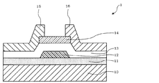
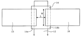
- FIG. 1 is a schematic top view of a field effect transistor 1.
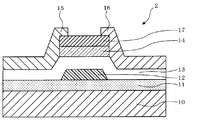
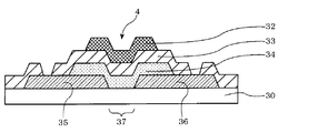
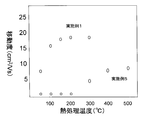
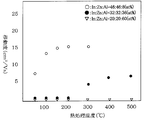
- FIG. It is a schematic sectional drawing of the field effect transistor of other embodiment of this invention. It is a schematic sectional drawing of the field effect transistor of other embodiment of this invention. It is a schematic sectional drawing of the field effect transistor of other embodiment of this invention. It is a schematic sectional drawing of the field effect transistor of other embodiment of this invention. It is a graph which shows the relationship between the heat processing temperature of a semiconductor layer, and a mobility. It is a graph which shows the relationship between the heat processing temperature of a semiconductor layer, and a mobility.
- a field effect transistor having high mobility and low S value can be obtained.
- a field effect transistor with high characteristics can be obtained even with a low-temperature or short-time thermal history (heat treatment).
- the mobility may be lowered, the S value may be increased, the moisture resistance may be lowered, or the chemical resistance to acid / alkali may be lowered. There is.
- the off current and the gate leakage current may be increased, the S value may be increased, the plasma resistance may be decreased, or the threshold may be negative and normally on.
- In / (In + Zn) is preferably 0.3 to 0.75, more preferably 0.35 to 0.7.
- In / (In + X) is preferably 0.45 to 0.98, more preferably 0.65 to 0.98, and particularly preferably 0.7 to 0.97.
- Zn / (X + Zn) is preferably 0.45 to 0.98, more preferably 0.6 to 0.98, and still more preferably 0.7 to 0.97.
- the semiconductor layer further satisfies the following ratio (4) (atomic ratio).
- ratio (4) (atomic ratio).
- X / (In + Zn + X) 0.01 to 0.2 (4) If the ratio of X is greater than 0.2, the S value may increase, the mobility may decrease, and the threshold voltage may increase. On the other hand, if it is less than 0.01, there is a risk that the thermal stability and heat resistance will decrease, the moisture resistance will decrease, the chemical resistance to acids, alkalis, etc. will decrease, and the threshold voltage shift will increase. is there.
- X / (In + Zn + X) is more preferably 0.02 to 0.15, and particularly preferably 0.03 to 0.1.
- the semiconductor layer satisfies the following ratio (5) or (6) (atomic ratio) depending on the application.
- ratio (5) 0.3 to 0.5
- In / (In + Zn + X) 0.5 to 0.7 (not including 0.5) (6)
- the ratio of (5) can easily reduce the off-current and increase the on-off ratio.
- the ratio is (6), the mobility can be increased and the threshold voltage can be decreased.
- the element X is preferably Zr or Hf, and particularly preferably Zr, because the thermal stability, heat resistance, and chemical resistance are improved and the S value and off-current can be reduced.
- the element X is preferably Zr, Hf, Ge, Si, or Ti.
- the element X is preferably Cu, Ni, Co, Fe, Cr, Mn, W, Mo, V, and Nb.
- the field effect transistor of the present invention contains an In (indium) element and a Zn (zinc) element and one or more elements X selected from the following group A in the atomic ratios of (1) to (3) below. It has a semiconductor layer made of a complex oxide.
- a field effect transistor having high mobility and low S value can be obtained.
- a field effect transistor with high characteristics can be obtained even with a low-temperature or short-time thermal history (heat treatment).
- the mobility may be lowered, the S value may be increased, the moisture resistance may be lowered, or the chemical resistance to acid / alkali may be lowered. There is.
- the off current and the gate leakage current may be increased, the S value may be increased, the plasma resistance may be decreased, or the threshold may be negative and normally on.
- In / (In + Zn) is preferably 0.3 to 0.75, more preferably 0.35 to 0.7.
- In / (In + X) is usually 0.29 to 0.99, preferably 0.59 to 0.98, more preferably 0.6 to 0.97, and further preferably 0.65 to 0.96. Particularly preferred is 0.7 to 0.95.
- Zn / (X + Zn) is preferably 0.45 to 0.98, more preferably 0.6 to 0.98, and even more preferably 0. 0.7 to 0.97, particularly preferably 0.75 to 0.90.
- the semiconductor layer further satisfies the following ratio (4) (atomic ratio).
- X / (In + Zn + X) 0.02 to 0.3 (4) If the ratio of X is greater than 0.3, the S value may increase, the mobility may decrease, and the threshold voltage may increase. On the other hand, if it is smaller than 0.02, the thermal stability and heat resistance are lowered, the moisture resistance is lowered, the chemical resistance to acids and alkalis is lowered, the off-current is increased, the threshold voltage is increased. There is a risk of a large shift.
- X / (In + Zn + X) is more preferably 0.04 to 0.25, further preferably 0.055 to 0.2, and particularly preferably 0.06 to 0.15.
- the semiconductor layer satisfy the following ratio (5) or (6) (atomic ratio) because it can be used properly depending on the application.
- ratio (5) 0.3 to 0.5
- In / (In + Zn + X) 0.5 to 0.7 (0.5 is not included) (6)
- the ratio (5) the off-current can be easily reduced and the on-off ratio can be increased.
- the ratio is (6), the mobility can be increased and the threshold voltage can be decreased.
- the element X is preferably Al or B. Also preferred is Sc or Y. Furthermore, lanthanoids (La, Ce, Pr, Nd, Sm, Eu, Gd, Tb, Dy, Ho, Er, Tm, Yb, Lu) are also preferable.
- the field effect transistor of the present invention is not particularly limited as long as it has the semiconductor layer shown in the first aspect or the second aspect described above.
- a known structure such as a top gate type or a bottom gate type can be used.
- a configuration example of a field effect transistor will be described with reference to the drawings.
- FIG. 1 is a schematic cross-sectional view of a field effect transistor according to an embodiment of the present invention.
- the field effect transistor 1 is a bottom gate type, and a gate electrode 12 is formed in a stripe shape on a silicon substrate 10 having a thermal oxide film 11.
- a gate insulating film 13 is provided so as to cover the gate electrode 12, and a semiconductor layer 14 (active layer) is formed on the gate insulating film 13 and on the gate electrode 12.
- a source electrode 15 is connected to one end 14 a of the semiconductor layer 14 in a direction orthogonal to the gate electrode 12. Further, the drain electrode 16 is connected to the other end 14 b facing the one end 14 a of the semiconductor layer 14.
- FIG. 2 is a schematic top view showing the positional relationship between the gate electrode 12, the semiconductor layer 14, the source electrode 15, and the drain electrode 16. Some members are omitted for visualization of the positional relationship.
- the semiconductor layer is preferably protected by a protective layer.
- a protective layer In the case of a bottom gate type transistor, if there is no protective layer, the main part of the semiconductor layer is exposed, so the effect of the protective layer is great.
- 3 and 4 are schematic cross-sectional views of a field effect transistor according to another embodiment of the present invention.
- the field effect transistors 2 and 3 have the same configuration as the field effect transistor 1 described above except that the protective layer 17 is formed.
- FIG. 5 is a schematic cross-sectional view illustrating an example of a top gate type field effect transistor.
- a source electrode 35 and a drain electrode 36 are formed on a substrate 30, and a semiconductor layer 34 is provided so as to cover the gap and part of these electrodes.
- a gate electrode 32 is formed on the semiconductor layer 34 via a gate insulating film 33.
- the substrate 30 serves as the protective layer 37.
- Substrate there is no particular limitation, and those known in this technical field can be used.
- glass substrates such as alkali silicate glass, non-alkali glass and quartz glass, silicon substrates, resin substrates such as acrylic, polycarbonate and polyethylene naphthalate (PEN), polymer film bases such as polyethylene terephthalate (PET) and polyamide Materials can be used.
- the thickness of the substrate or base material is generally 0.1 to 10 mm, preferably 0.3 to 5 mm.
- a glass substrate those chemically or thermally reinforced are preferred.
- a glass substrate and a resin substrate are preferable, and a glass substrate is particularly preferable.
- weight reduction is required, a resin substrate or a polymer material is preferable.
- the semiconductor layer contains In (indium), Zn (zinc) and the element X shown in the first aspect or the second aspect described above in a ratio of (1) to (3), preferably (1) to It consists of the complex oxide contained so that the ratio of (4) may be satisfy
- Such a semiconductor layer can be produced, for example, by forming a thin film using the complex oxide target (target for semiconductor layer) of the present invention.
- the target for a semiconductor layer of the present invention is composed of a composite oxide sintered body satisfying the ratios (1) to (3) or (1) to (4) shown in the first aspect or the second aspect.
- the target is made of, for example, a mixed powder containing indium oxide, zinc oxide, and an oxide of element X so as to satisfy the above element ratio.
- the raw material powder can be produced by finely pulverizing with a ball mill or the like, then forming into a target and firing.
- a part of raw material powder to be used may be one obtained by collecting from high-purity indium oxide-containing scrap such as target scraps and used targets.
- indium oxide recovered from the ITO target preferably contains Sn (tin) as an impurity.
- Indium oxide can be recovered by a known method such as the method described in JP-A No. 2002-069544.
- the element X shown in the first aspect is Zr, Hf, Ge, Si, Ti, V, and Nb, it is easy to manufacture a target having a particularly good appearance and high bending strength.
- the purity of each raw material powder is usually 99.9% (3N) or higher, preferably 99.99% (4N) or higher, more preferably 99.995% or higher, particularly preferably 99.999% (5N) or higher. . If the purity of each raw material powder is less than 99.9% (3N), the semiconductor characteristics may be deteriorated due to impurities, appearance defects such as uneven color and spots may occur, and reliability may be reduced. is there.
- the specific surface area of the indium oxide powder is 8 to 10 m 2 / g
- the specific surface area of the zinc oxide powder is 2 to 4 m 2 / g
- the specific surface area of the oxide of the element X is 5 to 10 m 2 / g (more preferably Is preferably 8 to 10 m 2 / g).
- the median diameter of the indium oxide powder is preferably 0.2 to 2 ⁇ m
- the median diameter of the zinc oxide powder is preferably 0.8 to 1.6 ⁇ m.
- the difference in specific surface area is preferably 5 m 2 / g or less. If the specific surface area is too different, efficient pulverization and mixing cannot be performed, and oxide particles of the element X may remain in the sintered body.
- the mixed powder is mixed and ground using, for example, a wet medium stirring mill.
- the specific surface area after pulverization is increased by 1.5 to 2.5 m 2 / g from the specific surface area of the raw material mixed powder, or is pulverized so that the average median diameter after pulverization is 0.6 to 1 ⁇ m. It is preferable to do.
- a high-density oxide sintered body can be obtained without requiring a calcination step at all. Moreover, a reduction process is also unnecessary.
- the increase in the specific surface area of the raw material mixed powder is less than 1.0 m 2 / g or the average median diameter of the raw material mixed powder after pulverization exceeds 1 ⁇ m, the sintered density may not be sufficiently increased.
- the increase in the specific surface area of the raw material mixed powder exceeds 3.0 m 2 / g, or if the average median diameter after pulverization is less than 0.6 ⁇ m, contamination from the pulverizer during pulverization (impurity contamination amount) ) May increase.
- the specific surface area of each powder is a value measured by the BET method.
- the median diameter of the particle size distribution of each powder is a value measured with a particle size distribution meter.
- These values can be adjusted by pulverizing the powder by a dry pulverization method, a wet pulverization method or the like.
- the raw material after the pulverization step is dried with a spray dryer or the like and then molded.
- a known method such as pressure forming or cold isostatic pressing can be employed.
- the obtained molded product is sintered to obtain a sintered body.
- Sintering is preferably performed at 1350 to 1600 ° C. for 2 to 20 hours. When the temperature is lower than 1350 ° C., the density is not improved. When the temperature exceeds 1600 ° C., zinc is evaporated, the composition of the sintered body is changed, or voids (voids) are generated in the sintered body due to the evaporation. There is. Sintering is preferably performed in an oxygen atmosphere by circulating oxygen or under pressure. Thereby, transpiration of zinc can be suppressed, and a sintered body free from voids (voids) can be obtained. Since the sintered body manufactured in this manner has a high density and generates less nodules and particles during use, an oxide semiconductor film having excellent film characteristics can be manufactured.
- the oxide sintered body becomes a target by performing processing such as polishing.
- the sintered body is ground by, for example, a surface grinder so that the surface roughness Ra is 5 ⁇ m or less.
- the sputter surface of the target may be mirror-finished so that the average surface roughness Ra is 1000 angstroms or less.
- a known polishing technique such as mechanical polishing, chemical polishing, mechanochemical polishing (a combination of mechanical polishing and chemical polishing) can be used.
- polishing to # 2000 or more with a fixed abrasive polisher polishing liquid: water
- lapping with loose abrasive lapping abrasive: SiC paste, etc.
- lapping by changing the abrasive to diamond paste can be obtained by:
- Such a polishing method is not particularly limited.
- the film forming method include a sputtering method, a PLD (pulse laser deposition) method, a vacuum deposition method, and an ion plating method.
- cleaning, etc. can be used for the cleaning process of a target.
- cleaning, etc. can be used for the cleaning process of a target.
- ultrasonic cleaning and the like can also be performed.
- a method of performing multiple oscillation at a frequency of 25 to 300 KHz is effective.
- the particle size of each compound in the oxide sintered body is preferably 20 ⁇ m or less, more preferably 10 ⁇ m or less, and particularly preferably 5 ⁇ m or less.
- the particle size is an average particle size measured with an electron probe microanalyzer (EPMA).
- the crystal grain size is, for example, the raw material indium oxide, the oxide of X element, the blending ratio of each powder of zinc oxide, the grain size of the raw material powder, the purity, the temperature rise time, the sintering temperature, the sintering time, It is obtained by adjusting the sintering atmosphere and the temperature lowering time. If the particle size of the compound is larger than 20 ⁇ m, nodules may be generated during sputtering.
- the density of the target is preferably 95% or more of the theoretical density, more preferably 98% or more, and particularly preferably 99% or more. If the density of the target is less than 95%, the strength is insufficient and the target may be damaged during film formation. In addition, performance may be uneven when a transistor is manufactured.
- the theoretical relative density of the target is the specific gravity of each oxide (for example, ZnO is 5.66 g / cm 3 , In 2 O 3 is 7.12 g / cm 3 , and ZrO 2 is 5.98 g / cm 3 ). The density is calculated from the quantitative ratio, and the ratio with the density measured by the Archimedes method is calculated to obtain the theoretical relative density.
- the target bulk resistance is preferably 20 m ⁇ or less, more preferably 10 m ⁇ or less, further preferably 5 m ⁇ or less, and particularly preferably 2 m ⁇ cm or less. . If it is greater than 20 m ⁇ , the target may be damaged during film formation by DC sputtering. In addition, a spark may be generated due to abnormal discharge, and the target may be cracked, or particles ejected by the spark may adhere to the deposition substrate and deteriorate the performance as an oxide semiconductor film. In addition, the target may break during discharge.
- the bulk resistance is a value measured by a four-probe method using a resistivity meter.
- the bending strength of the target of the present invention is preferably 8 kg / mm 2 or more, more preferably 10 kg / mm 2 or more, and particularly preferably 12 kg / mm 2 or more.
- the target is required to have a certain level of bending force because a load is applied during transportation and mounting of the target, and the target may be damaged. If the target is less than 8 kg / mm 2 , it cannot be used as a target. There is a fear.
- the bending strength of the target can be measured according to JIS R 1601.
- the target relating to the second aspect of the present invention is further selected from the group consisting of Sn (tin), Ge (germanium), Si (silicon), Ti (titanium), Zr (zirconium) and Hf (hafnium). It is preferable to contain 100 to 10,000 ppm of one or more elements. When these elements are included, the target density is improved, the strength is increased, the resistance is decreased, the color unevenness is decreased, the uniformity is improved, the abnormal discharge and the yellow flakes are decreased, and the quality as a semiconductor target is improved. It can be expected to improve.
- the above elements may be contained as impurities using raw materials recovered from a sintered body (target) containing these elements. Moreover, you may add to a raw material as a metal powder or an oxide.
- the semiconductor layer is preferably an amorphous film.
- an amorphous film By being an amorphous film, adhesion to an insulating film and a protective layer is improved, and uniform transistor characteristics can be easily obtained even in a large area.
- whether the semiconductor layer is an amorphous film can be confirmed by X-ray crystal structure analysis. The case where no clear peak is observed is amorphous.
- the electron carrier concentration of the semiconductor layer is preferably 10 13 to 10 18 / cm 3 , particularly preferably 10 14 to 10 17 / cm 3 .
- the band gap is preferably 2.0 to 6.0 eV, and more preferably 2.8 to 5.0 eV. If the band gap is smaller than 2.0 eV, visible light is absorbed and the field effect transistor may malfunction. On the other hand, if it is larger than 6.0 eV, it is difficult to supply carriers and the field effect transistor may not function.
- the semiconductor layer is preferably a non-degenerate semiconductor exhibiting a thermal activation type. If the semiconductor is a degenerate semiconductor, there are too many carriers, which may increase the off-current / gate leakage current, or the threshold value may become negative, resulting in normally-on. Whether the semiconductor layer is a non-degenerate semiconductor can be determined by measuring temperature changes in mobility and carrier density using the Hall effect. In addition, the semiconductor layer can be a non-degenerate semiconductor by adjusting the oxygen partial pressure during film formation or by performing post-processing to control the amount of oxygen defects and optimize the carrier density.
- the surface roughness (RMS) of the semiconductor layer is preferably 1 nm or less, more preferably 0.6 nm or less, and particularly preferably 0.3 nm or less. If it is larger than 1 nm, the mobility may decrease.
- the semiconductor layer is preferably an amorphous film that maintains at least part of the edge sharing structure of the bixbite structure of indium oxide. Whether or not the amorphous film containing indium oxide maintains at least a part of the edge sharing structure of the bixbite structure of indium oxide is determined by small angle incident X-ray scattering (GIXS) using high-intensity synchrotron radiation or the like. From the radial distribution function (RDF) obtained by the above, it can be confirmed that the peak representing In—X (X is In, Zn) is between 0.30 and 0.36 nm. For details, the following documents may be referred to. F. Utsuno, et al. , Thin Solid Films, Volume 496, 2006, Pages 95-98
- a / B> 0.7 is preferably satisfied, A / B> 0.85 is more preferable, A / B> 1 is further more preferable, and A / B> 1.2 is particularly preferable.
- a / B is 0.7 or less, when a semiconductor layer is used as an active layer of a transistor, there is a possibility that the mobility may decrease or the threshold value or S value may become too large. It is considered that the small A / B reflects the poor short-range order of the amorphous film.
- the average In—In bond distance is preferably 0.3 to 0.322 nm, particularly preferably 0.31 to 0.32 nm.
- the average bond distance of In—In can be determined by X-ray absorption spectroscopy.
- the measurement by X-ray absorption spectroscopy shows an X-ray absorption wide-area microstructure (EXAFS) that has spread to a high energy as high as several hundred eV from the rise.
- EXAFS is caused by backscattering of electrons by atoms around the excited atom. Interference effect between the flying electron wave and the back-scattered wave occurs. Interference depends on the wavelength of the electronic state and the optical path length to and from surrounding atoms.
- a radial distribution function (RDF) is obtained by Fourier transforming EXAFS.
- the average bond distance can be estimated from the RDF peak.
- the film thickness of the semiconductor layer is usually 0.5 to 500 nm, preferably 1 to 150 nm, more preferably 3 to 80 nm, and particularly preferably 10 to 60 nm. If it is thinner than 0.5 nm, it is difficult to form a uniform film industrially. On the other hand, if it is thicker than 500 nm, the film formation time becomes long and cannot be adopted industrially. When the thickness is in the range of 3 to 80 nm, TFT characteristics such as mobility and on / off ratio are particularly good.
- the semiconductor layer is preferably an amorphous film, and the energy width (E 0 ) of the delocalized level is preferably 14 meV or less.
- the energy width (E 0 ) of the delocalized level of the semiconductor layer is more preferably 10 meV or less, further preferably 8 meV or less, and particularly preferably 6 meV or less.
- the energy width (E 0 ) of the delocalized level is larger than 14 meV, when the semiconductor layer is used as the active layer of the transistor, the mobility may be lowered or the threshold value or the S value may be too large. It is considered that the large energy width (E 0 ) of the delocalized level of the semiconductor layer reflects the poor short-range order of the amorphous film.
- the field effect transistor preferably has a protective layer of semiconductor. Without the semiconductor protective layer, oxygen in the surface layer of the semiconductor is desorbed in a vacuum or under a low pressure, which may increase the off-current or make the threshold voltage negative. Further, even in the atmosphere, there is a risk that variations in transistor characteristics such as threshold voltage may increase due to the influence of surroundings such as humidity.
- the material for forming the semiconductor protective layer is not particularly limited. What is generally used can be arbitrarily selected as long as the effects of the present invention are not lost.
- SiO 2, SiNx, Al 2 O 3, Ta 2 O 5, TiO 2, MgO, ZrO 2, CeO 2, K 2 O, Li 2 O, Na 2 O, Rb 2 O, Sc 2 O 3, Y 2 O 3 , Hf 2 O 3 , CaHfO 3 , PbTi 3 , BaTa 2 O 6 , SrTiO 3 , AlN, or the like can be used.
- the number of oxygen in these oxides does not necessarily match the stoichiometric ratio (for example, it may be SiO 2 or SiO x).
- SiNx may contain a hydrogen element.
- Such a protective film may have a structure in which two or more different insulating films are stacked.
- the protective layer may be crystalline, polycrystalline, or amorphous, but is preferably polycrystalline or amorphous that is easy to produce industrially. However, it is particularly preferred that the protective layer is amorphous. If it is not an amorphous film, the smoothness of the interface is poor, and the mobility may be lowered, or the threshold voltage and S value may be too large.
- the protective layer of the semiconductor layer is preferably an amorphous oxide or an amorphous nitride, and particularly preferably an amorphous oxide. Further, if the protective layer is not an oxide, oxygen in the semiconductor moves to the protective layer side, and there is a possibility that the off current becomes high or the threshold voltage becomes negative and normally off. Further, an organic insulating film such as poly (4-vinylphenol) (PVP) or parylene may be used for the protective layer of the semiconductor layer. Further, the protective layer of the semiconductor layer may have a laminated structure of two or more layers of an inorganic insulating film and an organic insulating film.
- Gate insulating film There is no particular limitation on the material for forming the gate insulating film. What is generally used can be arbitrarily selected as long as the effects of the invention of the present embodiment are not lost. For example, SiO 2, SiNx, Al 2 O 3, Ta 2 O 5, TiO 2, MgO, ZrO 2, CeO 2, K 2 O, Li 2 O, Na 2 O, Rb 2 O, Sc 2 O 3, Y 2 O 3 , Hf 2 O 3 , CaHfO 3 , PbTi 3 , BaTa 2 O 6 , SrTiO 3 , AlN, or the like can be used.
- the number of oxygen in these oxides does not necessarily match the stoichiometric ratio (for example, it may be SiO 2 or SiO x).
- SiNx may contain a hydrogen element.
- Such a gate insulating film may have a structure in which two or more different insulating films are stacked.
- the gate insulating film may be crystalline, polycrystalline, or amorphous, but is preferably polycrystalline or amorphous that is easy to manufacture industrially.
- the gate insulating film may be an organic insulating film such as poly (4-vinylphenol) (PVP) or parylene. Further, the gate insulating film may have a stacked structure of two or more layers of an inorganic insulating film and an organic insulating film.
- Electrode There are no particular limitations on the material for forming each of the gate electrode, the source electrode, and the drain electrode, and any material generally used can be selected as long as the effects of the present invention are not lost.
- transparent electrodes such as indium tin oxide (ITO), indium zinc oxide, ZnO, SnO 2 , metal electrodes such as Al, Ag, Cr, Ni, Mo, Au, Ti, Ta, Cu, or these An alloy metal electrode can be used.
- ITO indium tin oxide
- ZnO zinc oxide
- SnO 2 zinc oxide
- metal electrodes such as Al, Ag, Cr, Ni, Mo, Au, Ti, Ta, Cu, or these
- the resistance of the interface with the semiconductor electrode may be adjusted by plasma treatment, ozone treatment or the like.
- the manufacturing method of the present invention includes a step of forming a semiconductor layer by DC or AC sputtering using the above-described target of the present invention, and a step of heat-treating at 70 to 350 ° C. after forming the semiconductor layer, To do.
- Each constituent member (layer) of the above-described field effect transistor can be formed by a method known in this technical field. Specifically, as a film formation method, a chemical film formation method such as a spray method, a dip method, or a CVD method, or a physical film formation method such as a sputtering method, a vacuum evaporation method, an ion plating method, or a pulse laser deposition method. The method can be used. Since the carrier density is easily controlled and the film quality can be easily improved, a physical film formation method is preferably used, and a sputtering method is more preferably used because of high productivity.
- a method using a sintered complex oxide target In sputtering, a method using a sintered complex oxide target, a method using co-sputtering using a plurality of sintered targets, a method using reactive sputtering using an alloy target, and the like can be used.
- the uniformity and reproducibility are deteriorated, or the energy width of delocalized levels (E 0 ) May increase, and the transistor characteristics may be deteriorated, for example, the mobility may be decreased or the threshold voltage may be increased.
- a composite oxide sintered target is used.
- the formed film can be patterned by various etching methods.
- the semiconductor layer is formed by DC or AC sputtering using the target of the present invention.
- DC or AC sputtering damage during film formation can be reduced as compared with RF sputtering. For this reason, in the field effect transistor, effects such as a reduction in threshold voltage shift, an improvement in mobility, a reduction in threshold voltage, and a reduction in S value can be expected.
- heat treatment is performed at 70 to 350 ° C. If it is lower than 70 ° C., the thermal stability and heat resistance of the obtained transistor may be lowered, the mobility may be lowered, the S value may be increased, or the threshold voltage may be increased. On the other hand, when the temperature is higher than 350 ° C., a substrate having no heat resistance may not be used, the cost of heat treatment equipment may be increased, the interface of the protective layer, the insulating film, or the semiconductor layer may be deteriorated, or the moisture pressure may be lowered. When the film is formed, it may crystallize and an amorphous film may not be obtained.
- the heat treatment temperature is preferably 80 to 260 ° C, more preferably 90 to 180 ° C, and further preferably 100 to 150 ° C.
- a heat treatment temperature of 180 ° C. or lower is preferable because a resin substrate having low heat resistance such as PEN can be used as the substrate.
- the heat treatment time is usually preferably 1 second to 24 hours, but is preferably adjusted according to the treatment temperature. For example, at 70 to 180 ° C., 10 minutes to 24 hours are more preferable, 20 minutes to 6 hours are more preferable, and 30 minutes to 3 hours are particularly preferable. At 180 to 260 ° C., 6 minutes to 4 hours is more preferable, and 15 minutes to 2 hours is more preferable. At 260 to 300 ° C., 30 seconds to 4 hours is more preferable, and 1 minute to 2 hours is particularly preferable. At 300 to 350 ° C., 1 second to 1 hour is more preferable, and 2 seconds to 30 minutes is particularly preferable.
- the heat treatment is preferably performed in an inert gas in an environment where the oxygen partial pressure is 10 ⁇ 3 Pa or less, or after the semiconductor layer is covered with a protective layer. Reproducibility is improved under the above conditions.
- the inert gas N 2 , He, Ne, Ar, Kr, and Xe are preferable.
- the field effect transistor of the present invention mobility is preferably at least 1 cm 2 / Vs, more preferably at least 3 cm 2 / Vs, particularly preferably at least 8 cm 2 / Vs. If it is smaller than 1 cm 2 / Vs, the switching speed becomes slow, and there is a possibility that it cannot be used for a large-screen high-definition display.
- the on / off ratio is preferably 10 6 or more, more preferably 10 7 or more, and particularly preferably 10 8 or more.
- the off current is preferably 2 pA or less, more preferably 1 pA or less, further preferably 0.5 pA or less, and particularly preferably 0.2 pA or less.
- the gate leakage current is preferably 1 pA or less. If it is larger than 1 pA, the contrast may deteriorate when used as a TFT of a display.
- the threshold voltage is usually 0 to 10V, preferably 0 to 4V, more preferably 0 to 3V, and particularly preferably 0 to 2V. If it is less than 0V, it is normally on, and it is necessary to apply a voltage when it is off, which may increase power consumption. If it is greater than 10V, the drive voltage may increase and the power consumption may increase, or high mobility may be required.
- the S value is preferably 0.8 V / dec or less, more preferably 0.3 V / dec or less, further preferably 0.25 V / dec or less, and particularly preferably 0.2 V / dec or less. If it is greater than 0.8 V / dec, the drive voltage may increase and power consumption may increase. In particular, when used in an organic EL display, it is preferable to set the S value to 0.3 V / dec or less because of direct current drive because power consumption can be greatly reduced.
- the S value is a value indicating the steepness of the drain current that rises sharply from the off state to the on state when the gate voltage is increased from the off state.
- S value dVg / dlog (Ids)
- the smaller the S value, the sharper the rise (All about Thin Film Transistor Technology", Ikuhiro Ukai, 2007, Industrial Research Committee).
- the S value is large, it is necessary to apply a high gate voltage when switching from on to off, and power consumption may increase.
- the shift amount of the threshold voltage before and after being applied for 100 hours at a DC voltage of 10 ⁇ A at 50 ° C. is preferably 1.0 V or less, and more preferably 0.5 V or less. If it is greater than 1V, the image quality may change when used as a transistor in an organic EL display.
- the hysteresis when the gate voltage is raised and lowered by the transfer curve is small.
- the ratio W / L of the channel width W to the channel length L is usually 0.1 to 100, preferably 0.5 to 20, and particularly preferably 1 to 8. If W / L exceeds 100, the leakage current may increase or the on-off ratio may decrease. If it is less than 0.1, the field effect mobility may be lowered, or pinch-off may be unclear.
- the channel length L is usually 0.1 to 1000 ⁇ m, preferably 1 to 100 ⁇ m, more preferably 2 to 10 ⁇ m. If the thickness is 0.1 ⁇ m or less, it is difficult to produce industrially and the leakage current may be increased. If the thickness is 1000 ⁇ m or more, the device becomes too large, which is not preferable.
- the field effect transistor of the present invention preferably has a structure for shielding the semiconductor layer. If the semiconductor layer does not have a structure that shields light (for example, a light shielding layer), when electrons enter the semiconductor layer, carrier electrons may be excited and off current may be increased.
- the light shielding layer is preferably a thin film having absorption at 300 to 800 nm.
- the light shielding layer may be either the upper part or the lower part of the semiconductor layer, but is preferably on both the upper part and the lower part. Further, the light shielding layer may also be used as a gate insulating film, a black matrix, or the like. When the light shielding layer is on only one side, it is necessary to devise a structure so that light is not irradiated to the semiconductor layer from the side where the light shielding layer is not present.
- the contact layer it is preferable to provide a contact layer between the semiconductor layer and the source or drain electrode.
- a material for forming the contact layer a composite oxide having the same composition as that of the semiconductor layer described above can be used. That is, the contact layer is preferably an oxide whose main component is an element contained in the semiconductor layer, such as In or Zn. If these elements are not included, element movement occurs between the contact layer and the semiconductor layer, and the threshold voltage may shift significantly when a stress test or the like is performed.
- a contact layer having the same composition ratio as the semiconductor layer can be formed by changing the film formation conditions, a layer having a composition ratio different from that of the semiconductor layer can be formed, or a semiconductor electrode
- the contact portion may be formed by increasing the resistance by plasma treatment or ozone treatment, or a layer having a higher resistance may be formed by film formation conditions such as oxygen partial pressure when forming the semiconductor layer.
- an oxide resistance layer having higher resistance than the semiconductor layer is provided between the semiconductor layer and the gate insulating film and / or between the semiconductor layer and the protective layer. . If the oxide resistance layer is not provided, off current may be generated, or the threshold voltage may be negative and normally on. Further, the semiconductor layer may be altered during the post-treatment process such as protective film formation or etching, and the characteristics may be deteriorated.
- the following can be illustrated as an oxide resistance layer.
- ⁇ Amorphous oxide film with the same composition as the semiconductor layer deposited at a higher oxygen partial pressure than when the semiconductor film was deposited ⁇ Amorphous oxide film with the same composition as the semiconductor layer but with a different composition ratio
- An amorphous oxide film containing In and Zn and containing an element X different from the semiconductor layer a polycrystalline oxide film containing indium oxide as a main component.
- Indium oxide as a main component Zn, Cu, Co, Ni, Mn
- the composition contained in the polycrystalline oxide film / semiconductor layer doped with one or more positive divalent elements such as Mg is further selected from Cu, Co, Ni, Mn, Fe, Mg, Ca, Sr, Ba, Ag, Au Amorphous oxide film with one or more elements added
- the In composition ratio is the semiconductor layer. Is preferably less. Moreover, it is preferable that the composition ratio of the element X is larger than that of the semiconductor layer.
- the oxide resistance layer is preferably an oxide containing each element of In and Zn. If these elements are not included, element movement occurs between the oxide resistance layer and the semiconductor layer, and the threshold voltage may shift significantly when a stress test or the like is performed.
- an amorphous oxide film in which one or more elements selected from Cu, Co, Ni, Mn, Fe, Mg, Ca, Sr, Ba, Ag, Au are added to the composition contained in the semiconductor layer
- the In composition ratio is preferably smaller than that of the semiconductor layer.
- Example 1 Production of sputtering target As raw materials, powders of indium oxide, zinc oxide and zirconium oxide have an atomic ratio [In / (In + Zn + Zr)] of 0.48 and an atomic ratio [Zn / (In + Zn + Zr)] of 0.50. Mixing was performed so that the atomic ratio [Zr / (In + Zn + Zr)] was 0.02. This was supplied to a wet ball mill and mixed and ground for 72 hours to obtain a raw material fine powder. After granulating the obtained raw material fine powder, it was press-molded to a size of 10 cm in diameter and 5 mm in thickness, put in a firing furnace and fired at 1500 ° C.
- the target had a bulk resistance of 3 m ⁇ and a theoretical relative density of 0.99.
- the theoretical relative density was obtained by calculating the ratio of the density calculated from the specific gravity of each oxide and the amount ratio thereof to the density measured by the Archimedes method.
- the target manufactured in (1) is mounted on a DC magnetron sputtering film forming apparatus, which is one of the DC sputtering methods, formed on the gate insulating film, and then patterned to form a semiconductor layer (film thickness). 50 nm).
- Sputtering conditions are: substrate temperature: 25 ° C., ultimate pressure: 1 ⁇ 10 ⁇ 6 Pa, atmospheric gas: Ar 99.5% and oxygen 0.5%, sputtering pressure (total pressure): 2 ⁇ 10 ⁇ 1 Pa, input power The distance was 100 W, the film formation time was 6 minutes, and the ST distance was 110 mm.
- a source / drain electrode made of In 2 O 3 —ZnO was formed using a lift-off process and RF magnetron sputtering (room temperature, Ar 100%). Thereafter, a field effect transistor was manufactured by heat treatment at 170 ° C. for 2 hours in a nitrogen environment (a bottom-gate field effect transistor having W of 40 ⁇ m and L of 4 ⁇ m in FIG. 2).
- a semiconductor layer was formed on the glass substrate (Corning 1737) using the target manufactured in Example (1) and evaluated.
- the semiconductor layer was formed in the same manner as in Example (2) using a DC magnetron sputtering film forming apparatus. As a result, an oxide thin film having a thickness of 50 nm was formed on the glass substrate.
- the atomic ratio [In / (In + Zn + Zr)] was 0.49
- the atomic ratio [Zn / (In + Zn + Zr)] was 0.49
- the atomic ratio [Ga / (In + Zn + Zr)] was 0.02.
- the semiconductor film was heat-treated at 170 ° C. for 2 hours in a nitrogen environment.
- the carrier concentration and hole mobility of the semiconductor film after the heat treatment were measured with a hole measuring device.
- the result was n-type, the carrier concentration was 4 ⁇ 10 17 cm ⁇ 3 , and the hole mobility was 2 cm 2 / Vs.
- the Hall measuring device and the measurement conditions were as follows: ⁇ Hall measuring device manufactured by Toyo Technica: Resi Test 8310 ⁇ Measurement conditions Measurement temperature: Room temperature (25 °C) Measurement magnetic field: 0.5T Measurement current: 10 ⁇ 12 to 10 ⁇ 4 A Measurement mode: AC magnetic field hall measurement
- the surface roughness measured by AMF was RMS 0.2 nm.
- the band gap obtained optically was 3.8 eV.
- the Hall effect was measured by changing the measurement temperature in the range of 77 to 300K, it was confirmed that the semiconductor film was a non-degenerate semiconductor.
- the energy width (E 0 ) of the delocalized level was 6 meV or less from the relationship between the carrier concentration and the activation energy measured using the Hall effect while changing the temperature.
- a radial distribution function (RDF) obtained by X-ray scattering measurement confirmed that a peak representing In—In was observed at around 0.35 nm, and a ridge sharing structure of the bixbite structure of indium oxide remained. did it.
- a / B where A is the maximum value of RDF with an interatomic distance of 0.30 to 0.36 nm, and B is the maximum value of RDF with an interatomic distance of 0.36 to 0.42.
- the average In—In bond distance determined by X-ray absorption spectroscopy was 0.318 nm.
- Acid resistance and moisture resistance were evaluated as follows.
- the resistance before and after the test was measured and classified as follows.
- the rate of change was defined as the resistance value before the test divided by the resistance value after the test or the resistance value after the test divided by the resistance value before the test.
- ⁇ Change rate less than 2 times
- ⁇ Change rate 2 to 5 times change
- ⁇ Change rate 5 to 100 times change
- Table 1 shows the measurement results.
- Example 2 Comparative Examples 1 to 7
- a sputtering target was manufactured in the same manner as in Example 1 (1) except that the mixing ratio of the raw materials, indium oxide, zinc oxide, and X element oxide was adjusted to the composition shown in Table 1-4.
- a field effect transistor was fabricated and evaluated in the same manner as in Example 1 (2) except that the above sputtering target was used and the film formation conditions were changed as shown in Table 1-4.
- the raw materials used in place of zirconium oxide when manufacturing the sputtering target are as follows.
- Example 12 HfO 2 , manufactured by Kojundo Chemical Laboratory Co., Ltd., HFO01PB
- Example 13 GeO 2 , GEO06PB manufactured by Kojundo Chemical Laboratory Co., Ltd.
- Example 14 SiO 2 , manufactured by Kojundo Chemical Laboratory Co., Ltd., SIO12PB
- Example 15 TiO 2 , manufactured by Kojundo Chemical Laboratory Co., Ltd., TIO14PB
- Example 16 MnO 2 , manufactured by Kojundo Chemical Laboratory Co., Ltd., MNO03PB
- Example 17 WO 3, Kojundo Chemical Laboratory Co., Ltd.
- Example 18 MoO 3 , manufactured by Kojundo Chemical Laboratory Co., Ltd., MOO03PB
- Example 19 V 2 O 5 , manufactured by Kojundo Chemical Laboratory Co., Ltd., VVO09PB
- Example 20 Nb 2 O 5 , manufactured by Kojundo Chemical Laboratory Co., Ltd., NBO08PB
- Example 25 CuO, manufactured by Kojundo Chemical Laboratory Co., Ltd., CUO08PB
- Example 26 NiO, manufactured by Kojundo Chemical Laboratory Co., Ltd., NIO11PB
- Example 27 CoO, manufactured by Kojundo Chemical Laboratory Co., Ltd., COO03PB
- Example 28 FeO, manufactured by Kojundo Chemical Laboratory Co., Ltd., FEO01PB
- Example 29 Cr 2 O 3 , manufactured by Kojundo Chemical Laboratory Co., Ltd., CRO01GB
- Example 21 after forming the source / drain electrodes, a protective layer was formed by forming 300 nm of SiO 2 by RF magnetron sputtering to produce the field effect transistor shown in FIG.
- Example 22 and Comparative Examples 1 to 7 the semiconductor layer was formed by RF sputtering.
- the target was mounted on an RF magnetron sputtering film forming apparatus to form a film.
- the sputtering conditions here are: substrate temperature: 25 ° C., ultimate pressure: 1 ⁇ 10 ⁇ 6 Pa, atmospheric gas: Ar 99.5% and oxygen 0.5%, sputtering pressure (total pressure); 2 ⁇ 10 ⁇ 1 Pa
- the input power was 100 W
- the film formation time was 8 minutes
- the ST distance was 100 mm.
- Example 23 a silicon substrate with a SiO 2 thermal oxide film was used. The thickness of the SiO 2 thermal oxide film was 100 nm.
- the gate insulating film is a SiO 2 thermal oxide film, and the silicon substrate serves as a gate electrode and a substrate.
- a semiconductor layer, a source electrode, and a drain electrode were formed in the same manner as in Example 1 on a silicon substrate with a SiO 2 thermal oxide film.
- Example 30 As raw materials, powders of indium oxide, zinc oxide and zirconium oxide have an atomic ratio [In / (In + Zn + Zr)] of 0.4, an atomic ratio [Zn / (In + Zn + Zr)] of 0.4, and an atomic ratio [Zr / (In + Zn + Zr). )] was 0.2. This was supplied to a wet ball mill and mixed and ground for 72 hours to obtain a raw material fine powder. After granulating the obtained raw material fine powder, it was press-molded to a size of 20 cm in diameter and 5 mm in thickness, and then placed in a firing furnace and fired at 1400 ° C.
- the target had a bulk resistance of 5 m ⁇ and a theoretical relative density of 0.98.
- the target bending strength was 12 kg / mm 2 .
- a target having no color unevenness and high appearance uniformity was obtained.
- Comparative Example 8 As raw materials, powders of indium oxide, zinc oxide and gallium oxide have an atomic ratio [In / (In + Zn + Ga)] of 0.4, an atomic ratio [Zn / (In + Zn + Ga)] of 0.4, and an atomic ratio [Ga / (In + Zn + Ga). )] was 0.2. This was supplied to a wet ball mill and mixed and ground for 72 hours to obtain a raw material fine powder. After granulating the obtained raw material fine powder, it was press-molded to a size of 20 cm in diameter and 5 mm in thickness, and then placed in a firing furnace and fired at 1400 ° C. for 12 hours to obtain a sintered body (target). It was. The target had a bulk resistance of 70 m ⁇ and a theoretical relative density of 0.82. The target bending strength was 7 kg / mm 2 . In addition, slight uneven color was confirmed on the target.
- FIG. 6 shows the relationship between the heat treatment temperature and the mobility of the semiconductor layer having the same composition as in Examples 1 and 5.
- the processing time is 2 hours.
- the mobility was stabilized by treatment at 150 ° C., whereas in the composition of Example 5, a treatment temperature of 300 ° C. or more was required to stabilize the mobility.
- Example 31 [Second embodiment] [Production of sputtering target]
- Example 31 (Target I)
- 5N purity 99.999%) indium oxide (INO04PB manufactured by Kojundo Chemical Laboratory Co., Ltd.), 5N zinc oxide (ZNO04PB manufactured by Kojundo Chemical Laboratory Co., Ltd.) and 5N aluminum oxide (stock) Company high purity chemical research laboratory company) powder
- atomic ratio [In / (In + Zn + Al)] is 0.48
- atomic ratio [Zn / (In + Zn + Al)] is 0.50
- atomic ratio [Al / (In + Zn + Al)] was mixed to 0.02. This was supplied to a wet ball mill and mixed and ground for 72 hours to obtain a raw material fine powder.
- the target After granulating the obtained raw material fine powder, it is press-molded to a size of 10 cm in diameter and 5 mm in thickness, put in a firing furnace and fired at 1500 ° C. for 12 hours to obtain a sintered body (target). It was.
- impurities such as Sn (tin), Ge (germanium), Si (silicon), Ti (titanium), Zr (zirconium), and Hf (hafnium) were not contained. Further, the target had a bulk resistance of 20 m ⁇ and a theoretical relative density of 0.95.
- Example 32 Powders of indium oxide, 5N zinc oxide (ZNO04PB manufactured by Kojundo Chemical Laboratory Co., Ltd.) and 4N aluminum oxide (ALO12PB manufactured by Kojundo Chemical Laboratory Co., Ltd.) recovered from used ITO targets as raw materials Were mixed so that the atomic ratio [In / (In + Zn + Al)] was 0.48, the atomic ratio [Zn / (In + Zn + Al)] was 0.50, and the atomic ratio [Al / (In + Zn + Al)] was 0.02. This was supplied to a wet ball mill and mixed and ground for 72 hours to obtain a raw material fine powder.
- the obtained raw material fine powder After granulating the obtained raw material fine powder, it is press-molded to a size of 10 cm in diameter and 5 mm in thickness, put in a firing furnace and fired at 1500 ° C. for 12 hours to obtain a sintered body (target). It was.
- the target When the target was pulverized and analyzed by ICP, 500 ppm of Sn (tin) was contained as an impurity. Further, the target had a bulk resistance of 3 m ⁇ and a theoretical relative density of 0.99. In addition, a target having no color unevenness and high appearance uniformity was obtained.
- Examples 33-37 (Targets III-VII) A Ge, Si, Ti, Zr, or Hf element was produced in the same process as the target I except that it was added as an oxide so as to be 500 atomic ppm with respect to the entire metal elements in the raw material.
- the target was almost the same quality as the target II, but the appearance was more uniform and beautiful.
- Target I The target I manufactured in Example 31 was mounted on a film deposition apparatus using an RF magnetron sputtering method, which is one of RF sputtering methods, and a semiconductor film was formed on a glass substrate (Corning 1737).
- RF magnetron sputtering method which is one of RF sputtering methods
- a semiconductor film was formed on a glass substrate (Corning 1737).
- substrate temperature 25 ° C.
- ultimate pressure 1 ⁇ 10 ⁇ 6 Pa
- atmospheric gas Ar 99.5% and oxygen 0.5%
- sputtering pressure (total pressure) 2 ⁇ 10 ⁇ 1 Pa
- input power 100 W film formation time 8 minutes
- ST distance 100 mm As sputtering conditions here, substrate temperature: 25 ° C., ultimate pressure: 1 ⁇ 10 ⁇ 6 Pa, atmospheric gas: Ar 99.5% and oxygen 0.5%, sputtering pressure (total pressure): 2 ⁇ 10 ⁇ 1 Pa, input power 100 W, film formation time 8 minutes
- the target I was able to form a semiconductor film.
- Targets II to VII A semiconductor film was formed in the same manner as the above target I. As a result, when using targets II to VII, a semiconductor film could be formed in substantially the same manner as the result of target I. However, when continuous discharge was performed for a long period of time, it was confirmed that the frequency of abnormal discharge during sputtering and the amount of yellow flakes were decreased compared to the case where target I was used.
- the semiconductor film formed using the target I was heat-treated at 150 ° C. for 2 hours in a nitrogen environment.
- the carrier concentration and the hole mobility were measured with the hole measuring apparatus.
- the semiconductor film was n-type, the carrier concentration was 4 ⁇ 10 17 cm ⁇ 3 , and the hole mobility was 3 cm 2 / Vs.
- the Hall effect was measured by changing the measurement temperature in the range of 77 to 300 K, it was confirmed that the semiconductor film was a non-degenerate semiconductor. Further, the energy width (E 0 ) of the delocalized level was 6 meV or less from the relationship between the carrier concentration and the activation energy measured using the Hall effect while changing the temperature. Furthermore, a radial distribution function (RDF) obtained by X-ray scattering measurement confirmed that a peak representing In—In was observed at around 0.35 nm, and a ridge sharing structure of the bixbite structure of indium oxide remained. did it.
- RDF radial distribution function
- a / B where A is the maximum value of RDF with an interatomic distance of 0.30 to 0.36 nm, and B is the maximum value of RDF with an interatomic distance of 0.36 to 0.42. 1.5.
- the average In—In bond distance determined by X-ray absorption spectroscopy was 0.317 nm.
- Example 38 A transistor similar to the field effect transistor shown in FIG. 1 was manufactured except that a glass substrate was used as the substrate. After depositing 200 nm of molybdenum metal on a glass substrate by RF sputtering at room temperature, patterning was performed by wet etching to produce a gate electrode. Next, SiNx was formed at a temperature of 300 ° C. (thickness: 200 nm) using a plasma enhanced chemical vapor deposition apparatus (PECVD) on the substrate on which the gate electrode was formed, thereby forming a gate insulating film.
- PECVD plasma enhanced chemical vapor deposition apparatus
- a film was formed under the same conditions as the semiconductor film manufactured at the time of evaluation of the target I, and then patterned to form a semiconductor layer.
- a source / drain electrode made of In 2 O 3 —ZnO was formed using a lift-off process and RF magnetron sputtering (room temperature, Ar 100%). Thereafter, heat treatment was performed at 150 ° C. for 2 hours in a nitrogen environment to manufacture a field effect transistor (a bottom-gate field effect transistor having W of 50 ⁇ m and L of 4 ⁇ m in FIG. 2).
- Example 39 to 61, Comparative Examples 11 to 18 A sputtering target was produced in the same manner as in Example 31, except that the mixing ratio of indium oxide, zinc oxide and X element oxide as raw materials was adjusted to the composition shown in Table 6-9.
- a field effect transistor was fabricated and evaluated in the same manner as in Example 38 except that the above sputtering target was used and the film formation conditions were changed as shown in Table 6-9.
- the raw material used instead of aluminum oxide at the time of manufacture of a sputtering target is as follows.
- Example 50 Y 2 O 3 , manufactured by Kojundo Chemical Laboratory Co., Ltd., YYO03PB
- Example 51 Sc 2 O 3, Kojundo Chemical Laboratory Co., Ltd. Co., SCO01PB
- Example 52 CeO 2 , manufactured by Kojundo Chemical Laboratory Co., Ltd., CEO05PB
- Example 53 Nd 2 O 3 , manufactured by Kojundo Chemical Laboratory Co., Ltd., NDO01PB
- Example 54 Sm 2 O 3 , manufactured by Kojundo Chemical Laboratory Co., Ltd., SMO01PB
- Example 55 Gd 2 O 3 , manufactured by Kojundo Chemical Laboratory Co., Ltd., GDO01PB
- Example 56 Tb 2 O 3 , manufactured by Kojundo Chemical Laboratory Co., Ltd., TBO02PB
- Example 57 Yb 2 O 3 , manufactured by Kojundo Chemical Laboratory Co., Ltd., YBO02PB
- Example 58 after forming the source / drain electrodes, a protective layer was formed by forming 300 nm of SiO 2 by RF magnetron sputtering to produce the field effect transistor shown in FIG.
- Example 59 the semiconductor layer was formed by DC sputtering.
- the target was mounted on a DC magnetron sputtering film forming apparatus (manufactured by Shinko Seiki Co., Ltd.), and a semiconductor layer was formed on a glass substrate (Corning 1737).
- sputtering conditions here, substrate temperature: 25 ° C., ultimate pressure: 1 ⁇ 10 ⁇ 6 Pa, atmospheric gas: Ar 99% and oxygen 1.0%, sputtering pressure (total pressure): 2 ⁇ 10 ⁇ 1 Pa,
- the input power was 100 W
- the film formation time was 8 minutes
- the ST distance was 100 mm.
- the chamber Prior to film formation, the chamber was sufficiently baked, the ultimate pressure was sufficiently lowered, and the substrate was loaded using a load lock, whereby the moisture pressure during film formation was reduced.
- H 2 O water
- Q-mass quadrupole mass spectrometer
- Example 60 a silicon substrate with a SiO 2 thermal oxide film was used.
- the thickness of the SiO 2 thermal oxide film was 100 nm.
- the gate insulating film is a SiO 2 thermal oxide film
- the silicon substrate serves as a gate electrode and a substrate.
- a semiconductor layer, a source electrode, and a drain electrode were formed in the same manner as in Example 38 on a silicon substrate with a SiO 2 thermal oxide film.
- the thin film of Comparative Example 17 had an In—In average bond distance of 0.325 nm determined by X-ray absorption spectroscopy. Furthermore, the energy width (E 0 ) of the delocalized level obtained from the relationship between the carrier concentration measured using the Hall effect and the activation energy was 22 meV.
- FIG. 7 shows the relationship between the heat treatment temperature and mobility for the semiconductor layers having the same composition as in Examples 41 and 61 and Comparative Example 14.
- the processing time is 2 hours.
- the mobility is stabilized by treatment at 150 ° C.
- a treatment temperature of 300 ° C. or higher is necessary to stabilize the mobility
- Comparative Example 14 the mobility is 400 It has been confirmed that there is no effect even if heat treatment is performed at a temperature equal to or higher than ° C.
- the electrolytic effect transistor of the present invention can be applied to integrated circuits such as logic circuits, memory circuits, and differential amplifier circuits. In particular, it can be used as a switching element for driving a liquid crystal display or an organic EL display.
Abstract
Description
なかでも、近年における表示装置のめざましい発展に伴い、液晶表示装置(LCD)、エレクトロルミネッセンス表示装置(EL)、フィールドエミッションディスプレイ(FED)等の各種の表示装置において、表示素子に駆動電圧を印加して表示装置を駆動させるスイッチング素子として、TFTが多用されている。 Field effect transistors such as thin film transistors (TFTs) are widely used as unit electronic elements, high frequency signal amplifying elements, liquid crystal driving elements, etc. for semiconductor memory integrated circuits, and are currently the most widely used electronic devices. .
In particular, with the remarkable development of display devices in recent years, in various display devices such as liquid crystal display devices (LCD), electroluminescence display devices (EL), and field emission displays (FED), a driving voltage is applied to the display elements. TFTs are often used as switching elements for driving display devices.
また、結晶性のシリコン系薄膜は、通常TFTの素子構成がトップゲート構成に限定されるためマスク枚数の削減等コストダウンが困難であった。 By the way, a crystalline silicon-based thin film requires a high temperature of, for example, 800 ° C. or higher when crystallization is performed, and is difficult to construct on a glass substrate or an organic substrate. Therefore, it can be formed only on an expensive substrate having high heat resistance such as a silicon wafer or quartz, and there is a problem that much energy and the number of steps are required for production.
In addition, a crystalline silicon-based thin film is difficult to reduce costs such as a reduction in the number of masks because the element configuration of a TFT is usually limited to a top gate configuration.
また、半導体活性層に可視光が照射されると導電性を示し、漏れ電流が発生して誤動作のおそれがある等、スイッチング素子としての特性が劣化するという問題もある。そのため、可視光を遮断する遮光層を設ける方法が知られている。例えば、遮光層としては金属薄膜が用いられている。
しかしながら、金属薄膜からなる遮光層を設けると工程が増えるだけでなく、浮遊電位を持つこととなるので、遮光層をグランドレベルにする必要があり、その場合にも寄生容量が発生するという問題がある。 On the other hand, although an amorphous silicon thin film can be formed at a relatively low temperature, its switching speed is slower than that of a crystalline one, so when used as a switching element for driving a display device, it cannot follow the display of high-speed moving images. There is a case.
Further, when visible light is irradiated to the semiconductor active layer, there is a problem that the characteristics as a switching element are deteriorated, for example, conductivity is exhibited and a leakage current is generated, which may cause malfunction. Therefore, a method of providing a light shielding layer that blocks visible light is known. For example, a metal thin film is used as the light shielding layer.
However, providing a light shielding layer made of a metal thin film not only increases the number of processes, but also has a floating potential, so the light shielding layer needs to be at the ground level, and in such a case, parasitic capacitance is generated. is there.
また、有機ELディスプレイでは電流駆動となるため、DCストレスにより特性が変化するアモルファスシリコンを使用すると長時間の使用により画質が低下するという問題があった。
その他、これらの用途に結晶シリコンを使用すると、大面積に対応できなかったり、高温の熱処理が必要なため製造コストが高くなるという問題があった。 Specifically, in a liquid crystal television with a resolution of VGA, amorphous silicon having a mobility of 0.5 to 1 cm 2 / Vs could be used, but when the resolution is SXGA, UXGA, QXGA or higher, 2 cm 2 / Mobility greater than Vs is required. Further, when the driving frequency is increased in order to improve the image quality, higher mobility is required.
In addition, since the organic EL display is driven by current, there is a problem that when amorphous silicon whose characteristics change due to DC stress is used, the image quality deteriorates due to long-time use.
In addition, when crystalline silicon is used for these applications, there is a problem that it cannot cope with a large area, and high-temperature heat treatment is required, resulting in an increase in manufacturing cost.
例えば、特許文献1には半導体層として酸化亜鉛を使用したTFTが記載されている。
しかしながら、この半導体層では電界効果移動度が1cm2/V・sec程度と低く、on-off比も小さかった。その上、漏れ電流が発生しやすいため、工業的には実用化が困難であった。また、酸化亜鉛を用いた結晶質を含む酸化物半導体については、多数の検討がなされているが、工業的に一般に行われているスパッタリング法で成膜した場合には、次のような問題があった。 Under such circumstances, in recent years, an oxide semiconductor thin film using an oxide has been attracting attention as having higher stability than a silicon-based semiconductor thin film.
For example, Patent Document 1 describes a TFT using zinc oxide as a semiconductor layer.
However, this semiconductor layer has a field effect mobility as low as about 1 cm 2 / V · sec and a small on-off ratio. Moreover, since leakage current is likely to occur, it has been difficult to put it to practical use industrially. In addition, many studies have been made on crystalline oxide semiconductors using zinc oxide. However, when a film is formed by a sputtering method generally used in the industry, the following problems occur. there were.
また、低温又は短時間の熱履歴でも高い特性の得られる電界効果型トランジスタの製造方法の提供を目的とする。 The present invention has been made in view of the above circumstances, and an object thereof is to provide a field effect transistor having high mobility and low S value.
It is another object of the present invention to provide a method for manufacturing a field effect transistor that can obtain high characteristics even at a low temperature or a short thermal history.
In元素及びZn元素と、Zr、Hf、Ge、Si、Ti、Mn、W、Mo、V、Cu、Ni、Co、Fe、Cr、Nb、Al、B、Sc、Y及びランタノイド類(La、Ce、Pr、Nd、Sm、Eu、Gd、Tb、Dy、Ho、Er、Tm、Yb、Lu)からなる群より選択される1以上の元素Xを、下記(1)~(3)の原子比で含む複合酸化物からなる半導体層を有する電界効果型トランジスタ。
In/(In+Zn)=0.2~0.8 (1)
In/(In+X)=0.29~0.99 (2)
Zn/(X+Zn)=0.29~0.99 (3) According to the present invention, the following field effect transistors and the like are provided.
In element and Zn element, Zr, Hf, Ge, Si, Ti, Mn, W, Mo, V, Cu, Ni, Co, Fe, Cr, Nb, Al, B, Sc, Y and lanthanoids (La, One or more elements X selected from the group consisting of Ce, Pr, Nd, Sm, Eu, Gd, Tb, Dy, Ho, Er, Tm, Yb, and Lu) are atoms of the following (1) to (3) A field effect transistor having a semiconductor layer made of a complex oxide including a ratio.
In / (In + Zn) = 0.2 to 0.8 (1)
In / (In + X) = 0.29 to 0.99 (2)
Zn / (X + Zn) = 0.29 to 0.99 (3)
・本発明の第一の態様
1.In(インジウム)元素及びZn(亜鉛)元素と、Zr、Hf、Ge、Si、Ti、Mn、W、Mo、V、Cu、Ni、Co、Fe、Cr及びNbからなる群より選択される1以上の元素Xを、下記(1)~(3)の原子比で含む複合酸化物からなる半導体層を有する電界効果型トランジスタ。
In/(In+Zn)=0.2~0.8 (1)
In/(In+X)=0.29~0.99 (2)
Zn/(X+Zn)=0.29~0.99 (3)
2.前記元素XがZrである1に記載の電界効果型トランジスタ。
3.前記半導体層が非晶質膜であり、その電子キャリア濃度が1013~1018/cm3であり、バンドギャップが2.0~6.0eVである1又は2に記載の電界効果型トランジスタ。
4.前記半導体層が非縮退半導体である1~3のいずれかに記載の電界効果型トランジスタ。
5.In(インジウム)元素及びZn(亜鉛)元素と、Zr、Hf、Ge、Si、Ti、Mn、W、Mo、V、Cu、Ni、Co、Fe、Cr及びNbからなる群より選択される1以上の元素Xを、下記(1)~(3)の原子比で含む複合酸化物からなる半導体層用ターゲット。
In/(In+Zn)=0.2~0.8 (1)
In/(In+X)=0.29~0.99 (2)
Zn/(X+Zn)=0.29~0.99 (3)
6.上記5に記載のターゲットを用いて、DC又はACスパッタリングにより半導体層を成膜する工程と、前記半導体層を70~350℃で熱処理する工程を含む、電界効果型トランジスタの製造方法。 The present invention is divided into the following two modes depending on the type of element X.
First aspect of the present invention 1 selected from the group consisting of In (indium) element and Zn (zinc) element and Zr, Hf, Ge, Si, Ti, Mn, W, Mo, V, Cu, Ni, Co, Fe, Cr and Nb. A field effect transistor having a semiconductor layer made of a composite oxide containing the above element X in the following atomic ratios (1) to (3).
In / (In + Zn) = 0.2 to 0.8 (1)
In / (In + X) = 0.29 to 0.99 (2)
Zn / (X + Zn) = 0.29 to 0.99 (3)
2. 2. The field effect transistor according to 1, wherein the element X is Zr.
3. 3. The field effect transistor according to 1 or 2, wherein the semiconductor layer is an amorphous film, the electron carrier concentration is 10 13 to 10 18 / cm 3 , and the band gap is 2.0 to 6.0 eV.
4). 4. The field effect transistor according to any one of 1 to 3, wherein the semiconductor layer is a non-degenerate semiconductor.
5). 1 selected from the group consisting of In (indium) element and Zn (zinc) element and Zr, Hf, Ge, Si, Ti, Mn, W, Mo, V, Cu, Ni, Co, Fe, Cr and Nb. A target for a semiconductor layer comprising a complex oxide containing the above element X in the following atomic ratios (1) to (3).
In / (In + Zn) = 0.2 to 0.8 (1)
In / (In + X) = 0.29 to 0.99 (2)
Zn / (X + Zn) = 0.29 to 0.99 (3)
6). 6. A method for producing a field effect transistor, comprising: forming a semiconductor layer by DC or AC sputtering using the target according to 5 above; and heat-treating the semiconductor layer at 70 to 350 ° C.
1.In(インジウム)元素及びZn(亜鉛)元素と、Al(アルミニウム)、B(ホウ素)、Sc(スカンジウム)、Y(イットリウム)及びランタノイド類(La、Ce、Pr、Nd、Sm、Eu、Gd、Tb、Dy、Ho、Er、Tm、Yb、Lu)からなる群より選択される1以上の元素Xを、下記(1)~(3)の原子比で含む複合酸化物からなる半導体層を有する電界効果型トランジスタ。
In/(In+Zn)=0.2~0.8 (1)
In/(In+X)=0.29~0.99 (2)
Zn/(X+Zn)=0.29~0.99 (3)
2.複合酸化物からなる半導体層が元素Xを下記(2)’の原子比で含むことを特徴とする1の電界効果型トランジスタ。
In/(In+X)=0.59~0.99 (2)’
3.前記元素Xが、Al又はBである1又は2に記載の電界効果型トランジスタ。
4.前記元素Xが、Sc又はYである1又は2に記載の電界効果型トランジスタ。
5.前記元素Xが、ランタノイド類(La、Ce、Pr、Nd、Sm、Eu、Gd、Tb、Dy、Ho、Er、Tm、Yb、Lu)である1又は2に記載の電界効果型トランジスタ。
6.前記半導体層が非晶質膜であり、その電子キャリア濃度が1013~1018/cm3であり、バンドギャップが2.0~6.0eVである1~5のいずれかに記載の電界効果型トランジスタ。
7.前記半導体層が、非縮退半導体である1~6のいずれかに記載の電界効果型トランジスタ。
8.In(インジウム)元素及びZn(亜鉛)元素と、Al(アルミニウム)、B(ホウ素)、Sc(スカンジウム)、Y(イットリウム)及びランタノイド類(La、Ce、Pr、Nd、Sm、Eu、Gd、Tb、Dy、Ho、Er、Tm、Yb、Lu)からなる群から選択される1以上の元素Xを、下記(1)~(3)の原子比で含む複合酸化物からなる半導体層用ターゲット。
In/(In+Zn)=0.2~0.8 (1)
In/(In+X)=0.29~0.99 (2)
Zn/(X+Zn)=0.29~0.99 (3)
9.さらに、Sn(錫)、Ge(ゲルマニウム)、Si(シリコン)、Ti(チタン)、Zr(ジルコニウム)及びHf(ハフニウム)からなる群より選択される1以上の元素を100~10000原子ppm含む8に記載の半導体層用ターゲット。
10.上記8又は9に記載のターゲットを用いて、DC又はACスパッタリングにより半導体層を成膜する工程と、前記半導体層を70~350℃で熱処理する工程を含む、電界効果型トランジスタの製造方法。 Second aspect of the present invention In (indium) element and Zn (zinc) element, Al (aluminum), B (boron), Sc (scandium), Y (yttrium) and lanthanoids (La, Ce, Pr, Nd, Sm, Eu, Gd, A semiconductor layer made of a complex oxide containing one or more elements X selected from the group consisting of Tb, Dy, Ho, Er, Tm, Yb, Lu) in the following atomic ratios (1) to (3) Field effect transistor.
In / (In + Zn) = 0.2 to 0.8 (1)
In / (In + X) = 0.29 to 0.99 (2)
Zn / (X + Zn) = 0.29 to 0.99 (3)
2. 1. The field effect transistor according to 1, wherein the semiconductor layer made of a complex oxide contains the element X in an atomic ratio of the following (2) ′.
In / (In + X) = 0.59 to 0.99 (2) ′
3. 3. The field effect transistor according to 1 or 2, wherein the element X is Al or B.
4). 3. The field effect transistor according to 1 or 2, wherein the element X is Sc or Y.
5). 3. The field effect transistor according to 1 or 2, wherein the element X is a lanthanoid (La, Ce, Pr, Nd, Sm, Eu, Gd, Tb, Dy, Ho, Er, Tm, Yb, Lu).
6). 6. The field effect according to any one of 1 to 5, wherein the semiconductor layer is an amorphous film, the electron carrier concentration thereof is 10 13 to 10 18 / cm 3 , and the band gap is 2.0 to 6.0 eV. Type transistor.
7). 7. The field effect transistor according to any one of 1 to 6, wherein the semiconductor layer is a non-degenerate semiconductor.
8). In (indium) element and Zn (zinc) element, Al (aluminum), B (boron), Sc (scandium), Y (yttrium) and lanthanoids (La, Ce, Pr, Nd, Sm, Eu, Gd, A target for a semiconductor layer comprising a composite oxide containing one or more elements X selected from the group consisting of Tb, Dy, Ho, Er, Tm, Yb, Lu) in the atomic ratios of (1) to (3) below: .
In / (In + Zn) = 0.2 to 0.8 (1)
In / (In + X) = 0.29 to 0.99 (2)
Zn / (X + Zn) = 0.29 to 0.99 (3)
9. Further, it contains 100 to 10000 atomic ppm of one or more elements selected from the group consisting of Sn (tin), Ge (germanium), Si (silicon), Ti (titanium), Zr (zirconium), and Hf (hafnium). The target for semiconductor layers as described in 2.
10. 10. A method for producing a field effect transistor, comprising: forming a semiconductor layer by DC or AC sputtering using the target according to 8 or 9; and heat-treating the semiconductor layer at 70 to 350 ° C.
本発明の電界効果型トランジスタは、In(インジウム)元素及びZn(亜鉛)元素と、下記の群より選択される1以上の元素Xを、下記(1)~(3)の原子比で含む複合酸化物からなる半導体層を有する。
群:Zr、Hf、Ge、Si、Ti、Mn、W、Mo、V、Cu、Ni、Co、Fe、Cr及びNb
In/(In+Zn)=0.2~0.8 (1)
In/(In+X)=0.29~0.99 (2)
Zn/(X+Zn)=0.29~0.99 (3) [First embodiment of the present invention]
The field effect transistor according to the present invention includes a composite containing an In (indium) element and a Zn (zinc) element and at least one element X selected from the following group in an atomic ratio of the following (1) to (3): It has a semiconductor layer made of an oxide.
Group: Zr, Hf, Ge, Si, Ti, Mn, W, Mo, V, Cu, Ni, Co, Fe, Cr and Nb
In / (In + Zn) = 0.2 to 0.8 (1)
In / (In + X) = 0.29 to 0.99 (2)
Zn / (X + Zn) = 0.29 to 0.99 (3)
In/(In+Zn)は、好ましくは0.3~0.75であり、より好ましくは0.35~0.7である。 In the above (1), if the In ratio is less than 0.2, the mobility may be lowered, the S value may be increased, the moisture resistance may be lowered, or the chemical resistance to acid / alkali may be lowered. There is. On the other hand, if it is larger than 0.8, the off current and the gate leakage current may be increased, the S value may be increased, the plasma resistance may be decreased, or the threshold may be negative and normally on.
In / (In + Zn) is preferably 0.3 to 0.75, more preferably 0.35 to 0.7.
In/(In+X)は、好ましくは0.45~0.98であり、より好ましくは0.65~0.98であり、特に好ましくは0.7~0.97である。 In the above (2), if the In ratio is smaller than 0.29, the mobility may decrease, the S value may increase, or the threshold voltage may increase. On the other hand, if it is larger than 0.99, the off current and the gate leakage current increase, the threshold value becomes negative and normally on, the photocurrent increases, the plasma resistance decreases, the threshold voltage There is a risk of a large shift.
In / (In + X) is preferably 0.45 to 0.98, more preferably 0.65 to 0.98, and particularly preferably 0.7 to 0.97.
Zn/(X+Zn)は、好ましくは0.45~0.98であり、より好ましくは0.6~0.98であり、さらに好ましくは0.7~0.97である。 In the above (3), if the Zn ratio is smaller than 0.29, the mobility is lowered, the S value is increased, a heat treatment for a long time or a long time is required for stabilization, or a wet etching rate. May be slow. On the other hand, if it is larger than 0.99, the mobility is lowered, the S value is increased, the thermal stability and heat resistance are lowered, the moisture resistance is lowered, and the chemical resistance to acids and alkalis is reduced. There is a risk that the threshold voltage shifts or the threshold voltage shift increases.
Zn / (X + Zn) is preferably 0.45 to 0.98, more preferably 0.6 to 0.98, and still more preferably 0.7 to 0.97.
X/(In+Zn+X)=0.01~0.2 (4)
Xの比率が0.2より大きいと、S値が大きくなったり、移動度が低下したり、閾値電圧が大きくなったりするおそれがある。一方、0.01より小さいと、熱安定性や耐熱性が低下したり、耐湿性が低下したり、酸・アルカリ等への耐薬品性が低下したり、閾値電圧のシフトが大きくなるおそれがある。
X/(In+Zn+X)は、0.02~0.15がより好ましく、特に、0.03~0.1が好ましい。 In the present invention, it is preferable that the semiconductor layer further satisfies the following ratio (4) (atomic ratio).
X / (In + Zn + X) = 0.01 to 0.2 (4)
If the ratio of X is greater than 0.2, the S value may increase, the mobility may decrease, and the threshold voltage may increase. On the other hand, if it is less than 0.01, there is a risk that the thermal stability and heat resistance will decrease, the moisture resistance will decrease, the chemical resistance to acids, alkalis, etc. will decrease, and the threshold voltage shift will increase. is there.
X / (In + Zn + X) is more preferably 0.02 to 0.15, and particularly preferably 0.03 to 0.1.
In/(In+Zn+X)=0.3~0.5 (5)
In/(In+Zn+X)=0.5~0.7(0.5を含まない) (6)
上記(5)の比率は、オフ電流を低減しやすくオンオフ比を高くすることができる。また、成膜条件や後処理条件のマージンも広い。上記(6)の比率だと移動度を高く、閾値電圧を小さくすることができる。 Furthermore, it is particularly preferable that the semiconductor layer satisfies the following ratio (5) or (6) (atomic ratio) depending on the application.
In / (In + Zn + X) = 0.3 to 0.5 (5)
In / (In + Zn + X) = 0.5 to 0.7 (not including 0.5) (6)
The ratio of (5) can easily reduce the off-current and increase the on-off ratio. In addition, there is a wide margin for film forming conditions and post-processing conditions. When the ratio is (6), the mobility can be increased and the threshold voltage can be decreased.
また、光電流を低減したい場合は、元素XはZr、Hf、Ge、Si、Tiが好ましい。また、プラズマ耐性を高くして後工程で特性が変化しにくくしたい場合は、元素XはCu、Ni、Co、Fe、Cr、Mn、W、Mo、V及びNbが好ましい。 In the present invention, the element X is preferably Zr or Hf, and particularly preferably Zr, because the thermal stability, heat resistance, and chemical resistance are improved and the S value and off-current can be reduced.
When it is desired to reduce the photocurrent, the element X is preferably Zr, Hf, Ge, Si, or Ti. In addition, when it is desired to increase the plasma resistance and to make it difficult to change the characteristics in the subsequent process, the element X is preferably Cu, Ni, Co, Fe, Cr, Mn, W, Mo, V, and Nb.
本発明の電界効果型トランジスタは、In(インジウム)元素及びZn(亜鉛)元素と、下記のA群より選択される1以上の元素Xを、下記(1)~(3)の原子比で含む複合酸化物からなる半導体層を有する。
A群:Al(アルミニウム)、B(ホウ素)、Sc(スカンジウム)、Y(イットリウム)及びランタノイド類(La、Ce、Pr、Nd、Sm、Eu、Gd、Tb、Dy、Ho、Er、Tm、Yb、Lu)
In/(In+Zn)=0.2~0.8 (1)
In/(In+X)=0.29~0.99 (2)
Zn/(X+Zn)=0.29~0.99 (3) [Second embodiment of the present invention]
The field effect transistor of the present invention contains an In (indium) element and a Zn (zinc) element and one or more elements X selected from the following group A in the atomic ratios of (1) to (3) below. It has a semiconductor layer made of a complex oxide.
Group A: Al (aluminum), B (boron), Sc (scandium), Y (yttrium) and lanthanoids (La, Ce, Pr, Nd, Sm, Eu, Gd, Tb, Dy, Ho, Er, Tm, Yb, Lu)
In / (In + Zn) = 0.2 to 0.8 (1)
In / (In + X) = 0.29 to 0.99 (2)
Zn / (X + Zn) = 0.29 to 0.99 (3)
In/(In+Zn)は、好ましくは0.3~0.75であり、より好ましくは0.35~0.7である。 In the above (1), if the In ratio is less than 0.2, the mobility may be lowered, the S value may be increased, the moisture resistance may be lowered, or the chemical resistance to acid / alkali may be lowered. There is. On the other hand, if it is larger than 0.8, the off current and the gate leakage current may be increased, the S value may be increased, the plasma resistance may be decreased, or the threshold may be negative and normally on.
In / (In + Zn) is preferably 0.3 to 0.75, more preferably 0.35 to 0.7.
In/(In+X)は、通常は0.29~0.99、好ましくは0.59~0.98、より好ましくは0.6~0.97であり、さらに好ましくは0.65~0.96であり、特に好ましくは0.7~0.95である。 In the above (2), if the In ratio is smaller than 0.29, the mobility may decrease, the S value may increase, or the threshold voltage may increase. On the other hand, if it is larger than 0.99, the off current and the gate leakage current increase, the threshold value becomes negative and normally on, the photocurrent increases, the plasma resistance decreases, the threshold voltage There is a risk of a large shift.
In / (In + X) is usually 0.29 to 0.99, preferably 0.59 to 0.98, more preferably 0.6 to 0.97, and further preferably 0.65 to 0.96. Particularly preferred is 0.7 to 0.95.
Zn/(X+Zn)は、好ましくは0.45~0.98であり、より好ましくは0.6~0.98であり、さらに好ましくは0.7~0.97であり、特に好ましくは0.75~0.90である。 In the above (3), if the Zn ratio is smaller than 0.29, the mobility is lowered, the S value is increased, a heat treatment for a long time or a long time is required for stabilization, or a wet etching rate. May be slow. On the other hand, if it is larger than 0.99, the mobility is lowered, the S value is increased, the thermal stability and heat resistance are lowered, the moisture resistance is lowered, and the chemical resistance to acids and alkalis is reduced. Zn / (X + Zn) is preferably 0.45 to 0.98, more preferably 0.6 to 0.98, and even more preferably 0. 0.7 to 0.97, particularly preferably 0.75 to 0.90.
X/(In+Zn+X)=0.02~0.3 (4)
Xの比率が0.3より大きいと、S値が大きくなったり、移動度が低下したり、閾値電圧が大きくなったりするおそれがある。一方、0.02より小さいと熱安定性や耐熱性が低下したり、耐湿性が低下したり、酸・アルカリ等への耐薬品性が低下したり、オフ電流が大きくなったり、閾値電圧のシフトが大きくなるおそれがある。
X/(In+Zn+X)は、0.04~0.25がより好ましく、0.055~0.2がさらに好ましく、0.06~0.15が特に好ましい。 In the present invention, it is preferable that the semiconductor layer further satisfies the following ratio (4) (atomic ratio).
X / (In + Zn + X) = 0.02 to 0.3 (4)
If the ratio of X is greater than 0.3, the S value may increase, the mobility may decrease, and the threshold voltage may increase. On the other hand, if it is smaller than 0.02, the thermal stability and heat resistance are lowered, the moisture resistance is lowered, the chemical resistance to acids and alkalis is lowered, the off-current is increased, the threshold voltage is increased. There is a risk of a large shift.
X / (In + Zn + X) is more preferably 0.04 to 0.25, further preferably 0.055 to 0.2, and particularly preferably 0.06 to 0.15.
In/(In+Zn+X)=0.3~0.5 (5)
In/(In+Zn+X)=0.5~0.7(0.5は含まない) (6)
上記(5)の比率では、オフ電流を低減しやすく、オンオフ比を高くすることができる。また、成膜条件や後処理条件のマージンも広い。上記(6)の比率だと移動度を高く、閾値電圧を小さくすることができる。 Furthermore, it is particularly preferable that the semiconductor layer satisfy the following ratio (5) or (6) (atomic ratio) because it can be used properly depending on the application.
In / (In + Zn + X) = 0.3 to 0.5 (5)
In / (In + Zn + X) = 0.5 to 0.7 (0.5 is not included) (6)
With the ratio (5), the off-current can be easily reduced and the on-off ratio can be increased. In addition, there is a wide margin for film forming conditions and post-processing conditions. When the ratio is (6), the mobility can be increased and the threshold voltage can be decreased.
電界効果型トランジスタ1はボトムゲート型であり、熱酸化膜11を有するシリコン基板10上に、ゲート電極12がストライプ状に形成されている。このゲート電極12を覆うようにゲート絶縁膜13を有し、このゲート絶縁膜13上であって、かつ、ゲート電極12上に半導体層14(活性層)が形成されている。
半導体層14の一端14aに、ゲート電極12と直交する方向にソース電極15が接続されている。また、半導体層14の一端14aに対向する他端14bにドレイン電極16が接続されている。 FIG. 1 is a schematic cross-sectional view of a field effect transistor according to an embodiment of the present invention.
The field effect transistor 1 is a bottom gate type, and a
A
図3及び図4は、本発明の他の実施形態の電界効果型トランジスタの概略断面図である。
電界効果型トランジスタ2及び3は、保護層17を形成している他は、上述した電界効果型トランジスタ1と同じ構成をしている。 In the case of a bottom-gate field effect transistor, the semiconductor layer is preferably protected by a protective layer. In the case of a bottom gate type transistor, if there is no protective layer, the main part of the semiconductor layer is exposed, so the effect of the protective layer is great.
3 and 4 are schematic cross-sectional views of a field effect transistor according to another embodiment of the present invention.
The field effect transistors 2 and 3 have the same configuration as the field effect transistor 1 described above except that the
電界効果型トランジスタ4では、基板30上にソース電極35及びドレイン電極36が形成され、その間隙及びこれら電極の一部を覆うように半導体層34が設けられている。そして、半導体層34にゲート絶縁膜33を介してゲート電極32が形成されている。
トランジスタ3では、基板30が保護層37の役割をしている。 FIG. 5 is a schematic cross-sectional view illustrating an example of a top gate type field effect transistor.
In the field effect transistor 4, a
In the transistor 3, the
1.基板
特に制限はなく、本技術分野で公知のものを使用できる。例えば、ケイ酸アルカリ系ガラス、無アルカリガラス、石英ガラス等のガラス基板、シリコン基板、アクリル、ポリカーボネート、ポリエチレンナフタレート(PEN)等の樹脂基板、ポリエチレンテレフタレート(PET)、ポリアミド等の高分子フィルム基材等が使用できる。
基板や基材の厚さは0.1~10mmが一般的であり、0.3~5mmが好ましい。ガラス基板の場合は、化学的に、或いは熱的に強化させたものが好ましい。
透明性や平滑性が求められる場合は、ガラス基板、樹脂基板が好ましく、ガラス基板が特に好ましい。軽量化が求められる場合は樹脂基板や高分子機材が好ましい。 Hereinafter, the field effect transistor of the present invention will be described with respect to constituent members.
1. Substrate There is no particular limitation, and those known in this technical field can be used. For example, glass substrates such as alkali silicate glass, non-alkali glass and quartz glass, silicon substrates, resin substrates such as acrylic, polycarbonate and polyethylene naphthalate (PEN), polymer film bases such as polyethylene terephthalate (PET) and polyamide Materials can be used.
The thickness of the substrate or base material is generally 0.1 to 10 mm, preferably 0.3 to 5 mm. In the case of a glass substrate, those chemically or thermally reinforced are preferred.
When transparency and smoothness are required, a glass substrate and a resin substrate are preferable, and a glass substrate is particularly preferable. When weight reduction is required, a resin substrate or a polymer material is preferable.
半導体層は、上述した第一の態様又は第二の態様で示したIn(インジウム)、Zn(亜鉛)及び元素Xを上記(1)~(3)の比率、好ましくは(1)~(4)の比率を満たすように含有する複合酸化物からなる。
このような半導体層は、例えば、本発明の複合酸化物ターゲット(半導体層用ターゲット)を使用して薄膜を形成することで作製できる。 2. Semiconductor layer The semiconductor layer contains In (indium), Zn (zinc) and the element X shown in the first aspect or the second aspect described above in a ratio of (1) to (3), preferably (1) to It consists of the complex oxide contained so that the ratio of (4) may be satisfy | filled.
Such a semiconductor layer can be produced, for example, by forming a thin film using the complex oxide target (target for semiconductor layer) of the present invention.
尚、使用する原料粉体の一部は、ターゲットの端材や使用済みターゲット等の高純度酸化インジウム含有スクラップから回収して作製したものであってもよい。特に、ITOターゲットから回収した酸化インジウムは不純物としてSn(錫)を適度に含んでおり好ましい。酸化インジウムの回収は特開2002-069544号に記載の方法等、公知の方法を用いることができる。
尚、上述した第一の態様で示した元素XがZr、Hf、Ge、Si、Ti、V及びNbであると、特に外観のよく抗折力の高いターゲットを製造しやすい。 The target for a semiconductor layer of the present invention is composed of a composite oxide sintered body satisfying the ratios (1) to (3) or (1) to (4) shown in the first aspect or the second aspect. . The target is made of, for example, a mixed powder containing indium oxide, zinc oxide, and an oxide of element X so as to satisfy the above element ratio. The raw material powder can be produced by finely pulverizing with a ball mill or the like, then forming into a target and firing.
In addition, a part of raw material powder to be used may be one obtained by collecting from high-purity indium oxide-containing scrap such as target scraps and used targets. In particular, indium oxide recovered from the ITO target preferably contains Sn (tin) as an impurity. Indium oxide can be recovered by a known method such as the method described in JP-A No. 2002-069544.
When the element X shown in the first aspect is Zr, Hf, Ge, Si, Ti, V, and Nb, it is easy to manufacture a target having a particularly good appearance and high bending strength.
原料粉について、酸化インジウム粉の比表面積を8~10m2/g、酸化亜鉛粉の比表面積を2~4m2/g、元素Xの酸化物の比表面積を5~10m2/g(より好ましくは8~10m2/g)とすることが好ましい。又は、酸化インジウム粉のメジアン径を0.2~2μm、酸化亜鉛粉のメジアン径を0.8~1.6μmとすることが好ましい。
尚、酸化インジウム粉の比表面積と元素Xの酸化物粉の比表面積が、ほぼ同じである粉末を使用することが好ましい。これにより、より効率的に粉砕混合できる。具体的には、比表面積の差を5m2/g以下にすることが好ましい。比表面積が違いすぎると、効率的な粉砕混合が出来ず、焼結体中に元素Xの酸化物の粒子が残る場合がある。 The purity of each raw material powder is usually 99.9% (3N) or higher, preferably 99.99% (4N) or higher, more preferably 99.995% or higher, particularly preferably 99.999% (5N) or higher. . If the purity of each raw material powder is less than 99.9% (3N), the semiconductor characteristics may be deteriorated due to impurities, appearance defects such as uneven color and spots may occur, and reliability may be reduced. is there.
Regarding the raw material powder, the specific surface area of the indium oxide powder is 8 to 10 m 2 / g, the specific surface area of the zinc oxide powder is 2 to 4 m 2 / g, and the specific surface area of the oxide of the element X is 5 to 10 m 2 / g (more preferably Is preferably 8 to 10 m 2 / g). Alternatively, the median diameter of the indium oxide powder is preferably 0.2 to 2 μm, and the median diameter of the zinc oxide powder is preferably 0.8 to 1.6 μm.
In addition, it is preferable to use the powder whose specific surface area of the indium oxide powder and the specific surface area of the oxide powder of the element X are substantially the same. Thereby, it can pulverize and mix more efficiently. Specifically, the difference in specific surface area is preferably 5 m 2 / g or less. If the specific surface area is too different, efficient pulverization and mixing cannot be performed, and oxide particles of the element X may remain in the sintered body.
尚、原料混合粉体の比表面積の増加分が1.0m2/g未満又は粉砕後の原料混合粉の平均メジアン径が1μmを超えると、焼結密度が十分に大きくならない場合がある。一方、原料混合粉体の比表面積の増加分が3.0m2/gを超える場合又は粉砕後の平均メジアン径が0.6μm未満にすると、粉砕時の粉砕器機等からのコンタミ(不純物混入量)が増加する場合がある。
ここで、各粉体の比表面積はBET法で測定した値である。各粉体の粒度分布のメジアン径は、粒度分布計で測定した値である。これらの値は、粉体を乾式粉砕法、湿式粉砕法等により粉砕することにより調整できる。
粉砕工程後の原料をスプレードライヤー等で乾燥した後、成形する。成形は公知の方法、例えば、加圧成形、冷間静水圧加圧が採用できる。 The mixed powder is mixed and ground using, for example, a wet medium stirring mill. At this time, the specific surface area after pulverization is increased by 1.5 to 2.5 m 2 / g from the specific surface area of the raw material mixed powder, or is pulverized so that the average median diameter after pulverization is 0.6 to 1 μm. It is preferable to do. By using the raw material powder thus adjusted, a high-density oxide sintered body can be obtained without requiring a calcination step at all. Moreover, a reduction process is also unnecessary.
In addition, if the increase in the specific surface area of the raw material mixed powder is less than 1.0 m 2 / g or the average median diameter of the raw material mixed powder after pulverization exceeds 1 μm, the sintered density may not be sufficiently increased. On the other hand, if the increase in the specific surface area of the raw material mixed powder exceeds 3.0 m 2 / g, or if the average median diameter after pulverization is less than 0.6 μm, contamination from the pulverizer during pulverization (impurity contamination amount) ) May increase.
Here, the specific surface area of each powder is a value measured by the BET method. The median diameter of the particle size distribution of each powder is a value measured with a particle size distribution meter. These values can be adjusted by pulverizing the powder by a dry pulverization method, a wet pulverization method or the like.
The raw material after the pulverization step is dried with a spray dryer or the like and then molded. For forming, a known method such as pressure forming or cold isostatic pressing can be employed.
また、焼結は酸素を流通することにより酸素雰囲気中で焼結するか、加圧下にて焼結するのがよい。これにより亜鉛の蒸散を抑えることができ、ボイド(空隙)のない焼結体が得られる。
このようにして製造した焼結体は、密度が高いため、使用時におけるノジュールやパーティクルの発生が少ないことから、膜特性に優れた酸化物半導体膜を作製することができる。 Next, the obtained molded product is sintered to obtain a sintered body. Sintering is preferably performed at 1350 to 1600 ° C. for 2 to 20 hours. When the temperature is lower than 1350 ° C., the density is not improved. When the temperature exceeds 1600 ° C., zinc is evaporated, the composition of the sintered body is changed, or voids (voids) are generated in the sintered body due to the evaporation. There is.
Sintering is preferably performed in an oxygen atmosphere by circulating oxygen or under pressure. Thereby, transpiration of zinc can be suppressed, and a sintered body free from voids (voids) can be obtained.
Since the sintered body manufactured in this manner has a high density and generates less nodules and particles during use, an oxide semiconductor film having excellent film characteristics can be manufactured.
エアーブローや流水洗浄の他に、超音波洗浄等を行なうこともできる。超音波洗浄では、周波数25~300KHzの間で多重発振させて行なう方法が有効である。例えば周波数25~300KHzの間で、25KHz刻みに12種類の周波数を多重発振させて超音波洗浄を行なうのがよい。 In addition, air blow, running water washing | cleaning, etc. can be used for the cleaning process of a target. When removing foreign matter by air blow, it is possible to remove the foreign matter more effectively by suctioning with a dust collector from the opposite side of the nozzle.
In addition to air blow and running water cleaning, ultrasonic cleaning and the like can also be performed. For ultrasonic cleaning, a method of performing multiple oscillation at a frequency of 25 to 300 KHz is effective. For example, it is preferable to perform ultrasonic cleaning by multiplying twelve types of frequencies in 25 KHz increments between frequencies of 25 to 300 KHz.
ここで、ターゲットの理論相対密度は、各酸化物の比重(例えば、ZnOは5.66g/cm3、In2O3は7.12g/cm3、ZrO2は5.98g/cm3)とその量比から密度を計算し、アルキメデス法で測定した密度との比率を計算して理論相対密度とする。 The density of the target is preferably 95% or more of the theoretical density, more preferably 98% or more, and particularly preferably 99% or more. If the density of the target is less than 95%, the strength is insufficient and the target may be damaged during film formation. In addition, performance may be uneven when a transistor is manufactured.
Here, the theoretical relative density of the target is the specific gravity of each oxide (for example, ZnO is 5.66 g / cm 3 , In 2 O 3 is 7.12 g / cm 3 , and ZrO 2 is 5.98 g / cm 3 ). The density is calculated from the quantitative ratio, and the ratio with the density measured by the Archimedes method is calculated to obtain the theoretical relative density.
尚、バルク抵抗は抵抗率計を使用し、四探針法により測定した値である。 The target bulk resistance is preferably 20 mΩ or less, more preferably 10 mΩ or less, further preferably 5 mΩ or less, and particularly preferably 2 mΩcm or less. . If it is greater than 20 mΩ, the target may be damaged during film formation by DC sputtering. In addition, a spark may be generated due to abnormal discharge, and the target may be cracked, or particles ejected by the spark may adhere to the deposition substrate and deteriorate the performance as an oxide semiconductor film. In addition, the target may break during discharge.
The bulk resistance is a value measured by a four-probe method using a resistivity meter.
上記元素は、これらの元素を含む焼結体(ターゲット)から回収した原料を用いて、不純物として含まれていてもよい。また、原料に金属粉体や酸化物として添加してもよい。 The target relating to the second aspect of the present invention is further selected from the group consisting of Sn (tin), Ge (germanium), Si (silicon), Ti (titanium), Zr (zirconium) and Hf (hafnium). It is preferable to contain 100 to 10,000 ppm of one or more elements. When these elements are included, the target density is improved, the strength is increased, the resistance is decreased, the color unevenness is decreased, the uniformity is improved, the abnormal discharge and the yellow flakes are decreased, and the quality as a semiconductor target is improved. It can be expected to improve.
The above elements may be contained as impurities using raw materials recovered from a sintered body (target) containing these elements. Moreover, you may add to a raw material as a metal powder or an oxide.
非晶質膜であることにより、絶縁膜や保護層との密着性が改善されたり、大面積でも均一なトランジスタ特性が容易に得られることとなる。
ここで、半導体層が非晶質膜であるかは、X線結晶構造解析により確認できる。明確なピークが観測されない場合が非晶質である。 In the present invention, the semiconductor layer is preferably an amorphous film.
By being an amorphous film, adhesion to an insulating film and a protective layer is improved, and uniform transistor characteristics can be easily obtained even in a large area.
Here, whether the semiconductor layer is an amorphous film can be confirmed by X-ray crystal structure analysis. The case where no clear peak is observed is amorphous.
電子キャリア濃度が上記の範囲であれば、非縮退半導体となりやすく、トランジスタとして用いた際に移動度とオンオフ比のバランスが良好となり好ましい。
また、バンドギャップが2.0~6.0eVであることが好ましく、特に、2.8~5.0eVがより好ましい。バンドギャップは、2.0eVより小さいと可視光を吸収し電界効果型トランジスタが誤動作するおそれがある。一方、6.0eVより大きいとキャリアが供給されにくくなり電界効果型トランジスタが機能しなくなるおそれがある。 The electron carrier concentration of the semiconductor layer is preferably 10 13 to 10 18 / cm 3 , particularly preferably 10 14 to 10 17 / cm 3 .
When the electron carrier concentration is in the above range, it is easy to become a non-degenerate semiconductor, and when used as a transistor, the balance between mobility and on / off ratio is good, which is preferable.
The band gap is preferably 2.0 to 6.0 eV, and more preferably 2.8 to 5.0 eV. If the band gap is smaller than 2.0 eV, visible light is absorbed and the field effect transistor may malfunction. On the other hand, if it is larger than 6.0 eV, it is difficult to supply carriers and the field effect transistor may not function.
半導体層が非縮退半導体であるかは、ホール効果を用いた移動度とキャリア密度の温度変化の測定を行うことにより判断できる。
また、半導体層を非縮退半導体とするには、成膜時の酸素分圧を調整したり、後処理をすることで酸素欠陥量を制御しキャリア密度を最適化することで達成できる。 The semiconductor layer is preferably a non-degenerate semiconductor exhibiting a thermal activation type. If the semiconductor is a degenerate semiconductor, there are too many carriers, which may increase the off-current / gate leakage current, or the threshold value may become negative, resulting in normally-on.
Whether the semiconductor layer is a non-degenerate semiconductor can be determined by measuring temperature changes in mobility and carrier density using the Hall effect.
In addition, the semiconductor layer can be a non-degenerate semiconductor by adjusting the oxygen partial pressure during film formation or by performing post-processing to control the amount of oxygen defects and optimize the carrier density.
F.Utsuno, et al.,Thin Solid Films,Volume 496, 2006, Pages 95-98 The semiconductor layer is preferably an amorphous film that maintains at least part of the edge sharing structure of the bixbite structure of indium oxide. Whether or not the amorphous film containing indium oxide maintains at least a part of the edge sharing structure of the bixbite structure of indium oxide is determined by small angle incident X-ray scattering (GIXS) using high-intensity synchrotron radiation or the like. From the radial distribution function (RDF) obtained by the above, it can be confirmed that the peak representing In—X (X is In, Zn) is between 0.30 and 0.36 nm. For details, the following documents may be referred to.
F. Utsuno, et al. , Thin Solid Films, Volume 496, 2006, Pages 95-98
A/Bが0.7以下だと、半導体層をトランジスタの活性層として用いた場合、移動度が低下したり、閾値やS値が大きくなりすぎるおそれがある。A/Bが小さいことは、非晶質膜の近距離秩序性が悪いことを反映しているものと考えられる。 Furthermore, when the maximum value of RDF between the interatomic distances of 0.30 and 0.36 nm is A, and the maximum value of RDF between the interatomic distances of 0.36 and 0.42 is B, A / B> 0.7 is preferably satisfied, A / B> 0.85 is more preferable, A / B> 1 is further more preferable, and A / B> 1.2 is particularly preferable.
When A / B is 0.7 or less, when a semiconductor layer is used as an active layer of a transistor, there is a possibility that the mobility may decrease or the threshold value or S value may become too large. It is considered that the small A / B reflects the poor short-range order of the amorphous film.
非局在準位のエネルギー幅(E0)が14meVより大きいと、半導体層をトランジスタの活性層として用いた場合、移動度が低下したり、閾値やS値が大きくなりすぎるおそれがある。半導体層の非局在準位のエネルギー幅(E0)が大きいことは、非晶質膜の近距離秩序性が悪いことを反映しているものと考えられる。 In the present invention, the semiconductor layer is preferably an amorphous film, and the energy width (E 0 ) of the delocalized level is preferably 14 meV or less. The energy width (E 0 ) of the delocalized level of the semiconductor layer is more preferably 10 meV or less, further preferably 8 meV or less, and particularly preferably 6 meV or less.
When the energy width (E 0 ) of the delocalized level is larger than 14 meV, when the semiconductor layer is used as the active layer of the transistor, the mobility may be lowered or the threshold value or the S value may be too large. It is considered that the large energy width (E 0 ) of the delocalized level of the semiconductor layer reflects the poor short-range order of the amorphous film.
電界効果型トランジスタは、半導体の保護層があることが好ましい。半導体の保護層が無いと、真空中や低圧下で半導体の表面層の酸素が脱離し、オフ電流が高くなったり、閾値電圧が負になるおそれがある。また、大気下でも湿度等周囲の影響を受け、閾値電圧等のトランジスタ特性のばらつきが大きくなるおそれがある。 3. Protective layer of semiconductor layer The field effect transistor preferably has a protective layer of semiconductor. Without the semiconductor protective layer, oxygen in the surface layer of the semiconductor is desorbed in a vacuum or under a low pressure, which may increase the off-current or make the threshold voltage negative. Further, even in the atmosphere, there is a risk that variations in transistor characteristics such as threshold voltage may increase due to the influence of surroundings such as humidity.
また、保護層は、結晶質、多結晶質、非晶質のいずれであってもよいが、工業的に製造しやすい多結晶質か、非晶質であるのが好ましい。しかし、保護層が非晶質であることが特に好ましい。非晶質膜でないと界面の平滑性が悪く移動度が低下したり、閾値電圧やS値が大きくなりすぎるおそれがある。 Such a protective film may have a structure in which two or more different insulating films are stacked.
The protective layer may be crystalline, polycrystalline, or amorphous, but is preferably polycrystalline or amorphous that is easy to produce industrially. However, it is particularly preferred that the protective layer is amorphous. If it is not an amorphous film, the smoothness of the interface is poor, and the mobility may be lowered, or the threshold voltage and S value may be too large.
また、半導体層の保護層は、ポリ(4-ビニルフェノール)(PVP)、パリレン等の有機絶縁膜を用いてもよい。さらに、半導体層の保護層は無機絶縁膜及び有機絶縁膜の2層以上積層構造を有してもよい。 The protective layer of the semiconductor layer is preferably an amorphous oxide or an amorphous nitride, and particularly preferably an amorphous oxide. Further, if the protective layer is not an oxide, oxygen in the semiconductor moves to the protective layer side, and there is a possibility that the off current becomes high or the threshold voltage becomes negative and normally off.
Further, an organic insulating film such as poly (4-vinylphenol) (PVP) or parylene may be used for the protective layer of the semiconductor layer. Further, the protective layer of the semiconductor layer may have a laminated structure of two or more layers of an inorganic insulating film and an organic insulating film.
ゲート絶縁膜を形成する材料にも特に制限はない。本実施形態の発明の効果を失わない範囲で一般に用いられているものを任意に選択できる。例えば、SiO2,SiNx,Al2O3,Ta2O5,TiO2,MgO,ZrO2,CeO2,K2O,Li2O,Na2O,Rb2O,Sc2O3,Y2O3,Hf2O3,CaHfO3,PbTi3,BaTa2O6,SrTiO3,AlN等を用いることができる。これらのなかでも、SiO2,SiNx,Al2O3,Y2O3,Hf2O3,CaHfO3を用いるのが好ましく、より好ましくはSiO2,SiNx,Y2O3,Hf2O3,CaHfO3である。これらの酸化物の酸素数は、必ずしも化学量論比と一致していなくともよい(例えば、SiO2でもSiOxでもよい)。また、SiNxは水素元素を含んでいても良い。 4). Gate insulating film There is no particular limitation on the material for forming the gate insulating film. What is generally used can be arbitrarily selected as long as the effects of the invention of the present embodiment are not lost. For example, SiO 2, SiNx, Al 2 O 3, Ta 2
また、ゲート絶縁膜は、ポリ(4-ビニルフェノール)(PVP)、パリレン等の有機絶縁膜を用いてもよい。さらに、ゲート絶縁膜は無機絶縁膜及び有機絶縁膜の2層以上積層構造を有してもよい。 Such a gate insulating film may have a structure in which two or more different insulating films are stacked. The gate insulating film may be crystalline, polycrystalline, or amorphous, but is preferably polycrystalline or amorphous that is easy to manufacture industrially.
The gate insulating film may be an organic insulating film such as poly (4-vinylphenol) (PVP) or parylene. Further, the gate insulating film may have a stacked structure of two or more layers of an inorganic insulating film and an organic insulating film.
ゲート電極、ソ-ス電極及びドレイン電極の各電極を形成する材料に特に制限はなく、本発明の効果を失わない範囲で一般に用いられているものを任意に選択することができる。
例えば、インジウム錫酸化物(ITO)、インジウム亜鉛酸化物、ZnO、SnO2等の透明電極や、Al,Ag,Cr,Ni,Mo,Au,Ti,Ta、Cu等の金属電極、又はこれらを含む合金の金属電極を用いることができる。また、それらを2層以上積層して接触抵抗を低減したり、界面強度を向上させることが好ましい。また、ソ-ス電極、ドレイン電極の接触抵抗を低減させるため半導体の電極との界面をプラズマ処理、オゾン処理等で抵抗を調整してもよい。 5). Electrode There are no particular limitations on the material for forming each of the gate electrode, the source electrode, and the drain electrode, and any material generally used can be selected as long as the effects of the present invention are not lost.
For example, transparent electrodes such as indium tin oxide (ITO), indium zinc oxide, ZnO, SnO 2 , metal electrodes such as Al, Ag, Cr, Ni, Mo, Au, Ti, Ta, Cu, or these An alloy metal electrode can be used. Moreover, it is preferable to laminate two or more layers to reduce the contact resistance or improve the interface strength. In order to reduce the contact resistance between the source electrode and the drain electrode, the resistance of the interface with the semiconductor electrode may be adjusted by plasma treatment, ozone treatment or the like.
本発明の製造方法では、上述した本発明のターゲットを用い、DCあるいはACスパッタリングにより半導体層を成膜する工程と、半導体層を形成した後に70~350℃で熱処理する工程を含むことを特徴とする。
尚、上述した電界効果型トランジスタの各構成部材(層)は、本技術分野で公知の手法で形成できる。
具体的に、成膜方法としては、スプレー法、ディップ法、CVD法等の化学的成膜方法、又はスパッタ法、真空蒸着法、イオンプレーティング法、パルスレーザーディポジション法等の物理的成膜方法を用いることができる。キャリア密度が制御し易い、及び膜質向上が容易であることから、好ましくは物理的成膜方法を用い、より好ましくは生産性が高いことからスパッタ法を用いる。 Then, the manufacturing method of the field effect transistor of this invention is demonstrated.
The manufacturing method of the present invention includes a step of forming a semiconductor layer by DC or AC sputtering using the above-described target of the present invention, and a step of heat-treating at 70 to 350 ° C. after forming the semiconductor layer, To do.
Each constituent member (layer) of the above-described field effect transistor can be formed by a method known in this technical field.
Specifically, as a film formation method, a chemical film formation method such as a spray method, a dip method, or a CVD method, or a physical film formation method such as a sputtering method, a vacuum evaporation method, an ion plating method, or a pulse laser deposition method. The method can be used. Since the carrier density is easily controlled and the film quality can be easily improved, a physical film formation method is preferably used, and a sputtering method is more preferably used because of high productivity.
形成した膜を各種エッチング法によりパターニングできる。 In sputtering, a method using a sintered complex oxide target, a method using co-sputtering using a plurality of sintered targets, a method using reactive sputtering using an alloy target, and the like can be used. However, in the method using co-sputtering using a plurality of sintered targets or the method using reactive sputtering using an alloy target, the uniformity and reproducibility are deteriorated, or the energy width of delocalized levels (E 0 ) May increase, and the transistor characteristics may be deteriorated, for example, the mobility may be decreased or the threshold voltage may be increased. Preferably, a composite oxide sintered target is used.
The formed film can be patterned by various etching methods.
熱処理温度は80~260℃が好ましく、90~180℃がより好ましく、100~150℃がさらに好ましい。特に、熱処理温度が180℃以下であれば、基板としてPEN等の耐熱性の低い樹脂基板を利用できるため好ましい。 In the present invention, after the semiconductor layer and the semiconductor protective layer are formed, heat treatment is performed at 70 to 350 ° C. If it is lower than 70 ° C., the thermal stability and heat resistance of the obtained transistor may be lowered, the mobility may be lowered, the S value may be increased, or the threshold voltage may be increased. On the other hand, when the temperature is higher than 350 ° C., a substrate having no heat resistance may not be used, the cost of heat treatment equipment may be increased, the interface of the protective layer, the insulating film, or the semiconductor layer may be deteriorated, or the moisture pressure may be lowered. When the film is formed, it may crystallize and an amorphous film may not be obtained.
The heat treatment temperature is preferably 80 to 260 ° C, more preferably 90 to 180 ° C, and further preferably 100 to 150 ° C. In particular, a heat treatment temperature of 180 ° C. or lower is preferable because a resin substrate having low heat resistance such as PEN can be used as the substrate.
不活性ガスとしては、N2、He、Ne、Ar、Kr、Xeが好ましい。 The heat treatment is preferably performed in an inert gas in an environment where the oxygen partial pressure is 10 −3 Pa or less, or after the semiconductor layer is covered with a protective layer. Reproducibility is improved under the above conditions.
As the inert gas, N 2 , He, Ne, Ar, Kr, and Xe are preferable.
オンオフ比は、106以上が好ましく、107以上がより好ましく、108以上が特に好ましい。 The field effect transistor of the present invention, mobility is preferably at least 1 cm 2 / Vs, more preferably at least 3 cm 2 / Vs, particularly preferably at least 8 cm 2 / Vs. If it is smaller than 1 cm 2 / Vs, the switching speed becomes slow, and there is a possibility that it cannot be used for a large-screen high-definition display.
The on / off ratio is preferably 10 6 or more, more preferably 10 7 or more, and particularly preferably 10 8 or more.
ゲートリーク電流は1pA以下が好ましい。1pAより大きいとディスプレイのTFTとして用いた場合にコントラストが悪くなるおそれがある。 The off current is preferably 2 pA or less, more preferably 1 pA or less, further preferably 0.5 pA or less, and particularly preferably 0.2 pA or less. When the off-current is larger than 2 pA, the contrast may be deteriorated or the uniformity of the screen may be deteriorated when the TFT is used as a display TFT.
The gate leakage current is preferably 1 pA or less. If it is larger than 1 pA, the contrast may deteriorate when used as a TFT of a display.
S値=dVg/dlog(Ids)
S値が小さいほど急峻な立ち上がりとなる(「薄膜トランジスタ技術のすべて」、鵜飼育弘著、2007年刊、工業調査会)。
S値が大きいと、オンからオフに切り替える際に高いゲート電圧をかける必要があり、消費電力が大きくなるおそれがある。 The S value (Swing Factor) is a value indicating the steepness of the drain current that rises sharply from the off state to the on state when the gate voltage is increased from the off state. As defined by the following equation, an increment of the gate voltage when the drain current increases by one digit (10 times) is defined as an S value.
S value = dVg / dlog (Ids)
The smaller the S value, the sharper the rise ("All about Thin Film Transistor Technology", Ikuhiro Ukai, 2007, Industrial Research Committee).
When the S value is large, it is necessary to apply a high gate voltage when switching from on to off, and power consumption may increase.
コンタクト層の作製方法に特に制約はないが、成膜条件を変えて半導体層と同じ組成比のコンタクト層を成膜したり、半導体層と組成比の異なる層を成膜したり、半導体の電極とのコンタクト部分をプラズマ処理やオゾン処理により抵抗を高めることで構成したり、半導体層を成膜する際に酸素分圧等の成膜条件により抵抗を高くなる層を構成してもよい。 In the field effect transistor of the present invention, it is preferable to provide a contact layer between the semiconductor layer and the source or drain electrode. As a material for forming the contact layer, a composite oxide having the same composition as that of the semiconductor layer described above can be used. That is, the contact layer is preferably an oxide whose main component is an element contained in the semiconductor layer, such as In or Zn. If these elements are not included, element movement occurs between the contact layer and the semiconductor layer, and the threshold voltage may shift significantly when a stress test or the like is performed.
There are no particular restrictions on the method for forming the contact layer, but a contact layer having the same composition ratio as the semiconductor layer can be formed by changing the film formation conditions, a layer having a composition ratio different from that of the semiconductor layer can be formed, or a semiconductor electrode The contact portion may be formed by increasing the resistance by plasma treatment or ozone treatment, or a layer having a higher resistance may be formed by film formation conditions such as oxygen partial pressure when forming the semiconductor layer.
・半導体膜の成膜時よりも高い酸素分圧で成膜した半導体層と同一組成の非晶質酸化物膜
・半導体層と同一組成であるが組成比を変えた非晶質酸化物膜
・In及びZnを含み半導体層と異なる元素Xを含む非晶質酸化物膜
・酸化インジウムを主成分とする多結晶酸化物膜
・酸化インジウムを主成分とし、Zn、Cu、Co、Ni、Mn、Mgなどの正二価元素を1種以上ドープした多結晶酸化物膜
・半導体層に含まれる組成にさらにCu、Co、Ni、Mn、Fe、Mg、Ca、Sr、Ba、Ag、Auから選ばれる1種以上の元素を加えた非晶質酸化物膜 The following can be illustrated as an oxide resistance layer.
・ Amorphous oxide film with the same composition as the semiconductor layer deposited at a higher oxygen partial pressure than when the semiconductor film was deposited ・ Amorphous oxide film with the same composition as the semiconductor layer but with a different composition ratio An amorphous oxide film containing In and Zn and containing an element X different from the semiconductor layer. A polycrystalline oxide film containing indium oxide as a main component. Indium oxide as a main component, Zn, Cu, Co, Ni, Mn, The composition contained in the polycrystalline oxide film / semiconductor layer doped with one or more positive divalent elements such as Mg is further selected from Cu, Co, Ni, Mn, Fe, Mg, Ca, Sr, Ba, Ag, Au Amorphous oxide film with one or more elements added
半導体層に含まれる組成に、さらにCu、Co、Ni、Mn、Fe、Mg、Ca、Sr、Ba、Ag、Auから選ばれる1種以上の元素を加えた非晶質酸化物膜の場合は、In組成比が半導体層よりも少ないことが好ましい。また、Ga組成比が半導体層よりも多いことが好ましい。
[実施例] The oxide resistance layer is preferably an oxide containing each element of In and Zn. If these elements are not included, element movement occurs between the oxide resistance layer and the semiconductor layer, and the threshold voltage may shift significantly when a stress test or the like is performed.
In the case of an amorphous oxide film in which one or more elements selected from Cu, Co, Ni, Mn, Fe, Mg, Ca, Sr, Ba, Ag, Au are added to the composition contained in the semiconductor layer The In composition ratio is preferably smaller than that of the semiconductor layer. Moreover, it is preferable that there are more Ga composition ratios than a semiconductor layer.
[Example]
実施例1
(1)スパッタリングターゲットの製造
原料として、酸化インジウム、酸化亜鉛及び酸化ジルコニウムの粉末を、原子比〔In/(In+Zn+Zr)〕が0.48、原子比〔Zn/(In+Zn+Zr)〕が0.50、原子比〔Zr/(In+Zn+Zr)〕が0.02となるように混合した。これを湿式ボールミルに供給し、72時間混合粉砕して原料微粉末を得た。
得られた原料微粉末を造粒した後、直径10cm、厚さ5mmの寸法にプレス成形し、これを焼成炉に入れ、1500℃で12時間焼成して、焼結体(ターゲット)を得た。
ターゲットのバルク抵抗は3mΩ、理論相対密度は0.99であった。また、色むらが無く外観の均一性の高いターゲットが得られた。
尚、理論相対密度は各酸化物の比重とその量比から計算した密度を、アルキメデス法で測定した密度との比率を計算して求めた。 [First embodiment]
Example 1
(1) Production of sputtering target As raw materials, powders of indium oxide, zinc oxide and zirconium oxide have an atomic ratio [In / (In + Zn + Zr)] of 0.48 and an atomic ratio [Zn / (In + Zn + Zr)] of 0.50. Mixing was performed so that the atomic ratio [Zr / (In + Zn + Zr)] was 0.02. This was supplied to a wet ball mill and mixed and ground for 72 hours to obtain a raw material fine powder.
After granulating the obtained raw material fine powder, it was press-molded to a size of 10 cm in diameter and 5 mm in thickness, put in a firing furnace and fired at 1500 ° C. for 12 hours to obtain a sintered body (target). .
The target had a bulk resistance of 3 mΩ and a theoretical relative density of 0.99. In addition, a target having no color unevenness and high appearance uniformity was obtained.
The theoretical relative density was obtained by calculating the ratio of the density calculated from the specific gravity of each oxide and the amount ratio thereof to the density measured by the Archimedes method.
基板にガラス基板を使用した他は、図1に示す電界効果型トランジスタと同様のトランジスタを作製した。
ガラス基板上に、室温のRFスパッタリングでモリブデン金属を200nm積層した後、ウェットエッチングでパターニングし、ゲート電極を作製した。
次に、ゲート電極を作製した基板にプラズマ化学気相成長装置(PECVD)にて、SiNxを300℃で成膜(厚さ200nm)し、ゲート絶縁膜とした。
次に、(1)で製造したターゲットを、DCスパッタ法の一つであるDCマグネトロンスパッタリング法の成膜装置に装着し、ゲート絶縁膜上に成膜し、その後パターニングして半導体層(膜厚50nm)を形成した。
スパッタ条件は、基板温度;25℃、到達圧力;1×10⁻⁶Pa、雰囲気ガス;Ar99.5%及び酸素0.5%、スパッタ圧力(全圧);2×10⁻¹Pa、投入電力100W、成膜時間6分間、S-T距離110mmとした。
次に、リフトオフプロセス及びRFマグネトロンスパッタリング(室温、Ar100%)を用い、In2O3-ZnOからなるソース/ドレイン電極を形成した。
その後、窒素環境下、170℃で2時間熱処理して電界効果型トランジスタを製造した(図2のWが40μm、Lが4μmのボトムゲート型の電界効果型トランジスタ)。 (2) Production of Transistor A transistor similar to the field effect transistor shown in FIG. 1 was produced except that a glass substrate was used as the substrate.
After depositing 200 nm of molybdenum metal on a glass substrate by RF sputtering at room temperature, patterning was performed by wet etching to produce a gate electrode.
Next, SiNx was formed at a temperature of 300 ° C. (thickness: 200 nm) using a plasma enhanced chemical vapor deposition apparatus (PECVD) on the substrate on which the gate electrode was formed, thereby forming a gate insulating film.
Next, the target manufactured in (1) is mounted on a DC magnetron sputtering film forming apparatus, which is one of the DC sputtering methods, formed on the gate insulating film, and then patterned to form a semiconductor layer (film thickness). 50 nm).
Sputtering conditions are: substrate temperature: 25 ° C., ultimate pressure: 1 × 10 −6 Pa, atmospheric gas: Ar 99.5% and oxygen 0.5%, sputtering pressure (total pressure): 2 × 10 −1 Pa, input power The distance was 100 W, the film formation time was 6 minutes, and the ST distance was 110 mm.
Next, a source / drain electrode made of In 2 O 3 —ZnO was formed using a lift-off process and RF magnetron sputtering (room temperature,
Thereafter, a field effect transistor was manufactured by heat treatment at 170 ° C. for 2 hours in a nitrogen environment (a bottom-gate field effect transistor having W of 40 μm and L of 4 μm in FIG. 2).
ガラス基板(コーニング1737)上に、上記実施例(1)で製造したターゲットを使用して半導体層を形成し評価した。
半導体層の形成は、DCマグネトロンスパッタリング法の成膜装置にて、実施例(2)と同じようにした。この結果、ガラス基板上に、膜厚が50nmの酸化物薄膜が形成された。 [Evaluation of semiconductor layer]
A semiconductor layer was formed on the glass substrate (Corning 1737) using the target manufactured in Example (1) and evaluated.
The semiconductor layer was formed in the same manner as in Example (2) using a DC magnetron sputtering film forming apparatus. As a result, an oxide thin film having a thickness of 50 nm was formed on the glass substrate.
熱処理後の半導体膜のキャリア濃度及びホール移動度を、ホール測定装置により測定した。結果はn型を示し、キャリア濃度は4×1017cm-3、ホール移動度は2cm2/Vsであった。
尚、ホール測定装置、及びその測定条件は下記のとおりであった、
・ホール測定装置
東陽テクニカ製:Resi Test8310
・測定条件
測定温度:室温(25℃)
測定磁場:0.5T
測定電流:10-12~10-4A
測定モード:AC磁場ホール測定 The semiconductor film was heat-treated at 170 ° C. for 2 hours in a nitrogen environment.
The carrier concentration and hole mobility of the semiconductor film after the heat treatment were measured with a hole measuring device. The result was n-type, the carrier concentration was 4 × 10 17 cm −3 , and the hole mobility was 2 cm 2 / Vs.
The Hall measuring device and the measurement conditions were as follows:
・ Hall measuring device manufactured by Toyo Technica: Resi Test 8310
・ Measurement conditions Measurement temperature: Room temperature (25 ℃)
Measurement magnetic field: 0.5T
Measurement current: 10 −12 to 10 −4 A
Measurement mode: AC magnetic field hall measurement
さらに、77~300Kの範囲で測定温度を変化させホール効果を測定すると熱活性型を示し、半導体膜は非縮退半導体であることが確認できた。
また、温度を変化させホール効果を用い測定したキャリア濃度と活性化エネルギーの関係から非局在準位のエネルギー幅(E0)は6meV以下であった。
さらに、X線散乱測定によって求めた動径分布関数(RDF)により、In-Inを表すピークが0.35nm付近に観測され、酸化インジウムのビックスバイト構造の稜共有構造が残っていることが確認できた。原子間距離が0.30から0.36nmの間のRDFの最大値をA、原子間距離が0.36から0.42の間のRDFの最大値をBとした場合のA/Bは、1.3であった。X線吸収分光法によって求めたIn-Inの平均結合距離が0.318nmであった。 Further, it was confirmed to be amorphous by X-ray crystal structure analysis. The surface roughness measured by AMF was RMS 0.2 nm. The band gap obtained optically was 3.8 eV.
Further, when the Hall effect was measured by changing the measurement temperature in the range of 77 to 300K, it was confirmed that the semiconductor film was a non-degenerate semiconductor.
Further, the energy width (E 0 ) of the delocalized level was 6 meV or less from the relationship between the carrier concentration and the activation energy measured using the Hall effect while changing the temperature.
Furthermore, a radial distribution function (RDF) obtained by X-ray scattering measurement confirmed that a peak representing In—In was observed at around 0.35 nm, and a ridge sharing structure of the bixbite structure of indium oxide remained. did it. A / B where A is the maximum value of RDF with an interatomic distance of 0.30 to 0.36 nm, and B is the maximum value of RDF with an interatomic distance of 0.36 to 0.42. 1.3. The average In—In bond distance determined by X-ray absorption spectroscopy was 0.318 nm.
電界効果型トランジスタについて、下記の評価を行った。
(1)電界効果移動度(μ)、オンオフ比、オフ電流、ゲートリーク電流、S値、閾値電圧(Vth)
半導体パラメーターアナライザー(ケースレー4200)を用い、室温、大気中、かつ遮光環境下で測定した。
(2)ヒステリシス
半導体パラメーターアナライザーを用い、昇電圧時の伝達曲線(I-V特性)と降電圧時の伝達曲線(I-V特性)を測定し、昇降時の電圧の差をΔVgとする。ΔVgの最大値が0.5V以下であるものを「少ない」、0.5~3Vであるものを「ある」、3V以上であるものを「大きい」とした。
(3)ストレス試験
ストレス条件は、ゲート電圧15Vで10μAの直流電圧を50℃で100時間加えることとした。ストレスをかける前後のVthを比較し、閾値電圧のシフト量(ΔVth)を測定した。 [Evaluation of transistor]
The following evaluation was performed on the field effect transistor.
(1) Field effect mobility (μ), on / off ratio, off current, gate leakage current, S value, threshold voltage (Vth)
Measurement was performed using a semiconductor parameter analyzer (Keutley 4200) at room temperature, in the air, and in a light-shielding environment.
(2) Hysteresis Using a semiconductor parameter analyzer, measure the transfer curve at the time of rising voltage (IV characteristics) and the transfer curve at the time of falling voltage (IV characteristics), and let the difference in voltage at the time of rising and falling be ΔVg. When the maximum value of ΔVg was 0.5 V or less, it was “less”, when it was 0.5-3 V, “some”, and when it was 3 V or more, “large”.
(3) Stress test The stress condition was that a DC voltage of 10 μA was applied at 50 ° C. for 100 hours at a gate voltage of 15V. The threshold voltage shift amount (ΔVth) was measured by comparing Vth before and after applying stress.
(1)耐酸性
実施例1(2)と同じ条件で、ガラス基板上に200nm厚の半導体膜を形成し、熱処理した。これを蓚酸系エッチング液(関東化学製、ITO-06)にてエッチングし、25℃でのエッチング速度を測定した。評価は下記のようにした。
◎:200nm/分未満
○:200~500nm/分
△:500~1000nm/分
×:1000nm/分以上
(2)耐湿性
作製したトランジスタを、85℃、85%RHにて、2000時間耐湿試験を実施した。試験前後の抵抗を測定し、下記のように分類した。試験前の抵抗値÷試験後の抵抗値、試験後の抵抗値÷試験前の抵抗値の大きい方を変化率とした。
◎:変化率2倍未満
○:変化率2~5倍変化
△:変化率5~100倍変化
×:変化率100倍以上変化
測定結果を表1に示す。 Moreover, acid resistance and moisture resistance were evaluated as follows.
(1) Acid resistance Under the same conditions as in Example 1 (2), a semiconductor film having a thickness of 200 nm was formed on a glass substrate and heat-treated. This was etched with an oxalic acid-based etchant (manufactured by Kanto Chemical Co., ITO-06), and the etching rate at 25 ° C. was measured. Evaluation was as follows.
◎: Less than 200 nm / min ○: 200 to 500 nm / min Δ: 500 to 1000 nm / min ×: 1000 nm / min or more (2) Moisture resistance The fabricated transistor was subjected to a moisture resistance test for 2000 hours at 85 ° C. and 85% RH. Carried out. The resistance before and after the test was measured and classified as follows. The rate of change was defined as the resistance value before the test divided by the resistance value after the test or the resistance value after the test divided by the resistance value before the test.
◎: Change rate less than 2 times ○: Change rate 2 to 5 times change Δ:
原料である酸化インジウム、酸化亜鉛及びX元素の酸化物の混合比を、表1-4に示す組成となるように調製した他は、実施例1(1)と同様にしてスパッタリングターゲットを製造した。
上記のスパッタリングターゲットを使用し、成膜条件を表1-4に示すように変更した他は、実施例1(2)と同様にして電界効果型トランジスタを作製し、評価した。
尚、スパッタリングターゲットの製造時に、酸化ジルコニウムに代えて使用した原料は以下のとおりである。
実施例12:HfO2、株式会社高純度化学研究所社製、HFO01PB
実施例13:GeO2、株式会社高純度化学研究所社製、GEO06PB
実施例14:SiO2、株式会社高純度化学研究所社製、SIO12PB
実施例15:TiO2、株式会社高純度化学研究所社製、TIO14PB
実施例16:MnO2、株式会社高純度化学研究所社製、MNO03PB
実施例17:WO3、株式会社高純度化学研究所社製、WWO04PB
実施例18:MoO3、株式会社高純度化学研究所社製、MOO03PB
実施例19:V2O5、株式会社高純度化学研究所社製、VVO09PB
実施例20:Nb2O5、株式会社高純度化学研究所社製、NBO08PB
実施例25:CuO、株式会社高純度化学研究所社製、CUO08PB
実施例26:NiO、株式会社高純度化学研究所社製、NIO11PB
実施例27:CoO、株式会社高純度化学研究所社製、COO03PB
実施例28:FeO、株式会社高純度化学研究所社製、FEO01PB
実施例29:Cr2O3、株式会社高純度化学研究所社製、CRO01GB Examples 2 to 29, Comparative Examples 1 to 7
A sputtering target was manufactured in the same manner as in Example 1 (1) except that the mixing ratio of the raw materials, indium oxide, zinc oxide, and X element oxide was adjusted to the composition shown in Table 1-4. .
A field effect transistor was fabricated and evaluated in the same manner as in Example 1 (2) except that the above sputtering target was used and the film formation conditions were changed as shown in Table 1-4.
In addition, the raw materials used in place of zirconium oxide when manufacturing the sputtering target are as follows.
Example 12: HfO 2 , manufactured by Kojundo Chemical Laboratory Co., Ltd., HFO01PB
Example 13: GeO 2 , GEO06PB manufactured by Kojundo Chemical Laboratory Co., Ltd.
Example 14: SiO 2 , manufactured by Kojundo Chemical Laboratory Co., Ltd., SIO12PB
Example 15: TiO 2 , manufactured by Kojundo Chemical Laboratory Co., Ltd., TIO14PB
Example 16: MnO 2 , manufactured by Kojundo Chemical Laboratory Co., Ltd., MNO03PB
Example 17: WO 3, Kojundo Chemical Laboratory Co., Ltd. Co., WWO04PB
Example 18: MoO 3 , manufactured by Kojundo Chemical Laboratory Co., Ltd., MOO03PB
Example 19: V 2 O 5 , manufactured by Kojundo Chemical Laboratory Co., Ltd., VVO09PB
Example 20: Nb 2 O 5 , manufactured by Kojundo Chemical Laboratory Co., Ltd., NBO08PB
Example 25: CuO, manufactured by Kojundo Chemical Laboratory Co., Ltd., CUO08PB
Example 26: NiO, manufactured by Kojundo Chemical Laboratory Co., Ltd., NIO11PB
Example 27: CoO, manufactured by Kojundo Chemical Laboratory Co., Ltd., COO03PB
Example 28: FeO, manufactured by Kojundo Chemical Laboratory Co., Ltd., FEO01PB
Example 29: Cr 2 O 3 , manufactured by Kojundo Chemical Laboratory Co., Ltd., CRO01GB
ここでのスパッタ条件は、基板温度;25℃、到達圧力;1×10⁻⁶Pa、雰囲気ガス;Ar99.5%及び酸素0.5%、スパッタ圧力(全圧);2×10⁻¹Pa、投入電力100W、成膜時間8分間、S-T距離100mmとした。 In Example 22 and Comparative Examples 1 to 7, the semiconductor layer was formed by RF sputtering. Specifically, the target was mounted on an RF magnetron sputtering film forming apparatus to form a film.
The sputtering conditions here are: substrate temperature: 25 ° C., ultimate pressure: 1 × 10 −6 Pa, atmospheric gas: Ar 99.5% and oxygen 0.5%, sputtering pressure (total pressure); 2 × 10 −1 Pa The input power was 100 W, the film formation time was 8 minutes, and the ST distance was 100 mm.
SiO2熱酸化膜付シリコン基板上に、半導体層、ソース電極及びドレイン電極を実施例1と同様にして形成した。 In Example 23, a silicon substrate with a SiO 2 thermal oxide film was used. The thickness of the SiO 2 thermal oxide film was 100 nm. In this transistor, the gate insulating film is a SiO 2 thermal oxide film, and the silicon substrate serves as a gate electrode and a substrate.
A semiconductor layer, a source electrode, and a drain electrode were formed in the same manner as in Example 1 on a silicon substrate with a SiO 2 thermal oxide film.


実施例30
原料として、酸化インジウム、酸化亜鉛及び酸化ジルコニウムの粉末を、原子比〔In/(In+Zn+Zr)〕が0.4、原子比〔Zn/(In+Zn+Zr)〕が0.4、原子比〔Zr/(In+Zn+Zr)〕が0.2となるように混合した。これを湿式ボールミルに供給し、72時間混合粉砕して原料微粉末を得た。
得られた原料微粉末を造粒した後、直径20cm、厚さ5mmの寸法にプレス成形した後、これを焼成炉に入れ、1400℃で12時間焼成して、焼結体(ターゲット)を得た。
ターゲットのバルク抵抗は5mΩ、理論相対密度は0.98であった。ターゲットの抗折力は、12kg/mm2であった。また、色むらが無く外観の均一性の高いターゲットが得られた。 [Example of sputtering target]
Example 30
As raw materials, powders of indium oxide, zinc oxide and zirconium oxide have an atomic ratio [In / (In + Zn + Zr)] of 0.4, an atomic ratio [Zn / (In + Zn + Zr)] of 0.4, and an atomic ratio [Zr / (In + Zn + Zr). )] Was 0.2. This was supplied to a wet ball mill and mixed and ground for 72 hours to obtain a raw material fine powder.
After granulating the obtained raw material fine powder, it was press-molded to a size of 20 cm in diameter and 5 mm in thickness, and then placed in a firing furnace and fired at 1400 ° C. for 12 hours to obtain a sintered body (target). It was.
The target had a bulk resistance of 5 mΩ and a theoretical relative density of 0.98. The target bending strength was 12 kg / mm 2 . In addition, a target having no color unevenness and high appearance uniformity was obtained.
原料として、酸化インジウム、酸化亜鉛及び酸化ガリウムの粉末を、原子比〔In/(In+Zn+Ga)〕が0.4、原子比〔Zn/(In+Zn+Ga)〕が0.4、原子比〔Ga/(In+Zn+Ga)〕が0.2となるように混合した。これを湿式ボールミルに供給し、72時間混合粉砕して原料微粉末を得た。
得られた原料微粉末を造粒した後、直径20cm、厚さ5mmの寸法にプレス成形した後、これを焼成炉に入れ、1400℃で12時間焼成して、焼結体(ターゲット)を得た。
ターゲットのバルク抵抗は70mΩ、理論相対密度は0.82であった。ターゲットの抗折力は、7kg/mm2であった。また、ターゲットには若干色むらが確認された。 Comparative Example 8
As raw materials, powders of indium oxide, zinc oxide and gallium oxide have an atomic ratio [In / (In + Zn + Ga)] of 0.4, an atomic ratio [Zn / (In + Zn + Ga)] of 0.4, and an atomic ratio [Ga / (In + Zn + Ga). )] Was 0.2. This was supplied to a wet ball mill and mixed and ground for 72 hours to obtain a raw material fine powder.
After granulating the obtained raw material fine powder, it was press-molded to a size of 20 cm in diameter and 5 mm in thickness, and then placed in a firing furnace and fired at 1400 ° C. for 12 hours to obtain a sintered body (target). It was.
The target had a bulk resistance of 70 mΩ and a theoretical relative density of 0.82. The target bending strength was 7 kg / mm 2 . In addition, slight uneven color was confirmed on the target.
実施例1の組成では150℃の処理で移動度が安定するのに対して、実施例5の組成では移動度を安定させるのに300℃以上の処理温度が必要であった。 FIG. 6 shows the relationship between the heat treatment temperature and the mobility of the semiconductor layer having the same composition as in Examples 1 and 5. The processing time is 2 hours.
In the composition of Example 1, the mobility was stabilized by treatment at 150 ° C., whereas in the composition of Example 5, a treatment temperature of 300 ° C. or more was required to stabilize the mobility.
[スパッタリングターゲットの作製]
実施例31(ターゲットI)
原料として、5N(純度99.999%)の酸化インジウム(株式会社高純度化学研究所社製INO04PB)、5Nの酸化亜鉛(株式会社高純度化学研究所社製ZNO04PB)及び5Nの酸化アルミニウム(株式会社高純度化学研究所社製)の粉末を、原子比〔In/(In+Zn+Al)〕が0.48、原子比〔Zn/(In+Zn+Al)〕が0.50、原子比〔Al/(In+Zn+Al)〕が0.02となるように混合した。これを湿式ボールミルに供給し、72時間混合粉砕して原料微粉末を得た。
得られた原料微粉末を造粒した後、直径10cm、厚さ5mmの寸法にプレス成形して、これを焼成炉に入れ、1500℃で12時間焼成して、焼結体(ターゲット)を得た。
ターゲットを粉砕しICPで分析したところ、Sn(錫)、Ge(ゲルマニウム)、Si(シリコン)、Ti(チタン)、Zr(ジルコニウム)、Hf(ハフニウム)等の不純物は含まれていなかった。また、ターゲットのバルク抵抗は20mΩ、理論相対密度は0.95であった。 [Second embodiment]
[Production of sputtering target]
Example 31 (Target I)
As raw materials, 5N (purity 99.999%) indium oxide (INO04PB manufactured by Kojundo Chemical Laboratory Co., Ltd.), 5N zinc oxide (ZNO04PB manufactured by Kojundo Chemical Laboratory Co., Ltd.) and 5N aluminum oxide (stock) Company high purity chemical research laboratory company) powder, atomic ratio [In / (In + Zn + Al)] is 0.48, atomic ratio [Zn / (In + Zn + Al)] is 0.50, atomic ratio [Al / (In + Zn + Al)] Was mixed to 0.02. This was supplied to a wet ball mill and mixed and ground for 72 hours to obtain a raw material fine powder.
After granulating the obtained raw material fine powder, it is press-molded to a size of 10 cm in diameter and 5 mm in thickness, put in a firing furnace and fired at 1500 ° C. for 12 hours to obtain a sintered body (target). It was.
When the target was pulverized and analyzed by ICP, impurities such as Sn (tin), Ge (germanium), Si (silicon), Ti (titanium), Zr (zirconium), and Hf (hafnium) were not contained. Further, the target had a bulk resistance of 20 mΩ and a theoretical relative density of 0.95.
原料として、使用済みのITOターゲット等から回収した酸化インジウム、5Nの酸化亜鉛(株式会社高純度化学研究所社製ZNO04PB)及び4Nの酸化アルミニウム(株式会社高純度化学研究所社製ALO12PB)の粉末を、原子比〔In/(In+Zn+Al)〕が0.48、原子比〔Zn/(In+Zn+Al)〕が0.50、原子比〔Al/(In+Zn+Al)〕が0.02となるように混合した。これを湿式ボールミルに供給し、72時間混合粉砕して原料微粉末を得た。
得られた原料微粉末を造粒した後、直径10cm、厚さ5mmの寸法にプレス成形して、これを焼成炉に入れ、1500℃で12時間焼成して、焼結体(ターゲット)を得た。
ターゲットを粉砕しICPで分析したところ、不純物としてSn(錫)500ppmが含まれていた。また、ターゲットのバルク抵抗は3mΩ、理論相対密度は0.99であった。また、色むらが無く外観の均一性の高いターゲットが得られた。 Example 32 (Target II)
Powders of indium oxide, 5N zinc oxide (ZNO04PB manufactured by Kojundo Chemical Laboratory Co., Ltd.) and 4N aluminum oxide (ALO12PB manufactured by Kojundo Chemical Laboratory Co., Ltd.) recovered from used ITO targets as raw materials Were mixed so that the atomic ratio [In / (In + Zn + Al)] was 0.48, the atomic ratio [Zn / (In + Zn + Al)] was 0.50, and the atomic ratio [Al / (In + Zn + Al)] was 0.02. This was supplied to a wet ball mill and mixed and ground for 72 hours to obtain a raw material fine powder.
After granulating the obtained raw material fine powder, it is press-molded to a size of 10 cm in diameter and 5 mm in thickness, put in a firing furnace and fired at 1500 ° C. for 12 hours to obtain a sintered body (target). It was.
When the target was pulverized and analyzed by ICP, 500 ppm of Sn (tin) was contained as an impurity. Further, the target had a bulk resistance of 3 mΩ and a theoretical relative density of 0.99. In addition, a target having no color unevenness and high appearance uniformity was obtained.
Ge,Si,Ti,Zr又はHf元素を、原料中の金属元素全体に対して500原子ppmとなるように酸化物として添加した他はターゲットIと同じ工程で作製した。ターゲットはターゲットIIとほぼ同じ品質のものが得られたが、外観はさらに均質で綺麗なものが得られた。 Examples 33-37 (Targets III-VII)
A Ge, Si, Ti, Zr, or Hf element was produced in the same process as the target I except that it was added as an oxide so as to be 500 atomic ppm with respect to the entire metal elements in the raw material. The target was almost the same quality as the target II, but the appearance was more uniform and beautiful.
・ターゲットI
上記実施例31で作製したターゲットIを、RFスパッタ法の一つであるRFマグネトロンスパッタリング法の成膜装置に装着し、ガラス基板(コーニング1737)上に半導体膜を成膜した。
ここでのスパッタ条件としては、基板温度;25℃、到達圧力;1×10⁻⁶Pa、雰囲気ガス;Ar99.5%及び酸素0.5%、スパッタ圧力(全圧);2×10⁻¹Pa、投入電力100W、成膜時間8分間、S-T距離100mmとした。 [Evaluation of sputtering target]
・ Target I
The target I manufactured in Example 31 was mounted on a film deposition apparatus using an RF magnetron sputtering method, which is one of RF sputtering methods, and a semiconductor film was formed on a glass substrate (Corning 1737).
As sputtering conditions here, substrate temperature: 25 ° C., ultimate pressure: 1 × 10 −6 Pa, atmospheric gas: Ar 99.5% and oxygen 0.5%, sputtering pressure (total pressure): 2 × 10 −1 Pa, input power 100 W,
尚、得られた膜組成をICP法で分析したところ、原子比〔In/(In+Zn+Al)〕が0.49、原子比〔Zn/(In+Zn+Al)〕が0.49、原子比〔Al/(In+Zn+Al)〕が0.02であった。 As a result, a semiconductor film having a thickness of 70 nm was formed on the glass substrate.
When the obtained film composition was analyzed by ICP method, the atomic ratio [In / (In + Zn + Al)] was 0.49, the atomic ratio [Zn / (In + Zn + Al)] was 0.49, and the atomic ratio [Al / (In + Zn + Al). )] Was 0.02.
上記のターゲットIと同様にして半導体膜を成膜した。その結果、ターゲットII~VIIを用いた場合も、ターゲットIの結果とほぼ同じように、半導体膜を形成することができた。
但し、長期間連続放電した際、ターゲットIを使用した場合に比べ、スパッタリング時の異常放電の頻度やイエローフレークの量の減少が確認できた。 ・ Targets II to VII
A semiconductor film was formed in the same manner as the above target I. As a result, when using targets II to VII, a semiconductor film could be formed in substantially the same manner as the result of target I.
However, when continuous discharge was performed for a long period of time, it was confirmed that the frequency of abnormal discharge during sputtering and the amount of yellow flakes were decreased compared to the case where target I was used.
ターゲットIを使用して形成した上記の半導体膜を、窒素環境下、150℃で2時間の熱処理を行った。
熱処理後の半導体膜について、ホール測定装置にてキャリア濃度及びホール移動度を測定した。その結果、半導体膜はn型を示し、キャリア濃度は4×1017cm-3、ホール移動度は3cm2/Vsであった。 [Semiconductor film evaluation]
The semiconductor film formed using the target I was heat-treated at 150 ° C. for 2 hours in a nitrogen environment.
About the semiconductor film after heat processing, the carrier concentration and the hole mobility were measured with the hole measuring apparatus. As a result, the semiconductor film was n-type, the carrier concentration was 4 × 10 17 cm −3 , and the hole mobility was 3 cm 2 / Vs.
また、温度を変化させホール効果を用い測定したキャリア濃度と活性化エネルギーの関係から非局在準位のエネルギー幅(E0)は6meV以下であった。
さらに、X線散乱測定によって求めた動径分布関数(RDF)により、In-Inを表すピークが0.35nm付近に観測され、酸化インジウムのビックスバイト構造の稜共有構造が残っていることが確認できた。原子間距離が0.30から0.36nmの間のRDFの最大値をA、原子間距離が0.36から0.42の間のRDFの最大値をBとした場合のA/Bは、1.5であった。X線吸収分光法によって求めたIn-Inの平均結合距離が0.317nmであった。 In addition, when the Hall effect was measured by changing the measurement temperature in the range of 77 to 300 K, it was confirmed that the semiconductor film was a non-degenerate semiconductor.
Further, the energy width (E 0 ) of the delocalized level was 6 meV or less from the relationship between the carrier concentration and the activation energy measured using the Hall effect while changing the temperature.
Furthermore, a radial distribution function (RDF) obtained by X-ray scattering measurement confirmed that a peak representing In—In was observed at around 0.35 nm, and a ridge sharing structure of the bixbite structure of indium oxide remained. did it. A / B where A is the maximum value of RDF with an interatomic distance of 0.30 to 0.36 nm, and B is the maximum value of RDF with an interatomic distance of 0.36 to 0.42. 1.5. The average In—In bond distance determined by X-ray absorption spectroscopy was 0.317 nm.
実施例38
基板にガラス基板を使用した他は、図1に示す電界効果型トランジスタと同様のトランジスタを作製した。
ガラス基板上に、室温のRFスパッタリングでモリブデン金属を200nm積層した後、ウェットエッチングでパターニングし、ゲート電極を作製した。
次に、ゲート電極を作製した基板にプラズマ化学気相成長装置(PECVD)にて、SiNxを300℃で成膜(厚さ200nm)し、ゲート絶縁膜とした。
次に、実施例31で製造したターゲットIを用い、上記ターゲットIの評価時に作製した半導体膜と同じ条件で成膜し、その後パターニングして半導体層を形成した。
次に、リフトオフプロセス及びRFマグネトロンスパッタリング(室温、Ar100%)を用い、In2O3-ZnOからなるソース/ドレイン電極を形成した。
その後、窒素環境下、150℃で2時間熱処理して、電界効果型トランジスタを製造した(図2のWが50μm、Lが4μmのボトムゲート型の電界効果型トランジスタ)。 [Preparation of field effect transistor]
Example 38
A transistor similar to the field effect transistor shown in FIG. 1 was manufactured except that a glass substrate was used as the substrate.
After depositing 200 nm of molybdenum metal on a glass substrate by RF sputtering at room temperature, patterning was performed by wet etching to produce a gate electrode.
Next, SiNx was formed at a temperature of 300 ° C. (thickness: 200 nm) using a plasma enhanced chemical vapor deposition apparatus (PECVD) on the substrate on which the gate electrode was formed, thereby forming a gate insulating film.
Next, using the target I manufactured in Example 31, a film was formed under the same conditions as the semiconductor film manufactured at the time of evaluation of the target I, and then patterned to form a semiconductor layer.
Next, a source / drain electrode made of In 2 O 3 —ZnO was formed using a lift-off process and RF magnetron sputtering (room temperature,
Thereafter, heat treatment was performed at 150 ° C. for 2 hours in a nitrogen environment to manufacture a field effect transistor (a bottom-gate field effect transistor having W of 50 μm and L of 4 μm in FIG. 2).
原料である酸化インジウム、酸化亜鉛及びX元素の酸化物の混合比を、表6-9に示す組成となるように調製した他は、実施例31と同様にしてスパッタリングターゲットを製造した。
上記のスパッタリングターゲットを使用し、成膜条件を表6-9に示すように変更した他は、実施例38と同様にして電界効果型トランジスタを作製し、評価した。
尚、スパッタリングターゲットの製造時に、酸化アルミニウムに代えて使用した原料は以下のとおりである。
実施例49:B2O3、株式会社高純度化学研究所社製、BBO06PB
実施例50:Y2O3、株式会社高純度化学研究所社製、YYO03PB
実施例51:Sc2O3、株式会社高純度化学研究所社製、SCO01PB
実施例52:CeO2、株式会社高純度化学研究所社製、CEO05PB
実施例53:Nd2O3、株式会社高純度化学研究所社製、NDO01PB
実施例54:Sm2O3、株式会社高純度化学研究所社製、SMO01PB
実施例55:Gd2O3、株式会社高純度化学研究所社製、GDO01PB
実施例56:Tb2O3、株式会社高純度化学研究所社製、TBO02PB
実施例57:Yb2O3、株式会社高純度化学研究所社製、YBO02PB Examples 39 to 61, Comparative Examples 11 to 18
A sputtering target was produced in the same manner as in Example 31, except that the mixing ratio of indium oxide, zinc oxide and X element oxide as raw materials was adjusted to the composition shown in Table 6-9.
A field effect transistor was fabricated and evaluated in the same manner as in Example 38 except that the above sputtering target was used and the film formation conditions were changed as shown in Table 6-9.
In addition, the raw material used instead of aluminum oxide at the time of manufacture of a sputtering target is as follows.
Example 49: B 2 O 3, Kojundo Chemical Laboratory Co., Ltd. Co., BBO06PB
Example 50: Y 2 O 3 , manufactured by Kojundo Chemical Laboratory Co., Ltd., YYO03PB
Example 51: Sc 2 O 3, Kojundo Chemical Laboratory Co., Ltd. Co., SCO01PB
Example 52: CeO 2 , manufactured by Kojundo Chemical Laboratory Co., Ltd., CEO05PB
Example 53: Nd 2 O 3 , manufactured by Kojundo Chemical Laboratory Co., Ltd., NDO01PB
Example 54: Sm 2 O 3 , manufactured by Kojundo Chemical Laboratory Co., Ltd., SMO01PB
Example 55: Gd 2 O 3 , manufactured by Kojundo Chemical Laboratory Co., Ltd., GDO01PB
Example 56: Tb 2 O 3 , manufactured by Kojundo Chemical Laboratory Co., Ltd., TBO02PB
Example 57: Yb 2 O 3 , manufactured by Kojundo Chemical Laboratory Co., Ltd., YBO02PB
ここでのスパッタ条件としては、基板温度;25℃、到達圧力;1×10⁻⁶Pa、雰囲気ガス;Ar99%及び酸素1.0%、スパッタ圧力(全圧);2×10⁻¹Pa、投入電力100W、成膜時間8分間、S-T距離100mmとした。
成膜前に、チャンバーを十分にベーキングし、到達圧力を十分に下げ、ロードロックを用い基板を投入することで、成膜時の水分圧を低減した。四重極質量分析器(Q-mass)でスパッタチャンバー中のH2O(水)を分析し、成膜時の水分圧を測定したところ1×10⁻⁶Pa以下であった。 In Example 59, the semiconductor layer was formed by DC sputtering. The target was mounted on a DC magnetron sputtering film forming apparatus (manufactured by Shinko Seiki Co., Ltd.), and a semiconductor layer was formed on a glass substrate (Corning 1737).
As sputtering conditions here, substrate temperature: 25 ° C., ultimate pressure: 1 × 10 −6 Pa, atmospheric gas: Ar 99% and oxygen 1.0%, sputtering pressure (total pressure): 2 × 10 −1 Pa, The input power was 100 W, the film formation time was 8 minutes, and the ST distance was 100 mm.
Prior to film formation, the chamber was sufficiently baked, the ultimate pressure was sufficiently lowered, and the substrate was loaded using a load lock, whereby the moisture pressure during film formation was reduced. When H 2 O (water) in the sputtering chamber was analyzed with a quadrupole mass spectrometer (Q-mass) and the water pressure during film formation was measured, it was 1 × 10 −6 Pa or less.
SiO2熱酸化膜付シリコン基板上に、半導体層、ソース電極及びドレイン電極を実施例38と同様にして形成した。 In Example 60, a silicon substrate with a SiO 2 thermal oxide film was used. The thickness of the SiO 2 thermal oxide film was 100 nm. In this transistor, the gate insulating film is a SiO 2 thermal oxide film, and the silicon substrate serves as a gate electrode and a substrate.
A semiconductor layer, a source electrode, and a drain electrode were formed in the same manner as in Example 38 on a silicon substrate with a SiO 2 thermal oxide film.


図7に、実施例41、61及び比較例14と同じ組成の半導体層について、熱処理温度と移動度との関係を示した。尚、処理時間は2時間である。
実施例41の組成では150℃の処理で移動度が安定するのに対して、実施例61の組成では移動度を安定させるのに300℃以上の処理温度が必要であり、比較例14では400℃以上で熱処理しても効果がないことが確認された。 [Heat treatment temperature and effect]
FIG. 7 shows the relationship between the heat treatment temperature and mobility for the semiconductor layers having the same composition as in Examples 41 and 61 and Comparative Example 14. The processing time is 2 hours.
In the composition of Example 41, the mobility is stabilized by treatment at 150 ° C., whereas in the composition of Example 61, a treatment temperature of 300 ° C. or higher is necessary to stabilize the mobility, and in Comparative Example 14, the mobility is 400 It has been confirmed that there is no effect even if heat treatment is performed at a temperature equal to or higher than ° C.
Claims (11)
- In元素及びZn元素と、
Zr、Hf、Ge、Si、Ti、Mn、W、Mo、V、Cu、Ni、Co、Fe、Cr、Nb、Al、B、Sc、Y及びランタノイド類(La、Ce、Pr、Nd、Sm、Eu、Gd、Tb、Dy、Ho、Er、Tm、Yb、Lu)からなる群より選択される1以上の元素Xを、下記(1)~(3)の原子比で含む複合酸化物からなる半導体層を有する電界効果型トランジスタ。
In/(In+Zn)=0.2~0.8 (1)
In/(In+X)=0.29~0.99 (2)
Zn/(X+Zn)=0.29~0.99 (3) An In element and a Zn element;
Zr, Hf, Ge, Si, Ti, Mn, W, Mo, V, Cu, Ni, Co, Fe, Cr, Nb, Al, B, Sc, Y and lanthanoids (La, Ce, Pr, Nd, Sm , Eu, Gd, Tb, Dy, Ho, Er, Tm, Yb, Lu) from a composite oxide containing one or more elements X selected from the group consisting of the following atomic ratios (1) to (3) Field effect transistor having a semiconductor layer.
In / (In + Zn) = 0.2 to 0.8 (1)
In / (In + X) = 0.29 to 0.99 (2)
Zn / (X + Zn) = 0.29 to 0.99 (3) - 前記元素XがAl、B、Sc、Y及びランタノイド類(La、Ce、Pr、Nd、Sm、Eu、Gd、Tb、Dy、Ho、Er、Tm、Yb、Lu)からなる群より選択される1以上の元素であり、
複合酸化物からなる半導体層が元素Xを下記(2)’の原子比で含むことを特徴とする請求項1の電界効果型トランジスタ。
In/(In+X)=0.59~0.99 (2)’ The element X is selected from the group consisting of Al, B, Sc, Y and lanthanoids (La, Ce, Pr, Nd, Sm, Eu, Gd, Tb, Dy, Ho, Er, Tm, Yb, Lu). One or more elements,
2. The field effect transistor according to claim 1, wherein the semiconductor layer made of the complex oxide contains the element X in an atomic ratio of the following (2) ′.
In / (In + X) = 0.59 to 0.99 (2) ′ - 前記元素Xが、Al又はBである請求項1又は2に記載の電界効果型トランジスタ。 3. The field effect transistor according to claim 1, wherein the element X is Al or B.
- 前記元素Xが、Sc又はYである請求項1又は2に記載の電界効果型トランジスタ。 3. The field effect transistor according to claim 1, wherein the element X is Sc or Y.
- 前記元素Xが、ランタノイド類(La、Ce、Pr、Nd、Sm、Eu、Gd、Tb、Dy、Ho、Er、Tm、Yb、Lu)である請求項1又は2に記載の電界効果型トランジスタ。 3. The field effect transistor according to claim 1, wherein the element X is a lanthanoid (La, Ce, Pr, Nd, Sm, Eu, Gd, Tb, Dy, Ho, Er, Tm, Yb, Lu). .
- 前記元素XがZrである請求項1に記載の電界効果型トランジスタ。 The field effect transistor according to claim 1, wherein the element X is Zr.
- 前記半導体層が非晶質膜であり、その電子キャリア濃度が1013~1018/cm3であり、バンドギャップが2.0~6.0eVである請求項1~6のいずれかに記載の電界効果型トランジスタ。 7. The semiconductor layer according to claim 1, wherein the semiconductor layer is an amorphous film, the electron carrier concentration is 10 13 to 10 18 / cm 3 , and the band gap is 2.0 to 6.0 eV. Field effect transistor.
- 前記半導体層が、非縮退半導体である請求項1~7のいずれかに記載の電界効果型トランジスタ。 The field effect transistor according to any one of claims 1 to 7, wherein the semiconductor layer is a non-degenerate semiconductor.
- In元素及びZn元素と、
Zr、Hf、Ge、Si、Ti、Mn、W、Mo、V、Cu、Ni、Co、Fe、Cr、Nb、Al、B、Sc、Y及びランタノイド類(La、Ce、Pr、Nd、Sm、Eu、Gd、Tb、Dy、Ho、Er、Tm、Yb、Lu)からなる群より選択される1以上の元素Xを、下記(1)~(3)の原子比で含む複合酸化物からなる半導体層用ターゲット。
In/(In+Zn)=0.2~0.8 (1)
In/(In+X)=0.29~0.99 (2)
Zn/(X+Zn)=0.29~0.99 (3) An In element and a Zn element;
Zr, Hf, Ge, Si, Ti, Mn, W, Mo, V, Cu, Ni, Co, Fe, Cr, Nb, Al, B, Sc, Y and lanthanoids (La, Ce, Pr, Nd, Sm , Eu, Gd, Tb, Dy, Ho, Er, Tm, Yb, Lu) from a composite oxide containing one or more elements X selected from the group consisting of the following atomic ratios (1) to (3) A target for a semiconductor layer.
In / (In + Zn) = 0.2 to 0.8 (1)
In / (In + X) = 0.29 to 0.99 (2)
Zn / (X + Zn) = 0.29 to 0.99 (3) - 前記元素XがAl、B、Sc、Y及びランタノイド類(La、Ce、Pr、Nd、Sm、Eu、Gd、Tb、Dy、Ho、Er、Tm、Yb、Lu)からなる群より選択される1以上の元素であり、
さらに、Sn、Ge、Si、Ti、Zr及びHfからなる群より選択される1以上の元素を100~10000原子ppm含む請求項9に記載の半導体層用ターゲット。 The element X is selected from the group consisting of Al, B, Sc, Y and lanthanoids (La, Ce, Pr, Nd, Sm, Eu, Gd, Tb, Dy, Ho, Er, Tm, Yb, Lu). One or more elements,
The semiconductor layer target according to claim 9, further comprising 100 to 10,000 atomic ppm of one or more elements selected from the group consisting of Sn, Ge, Si, Ti, Zr, and Hf. - 請求項9又は10に記載のターゲットを用いて、DC又はACスパッタリングにより半導体層を成膜する工程と、
前記半導体層を70~350℃で熱処理する工程を含む、電界効果型トランジスタの製造方法。 Using the target according to claim 9 or 10 to form a semiconductor layer by DC or AC sputtering;
A method of manufacturing a field effect transistor, comprising a step of heat-treating the semiconductor layer at 70 to 350 ° C.
Priority Applications (6)
| Application Number | Priority Date | Filing Date | Title |
|---|---|---|---|
| KR1020107013989A KR101516034B1 (en) | 2007-12-25 | 2008-12-19 | Oxide semiconductor field effect transistor and method for manufacturing the same |
| JP2009547088A JP5372776B2 (en) | 2007-12-25 | 2008-12-19 | Oxide semiconductor field effect transistor and manufacturing method thereof |
| CN200880122558XA CN101911303B (en) | 2007-12-25 | 2008-12-19 | Oxide semiconductor field effect transistor and method for manufacturing the same |
| US12/810,189 US8461583B2 (en) | 2007-12-25 | 2008-12-19 | Oxide semiconductor field effect transistor and method for manufacturing the same |
| US13/748,831 US8723175B2 (en) | 2007-12-08 | 2013-01-24 | Oxide semiconductor field effect transistor and method for manufacturing the same |
| US13/862,568 US8791457B2 (en) | 2007-12-25 | 2013-04-15 | Oxide semiconductor field effect transistor and method for manufacturing the same |
Applications Claiming Priority (4)
| Application Number | Priority Date | Filing Date | Title |
|---|---|---|---|
| JP2007332508 | 2007-12-25 | ||
| JP2007-332508 | 2007-12-25 | ||
| JP2007-338918 | 2007-12-28 | ||
| JP2007338918 | 2007-12-28 |
Related Child Applications (3)
| Application Number | Title | Priority Date | Filing Date |
|---|---|---|---|
| US12/810,189 A-371-Of-International US8461583B2 (en) | 2007-12-25 | 2008-12-19 | Oxide semiconductor field effect transistor and method for manufacturing the same |
| US13/748,831 Continuation US8723175B2 (en) | 2007-12-08 | 2013-01-24 | Oxide semiconductor field effect transistor and method for manufacturing the same |
| US13/862,568 Continuation US8791457B2 (en) | 2007-12-25 | 2013-04-15 | Oxide semiconductor field effect transistor and method for manufacturing the same |
Publications (1)
| Publication Number | Publication Date |
|---|---|
| WO2009081885A1 true WO2009081885A1 (en) | 2009-07-02 |
Family
ID=40801186
Family Applications (1)
| Application Number | Title | Priority Date | Filing Date |
|---|---|---|---|
| PCT/JP2008/073252 WO2009081885A1 (en) | 2007-12-08 | 2008-12-19 | Oxide semiconductor field effect transistor and method for manufacturing the same |
Country Status (6)
| Country | Link |
|---|---|
| US (3) | US8461583B2 (en) |
| JP (3) | JP5372776B2 (en) |
| KR (1) | KR101516034B1 (en) |
| CN (1) | CN101911303B (en) |
| TW (1) | TWI460862B (en) |
| WO (1) | WO2009081885A1 (en) |
Cited By (74)
| Publication number | Priority date | Publication date | Assignee | Title |
|---|---|---|---|---|
| JP2010251606A (en) * | 2009-04-17 | 2010-11-04 | Bridgestone Corp | Thin film transistor |
| JP2010251604A (en) * | 2009-04-17 | 2010-11-04 | Bridgestone Corp | Method of manufacturing thin film transistor |
| JP2011054946A (en) * | 2009-08-07 | 2011-03-17 | Semiconductor Energy Lab Co Ltd | Semiconductor device, and method for manufacturing semiconductor device |
| JP2011093730A (en) * | 2009-10-28 | 2011-05-12 | Jx Nippon Mining & Metals Corp | Oxide sintered compact and method for producing the same |
| JP2011103458A (en) * | 2009-10-16 | 2011-05-26 | Semiconductor Energy Lab Co Ltd | Semiconductor device and method for manufacturing the same |
| JP2011129895A (en) * | 2009-11-20 | 2011-06-30 | Semiconductor Energy Lab Co Ltd | Method of manufacturing semiconductor device |
| JP2011129926A (en) * | 2009-12-15 | 2011-06-30 | Samsung Mobile Display Co Ltd | Thin film transistor and method for manufacturing the same |
| JP2011129923A (en) * | 2009-12-15 | 2011-06-30 | Samsung Mobile Display Co Ltd | Thin film transistor, method for manufacturing the same, and organic electroluminescence device equipped with the same |
| JP2011141522A (en) * | 2009-10-16 | 2011-07-21 | Semiconductor Energy Lab Co Ltd | Liquid crystal display device and electronic device including the liquid crystal display device |
| JP2011142315A (en) * | 2009-12-11 | 2011-07-21 | Semiconductor Energy Lab Co Ltd | Field effect transistor |
| JP2011525041A (en) * | 2008-05-29 | 2011-09-08 | サムスン エレクトロニクス カンパニー リミテッド | Oxide semiconductor and thin film transistor including the same |
| WO2011108381A1 (en) * | 2010-03-05 | 2011-09-09 | Semiconductor Energy Laboratory Co., Ltd. | Semiconductor device and manufacturing method thereof |
| JP2011181722A (en) * | 2010-03-02 | 2011-09-15 | Idemitsu Kosan Co Ltd | Sputtering target |
| JP2011238912A (en) * | 2010-04-16 | 2011-11-24 | Semiconductor Energy Lab Co Ltd | Deposition method and method for manufacturing semiconductor device |
| EP2421048A1 (en) * | 2009-04-17 | 2012-02-22 | Bridgestone Corporation | Thin film transistor and method for manufacturing thin film transistor |
| WO2012029455A1 (en) * | 2010-08-31 | 2012-03-08 | Jx日鉱日石金属株式会社 | Sintered oxide and oxide semiconductor thin film |
| WO2012049830A1 (en) * | 2010-10-12 | 2012-04-19 | 出光興産株式会社 | Semiconductor thin film, thin film transistor and production method therefor |
| KR20120054496A (en) * | 2010-11-19 | 2012-05-30 | 삼성전자주식회사 | Transistor, method of manufacturing the same and electronic device comprising transistor |
| JP2012151469A (en) * | 2010-12-28 | 2012-08-09 | Kobe Steel Ltd | Semiconductor layer oxide and sputtering target of thin-film transistor, and thin-film transistor |
| JP2012160744A (en) * | 2009-07-03 | 2012-08-23 | Semiconductor Energy Lab Co Ltd | Manufacturing method for semiconductor device |
| WO2012153522A1 (en) * | 2011-05-10 | 2012-11-15 | 出光興産株式会社 | In2o3-zno sputtering target |
| WO2012165047A1 (en) * | 2011-05-27 | 2012-12-06 | 三井金属鉱業株式会社 | Oxide-type semiconductor material and sputtering target |
| JP2013012724A (en) * | 2011-05-27 | 2013-01-17 | Semiconductor Energy Lab Co Ltd | Trimming circuit, and driving method for the same |
| JP2013033934A (en) * | 2011-05-25 | 2013-02-14 | Semiconductor Energy Lab Co Ltd | Film-formation method for oxide semiconductor film, semiconductor device, and manufacturing method for semiconductor device |
| JP2013042121A (en) * | 2011-07-15 | 2013-02-28 | Semiconductor Energy Lab Co Ltd | Semiconductor device |
| CN102986034A (en) * | 2010-07-02 | 2013-03-20 | 惠普发展公司,有限责任合伙企业 | Thin film transistors |
| JP2013084752A (en) * | 2011-10-07 | 2013-05-09 | Semiconductor Energy Lab Co Ltd | Semiconductor device and method of fabricating the same |
| WO2013065784A1 (en) * | 2011-11-04 | 2013-05-10 | 株式会社コベルコ科研 | Oxide sintered compact and sputtering target, and method for producing same |
| WO2013065786A1 (en) * | 2011-11-04 | 2013-05-10 | 株式会社コベルコ科研 | Oxide sintered compact and sputtering target, and method for producing same |
| JP2013214752A (en) * | 2009-09-24 | 2013-10-17 | Semiconductor Energy Lab Co Ltd | Method of manufacturing semiconductor device |
| JP2014015673A (en) * | 2012-06-13 | 2014-01-30 | Idemitsu Kosan Co Ltd | Sputtering target, semiconductor thin film and thin film transistor using the same |
| JP2014022549A (en) * | 2012-07-18 | 2014-02-03 | Japan Advanced Institute Of Science & Technology Hokuriku | Thin film transistor and manufacturing method of thin film transistor |
| JP2014033208A (en) * | 2009-09-24 | 2014-02-20 | Semiconductor Energy Lab Co Ltd | Method for manufacturing semiconductor device |
| WO2014034122A1 (en) * | 2012-08-31 | 2014-03-06 | 出光興産株式会社 | Sputtering target |
| JP2014060405A (en) * | 2009-08-07 | 2014-04-03 | Semiconductor Energy Lab Co Ltd | Semiconductor device |
| WO2014073213A1 (en) * | 2012-11-08 | 2014-05-15 | 出光興産株式会社 | Sputtering target |
| WO2014076916A1 (en) * | 2012-11-14 | 2014-05-22 | 出光興産株式会社 | Sputtering target, oxide semiconductor thin film, and method for producing these |
| WO2014084406A1 (en) * | 2012-11-30 | 2014-06-05 | Ricoh Company, Ltd. | Field-effect transistor, display element, image display device, and system |
| JP2014152353A (en) * | 2013-02-06 | 2014-08-25 | Sumitomo Metal Mining Co Ltd | Indium oxide based sintered body and method for manufacturing the same |
| JP2014159634A (en) * | 2012-07-03 | 2014-09-04 | Jx Nippon Mining & Metals Corp | Sintered body and amorphous film |
| JP2015053486A (en) * | 2009-09-16 | 2015-03-19 | 株式会社半導体エネルギー研究所 | Semiconductor device |
| JP2015144175A (en) * | 2014-01-31 | 2015-08-06 | 国立研究開発法人物質・材料研究機構 | Thin film transistor and manufacturing method of the same |
| JP2015165577A (en) * | 2009-11-06 | 2015-09-17 | 株式会社半導体エネルギー研究所 | Method of manufacturing semiconductor device |
| JP2015165311A (en) * | 2010-02-12 | 2015-09-17 | 株式会社半導体エネルギー研究所 | display device |
| JP2016001340A (en) * | 2010-07-01 | 2016-01-07 | 株式会社半導体エネルギー研究所 | Liquid crystal display device |
| JP2016058554A (en) * | 2014-09-09 | 2016-04-21 | 株式会社Joled | Thin film transistor |
| JP2016149570A (en) * | 2009-10-21 | 2016-08-18 | 株式会社半導体エネルギー研究所 | Semiconductor device |
| US9564531B2 (en) | 2010-03-22 | 2017-02-07 | Samsung Electronics Co., Ltd. | Thin film transistors, methods of manufacturing thin film transistors, and semiconductor device including thin film transistors |
| JP2017069589A (en) * | 2009-10-21 | 2017-04-06 | 株式会社半導体エネルギー研究所 | Semiconductor device and semiconductor device manufacturing method |
| US9627198B2 (en) | 2009-10-05 | 2017-04-18 | Semiconductor Energy Laboratory Co., Ltd. | Method for manufacturing thin film semiconductor device |
| JP2017076131A (en) * | 2011-02-14 | 2017-04-20 | 株式会社半導体エネルギー研究所 | Display device |
| JP2017126804A (en) * | 2010-02-05 | 2017-07-20 | 株式会社半導体エネルギー研究所 | Semiconductor device |
| JPWO2016121152A1 (en) * | 2015-01-26 | 2017-09-28 | 住友電気工業株式会社 | Oxide semiconductor film and semiconductor device |
| TWI602180B (en) * | 2009-12-25 | 2017-10-11 | 半導體能源研究所股份有限公司 | Memory device, semiconductor device, and electronic device |
| JP2017201725A (en) * | 2013-04-12 | 2017-11-09 | 株式会社半導体エネルギー研究所 | Semiconductor device |
| JP2018008852A (en) * | 2016-07-14 | 2018-01-18 | 東ソー株式会社 | Oxide sintered compact, method for producing the same and sputtering target |
| JP2018037663A (en) * | 2009-10-16 | 2018-03-08 | 株式会社半導体エネルギー研究所 | Semiconductor device |
| JP2018133576A (en) * | 2009-07-17 | 2018-08-23 | 株式会社半導体エネルギー研究所 | Oxide semiconductor film manufacturing method |
| WO2018225114A1 (en) * | 2017-06-05 | 2018-12-13 | 凸版印刷株式会社 | Semiconductor device, display device and sputtering target |
| KR20190017753A (en) | 2016-06-13 | 2019-02-20 | 스미토모덴키고교가부시키가이샤 | Semiconductor device and manufacturing method thereof |
| JP2019083322A (en) * | 2009-10-21 | 2019-05-30 | 株式会社半導体エネルギー研究所 | Transistor |
| WO2019107043A1 (en) * | 2017-11-29 | 2019-06-06 | 株式会社神戸製鋼所 | Oxide semiconductor thin film, thin film transistor, and sputtering target |
| JP2019102793A (en) * | 2017-11-29 | 2019-06-24 | 株式会社神戸製鋼所 | Oxide semiconductor thin film, thin-film transistor and sputtering target |
| JP2019216281A (en) * | 2015-11-25 | 2019-12-19 | 株式会社アルバック | Thin film transistor, oxide semiconductor film, and sputtering target |
| JP2019220705A (en) * | 2009-12-08 | 2019-12-26 | 株式会社半導体エネルギー研究所 | Semiconductor device manufacturing method |
| US10566459B2 (en) | 2009-10-30 | 2020-02-18 | Semiconductor Energy Laboratory Co., Ltd. | Semiconductor device having a first region comprising silicon, oxygen and at least one metal element formed between an oxide semiconductor layer and an insulating layer |
| KR20200040733A (en) * | 2011-11-11 | 2020-04-20 | 가부시키가이샤 한도오따이 에네루기 켄큐쇼 | Semiconductor device |
| JP2020127015A (en) * | 2010-04-23 | 2020-08-20 | 株式会社半導体エネルギー研究所 | Method of manufacturing semiconductor device |
| WO2020241227A1 (en) * | 2019-05-30 | 2020-12-03 | 株式会社コベルコ科研 | Oxide sintered body and sputtering target |
| JP2020194945A (en) * | 2019-05-30 | 2020-12-03 | 株式会社神戸製鋼所 | Oxide semiconductor thin film for display, thin film transistor for display, and sputtering target |
| JP2020196660A (en) * | 2019-05-30 | 2020-12-10 | 株式会社コベルコ科研 | Sintered oxide and sputtering target |
| JP2022518522A (en) * | 2019-09-18 | 2022-03-15 | 華南理工大学 | Composite metal oxide semiconductors and thin film transistors and their applications |
| WO2023145498A1 (en) * | 2022-01-31 | 2023-08-03 | 三井金属鉱業株式会社 | Sputtering target material and production method for oxide semiconductor |
| WO2023199722A1 (en) * | 2022-04-15 | 2023-10-19 | 株式会社神戸製鋼所 | Oxide semiconductor film, thin-film transistor, sputtering target, and oxide sintered body |
Families Citing this family (46)
| Publication number | Priority date | Publication date | Assignee | Title |
|---|---|---|---|---|
| JP2009194351A (en) * | 2007-04-27 | 2009-08-27 | Canon Inc | Thin film transistor and its manufacturing method |
| JP5213458B2 (en) * | 2008-01-08 | 2013-06-19 | キヤノン株式会社 | Amorphous oxide and field effect transistor |
| EP2373589B1 (en) * | 2008-12-18 | 2017-03-29 | Saint-Gobain Ceramics & Plastics, Inc. | Bushing block |
| BRPI0922945A2 (en) * | 2008-12-18 | 2016-01-19 | Saint Gobain Ceramics | tin oxide based electrode |
| KR101291488B1 (en) * | 2009-10-21 | 2013-07-31 | 가부시키가이샤 한도오따이 에네루기 켄큐쇼 | Semiconductor device |
| WO2011052385A1 (en) | 2009-10-30 | 2011-05-05 | Semiconductor Energy Laboratory Co., Ltd. | Semiconductor device |
| KR101876470B1 (en) * | 2009-11-06 | 2018-07-10 | 가부시키가이샤 한도오따이 에네루기 켄큐쇼 | Semiconductor device |
| TWI395298B (en) * | 2009-12-31 | 2013-05-01 | Huang Chung Cheng | Nonvolatile memory and fabrication method thereof |
| WO2011135987A1 (en) * | 2010-04-28 | 2011-11-03 | Semiconductor Energy Laboratory Co., Ltd. | Method for manufacturing semiconductor device |
| US9496405B2 (en) | 2010-05-20 | 2016-11-15 | Semiconductor Energy Laboratory Co., Ltd. | Method for manufacturing semiconductor device including step of adding cation to oxide semiconductor layer |
| US8642380B2 (en) | 2010-07-02 | 2014-02-04 | Semiconductor Energy Laboratory Co., Ltd. | Manufacturing method of semiconductor device |
| US8728860B2 (en) | 2010-09-03 | 2014-05-20 | Semiconductor Energy Laboratory Co., Ltd. | Method for manufacturing semiconductor device |
| US9209098B2 (en) | 2011-05-19 | 2015-12-08 | Taiwan Semiconductor Manufacturing Company, Ltd. | HVMOS reliability evaluation using bulk resistances as indices |
| CN102208453A (en) * | 2011-06-02 | 2011-10-05 | 上海大学 | Laminated composite electrode prepared based on oxide film transistor array |
| US9099556B2 (en) * | 2011-08-19 | 2015-08-04 | Taiwan Semiconductor Manufacturing Company, Ltd. | Transistor having an active region with wing structure |
| JP5301021B2 (en) | 2011-09-06 | 2013-09-25 | 出光興産株式会社 | Sputtering target |
| JP2013093561A (en) | 2011-10-07 | 2013-05-16 | Semiconductor Energy Lab Co Ltd | Oxide semiconductor film and semiconductor device |
| JP6022880B2 (en) | 2011-10-07 | 2016-11-09 | 株式会社半導体エネルギー研究所 | Semiconductor device and manufacturing method of semiconductor device |
| JP6059968B2 (en) * | 2011-11-25 | 2017-01-11 | 株式会社半導体エネルギー研究所 | Semiconductor device and liquid crystal display device |
| TWI562361B (en) | 2012-02-02 | 2016-12-11 | Semiconductor Energy Lab Co Ltd | Semiconductor device |
| JP5999525B2 (en) * | 2012-03-23 | 2016-09-28 | 国立研究開発法人科学技術振興機構 | THIN FILM TRANSISTOR AND METHOD FOR PRODUCING THIN FILM TRANSISTOR |
| JP2013229453A (en) * | 2012-04-26 | 2013-11-07 | Sony Corp | Semiconductor device, display device, and method of manufacturing semiconductor device |
| TWI631579B (en) * | 2012-07-03 | 2018-08-01 | Jx日鑛日石金屬股份有限公司 | Sintered body and amorphous film |
| US20140014943A1 (en) * | 2012-07-16 | 2014-01-16 | National Chung Cheng University | Amorphous phase yttrium-doped indium zinc oxide thin film transistors and method for making same |
| JP5965338B2 (en) * | 2012-07-17 | 2016-08-03 | 出光興産株式会社 | Sputtering target, oxide semiconductor thin film, and manufacturing method thereof |
| CN102779758B (en) * | 2012-07-24 | 2015-07-29 | 复旦大学 | A kind of with the preparation method of the indium Zinc-aluminium thin-film transistor that is channel layer |
| JP6107085B2 (en) * | 2012-11-22 | 2017-04-05 | 住友金属鉱山株式会社 | Oxide semiconductor thin film and thin film transistor |
| JP6394171B2 (en) * | 2013-10-30 | 2018-09-26 | 株式会社リコー | Field effect transistor, display element, image display device, and system |
| KR102080484B1 (en) * | 2013-10-31 | 2020-02-24 | 엘지디스플레이 주식회사 | Array substrate for Liquid crystal display device and Method for manufacturing the same |
| US9590111B2 (en) | 2013-11-06 | 2017-03-07 | Semiconductor Energy Laboratory Co., Ltd. | Semiconductor device and display device including the semiconductor device |
| JP6119773B2 (en) | 2014-03-25 | 2017-04-26 | 住友電気工業株式会社 | Oxide sintered body and manufacturing method thereof, sputter target, and semiconductor device |
| WO2016063557A1 (en) | 2014-10-22 | 2016-04-28 | 住友電気工業株式会社 | Sintered oxide and semiconductor device |
| JP6560497B2 (en) * | 2015-01-27 | 2019-08-14 | デクセリアルズ株式会社 | Mn—Zn—W—O-based sputtering target and method for producing the same |
| JP6288292B2 (en) | 2015-02-13 | 2018-03-07 | 住友電気工業株式会社 | Oxide sintered body and manufacturing method thereof, sputter target, and semiconductor device |
| CN106206743B (en) * | 2015-05-04 | 2020-04-28 | 清华大学 | Thin film transistor, preparation method thereof, thin film transistor panel and display device |
| CN106206684B (en) * | 2015-05-04 | 2020-06-09 | 清华大学 | Oxide semiconductor film and method for producing same |
| CN106435491B (en) * | 2015-08-06 | 2019-02-12 | 清华大学 | Sputtering target and oxide semiconductor film with and preparation method thereof |
| CN106435490B (en) * | 2015-08-06 | 2018-11-30 | 清华大学 | Sputtering target and oxide semiconductor film with and preparation method thereof |
| JP6828293B2 (en) * | 2015-09-15 | 2021-02-10 | 株式会社リコー | A coating liquid for forming an n-type oxide semiconductor film, a method for producing an n-type oxide semiconductor film, and a method for producing a field-effect transistor. |
| JP6042520B1 (en) * | 2015-11-05 | 2016-12-14 | デクセリアルズ株式会社 | Mn—Zn—O-based sputtering target and method for producing the same |
| JP6412539B2 (en) * | 2015-11-09 | 2018-10-24 | 日東電工株式会社 | Light transmissive conductive film and light control film |
| CN108178624A (en) * | 2018-01-03 | 2018-06-19 | 京东方科技集团股份有限公司 | A kind of oxide target material and preparation method thereof, thin film transistor (TFT), display device |
| JP7440372B2 (en) | 2020-08-11 | 2024-02-28 | 株式会社アルバック | Formation method of oxide semiconductor film and electronic component |
| KR102462893B1 (en) * | 2020-10-21 | 2022-11-04 | 경희대학교 산학협력단 | Oxide semiconductor thin film transistor and method of manufacturing the same |
| CN113735564A (en) * | 2021-08-11 | 2021-12-03 | 芜湖映日科技股份有限公司 | Nb-doped IZO target blank and preparation method thereof |
| CN116947311B (en) * | 2023-07-26 | 2024-03-08 | 连云港福京石英制品有限公司 | Doped quartz glass for high-power laser gain medium and preparation method thereof |
Citations (4)
| Publication number | Priority date | Publication date | Assignee | Title |
|---|---|---|---|---|
| JP2006165529A (en) * | 2004-11-10 | 2006-06-22 | Canon Inc | Amorphous oxide and field effect transistor |
| JP2007142196A (en) * | 2005-11-18 | 2007-06-07 | Idemitsu Kosan Co Ltd | Semiconductor thin film, manufacturing method thereof, and thin-film transistor |
| JP2007142195A (en) * | 2005-11-18 | 2007-06-07 | Idemitsu Kosan Co Ltd | Semiconductor thin film, manufacturing method thereof, thin-film transistor, and active matrix drive display panel |
| JP2007212699A (en) * | 2006-02-09 | 2007-08-23 | Idemitsu Kosan Co Ltd | Reflective tft substrate and method for manufacturing same |
Family Cites Families (24)
| Publication number | Priority date | Publication date | Assignee | Title |
|---|---|---|---|---|
| JP4837811B2 (en) * | 1998-04-09 | 2011-12-14 | 出光興産株式会社 | Organic electroluminescence device |
| JP4170454B2 (en) | 1998-07-24 | 2008-10-22 | Hoya株式会社 | Article having transparent conductive oxide thin film and method for producing the same |
| EP1083776A4 (en) * | 1999-02-15 | 2003-10-15 | Idemitsu Kosan Co | Organic electroluminescent device and method of manufacture thereof |
| KR100774778B1 (en) * | 1999-11-25 | 2007-11-07 | 이데미쓰 고산 가부시키가이샤 | Sputtering target, transparent conductive oxide, and method for preparing sputtering target |
| JP4090716B2 (en) | 2001-09-10 | 2008-05-28 | 雅司 川崎 | Thin film transistor and matrix display device |
| CN101336022A (en) * | 2002-02-12 | 2008-12-31 | 出光兴产株式会社 | Organic EL display device and method for manufacturing the same |
| JP2004303650A (en) * | 2003-03-31 | 2004-10-28 | Sanyo Electric Co Ltd | Organic electroluminescent element |
| US7612850B2 (en) * | 2004-03-05 | 2009-11-03 | Kazuyoshi Inoue | Semi-transmissive/semi-reflective electrode substrate, method for manufacturing same, and liquid crystal display using such semi-transmissive/semi-reflective electrode substrate |
| WO2005086180A1 (en) * | 2004-03-09 | 2005-09-15 | Idemitsu Kosan Co., Ltd. | Thin-film transistor and thin-film transistor substrate and production methods for them and liquid crystal display unit using these and related device and method, and, sputtering target and transparent conductive film formed by using this and transparent electrode and related device and method |
| US7145174B2 (en) * | 2004-03-12 | 2006-12-05 | Hewlett-Packard Development Company, Lp. | Semiconductor device |
| CN1998087B (en) | 2004-03-12 | 2014-12-31 | 独立行政法人科学技术振兴机构 | Amorphous oxide and thin film transistor |
| JP4826066B2 (en) * | 2004-04-27 | 2011-11-30 | 住友金属鉱山株式会社 | Amorphous transparent conductive thin film and method for producing the same, and sputtering target for obtaining the amorphous transparent conductive thin film and method for producing the same |
| CN101057339B (en) * | 2004-11-10 | 2012-12-26 | 佳能株式会社 | Amorphous oxide and field effect transistor |
| KR101266691B1 (en) * | 2005-03-09 | 2013-05-28 | 이데미쓰 고산 가부시키가이샤 | Amorphous transparent conductive film and production method for amorphous conductive film |
| JP4697404B2 (en) * | 2005-04-18 | 2011-06-08 | 三菱マテリアル株式会社 | Sputtering target for forming an optical recording medium protective film |
| JP4738931B2 (en) * | 2005-07-29 | 2011-08-03 | 富士フイルム株式会社 | Nanoparticle dispersion, semiconductor device manufacturing method using the same, and semiconductor device |
| JP4947942B2 (en) * | 2005-09-20 | 2012-06-06 | 出光興産株式会社 | Sputtering target |
| JP4981283B2 (en) | 2005-09-06 | 2012-07-18 | キヤノン株式会社 | Thin film transistor using amorphous oxide layer |
| JP5058469B2 (en) | 2005-09-06 | 2012-10-24 | キヤノン株式会社 | Sputtering target and method for forming a thin film using the target |
| WO2007034733A1 (en) * | 2005-09-20 | 2007-03-29 | Idemitsu Kosan Co., Ltd. | Sputtering target, transparent conductive film and transparent electrode |
| EP1950177A4 (en) | 2005-11-18 | 2009-02-25 | Idemitsu Kosan Co | Semiconductor thin film, method for producing same, and thin film transistor |
| JP2007311404A (en) * | 2006-05-16 | 2007-11-29 | Fuji Electric Holdings Co Ltd | Process for fabricating thin film transistor |
| JP5244331B2 (en) * | 2007-03-26 | 2013-07-24 | 出光興産株式会社 | Amorphous oxide semiconductor thin film, manufacturing method thereof, thin film transistor manufacturing method, field effect transistor, light emitting device, display device, and sputtering target |
| WO2010110571A2 (en) * | 2009-03-23 | 2010-09-30 | Samsung Electronics Co., Ltd. | Oxide semiconductor and thin film transistor including the same |
-
2008
- 2008-12-19 CN CN200880122558XA patent/CN101911303B/en active Active
- 2008-12-19 KR KR1020107013989A patent/KR101516034B1/en active IP Right Grant
- 2008-12-19 WO PCT/JP2008/073252 patent/WO2009081885A1/en active Application Filing
- 2008-12-19 JP JP2009547088A patent/JP5372776B2/en active Active
- 2008-12-19 US US12/810,189 patent/US8461583B2/en active Active
- 2008-12-24 TW TW097150419A patent/TWI460862B/en active
-
2012
- 2012-10-17 JP JP2012230042A patent/JP2013080929A/en active Pending
-
2013
- 2013-01-24 US US13/748,831 patent/US8723175B2/en not_active Expired - Fee Related
- 2013-04-15 US US13/862,568 patent/US8791457B2/en active Active
- 2013-09-19 JP JP2013194322A patent/JP5759523B2/en active Active
Patent Citations (4)
| Publication number | Priority date | Publication date | Assignee | Title |
|---|---|---|---|---|
| JP2006165529A (en) * | 2004-11-10 | 2006-06-22 | Canon Inc | Amorphous oxide and field effect transistor |
| JP2007142196A (en) * | 2005-11-18 | 2007-06-07 | Idemitsu Kosan Co Ltd | Semiconductor thin film, manufacturing method thereof, and thin-film transistor |
| JP2007142195A (en) * | 2005-11-18 | 2007-06-07 | Idemitsu Kosan Co Ltd | Semiconductor thin film, manufacturing method thereof, thin-film transistor, and active matrix drive display panel |
| JP2007212699A (en) * | 2006-02-09 | 2007-08-23 | Idemitsu Kosan Co Ltd | Reflective tft substrate and method for manufacturing same |
Cited By (177)
| Publication number | Priority date | Publication date | Assignee | Title |
|---|---|---|---|---|
| JP2011525041A (en) * | 2008-05-29 | 2011-09-08 | サムスン エレクトロニクス カンパニー リミテッド | Oxide semiconductor and thin film transistor including the same |
| JP2010251604A (en) * | 2009-04-17 | 2010-11-04 | Bridgestone Corp | Method of manufacturing thin film transistor |
| EP2421048A4 (en) * | 2009-04-17 | 2012-08-29 | Bridgestone Corp | Thin film transistor and method for manufacturing thin film transistor |
| JP2010251606A (en) * | 2009-04-17 | 2010-11-04 | Bridgestone Corp | Thin film transistor |
| EP2421048A1 (en) * | 2009-04-17 | 2012-02-22 | Bridgestone Corporation | Thin film transistor and method for manufacturing thin film transistor |
| US10297679B2 (en) | 2009-07-03 | 2019-05-21 | Semiconductor Energy Laboratory Co., Ltd. | Method for manufacturing semiconductor device |
| US9887276B2 (en) | 2009-07-03 | 2018-02-06 | Semiconductor Energy Laboratory Co., Ltd. | Method for manufacturing semiconductor device having oxide semiconductor |
| JP2012160744A (en) * | 2009-07-03 | 2012-08-23 | Semiconductor Energy Lab Co Ltd | Manufacturing method for semiconductor device |
| JP2018133576A (en) * | 2009-07-17 | 2018-08-23 | 株式会社半導体エネルギー研究所 | Oxide semiconductor film manufacturing method |
| US9954005B2 (en) | 2009-08-07 | 2018-04-24 | Semiconductor Energy Laboratory Co., Ltd. | Semiconductor device comprising oxide semiconductor layer |
| JP2014060405A (en) * | 2009-08-07 | 2014-04-03 | Semiconductor Energy Lab Co Ltd | Semiconductor device |
| JP2011054946A (en) * | 2009-08-07 | 2011-03-17 | Semiconductor Energy Lab Co Ltd | Semiconductor device, and method for manufacturing semiconductor device |
| US9171867B2 (en) | 2009-08-07 | 2015-10-27 | Semiconductor Energy Laboratory Co., Ltd. | Semiconductor device |
| US8759132B2 (en) | 2009-08-07 | 2014-06-24 | Semiconductor Energy Laboratory Co., Ltd. | Method for manufacturing semiconductor device |
| US8912541B2 (en) | 2009-08-07 | 2014-12-16 | Semiconductor Energy Laboratory Co., Ltd. | Semiconductor device and method for manufacturing the same |
| JP6138391B1 (en) * | 2009-09-16 | 2017-05-31 | 株式会社半導体エネルギー研究所 | Method for manufacturing semiconductor device |
| JP2017120919A (en) * | 2009-09-16 | 2017-07-06 | 株式会社半導体エネルギー研究所 | Manufacturing method of liquid crystal display device |
| JP2017120918A (en) * | 2009-09-16 | 2017-07-06 | 株式会社半導体エネルギー研究所 | Manufacturing method of semiconductor device |
| JP7390520B1 (en) | 2009-09-16 | 2023-12-01 | 株式会社半導体エネルギー研究所 | Transistors, light emitting display devices, semiconductor devices |
| JP2023178324A (en) * | 2009-09-16 | 2023-12-14 | 株式会社半導体エネルギー研究所 | Transistor, light-emitting display device, and semiconductor device |
| JP2015053486A (en) * | 2009-09-16 | 2015-03-19 | 株式会社半導体エネルギー研究所 | Semiconductor device |
| US9520288B2 (en) | 2009-09-24 | 2016-12-13 | Semiconductor Energy Laboratory Co., Ltd. | Semiconductor device including IGZO layer and manufacturing method thereof |
| JP2014033208A (en) * | 2009-09-24 | 2014-02-20 | Semiconductor Energy Lab Co Ltd | Method for manufacturing semiconductor device |
| TWI577026B (en) * | 2009-09-24 | 2017-04-01 | 半導體能源研究所股份有限公司 | Semiconductor device and manufacturing method thereof |
| US9530872B2 (en) | 2009-09-24 | 2016-12-27 | Semiconductor Energy Laboratory Co., Ltd. | Semiconductor element and method for manufacturing the same |
| US9171938B2 (en) | 2009-09-24 | 2015-10-27 | Semiconductor Energy Laboratory Co., Ltd. | Semiconductor element and method for manufacturing the same |
| JP2013214752A (en) * | 2009-09-24 | 2013-10-17 | Semiconductor Energy Lab Co Ltd | Method of manufacturing semiconductor device |
| US9048094B2 (en) | 2009-09-24 | 2015-06-02 | Semiconductor Energy Laboratory Co., Ltd. | Method for manufacturing semiconductor device comprising forming oxide semiconductor by sputtering |
| US9627198B2 (en) | 2009-10-05 | 2017-04-18 | Semiconductor Energy Laboratory Co., Ltd. | Method for manufacturing thin film semiconductor device |
| US9754784B2 (en) | 2009-10-05 | 2017-09-05 | Semiconductor Energy Laboratory Co., Ltd. | Method for manufacturing oxide semiconductor device |
| US10777682B2 (en) | 2009-10-16 | 2020-09-15 | Semiconductor Energy Laboratory Co., Ltd. | Semiconductor device and manufacturing method thereof |
| JP2018037663A (en) * | 2009-10-16 | 2018-03-08 | 株式会社半導体エネルギー研究所 | Semiconductor device |
| US9959822B2 (en) | 2009-10-16 | 2018-05-01 | Semiconductor Energy Laboratory Co., Ltd. | Liquid crystal display device and electronic device including the liquid crystal display device |
| US10074747B2 (en) | 2009-10-16 | 2018-09-11 | Semiconductor Energy Laboratory Co., Ltd. | Semiconductor device and manufacturing method thereof |
| US10211344B2 (en) | 2009-10-16 | 2019-02-19 | Semiconductor Energy Laboratory Co., Ltd. | Logic circuit and semiconductor device |
| US9666678B2 (en) | 2009-10-16 | 2017-05-30 | Semiconductor Energy Laboratory Co., Ltd. | Semiconductor device and manufacturing method thereof |
| TWI664680B (en) * | 2009-10-16 | 2019-07-01 | 日商半導體能源研究所股份有限公司 | Semiconductor device and manufacturing method thereof |
| US10490671B2 (en) | 2009-10-16 | 2019-11-26 | Semiconductor Energy Laboratory Co., Ltd. | Logic circuit and semiconductor device |
| US10565946B2 (en) | 2009-10-16 | 2020-02-18 | Semiconductor Energy Laboratory Co., Ltd. | Liquid crystal display device and electronic device including the liquid crystal display device |
| US10593810B2 (en) | 2009-10-16 | 2020-03-17 | Semiconductor Energy Laboratory Co., Ltd. | Logic circuit and semiconductor device |
| TWI697055B (en) * | 2009-10-16 | 2020-06-21 | 日商半導體能源研究所股份有限公司 | Semiconductor device and manufacturing method thereof |
| US9368082B2 (en) | 2009-10-16 | 2016-06-14 | Semiconductor Energy Laboratory Co., Ltd. | Liquid crystal display device and electronic device including the liquid crystal display device |
| US10770597B2 (en) | 2009-10-16 | 2020-09-08 | Semiconductor Energy Laboratory Co., Ltd. | Logic circuit and semiconductor device |
| TWI509803B (en) * | 2009-10-16 | 2015-11-21 | Semiconductor Energy Lab | Semiconductor device and manufacturing method thereof |
| TWI755747B (en) * | 2009-10-16 | 2022-02-21 | 日商半導體能源研究所股份有限公司 | Semiconductor device and manufacturing method thereof |
| US11302824B2 (en) | 2009-10-16 | 2022-04-12 | Semiconductor Energy Laboratory Co., Ltd. | Logic circuit and semiconductor device |
| JP2011141522A (en) * | 2009-10-16 | 2011-07-21 | Semiconductor Energy Lab Co Ltd | Liquid crystal display device and electronic device including the liquid crystal display device |
| US11742432B2 (en) | 2009-10-16 | 2023-08-29 | Semiconductor Energy Laboratory Co., Ltd. | Logic circuit and semiconductor device |
| US11837461B2 (en) | 2009-10-16 | 2023-12-05 | Semiconductor Energy Laboratory Co., Ltd. | Semiconductor device and manufacturing method thereof |
| JP2011103458A (en) * | 2009-10-16 | 2011-05-26 | Semiconductor Energy Lab Co Ltd | Semiconductor device and method for manufacturing the same |
| US8854286B2 (en) | 2009-10-16 | 2014-10-07 | Semiconductor Energy Laboratory Co., Ltd. | Liquid crystal display device and electronic device including the liquid crystal display device |
| JP2019165255A (en) * | 2009-10-21 | 2019-09-26 | 株式会社半導体エネルギー研究所 | Semiconductor device and electronic book |
| JP2017183757A (en) * | 2009-10-21 | 2017-10-05 | 株式会社半導体エネルギー研究所 | Semiconductor device |
| JP2019083322A (en) * | 2009-10-21 | 2019-05-30 | 株式会社半導体エネルギー研究所 | Transistor |
| US10553726B2 (en) | 2009-10-21 | 2020-02-04 | Semiconductor Energy Laboratory Co., Ltd. | Semiconductor device |
| JP2017069589A (en) * | 2009-10-21 | 2017-04-06 | 株式会社半導体エネルギー研究所 | Semiconductor device and semiconductor device manufacturing method |
| JP2016149570A (en) * | 2009-10-21 | 2016-08-18 | 株式会社半導体エネルギー研究所 | Semiconductor device |
| US11004983B2 (en) | 2009-10-21 | 2021-05-11 | Semiconductor Energy Laboratory Co., Ltd. | Semiconductor device |
| JP2011093730A (en) * | 2009-10-28 | 2011-05-12 | Jx Nippon Mining & Metals Corp | Oxide sintered compact and method for producing the same |
| US10566459B2 (en) | 2009-10-30 | 2020-02-18 | Semiconductor Energy Laboratory Co., Ltd. | Semiconductor device having a first region comprising silicon, oxygen and at least one metal element formed between an oxide semiconductor layer and an insulating layer |
| JP2015165577A (en) * | 2009-11-06 | 2015-09-17 | 株式会社半導体エネルギー研究所 | Method of manufacturing semiconductor device |
| US11107838B2 (en) | 2009-11-06 | 2021-08-31 | Semiconductor Energy Laboratory Co., Ltd. | Transistor comprising an oxide semiconductor |
| US10868046B2 (en) | 2009-11-06 | 2020-12-15 | Semiconductor Energy Laboratory Co., Ltd. | Semiconductor device applying an oxide semiconductor |
| US20210288079A1 (en) | 2009-11-06 | 2021-09-16 | Semiconductor Energy Laboratory Co., Ltd. | Semiconductor device and manufacturing method thereof |
| US10249647B2 (en) | 2009-11-06 | 2019-04-02 | Semiconductor Energy Laboratory Co., Ltd. | Semiconductor device and display device comprising oxide semiconductor layer |
| US11107840B2 (en) | 2009-11-06 | 2021-08-31 | Semiconductor Energy Laboratory Co., Ltd. | Method for fabricating a semiconductor device comprising an oxide semiconductor |
| US11776968B2 (en) | 2009-11-06 | 2023-10-03 | Semiconductor Energy Laboratory Co., Ltd. | Semiconductor device comprising oxide semiconductor layer |
| CN103151266A (en) * | 2009-11-20 | 2013-06-12 | 株式会社半导体能源研究所 | Method for manufacturing semiconductor device |
| CN102598285A (en) * | 2009-11-20 | 2012-07-18 | 株式会社半导体能源研究所 | Method for manufacturing semiconductor device |
| JP2011129895A (en) * | 2009-11-20 | 2011-06-30 | Semiconductor Energy Lab Co Ltd | Method of manufacturing semiconductor device |
| JP2013033997A (en) * | 2009-11-20 | 2013-02-14 | Semiconductor Energy Lab Co Ltd | Method of manufacturing semiconductor device |
| US10186619B2 (en) | 2009-11-20 | 2019-01-22 | Semiconductor Energy Laboratory Co., Ltd. | Method for manufacturing semiconductor device |
| US9093262B2 (en) | 2009-11-20 | 2015-07-28 | Semiconductor Energy Laboratory Co., Ltd. | Method for manufacturing semiconductor device |
| US9461181B2 (en) | 2009-11-20 | 2016-10-04 | Semiconductor Energy Laboratory Co., Ltd. | Method for manufacturing semiconductor device |
| CN102598285B (en) * | 2009-11-20 | 2016-08-03 | 株式会社半导体能源研究所 | The method being used for producing the semiconductor devices |
| JP2019220705A (en) * | 2009-12-08 | 2019-12-26 | 株式会社半導体エネルギー研究所 | Semiconductor device manufacturing method |
| JP7004471B2 (en) | 2009-12-08 | 2022-01-21 | 株式会社半導体エネルギー研究所 | Manufacturing method of semiconductor device |
| JP2021040161A (en) * | 2009-12-08 | 2021-03-11 | 株式会社半導体エネルギー研究所 | Semiconductor device manufacturing method |
| JP2011142315A (en) * | 2009-12-11 | 2011-07-21 | Semiconductor Energy Lab Co Ltd | Field effect transistor |
| JP2015164196A (en) * | 2009-12-11 | 2015-09-10 | 株式会社半導体エネルギー研究所 | Method for producing semiconductor device |
| JP2011129923A (en) * | 2009-12-15 | 2011-06-30 | Samsung Mobile Display Co Ltd | Thin film transistor, method for manufacturing the same, and organic electroluminescence device equipped with the same |
| TWI559553B (en) * | 2009-12-15 | 2016-11-21 | 三星顯示器有限公司 | Oxide semiconductor thin film transistor, method of manufacturing the same, and organic electroluminescent device including the same |
| JP2011129926A (en) * | 2009-12-15 | 2011-06-30 | Samsung Mobile Display Co Ltd | Thin film transistor and method for manufacturing the same |
| US9941304B2 (en) | 2009-12-25 | 2018-04-10 | Semiconductor Energy Laboratory Co., Ltd. | Memory device, semiconductor device, and electronic device |
| TWI602180B (en) * | 2009-12-25 | 2017-10-11 | 半導體能源研究所股份有限公司 | Memory device, semiconductor device, and electronic device |
| TWI620181B (en) * | 2009-12-25 | 2018-04-01 | 半導體能源研究所股份有限公司 | Memory device, semiconductor device, and electronic device |
| JP2017126804A (en) * | 2010-02-05 | 2017-07-20 | 株式会社半導体エネルギー研究所 | Semiconductor device |
| US10032422B2 (en) | 2010-02-12 | 2018-07-24 | Semiconductor Energy Laboratory Co., Ltd. | Display device and driving method |
| US10157584B2 (en) | 2010-02-12 | 2018-12-18 | Semiconductor Energy Laboratory Co., Ltd. | Display device and driving method |
| US9704446B2 (en) | 2010-02-12 | 2017-07-11 | Semiconductor Energy Laboratory Co., Ltd. | Display device and driving method |
| JP2015165311A (en) * | 2010-02-12 | 2015-09-17 | 株式会社半導体エネルギー研究所 | display device |
| JP2011181722A (en) * | 2010-03-02 | 2011-09-15 | Idemitsu Kosan Co Ltd | Sputtering target |
| US20170040181A1 (en) | 2010-03-05 | 2017-02-09 | Semiconductor Energy Laboratory Co., Ltd. | Semiconductor device and manufacturing method thereof |
| WO2011108381A1 (en) * | 2010-03-05 | 2011-09-09 | Semiconductor Energy Laboratory Co., Ltd. | Semiconductor device and manufacturing method thereof |
| US9496404B2 (en) | 2010-03-05 | 2016-11-15 | Semiconductor Energy Laboratory Co., Ltd. | Semiconductor device and manufacturing method thereof |
| US10388538B2 (en) | 2010-03-05 | 2019-08-20 | Semiconductor Energy Laboratory Co., Ltd. | Semiconductor device and manufacturing method thereof |
| US9564531B2 (en) | 2010-03-22 | 2017-02-07 | Samsung Electronics Co., Ltd. | Thin film transistors, methods of manufacturing thin film transistors, and semiconductor device including thin film transistors |
| US10529556B2 (en) | 2010-04-16 | 2020-01-07 | Semiconductor Energy Laboratory Co., Ltd. | Deposition method and method for manufacturing semiconductor device |
| US9006046B2 (en) | 2010-04-16 | 2015-04-14 | Semiconductor Energy Laboratory Co., Ltd. | Deposition method and method for manufacturing semiconductor device |
| JP2011238912A (en) * | 2010-04-16 | 2011-11-24 | Semiconductor Energy Lab Co Ltd | Deposition method and method for manufacturing semiconductor device |
| US9698008B2 (en) | 2010-04-16 | 2017-07-04 | Semiconductor Energy Laboratory Co., Ltd. | Deposition method and method for manufacturing semiconductor device |
| JP2020127015A (en) * | 2010-04-23 | 2020-08-20 | 株式会社半導体エネルギー研究所 | Method of manufacturing semiconductor device |
| JP2017126070A (en) * | 2010-07-01 | 2017-07-20 | 株式会社半導体エネルギー研究所 | Liquid crystal display device and method of driving the same |
| US9734780B2 (en) | 2010-07-01 | 2017-08-15 | Semiconductor Energy Laboratory Co., Ltd. | Driving method of liquid crystal display device |
| US10008169B2 (en) | 2010-07-01 | 2018-06-26 | Semiconductor Energy Laboratory Co., Ltd. | Driving method of liquid crystal display device |
| JP2016001340A (en) * | 2010-07-01 | 2016-01-07 | 株式会社半導体エネルギー研究所 | Liquid crystal display device |
| CN108538919A (en) * | 2010-07-02 | 2018-09-14 | 惠普发展公司,有限责任合伙企业 | Thin film transistor (TFT) |
| KR101757022B1 (en) * | 2010-07-02 | 2017-07-12 | 오레곤 스테이트 유니버시티 | Thin film transistors |
| CN102986034A (en) * | 2010-07-02 | 2013-03-20 | 惠普发展公司,有限责任合伙企业 | Thin film transistors |
| JP2013531383A (en) * | 2010-07-02 | 2013-08-01 | ヒューレット−パッカード デベロップメント カンパニー エル.ピー. | Thin film transistor |
| JP2012054335A (en) * | 2010-08-31 | 2012-03-15 | Jx Nippon Mining & Metals Corp | Oxide sintered compact and oxide semiconductor thin film |
| WO2012029455A1 (en) * | 2010-08-31 | 2012-03-08 | Jx日鉱日石金属株式会社 | Sintered oxide and oxide semiconductor thin film |
| JP2012104809A (en) * | 2010-10-12 | 2012-05-31 | Idemitsu Kosan Co Ltd | Semiconductor thin film, thin-film transistor, and method for manufacturing the same |
| WO2012049830A1 (en) * | 2010-10-12 | 2012-04-19 | 出光興産株式会社 | Semiconductor thin film, thin film transistor and production method therefor |
| KR101694876B1 (en) * | 2010-11-19 | 2017-01-23 | 삼성전자주식회사 | Transistor, method of manufacturing the same and electronic device comprising transistor |
| KR20120054496A (en) * | 2010-11-19 | 2012-05-30 | 삼성전자주식회사 | Transistor, method of manufacturing the same and electronic device comprising transistor |
| JP2012151469A (en) * | 2010-12-28 | 2012-08-09 | Kobe Steel Ltd | Semiconductor layer oxide and sputtering target of thin-film transistor, and thin-film transistor |
| JP2017076131A (en) * | 2011-02-14 | 2017-04-20 | 株式会社半導体エネルギー研究所 | Display device |
| WO2012153522A1 (en) * | 2011-05-10 | 2012-11-15 | 出光興産株式会社 | In2o3-zno sputtering target |
| CN103518003A (en) * | 2011-05-10 | 2014-01-15 | 出光兴产株式会社 | In2O3-ZnO sputtering target |
| JPWO2012153522A1 (en) * | 2011-05-10 | 2014-07-31 | 出光興産株式会社 | In2O3-ZnO-based sputtering target |
| US11489077B2 (en) | 2011-05-25 | 2022-11-01 | Semiconductor Energy Laboratory Co., Ltd. | Method for forming oxide semiconductor film, semiconductor device, and method for manufacturing semiconductor device |
| JP2019068103A (en) * | 2011-05-25 | 2019-04-25 | 株式会社半導体エネルギー研究所 | Semiconductor device and manufacturing method of the same |
| JP2013033934A (en) * | 2011-05-25 | 2013-02-14 | Semiconductor Energy Lab Co Ltd | Film-formation method for oxide semiconductor film, semiconductor device, and manufacturing method for semiconductor device |
| WO2012165047A1 (en) * | 2011-05-27 | 2012-12-06 | 三井金属鉱業株式会社 | Oxide-type semiconductor material and sputtering target |
| KR101523333B1 (en) * | 2011-05-27 | 2015-05-27 | 미쓰이금속광업주식회사 | Oxide-type semiconductor material and sputtering target |
| JP2013012724A (en) * | 2011-05-27 | 2013-01-17 | Semiconductor Energy Lab Co Ltd | Trimming circuit, and driving method for the same |
| JPWO2012165047A1 (en) * | 2011-05-27 | 2015-02-23 | 三井金属鉱業株式会社 | Oxide-type semiconductor material and sputtering target |
| JP2013042121A (en) * | 2011-07-15 | 2013-02-28 | Semiconductor Energy Lab Co Ltd | Semiconductor device |
| US9472677B2 (en) | 2011-07-15 | 2016-10-18 | Semiconductor Energy Laboratory Co., Ltd. | Semiconductor device |
| JP2013084752A (en) * | 2011-10-07 | 2013-05-09 | Semiconductor Energy Lab Co Ltd | Semiconductor device and method of fabricating the same |
| JP2013095656A (en) * | 2011-11-04 | 2013-05-20 | Kobelco Kaken:Kk | Oxide sintered compact and sputtering target, and method for producing the same |
| WO2013065786A1 (en) * | 2011-11-04 | 2013-05-10 | 株式会社コベルコ科研 | Oxide sintered compact and sputtering target, and method for producing same |
| WO2013065784A1 (en) * | 2011-11-04 | 2013-05-10 | 株式会社コベルコ科研 | Oxide sintered compact and sputtering target, and method for producing same |
| JP2013095655A (en) * | 2011-11-04 | 2013-05-20 | Kobelco Kaken:Kk | Oxide sintered compact and sputtering target, and method for producing the same |
| KR20200040733A (en) * | 2011-11-11 | 2020-04-20 | 가부시키가이샤 한도오따이 에네루기 켄큐쇼 | Semiconductor device |
| KR102210220B1 (en) * | 2011-11-11 | 2021-01-29 | 가부시키가이샤 한도오따이 에네루기 켄큐쇼 | Semiconductor device |
| JP2014015673A (en) * | 2012-06-13 | 2014-01-30 | Idemitsu Kosan Co Ltd | Sputtering target, semiconductor thin film and thin film transistor using the same |
| JP2014159634A (en) * | 2012-07-03 | 2014-09-04 | Jx Nippon Mining & Metals Corp | Sintered body and amorphous film |
| JP2014022549A (en) * | 2012-07-18 | 2014-02-03 | Japan Advanced Institute Of Science & Technology Hokuriku | Thin film transistor and manufacturing method of thin film transistor |
| WO2014034122A1 (en) * | 2012-08-31 | 2014-03-06 | 出光興産株式会社 | Sputtering target |
| JP2014047407A (en) * | 2012-08-31 | 2014-03-17 | Idemitsu Kosan Co Ltd | Sputtering target |
| WO2014073213A1 (en) * | 2012-11-08 | 2014-05-15 | 出光興産株式会社 | Sputtering target |
| JPWO2014073213A1 (en) * | 2012-11-08 | 2016-09-08 | 出光興産株式会社 | Sputtering target |
| JP2014099493A (en) * | 2012-11-14 | 2014-05-29 | Idemitsu Kosan Co Ltd | Sputtering target, oxide semiconductor thin film, and methods for producing the same |
| US11443943B2 (en) | 2012-11-14 | 2022-09-13 | Idemitsu Kosam Co., Ltd. | Sputtering target, oxide semiconductor thin film, and method for producing these |
| WO2014076916A1 (en) * | 2012-11-14 | 2014-05-22 | 出光興産株式会社 | Sputtering target, oxide semiconductor thin film, and method for producing these |
| EP2926366A4 (en) * | 2012-11-30 | 2015-11-25 | Ricoh Co Ltd | Field-effect transistor, display element, image display device, and system |
| JP2014107527A (en) * | 2012-11-30 | 2014-06-09 | Ricoh Co Ltd | Field effect transistor, display element, image display device and system |
| US11876137B2 (en) | 2012-11-30 | 2024-01-16 | Ricoh Company, Ltd. | Field-effect transistor including a metal oxide composite protective layer, and display element, image display device, and system including the field-effect transistor |
| WO2014084406A1 (en) * | 2012-11-30 | 2014-06-05 | Ricoh Company, Ltd. | Field-effect transistor, display element, image display device, and system |
| US10505046B2 (en) | 2012-11-30 | 2019-12-10 | Ricoh Company, Ltd. | Field-effect transistor including a metal oxide composite protective layer, and display element, image display device, and system including the field-effect transistor |
| JP2014152353A (en) * | 2013-02-06 | 2014-08-25 | Sumitomo Metal Mining Co Ltd | Indium oxide based sintered body and method for manufacturing the same |
| US11843004B2 (en) | 2013-04-12 | 2023-12-12 | Semiconductor Energy Laboratory Co., Ltd. | Semiconductor device having specified relative material concentration between In—Ga—Zn—O films |
| US10304859B2 (en) | 2013-04-12 | 2019-05-28 | Semiconductor Energy Laboratory Co., Ltd. | Semiconductor device having an oxide film on an oxide semiconductor film |
| JP2017201725A (en) * | 2013-04-12 | 2017-11-09 | 株式会社半導体エネルギー研究所 | Semiconductor device |
| US11063066B2 (en) | 2013-04-12 | 2021-07-13 | Semiconductor Energy Laboratory Co., Ltd. | C-axis alignment of an oxide film over an oxide semiconductor film |
| JP2015144175A (en) * | 2014-01-31 | 2015-08-06 | 国立研究開発法人物質・材料研究機構 | Thin film transistor and manufacturing method of the same |
| JP2016058554A (en) * | 2014-09-09 | 2016-04-21 | 株式会社Joled | Thin film transistor |
| JPWO2016121152A1 (en) * | 2015-01-26 | 2017-09-28 | 住友電気工業株式会社 | Oxide semiconductor film and semiconductor device |
| US11049976B2 (en) | 2015-11-25 | 2021-06-29 | Ulvac, Inc. | Thin-film transistor, oxide semiconductor film, and sputtering target |
| JP2019216281A (en) * | 2015-11-25 | 2019-12-19 | 株式会社アルバック | Thin film transistor, oxide semiconductor film, and sputtering target |
| KR20190017753A (en) | 2016-06-13 | 2019-02-20 | 스미토모덴키고교가부시키가이샤 | Semiconductor device and manufacturing method thereof |
| JP2018008852A (en) * | 2016-07-14 | 2018-01-18 | 東ソー株式会社 | Oxide sintered compact, method for producing the same and sputtering target |
| WO2018225114A1 (en) * | 2017-06-05 | 2018-12-13 | 凸版印刷株式会社 | Semiconductor device, display device and sputtering target |
| JP6451868B1 (en) * | 2017-06-05 | 2019-01-16 | 凸版印刷株式会社 | Semiconductor device, display device, and sputtering target |
| WO2019107043A1 (en) * | 2017-11-29 | 2019-06-06 | 株式会社神戸製鋼所 | Oxide semiconductor thin film, thin film transistor, and sputtering target |
| JP2019102793A (en) * | 2017-11-29 | 2019-06-24 | 株式会社神戸製鋼所 | Oxide semiconductor thin film, thin-film transistor and sputtering target |
| KR20200138001A (en) * | 2019-05-30 | 2020-12-09 | 가부시키가이샤 고베 세이코쇼 | Oxide semiconductor thin film, thin film transistor and sputtering target |
| WO2020241227A1 (en) * | 2019-05-30 | 2020-12-03 | 株式会社コベルコ科研 | Oxide sintered body and sputtering target |
| JP2020194945A (en) * | 2019-05-30 | 2020-12-03 | 株式会社神戸製鋼所 | Oxide semiconductor thin film for display, thin film transistor for display, and sputtering target |
| JP2020196660A (en) * | 2019-05-30 | 2020-12-10 | 株式会社コベルコ科研 | Sintered oxide and sputtering target |
| KR102350155B1 (en) | 2019-05-30 | 2022-01-11 | 가부시키가이샤 고베 세이코쇼 | Oxide semiconductor thin film, thin film transistor and sputtering target |
| JP2022518522A (en) * | 2019-09-18 | 2022-03-15 | 華南理工大学 | Composite metal oxide semiconductors and thin film transistors and their applications |
| JP7424659B2 (en) | 2019-09-18 | 2024-01-30 | 華南理工大学 | Composite metal oxide semiconductors and thin film transistors and their applications |
| WO2023145498A1 (en) * | 2022-01-31 | 2023-08-03 | 三井金属鉱業株式会社 | Sputtering target material and production method for oxide semiconductor |
| WO2023199722A1 (en) * | 2022-04-15 | 2023-10-19 | 株式会社神戸製鋼所 | Oxide semiconductor film, thin-film transistor, sputtering target, and oxide sintered body |
Also Published As
| Publication number | Publication date |
|---|---|
| TW200943552A (en) | 2009-10-16 |
| TWI460862B (en) | 2014-11-11 |
| US8461583B2 (en) | 2013-06-11 |
| US8791457B2 (en) | 2014-07-29 |
| JP2014030040A (en) | 2014-02-13 |
| US20100276688A1 (en) | 2010-11-04 |
| CN101911303B (en) | 2013-03-27 |
| JP5372776B2 (en) | 2013-12-18 |
| KR20100094535A (en) | 2010-08-26 |
| US20130140175A1 (en) | 2013-06-06 |
| JPWO2009081885A1 (en) | 2011-05-06 |
| JP5759523B2 (en) | 2015-08-05 |
| KR101516034B1 (en) | 2015-05-04 |
| US20130313548A1 (en) | 2013-11-28 |
| US8723175B2 (en) | 2014-05-13 |
| JP2013080929A (en) | 2013-05-02 |
| CN101911303A (en) | 2010-12-08 |
Similar Documents
| Publication | Publication Date | Title |
|---|---|---|
| JP5759523B2 (en) | Oxide semiconductor field effect transistor and manufacturing method thereof | |
| JP5829659B2 (en) | Sputtering target and manufacturing method thereof | |
| US20210020784A1 (en) | SEMICONDUCTOR FILM COMPRISING AN OXIDE CONTAINING IN ATOMS, Sn ATOMS AND Zn ATOMS | |
| JP5395994B2 (en) | Semiconductor thin film, manufacturing method thereof, and thin film transistor | |
| JP5376750B2 (en) | Semiconductor thin film, manufacturing method thereof, thin film transistor, active matrix drive display panel | |
| US9767998B2 (en) | Sputtering target | |
| WO2010070832A1 (en) | Sintered complex oxide and sputtering target comprising same | |
| WO2010067571A1 (en) | Composite oxide sintered body and sputtering target comprising same | |
| JP2009253204A (en) | Field-effect transistor using oxide semiconductor, and its manufacturing method | |
| JP2009231664A (en) | Field-effect transistor, and manufacturing method thereof | |
| JP2011103402A (en) | High-mobility field-effect transistor using oxide semiconductor | |
| JP2012114367A (en) | Amorphous oxide thin film including tin and thin film transistor |
Legal Events
| Date | Code | Title | Description |
|---|---|---|---|
| WWE | Wipo information: entry into national phase |
Ref document number: 200880122558.X Country of ref document: CN |
|
| 121 | Ep: the epo has been informed by wipo that ep was designated in this application |
Ref document number: 08864042 Country of ref document: EP Kind code of ref document: A1 |
|
| ENP | Entry into the national phase |
Ref document number: 2009547088 Country of ref document: JP Kind code of ref document: A |
|
| WWE | Wipo information: entry into national phase |
Ref document number: 12810189 Country of ref document: US |
|
| ENP | Entry into the national phase |
Ref document number: 20107013989 Country of ref document: KR Kind code of ref document: A |
|
| NENP | Non-entry into the national phase |
Ref country code: DE |
|
| 122 | Ep: pct application non-entry in european phase |
Ref document number: 08864042 Country of ref document: EP Kind code of ref document: A1 |