WO2012125321A2 - Oled light extraction films having nanoparticles and periodic structures - Google Patents

Oled light extraction films having nanoparticles and periodic structures Download PDF

Info

Publication number
WO2012125321A2
WO2012125321A2 PCT/US2012/027681 US2012027681W WO2012125321A2 WO 2012125321 A2 WO2012125321 A2 WO 2012125321A2 US 2012027681 W US2012027681 W US 2012027681W WO 2012125321 A2 WO2012125321 A2 WO 2012125321A2
Authority
WO
WIPO (PCT)
Prior art keywords
periodic structures
light extraction
extraction film
backfill layer
nanoparticles
Prior art date
Application number
PCT/US2012/027681
Other languages
French (fr)
Other versions
WO2012125321A3 (en
Inventor
Jun-Ying Zhang
Encai Hao
Vivian W. Jones
Terry L. Smith
Sergey Lamansky
Ha T. Le
Dawn N. QIU
William Blake Kolb
James M. Battiato
David B. Stegall
Original Assignee
3M Innovative Properties Company
Priority date (The priority date is an assumption and is not a legal conclusion. Google has not performed a legal analysis and makes no representation as to the accuracy of the date listed.)
Filing date
Publication date
Application filed by 3M Innovative Properties Company filed Critical 3M Innovative Properties Company
Priority to KR1020137026986A priority Critical patent/KR101932298B1/en
Priority to EP12758354.0A priority patent/EP2686896A4/en
Priority to CN201280013109.8A priority patent/CN103443952B/en
Priority to JP2013558040A priority patent/JP6169982B2/en
Publication of WO2012125321A2 publication Critical patent/WO2012125321A2/en
Publication of WO2012125321A3 publication Critical patent/WO2012125321A3/en

Links

Classifications

    • HELECTRICITY
    • H10SEMICONDUCTOR DEVICES; ELECTRIC SOLID-STATE DEVICES NOT OTHERWISE PROVIDED FOR
    • H10KORGANIC ELECTRIC SOLID-STATE DEVICES
    • H10K59/00Integrated devices, or assemblies of multiple devices, comprising at least one organic light-emitting element covered by group H10K50/00
    • H10K59/80Constructional details
    • H10K59/875Arrangements for extracting light from the devices
    • H10K59/877Arrangements for extracting light from the devices comprising scattering means
    • HELECTRICITY
    • H10SEMICONDUCTOR DEVICES; ELECTRIC SOLID-STATE DEVICES NOT OTHERWISE PROVIDED FOR
    • H10KORGANIC ELECTRIC SOLID-STATE DEVICES
    • H10K50/00Organic light-emitting devices
    • H10K50/80Constructional details
    • H10K50/85Arrangements for extracting light from the devices
    • H10K50/854Arrangements for extracting light from the devices comprising scattering means
    • BPERFORMING OPERATIONS; TRANSPORTING
    • B82NANOTECHNOLOGY
    • B82YSPECIFIC USES OR APPLICATIONS OF NANOSTRUCTURES; MEASUREMENT OR ANALYSIS OF NANOSTRUCTURES; MANUFACTURE OR TREATMENT OF NANOSTRUCTURES
    • B82Y20/00Nanooptics, e.g. quantum optics or photonic crystals

Definitions

  • OLED devices include a thin film of electroluminescent organic material sandwiched between a cathode and an anode, with one or both of these electrodes being a transparent conductor. When a voltage is applied across the device, electrons and holes are injected from their respective electrodes and recombine in the electroluminescent organic material through the intermediate formation of emissive excitons.
  • Light extraction films use internal nanostructures to avoid waveguiding losses within the device. While providing strong light extraction, internal nanostructures, comprising regular features such as photonic crystals or linear gratings, tend to produce diffraction-related variations in the angular and spectral distributions of the emitted light, which may not be desirable in final applications. Thus, a need exists for a light extraction film that simultaneously enhances the efficiency of light extraction via the nanostructures, while also reducing undesirable luminance and color angular non-uniformity in the light output.
  • a light extraction film includes a substantially transparent substrate, low-index periodic structures on the substrate, and a high-index planarizing backfill layer applied over the periodic structures.
  • Light scattering nanoparticles are either applied in a monolayer or sub-monolayer over the periodic structures, or are included in the backfill layer.
  • FIG. 1 is a diagram of a light extraction film having nanoparticles applied in a sub- monolayer over periodic structures
  • FIG. 2 is a diagram of a light extraction film having nanoparticles distributed throughout a backfill layer
  • FIG. 3 is a perspective diagram of one-dimensional periodic structures
  • FIG. 4 is a perspective diagram of two-dimensional periodic structures
  • FIG. 5 is a diagram illustrating laminating a light extraction film to an OLED device
  • FIG. 6 is a diagram illustrating laminating a light extraction film to an OLED device
  • FIG. 7 is an image of nanoparticles coated on ID structured film
  • FIG. 8 is an image of nanoparticles coated on 2D structured film
  • FIG. 9 A is an image of a top view of nanoparticles on ID structured film
  • FIG. 9B is an image of a cross-sectional view of nanoparticles on ID structured film
  • FIG. 10 is an image of nanoparticles on 2D structured film
  • FIG. 11 A shows the luminance as a function of polar angle for samples with 2D structured film with and without nanoparticles
  • FIG. 1 IB shows the luminance as a function of polar angle for samples made using nanoparticles on a flat film
  • FIG. 12 shows the luminance as a function of polar angle for samples with ID structured film with and without nanoparticles and for a sample made using a glass substrate without nanoparticles or nanostructures;
  • FIG. 13 is an image of nanoparticles being partially ordered by a ID structure.
  • Embodiments of the present invention relate to light extraction films and uses of them for OLED devices. Examples of light extraction films are described in U.S. Patent Applications Publication Nos. 2009/0015757 and 2009/0015142, both of which are incorporated herein by reference as if fully set forth.
  • FIG. 1 is a diagram of the construction of a light extraction film 10 having periodic structures with nanoparticles positioned on the periodic structures.
  • Light extraction film 10 includes a substantially transparent substrate 12 (flexible, rigid, or in a window layer), low index periodic structures 14, nanoparticles 16 dispersed in a surface layer manner over periodic structures 14, and a high index planarizing backfill layer 18 forming a substantially planar surface 19 over periodic structures 14 and nanoparticles 16.
  • substantially planar surface means that the backfill layer planarizes the underlying layer, although slight surface variations may be present in the substantially planar surface.
  • FIG. 2 is a diagram of the construction of another light extraction film 20 having periodic structures and nanoparticles.
  • Light extraction film 20 includes a substantially transparent substrate 22 (flexible, rigid, or in a window layer), low index periodic structures 24, nanoparticles 26, and a high index planarizing backfill layer 28 forming a substantially planar surface 29 over periodic structures 24 and nanoparticles 26.
  • nanoparticles 26 are distributed throughout backfill layer 28, such as in a volume distribution, rather than in a surface layer manner as shown for light extraction film 10.
  • the periodic structures for light extraction films 10 and 20 can be formed integrally with the substrate, as illustrated in the Examples, or in a layer applied to the substrate.
  • the periodic structures can be formed on the substrate by applying to the substrate a low-index material and subsequently patterning the material.
  • the periodic structures can be implemented with nanostructures or microstructures. Nanostructures are structures having at least one dimension, such as width, less than 1 micron. Microstructures are structures having at least one dimension, such as width, between 1 micron and 1 millimeter.
  • the periodic structures for light extraction films 10 and 20 can be one-dimensional (ID), meaning they are periodic in only one dimension, that is, nearest-neighbor features are spaced equally in one direction along the surface, but not along the orthogonal direction.
  • ID one-dimensional
  • FIG. 3 is a perspective view illustrating ID periodic structures 32, in this example linear prisms, on a substrate 30.
  • the periodic structures for light extraction films 10 and 20 can also be two-dimensional (2D), meaning they are periodic in two dimensions, that is, nearest neighbor features are spaced equally in two different directions along the surface. In the case of 2D nanostructures, the spacing in both directions are less than 1 micron. Note that the spacing in the two different directions may be different.
  • Two-dimensional structures include, for example, lenslets, pyramids, trapezoids, round or square shaped posts, or photonic crystal structures.
  • Other examples of two-dimensional structures include curved sided cone structures as described in U.S. Patent Application Publication No. 2010/0128351, which is incorporated herein by reference as if fully set forth.
  • FIG. 4 is a perspective view illustrating 2D periodic structures 36, in this example pyramids, on a substrate 34.
  • the nanoparticles also referred to as sub-micron particles, for light extraction films 10 and 20 have a size within the range for nanostructures and can be the same size or different sizes within that range for a particular film.
  • the nanoparticles are also light scattering when the nanoparticles are within a particular size range and have a different index of refraction from the backfill layer, as further explained below and illustrated in the Examples.
  • the nanoparticles can have diameters in the range of lOOnm to ⁇ , ⁇ , or the nanoparticles can have diameters in the range of lOnm to 300nm and form agglomerations with sizes in the range of lOOnm to ⁇ , ⁇ .
  • the nanoparticles can be implemented with mixed particles sizes, large and small nanoparticles mixed together such as 300nm nanoparticles mixed with 440nm or 500nm nanoparticles, which can result in an increased spectral response of the corresponding light extraction film.
  • the nanoparticles can possibly have sizes outside the range for nanostructures depending upon a particular application. For example, if the light extraction film is used for OLED lighting, as opposed to displays, then the nanoparticles can have diameters up to several microns.
  • the nanoparticles can be composed of organic materials or other materials, and they can have any particle shape, regular or irregular.
  • the nanoparticles can alternatively be implemented with porous particles. Examples of nanoparticles used in light extraction films are described in U.S. Patent Application Publication No. 2010/0150513, which is incorporated herein by reference as if fully set forth.
  • the layer of nanoparticles can be implemented with nanoparticles in a monolayer, with a layer having agglomerations of nanoparticles, or in a multi-layer.
  • the nanoparticles can be coated without use of a binder, which can result in the agglomerations of nanoparticles.
  • nanoparticles 16 have a size, for example diameter, substantially equal to or slightly less than the pitch (for example, one -fourth to one times the pitch) of periodic structures 14 such that the nanoparticles are at least partially ordered by the periodic structures, as illustrated in the Examples.
  • the at least partial ordering can occur through the particles becoming aligned or assembled within the periodic structures, as illustrated in the Examples.
  • the pitch of the periodic structures refers to the distance between adjacent structures, for example the distance between the apexes of adjacent prisms. Size matching can be used to achieve the at least partial ordering, for example 440nm nanoparticles with 600nm pitch periodic structures or 300nm nanoparticles with 500nm pitch periodic structures.
  • the shape and aspect ratio of the periodic structures can be factors in determining the size matching and partial ordering of the nanoparticles.
  • the planarizing backfill layers for light extraction films 10 and 20 are applied over the periodic structures and particle coatings to planarize them and provide for index contrast.
  • a low index periodic structure with a high index backfill layer means that backfill layer has a higher index of refraction than the periodic structures and that the backfill layer and periodic structures have a sufficient difference in refractive indices, preferably 0.2 or greater, to enhance light extraction of an OLED device in optical communication with the light extraction films.
  • the light extraction film can be in optical communication with the OLED device by having the planar surface of the backfill layer placed against, either directly or through another layer, the light output surface of the OLED device.
  • the planarizing backfill layer can optionally be implemented with an adhesive for bonding the light extraction film to the light output surface of the OLED device. Examples of high index backfill layers for light extraction films are described in U.S. Patent Application Publication No. 2010/0110551, which is incorporated herein by reference as if fully set forth.
  • the substrate can be implemented with glass, PET, polyimides, TAC, PC, polyurethane, PVC, or flexible glass. Processes for making light extraction films 10 and 20 are also provided in the published patent applications identified above.
  • the substrate can be implemented with a barrier film to protect a device incorporating the light extraction film from moisture or oxygen. Examples of barrier films are disclosed in U.S. Patent Application Publication No. 2007/0020451 and U.S. Patent No. 7,468,211, both of which are incorporated herein by reference as if fully set forth.
  • FIGS. 5 and 6 illustrate the use of an optical coupling layer in order to optically couple and potentially adhere a light extraction film to an OLED device.
  • an optical coupling layer 42 is applied to a planar surface 48 of the backfill layer in a light extraction film 44, which can then be laminated to a light output surface 46 of an OLED device 40.
  • the optical coupling layer can be implemented with an adhesive providing for optical coupling between the light output surface of the OLED device and the backfill layer of the light extraction film.
  • Use of an adhesive as the optical coupling layer along with a lamination process can also serve to adhere the light extraction film to the OLED device and remove air gaps between them.
  • the backplane morphology of the OLED device is typically non-planar, as represented by pixel wells 47, and optical coupling layer 42 is expected to conform to or expand into the pixel well geometry filling the gap between light extraction film 44 and OLED device 40.
  • an optical coupling layer 52 is applied to a light output surface 56 of an OLED device 50, and a planar surface 58 of the backfill layer in a light extraction film 54 is then laminated to OLED device 50. If the adhesive optical coupling layer is applied to the OLED device before lamination of the light extraction film, as shown in FIG. 6, the optical coupling layer can also serve to planarize the light output surface of the OLED device.
  • a top emitting active matrix OLED display backplane does not necessarily have a high degree of planarity, as represented by pixel wells 57, in which case the optical coupling layer can be pre -deposited onto the cathode or any other top layer of the OLED stack prior to lamination of the light extraction film.
  • Such pre -deposition of the optical coupling layer can reduce non- planarity of the backplane and the device, allowing for subsequent lamination of the light extraction film.
  • the optical coupling layer in this case can be coated onto the OLED display with solution deposition methods. For example, it can be applied onto the entire area of the OLED from a liquid formulation, in which case after lamination of the light extraction film it can be optionally cured using UV or thermal curing methods.
  • It can also be laminated as an optical coupling film provided separately between two liners with prior removal of the liner facing the OLED device, in which case it is expected to conform or expand into the pixel wells. After application of the optical coupling layer a sufficient planarization over the backplane morphology is produced as shown in FIG 6.
  • the materials for the optical coupling layer have a high index of refraction (for example, 1.6-2.2) comparable to that of OLED organic and inorganic layers (for example, ITO).
  • Such materials include inorganic oxides and nitrides such as Ti0 2 and SiN, organic materials such as triarylamines (for example, EL022T from Hodogaya Chemical Co., Japan), and formulations including both inorganic and organic components (for example, Ti0 2 nanoparticles dispersed in thermally or UV -curable resins).
  • the high index backfill layer itself may be comprised of a high index adhesive, so that the optical and planarizing functions of the backfill, and the adhering function of the adhesive optical coupling layer, are performed by the same layer.
  • a Ti0 2 nanoparticle dispersion with an approximately 52% wt of Ti0 2 was prepared using a milling process in the presence of SOLPLUS D510 and l-methoxy-2-propanol.
  • the SOLPLUS D510 was added in an amount of 25% wt based on Ti0 2 weight.
  • the mixture was premixed using a DISPERMAT mixer (Paul N. Gardner Company, Inc., Pompano Beach, FL) for 10 minutes and then a NETZSCH MiniCer Mill (NETZSCH Premier Technologies, LLC, Exton, PA) was used with the following conditions: 4300 rpm, 0.2 mm YTZ milling media, 250 ml/min flow rate.
  • a white paste like Ti0 2 dispersion in l-methoxy-2-propanol was obtained.
  • the particle size was determined to be 50 nm (Z-average size) using a Malvern Instruments ZETASIZER Nano ZS (Malvern Instruments Inc, Westborough, MA).
  • a 600nm "sawtooth" grating film was fabricated by first making a multi-tipped diamond tool using focused ion beam (FIB) milling as described in U.S. Patent No. 7,140,812. The diamond tool was then used to make a micro-replication roll which was then used to make 600nm ID structures on a PET film in a continuous cast and cure process utilizing a polymerizable resin made by mixing 0.5% (2,4,6 trimethyl benzoyl) diphenyl phosphine oxide into a 75:25 blend of PHOTOMER 6210 and SR238.
  • FIB focused ion beam
  • Solution A 200nm Si0 2 nanoparticles was coated onto film having 600nm ID structures (Example 1A) and onto film having 500nm 2D structures (Example IB) using #5 wire -wound rods (obtained from RD Specialties, Webster, NY). The resulting films were then dried in air for 10 min and then cured using a Fusion UV-Systems Inc. Light-Hammer 6 UV (Gaithersburg,
  • HI-BF solution was coated on the nanoparticle ID and 2D structural films using a #10 wire-wound rod (obtained from RD Specialties, Webster, NY). The resulting films were then dried in air for 10 min, then cured using the Fusion UV-Systems Inc. Light-Hammer 6 UV under the same conditions as described above.
  • FIGS. 7 and 8 show SEM images of 200nm Si0 2 nanoparticles coated on ID and 2D structured film, respectively.
  • FIG. 7 shows the nanoparticles clustering on a length scale on the order of the wavelength of visible light
  • FIG. 8 shows fluctuations in the local density of the nanoparticles associated with the underlying 2D structures.
  • the structured surface was very well planarized for both ID and 2D structures with nanoparticles.
  • the nanoparticle coverage was higher than targeted, but it was found that 200nm nanoparticles aggregated together to form 800nm-l, OOOnm larger particles with many intervening voids.
  • PECVD plasma-enhanced chemical vapor deposition
  • the refractive index of the silicon nitride layer was measured using a Metricon Model 2010 Prism Coupler (Metricon Corporation, Pennington, NJ), and was found to be 1.78.
  • OLED fabrication on the above substrate began with approximately 1 lOnm-thick ITO deposited onto the backfill-coated nanoparticle/lD structured film through a 5mm x 5mm pixilated shadow mask to define the anode geometry. Subsequently, a simple green organic emitting layer and cathode were deposited to complete the OLED.
  • the OLEDs were fabricated by standard thermal deposition in a vacuum system at base pressure of about 10 "6 Torr. The following OLED construction was deposited: HIL (300nm) / HTL (40nm) / Green EML (30nm) / ETL (20nm) / LiF (lnm) / Al (200nm). After completion, the OLED was encapsulated with an encapsulation barrier film employing SAES getter as a desiccant and oxygen scavenger in between the encapsulation film and the OLED cathode.
  • SAES getter as a desiccant and oxygen scavenger in
  • an OLED was also constructed using ID structured film without nanoparticles.
  • Conoscope measurements showed that samples made with the ID structured film produced small regions with relatively high intensity and somewhat larger regions with lower intensity surrounded by regions of relatively low intensity.
  • the conoscope data for samples made with 200nm nanoparticles coated on ID structured film showed a much more uniform intensity distribution. This data demonstrated that the 200nm nanoparticles coated on ID structured film significantly improved angular uniformity of the OLED device compared to ID structured film without nanoparticles.
  • Examples 2A and 2B 440nm Si0 2 Nanoparticles on ID and 2D Structured Film
  • Solution B (440nm Si0 2 nanoparticles) was coated onto film having 600nm ID structures (Example 2A) and onto film having 500nm 2D structures (Example 2B) using #5 wire -wound rods (obtained from RD Specialties, Webster, NY). The resulting films were dried in air for 10 min and then UV cured as described in Example 1A. HI-BF solution was coated on the nanoparticle coated ID and 2D structured films using a #10 wire-wound rod (obtained from RD Specialties, Webster, NY). The resulting films were dried in air for 10 min and then UV cured as described in Example 1A. For comparison, coating Solution B was similarly coated onto unstructured PET film.
  • FIG. 9A and 9B show a top-view and a cross-sectional view of 440nm Si0 2 nanoparticles on ID structured film.
  • FIG. 10 shows 440nm Si0 2 nanoparticles on 2D structured film. These figures show that the nanoparticles are partially ordered in these examples. In contrast, the distribution of nanoparticles is typically random when nanoparticles are coated onto a flat surface.
  • lOOnm silicon nitride, lOOnm ITO, and OLED layers were deposited onto ID structured film (comparative), onto 2D structured film (comparative), onto a glass substrate (comparative), onto 440nm nanoparticles on ID structured film (Example 2A), and onto 440nm nanoparticles on 2D structured film (Example 2B) as described in Example 1A.
  • the conoscope results showed that the self-assembled 440nm nanoparticles on ID structured film significantly improved angular uniformity of the OLED device compared to either ID structured film with no nanoparticles or compared to 440nm nanoparticles coated onto unstructured film.
  • the integrated gain was found to be significantly higher for Example 2A than for the comparative samples.
  • conoscope data was obtained for the OLED devices built onto the 440nm nanoparticle coated 2D structured film (Example 2B) and for comparison for the OLED devices built onto 2D structured film without nanoparticles.
  • the conoscope data for samples made using the 2D structured film without nanoparticles showed a band of relatively high intensity surrounded by lower intensity regions.
  • the intensity was much more uniform, but the relatively high intensity region of the 2D pattern was not completely eliminated.
  • the integrated gain was found to be significantly higher for Example 2B than for the comparative samples.
  • the luminance determined from the conoscope data are shown in FIGS. 11 A and 1 IB.
  • FIG. 11 A shows the luminance as a function of polar angle along a zero degree azimuth relative to axes of the 2D structures for samples with 2D structured film with and without nanoparticles
  • FIG. 1 IB shows the luminance as a function of polar angle for samples made using nanoparticles on a flat film.
  • Solution C (440nm Si0 2 nanoparticles) was coated onto 600nm ID structured film using #5 and #10 wire -wound rods (obtained from RD Specialties, Webster, NY). The resulting films were then dried in air for 10 min and then UV cured as described in Example 1A. The refractive index of the layer of 440nm nanoparticles mixed with backfill was measured using a Metricon Model 2010 Prism Coupler, and was found to be 1.83.
  • FIG. 12 shows the luminance as a function of polar angle along a zero degree azimuth relative to direction of the ID structures for samples with ID structured film with and without nanoparticles and for the sample made using the glass substrate without nanoparticles or nanostructures.
  • Solution B (440nm Si0 2 nanoparticles) was coated onto film having 600nm ID structures using a roll to roll coating process with a web speed of 3.0 m/min (10 ft/min) and a dispersion delivery rate of 4.7 cc/min.
  • the coating was dried in air at room temperature, then subsequently further dried at 82 °C (180 °F) and then cured using a Fusion UV-Systems Inc.
  • Light-Hammer 6 UV (Gaithersburg, Maryland) processor equipped with an H-bulb, operating under nitrogen atmosphere at 75% lamp power at a line speed of 3.0 m/min (10 ft/min).
  • An SEM photo of the resulting nanoparticle coating is shown in FIG.
  • Solution C (440nm Si0 2 nanoparticles) was coated onto film having 600nm ID structures using a roll to roll coating process with a web speed of 4.6 m/min (15 ft/min) and a dispersion delivery rate of 7.29 cc/min. The coating was dried in air at room temperature, then subsequently further dried at 82 °C (180 °F) and then cured using a Fusion UV-Systems Inc. Light-Hammer 6 UV (Gaithersburg, Maryland) processor equipped with an H-bulb, operating under nitrogen atmosphere at 75% lamp power at a line speed of 4.6 m/min (15 ft/min). An SEM image of the resulting 440nm NP mixed in backfill on 600nm ID structured film showed that backfill effectively planarized the ID structure. For comparison, coating Solution C was similarly coated onto unstructured PET film.
  • lOOnm silicon nitride, lOOnm ITO, and OLED layers were deposited onto 440nm nanoparticles on ID structured film (Example 4), onto 440nm nanoparticles in backfill on ID structured film (Example 5), onto 440nm nanoparticles in backfill on unstructured PET film (comparative) and onto a glass substrate (comparative).
  • Green emitting OLEDs were made as described in Example 1A. Red OLEDs were constructed similarly but with the following OLED layers: HIL (300nm) / HTL (40nm) / Red EML (30nm) / ETL (20nm) / LiF (lnm) / Al (200nm).

Abstract

A light extraction film having nanoparticles with engineered periodic structures. The light extraction film includes a substantially transparent substrate, low index one-dimensional or two-dimensional periodic structures on the substrate, and a high index planarizing backfill layer applied over the periodic structures. Light scattering nanoparticles are either applied in a layer over the periodic structures or included in the backfill layer.

Description

OLED LIGHT EXTRACTION FILMS HAVING NANOP ARTICLES AND PERIODIC STRUCTURES BACKGROUND
Organic Light Emitting Diode (OLED) devices include a thin film of electroluminescent organic material sandwiched between a cathode and an anode, with one or both of these electrodes being a transparent conductor. When a voltage is applied across the device, electrons and holes are injected from their respective electrodes and recombine in the electroluminescent organic material through the intermediate formation of emissive excitons.
In OLED devices, over 70% of the generated light is typically lost due to processes within the device structure. The trapping of light at the interfaces between the higher index organic and Indium Tin Oxide (ITO) layers and the lower index substrate layers is the major cause of this poor extraction efficiency. Only a relatively small amount of the emitted light emerges through the transparent electrode as "useful" light. The majority of the light undergoes internal reflections, which result in its being emitted from the edge of the device or trapped within the device and eventually being lost to absorption within the device after making repeated passes.
Light extraction films use internal nanostructures to avoid waveguiding losses within the device. While providing strong light extraction, internal nanostructures, comprising regular features such as photonic crystals or linear gratings, tend to produce diffraction-related variations in the angular and spectral distributions of the emitted light, which may not be desirable in final applications. Thus, a need exists for a light extraction film that simultaneously enhances the efficiency of light extraction via the nanostructures, while also reducing undesirable luminance and color angular non-uniformity in the light output.
SUMMARY
A light extraction film, consistent with the present invention, includes a substantially transparent substrate, low-index periodic structures on the substrate, and a high-index planarizing backfill layer applied over the periodic structures. Light scattering nanoparticles are either applied in a monolayer or sub-monolayer over the periodic structures, or are included in the backfill layer.
The combination of periodic structures with light scattering nanoparticles provides for enhanced light extraction with a more uniform luminance and spectral distribution. BRIEF DESCRIPTION OF THE DRAWINGS
The accompanying drawings are incorporated in and constitute a part of this specification and, together with the description, explain the advantages and principles of the invention. In the drawings,
FIG. 1 is a diagram of a light extraction film having nanoparticles applied in a sub- monolayer over periodic structures;
FIG. 2 is a diagram of a light extraction film having nanoparticles distributed throughout a backfill layer;
FIG. 3 is a perspective diagram of one-dimensional periodic structures;
FIG. 4 is a perspective diagram of two-dimensional periodic structures;
FIG. 5 is a diagram illustrating laminating a light extraction film to an OLED device;
FIG. 6 is a diagram illustrating laminating a light extraction film to an OLED device;
FIG. 7 is an image of nanoparticles coated on ID structured film;
FIG. 8 is an image of nanoparticles coated on 2D structured film;
FIG. 9 A is an image of a top view of nanoparticles on ID structured film;
FIG. 9B is an image of a cross-sectional view of nanoparticles on ID structured film;
FIG. 10 is an image of nanoparticles on 2D structured film;
FIG. 11 A shows the luminance as a function of polar angle for samples with 2D structured film with and without nanoparticles;
FIG. 1 IB shows the luminance as a function of polar angle for samples made using nanoparticles on a flat film;
FIG. 12 shows the luminance as a function of polar angle for samples with ID structured film with and without nanoparticles and for a sample made using a glass substrate without nanoparticles or nanostructures; and
FIG. 13 is an image of nanoparticles being partially ordered by a ID structure.
DETAILED DESCRIPTION
Embodiments of the present invention relate to light extraction films and uses of them for OLED devices. Examples of light extraction films are described in U.S. Patent Applications Publication Nos. 2009/0015757 and 2009/0015142, both of which are incorporated herein by reference as if fully set forth.
FIG. 1 is a diagram of the construction of a light extraction film 10 having periodic structures with nanoparticles positioned on the periodic structures. Light extraction film 10 includes a substantially transparent substrate 12 (flexible, rigid, or in a window layer), low index periodic structures 14, nanoparticles 16 dispersed in a surface layer manner over periodic structures 14, and a high index planarizing backfill layer 18 forming a substantially planar surface 19 over periodic structures 14 and nanoparticles 16. The term "substantially planar surface" means that the backfill layer planarizes the underlying layer, although slight surface variations may be present in the substantially planar surface.
FIG. 2 is a diagram of the construction of another light extraction film 20 having periodic structures and nanoparticles. Light extraction film 20 includes a substantially transparent substrate 22 (flexible, rigid, or in a window layer), low index periodic structures 24, nanoparticles 26, and a high index planarizing backfill layer 28 forming a substantially planar surface 29 over periodic structures 24 and nanoparticles 26. In this embodiment, nanoparticles 26 are distributed throughout backfill layer 28, such as in a volume distribution, rather than in a surface layer manner as shown for light extraction film 10.
The periodic structures for light extraction films 10 and 20 can be formed integrally with the substrate, as illustrated in the Examples, or in a layer applied to the substrate. For example, the periodic structures can be formed on the substrate by applying to the substrate a low-index material and subsequently patterning the material. Also, the periodic structures can be implemented with nanostructures or microstructures. Nanostructures are structures having at least one dimension, such as width, less than 1 micron. Microstructures are structures having at least one dimension, such as width, between 1 micron and 1 millimeter. The periodic structures for light extraction films 10 and 20 can be one-dimensional (ID), meaning they are periodic in only one dimension, that is, nearest-neighbor features are spaced equally in one direction along the surface, but not along the orthogonal direction. In the case of ID periodic nanostructures, the spacing between adjacent periodic features is less than 1 micron. One -dimensional structures include, for example, continuous or elongated prisms or ridges, or linear gratings. FIG. 3 is a perspective view illustrating ID periodic structures 32, in this example linear prisms, on a substrate 30.
The periodic structures for light extraction films 10 and 20 can also be two-dimensional (2D), meaning they are periodic in two dimensions, that is, nearest neighbor features are spaced equally in two different directions along the surface. In the case of 2D nanostructures, the spacing in both directions are less than 1 micron. Note that the spacing in the two different directions may be different. Two-dimensional structures include, for example, lenslets, pyramids, trapezoids, round or square shaped posts, or photonic crystal structures. Other examples of two-dimensional structures include curved sided cone structures as described in U.S. Patent Application Publication No. 2010/0128351, which is incorporated herein by reference as if fully set forth. FIG. 4 is a perspective view illustrating 2D periodic structures 36, in this example pyramids, on a substrate 34.
The nanoparticles, also referred to as sub-micron particles, for light extraction films 10 and 20 have a size within the range for nanostructures and can be the same size or different sizes within that range for a particular film. The nanoparticles are also light scattering when the nanoparticles are within a particular size range and have a different index of refraction from the backfill layer, as further explained below and illustrated in the Examples. For example, the nanoparticles can have diameters in the range of lOOnm to Ι,ΟΟΟηιη, or the nanoparticles can have diameters in the range of lOnm to 300nm and form agglomerations with sizes in the range of lOOnm to Ι,ΟΟΟηιη. Furthermore, the nanoparticles can be implemented with mixed particles sizes, large and small nanoparticles mixed together such as 300nm nanoparticles mixed with 440nm or 500nm nanoparticles, which can result in an increased spectral response of the corresponding light extraction film. The nanoparticles can possibly have sizes outside the range for nanostructures depending upon a particular application. For example, if the light extraction film is used for OLED lighting, as opposed to displays, then the nanoparticles can have diameters up to several microns. The nanoparticles can be composed of organic materials or other materials, and they can have any particle shape, regular or irregular. The nanoparticles can alternatively be implemented with porous particles. Examples of nanoparticles used in light extraction films are described in U.S. Patent Application Publication No. 2010/0150513, which is incorporated herein by reference as if fully set forth.
For light extraction film 10 having nanoparticles 16 distributed in a surface layer manner, the layer of nanoparticles can be implemented with nanoparticles in a monolayer, with a layer having agglomerations of nanoparticles, or in a multi-layer. The nanoparticles can be coated without use of a binder, which can result in the agglomerations of nanoparticles. In a preferred embodiment, nanoparticles 16 have a size, for example diameter, substantially equal to or slightly less than the pitch (for example, one -fourth to one times the pitch) of periodic structures 14 such that the nanoparticles are at least partially ordered by the periodic structures, as illustrated in the Examples. The at least partial ordering can occur through the particles becoming aligned or assembled within the periodic structures, as illustrated in the Examples. The pitch of the periodic structures refers to the distance between adjacent structures, for example the distance between the apexes of adjacent prisms. Size matching can be used to achieve the at least partial ordering, for example 440nm nanoparticles with 600nm pitch periodic structures or 300nm nanoparticles with 500nm pitch periodic structures. In addition, the shape and aspect ratio of the periodic structures can be factors in determining the size matching and partial ordering of the nanoparticles. The planarizing backfill layers for light extraction films 10 and 20 are applied over the periodic structures and particle coatings to planarize them and provide for index contrast. A low index periodic structure with a high index backfill layer means that backfill layer has a higher index of refraction than the periodic structures and that the backfill layer and periodic structures have a sufficient difference in refractive indices, preferably 0.2 or greater, to enhance light extraction of an OLED device in optical communication with the light extraction films. The light extraction film can be in optical communication with the OLED device by having the planar surface of the backfill layer placed against, either directly or through another layer, the light output surface of the OLED device. The planarizing backfill layer can optionally be implemented with an adhesive for bonding the light extraction film to the light output surface of the OLED device. Examples of high index backfill layers for light extraction films are described in U.S. Patent Application Publication No. 2010/0110551, which is incorporated herein by reference as if fully set forth.
Materials for the substrates, low index periodic structures, high index backfill layers, and nanoparticles for light extraction films 10 and 20 are provided in the published patent applications identified above. For example, the substrate can be implemented with glass, PET, polyimides, TAC, PC, polyurethane, PVC, or flexible glass. Processes for making light extraction films 10 and 20 are also provided in the published patent applications identified above. Optionally, the substrate can be implemented with a barrier film to protect a device incorporating the light extraction film from moisture or oxygen. Examples of barrier films are disclosed in U.S. Patent Application Publication No. 2007/0020451 and U.S. Patent No. 7,468,211, both of which are incorporated herein by reference as if fully set forth.
FIGS. 5 and 6 illustrate the use of an optical coupling layer in order to optically couple and potentially adhere a light extraction film to an OLED device. As shown in FIG. 5, an optical coupling layer 42 is applied to a planar surface 48 of the backfill layer in a light extraction film 44, which can then be laminated to a light output surface 46 of an OLED device 40. The optical coupling layer can be implemented with an adhesive providing for optical coupling between the light output surface of the OLED device and the backfill layer of the light extraction film. Use of an adhesive as the optical coupling layer along with a lamination process can also serve to adhere the light extraction film to the OLED device and remove air gaps between them. The backplane morphology of the OLED device is typically non-planar, as represented by pixel wells 47, and optical coupling layer 42 is expected to conform to or expand into the pixel well geometry filling the gap between light extraction film 44 and OLED device 40. Alternatively, as shown in FIG. 6, an optical coupling layer 52 is applied to a light output surface 56 of an OLED device 50, and a planar surface 58 of the backfill layer in a light extraction film 54 is then laminated to OLED device 50. If the adhesive optical coupling layer is applied to the OLED device before lamination of the light extraction film, as shown in FIG. 6, the optical coupling layer can also serve to planarize the light output surface of the OLED device. For example, a top emitting active matrix OLED display backplane does not necessarily have a high degree of planarity, as represented by pixel wells 57, in which case the optical coupling layer can be pre -deposited onto the cathode or any other top layer of the OLED stack prior to lamination of the light extraction film. Such pre -deposition of the optical coupling layer can reduce non- planarity of the backplane and the device, allowing for subsequent lamination of the light extraction film. The optical coupling layer in this case can be coated onto the OLED display with solution deposition methods. For example, it can be applied onto the entire area of the OLED from a liquid formulation, in which case after lamination of the light extraction film it can be optionally cured using UV or thermal curing methods. It can also be laminated as an optical coupling film provided separately between two liners with prior removal of the liner facing the OLED device, in which case it is expected to conform or expand into the pixel wells. After application of the optical coupling layer a sufficient planarization over the backplane morphology is produced as shown in FIG 6.
Since the backplane morphology determines the distance between the extraction elements (nanoparticles and periodic structure) and OLED devices, it is required that the materials for the optical coupling layer have a high index of refraction (for example, 1.6-2.2) comparable to that of OLED organic and inorganic layers (for example, ITO). Such materials include inorganic oxides and nitrides such as Ti02 and SiN, organic materials such as triarylamines (for example, EL022T from Hodogaya Chemical Co., Japan), and formulations including both inorganic and organic components (for example, Ti02 nanoparticles dispersed in thermally or UV -curable resins).
As an alternative to a separate optical coupling layer, the high index backfill layer itself may be comprised of a high index adhesive, so that the optical and planarizing functions of the backfill, and the adhering function of the adhesive optical coupling layer, are performed by the same layer.
EXAMPLES
All parts, percentages, ratios, etc. in the examples are by weight, unless noted otherwise. Solvents and other reagents used were obtained from Sigma-Aldrich Chemical Company;
Milwaukee, WI unless specified differently. Materials
Figure imgf000008_0001
Preparative Examples
Preparation of A-174 modified 200 nm Silica
In a 500 mL flask, equipped with a condenser and a thermometer, 151.8 g of TX13112 colloidal solution and 180 g of l-methoxy-2-propanol were mixed together under rapid stirring. 1.48 g of SILQUEST A-174 was then added. The mixture was heated to 80 °C for 16 hours. 150 g of additional l-methoxy-2-propanol was then added. The resulting solution was allowed to cool down to room temperature. Most of the water and 1-methoxypropanol solvents were removed using a rotary evaporator under 60 °C water-bath, resulting in 59.73% by weight A-174 modified 200 nm silica dispersion in l-methoxy-2-propanol.
Preparation of A-174 modified 440 nm Silica
In a 500 mL flask, equipped with a condenser and a thermometer, 200 g of MP4540M colloidal solution and 200 g of l-methoxy-2-propanol were mixed together under rapid stirring. 0.6 g of SILQUEST A-174 was then added. The mixture was heated to 80 °C for 16 hours. 150 g of additional l-methoxy-2-propanol was then added. The resulting solution was allowed to cool down to room temperature. Most of the water and 1-methoxypropanol solvents were removed using a rotary evaporator under 60 °C water-bath, resulting in 49.5% by weight A-174 modified 440 nm silica dispersion in l-methoxy-2-propanol.
Preparation of D510 stabilized 50 nm Ti02 nanoparticle dispersions
A Ti02 nanoparticle dispersion with an approximately 52% wt of Ti02 was prepared using a milling process in the presence of SOLPLUS D510 and l-methoxy-2-propanol. The SOLPLUS D510 was added in an amount of 25% wt based on Ti02 weight. The mixture was premixed using a DISPERMAT mixer (Paul N. Gardner Company, Inc., Pompano Beach, FL) for 10 minutes and then a NETZSCH MiniCer Mill (NETZSCH Premier Technologies, LLC, Exton, PA) was used with the following conditions: 4300 rpm, 0.2 mm YTZ milling media, 250 ml/min flow rate. After 1 hour of milling, a white paste like Ti02 dispersion in l-methoxy-2-propanol was obtained. The particle size was determined to be 50 nm (Z-average size) using a Malvern Instruments ZETASIZER Nano ZS (Malvern Instruments Inc, Westborough, MA).
Preparation of 200 nm optical nanoparticle solution (Solution A):
5 g of A-174 modified 200 nm Silica, 0.746 g of SR833S, 68.8 g of isopropyl alcohol, and 0.06 g of IRGACURE 127 were mixed together to form a homogenous coating solution (Solution A).
Preparation of 440 nm optical nanoparticle solution (Solution B):
6.4 g of A-174 modified 440nm silica, 0.792 g of SR833S, 72 g of isopropyl alcohol, and 0.07 g of IRGACURE 127 were mixed together to form a homogenous solution (Solution B).
Preparation of High Index Backfill with 440 nm optical nanoparticles (Solution C):
10 g of D510 stabilized 50 nm Ti02 solution, 1.5566 g of A-174 treated 440 nm silica, 1.5567 g of SR833S, 14.5 g of l-methoxy-2-propanol, 22.5 g of 2-butanone, and 0.05 g of IRGACURE 127 were mixed together to form a coating formulation (Solution C). Preparation of High Index Backfill Solution (HI-BF):
20 g of D510 stabilized 50 nm Ti02 solution, 2.6 g of SR833S, 0.06 g of IRGACURE 127, 25.6 g of l-methoxy-2-propanol, 38.4 g of 2-butanone were mixing together to form a
homogenous high index backfill solution.
Fabrication of nanostructured grating film: 600nm ID structures
A 600nm "sawtooth" grating film was fabricated by first making a multi-tipped diamond tool using focused ion beam (FIB) milling as described in U.S. Patent No. 7,140,812. The diamond tool was then used to make a micro-replication roll which was then used to make 600nm ID structures on a PET film in a continuous cast and cure process utilizing a polymerizable resin made by mixing 0.5% (2,4,6 trimethyl benzoyl) diphenyl phosphine oxide into a 75:25 blend of PHOTOMER 6210 and SR238.
Examples 1A and IB: 200nm Si02 Nanoparticles on ID and 2D Structured Film
Solution A (200nm Si02 nanoparticles) was coated onto film having 600nm ID structures (Example 1A) and onto film having 500nm 2D structures (Example IB) using #5 wire -wound rods (obtained from RD Specialties, Webster, NY). The resulting films were then dried in air for 10 min and then cured using a Fusion UV-Systems Inc. Light-Hammer 6 UV (Gaithersburg,
Maryland) processor equipped with an H-bulb, operating under nitrogen atmosphere at 100% lamp power with a single pass at a line speed of 9.1 m/min (30 feet/min).
HI-BF solution was coated on the nanoparticle ID and 2D structural films using a #10 wire-wound rod (obtained from RD Specialties, Webster, NY). The resulting films were then dried in air for 10 min, then cured using the Fusion UV-Systems Inc. Light-Hammer 6 UV under the same conditions as described above.
FIGS. 7 and 8 show SEM images of 200nm Si02 nanoparticles coated on ID and 2D structured film, respectively. FIG. 7 shows the nanoparticles clustering on a length scale on the order of the wavelength of visible light, and FIG. 8 shows fluctuations in the local density of the nanoparticles associated with the underlying 2D structures. After the backfill coating process the structured surface was very well planarized for both ID and 2D structures with nanoparticles. In the case of the ID structures, the nanoparticle coverage was higher than targeted, but it was found that 200nm nanoparticles aggregated together to form 800nm-l, OOOnm larger particles with many intervening voids. 
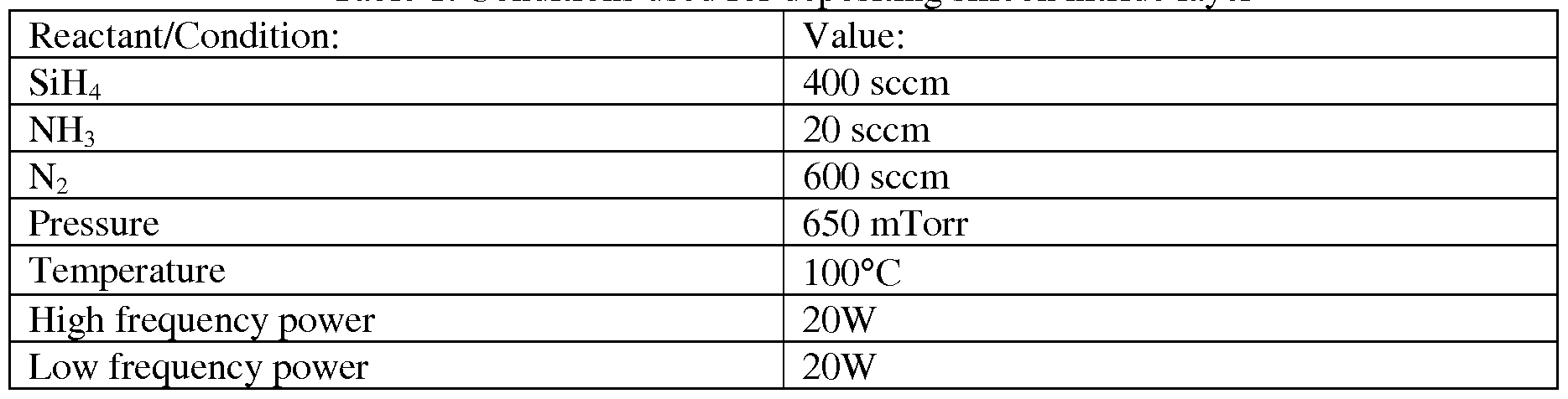
The 200nm silica-nanoparticle -coated ID pattern with backfill was then over-coated with a 100 nm thick layer of silicon nitride by plasma-enhanced chemical vapor deposition (PECVD, Model PLASMALAB SystemlOO available from Oxford Instruments, Yatton, UK). The parameters used in the PECVD process are described in Table 1 below:
Table 1. Conditions used for de ositin silicon nitride la er
Figure imgf000011_0001
The refractive index of the silicon nitride layer was measured using a Metricon Model 2010 Prism Coupler (Metricon Corporation, Pennington, NJ), and was found to be 1.78.
OLED fabrication on the above substrate began with approximately 1 lOnm-thick ITO deposited onto the backfill-coated nanoparticle/lD structured film through a 5mm x 5mm pixilated shadow mask to define the anode geometry. Subsequently, a simple green organic emitting layer and cathode were deposited to complete the OLED. The OLEDs were fabricated by standard thermal deposition in a vacuum system at base pressure of about 10"6 Torr. The following OLED construction was deposited: HIL (300nm) / HTL (40nm) / Green EML (30nm) / ETL (20nm) / LiF (lnm) / Al (200nm). After completion, the OLED was encapsulated with an encapsulation barrier film employing SAES getter as a desiccant and oxygen scavenger in between the encapsulation film and the OLED cathode.
For comparison, an OLED was also constructed using ID structured film without nanoparticles. Conoscope measurements showed that samples made with the ID structured film produced small regions with relatively high intensity and somewhat larger regions with lower intensity surrounded by regions of relatively low intensity. In contrast, the conoscope data for samples made with 200nm nanoparticles coated on ID structured film showed a much more uniform intensity distribution. This data demonstrated that the 200nm nanoparticles coated on ID structured film significantly improved angular uniformity of the OLED device compared to ID structured film without nanoparticles. Examples 2A and 2B: 440nm Si02 Nanoparticles on ID and 2D Structured Film
Solution B (440nm Si02 nanoparticles) was coated onto film having 600nm ID structures (Example 2A) and onto film having 500nm 2D structures (Example 2B) using #5 wire -wound rods (obtained from RD Specialties, Webster, NY). The resulting films were dried in air for 10 min and then UV cured as described in Example 1A. HI-BF solution was coated on the nanoparticle coated ID and 2D structured films using a #10 wire-wound rod (obtained from RD Specialties, Webster, NY). The resulting films were dried in air for 10 min and then UV cured as described in Example 1A. For comparison, coating Solution B was similarly coated onto unstructured PET film. FIGS. 9A and 9B show a top-view and a cross-sectional view of 440nm Si02 nanoparticles on ID structured film. FIG. 10 shows 440nm Si02 nanoparticles on 2D structured film. These figures show that the nanoparticles are partially ordered in these examples. In contrast, the distribution of nanoparticles is typically random when nanoparticles are coated onto a flat surface. lOOnm silicon nitride, lOOnm ITO, and OLED layers were deposited onto ID structured film (comparative), onto 2D structured film (comparative), onto a glass substrate (comparative), onto 440nm nanoparticles on ID structured film (Example 2A), and onto 440nm nanoparticles on 2D structured film (Example 2B) as described in Example 1A.
Conoscope measurements were made for the OLED device with nanoparticles on ID structured film as well as the comparative samples. The glass control sample showed a relatively uniform but relatively low intensity distribution. The ID structured film sample produced small regions with relatively high intensity and somewhat larger regions with lower intensity surrounded by regions of relatively low intensity. Samples made from 440nm nanoparticles on ID structured film showed a uniform and high intensity distribution. Samples made from 440nm nanoparticles on unstructured film gave a relatively low intensity region near the center of the conoscope plot surrounded by relatively high intensity regions. The conoscope results showed that the self-assembled 440nm nanoparticles on ID structured film significantly improved angular uniformity of the OLED device compared to either ID structured film with no nanoparticles or compared to 440nm nanoparticles coated onto unstructured film. The integrated gain was found to be significantly higher for Example 2A than for the comparative samples.
Similarly, conoscope data was obtained for the OLED devices built onto the 440nm nanoparticle coated 2D structured film (Example 2B) and for comparison for the OLED devices built onto 2D structured film without nanoparticles. The conoscope data for samples made using the 2D structured film without nanoparticles showed a band of relatively high intensity surrounded by lower intensity regions. For the samples with 2D structured film with 440nm nanoparticles, the intensity was much more uniform, but the relatively high intensity region of the 2D pattern was not completely eliminated. The integrated gain was found to be significantly higher for Example 2B than for the comparative samples. The luminance determined from the conoscope data are shown in FIGS. 11 A and 1 IB. FIG. 11 A shows the luminance as a function of polar angle along a zero degree azimuth relative to axes of the 2D structures for samples with 2D structured film with and without nanoparticles, and FIG. 1 IB shows the luminance as a function of polar angle for samples made using nanoparticles on a flat film.
Example 3: 440nm Si02 Nanoparticles Mixed with Back Fill on ID Structure
Solution C (440nm Si02 nanoparticles) was coated onto 600nm ID structured film using #5 and #10 wire -wound rods (obtained from RD Specialties, Webster, NY). The resulting films were then dried in air for 10 min and then UV cured as described in Example 1A. The refractive index of the layer of 440nm nanoparticles mixed with backfill was measured using a Metricon Model 2010 Prism Coupler, and was found to be 1.83.
lOOnm silicon nitride and OLED layers were deposited onto a glass control (comparative), onto a ID structured film without nanoparticles (comparative), and onto the ID structured film with 440nm nanoparticles in backfill (Example 3) as in Example 1A. Conoscope data was obtained for OLED device of Example 3 as well as the comparative samples. The 440nm nanoparticles in backfill on ID structured film significantly improved both angular uniformity of the OLED device and integrated gain. FIG. 12 shows the luminance as a function of polar angle along a zero degree azimuth relative to direction of the ID structures for samples with ID structured film with and without nanoparticles and for the sample made using the glass substrate without nanoparticles or nanostructures.
Examples 4 and 5: Roll to Roll Process for Hybrid Light Extraction Film
Two Step Process (Example 4)
Solution B (440nm Si02 nanoparticles) was coated onto film having 600nm ID structures using a roll to roll coating process with a web speed of 3.0 m/min (10 ft/min) and a dispersion delivery rate of 4.7 cc/min. The coating was dried in air at room temperature, then subsequently further dried at 82 °C (180 °F) and then cured using a Fusion UV-Systems Inc. Light-Hammer 6 UV (Gaithersburg, Maryland) processor equipped with an H-bulb, operating under nitrogen atmosphere at 75% lamp power at a line speed of 3.0 m/min (10 ft/min). An SEM photo of the resulting nanoparticle coating is shown in FIG. 13 where it can be seen that the 440 nm Si02 nanoparticles were partially ordered by the 600nm ID structures. HI-BF solution was coated onto the nanoparticle coated ID structured film using a roll to roll coating process with a web speed of 3.0 m/min (10 ft/min) and a dispersion delivery rate of 2.28 cc/min. The coating was dried in air at room temperature, then subsequently further dried at 82 °C (180 °F) and then cured using a Fusion UV-Systems Inc. Light-Hammer 6 UV
(Gaithersburg, Maryland) processor equipped with an H-bulb, operating under nitrogen atmosphere at 75% lamp power at a line speed of 3.0 m min (10 ft/min).
One Step Process (Example 5)
Solution C (440nm Si02 nanoparticles) was coated onto film having 600nm ID structures using a roll to roll coating process with a web speed of 4.6 m/min (15 ft/min) and a dispersion delivery rate of 7.29 cc/min. The coating was dried in air at room temperature, then subsequently further dried at 82 °C (180 °F) and then cured using a Fusion UV-Systems Inc. Light-Hammer 6 UV (Gaithersburg, Maryland) processor equipped with an H-bulb, operating under nitrogen atmosphere at 75% lamp power at a line speed of 4.6 m/min (15 ft/min). An SEM image of the resulting 440nm NP mixed in backfill on 600nm ID structured film showed that backfill effectively planarized the ID structure. For comparison, coating Solution C was similarly coated onto unstructured PET film.
OLED Devices and Conoscope Results
lOOnm silicon nitride, lOOnm ITO, and OLED layers were deposited onto 440nm nanoparticles on ID structured film (Example 4), onto 440nm nanoparticles in backfill on ID structured film (Example 5), onto 440nm nanoparticles in backfill on unstructured PET film (comparative) and onto a glass substrate (comparative). Green emitting OLEDs were made as described in Example 1A. Red OLEDs were constructed similarly but with the following OLED layers: HIL (300nm) / HTL (40nm) / Red EML (30nm) / ETL (20nm) / LiF (lnm) / Al (200nm).
Conoscope measurements were made for multiple samples. The conoscope results showed that the self-assembled 440nm nanoparticles on ID structured film (Example 4) significantly improved angular uniformity of the OLED device compared to either ID structured film with no nanoparticles or to 440nm nanoparticles coated onto unstructured film. Table 2 shows a summary of on-axis gain and total (integrated) gain for green and red OLEDs for
Examples 4 and 5 and for OLEDs made using nanoparticles on unstructured film (comparative). The gains reported in Table 2 are normalized so that the samples made using a glass substrate with no extraction features had an integrated gain of unity. Table 2.
Figure imgf000015_0001

Claims

1. A light extraction film having nanoparticles and periodic structures, comprising:
a substantially transparent substrate;
periodic structures on the substantially transparent substrate;
light scattering nanoparticles applied in a surface layer manner over the periodic structures; and
a planarizing backfill layer applied over the periodic structures and the nanoparticles, forming a substantially planar surface of the backfill layer,
wherein an index of refraction of the backfill layer is higher than an index of refraction of the periodic structures.
2. The light extraction film of claim 1 , wherein the periodic structures are one-dimensional.
3. The light extraction film of claim 2, wherein the periodic structures comprise linear prisms.
4. The light extraction film of claim 1 , wherein the periodic structures are two-dimensional.
5. The light extraction film of claim 4, wherein the periodic structures comprise pyramids.
6. The light extraction film of claim 1, wherein the periodic structures comprise photonic crystal structures or linear gratings.
7. The light extraction film of claim 1, wherein the nanoparticles are at least partially ordered by the periodic structures.
8. The light extraction film of claim 1, wherein the nanoparticles have diameters in the range of lOOnm to Ι,ΟΟΟηιη.
9. The light extraction film of claim 1, wherein the periodic structures are formed integrally with the substrate.
10. The light extraction film of claim 1, further comprising an adhesive optical coupling layer applied to the substantially planar surface of the backfill layer.
11. The light extraction film of claim 1 , where the planarizing backfill layer comprises an adhesive for bonding the light extraction film to a light output surface of an OLED device.
12. The light extraction film of claim 1, wherein the light scattering nanoparticles are aligned by the periodic structures.
13. A light extraction film having nanoparticles and periodic structures, comprising:
a substantially transparent substrate;
periodic structures on the substantially transparent substrate;
a planarizing backfill layer applied over the periodic structures, forming a substantially planar surface of the backfill layer; and
light scattering nanoparticles distributed throughout the backfill layer,
wherein an index of refraction of the backfill layer is higher than an index of refraction of the periodic structures.
14. The light extraction film of claim 13, wherein the periodic structures are one-dimensional.
15. The light extraction film of claim 14, wherein the periodic structures comprise linear prisms.
16. The light extraction film of claim 13, wherein the periodic structures are two-dimensional.
17. The light extraction film of claim 16, wherein the periodic structures comprise pyramids.
18. The light extraction film of claim 13, wherein the periodic structures comprise photonic crystal structures or linear gratings.
19. The light extraction film of claim 13, wherein the nanoparticles have diameters in the range of lOOnm to Ι,ΟΟΟηιη.
20. The light extraction film of claim 13, wherein the nanoparticles have diameters in the range of lOnm to 300nm, and form agglomerations with sizes in the range of lOOnm to Ι,ΟΟΟηιη.
21. The light extraction film of claim 13, wherein the periodic structures are formed integrally with the substrate.
22. The light extraction film of claim 13, further comprising an adhesive optical coupling layer applied to the substantially planar surface of the backfill layer.
23. The light extraction film of claim 13, where the planarizing backfill layer comprises an adhesive for bonding the film to a light output surface of an OLED device.
24. A method for providing a light extraction film on an organic light emitting diode (OLED) device having a surface that outputs light, comprising:
providing a light extraction film, comprising:
a substantially transparent substrate;
periodic structures on the substantially transparent substrate;
light scattering nanoparticles applied in a surface layer manner over the periodic structures; and
a planarizing backfill layer applied over the periodic structures and the nanoparticles, forming a substantially planar surface of the backfill layer,
wherein an index of refraction of the backfill layer is higher than an index of refraction of the periodic structures;
applying an adhesive to the substantially planar surface of the backfill layer; and laminating the light extraction film to the OLED device such that the substantially planar surface of the backfill layer is located against the light output surface of the OLED device, wherein the adhesive provides for optical coupling between the light output surface of the OLED device and the backfill layer.
25. A method for providing a light extraction film on an organic light emitting diode (OLED) device having a surface that outputs light, comprising:
providing a light extraction film, comprising:
a substantially transparent substrate;
periodic structures on the substantially transparent substrate; light scattering nanoparticles applied in a surface layer manner over the periodic structures; and
a planarizing backfill layer applied over the periodic structures and the nanoparticles, forming a substantially planar surface of the backfill layer,
wherein an index of refraction of the backfill layer is higher than an index of refraction of the periodic structures;
applying an adhesive to the light output surface of the OLED device; and
laminating the light extraction film to the OLED device such that the substantially planar surface of the backfill layer is located against the light output surface of the OLED device, wherein the adhesive provides for optical coupling between the light output surface of the OLED device and the backfill layer.
26. A method for providing a light extraction film on an organic light emitting diode (OLED) device having a surface that outputs light, comprising:
providing a light extraction film, comprising:
a substantially transparent substrate;
periodic structures on the substantially transparent substrate;
a planarizing backfill layer applied over the periodic structures, forming a substantially planar surface of the backfill layer; and
light scattering nanoparticles distributed throughout the backfill layer, wherein an index of refraction of the backfill layer is higher than an index of refraction of the periodic structures;
applying an adhesive to the substantially planar surface of the backfill layer; and laminating the light extraction film to the OLED device such that the substantially planar surface of the backfill layer is located against the light output surface of the OLED device, wherein the adhesive provides for optical coupling between the light output surface of the OLED device and the backfill layer.
27. A method for providing a light extraction film on an organic light emitting diode (OLED) device having a surface that outputs light, comprising:
providing a light extraction film, comprising:
a substantially transparent substrate;
periodic structures on the substantially transparent substrate; a planarizing backfill layer applied over the periodic structures, forming a substantially planar surface of the backfill layer; and
light scattering nanoparticles distributed throughout the backfill layer, wherein an index of refraction of the backfill layer is higher than an index of refraction of the periodic structures;
applying an adhesive to the light output surface of the OLED device; and
laminating the light extraction film to the OLED device such that the substantially planar surface of the backfill layer is located against the light output surface of the OLED device, wherein the adhesive provides for optical coupling between the light output surface of the OLED device and the backfill layer.
PCT/US2012/027681 2011-03-17 2012-03-05 Oled light extraction films having nanoparticles and periodic structures WO2012125321A2 (en)

Priority Applications (4)

Application Number Priority Date Filing Date Title
KR1020137026986A KR101932298B1 (en) 2011-03-17 2012-03-05 Oled light extraction films having nanoparticles and periodic structures
EP12758354.0A EP2686896A4 (en) 2011-03-17 2012-03-05 Oled light extraction films having nanoparticles and periodic structures
CN201280013109.8A CN103443952B (en) 2011-03-17 2012-03-05 The oled light with nano particle and periodic structure extracts film
JP2013558040A JP6169982B2 (en) 2011-03-17 2012-03-05 OLED light extraction film having nanoparticles and periodic structure

Applications Claiming Priority (2)

Application Number Priority Date Filing Date Title
US13/050,324 US8692446B2 (en) 2011-03-17 2011-03-17 OLED light extraction films having nanoparticles and periodic structures
US13/050,324 2011-03-17

Publications (2)

Publication Number Publication Date
WO2012125321A2 true WO2012125321A2 (en) 2012-09-20
WO2012125321A3 WO2012125321A3 (en) 2012-11-22

Family

ID=46827508

Family Applications (1)

Application Number Title Priority Date Filing Date
PCT/US2012/027681 WO2012125321A2 (en) 2011-03-17 2012-03-05 Oled light extraction films having nanoparticles and periodic structures

Country Status (7)

Country Link
US (1) US8692446B2 (en)
EP (1) EP2686896A4 (en)
JP (1) JP6169982B2 (en)
KR (1) KR101932298B1 (en)
CN (1) CN103443952B (en)
TW (1) TWI575796B (en)
WO (1) WO2012125321A2 (en)

Cited By (7)

* Cited by examiner, † Cited by third party
Publication number Priority date Publication date Assignee Title
CN103367655A (en) * 2013-07-17 2013-10-23 五邑大学 High luminance OLED based on photonic crystal microstructure substrate and manufacturing method thereof
WO2016033189A3 (en) * 2014-08-27 2016-05-06 3M Innovative Properties Company Thermally-assisted self-assembly method of nanoparticles and nanowires within engineered periodic structures
JPWO2015012093A1 (en) * 2013-07-26 2017-03-02 コニカミノルタ株式会社 Manufacturing method of organic electroluminescence device and coating solution
JPWO2015147294A1 (en) * 2014-03-28 2017-04-13 日産化学工業株式会社 Surface roughening method
US9634290B2 (en) 2013-10-08 2017-04-25 Saint-Gobain Glass France Laminate for light emitting device and process of preparing same
US10243171B2 (en) 2013-07-17 2019-03-26 Saint-Gobain Glass France Laminate for light emitting device and process of preparing same
US11396156B2 (en) 2012-12-21 2022-07-26 3M Innovative Properties Company Patterned structured transfer tape

Families Citing this family (40)

* Cited by examiner, † Cited by third party
Publication number Priority date Publication date Assignee Title
US8659221B2 (en) 2011-08-26 2014-02-25 3M Innovative Properties Company OLED light extraction film with multi-periodic zones of nanostructures
WO2013065213A1 (en) * 2011-11-02 2013-05-10 パナソニック株式会社 Organic light-emitting panel and method for producing same
US9818983B2 (en) 2012-02-28 2017-11-14 3M Innovative Properties Composition comprising surface modified high index nanoparticles suitable for optical coupling layer
JP6290888B2 (en) 2012-08-22 2018-03-07 スリーエム イノベイティブ プロパティズ カンパニー Transparent OLED light extractor
KR20150091111A (en) 2012-11-30 2015-08-07 쓰리엠 이노베이티브 프로퍼티즈 컴파니 Emissive display with reflective polarizer
EP2926334A4 (en) 2012-11-30 2016-08-10 3M Innovative Properties Co Emissive display with hybrid polarizer
US9335027B2 (en) * 2013-01-02 2016-05-10 Massachusetts Institute Of Technology Methods and apparatus for transparent display using scattering nanoparticles
WO2014107425A1 (en) * 2013-01-02 2014-07-10 Massachusetts Institute Of Technology Methods and apparatus for transparent display using scattering nanoparticles
US9366787B2 (en) * 2013-03-12 2016-06-14 Ppg Industries Ohio, Inc. Organic light emitting diode with light extracting layer
KR101466831B1 (en) * 2013-07-03 2014-11-28 코닝정밀소재 주식회사 Light extraction substrate for oled, method of fabricating thereof and oled including the same
KR20150012520A (en) 2013-07-25 2015-02-04 삼성디스플레이 주식회사 Organic light emitting display and manufacturing method thereof
JP2016527571A (en) 2013-08-12 2016-09-08 スリーエム イノベイティブ プロパティズ カンパニー Luminescent article having light extraction film
CN103531720A (en) * 2013-10-29 2014-01-22 南京第壹有机光电有限公司 Electroluminescent device with high light emitting efficiency
WO2015069444A1 (en) * 2013-11-11 2015-05-14 3M Innovative Properties Company Nanostructures for oled devices
EP2897186B1 (en) * 2014-01-21 2018-12-26 Covestro Deutschland AG UV protection film for OLEDs
TW201539736A (en) * 2014-03-19 2015-10-16 3M Innovative Properties Co Nanostructures for color-by-white OLED devices
DE102014107099B4 (en) 2014-05-20 2019-10-31 Fraunhofer-Gesellschaft zur Förderung der angewandten Forschung e.V. Light-scattering layer system, method for its production and use of the layer system
US9570712B2 (en) 2014-07-31 2017-02-14 Industrial Technology Research Institute Organic light-emitting module
GB2523859B (en) * 2014-08-01 2016-10-19 Dupont Teijin Films U S Ltd Partnership Polyester film assembly
JP6553735B2 (en) 2015-03-13 2019-07-31 ダウ グローバル テクノロジーズ エルエルシー Method and device for nanostructured material
CA2889103A1 (en) * 2015-04-21 2016-10-21 Claudine Allen Hybrid nanocomposite materials and their application in a volumetric projection system
CN105226198A (en) 2015-10-13 2016-01-06 京东方科技集团股份有限公司 A kind of waterproof transmission increasing flexible OLED devices device and preparation method thereof
CN105355798A (en) * 2015-11-25 2016-02-24 京东方科技集团股份有限公司 Organic electroluminescent device, manufacturing method thereof, and display device
EP3188260B1 (en) 2015-12-31 2020-02-12 Dow Global Technologies Llc Nanostructure material structures and methods
CN105589125A (en) * 2016-03-11 2016-05-18 深圳市华星光电技术有限公司 Light guide plate, backlight module and double-surface display device
WO2017173289A2 (en) 2016-04-01 2017-10-05 Massachusetts Institute Of Technology Apparatus, systems, and methods of transparent displays
KR20190026776A (en) 2016-07-12 2019-03-13 코닝 인코포레이티드 Waveguide including a light extracting nanostructure and a display element including the same
US20180097202A1 (en) * 2016-10-03 2018-04-05 Regents Of The University Of Michigan Enhanced oled outcoupling by suppressing surface plasmon modes
CN106684256A (en) * 2016-12-23 2017-05-17 上海天马有机发光显示技术有限公司 Display panel and fabrication method thereof
CN106654064B (en) * 2016-12-29 2019-02-12 深圳市华星光电技术有限公司 A kind of preparation method and applications of top emission OLED device refraction passivation layer
US10121919B2 (en) 2017-01-06 2018-11-06 Nanoclear Technologies Inc. Control of surface properties by deposition of particle monolayers
US10017384B1 (en) 2017-01-06 2018-07-10 Nanoclear Technologies Inc. Property control of multifunctional surfaces
CN106935725A (en) * 2017-02-17 2017-07-07 武汉华星光电技术有限公司 Organic electroluminescence display device and method of manufacturing same
JP7285219B2 (en) 2017-05-05 2023-06-01 スリーエム イノベイティブ プロパティズ カンパニー Display device containing polymer film
CN107195799B (en) * 2017-07-26 2019-05-10 上海天马有机发光显示技术有限公司 Organic light emitting display panel and display device
EP3788420A1 (en) 2018-04-30 2021-03-10 Corning Incorporated Small outer diameter low attenuation optical fiber
CN113614940A (en) 2018-06-06 2021-11-05 康宁公司 Light extraction device and OLED display
WO2020123451A1 (en) * 2018-12-10 2020-06-18 Nanoclear Technologies, Inc. Enhancement of photon extraction with nanoparticles on semiconducting nanostructures
WO2021231083A1 (en) 2020-05-12 2021-11-18 Corning Incorporated Reduced diameter single mode optical fibers with high mechanical reliability
CN111487711A (en) * 2020-05-29 2020-08-04 北京小米移动软件有限公司 Optical component, backlight module, electronic equipment and manufacturing method of optical component

Citations (1)

* Cited by examiner, † Cited by third party
Publication number Priority date Publication date Assignee Title
US20050007000A1 (en) 2000-11-02 2005-01-13 3M Innovative Properties Company Brightness and contrast enhancement of direct view emissive displays

Family Cites Families (39)

* Cited by examiner, † Cited by third party
Publication number Priority date Publication date Assignee Title
US6015719A (en) 1997-10-24 2000-01-18 Hewlett-Packard Company Transparent substrate light emitting diodes with directed light output
WO2002033461A2 (en) 2000-10-16 2002-04-25 Ozin Geoffrey A Method of self-assembly and optical applications of crystalline colloidal patterns on substrates
JP2003115377A (en) * 2001-10-03 2003-04-18 Nec Corp Light emitting element, its manufacturing method, and display equipment using this
US20030152703A1 (en) 2001-10-31 2003-08-14 Hammond Paula T. Production of chemically patterned surfaces using polymer-on-polymer stamping
KR100581850B1 (en) 2002-02-27 2006-05-22 삼성에스디아이 주식회사 Organic electro luminescence display device and method of manufacturing the same
US7140812B2 (en) 2002-05-29 2006-11-28 3M Innovative Properties Company Diamond tool with a multi-tipped diamond
JP2004055461A (en) 2002-07-23 2004-02-19 Seiko Epson Corp Light emitting device and its manufacturing method as well as electronic equipment
KR100875097B1 (en) 2002-09-18 2008-12-19 삼성모바일디스플레이주식회사 Organic electroluminescent device using optical resonance effect
JP3703028B2 (en) 2002-10-04 2005-10-05 ソニー株式会社 Display element and display device using the same
JP4822243B2 (en) 2003-03-25 2011-11-24 国立大学法人京都大学 LIGHT EMITTING ELEMENT AND ORGANIC ELECTROLUMINESCENT LIGHT EMITTING ELEMENT
KR100563059B1 (en) 2003-11-28 2006-03-24 삼성에스디아이 주식회사 Electroluminescence display device and laser induced thermal imaging donor film for the electroluminescence display device
US7247394B2 (en) 2004-05-04 2007-07-24 Eastman Kodak Company Tuned microcavity color OLED display
CN100457443C (en) * 2004-05-26 2009-02-04 日产化学工业株式会社 Planar luminous body
WO2006030949A1 (en) 2004-09-16 2006-03-23 Fujifilm Corporation Method of producing light-scattering film, polarizing plate comprising light-scattering film and liquid crystal display device comprising the polarizing plate
US20060063015A1 (en) 2004-09-23 2006-03-23 3M Innovative Properties Company Protected polymeric film
KR100715500B1 (en) * 2004-11-30 2007-05-07 (주)케이디티 Light source with micro-cavity organic light emitting diode and photoluminescent layer
KR20060061017A (en) 2004-12-01 2006-06-07 두산중공업 주식회사 Method of generating and managing piping drawings in the plant
JP4253302B2 (en) 2005-01-06 2009-04-08 株式会社東芝 Organic electroluminescence device and method for producing the same
US20070020451A1 (en) 2005-07-20 2007-01-25 3M Innovative Properties Company Moisture barrier coatings
US20070201056A1 (en) * 2006-02-24 2007-08-30 Eastman Kodak Company Light-scattering color-conversion material layer
JP2007335253A (en) 2006-06-15 2007-12-27 Toshiba Matsushita Display Technology Co Ltd Organic el display device
JP2008003525A (en) * 2006-06-26 2008-01-10 Fujifilm Corp Optically functional sheet and method of manufacturing the same
CN101122703B (en) * 2006-08-11 2010-12-01 鸿富锦精密工业(深圳)有限公司 Optical board and the backlight module using same
US20080088933A1 (en) * 2006-10-16 2008-04-17 Ching-Bin Lin Optical film for overcoming optical defects
KR101321909B1 (en) * 2006-12-12 2013-10-25 삼성디스플레이 주식회사 Prism sheet and manufacturing method thereof
WO2008100057A1 (en) * 2007-02-13 2008-08-21 Kolon Industries, Inc. Cover sheet for prism and backlight unit assembly
US8179034B2 (en) 2007-07-13 2012-05-15 3M Innovative Properties Company Light extraction film for organic light emitting diode display and lighting devices
US20090015142A1 (en) 2007-07-13 2009-01-15 3M Innovative Properties Company Light extraction film for organic light emitting diode display devices
US20090279175A1 (en) 2008-05-07 2009-11-12 Rohm And Haas Denmark Finance A/S Optical diffuser film with linear domains of varying diffusion
EP2308102A4 (en) * 2008-06-26 2014-05-07 3M Innovative Properties Co Method of fabricating light extractor
JP5028366B2 (en) * 2008-09-11 2012-09-19 株式会社ジャパンディスプレイイースト Organic light emitting device
US20100110551A1 (en) 2008-10-31 2010-05-06 3M Innovative Properties Company Light extraction film with high index backfill layer and passivation layer
US20100128351A1 (en) 2008-11-21 2010-05-27 3M Innovative Properties Company Curved sided cone structures for controlling gain and viewing angle in an optical film
US7957621B2 (en) 2008-12-17 2011-06-07 3M Innovative Properties Company Light extraction film with nanoparticle coatings
KR101679895B1 (en) 2009-04-15 2016-11-25 쓰리엠 이노베이티브 프로퍼티즈 컴파니 Process and apparatus for a nanovoided article
US10539722B2 (en) 2009-04-15 2020-01-21 3M Innovative Properties Company Optical film
CN102712140B (en) 2010-01-13 2015-06-03 3M创新有限公司 Optical films with microstructured low refractive index nanovoided layers and methods therefor
US8538224B2 (en) 2010-04-22 2013-09-17 3M Innovative Properties Company OLED light extraction films having internal nanostructures and external microstructures
CN102540294B (en) * 2012-02-03 2016-01-13 北京康得新复合材料股份有限公司 A kind of bright enhancement film

Patent Citations (1)

* Cited by examiner, † Cited by third party
Publication number Priority date Publication date Assignee Title
US20050007000A1 (en) 2000-11-02 2005-01-13 3M Innovative Properties Company Brightness and contrast enhancement of direct view emissive displays

Cited By (10)

* Cited by examiner, † Cited by third party
Publication number Priority date Publication date Assignee Title
US11396156B2 (en) 2012-12-21 2022-07-26 3M Innovative Properties Company Patterned structured transfer tape
US11565495B2 (en) 2012-12-21 2023-01-31 3M Innovative Properties Company Patterned structured transfer tape
CN103367655A (en) * 2013-07-17 2013-10-23 五邑大学 High luminance OLED based on photonic crystal microstructure substrate and manufacturing method thereof
US10243171B2 (en) 2013-07-17 2019-03-26 Saint-Gobain Glass France Laminate for light emitting device and process of preparing same
JPWO2015012093A1 (en) * 2013-07-26 2017-03-02 コニカミノルタ株式会社 Manufacturing method of organic electroluminescence device and coating solution
US9634290B2 (en) 2013-10-08 2017-04-25 Saint-Gobain Glass France Laminate for light emitting device and process of preparing same
JPWO2015147294A1 (en) * 2014-03-28 2017-04-13 日産化学工業株式会社 Surface roughening method
WO2016033189A3 (en) * 2014-08-27 2016-05-06 3M Innovative Properties Company Thermally-assisted self-assembly method of nanoparticles and nanowires within engineered periodic structures
US9472788B2 (en) 2014-08-27 2016-10-18 3M Innovative Properties Company Thermally-assisted self-assembly method of nanoparticles and nanowires within engineered periodic structures
US9761844B2 (en) 2014-08-27 2017-09-12 3M Innovative Properties Company Lamination transfer films including oriented dimensionally anisotropic inorganic nanomaterials

Also Published As

Publication number Publication date
TW201304231A (en) 2013-01-16
EP2686896A4 (en) 2015-03-18
US20120234460A1 (en) 2012-09-20
WO2012125321A3 (en) 2012-11-22
CN103443952B (en) 2016-04-13
CN103443952A (en) 2013-12-11
KR20140023311A (en) 2014-02-26
EP2686896A2 (en) 2014-01-22
US8692446B2 (en) 2014-04-08
JP2014508329A (en) 2014-04-03
JP6169982B2 (en) 2017-07-26
KR101932298B1 (en) 2018-12-24
TWI575796B (en) 2017-03-21

Similar Documents

Publication Publication Date Title
US8692446B2 (en) OLED light extraction films having nanoparticles and periodic structures
JP5543480B2 (en) Light extraction film comprising a high refractive index filler layer and a passivation layer
TWI581476B (en) Oled light extraction film with multi-periodic zones of nanostructures
TWI689754B (en) Emissive display with reflective polarizer
TWI515111B (en) Light extraction film with nanoparticle coatings
TWI596813B (en) Light emitting device, active matrix organic light emitting diode device and image display device
KR20150046128A (en) Transparent oled light extraction
KR20160042962A (en) Emissive article with light extraction film

Legal Events

Date Code Title Description
121 Ep: the epo has been informed by wipo that ep was designated in this application

Ref document number: 12758354

Country of ref document: EP

Kind code of ref document: A2

ENP Entry into the national phase

Ref document number: 2013558040

Country of ref document: JP

Kind code of ref document: A

NENP Non-entry into the national phase

Ref country code: DE

WWE Wipo information: entry into national phase

Ref document number: 2012758354

Country of ref document: EP

ENP Entry into the national phase

Ref document number: 20137026986

Country of ref document: KR

Kind code of ref document: A