EP0125633A2 - Testing apparatus for redundant memory - Google Patents
Testing apparatus for redundant memory Download PDFInfo
- Publication number
- EP0125633A2 EP0125633A2 EP84105285A EP84105285A EP0125633A2 EP 0125633 A2 EP0125633 A2 EP 0125633A2 EP 84105285 A EP84105285 A EP 84105285A EP 84105285 A EP84105285 A EP 84105285A EP 0125633 A2 EP0125633 A2 EP 0125633A2
- Authority
- EP
- European Patent Office
- Prior art keywords
- memory
- line
- redundant
- failure
- remedy
- Prior art date
- Legal status (The legal status is an assumption and is not a legal conclusion. Google has not performed a legal analysis and makes no representation as to the accuracy of the status listed.)
- Granted
Links
Images


Classifications
-
- G—PHYSICS
- G11—INFORMATION STORAGE
- G11C—STATIC STORES
- G11C29/00—Checking stores for correct operation ; Subsequent repair; Testing stores during standby or offline operation
- G11C29/70—Masking faults in memories by using spares or by reconfiguring
- G11C29/72—Masking faults in memories by using spares or by reconfiguring with optimized replacement algorithms
Definitions
- This invention relates generally to an apparatus for testing a redundant memory. More particularly, the present invention relates to an apparatus for testing redundant memory which is equipped with a failure data memory device which is suitable for the analysis of failure data needed for determining a remedy line, during a test on a memory incorporating therein redundant word lines or bit lines for remedying defective bits.
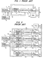
- a memory testers usually comprise a pattern generator 1 which is controlled by a timing signal output 6 from a timing generator 2, a comparator 4 which compares data output 11 from a memory 3 under test with expected-value data 10 and outputs a judgement result on the memory 3 under test, and a failure memory 5 constructed so that fail data is written into an address thereof which is the same as an address 8 given to the memory 3 under test, or corresponds thereto, when the comparison result from the comparator 12 is "failure," as illustrated in Figure 1.
- the pattern generator 1 provides the address 8 and a test pattern 9 as write data for the memory 3 under test and, at the same time, provides the expected-value data 10 for the comparator 4 and outputs a control signal 7 to the timing generator 2.
- the failure memory 5 is generally constructed of a memory which has a capacity the same as, or greater than, the capacity of the memory 3 under test, and which can be read from and written to.
- the same addresses 8 as those given to the memory 3 under test are also given to the failure memory 5 by the pattern generator 1.
- Figure 3 illustrates an example of remedying a memory in which failures 1 through 13, represented by Xs as a test results (where numerals within circles represent the sequence in which failures occurred), are remedied by two of each of lines on the column side (x) and on the row side (y) that have been prepared as redundant remedy lines.
- the example shown in Figure 3 makes it possible to remedy the failed cells 1 through 13 of the tested memory cell array 16 by two of each of redundant lines on the column and row sides, but this remedy can sometimes not be used, depending on the distribution of failure occurrences and the number of failed cells.
- the line numbers of the redundant remedy lines along the column and row sides will be hereinafter called N x and N , respectively.
- the ratio of the test cost to the memory cost is high, as is well known in the art. To reduce the test cost, therefore, attempts have been made to simultaneously test a large number of memories using a single tester. In such a case, it is possible to provide failure memories 5 1 through 5 n which store test results on memories 3 1 through 3 n under test, respectively, as the structure of the tester shown in Figure 2. Accordingly, the analysis processing for determining remedies for the data in the failure memories 5 1 through 5 n is sequentially carried out by a CPU 13 starting from the failure memory 5 1 and ending at the failure memory 5 n . For this reason, the above problem of processing time becomes even more critical.
- the memory used as the failure memory 5 must have a faster access time than that of the memory 3 under test.
- a failure memory 5 is usually composed of a combination of a-large number of memories of a smaller capacity than that of the memory 3 under test, so that the failure memory data can be easily read out using a CPU 13 or the like.
- the size of hardware required for one failure memory 5 can not be reduced very easily.
- the size and cost of the hardware for the failure memories raises a critical problem for a system in which a large number of memories are simultaneously tested.
- the present invention is directed to providing a memory tester which can conduct data analysis for such a remedy at high speed, and which can be realized compactly.
- the present invention does not use the conventional failure memories that unconditionally store all the test results of memories under test, it leaves only that data which is absolutely necessary for the remedy judgement while conducting the test, stores that data as a compressed data matrix of a small capacity, and analyzes the minimum necessary data for the remedy judgement.
- the present invention can therefore shorten the time needed for the analysis, and can reduce the scale of the necessary hardware.
- the present invention introduces the following two fundamental concepts which are used to compress test results with a high efficiency, leaving the data in a matrix form.
- Figure 5 illustrates a data compression method which eliminates data on good cells which -is unnecessary for the analysis while keeping the relative positional relationships between the failed cells within the memory under test, leaving failed cell data which is really needed for the analysis for the decision on the remedies. This method constitutes an important point of the present invention.
- addresses for a compressed data matrix 17 such as x 1 , x 21 ... , y1, y 2 ... which are different from the absolute addresses of fails, but which have a distinct correspondence to those absolute addresses, are allotted to the failures in the sequence in which they occurred, whenever failures 1 to 7 occur during the execution of the test.
- the compressed data matrix 17 holds data in a rearranged form of addresses stored in the sequence in which the failures occurred.
- the data is compressed into a small 4x4 matrix without the loss of any information on the relative positional relationships between the failures which is needed for deciding on the remedy lines, and it can be appreciated that the analysis can be done extremely easily.
- Figure 6 shows an example of a failure pattern illustrating how the size of the compressed data matrix thus obtained depends on the number of remedy lines.
- the maximum possible size of the compressed data matrix within the range in which the remedy decision described above does not occur is 6x6.
- x 1 , x 2 , y 5 and y 6 which are circled in Figure 6, can be selected as the remedy lines, from an analysis of the matrix data. This is derived from the fact that the same number of lines on which two failures are aligned can exist on the x and y sides as the number of redundant lines.
- the matrix size obtained in this manner can be expressed in terms of the number of redundant lines as follows:
- any new failures that are positioned outside the matrix stored in the sequence in which failures occurred are determined to be impossible to remedy, or remedy lines, and they can not be used as data for the analysis after the completion of the test.
- a in Figure 6 is impossible to remedy, and B shows that x 2 is determined- to be a remedy line.
- the present invention provides a matrix corresponding to the number of redundant lines of Figure 6, and has the functions of determining whether or not new failure data is within this matrix, and of deciding the remedy line determination or judging a line to be impossible to remedy if data is outside the matrix. Accordingly, the present invention leaves only that data whose analysis after the completion of the test is really necessary.
- the structure can be broadly classified into the following three sections:
- the failure line register XFLR 20 which registers the X address of a failure is a line memory (a RAM with a one-bit width and a depth the same as the X address length of the memory under test), as shown in Figure 8, inputs an output (X address) 40 from a multiplexer MUX 18 and writes the data "1" into that address. (It is assumed, of course, that initially all the memories and registers including the failure line register XFLR 20 have been cleared to "0".) If the input it receives is an address that has not already been written (to which access has not yet been made), the output of the failure line register XFLR 20 becomes "0", so that the counter 22 in the next stage is incremented by one.
- the counter counts one whenever ENB is "0". If the address is one to which "1" has already been written (to which access has already been made at least once), on the other hand, the output 42 of the failure line register XFLR 20 becomes "1", so that the counter 22 does not operate.
- the operation described above also occurs on the Y side.
- the y addresses of the compressed data matrix 17 converted and stored on the Y side are input to the decoder 35 so they can be used as-a data input D in (48) to the compressed data matrix 17.
- FIG. 10 The structure of the compressed data matrix 17 is illustrated in Figure 10.
- this embodiment employs a RAM structure with 6 inputs and a depth of 6.
- the x data (x addresses 46) is used as address inputs, while the y data (decoder outputs 48) is used as data input.
- the data obtained from the 3-bit counter 22 is input unchanged as the x addresses 46, since the address decoder is within the RAM.
- the X addresses 38 corresponding to the x addresses 44, 46 examined in advance, as described above, are input from the CPU through the multiplexer MUX 18, and the compressed data matrix output 49 is produced from D out of Figure 10.
- the CPU completes the read-out by reading 6-bit,parallel data only 6 times. It is of course possible to replace the addresses of the compressed data matrix 17 and D in by the y and x addresses, respectively, then input the Y addresses 39 to a multiplexer MUX 19 and read out the data.
- the counter provides the outputs of the double-count prevention gates 26, 27 as ENABLE signals for the RAMs 59, 60 to a chip select SC, and shifts "1" from RAM 59 to RAM 60 whenever the same address is held in the failure line registers XLFR 20, YFLR 21.
- failure line register XFLR 20 If the failure line register XFLR 20 is considered to be a first stage, RAM 59 and RAM 60 can be regarded as the second and third stages, respectively.
- the alignment of three failures on the same line means that the output from RAM 60 in the third stage at that address has become "1," and it can be understood, as shown in Figure 9, that the output can be used as such as an x remedy-decision flag 52.
- the X addresses 38 are input from the CPU through the multiplexer MUX 18, and it is possible to check their correspondence with the x addresses and, at the same time, obtain all the lines for which a remedy decision has been made from the output of the RAM 60 during the test. When the number of these lines exceeds the number of lines prepared as redundant lines, a judgement that remedy is impossible is immediately made, without the necessity of any analysis.
- the comparators 28 and 29 of Figure 7 produce outputs 54 and 55, respectively, when the number of the corresponding stored x and y addresses 44 and 45 exceeds 6.
- the example of Figure 6@ shows a pattern for which "NG" is generated in this way. In other words, there are only two failures inclusive of B on Y3 on the y side, and remedy is not decided on.
- this embodiment compresses the analysis data for the remedy judgement into a matrix of only 6x6, which is determined by the number of redundant lines, simultaneously with completion of the test, irrespective of the sized of the memory under test, and can drastically reduce the time required for reading and analyzing the data.
- this embodiment makes it possible to identify those memories being tested for which a remedy is not possible, and redundant lines can be decided on without the need of analysis, depending upon the pattern of the failure occurrences. This also results in a reduction of the analysis time.
- the embodiment makes it possible to greatly reduce the hardware construction becuase it is constituted by the compressed data matrix 17 of an extremely small capacity, and 1-bit wide memories such as the failure line registers XFLRs 20, 21, the failure counters XLFC 24, YLFC 25, the address registers XAR 33, YAR 34, etc.
- Various matrix sizes can be realized easily according to the number of redundant lines, in the same way as in this embodiment.
- Figures 11 through 14 illustrate concretely the disposition and method of construction of remedy-decision line memories, with reference to the compressed data matrix size (6x6) of Figure 6 by way of example.
- Figure 11 shows an example which is provided with two remedy-decision line memories 63, 64 for determining the remedy lines on the y side, which have an actual address length of L on the X side of the memory under test, and two remedy-decision line memories 65, 66 for determining the remedy lines on the x side which have an actual address length of Ly on the.Y side of the memory being tested.
- Figure 12 illustrates an example in which two line memories 63, 64 are provided as exclusive remedy-decision line memories on only the y side, while the memory used for the compressed data matrix is provided on the x side so that it can function as an elongated memory 17' of an actual address length of L y on the Y side of the memory under test and a 6-bit width, as shown in the drawing, and which also functions as a remedy-decision line memory.
- Figure 13 shows an example in which the x side of Figure 12 is replaced by the y side, and which is provided with line memories 65, 66 and a memory 17".
- Figure 14 shows an example in which memories on both x and y sides also function as the compressed data matrix.
- X, Y line failure counters XLFC 24 and YLFC 25 of Figure 7 can be replaced by ordinary shift registers or counters.
- defects can be remedied by using only the output of the failure line register XFLR 20 or YFLR 21 of Figure 7, and hence the present invention can be applied to both of these systems.
- the present invention tests memories of a redundant line-defect remedy system, and can compress data thereon into a data matrix of a small capacity leaving only failure data for which a remedy judgement analysis is necessary, on the basis of test results. Accordingly, the present invention can drastically reduce analysis time as well as hardware size.
Abstract
Description
- This invention relates generally to an apparatus for testing a redundant memory. More particularly, the present invention relates to an apparatus for testing redundant memory which is equipped with a failure data memory device which is suitable for the analysis of failure data needed for determining a remedy line, during a test on a memory incorporating therein redundant word lines or bit lines for remedying defective bits.
- Heretofore known memory-testing apparatuses (hereinafter referred to as a "memory testers") usually comprise a
pattern generator 1 which is controlled by atiming signal output 6 from atiming generator 2, acomparator 4 which comparesdata output 11 from amemory 3 under test with expected-value data 10 and outputs a judgement result on thememory 3 under test, and afailure memory 5 constructed so that fail data is written into an address thereof which is the same as anaddress 8 given to thememory 3 under test, or corresponds thereto, when the comparison result from thecomparator 12 is "failure," as illustrated in Figure 1. - The
pattern generator 1 provides theaddress 8 and atest pattern 9 as write data for thememory 3 under test and, at the same time, provides the expected-value data 10 for thecomparator 4 and outputs a control signal 7 to thetiming generator 2. - The
failure memory 5 is generally constructed of a memory which has a capacity the same as, or greater than, the capacity of thememory 3 under test, and which can be read from and written to. Thesame addresses 8 as those given to thememory 3 under test are also given to thefailure memory 5 by thepattern generator 1. - However, as memory_capacities have become larger, a recent technical trend has been directed to improving the production process in order to improve the production yield that has dropped with the increase in memory capacity. An attempt has also been made to improving the yield by improving the memory device itself. In other words, a method is now employed in which any defective bits in the memory are remedied by replacing them in line units by redundant bit lines or word lines incorporated in the memory.
- Figure 3 illustrates an example of remedying a memory in which
failures 1 through 13, represented by Xs as a test results (where numerals within circles represent the sequence in which failures occurred), are remedied by two of each of lines on the column side (x) and on the row side (y) that have been prepared as redundant remedy lines. - The example shown in Figure 3 makes it possible to remedy the failed
cells 1 through 13 of the testedmemory cell array 16 by two of each of redundant lines on the column and row sides, but this remedy can sometimes not be used, depending on the distribution of failure occurrences and the number of failed cells. The line numbers of the redundant remedy lines along the column and row sides will be hereinafter called N x and N , respectively. - Data analysis for judging whether or not a remedy is possible from the distribution and number of failure data, and for determining the remedy lines, is conventionally carried out using the data within the
failure memory 5 of Figure 1, after the test is completed. However, this remedy processing should not be considered simply as the collection of data on test results, but should rather be regarded as a part of the production process for completing the memory. Accordingly, processing on an on-line, real-time basis within a short period of time is required. - This means that the conventional method described above, merely using a failure memory whose capacity is the same as, or greater than, that of the memory under test which is prepared for the data analysis, is not sufficient because a considerable length of time is needed just for searching the content of the memory to determine the failure addresses. Thus the method can not easily satisfy the requirements for memories with a large capacity.
- Moreover, the ratio of the test cost to the memory cost is high, as is well known in the art. To reduce the test cost, therefore, attempts have been made to simultaneously test a large number of memories using a single tester. In such a case, it is possible to provide
failure memories 51 through 5n which store test results onmemories 31 through 3n under test, respectively, as the structure of the tester shown in Figure 2. Accordingly, the analysis processing for determining remedies for the data in thefailure memories 51 through 5n is sequentially carried out by aCPU 13 starting from thefailure memory 51 and ending at thefailure memory 5n. For this reason, the above problem of processing time becomes even more critical. - From the point of view of hardware size and construction, the memory used as the
failure memory 5 must have a faster access time than that of thememory 3 under test. However, afailure memory 5 is usually composed of a combination of a-large number of memories of a smaller capacity than that of thememory 3 under test, so that the failure memory data can be easily read out using aCPU 13 or the like. When the construction of peripheral circuits required for controlling the read and write for onefailure memory 5 is taken into consideration, therefore, the size of hardware required for onefailure memory 5 can not be reduced very easily. Thus, the size and cost of the hardware for the failure memories raises a critical problem for a system in which a large number of memories are simultaneously tested. - In a memory tester which can eliminate the problems in the prior-art technique, and which tests a memory in such a way that it can remedy failed bits by using redundant lines incorporated in the memory, the present invention is directed to providing a memory tester which can conduct data analysis for such a remedy at high speed, and which can be realized compactly.
- The present invention does not use the conventional failure memories that unconditionally store all the test results of memories under test, it leaves only that data which is absolutely necessary for the remedy judgement while conducting the test, stores that data as a compressed data matrix of a small capacity, and analyzes the minimum necessary data for the remedy judgement. The present invention can therefore shorten the time needed for the analysis, and can reduce the scale of the necessary hardware.
-
- Figure 1 is a block diagram of an ordinary semiconductor memory tester;
- Figure 2 is a block diagram of an ordinary tester which simultaneously tests a plurality of memories;
- Figure 3 is a diagram illustrating how failed bits are remedied by redundant lines;
- Figures 4(a), 4(b) and 4(c) are schematic views illustrating the principle of determining remedy lines;
- Figure 5 is a schematic view illustrating a method of compressing the failure data on a memory under test, in which (a) shows a tested memory cell array, and (b) shows a compressed data matrix;
- Figure 6 is a diagram of an analysis method for determining remedy lines, using the compressed data matrix;
- Figure 7 is a block diagram of the construction of one embodiment of the present invention;
- Figure 8 is a block diagram of the construction of a failure line register of the embodiment of the present invention;
- Figure 9 is a block diagram of the construction of a line-failure counter;
- Figure 10 is a block diagram of the construction of the compressed data matrix; and
- Figures 11 through 14 are block diagrams of examples of the construction of compressed data matrices equipped with remedy-decision line memories.
- The present invention introduces the following two fundamental concepts which are used to compress test results with a high efficiency, leaving the data in a matrix form.
- (1) The possibility of remedy using the redundant lines incorporated in the memory under test (such as that indicated by
reference numeral 3 in Figure 1) is judged while the test is being conducted, whenever the comparator (indicated by reference numeral 4) outputs a failure result, and no remedy processing is carried out for any memory for which remedy is judged to be impossible on the basis of the failure pattern and number of failures generated up to that time. In other words, that memory is judged to be "NG" (no good;,-and subsequent failure results are not input for it. On the other hand, the testing is continued to the end for those of the memories for which an analysis of the remedy judgement indicate the possibility of remedy, even if failure data has been input for them. After the test is completed, judgement processing of the remedy lines is conducted on the failure data remaining in compressed matrix form, to provide an analysis for remedy judgement. - (2) It is possible to decide on remedy lines during the test in the same way as in the judgement of remedy impossibility described in (1) above. Accordingly, exclusive line memories used for storing the failure data, which is subsequently input for the lines thus decided on, are prepared for such lines in order to exclude the lines thus decided on from the analysis, and the data is handled separately from the data within the compressed data matrix that is analyzed after the completion of the test.
- The fundamental concepts (1) and (2), the gist of the present invention, will now be described in further detail.
- Assume that failures occur at the positions and in the sequence shown in Figures 4(a) through 4(c), and two redundant lines are prepared for each of the column and row sides, that is, N = Ny = 2. If the occurrence of failures remains at ① and ②, this can be remedied by replacing xi by one redundant line, as shown in Figure 4(a), or by replacing yk and yℓ by the redundant lines prepared on the row side, as shown in Figure 4(b).
- However, if the test is continued and the failures reach the
state - In other words, it is possible to decide which column or row lines are to be remedy lines at a point at which the number of failures in the same column or row line exceeds the number of redundant lines prepared along the other side (i.e., along the row side for failures on a column line, and along the column side for failures in a row line). Of course, this decision can be done not only after the completion of the test, but also during the execution of the test, such as as soon as a failure occurs, as shown in Figure 4(c). Accordingly, any failure data that occurs thereafter for this line can be excluded from the analysis for the remedy line judgement.
- The cell array size of these memories in practice is as much as 64x64 (4K bits), 128x128 (16K bits) and 256x 256 (64K bits), and the addresses generated by the failures also have various distributions therewithin. On the basis of the above a fundamental concepts, Figure 5 illustrates a data compression method which eliminates data on good cells which -is unnecessary for the analysis while keeping the relative positional relationships between the failed cells within the memory under test, leaving failed cell data which is really needed for the analysis for the decision on the remedies. This method constitutes an important point of the present invention.
- This compression method will now be described in detail.
- In an example of a memory cell array (64K bits) under test of Figure 5(a), expressed by.a 256x256 matrix, addresses for a
compressed data matrix 17 such as x1, x21 ... , y1, y2 ... which are different from the absolute addresses of fails, but which have a distinct correspondence to those absolute addresses, are allotted to the failures in the sequence in which they occurred, wheneverfailures ① to ⑦ occur during the execution of the test. As a result, thecompressed data matrix 17 holds data in a rearranged form of addresses stored in the sequence in which the failures occurred. Thus, the data is compressed into a small 4x4 matrix without the loss of any information on the relative positional relationships between the failures which is needed for deciding on the remedy lines, and it can be appreciated that the analysis can be done extremely easily. - Figure 6 shows an example of a failure pattern illustrating how the size of the compressed data matrix thus obtained depends on the number of remedy lines. During or after the test of a memory having N = 2 and Ny = 2 remedy lines, the maximum possible size of the compressed data matrix within the range in which the remedy decision described above does not occur is 6x6.
- It can be understood that in this example, x1, x2, y5 and y6, which are circled in Figure 6, can be selected as the remedy lines, from an analysis of the matrix data. This is derived from the fact that the same number of lines on which two failures are aligned can exist on the x and y sides as the number of redundant lines.
- The matrix size obtained in this manner can be expressed in terms of the number of redundant lines as follows:
- maximum value of x-side size:

- maximum value of y-side size:

- If Nx = 1 and Ny = 1, for example, a 2x2 matrix could be prepared, and if N x = 3 and N y = 3, a 12x12 matrix could be prepared.
- However, any new failures that are positioned outside the matrix stored in the sequence in which failures occurred are determined to be impossible to remedy, or remedy lines, and they can not be used as data for the analysis after the completion of the test. For example, Ⓐ in Figure 6 is impossible to remedy, and Ⓑ shows that x2 is determined- to be a remedy line.
- The essential points (1) and (2) of the present invention have been described. In summary, the present invention provides a matrix corresponding to the number of redundant lines of Figure 6, and has the functions of determining whether or not new failure data is within this matrix, and of deciding the remedy line determination or judging a line to be impossible to remedy if data is outside the matrix. Accordingly, the present invention leaves only that data whose analysis after the completion of the test is really necessary.
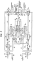
- Hereinafter, one embodiment of the present invention will be described with reference to Figure 7. This embodiment replaces the
conventional failure memory 5 of Figures 1 and 2, and has two redundant lines in each of the X and Y directions, i.e., N = 2 and Ny = 2. First, the structure of this embodiment will be described. - The structure can be broadly classified into the following three sections:
- (1) An address conversion unit which converts an
absolute X address 36 and anabsolute Y address 37 of a failure in a memory under test into x addresses 44, 46 and y addresses 45, 47 (48) in thecompressed data matrix 17. The address conversion unit includes the following members:- X and Y failure line registers
XFLR 20 andYFLR 21 which hold the X and Y addresses of the failures, respectively; - counters 22, 23 which count the number of new failure line addresses generated, produce outputs 44, 45 indicating whether or not the address numbers x, y of the
compressed data matrix 17 are within 6x6 and, at the same time, number abso-lute X, Y addresses 36, 37 of the failures in accordance with the sequence in which they occurred and replace them as the address data of thecompressed data matrix 17; - X and Y address registers XAR 33 and
YAR 34 which hold the x and y addresses 44 and 45 replaced by thecounters - a
decoder 35 which converts they address 47 as a data input (48) to thecompressed data matrix 17.
- X and Y failure line registers
- (2) The compressed
data matrix 17 described with reference to Figure 6. - (3)
Comparators 28 and 29 which detect whether new failures addresses are outside the compressed data metrix size 6x6;- X and Y line failure counters
XFLC 24 andYLFC 25 which detect decisions on remedy lines; -
gates -
gates XLFC 24 andYLFC 25 from counting the same failure number twice when a failure is found at the same address by different test patterns or the like.
- X and Y line failure counters
- Hereinafter, the operation of each of the three sections mentioned above will be described in detail.
- (1) The failure
line register XFLR 20 which registers the X address of a failure is a line memory (a RAM with a one-bit width and a depth the same as the X address length of the memory under test), as shown in Figure 8, inputs an output (X address) 40 from amultiplexer MUX 18 and writes the data "1" into that address. (It is assumed, of course, that initially all the memories and registers including the failureline register XFLR 20 have been cleared to "0".) If the input it receives is an address that has not already been written (to which access has not yet been made), the output of the failureline register XFLR 20 becomes "0", so that thecounter 22 in the next stage is incremented by one. In other words, the counter counts one whenever ENB is "0". If the address is one to which "1" has already been written (to which access has already been made at least once), on the other hand, theoutput 42 of the failureline register XFLR 20 becomes "1", so that thecounter 22 does not operate. - In this manner, six different failure addresses from 1 to 6 (or from 0 to 5) are stored in the X
address register XAR 33 in accordance with the sequence in which the failures occurred, so as to correspond to absolute X addresses 40. It is therefore possible to know which parts of the X addresses are stored by searching the X addresses 40 and examining the output (46) of the Xadress register XAR 33. - The operation described above also occurs on the Y side. The y addresses of the
compressed data matrix 17 converted and stored on the Y side are input to thedecoder 35 so they can be used as-a data input Din (48) to thecompressed data matrix 17. - (2) The structure of the
compressed data matrix 17 is illustrated in Figure 10. In order to constitute a 6x6 matrix accessed by x and y, this embodiment employs a RAM structure with 6 inputs and a depth of 6. The x data (x addresses 46) is used as address inputs, while the y data (decoder outputs 48) is used as data input. In order to represetn binary data up to a maximum value of 6, the data obtained from the 3-bit counter 22 is input unchanged as the x addresses 46, since the address decoder is within the RAM. When this matrix is read out for data analysis, therefore, the X addresses 38 corresponding to the x addresses 44, 46 examined in advance, as described above, are input from the CPU through themultiplexer MUX 18, and the compresseddata matrix output 49 is produced from Dout of Figure 10. In this case, the CPU completes the read-out by reading 6-bit,parallel data only 6 times. It is of course possible to replace the addresses of thecompressed data matrix 17 and Din by the y and x addresses, respectively, then input the Y addresses 39 to amultiplexer MUX 19 and read out the data. (3) As described above, when three or more failures are aligned on the same line in a memory under test which has redundant lines N x = 2 and N y = 2, that line is decided on as a remedy line, whether or not the failures are within the compressed data matrix. That is why the X and Y line failure countersXLFC 24 andYLFC 25 are provided on the X and Y sides to count the failures on a line. Figure 9 shows this structure for just the X linefailure counter XLFC 24. This is a two-stage shift register which usesRAMs XFLR 20 andYFLR 21, instead of counters. The counter provides the outputs of the double-count prevention gates RAMs RAM 59 to RAM 60 whenever the same address is held in the failure line registersXLFR 20,YFLR 21. - If the failure
line register XFLR 20 is considered to be a first stage,RAM 59 andRAM 60 can be regarded as the second and third stages, respectively. The alignment of three failures on the same line means that the output fromRAM 60 in the third stage at that address has become "1," and it can be understood, as shown in Figure 9, that the output can be used as such as an x remedy-decision flag 52. - In the actual analysis, the X addresses 38 are input from the CPU through the
multiplexer MUX 18, and it is possible to check their correspondence with the x addresses and, at the same time, obtain all the lines for which a remedy decision has been made from the output of theRAM 60 during the test. When the number of these lines exceeds the number of lines prepared as redundant lines, a judgement that remedy is impossible is immediately made, without the necessity of any analysis. - The
comparators 28 and 29 of Figure 7produce outputs 54 and 55, respectively, when the number of the corresponding stored x and y addresses 44 and 45 exceeds 6. As can be understood from the example of Ⓑ in Figure 6, it is necessary to check the remedy-decision flag on the x side so that x2 is determined to be a remedy line when the number exceeds thematrix 17 on the y side. Accordingly, an inhibition is applied to the comparator output 55 on the y side by the x remedy-decision flag 52. If thisflag 52 is not raised, the memory under test can not be remedied, and amemory NG flag 58 is output through the gate. The example of Figure 6@ shows a pattern for which "NG" is generated in this way. In other words, there are only two failures inclusive of Ⓑ on Y3 on the y side, and remedy is not decided on. - As described above, this embodiment compresses the analysis data for the remedy judgement into a matrix of only 6x6, which is determined by the number of redundant lines, simultaneously with completion of the test, irrespective of the sized of the memory under test, and can drastically reduce the time required for reading and analyzing the data. During the test, too, this embodiment makes it possible to identify those memories being tested for which a remedy is not possible, and redundant lines can be decided on without the need of analysis, depending upon the pattern of the failure occurrences. This also results in a reduction of the analysis time. Moreover, in comparison with the prior art which uses a memory of the same capacity as that of the memory being tested as a failure memory, the embodiment makes it possible to greatly reduce the hardware construction becuase it is constituted by the
compressed data matrix 17 of an extremely small capacity, and 1-bit wide memories such as the failure line registersXFLRs XLFC 24,YLFC 25, the address registersXAR 33,YAR 34, etc. Various matrix sizes can be realized easily according to the number of redundant lines, in the same way as in this embodiment. - The analysis time and capacity can be further improved by adding only the following limited quantities of hardware and memories to the structure of Figure 7, although they are not shown in the drawing for the sake of simplicity.
- If these are provided in the output stages of the X, Y line failure counters
XLFC 24,YLFC 25, a remedy- impossible judgement can be made immediately the number of remedy-decision lines exceeds the number of redundant lines. - These are memories which also store subsequent failure data as data for the analysis on the address lines which have been decided on as remedy lines by the X, Y failure counters
XLFC 24,YLFC 25. They can easily be realized by using the outputs of the remedy-decision flags - If these memories are provided, all the failure data within the memories which can be remedied is left, so that a higher degree of failure analysis and remedy judgement including a greater number of conditions can be made.
- Figures 11 through 14 illustrate concretely the disposition and method of construction of remedy-decision line memories, with reference to the compressed data matrix size (6x6) of Figure 6 by way of example.
- Figure 11 shows an example which is provided with two remedy-
decision line memories decision line memories - Figure 12 illustrates an example in which two
line memories - Figure 13 shows an example in which the x side of Figure 12 is replaced by the y side, and which is provided with
line memories memory 17". - Figure 14 shows an example in which memories on both x and y sides also function as the compressed data matrix.
- As described above, various constructions may be employed for the remedy-decision line memories. If memories are used which can also function as the compressed data matrix, however, the construction has the characterizing feature in that, since the compression is not effected by hardware, the quantity of analysis processing effected by the software after the completion of test is increased considerably, but the hardware required is less than that for the construction shown in Figure 11. This construction can be selected according to the processing time required.
- An embodiment of the present invention and additional constituents providing greater effects or higher functions have been-described above. However, a plurality of apparatuses based upon the analysis method of this invention may be provided parallel to one another when remedy judgement is necessary not only for memories which have 1-bit data lines, but also for those having so-called multi-data input-output (e.g., 4-bit or 8-bit). Furthermore, the construction applicable to such memories with different numbers of data bits can be realized easily by making a few modifications, primarily to the
counters - The X, Y line failure counters
XLFC 24 andYLFC 25 of Figure 7 can be replaced by ordinary shift registers or counters. - For memories which have redundant lines only on one side, not on both the X and Y sides, defects can be remedied by using only the output of the failure
line register XFLR 20 orYFLR 21 of Figure 7, and hence the present invention can be applied to both of these systems. - The present invention tests memories of a redundant line-defect remedy system, and can compress data thereon into a data matrix of a small capacity leaving only failure data for which a remedy judgement analysis is necessary, on the basis of test results. Accordingly, the present invention can drastically reduce analysis time as well as hardware size.
- Assume that the 64Kx1-bit memory with N = 2 and N = 2 redundant lines of Figure 6 is tested and the test results are compared with those of a test using a conventional failure memory of the same memory capacity. Assume also that the data is read in a 16-bit width for the conventional failure memory, and this read time is substantially proportional to the analysis time. In the embodiment of this invention shown in Figure 7, the compressed data matrix (6x6) is read in a 6-bit width. It can be thus understood that the time required is reduced to about 1/670 [i.e. (64K/16)/(36/6)≒667] required conventionally.
Claims (12)
Applications Claiming Priority (6)
| Application Number | Priority Date | Filing Date | Title |
|---|---|---|---|
| JP58080898A JPS59207497A (en) | 1983-05-11 | 1983-05-11 | Memory data compressing system |
| JP80897/83 | 1983-05-11 | ||
| JP58080899A JPS59207498A (en) | 1983-05-11 | 1983-05-11 | Tester of semiconductor memory |
| JP80899/83 | 1983-05-11 | ||
| JP80898/83 | 1983-05-11 | ||
| JP58080897A JPS59207496A (en) | 1983-05-11 | 1983-05-11 | Relief and analysis system for memory defective bit |
Publications (3)
| Publication Number | Publication Date |
|---|---|
| EP0125633A2 true EP0125633A2 (en) | 1984-11-21 |
| EP0125633A3 EP0125633A3 (en) | 1987-08-05 |
| EP0125633B1 EP0125633B1 (en) | 1990-08-08 |
Family
ID=27303418
Family Applications (1)
| Application Number | Title | Priority Date | Filing Date |
|---|---|---|---|
| EP84105285A Expired EP0125633B1 (en) | 1983-05-11 | 1984-05-10 | Testing apparatus for redundant memory |
Country Status (3)
| Country | Link |
|---|---|
| US (1) | US4628509A (en) |
| EP (1) | EP0125633B1 (en) |
| DE (1) | DE3482901D1 (en) |
Cited By (2)
| Publication number | Priority date | Publication date | Assignee | Title |
|---|---|---|---|---|
| EP0485976A2 (en) * | 1990-11-13 | 1992-05-20 | Kabushiki Kaisha Toshiba | Fault analysis apparatus for memories having redundancy circuits |
| GB2292236A (en) * | 1995-04-04 | 1996-02-14 | Memory Corp Plc | Improved partial memory engine |
Families Citing this family (32)
| Publication number | Priority date | Publication date | Assignee | Title |
|---|---|---|---|---|
| JPS60210000A (en) * | 1984-04-04 | 1985-10-22 | Hitachi Ltd | Fail memory |
| US4751656A (en) * | 1986-03-10 | 1988-06-14 | International Business Machines Corporation | Method for choosing replacement lines in a two dimensionally redundant array |
| EP0424612A3 (en) * | 1989-08-30 | 1992-03-11 | International Business Machines Corporation | Apparatus and method for real time data error capture and compression for redundancy analysis of a memory |
| US5161158A (en) * | 1989-10-16 | 1992-11-03 | The Boeing Company | Failure analysis system |
| JP3316876B2 (en) * | 1992-06-30 | 2002-08-19 | 安藤電気株式会社 | Address generation circuit for data compression |
| JP3240709B2 (en) * | 1992-10-30 | 2001-12-25 | 株式会社アドバンテスト | Memory test equipment |
| FR2699301B1 (en) * | 1992-12-16 | 1995-02-10 | Sgs Thomson Microelectronics | Method for treating defective elements in a memory. |
| US5588115A (en) * | 1993-01-29 | 1996-12-24 | Teradyne, Inc. | Redundancy analyzer for automatic memory tester |
| JPH0816486A (en) * | 1994-06-29 | 1996-01-19 | Hitachi Ltd | Lsi for defect remedy and memory device |
| US5795797A (en) * | 1995-08-18 | 1998-08-18 | Teradyne, Inc. | Method of making memory chips using memory tester providing fast repair |
| US5631868A (en) * | 1995-11-28 | 1997-05-20 | International Business Machines Corporation | Method and apparatus for testing redundant word and bit lines in a memory array |
| US5754556A (en) * | 1996-07-18 | 1998-05-19 | Teradyne, Inc. | Semiconductor memory tester with hardware accelerators |
| US5983374A (en) * | 1996-09-26 | 1999-11-09 | Kabushiki Kaisha Toshiba | Semiconductor test system and method, and medium for recording test program therefor |
| JP3547064B2 (en) * | 1996-10-23 | 2004-07-28 | 株式会社アドバンテスト | Memory test equipment |
| GB9623215D0 (en) * | 1996-11-07 | 1997-01-08 | Process Insight Limited | Solid state memory test system with defect compression |
| US6360340B1 (en) * | 1996-11-19 | 2002-03-19 | Teradyne, Inc. | Memory tester with data compression |
| JP3558252B2 (en) * | 1997-11-10 | 2004-08-25 | 株式会社アドバンテスト | Semiconductor memory test equipment |
| US6138254A (en) * | 1998-01-22 | 2000-10-24 | Micron Technology, Inc. | Method and apparatus for redundant location addressing using data compression |
| US6442724B1 (en) | 1999-04-02 | 2002-08-27 | Teradyne, Inc. | Failure capture apparatus and method for automatic test equipment |
| JP2000348498A (en) * | 1999-06-08 | 2000-12-15 | Mitsubishi Electric Corp | Semiconductor testing apparatus |
| US6735729B1 (en) * | 1999-08-18 | 2004-05-11 | Micron Technology, Inc | Compression circuit for testing a memory device |
| US6536005B1 (en) * | 1999-10-26 | 2003-03-18 | Teradyne, Inc. | High-speed failure capture apparatus and method for automatic test equipment |
| JP2002343098A (en) * | 2001-05-18 | 2002-11-29 | Mitsubishi Electric Corp | Test method for semiconductor memory |
| JP2003346496A (en) * | 2002-05-22 | 2003-12-05 | Mitsubishi Electric Corp | Defective information storage, defective information storage processor provided with the same, defective information storage method, semiconductor device testing apparatus provided with defective information storage, and semiconductor device provided with defective information storage |
| TW578160B (en) * | 2002-11-29 | 2004-03-01 | Via Tech Inc | Memory modeling circuit with fault tolerant |
| US7493534B2 (en) * | 2003-08-29 | 2009-02-17 | Hewlett-Packard Development Company, L.P. | Memory error ranking |
| US7574640B2 (en) * | 2003-09-05 | 2009-08-11 | Intel Corporation | Compacting circuit responses |
| US7484065B2 (en) | 2004-04-20 | 2009-01-27 | Hewlett-Packard Development Company, L.P. | Selective memory allocation |
| US8977912B2 (en) * | 2007-05-07 | 2015-03-10 | Macronix International Co., Ltd. | Method and apparatus for repairing memory |
| US8799732B2 (en) * | 2012-02-09 | 2014-08-05 | International Business Machines Corporation | Methodology for correlated memory fail estimations |
| JP6715198B2 (en) * | 2017-02-20 | 2020-07-01 | キオクシア株式会社 | Memory inspection device |
| DE102020134945A1 (en) * | 2020-02-27 | 2021-09-02 | Taiwan Semiconductor Manufacturing Co., Ltd. | DYNAMIC FAULT MONITORING AND REPAIR |
Citations (1)
| Publication number | Priority date | Publication date | Assignee | Title |
|---|---|---|---|---|
| US4369511A (en) * | 1979-11-21 | 1983-01-18 | Nippon Telegraph & Telephone Public Corp. | Semiconductor memory test equipment |
Family Cites Families (9)
| Publication number | Priority date | Publication date | Assignee | Title |
|---|---|---|---|---|
| US4232375A (en) * | 1978-06-12 | 1980-11-04 | Ncr Corporation | Data compression system and apparatus |
| US4335447A (en) * | 1980-02-05 | 1982-06-15 | Sangamo Weston, Inc. | Power outage recovery method and apparatus for demand recorder with solid state memory |
| FR2491703B1 (en) * | 1980-10-03 | 1988-04-29 | Thomson Csf | COMPRESSION DEVICE AND TEMPORAL DATA DECOMPRESSION DEVICE AND TRANSMISSION SYSTEM COMPRISING AT LEAST ONE OF SUCH DEVICES |
| US4380066A (en) * | 1980-12-04 | 1983-04-12 | Burroughs Corporation | Defect tolerant memory |
| US4412306A (en) * | 1981-05-14 | 1983-10-25 | Moll Edward W | System for minimizing space requirements for storage and transmission of digital signals |
| US4460999A (en) * | 1981-07-15 | 1984-07-17 | Pacific Western Systems, Inc. | Memory tester having memory repair analysis under pattern generator control |
| US4460997A (en) * | 1981-07-15 | 1984-07-17 | Pacific Western Systems Inc. | Memory tester having memory repair analysis capability |
| US4400794A (en) * | 1981-11-17 | 1983-08-23 | Burroughs Corporation | Memory mapping unit |
| US4464747A (en) * | 1982-02-18 | 1984-08-07 | The Singer Company | High reliability memory |
-
1984
- 1984-05-10 DE DE8484105285T patent/DE3482901D1/en not_active Expired - Lifetime
- 1984-05-10 EP EP84105285A patent/EP0125633B1/en not_active Expired
- 1984-05-11 US US06/609,445 patent/US4628509A/en not_active Expired - Fee Related
Patent Citations (1)
| Publication number | Priority date | Publication date | Assignee | Title |
|---|---|---|---|---|
| US4369511A (en) * | 1979-11-21 | 1983-01-18 | Nippon Telegraph & Telephone Public Corp. | Semiconductor memory test equipment |
Non-Patent Citations (1)
| Title |
|---|
| IEEE 1981 INTERNATIONAL TEST CONFERENCE, DIGEST OF PAPERS, 27th - 29th October 1981, Philadelphia, US, Paper 3,4, pages 49-55, IEEE; R.C. EVANS: "Testing repairable RAMs and mostly good memories" * |
Cited By (4)
| Publication number | Priority date | Publication date | Assignee | Title |
|---|---|---|---|---|
| EP0485976A2 (en) * | 1990-11-13 | 1992-05-20 | Kabushiki Kaisha Toshiba | Fault analysis apparatus for memories having redundancy circuits |
| EP0485976A3 (en) * | 1990-11-13 | 1993-04-14 | Kabushiki Kaisha Toshiba | Fault analysis apparatus for memories having redundancy circuits |
| US5363382A (en) * | 1990-11-13 | 1994-11-08 | Kabushiki Kaisha Toshiba | Fault analysis apparatus for memories having redundancy circuits |
| GB2292236A (en) * | 1995-04-04 | 1996-02-14 | Memory Corp Plc | Improved partial memory engine |
Also Published As
| Publication number | Publication date |
|---|---|
| DE3482901D1 (en) | 1990-09-13 |
| US4628509A (en) | 1986-12-09 |
| EP0125633A3 (en) | 1987-08-05 |
| EP0125633B1 (en) | 1990-08-08 |
Similar Documents
| Publication | Publication Date | Title |
|---|---|---|
| US4628509A (en) | Testing apparatus for redundant memory | |
| US7370251B2 (en) | Method and circuit for collecting memory failure information | |
| KR100444427B1 (en) | Semiconductor memory manufacturing system | |
| KR100271431B1 (en) | Memory testing apparatus | |
| US6360340B1 (en) | Memory tester with data compression | |
| US6421794B1 (en) | Method and apparatus for diagnosing memory using self-testing circuits | |
| JP3558252B2 (en) | Semiconductor memory test equipment | |
| JPH0752599B2 (en) | Device and method for capturing and compressing memory fault information | |
| US20030005353A1 (en) | Methods and apparatus for storing memory test information | |
| JPH09318707A (en) | Method and apparatus for test of semiconductor memory | |
| JPH1116393A (en) | Test circuit | |
| US7688658B2 (en) | Semiconductor device in which a plurality of memory macros are mounted, and testing method thereof | |
| US6711705B1 (en) | Method of analyzing a relief of failure cell in a memory and memory testing apparatus having a failure relief analyzer using the method | |
| US20090094494A1 (en) | Semiconductor integrated circuit and method of testing same | |
| US6687862B1 (en) | Apparatus and method for fast memory fault analysis | |
| JPS6233626B2 (en) | ||
| JP2001256798A (en) | Semiconductor test device, semiconductor test method, and machine readable recording medium in which program is recorded | |
| JP2622720B2 (en) | Fail bit analysis method | |
| JPH03720B2 (en) | ||
| JPH11297094A (en) | Semiconductor tester | |
| KR19990029646A (en) | Memory tester | |
| JP3186126B2 (en) | Semiconductor test equipment and semiconductor test system | |
| JPS6168800A (en) | Memory test equipment | |
| JPH09147596A (en) | Semiconductor testing device | |
| JPS59207498A (en) | Tester of semiconductor memory |
Legal Events
| Date | Code | Title | Description |
|---|---|---|---|
| PUAI | Public reference made under article 153(3) epc to a published international application that has entered the european phase |
Free format text: ORIGINAL CODE: 0009012 |
|
| 17P | Request for examination filed |
Effective date: 19840510 |
|
| AK | Designated contracting states |
Designated state(s): DE FR GB |
|
| PUAL | Search report despatched |
Free format text: ORIGINAL CODE: 0009013 |
|
| AK | Designated contracting states |
Kind code of ref document: A3 Designated state(s): DE FR GB |
|
| 17Q | First examination report despatched |
Effective date: 19880511 |
|
| GRAA | (expected) grant |
Free format text: ORIGINAL CODE: 0009210 |
|
| AK | Designated contracting states |
Kind code of ref document: B1 Designated state(s): DE FR GB |
|
| REF | Corresponds to: |
Ref document number: 3482901 Country of ref document: DE Date of ref document: 19900913 |
|
| ET | Fr: translation filed | ||
| PLBE | No opposition filed within time limit |
Free format text: ORIGINAL CODE: 0009261 |
|
| STAA | Information on the status of an ep patent application or granted ep patent |
Free format text: STATUS: NO OPPOSITION FILED WITHIN TIME LIMIT |
|
| 26N | No opposition filed | ||
| PGFP | Annual fee paid to national office [announced via postgrant information from national office to epo] |
Ref country code: GB Payment date: 19940429 Year of fee payment: 11 |
|
| PGFP | Annual fee paid to national office [announced via postgrant information from national office to epo] |
Ref country code: FR Payment date: 19940516 Year of fee payment: 11 |
|
| PG25 | Lapsed in a contracting state [announced via postgrant information from national office to epo] |
Ref country code: GB Effective date: 19950510 |
|
| GBPC | Gb: european patent ceased through non-payment of renewal fee |
Effective date: 19950510 |
|
| PG25 | Lapsed in a contracting state [announced via postgrant information from national office to epo] |
Ref country code: FR Effective date: 19960229 |
|
| REG | Reference to a national code |
Ref country code: FR Ref legal event code: ST |
|
| REG | Reference to a national code |
Ref country code: FR Ref legal event code: ST |
|
| PGFP | Annual fee paid to national office [announced via postgrant information from national office to epo] |
Ref country code: DE Payment date: 19960626 Year of fee payment: 13 |
|
| PG25 | Lapsed in a contracting state [announced via postgrant information from national office to epo] |
Ref country code: DE Free format text: LAPSE BECAUSE OF NON-PAYMENT OF DUE FEES Effective date: 19980203 |