EP0180978A2 - Electronic cash register - Google Patents
Electronic cash register Download PDFInfo
- Publication number
- EP0180978A2 EP0180978A2 EP85114137A EP85114137A EP0180978A2 EP 0180978 A2 EP0180978 A2 EP 0180978A2 EP 85114137 A EP85114137 A EP 85114137A EP 85114137 A EP85114137 A EP 85114137A EP 0180978 A2 EP0180978 A2 EP 0180978A2
- Authority
- EP
- European Patent Office
- Prior art keywords
- stored
- volatile memory
- data
- eprom
- code
- Prior art date
- Legal status (The legal status is an assumption and is not a legal conclusion. Google has not performed a legal analysis and makes no representation as to the accuracy of the status listed.)
- Granted
Links
Images


Classifications
-
- G—PHYSICS
- G07—CHECKING-DEVICES
- G07G—REGISTERING THE RECEIPT OF CASH, VALUABLES, OR TOKENS
- G07G1/00—Cash registers
- G07G1/12—Cash registers electronically operated
-
- G—PHYSICS
- G06—COMPUTING; CALCULATING OR COUNTING
- G06Q—INFORMATION AND COMMUNICATION TECHNOLOGY [ICT] SPECIALLY ADAPTED FOR ADMINISTRATIVE, COMMERCIAL, FINANCIAL, MANAGERIAL OR SUPERVISORY PURPOSES; SYSTEMS OR METHODS SPECIALLY ADAPTED FOR ADMINISTRATIVE, COMMERCIAL, FINANCIAL, MANAGERIAL OR SUPERVISORY PURPOSES, NOT OTHERWISE PROVIDED FOR
- G06Q20/00—Payment architectures, schemes or protocols
- G06Q20/08—Payment architectures
- G06Q20/20—Point-of-sale [POS] network systems
- G06Q20/201—Price look-up processing, e.g. updating
Definitions
- the present invention relates to an electronic cash register.
- various data associated with the cash registration are stored in a volatile memory that requires the constant supply of an electric power.
- the memory In order that such data as to be registered for a predetermined period of time, for example, for several days, are to be stored in the volatile memory, the memory must be powered by electricity event when the cash register is not operated. In the even that the commercial electric power supply is interrupted by any reason, the volatile memory is powered by an auxiliary back-up power source, for example, a battery, to protect the once-stored data from being volatilized.
- the present invention has for its essential object to provide an improved electronic cash register wherein improvement has been made to enable data stored in a memory used therein to be retained assuredly for a long period of time without being destroyed, thereby to increase the reliability of the electronic cash register.
- Another important object of the present invention is to provide an improved cash register of the type referred to above wherein the the reliability of the data stored in the volatile memory in connection with the cash register is increased.
- the present invention provides an electronic cash register which comprises a volatile memory for the storage of data concerned of cash registration, a writable non-volatile memory for the storage of said data, a control means for writing said data in said non-volatile memory, means for correcting the contents, stored in the volatile memory, on the basis of the data stored in the non-volatile memory, and means for displaying the contents stored in the volatile memory and the contents stored in the non-volatile memory.
- the present invention provides an electronic cash register which comprises a volatile memory for the storage of data concerned with cash registration, a writable non-volatile memory, detachably mounted in the cash register and having a data area for storing information associated with said data and a code area for storing identification codes, and a processing means for correcting the contents, stored in the volatile memory, on the basis of the information stored in the non-volatile memory, and operable to, in the even that no identification code is stored in the code area, storing a predetermined identification code in the code area to write data in the data area and to, in the event that the identification code is stored in the code area, compare the stored identification code with the predetermined code, data being written in the data area only when the stored identification code coincides with the predetermined code.
- an electronic cash register is provided with a keyboard input device 2 for entering instructions associated with registration and adjustment of money, a display unit 3 for displaying numerical figures inputted from the keyboard 2, and a printer unit 4 for printing data on a paper slip or the like.
- a central processing unit 5, hereinafter referred to as CPU performs a procedure according to a program, stored in a read-only memory (ROM) 6, when instructed by the command from the keyboard input device 2 and operates to store the result of the procedure in a random-access memory (RAM) 7 which is a volatile memory.
- ROM read-only memory
- RAM random-access memory
- EPROM erasable programmable read-only memory
- control unit 9 for controlling the write-in operation of EPROM 8 so that the result of the daily adjustment performed after the transaction of money for a particular day can be written in EPROM 8.
- E P ROM 8 is detachably provided in the above described system and can be replaced with another EPROM when the whole write-in areas of the first-used EPROM 8 have been occupied. Because of this, according to the present invention, in order to prevent data from being written in such another EPROM when the first-used EPROM has been replaced, the sequence of operation is carried out according to a flowchart shown in Fig. 2.
- ROM 6 stores a predetermined identification code, for example, a character "a", beforehand, and the same character as the character "a” has to be registered in EPROM 8. In this case, as shown in Fig. 2, a decision is made at step sl to determined if the character "a" has been registered in EPROM 8.
- This decision is carried out by a set flag b in a code area A (shown in Fig. 4) of EPROM 8. If the set flag b is "1", it is determined that the character "a” has not been registered, but if it is "0", it is determined that the character "a” has been registered. In the event that the set flag is "1", the predetermined character "a” stored in ROM 6 is stored in EPROM 8 at step s2. On the other hand, in the event that the set flag b is "0", a decision is made at step s3 to determine if the character stored in ROM 6 coincides with that stored in EPROM 8.
- the error handling procedure includes, for example, the display, by means of the display unit 3, of information indicative of non-coincidence of the characters and, during this procedure, the operator has to remove the EPROM 8 from the system and connect another EPROM 8 in which the character "a" is written.
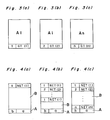
- Fig. 3 illustrates the contents stored in RAM 7, and Fig. 4 illustrates the contents stored in EPROM 8.
- data Al representative of the sales transaction for this day is stored in RAM 7 as shown in Fig. 3 (a) and, on the basis of this data, the total GT(1) and the amount NET(1) are calculated for this day.
- the total GT(1) is stored in RAM 7, and as shown in Fig. 4 (a), the total NET(l) is stored in EPROM 8.
- the counter value "1" is also stored in both of RAM 7 and EPROM 8.
- the amount NET(i) for this day is calculated on the basis of the data Ai and is then stored in EPROM 8 as shown in Fig. 4(b).
- the total GT(i) for this day which is the sum of the amount NET(i) and the total GT(i-1) for the preceding day is stored in EPROM 8 as shown in Fig. 3(b).
- the counter value i is stored in association with the amount NET(i), and within RAM 7, the counter value i-1 stored therein is incremented by one_and is then stored.
- the amount NET(n) is calculated on the basis of the data An2 for this day and is stored in EPROM 8 as shown in Fig.
- the total GT(n) which is the sum of the amount NET(n) for this day and the total GT(n-1) calculated until the preceding day, is stored in RAM 7 as shown in Fig. 3(c).
- the counter value n is stored in association with the amount NET(3), and within RAM 7, the counter value n-1 for the preceding day is incremented by one and the counter value n is stored.
- the contents stored in RAM 7 and EPROM 8 in the manner as hereinabove described can be outputted to one or both of the display and printer units 3 and 4 by manipulating the keyboard unit 1.
- the display of the amounts NET(1) ... NET(n) and the counter values 1 ... i stored in EPROM 8 can be effected by setting a mode selecto: switch, provided in the keyboard unit 2, in a position, for example, a check mode position, at which the contents stored in EPROM 8 can be outputted, keying in a required period and finally keying in to command the outputting of the contents in EPROM 8.
- step nl the counter value for the preceding day stored in RAM 7 is checked against the counter value i-1 for the preceding day stored in EPROM 8. If the result of the decision at step nl indicates that the counter values stored in RAM 7 and EPROM 8 coincide with each other, the program flow proceeds to the next step n2, but if it indicates that they do not coincide, the error handling procedure is performed as will be described later.
- step n2 a decision is made to determine if the respective values of the amounts NET(I) ... NET(i-1) stored in EPROM 8 coincide with the total GT(i-1) stored in RA M 7 which had been calculated until the preceding day.
- step n3 a decision is made to determine if there is a write-in area in EPROM 8. If the result of decision at step n3 indicates that there is a write-in area in EPROM 8, the program flow proceeds to step n4, but if it indicates that there is no write-in area in ERPOM 8, the error handling procedure is performed. During the error handling procedure, the lack of the write-in area in EPROM 8 is displayed and this problem can be overcome when the operator expands ERPOM 8. At step n4, the counter value i for the particular day and the amount NET(i) are stored in ERPOM 8.
- the error handling procedure is performed to set a stop flag for bringing the cash register to a halt. Once the stop flag is set, the electronic cash register is blocked out with no input received thereby. Should the contents of RAM 7 be incorrect, the operator has to perform a master reset.
- the master reset is a procedure required to re-open the suspended procedure.
- Fig. 6 illustrates a flowchart for the error handling procedure to be followed when the contents stored in RAM 7 are incorrect.
- the master reset is carried out by depressing a reset key arranged in the keyboard unit 2.
- CPU 5 commands ERPO M 8 to transfer the counter value i - 1, stored in EPROM 8, to RA M 7 thereby modifying the counter value stored in RAM 7.
- the total GT (i) which is the sum of the amounts NE T (l) ... NET(i) stored in ERPOM 8 is transferred to RAM 7 and the total stored in RAM 7 is modified accordingly.
- the stop flag is released, allowing the cash register to assume its normal operation.
Abstract
Description
- The present invention relates to an electronic cash register.
- In an electronic cash register, various data associated with the cash registration are stored in a volatile memory that requires the constant supply of an electric power. In order that such data as to be registered for a predetermined period of time, for example, for several days, are to be stored in the volatile memory, the memory must be powered by electricity event when the cash register is not operated. In the even that the commercial electric power supply is interrupted by any reason, the volatile memory is powered by an auxiliary back-up power source, for example, a battery, to protect the once-stored data from being volatilized.
- Since any battery used for the back-up power source for continuously powering the volatile memory has a limited lifetime, and/or by any other reason, it may happen that the volatile memory will be no longer powered. Thus, according to the prior art, there is a problem in that the reliability to the data stored in the volatile memory for a long period of time is not so high.
- The present invention has for its essential object to provide an improved electronic cash register wherein improvement has been made to enable data stored in a memory used therein to be retained assuredly for a long period of time without being destroyed, thereby to increase the reliability of the electronic cash register.
- Another important object of the present invention is to provide an improved cash register of the type referred to above wherein the the reliability of the data stored in the volatile memory in connection with the cash register is increased.
- In order to accomplish these objects, the present invention provides an electronic cash register which comprises a volatile memory for the storage of data concerned of cash registration, a writable non-volatile memory for the storage of said data, a control means for writing said data in said non-volatile memory, means for correcting the contents, stored in the volatile memory, on the basis of the data stored in the non-volatile memory, and means for displaying the contents stored in the volatile memory and the contents stored in the non-volatile memory.
- With this construction, since the contents stored in the volatile memory can be corrected on the basis of the data stored in the non-volatile memory, the reliability of the contents stored in the volatile memory can be increased. Also, since both of the contents stored in the volatile and non-volatile memories, respectively, can be displayed, the contents stored in the respective memories can readily be confirmed.
- Moreover, the present invention provides an electronic cash register which comprises a volatile memory for the storage of data concerned with cash registration, a writable non-volatile memory, detachably mounted in the cash register and having a data area for storing information associated with said data and a code area for storing identification codes, and a processing means for correcting the contents, stored in the volatile memory, on the basis of the information stored in the non-volatile memory, and operable to, in the even that no identification code is stored in the code area, storing a predetermined identification code in the code area to write data in the data area and to, in the event that the identification code is stored in the code area, compare the stored identification code with the predetermined code, data being written in the data area only when the stored identification code coincides with the predetermined code.
- With this construction, since no data is written in the data area of the non-volatile memory when the identification code stored in the code area of such non-volatile memory does not coincide with the predetermined code, the reliability of the contents stored in the volatile memory can be increased.
- These and other objects and features of the present invention will become clear from the following description taken ,in conjunction with a preferred embodiment thereof with reference to the accompanying drawings, in which:
- Fig. 1 is a block diagram showing the circuitry of an electronic cash register;
- Fig. 2 is a flowchart showing the sequence of operation necessary to avoid any erroneous write-in of data in an erasable programmable read-only memory when the latter has been substituted for an erasable programmable read-only memory which has been utilized;
- Fig. 3 is an explanatory diagram used for the explanation of contents to be stored in a random-access memory;
- Fig. 4 is an explanatory diagram used for the explanation of contents to be stored in the erasable programmable read-only memory;
- Fig. 5 is a flowchart showing the sequence of operation necessary to determine if the contents stored in the random-access memory are correct; and
- Fig. 6 is a flowchart showing the sequence of operation of a central processing unit in the even that the contents stored in the random-access memory are not correct.
- Referring first to Fig. 1 an electronic cash register, generally identified by 1, is provided with a
keyboard input device 2 for entering instructions associated with registration and adjustment of money, adisplay unit 3 for displaying numerical figures inputted from thekeyboard 2, and aprinter unit 4 for printing data on a paper slip or the like. Acentral processing unit 5, hereinafter referred to as CPU, performs a procedure according to a program, stored in a read-only memory (ROM) 6, when instructed by the command from thekeyboard input device 2 and operates to store the result of the procedure in a random-access memory (RAM) 7 which is a volatile memory. - In accordance with the present invention, there is provided in association with
CPU 5, an erasable programmable read-only memory (hereinafter referred to as "EPROM") 8 which is a writable non-volatile memory, and acontrol unit 9 for controlling the write-in operation ofEPROM 8 so that the result of the daily adjustment performed after the transaction of money for a particular day can be written in EPROM 8. - EPROM 8 is detachably provided in the above described system and can be replaced with another EPROM when the whole write-in areas of the first-used EPROM 8 have been occupied. Because of this, according to the present invention, in order to prevent data from being written in such another EPROM when the first-used EPROM has been replaced, the sequence of operation is carried out according to a flowchart shown in Fig. 2.
ROM 6 stores a predetermined identification code, for example, a character "a", beforehand, and the same character as the character "a" has to be registered in EPROM 8. In this case, as shown in Fig. 2, a decision is made at step sl to determined if the character "a" has been registered in EPROM 8. This decision is carried out by a set flag b in a code area A (shown in Fig. 4) of EPROM 8. If the set flag b is "1", it is determined that the character "a" has not been registered, but if it is "0", it is determined that the character "a" has been registered. In the event that the set flag is "1", the predetermined character "a" stored inROM 6 is stored in EPROM 8 at step s2. On the other hand, in the event that the set flag b is "0", a decision is made at step s3 to determine if the character stored inROM 6 coincides with that stored in EPROM 8. If the result of decision at step s3 indicates that the characters inROM 6 andERPOM 8 coincide with each other, such data as will be described later are stored in a data area B (shown in Fig. 4) ofEPROM 8, but if it indicates that they do not coincide with each other, an error handling procedure is carried out. The error handling procedure includes, for example, the display, by means of thedisplay unit 3, of information indicative of non-coincidence of the characters and, during this procedure, the operator has to remove theEPROM 8 from the system and connect anotherEPROM 8 in which the character "a" is written. - Hereinafter, contents stored in
RAM 7 and EPROM 8 will be described. Let it be assumed that the counter value representative of a predetermined period of time during which the daily adjustment of sales is carried out is expressed by n, and a counter value representative of the number of times the daily adjustment has been carried out is expressed by i. It is also assumed that the daily amount of sales determined by the daily adjustment for each day is expressed by NET(i) and the total of the amounts of sales during the predetermined period is expressed by GT(i). These parameters have a particular relationship expressed by the following equation:
- Fig. 3 illustrates the contents stored in
RAM 7, and Fig. 4 illustrates the contents stored in EPROM 8. On the first day of the predetermined period, data Al representative of the sales transaction for this day is stored inRAM 7 as shown in Fig. 3 (a) and, on the basis of this data, the total GT(1) and the amount NET(1) are calculated for this day. As shown in Fig. 3(a), the total GT(1) is stored inRAM 7, and as shown in Fig. 4 (a), the total NET(l) is stored in EPROM 8. At this time, the counter value "1" is also stored in both ofRAM 7 and EPROM 8. On the i-th day during the predetermined period, the amount NET(i) for this day is calculated on the basis of the data Ai and is then stored inEPROM 8 as shown in Fig. 4(b). The total GT(i) for this day, which is the sum of the amount NET(i) and the total GT(i-1) for the preceding day is stored in EPROM 8 as shown in Fig. 3(b). Within EPROM 8, the counter value i is stored in association with the amount NET(i), and withinRAM 7, the counter value i-1 stored therein is incremented by one_and is then stored. On the n-th day during the period, the amount NET(n) is calculated on the basis of the data An2 for this day and is stored inEPROM 8 as shown in Fig. 4(c). Then, the total GT(n) which is the sum of the amount NET(n) for this day and the total GT(n-1) calculated until the preceding day, is stored inRAM 7 as shown in Fig. 3(c). Within the EPROM 8, the counter value n is stored in association with the amount NET(3), and withinRAM 7, the counter value n-1 for the preceding day is incremented by one and the counter value n is stored. - The contents stored in
RAM 7 and EPROM 8 in the manner as hereinabove described can be outputted to one or both of the display andprinter units keyboard unit 1. By way of example, the display of the amounts NET(1) ... NET(n) and thecounter values 1 ... i stored in EPROM 8 can be effected by setting a mode selecto: switch, provided in thekeyboard unit 2, in a position, for example, a check mode position, at which the contents stored in EPROM 8 can be outputted, keying in a required period and finally keying in to command the outputting of the contents inEPROM 8. - When the daily amounts NET(I) of sales are summed and stored in EPROM 8, a decision is made to determine if the contents stored in
RAM 7 are correct. A flowchart necessary to achieve this decision is shown in Fig. 5, it being to be noted that the following description made with reference to Fig. 5 is associated with the procedure to be done on the i-th day of the predetermined period. - Referring to Fig. 5, at step nl, the counter value for the preceding day stored in
RAM 7 is checked against the counter value i-1 for the preceding day stored in EPROM 8. If the result of the decision at step nl indicates that the counter values stored inRAM 7 and EPROM 8 coincide with each other, the program flow proceeds to the next step n2, but if it indicates that they do not coincide, the error handling procedure is performed as will be described later. At step n2, a decision is made to determine if the respective values of the amounts NET(I) ... NET(i-1) stored in EPROM 8 coincide with the total GT(i-1) stored in RAM 7 which had been calculated until the preceding day. If the total GT(i) is found coinciding, the next succeeding step n3 takes place, but if it is found not coinciding, the error handling procedure is performed. At step n3, a decision is made to determine if there is a write-in area in EPROM 8. If the result of decision at step n3 indicates that there is a write-in area inEPROM 8, the program flow proceeds to step n4, but if it indicates that there is no write-in area inERPOM 8, the error handling procedure is performed. During the error handling procedure, the lack of the write-in area inEPROM 8 is displayed and this problem can be overcome when the operator expandsERPOM 8. At step n4, the counter value i for the particular day and the amount NET(i) are stored inERPOM 8. - On the other hand, when the counter values have been found not coinciding with each other at step nl indicating that the contents stored in
RAM 7 are incorrect, or when the values have been found not coinciding with each other at step n2 indicating that the total GT(i-1) stored inRAM 7 is incorrect, the error handling procedure is performed to set a stop flag for bringing the cash register to a halt. Once the stop flag is set, the electronic cash register is blocked out with no input received thereby. Should the contents ofRAM 7 be incorrect, the operator has to perform a master reset. The master reset is a procedure required to re-open the suspended procedure. - Fig. 6 illustrates a flowchart for the error handling procedure to be followed when the contents stored in
RAM 7 are incorrect. The master reset is carried out by depressing a reset key arranged in thekeyboard unit 2. When the reset key is depressed,CPU 5 commandsERPO M 8 to transfer thecounter value i -1, stored inEPROM 8, toRA M 7 thereby modifying the counter value stored inRAM 7. At step m2, the total GT (i) which is the sum of the amounts NET(l) ... NET(i) stored inERPOM 8 is transferred toRAM 7 and the total stored inRAM 7 is modified accordingly. At step m3, the stop flag is released, allowing the cash register to assume its normal operation. - As hereinbefore described, since whether or not the contents stored in
RAM 7 are correct is determined on the basis of the contents stored inEPROM 8, a correct procedure can be continued with high reliability even though the contents stored inRAM 7 are changed or destroyed. Thus, since the identification code of the non-volatile memory loaded in the system can be checked and the contents stored in the volatile memory can be confirmed, the reliability of the contents of the volatile memory can be increased. - Although the present invention has been fully described by way of example with reference to the accompanying drawings, it is to be noted here that various changes and modifications will be apparent to those skilled in the art. Therefore, unless otherwise such changes and modifications depart from the scope of the present invention, they should be construed as being included therein.
Claims (2)
Applications Claiming Priority (4)
| Application Number | Priority Date | Filing Date | Title |
|---|---|---|---|
| JP168831/84 | 1984-11-07 | ||
| JP1984168831U JPH0222777Y2 (en) | 1984-11-07 | 1984-11-07 | |
| JP170843/84 | 1984-11-09 | ||
| JP1984170843U JPH0348700Y2 (en) | 1984-11-09 | 1984-11-09 |
Publications (3)
| Publication Number | Publication Date |
|---|---|
| EP0180978A2 true EP0180978A2 (en) | 1986-05-14 |
| EP0180978A3 EP0180978A3 (en) | 1988-08-17 |
| EP0180978B1 EP0180978B1 (en) | 1992-10-14 |
Family
ID=26492373
Family Applications (1)
| Application Number | Title | Priority Date | Filing Date |
|---|---|---|---|
| EP85114137A Expired - Lifetime EP0180978B1 (en) | 1984-11-07 | 1985-11-06 | Electronic cash register |
Country Status (3)
| Country | Link |
|---|---|
| US (1) | US4853853A (en) |
| EP (1) | EP0180978B1 (en) |
| DE (1) | DE3586756T2 (en) |
Cited By (6)
| Publication number | Priority date | Publication date | Assignee | Title |
|---|---|---|---|---|
| EP0373732A2 (en) * | 1988-12-16 | 1990-06-20 | MANNESMANN Aktiengesellschaft | Multi-function printer with a journal printing device |
| WO1996013012A1 (en) * | 1994-10-19 | 1996-05-02 | Siemens Nixdorf Informationssysteme Ag | Journal store |
| GB2297414A (en) * | 1995-01-25 | 1996-07-31 | Ravell Holdings Pte Ltd | Point of sale system |
| WO1999066465A1 (en) * | 1998-06-17 | 1999-12-23 | Zpm - Indústria, Comércio, Importação, Exportação E Representações Ltda. | Disposition in fiscal printer |
| US7523320B2 (en) | 2003-04-22 | 2009-04-21 | Seiko Epson Corporation | Fiscal data recorder with protection circuit and tamper-proof seal |
| WO2012067169A1 (en) | 2010-11-19 | 2012-05-24 | Seiko Epson Corporation | Fiscal memory control method, fiscal control circuit board, and fiscal printer |
Families Citing this family (6)
| Publication number | Priority date | Publication date | Assignee | Title |
|---|---|---|---|---|
| DE69034227T2 (en) | 1989-04-13 | 2007-05-03 | Sandisk Corp., Sunnyvale | EEprom system with block deletion |
| US5263164A (en) | 1991-01-09 | 1993-11-16 | Verifone, Inc. | Method and structure for determining transaction system hardware and software configurations |
| US20030195848A1 (en) | 1996-06-05 | 2003-10-16 | David Felger | Method of billing a purchase made over a computer network |
| US7555458B1 (en) | 1996-06-05 | 2009-06-30 | Fraud Control System.Com Corporation | Method of billing a purchase made over a computer network |
| US8229844B2 (en) | 1996-06-05 | 2012-07-24 | Fraud Control Systems.Com Corporation | Method of billing a purchase made over a computer network |
| JP3522507B2 (en) * | 1997-09-29 | 2004-04-26 | シャープ株式会社 | Semiconductor storage device and sales processing device having the same |
Citations (5)
| Publication number | Priority date | Publication date | Assignee | Title |
|---|---|---|---|---|
| JPS54101636A (en) * | 1978-01-27 | 1979-08-10 | Tokyo Electric Co Ltd | Electronic cash register having volatile memory |
| US4213179A (en) * | 1977-10-08 | 1980-07-15 | Tokyo Electric Co., Ltd. | Data processing apparatus for electronic cashier registers |
| EP0058803A1 (en) * | 1980-12-24 | 1982-09-01 | Ing. C. Olivetti & C., S.p.A. | Data recording machine |
| US4361877A (en) * | 1980-02-05 | 1982-11-30 | Sangamo Weston, Inc. | Billing recorder with non-volatile solid state memory |
| JPS60215274A (en) * | 1984-04-10 | 1985-10-28 | Fujitsu Ltd | Transaction data processor |
Family Cites Families (3)
| Publication number | Priority date | Publication date | Assignee | Title |
|---|---|---|---|---|
| US2663495A (en) * | 1951-01-12 | 1953-12-22 | William H Ramsell | Counting equipment |
| GB1549191A (en) * | 1976-04-05 | 1979-08-01 | Sheppard B J | Data handling and storage |
| US4398250A (en) * | 1979-10-31 | 1983-08-09 | Casio Computer Co., Ltd. | Electronic cash register mutual transmission system for plurality of cash registers |
-
1985
- 1985-11-06 EP EP85114137A patent/EP0180978B1/en not_active Expired - Lifetime
- 1985-11-06 DE DE8585114137T patent/DE3586756T2/en not_active Expired - Fee Related
-
1988
- 1988-04-18 US US07/185,282 patent/US4853853A/en not_active Expired - Fee Related
Patent Citations (5)
| Publication number | Priority date | Publication date | Assignee | Title |
|---|---|---|---|---|
| US4213179A (en) * | 1977-10-08 | 1980-07-15 | Tokyo Electric Co., Ltd. | Data processing apparatus for electronic cashier registers |
| JPS54101636A (en) * | 1978-01-27 | 1979-08-10 | Tokyo Electric Co Ltd | Electronic cash register having volatile memory |
| US4361877A (en) * | 1980-02-05 | 1982-11-30 | Sangamo Weston, Inc. | Billing recorder with non-volatile solid state memory |
| EP0058803A1 (en) * | 1980-12-24 | 1982-09-01 | Ing. C. Olivetti & C., S.p.A. | Data recording machine |
| JPS60215274A (en) * | 1984-04-10 | 1985-10-28 | Fujitsu Ltd | Transaction data processor |
Non-Patent Citations (1)
| Title |
|---|
| PATENT ABSTRACTS OF JAPAN, vol. 3, no. 124 (E-144), 17th October 1979; & JP-A-54 101 636 (TOKYO DENKI K.K.) 10-08-1979 * |
Cited By (11)
| Publication number | Priority date | Publication date | Assignee | Title |
|---|---|---|---|---|
| EP0373732A2 (en) * | 1988-12-16 | 1990-06-20 | MANNESMANN Aktiengesellschaft | Multi-function printer with a journal printing device |
| EP0373732A3 (en) * | 1988-12-16 | 1990-12-12 | MANNESMANN Aktiengesellschaft | Multi-function printer with a journal printing device |
| WO1996013012A1 (en) * | 1994-10-19 | 1996-05-02 | Siemens Nixdorf Informationssysteme Ag | Journal store |
| GB2297414A (en) * | 1995-01-25 | 1996-07-31 | Ravell Holdings Pte Ltd | Point of sale system |
| WO1999066465A1 (en) * | 1998-06-17 | 1999-12-23 | Zpm - Indústria, Comércio, Importação, Exportação E Representações Ltda. | Disposition in fiscal printer |
| US7523320B2 (en) | 2003-04-22 | 2009-04-21 | Seiko Epson Corporation | Fiscal data recorder with protection circuit and tamper-proof seal |
| WO2012067169A1 (en) | 2010-11-19 | 2012-05-24 | Seiko Epson Corporation | Fiscal memory control method, fiscal control circuit board, and fiscal printer |
| CN102592375A (en) * | 2010-11-19 | 2012-07-18 | 精工爱普生株式会社 | Fiscal memory control method, fiscal control circuit board, and fiscal printer |
| CN102592375B (en) * | 2010-11-19 | 2015-03-04 | 精工爱普生株式会社 | Fiscal memory control method, fiscal control circuit board, and fiscal printer |
| RU2563156C2 (en) * | 2010-11-19 | 2015-09-20 | Сейко Эпсон Корпорейшн | Method of controlling fiscal memory, fiscal control wiring scheme and fiscal printer |
| US9235792B2 (en) | 2010-11-19 | 2016-01-12 | Seiko Epson Corporation | Fiscal memory control using two controllers |
Also Published As
| Publication number | Publication date |
|---|---|
| US4853853A (en) | 1989-08-01 |
| EP0180978B1 (en) | 1992-10-14 |
| DE3586756D1 (en) | 1992-11-19 |
| DE3586756T2 (en) | 1993-03-04 |
| EP0180978A3 (en) | 1988-08-17 |
Similar Documents
| Publication | Publication Date | Title |
|---|---|---|
| US4853853A (en) | Elecetronic cash register | |
| US6845363B1 (en) | POS terminal, method of controlling the POS terminal, POS system using the POS terminal, and information storage medium | |
| US4387269A (en) | Electronic apparatus with speech synthesizer | |
| GB2122780A (en) | Program modification system | |
| JP2001236483A (en) | Portable electronic device | |
| US4525799A (en) | Electronic cash register | |
| EP0315111B1 (en) | Data processing device | |
| JPH0719311B2 (en) | Data processing device | |
| JPH0348700Y2 (en) | ||
| JPH0222777Y2 (en) | ||
| JP3125526B2 (en) | Storage device | |
| JP2535638Y2 (en) | Data processing device | |
| JPH0658711B2 (en) | POS system | |
| JP4371696B2 (en) | IC card issuing system | |
| JPH077474B2 (en) | Electronic cash register | |
| JPS62274495A (en) | Electronic cash register | |
| JPH0442326A (en) | Information processor with program surreptitious use preventing function | |
| JP2538907B2 (en) | IC card | |
| JPH06195271A (en) | Data processor | |
| JPH0325544A (en) | Memory control circuit | |
| JPH03135643A (en) | Lifetime detecting method for rewritable nonvolatile memory | |
| JPH0417558B2 (en) | ||
| JPS63231592A (en) | Management information processing by card | |
| JPH04315293A (en) | Merchandise sales data processor | |
| JPS638992A (en) | Electronic cash register |
Legal Events
| Date | Code | Title | Description |
|---|---|---|---|
| PUAI | Public reference made under article 153(3) epc to a published international application that has entered the european phase |
Free format text: ORIGINAL CODE: 0009012 |
|
| AK | Designated contracting states |
Kind code of ref document: A2 Designated state(s): DE GB IT |
|
| 17P | Request for examination filed |
Effective date: 19861224 |
|
| PUAL | Search report despatched |
Free format text: ORIGINAL CODE: 0009013 |
|
| AK | Designated contracting states |
Kind code of ref document: A3 Designated state(s): DE GB IT |
|
| 17Q | First examination report despatched |
Effective date: 19900910 |
|
| GRAA | (expected) grant |
Free format text: ORIGINAL CODE: 0009210 |
|
| RAP1 | Party data changed (applicant data changed or rights of an application transferred) |
Owner name: SHARP KABUSHIKI KAISHA |
|
| AK | Designated contracting states |
Kind code of ref document: B1 Designated state(s): DE GB IT |
|
| REF | Corresponds to: |
Ref document number: 3586756 Country of ref document: DE Date of ref document: 19921119 |
|
| ITF | It: translation for a ep patent filed |
Owner name: MODIANO & ASSOCIATI S.R.L. |
|
| PLBE | No opposition filed within time limit |
Free format text: ORIGINAL CODE: 0009261 |
|
| STAA | Information on the status of an ep patent application or granted ep patent |
Free format text: STATUS: NO OPPOSITION FILED WITHIN TIME LIMIT |
|
| 26N | No opposition filed | ||
| PGFP | Annual fee paid to national office [announced via postgrant information from national office to epo] |
Ref country code: GB Payment date: 19971028 Year of fee payment: 13 |
|
| PGFP | Annual fee paid to national office [announced via postgrant information from national office to epo] |
Ref country code: DE Payment date: 19971211 Year of fee payment: 13 |
|
| PG25 | Lapsed in a contracting state [announced via postgrant information from national office to epo] |
Ref country code: GB Free format text: LAPSE BECAUSE OF NON-PAYMENT OF DUE FEES Effective date: 19981106 |
|
| GBPC | Gb: european patent ceased through non-payment of renewal fee |
Effective date: 19981106 |
|
| PG25 | Lapsed in a contracting state [announced via postgrant information from national office to epo] |
Ref country code: DE Free format text: LAPSE BECAUSE OF NON-PAYMENT OF DUE FEES Effective date: 19990901 |