EP0243503A1 - Data recording/regenerating device - Google Patents
Data recording/regenerating device Download PDFInfo
- Publication number
- EP0243503A1 EP0243503A1 EP86906442A EP86906442A EP0243503A1 EP 0243503 A1 EP0243503 A1 EP 0243503A1 EP 86906442 A EP86906442 A EP 86906442A EP 86906442 A EP86906442 A EP 86906442A EP 0243503 A1 EP0243503 A1 EP 0243503A1
- Authority
- EP
- European Patent Office
- Prior art keywords
- sector
- address
- recording
- defective
- alternative
- Prior art date
- Legal status (The legal status is an assumption and is not a legal conclusion. Google has not performed a legal analysis and makes no representation as to the accuracy of the status listed.)
- Granted
Links
Images


Classifications
-
- G—PHYSICS
- G11—INFORMATION STORAGE
- G11B—INFORMATION STORAGE BASED ON RELATIVE MOVEMENT BETWEEN RECORD CARRIER AND TRANSDUCER
- G11B20/00—Signal processing not specific to the method of recording or reproducing; Circuits therefor
- G11B20/10—Digital recording or reproducing
- G11B20/18—Error detection or correction; Testing, e.g. of drop-outs
- G11B20/1883—Methods for assignment of alternate areas for defective areas
-
- G—PHYSICS
- G11—INFORMATION STORAGE
- G11B—INFORMATION STORAGE BASED ON RELATIVE MOVEMENT BETWEEN RECORD CARRIER AND TRANSDUCER
- G11B2220/00—Record carriers by type
- G11B2220/20—Disc-shaped record carriers
Definitions
- the present invention relates to an information recording and reproducing apparatus for recording and reproducing information on and from a disk type information recording medium having a plurality of sectors.
- the optical disk is usually provided with a guide track which is detectable optically in order to form tracks with a higher density, and by irradiating a recording layer formed on the guide track with a laser light converged to about 1 um, a hole is formed or reflectivity is changed to effect the recording of the information.
- the recorded dot and the track pitch are about 1 ⁇ m, various defects are caused in a manufacturing process of the optical disk (formation of a guide track, manufacturing of a replica disk, evaporation of a recording material, formation of a protective film, and the like), or depending on an environment in which the disk is used. Due to such defects of the medium, sometimes a defective sector is detected in which a reproduction error occurs in an address or data.
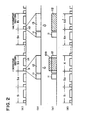
- a defective sector identification method in a pair art information recording and reproducing system is disclosed, for example, in Japanese Patent Application No. 60-49035 (1985). Further, a method for using an alternative sector for a defective sector is disclosed, for example, in Japanese Patent Laid-Open Publication No. 60-75931 (1985). The operation for using alternative sector for a defective sector in the information recording and reproducing system will be described with reference to Fig. 5. For example, it is supposed that defective sectors Xl and X2 exist among sectors Sl to S9 on a track T from which data is intended to be reproduced, and that it is recorded in a registor Rg beforehand that alternative sectors are a sector Sl' and a sector S2' on a track T'.
- the defective sector Xl located next to the sector S2 is skipped and the sector S4 is accessed. Further, the defective sector X2 located next to the sector S5 is skipped, and this sector S6 and the sectors following thereto are accessed.
- the track T' is sought to successively reproduce from the sectors Sl' and S2', and the reproduced data is sent to an area in a main memory to which otherwise reproduced data from the defective sectors X1 and X2 would be sent originally.
- An information recording and reproducing apparatus uses a disk type information recording and reproducing medium including within a same track a normal sector having an address formatted on an address area in a sector ID field, the address being capable of detecting an error, and including an alternative sector having no address formatted, and further, the apparatus is provided with address deleting means for disabling an address in a defective sector to be reproduced, and address recording means for recording an address in an address area in the alternative sector.
- a delete signal is recorded on the address area of the defective sector thereby to disable the address in the defective sector to be reproduced, next, an address which is the same as the defective sector is recorded in an address area in an unused alternative sector on the same track as the defective sector, and further, information to be recorded on the defective sector is recorded on the alternative sector.
- the alternative sector having the same address and data is formed on the same track as the defective sector, and thus, an information recording and reproducing apparatus is provided in which a high speed operation for using an alternative sector is made possible without requiring the use of a correspondence table between the defective sector and the alternative sector.
- Fig. 1 is a block diagram of an embodiment of an information recording and reproducing apparatus according to the present invention
- Fig. 2 is an operation outline explaining diagram for explaining an operation for using an alternative sector during data recording
- Fig. 3 is a flowchart for explaining a data recording operation
- Fig. 4 is a block diagram of address deleting means and address recording means which are actuated by using a timer
- Fig. 5 is an operation outline explaining diagram for explaining a prior art operation for using an alternative sector.
- Fig. 1 is a block diagram of an information recording and reproducing apparatus in an embodiment of the present invention.
- reference numeral 1 designates a main control circuit which controls the whole apparatus by receiving a device command from a host system (not shown).
- Reference numeral 2 designates a target sector detecting circuit which performs, after reading ID information such as a track address, a sector address, a CRCC code (cyclic redunduncy check code) for error checking, etc., from a reproducing signal 101 delivered from a drive unit 3 and after checking an error with respect to the CRCC, a coincidence detection with a target sector address 100 set by the main control circuit 1.
- ID information such as a track address, a sector address, a CRCC code (cyclic redunduncy check code) for error checking, etc.
- Reference numeral 5 designates a sector buffer for temporarily storing recording information 104 to be recorded on a target sector and reproduced information 14 reproduced from the target sector.
- Reference numeral 4 designates an information recording circuit which performs digital modulation of (2, 7) RLLC (run length limited code), etc., after coding the recording information 104 by adding thereto an error detection and correction code such as a reed solomon code, and delivers a produced recording signal 105 to a laser driving circuit (not shown) within the drive unit 3.
- Reference numeral 8 designates an information reproducing circuit which takes the reproducing signal 101 delivered from the drive unit 3 into a shift register, and produces the reproduced information 114 after demodulating an output of.the shift register by converting in a combining circuit and after decoding the demodulated output.
- Reference numeral 6 designates an address deleting circuit which supplies a delete signal 109 to the drive unit 3, and disables an address from a defective sector to be reproduced by recording the delete signal 109 on an address area in the defective sector by using the laser driving circuit within the drive unit 3.
- Reference numeral 7 designates an address recording circuit which performs digital modulation after adding the CRCC code for error checking to alternative address information 111, delivers the produced alternative address signal 112 to the drive unit 3, and records on the address area of the alternative sector by using the laser driving circuit within the drive unit 3.
- a method for modulating and demodulating the (2, 7) RLLC is disclosed in U.S. Patent No. 4,115,768 issued to Eggenber et al.
- the main control circuit 1 in order to detect a normal sector S2 which is located precedent to the defective sector S3, sends and sets an address of the normal sector S2 as the target sector address 100 to the target sector detecting circuit 2.
- the target sector detecting circuit 2 detects the normal sector S2 set by the main control circuit 1, delivers the detection signal 103 to the main control circuit 1, and the main control circuit 1 delivers a delete enable signal 107 to the address delete circuit 6.
- the drive unit 3 delivers a sector mark signal 108 after detecting the sector mark of the defective sector S3, the address delete circuit 6 is actuated and delivers the delete signal 109.
- the drive unit 3 overwrites the delete signal 109 on the address area 13 in the defective sector S3 as shown in Fig. 2, at (C) thereby to make the address of the defective sector S3 unable to be reproduced.
- the normal sector S3 is regarded as a defective sector having a defect in the address area.
- the delete signal 109 is overwritten on the address area 13 in the defective sector S3 thereby to make the address of the defective sector S3 completely unable to be reproduced.
- the main control circuit 1 in order to detect a normal sector Sn located precedent to the alternative sector Rl, sends and sets the address of the normal sector Sn to the target sector detecting circuit 2 as the target sector address 100.
- the target sector detecting circuit 2 detects the normal sector Sn set by the main control circuit 1
- the target sector detecting circuit 2 delivers the detection signal 103 to the main control circuit 1
- the main control circuit 1 delivers to the address recording circuit 7 the address write enable signal 110 and the alternative address information 111 containing the address of the defective sector S3.
- the drive unit 3 detects the sector mark of the alternative sector Rl and sends the sector mark signal 108, the address recording circuit 7 is actuated, and the address recording circuit 7 produces the alternative address signal 112 from the alternative address information 111 and delivers the alternative address signal 112 to the drive unit'3.
- the drive unit 3 records the alternative address signal 112 on the address area 13 in the alternative sector Rl as shown in Fig. 2, at (C), and by this recording, the same address as the defective sector S3 is recorded on the address area 13 in the alternative sector Rl which has been in an unrecorded condition.
- the disposition of the sectors on the target track is changed as shown in Fig. 2, at (D), and because of the fact that the address of the normal sector S3 is disabled to be reproduced, the normal sector S3 is identified as a defective sector X and also, the alternative sector Rl is identified as an alternative sector S3' which has the same address as the normal sector S3.
- the information which is to be recorded on the normal sector S3 is recorded alternatively on the alternative sector S3', and the operation for the alternative sector is completed.
- the delete signal 109 in the aforementioned procedure (G), when the address area of the information recording medium is formed with an irregular surface structure of the disk substrate as is the case in the write-once type optical disk, or when the rewriting of address information is impossible due to the properties of the recording material, it is possible to disable the address of the defective sector to be reproduced by using as the delete signal 109, for example, a signal having a pulse width wider than the signal contained in the signal 112 of the alternative address, and by overwriting the signal of the wider pulse width on the address area of the defective sector thereby to cause the CRCC error to be generated at the time of reproducing the address.
- the delete signal 109 for example, a signal having a pulse width wider than the signal contained in the signal 112 of the alternative address
- the information recording medium when used in which the rewriting of the address information is possible, it is possible to disable the address of the defective sector to be reproduced, for example, by using as the delete signal 109 a D.C. signal thereby to erase at least a portion of the address area.
- the main control circuit 1 delivers and sets as the target address 100 the address of the normal sector S3 to the target sector detecting circuit 2, and at the same time, delivers the read enable signal 113 to the information reproducing circuit 8.
- the target sector detecting circuit 2 detects address information contained in the reproducing signal 101 and performs coincidence detection with the target sector address 100.
- the target sector detecting circuit 2 detects, in place of the defective sector S3 whose address has been disabled to be reproduced, the alternative sector S3' having the same address recorded therein, the target sector detecting circuit 2 delivers the detection signal 103 to the information reproducing circuit 8.
- the information reproducing circuit 8 produces the reproduced information 114 from the reproducing signal 101 sent from the drive unit 3, and delivers to the sector buffer 5.
- the reproducing circuit 8 finishes the delivery of the reproduced information 114 the reproducing operation is completed when the reproduced information 114 which is stored temporarily in the sector buffer 5 is sent out to the host system.
- the number of the alternative sectors is not limited to this. Further, when a plurality of alternative sectors exist on the same track, the foregoing procedure for alternative sector can be executed also for the alternative sector which is regarded as a defective sector.
- the address deleting circuit 6 and the address recording circuit 7 are actuated by the sector mark signal 108 which is sent out when the drive unit 3 detects the sector mark 11.
- the sector mark 11 is not satisfactory or when the format recording has not been performed, the foregoing operation for alternative sector can not be executed.
- a method for actuating the address deleting circuit 6 or the address recording circuit 7 uses a timer for measuring a rotational latency corresponding to one sector in place of the sector mark signal 108. This method will be described with reference to a block diagram in Fig. 4. In Fig.
- the main control circuit 1 delivers measurement data 115 corresponding to a rotational latency corresponding to one sector to actuate a timer 15.
- the timer 15 measures a time corresponding to the measurement data 115 by counting a clock signal 116 delivered from an oscillator 16.
- the timer 15 sends an alternative actuation signal 117 to the address deleting circuit 6 or the address recording circuit 7.
- the address deleting circuit 6 or the address recording circuit 7 is actuated by the alternative actuation signal 117 in place ,.of the sector mark signal 108, and the operation for alternative sector can be executed.
- the information recording and reproducing apparatus in accordance with the present invention, when a defective sector is detected, first, the address of the defective sector is made impossible to be reproduced by recording a delete signal on the address area in the defective sector, then, the address of the defective sector is recorded on the address area in an alternative sector, and further, the information to be recorded on the defective sector is recorded within the alternative sector.
- the alternative sector having the same address and data as the defective sector is formed on the same track as the defective sector. Accordingly, at the time of reproduction, the access to the alternative sector becomes possible without a seek operation, and the processing speed is increased.
- the access to the alternative sector is enabled without using a correspondence table between the defective sector and the alternative sector, the structure of the apparatus can be made simple, and its practical effects are great.
- the information recording and reproducing apparatus uses an information recording medium including on the same track a normal sector having an address formatted on an address area within a sector ID field, and an alternative sector in which an address is not yet recorded.
- the apparatus when a defective sector is detected, first, the address of the defective sector is made impossible to be reproduced by recording a delete signal on the address area in the defective sector, then, the address of the defective sector is recorded on the address area in the alternative sector, and further the information to be recorded on the defective sector is recorded within the alternative sector.
- the alternative sector having the same address and data as the defective sector is formed on the same track as the defective sector. Accordingly, at the time of reproduction, the seek operation for accessing the alternative sector is not needed, and the processing speed is increased.
- the correspondence table between the defective sector and the alternative sector, etc. are not used, there is no need to provide a register and a buffer for administering the correspondence table, and the structure of the apparatus can be made simple.
Abstract
Description
- The present invention relates to an information recording and reproducing apparatus for recording and reproducing information on and from a disk type information recording medium having a plurality of sectors.
- With respect to information recording and reproducing systems for recording and reproducing information on and from a disk type information recording medium for each of sectors thereof, for example, in U.S. Patent No. 4,545,044, there is, disclosed an information recording and reproducing system which uses an optical disk.
- The optical disk is usually provided with a guide track which is detectable optically in order to form tracks with a higher density, and by irradiating a recording layer formed on the guide track with a laser light converged to about 1 um, a hole is formed or reflectivity is changed to effect the recording of the information.
- Since the recorded dot and the track pitch are about 1 µm, various defects are caused in a manufacturing process of the optical disk (formation of a guide track, manufacturing of a replica disk, evaporation of a recording material, formation of a protective film, and the like), or depending on an environment in which the disk is used. Due to such defects of the medium, sometimes a defective sector is detected in which a reproduction error occurs in an address or data. Further, in an information recording and reproducing system wherein rewriting is impossible due to the properties of a recording material as is the case in a write-once type optical disk, if the recording operation is interrupted during data recording, for example, due to a drive error, it results in the recording of incomplete data-in a sector, and it is regarded as a defective sector in file management.
- A defective sector identification method in a pair art information recording and reproducing system is disclosed, for example, in Japanese Patent Application No. 60-49035 (1985). Further, a method for using an alternative sector for a defective sector is disclosed, for example, in Japanese Patent Laid-Open Publication No. 60-75931 (1985). The operation for using alternative sector for a defective sector in the information recording and reproducing system will be described with reference to Fig. 5. For example, it is supposed that defective sectors Xl and X2 exist among sectors Sl to S9 on a track T from which data is intended to be reproduced, and that it is recorded in a registor Rg beforehand that alternative sectors are a sector Sl' and a sector S2' on a track T'. First, when the reproduction of the data is started with the sector Sl, the defective sector Xl located next to the sector S2 is skipped and the sector S4 is accessed. Further, the defective sector X2 located next to the sector S5 is skipped, and this sector S6 and the sectors following thereto are accessed. Next, the track T' is sought to successively reproduce from the sectors Sl' and S2', and the reproduced data is sent to an area in a main memory to which otherwise reproduced data from the defective sectors X1 and X2 would be sent originally.
- However, in the aforementioned system for using an alternative sector, it is necessary to provide within the system a register and a buffer to administer a correspondence table indicating a correspondence between a defective sector and an alternative sector, and to provide a table recording area in the information recording area every time a new defective sector is detected. Thus, overhead is increased both in hardware and software. Moreover, in the operation of replacing the defective sector with an alternative sector, a seek, operation is required to access the alternative sector existing on a specific track, and the data processing speed is decreased.
- An information recording and reproducing apparatus according to the present invention uses a disk type information recording and reproducing medium including within a same track a normal sector having an address formatted on an address area in a sector ID field, the address being capable of detecting an error, and including an alternative sector having no address formatted, and further, the apparatus is provided with address deleting means for disabling an address in a defective sector to be reproduced, and address recording means for recording an address in an address area in the alternative sector. In this apparatus, when the defective sector is detected, a delete signal is recorded on the address area of the defective sector thereby to disable the address in the defective sector to be reproduced, next, an address which is the same as the defective sector is recorded in an address area in an unused alternative sector on the same track as the defective sector, and further, information to be recorded on the defective sector is recorded on the alternative sector. In the present invention, owing to such an operation for using the alternative sector, the alternative sector having the same address and data is formed on the same track as the defective sector, and thus, an information recording and reproducing apparatus is provided in which a high speed operation for using an alternative sector is made possible without requiring the use of a correspondence table between the defective sector and the alternative sector.
- Fig. 1 is a block diagram of an embodiment of an information recording and reproducing apparatus according to the present invention, Fig. 2 is an operation outline explaining diagram for explaining an operation for using an alternative sector during data recording, Fig. 3 is a flowchart for explaining a data recording operation, Fig. 4 is a block diagram of address deleting means and address recording means which are actuated by using a timer, and Fig. 5 is an operation outline explaining diagram for explaining a prior art operation for using an alternative sector.
- Fig. 1 is a block diagram of an information recording and reproducing apparatus in an embodiment of the present invention. In Fig. 1, reference numeral 1 designates a main control circuit which controls the whole apparatus by receiving a device command from a host system (not shown).
Reference numeral 2 designates a target sector detecting circuit which performs, after reading ID information such as a track address, a sector address, a CRCC code (cyclic redunduncy check code) for error checking, etc., from a reproducingsignal 101 delivered from adrive unit 3 and after checking an error with respect to the CRCC, a coincidence detection with atarget sector address 100 set by the main control circuit 1.Reference numeral 5 designates a sector buffer for temporarily storingrecording information 104 to be recorded on a target sector and reproducedinformation 14 reproduced from the target sector. Reference numeral 4 designates an information recording circuit which performs digital modulation of (2, 7) RLLC (run length limited code), etc., after coding therecording information 104 by adding thereto an error detection and correction code such as a reed solomon code, and delivers a producedrecording signal 105 to a laser driving circuit (not shown) within thedrive unit 3.Reference numeral 8 designates an information reproducing circuit which takes the reproducingsignal 101 delivered from thedrive unit 3 into a shift register, and produces the reproducedinformation 114 after demodulating an output of.the shift register by converting in a combining circuit and after decoding the demodulated output.Reference numeral 6 designates an address deleting circuit which supplies adelete signal 109 to thedrive unit 3, and disables an address from a defective sector to be reproduced by recording thedelete signal 109 on an address area in the defective sector by using the laser driving circuit within thedrive unit 3.Reference numeral 7 designates an address recording circuit which performs digital modulation after adding the CRCC code for error checking to alternative address information 111, delivers the producedalternative address signal 112 to thedrive unit 3, and records on the address area of the alternative sector by using the laser driving circuit within thedrive unit 3. In this respect, a method for modulating and demodulating the (2, 7) RLLC is disclosed in U.S. Patent No. 4,115,768 issued to Eggenber et al. - The operation of the information recording and reproducing apparatus in the embodiment arranged as described in the foregoing will be described with reference to an operation outline explaining diagram in Fig. 2 and a flowchart in Fig. 3. In this embodiment, an information recording medium wherein the rewriting is impossible as in a write-once type optical disk is used, and a seek operation is omitted in order to simplify the explanation. Further, it is supposed that a head has already been existing on a target track. On the target track, as shown in Fig. 2, at (a), there are existing normal sectors Sl to Sn and a first alternative sector Rl. In a
sector ID field 9 in each of the normal sectors, and in asector ID field 10 in the alternative sector, similarly in both cases as shown in Fig. 2, at (b), there are recorded withsector marks 11 in a format at the beginning of each of the sector ID fields. Further, although an address having an error detecting capability is recorded in a format on anaddress area 12 in each of the normal sectors, no recording is made on anaddress area 13 in the alternative sector. The operation described in the flowchart in Fig. 3 indicates that when a drive error occurs during data recording operation on adata field 14 in the normal sector S3, the data recording operation will be interrupted and incomplete data will be recorded in the normal sector S3. Since, rewriting in the normal sector S3 is impossible, the normal sector S3 is regarded as a defective sector, and the information which is to be recorded at this time is recorded alternatively on the unused alternative sector Rl. - (A) The main control circuit 1 delivers and sets the
target sector address 100 to the targetsector detecting circuit 2, and at the same time, delivers the write enablesignal 102 to the information recording circuit 4. - (B) The target
sector detecting circuit 2 detects address information contained in the reproducingsignal 101, and performs coincidence detection with thetarget sector address 100 set by the main control circuit 1. - (C) When the target sector S3 is detected in the operation in (B), the target
sector detecting circuit 2 delivers thedetection signal 103 to the information recording circuit 4. The information recording circuit 4 produces therecording signal 105 from therecording information 104 which has been supplied from the host system and stored temporarily in thesector buffer 5, and starts recording of data by delivering the producedrecording signal 105 to thedrive unit 3. - (D) During the data recording operation, the
drive unit 3 performs detection of a drive error. - (E) The recording operation of data is finished by completing the sending of the
recording signal 105 to the target sector S3 by the information recording circuit 4. - (F) When the drive error is detected in the operation in (D), the main control circuit 1 detects as an interrupt signal the
drive error signal 106 delivered from thedrive unit 3, and stops sending of the write enablesignal 102. As a result, the information recording circuit 4 stops sending of therecording signal 105, and the data recording operation is interrupted. - (G) When the data recording operation is interrupted, since the information recording medium is unable to be rewritten, the normal sector S3 in which incomplete data has been recorded is regarded as a defective sector.
- The main control circuit 1, in order to detect a normal sector S2 which is located precedent to the defective sector S3, sends and sets an address of the normal sector S2 as the
target sector address 100 to the targetsector detecting circuit 2. When the targetsector detecting circuit 2 detects the normal sector S2 set by the main control circuit 1, delivers thedetection signal 103 to the main control circuit 1, and the main control circuit 1 delivers a delete enablesignal 107 to the address deletecircuit 6. When thedrive unit 3 delivers asector mark signal 108 after detecting the sector mark of the defective sector S3, theaddress delete circuit 6 is actuated and delivers thedelete signal 109. Thedrive unit 3 overwrites thedelete signal 109 on theaddress area 13 in the defective sector S3 as shown in Fig. 2, at (C) thereby to make the address of the defective sector S3 unable to be reproduced. - Further, in the operation in (B), when the target sector can not be detected within a maximum rotational latency (that is, when there is a defect in the address area in the target sector, etc.), the normal sector S3 is regarded as a defective sector having a defect in the address area. In order to prevent erroneous detection of the target sector thereafter due to unsatisfactory address reproduction, in accordance with a procedure similar to that described above, the
delete signal 109 is overwritten on theaddress area 13 in the defective sector S3 thereby to make the address of the defective sector S3 completely unable to be reproduced. - (H) The main control circuit 1, in order to detect a normal sector Sn located precedent to the alternative sector Rl, sends and sets the address of the normal sector Sn to the target
sector detecting circuit 2 as thetarget sector address 100. When the targetsector detecting circuit 2 detects the normal sector Sn set by the main control circuit 1, the targetsector detecting circuit 2 delivers thedetection signal 103 to the main control circuit 1, and the main control circuit 1 delivers to theaddress recording circuit 7 the address write enablesignal 110 and the alternative address information 111 containing the address of the defective sector S3. Then, when thedrive unit 3 detects the sector mark of the alternative sector Rl and sends thesector mark signal 108, theaddress recording circuit 7 is actuated, and theaddress recording circuit 7 produces thealternative address signal 112 from the alternative address information 111 and delivers thealternative address signal 112 to the drive unit'3. Thedrive unit 3 records thealternative address signal 112 on theaddress area 13 in the alternative sector Rl as shown in Fig. 2, at (C), and by this recording, the same address as the defective sector S3 is recorded on theaddress area 13 in the alternative sector Rl which has been in an unrecorded condition. - By the procedure as described above, the disposition of the sectors on the target track is changed as shown in Fig. 2, at (D), and because of the fact that the address of the normal sector S3 is disabled to be reproduced, the normal sector S3 is identified as a defective sector X and also, the alternative sector Rl is identified as an alternative sector S3' which has the same address as the normal sector S3. Thus, the information which is to be recorded on the normal sector S3 is recorded alternatively on the alternative sector S3', and the operation for the alternative sector is completed.
- Further, in the recording of the
delete signal 109 in the aforementioned procedure (G), when the address area of the information recording medium is formed with an irregular surface structure of the disk substrate as is the case in the write-once type optical disk, or when the rewriting of address information is impossible due to the properties of the recording material, it is possible to disable the address of the defective sector to be reproduced by using as thedelete signal 109, for example, a signal having a pulse width wider than the signal contained in thesignal 112 of the alternative address, and by overwriting the signal of the wider pulse width on the address area of the defective sector thereby to cause the CRCC error to be generated at the time of reproducing the address. Further, when the information recording medium is used in which the rewriting of the address information is possible, it is possible to disable the address of the defective sector to be reproduced, for example, by using as the delete signal 109 a D.C. signal thereby to erase at least a portion of the address area. - Next, in this embodiment, the reproducing operation of information recorded alternatively on the alternative sector S3' will be described with reference to the block diagram in Fig. 1.
- First, the main control circuit 1 delivers and sets as the
target address 100 the address of the normal sector S3 to the targetsector detecting circuit 2, and at the same time, delivers the read enablesignal 113 to theinformation reproducing circuit 8. The targetsector detecting circuit 2 detects address information contained in the reproducingsignal 101 and performs coincidence detection with thetarget sector address 100. When the targetsector detecting circuit 2 detects, in place of the defective sector S3 whose address has been disabled to be reproduced, the alternative sector S3' having the same address recorded therein, the targetsector detecting circuit 2 delivers thedetection signal 103 to theinformation reproducing circuit 8. Theinformation reproducing circuit 8. Theinformation reproducing circuit 8 produces the reproducedinformation 114 from the reproducingsignal 101 sent from thedrive unit 3, and delivers to thesector buffer 5. When theinformation reproducing circuit 8 finishes the delivery of the reproducedinformation 114, the reproducing operation is completed when the reproducedinformation 114 which is stored temporarily in thesector buffer 5 is sent out to the host system. - In the above embodiment, although one alternative sector exists on the target track, the number of the alternative sectors is not limited to this. Further, when a plurality of alternative sectors exist on the same track, the foregoing procedure for alternative sector can be executed also for the alternative sector which is regarded as a defective sector.
- Further, in the above embodiment, the
address deleting circuit 6 and theaddress recording circuit 7 are actuated by the sector mark signal 108 which is sent out when thedrive unit 3 detects thesector mark 11. However, when thesector mark 11 is not satisfactory or when the format recording has not been performed, the foregoing operation for alternative sector can not be executed. In such a case, a method for actuating theaddress deleting circuit 6 or theaddress recording circuit 7 uses a timer for measuring a rotational latency corresponding to one sector in place of thesector mark signal 108. This method will be described with reference to a block diagram in Fig. 4. In Fig. 4, when a sector existing precedent to the defective sector or the alternative sector is detected, the main control circuit 1 deliversmeasurement data 115 corresponding to a rotational latency corresponding to one sector to actuate atimer 15. Thetimer 15 measures a time corresponding to themeasurement data 115 by counting a clock signal 116 delivered from anoscillator 16. At the time point at which the measurement of the rotational latency corresponding to one sector is finished, thetimer 15 sends analternative actuation signal 117 to theaddress deleting circuit 6 or theaddress recording circuit 7. By such a procedure, theaddress deleting circuit 6 or theaddress recording circuit 7 is actuated by thealternative actuation signal 117 in place ,.of thesector mark signal 108, and the operation for alternative sector can be executed.. - As described in the foregoing, in the information recording and reproducing apparatus in accordance with the present invention, when a defective sector is detected, first, the address of the defective sector is made impossible to be reproduced by recording a delete signal on the address area in the defective sector, then, the address of the defective sector is recorded on the address area in an alternative sector, and further, the information to be recorded on the defective sector is recorded within the alternative sector. By such an operation for alternative sector, the alternative sector having the same address and data as the defective sector is formed on the same track as the defective sector. Accordingly, at the time of reproduction, the access to the alternative sector becomes possible without a seek operation, and the processing speed is increased. Moreover, since the access to the alternative sector is enabled without using a correspondence table between the defective sector and the alternative sector, the structure of the apparatus can be made simple, and its practical effects are great.
- The information recording and reproducing apparatus according to the present invention uses an information recording medium including on the same track a normal sector having an address formatted on an address area within a sector ID field, and an alternative sector in which an address is not yet recorded. In the apparatus, when a defective sector is detected, first, the address of the defective sector is made impossible to be reproduced by recording a delete signal on the address area in the defective sector, then, the address of the defective sector is recorded on the address area in the alternative sector, and further the information to be recorded on the defective sector is recorded within the alternative sector. As a result, the alternative sector having the same address and data as the defective sector is formed on the same track as the defective sector. Accordingly, at the time of reproduction, the seek operation for accessing the alternative sector is not needed, and the processing speed is increased. Moreover, since the correspondence table between the defective sector and the alternative sector, etc., are not used, there is no need to provide a register and a buffer for administering the correspondence table, and the structure of the apparatus can be made simple.
Claims (5)
Applications Claiming Priority (2)
| Application Number | Priority Date | Filing Date | Title |
|---|---|---|---|
| JP60241060A JPS62102482A (en) | 1985-10-28 | 1985-10-28 | Information recording and reproducing device |
| JP241060/85 | 1985-10-28 |
Publications (3)
| Publication Number | Publication Date |
|---|---|
| EP0243503A1 true EP0243503A1 (en) | 1987-11-04 |
| EP0243503A4 EP0243503A4 (en) | 1988-03-03 |
| EP0243503B1 EP0243503B1 (en) | 1990-07-18 |
Family
ID=17068707
Family Applications (1)
| Application Number | Title | Priority Date | Filing Date |
|---|---|---|---|
| EP86906442A Expired EP0243503B1 (en) | 1985-10-28 | 1986-10-27 | Data recording/regenerating device |
Country Status (5)
| Country | Link |
|---|---|
| US (2) | US4885735A (en) |
| EP (1) | EP0243503B1 (en) |
| JP (1) | JPS62102482A (en) |
| DE (1) | DE3672828D1 (en) |
| WO (1) | WO1987002818A1 (en) |
Cited By (34)
| Publication number | Priority date | Publication date | Assignee | Title |
|---|---|---|---|---|
| EP0617363A2 (en) * | 1989-04-13 | 1994-09-28 | Sundisk Corporation | Defective cell substitution in EEprom array |
| EP0623927A1 (en) * | 1993-04-30 | 1994-11-09 | Nec Corporation | Magnetic disk apparatus |
| US5535328A (en) * | 1989-04-13 | 1996-07-09 | Sandisk Corporation | Non-volatile memory system card with flash erasable sectors of EEprom cells including a mechanism for substituting defective cells |
| US5838614A (en) * | 1995-07-31 | 1998-11-17 | Lexar Microsystems, Inc. | Identification and verification of a sector within a block of mass storage flash memory |
| US5907856A (en) * | 1995-07-31 | 1999-05-25 | Lexar Media, Inc. | Moving sectors within a block of information in a flash memory mass storage architecture |
| US5928370A (en) * | 1997-02-05 | 1999-07-27 | Lexar Media, Inc. | Method and apparatus for verifying erasure of memory blocks within a non-volatile memory structure |
| US5930815A (en) * | 1995-07-31 | 1999-07-27 | Lexar Media, Inc. | Moving sequential sectors within a block of information in a flash memory mass storage architecture |
| US6034897A (en) * | 1999-04-01 | 2000-03-07 | Lexar Media, Inc. | Space management for managing high capacity nonvolatile memory |
| US6076137A (en) * | 1997-12-11 | 2000-06-13 | Lexar Media, Inc. | Method and apparatus for storing location identification information within non-volatile memory devices |
| US6081878A (en) * | 1997-03-31 | 2000-06-27 | Lexar Media, Inc. | Increasing the memory performance of flash memory devices by writing sectors simultaneously to multiple flash memory devices |
| US6115785A (en) * | 1995-07-31 | 2000-09-05 | Lexar Media, Inc. | Direct logical block addressing flash memory mass storage architecture |
| US6122195A (en) * | 1997-03-31 | 2000-09-19 | Lexar Media, Inc. | Method and apparatus for decreasing block write operation times performed on nonvolatile memory |
| US6125435A (en) * | 1995-09-13 | 2000-09-26 | Lexar Media, Inc. | Alignment of cluster address to block addresses within a semiconductor non-volatile mass storage memory |
| US6141249A (en) * | 1999-04-01 | 2000-10-31 | Lexar Media, Inc. | Organization of blocks within a nonvolatile memory unit to effectively decrease sector write operation time |
| US6262918B1 (en) | 1999-04-01 | 2001-07-17 | Lexar Media, Inc. | Space management for managing high capacity nonvolatile memory |
| EP0702370B1 (en) * | 1994-09-05 | 2001-07-25 | Sony Corporation | Data reproduction |
| US6374337B1 (en) | 1998-11-17 | 2002-04-16 | Lexar Media, Inc. | Data pipelining method and apparatus for memory control circuit |
| US6411546B1 (en) | 1997-03-31 | 2002-06-25 | Lexar Media, Inc. | Nonvolatile memory using flexible erasing methods and method and system for using same |
| US6567307B1 (en) | 2000-07-21 | 2003-05-20 | Lexar Media, Inc. | Block management for mass storage |
| US6728851B1 (en) | 1995-07-31 | 2004-04-27 | Lexar Media, Inc. | Increasing the memory performance of flash memory devices by writing sectors simultaneously to multiple flash memory devices |
| US6757800B1 (en) | 1995-07-31 | 2004-06-29 | Lexar Media, Inc. | Increasing the memory performance of flash memory devices by writing sectors simultaneously to multiple flash memory devices |
| US6801979B1 (en) | 1995-07-31 | 2004-10-05 | Lexar Media, Inc. | Method and apparatus for memory control circuit |
| US6813678B1 (en) | 1998-01-22 | 2004-11-02 | Lexar Media, Inc. | Flash memory system |
| US6898662B2 (en) | 2001-09-28 | 2005-05-24 | Lexar Media, Inc. | Memory system sectors |
| US7190617B1 (en) | 1989-04-13 | 2007-03-13 | Sandisk Corporation | Flash EEprom system |
| US7725628B1 (en) | 2004-04-20 | 2010-05-25 | Lexar Media, Inc. | Direct secondary device interface by a host |
| US7743290B2 (en) | 2004-08-27 | 2010-06-22 | Lexar Media, Inc. | Status of overall health of nonvolatile memory |
| US7865659B2 (en) | 2004-04-30 | 2011-01-04 | Micron Technology, Inc. | Removable storage device |
| US7908426B2 (en) | 1995-07-31 | 2011-03-15 | Lexar Media, Inc. | Moving sectors within a block of information in a flash memory mass storage architecture |
| US7917709B2 (en) | 2001-09-28 | 2011-03-29 | Lexar Media, Inc. | Memory system for data storage and retrieval |
| US7944762B2 (en) | 2001-09-28 | 2011-05-17 | Micron Technology, Inc. | Non-volatile memory control |
| US7949822B2 (en) | 2004-08-27 | 2011-05-24 | Micron Technology, Inc. | Storage capacity status |
| US8171203B2 (en) | 1995-07-31 | 2012-05-01 | Micron Technology, Inc. | Faster write operations to nonvolatile memory using FSInfo sector manipulation |
| US8386695B2 (en) | 2001-09-28 | 2013-02-26 | Micron Technology, Inc. | Methods and apparatus for writing data to non-volatile memory |
Families Citing this family (28)
| Publication number | Priority date | Publication date | Assignee | Title |
|---|---|---|---|---|
| JPH0673226B2 (en) * | 1987-06-12 | 1994-09-14 | 株式会社シーエスケイ | Optical recording medium read error detection device |
| US5268319A (en) | 1988-06-08 | 1993-12-07 | Eliyahou Harari | Highly compact EPROM and flash EEPROM devices |
| JPH031370A (en) * | 1989-05-29 | 1991-01-08 | Nec Corp | Write / read control circuit for magnetic disk device |
| CA2020059C (en) * | 1989-06-30 | 1995-05-23 | Shigemi Maeda | Modular ceramic igniter |
| JP3057498B2 (en) * | 1989-08-02 | 2000-06-26 | 富士通株式会社 | Array disk device and data reading method thereof |
| JPH03116583A (en) * | 1989-09-29 | 1991-05-17 | Toshiba Corp | Optical disk device |
| US5737632A (en) * | 1989-12-19 | 1998-04-07 | Hitachi, Ltd. | Magnetic disc control apparatus with parallel data transfer between disc control unit and encoder/decoder circuit |
| JP3373218B2 (en) * | 1991-12-26 | 2003-02-04 | パイオニア株式会社 | Recording / reproducing method for writable disk drive device |
| JPH05324489A (en) * | 1992-05-15 | 1993-12-07 | Toshiba Corp | Storage device |
| JP3225640B2 (en) * | 1992-10-23 | 2001-11-05 | ソニー株式会社 | Recording device |
| US5422761A (en) * | 1992-11-20 | 1995-06-06 | International Business Machines Corporation | Disk drive with redundant recording |
| EP0640924A3 (en) * | 1993-08-17 | 1997-04-23 | Sony Corp | Data reproducing apparatus. |
| US5818654A (en) * | 1994-06-13 | 1998-10-06 | Seagate Technology, Inc. | Apparatus and process for managing defective headerless sectors |
| US5983309A (en) * | 1994-07-27 | 1999-11-09 | Seagate Technology, Inc. | Autonomous high speed address translation with defect management for hard disc drives |
| JP3029399B2 (en) * | 1996-03-25 | 2000-04-04 | 株式会社東芝 | Replacement processing method |
| JP3113200B2 (en) * | 1996-03-25 | 2000-11-27 | 株式会社東芝 | Replacement processing method |
| JP2848809B2 (en) * | 1996-03-25 | 1999-01-20 | 株式会社東芝 | Replacement processing method |
| JP3113201B2 (en) * | 1996-03-25 | 2000-11-27 | 株式会社東芝 | Replacement processing method |
| JP3029400B2 (en) * | 1996-03-25 | 2000-04-04 | 株式会社東芝 | Replacement processing method |
| JPH10312650A (en) * | 1997-05-14 | 1998-11-24 | Ricoh Co Ltd | Optical disk recorder |
| JPH11232791A (en) * | 1998-02-10 | 1999-08-27 | Sony Corp | Information recording method and device therefor |
| JP4324276B2 (en) * | 1998-06-03 | 2009-09-02 | 株式会社日立グローバルストレージテクノロジーズ | Magnetic disk error correction method and apparatus |
| US6754680B1 (en) * | 1999-05-20 | 2004-06-22 | Matsushita Electric Industrial Co., Ltd. | Data control equipment, method to control data and recording medium to record data control procedure |
| US7167944B1 (en) | 2000-07-21 | 2007-01-23 | Lexar Media, Inc. | Block management for mass storage |
| GB0123421D0 (en) | 2001-09-28 | 2001-11-21 | Memquest Ltd | Power management system |
| US7231643B1 (en) | 2002-02-22 | 2007-06-12 | Lexar Media, Inc. | Image rescue system including direct communication between an application program and a device driver |
| JP2006113833A (en) * | 2004-10-15 | 2006-04-27 | Hitachi Ltd | Storage management device, storage network system, storage management method and program |
| JP5955092B2 (en) * | 2011-10-12 | 2016-07-20 | パナソニックIpマネジメント株式会社 | Optical recording / reproducing apparatus and reproducing apparatus |
Citations (5)
| Publication number | Priority date | Publication date | Assignee | Title |
|---|---|---|---|---|
| JPS58203685A (en) * | 1982-05-20 | 1983-11-28 | Hitachi Medical Corp | Magnetic disk controller |
| JPS59113509A (en) * | 1982-12-20 | 1984-06-30 | Nec Corp | Disc processing device |
| EP0127311A2 (en) * | 1983-05-23 | 1984-12-05 | Data General Corporation | Method of and controller for handling medium defects in a disc drive system |
| WO1985001380A1 (en) * | 1983-09-19 | 1985-03-28 | Storage Technology Partners Ii | Optical disk format employing resynchronizable data sectors |
| EP0194640A2 (en) * | 1985-03-12 | 1986-09-17 | Matsushita Electric Industrial Co., Ltd. | Information recording and reproducing apparatus |
Family Cites Families (12)
| Publication number | Priority date | Publication date | Assignee | Title |
|---|---|---|---|---|
| DE2508706C2 (en) * | 1974-05-02 | 1984-10-11 | International Business Machines Corp., Armonk, N.Y. | Circuit arrangement for coding data bit sequences |
| FR2426938A1 (en) * | 1978-05-26 | 1979-12-21 | Cii Honeywell Bull | DEVICE FOR DETECTION OF DEFECTIVE SECTORS AND ALLOCATION OF REPLACEMENT SECTORS IN A DISK MEMORY |
| US4259475A (en) * | 1979-03-29 | 1981-03-31 | Exxon Research & Engineering Co. | Preparation of linear crystalline homopolybenzyl |
| JPS5641515A (en) * | 1979-09-12 | 1981-04-18 | Nec Corp | Retry system of magnetic tape memory device |
| JPS5755580A (en) * | 1980-09-20 | 1982-04-02 | Sanyo Electric Co Ltd | Address writing-in method of magnetic disk |
| JPS5832236A (en) * | 1981-08-18 | 1983-02-25 | Matsushita Electric Ind Co Ltd | Optical recorder and reproducer |
| JPS5835733A (en) * | 1981-08-26 | 1983-03-02 | Fujitsu Ltd | Information recording and reproducing system |
| JPS59188814A (en) * | 1983-04-12 | 1984-10-26 | Nec Corp | Medium recording system |
| JPS60179980A (en) * | 1984-02-25 | 1985-09-13 | Canon Inc | Information recording method |
| US4695993A (en) * | 1984-06-15 | 1987-09-22 | Matsushita Electric Industrial Co., Ltd. | Optical information recording and reproducing apparatus and optical disc |
| JP2549241B2 (en) * | 1992-05-22 | 1996-10-30 | インターナショナル・ビジネス・マシーンズ・コーポレイション | Computer system |
| JP3199473B2 (en) * | 1992-08-12 | 2001-08-20 | 株式会社小松製作所 | Resistance diffusion bonding method |
-
1985
- 1985-10-28 JP JP60241060A patent/JPS62102482A/en active Pending
-
1986
- 1986-10-27 EP EP86906442A patent/EP0243503B1/en not_active Expired
- 1986-10-27 DE DE8686906442T patent/DE3672828D1/en not_active Expired - Lifetime
- 1986-10-27 US US07/076,170 patent/US4885735A/en not_active Expired - Fee Related
- 1986-10-27 WO PCT/JP1986/000539 patent/WO1987002818A1/en active IP Right Grant
-
1989
- 1989-10-03 US US07/416,834 patent/US4986668A/en not_active Expired - Fee Related
Patent Citations (5)
| Publication number | Priority date | Publication date | Assignee | Title |
|---|---|---|---|---|
| JPS58203685A (en) * | 1982-05-20 | 1983-11-28 | Hitachi Medical Corp | Magnetic disk controller |
| JPS59113509A (en) * | 1982-12-20 | 1984-06-30 | Nec Corp | Disc processing device |
| EP0127311A2 (en) * | 1983-05-23 | 1984-12-05 | Data General Corporation | Method of and controller for handling medium defects in a disc drive system |
| WO1985001380A1 (en) * | 1983-09-19 | 1985-03-28 | Storage Technology Partners Ii | Optical disk format employing resynchronizable data sectors |
| EP0194640A2 (en) * | 1985-03-12 | 1986-09-17 | Matsushita Electric Industrial Co., Ltd. | Information recording and reproducing apparatus |
Non-Patent Citations (3)
| Title |
|---|
| PATENT ABSTRACTS OF JAPAN, vol. 8, no. 237 (P-310)[1674], 30th October 1984; & JP-A-59 113 509 (NIPPON DENKI K.K.) 30-06-1984 * |
| PATENT ABSTRACTS OF JAPAN, vol. 8, no. 55 (P-260)[1492], 13th March 1984; & JP-A-58 203 685 (HITACHI MEDEIKO K.K.) 28-11-1983 * |
| See also references of WO8702818A1 * |
Cited By (72)
| Publication number | Priority date | Publication date | Assignee | Title |
|---|---|---|---|---|
| US5877986A (en) * | 1989-04-13 | 1999-03-02 | Sandisk Corporation | Multi-state Flash EEprom system on a card that includes defective cell substitution |
| US5671229A (en) * | 1989-04-13 | 1997-09-23 | Sandisk Corporation | Flash eeprom system with defect handling |
| EP0617363A3 (en) * | 1989-04-13 | 1995-03-08 | Sundisk Corp | Defective cell substitution in EEprom array. |
| EP0617363A2 (en) * | 1989-04-13 | 1994-09-28 | Sundisk Corporation | Defective cell substitution in EEprom array |
| US5535328A (en) * | 1989-04-13 | 1996-07-09 | Sandisk Corporation | Non-volatile memory system card with flash erasable sectors of EEprom cells including a mechanism for substituting defective cells |
| US5602987A (en) * | 1989-04-13 | 1997-02-11 | Sandisk Corporation | Flash EEprom system |
| US6373747B1 (en) | 1989-04-13 | 2002-04-16 | Sandisk Corporation | Flash EEprom system |
| EP1031992A3 (en) * | 1989-04-13 | 2003-08-13 | SanDisk Corporation | Flash EEPROM system |
| US7190617B1 (en) | 1989-04-13 | 2007-03-13 | Sandisk Corporation | Flash EEprom system |
| EP1031992A2 (en) * | 1989-04-13 | 2000-08-30 | SanDisk Corporation | Flash EEPROM system |
| US5862080A (en) * | 1989-04-13 | 1999-01-19 | Sandisk Corporation | Multi-state flash EEprom system with defect handling |
| US7492660B2 (en) | 1989-04-13 | 2009-02-17 | Sandisk Corporation | Flash EEprom system |
| EP0623927A1 (en) * | 1993-04-30 | 1994-11-09 | Nec Corporation | Magnetic disk apparatus |
| US5450251A (en) * | 1993-04-30 | 1995-09-12 | Nec Corporation | Sector relocation system in a magnetic disc apparatus |
| EP0702370B1 (en) * | 1994-09-05 | 2001-07-25 | Sony Corporation | Data reproduction |
| US6223308B1 (en) | 1995-07-31 | 2001-04-24 | Lexar Media, Inc. | Identification and verification of a sector within a block of mass STO rage flash memory |
| US6115785A (en) * | 1995-07-31 | 2000-09-05 | Lexar Media, Inc. | Direct logical block addressing flash memory mass storage architecture |
| US7908426B2 (en) | 1995-07-31 | 2011-03-15 | Lexar Media, Inc. | Moving sectors within a block of information in a flash memory mass storage architecture |
| US8171203B2 (en) | 1995-07-31 | 2012-05-01 | Micron Technology, Inc. | Faster write operations to nonvolatile memory using FSInfo sector manipulation |
| US8793430B2 (en) | 1995-07-31 | 2014-07-29 | Micron Technology, Inc. | Electronic system having memory with a physical block having a sector storing data and indicating a move status of another sector of the physical block |
| US6128695A (en) * | 1995-07-31 | 2000-10-03 | Lexar Media, Inc. | Identification and verification of a sector within a block of mass storage flash memory |
| US8078797B2 (en) | 1995-07-31 | 2011-12-13 | Micron Technology, Inc. | Increasing the memory performance of flash memory devices by writing sectors simultaneously to multiple flash memory devices |
| US8032694B2 (en) | 1995-07-31 | 2011-10-04 | Micron Technology, Inc. | Direct logical block addressing flash memory mass storage architecture |
| US6757800B1 (en) | 1995-07-31 | 2004-06-29 | Lexar Media, Inc. | Increasing the memory performance of flash memory devices by writing sectors simultaneously to multiple flash memory devices |
| US6172906B1 (en) | 1995-07-31 | 2001-01-09 | Lexar Media, Inc. | Increasing the memory performance of flash memory devices by writing sectors simultaneously to multiple flash memory devices |
| US6728851B1 (en) | 1995-07-31 | 2004-04-27 | Lexar Media, Inc. | Increasing the memory performance of flash memory devices by writing sectors simultaneously to multiple flash memory devices |
| US8554985B2 (en) | 1995-07-31 | 2013-10-08 | Micron Technology, Inc. | Memory block identified by group of logical block addresses, storage device with movable sectors, and methods |
| US6145051A (en) * | 1995-07-31 | 2000-11-07 | Lexar Media, Inc. | Moving sectors within a block of information in a flash memory mass storage architecture |
| US7774576B2 (en) | 1995-07-31 | 2010-08-10 | Lexar Media, Inc. | Direct logical block addressing flash memory mass storage architecture |
| US5930815A (en) * | 1995-07-31 | 1999-07-27 | Lexar Media, Inc. | Moving sequential sectors within a block of information in a flash memory mass storage architecture |
| US9026721B2 (en) | 1995-07-31 | 2015-05-05 | Micron Technology, Inc. | Managing defective areas of memory |
| US6393513B2 (en) | 1995-07-31 | 2002-05-21 | Lexar Media, Inc. | Identification and verification of a sector within a block of mass storage flash memory |
| US5907856A (en) * | 1995-07-31 | 1999-05-25 | Lexar Media, Inc. | Moving sectors within a block of information in a flash memory mass storage architecture |
| US6912618B2 (en) | 1995-07-31 | 2005-06-28 | Lexar Media, Inc. | Direct logical block addressing flash memory mass storage architecture |
| US6801979B1 (en) | 1995-07-31 | 2004-10-05 | Lexar Media, Inc. | Method and apparatus for memory control circuit |
| US5838614A (en) * | 1995-07-31 | 1998-11-17 | Lexar Microsystems, Inc. | Identification and verification of a sector within a block of mass storage flash memory |
| US8397019B2 (en) | 1995-07-31 | 2013-03-12 | Micron Technology, Inc. | Memory for accessing multiple sectors of information substantially concurrently |
| US6125435A (en) * | 1995-09-13 | 2000-09-26 | Lexar Media, Inc. | Alignment of cluster address to block addresses within a semiconductor non-volatile mass storage memory |
| US5928370A (en) * | 1997-02-05 | 1999-07-27 | Lexar Media, Inc. | Method and apparatus for verifying erasure of memory blocks within a non-volatile memory structure |
| US6587382B1 (en) | 1997-03-31 | 2003-07-01 | Lexar Media, Inc. | Nonvolatile memory using flexible erasing methods and method and system for using same |
| US6081878A (en) * | 1997-03-31 | 2000-06-27 | Lexar Media, Inc. | Increasing the memory performance of flash memory devices by writing sectors simultaneously to multiple flash memory devices |
| US6122195A (en) * | 1997-03-31 | 2000-09-19 | Lexar Media, Inc. | Method and apparatus for decreasing block write operation times performed on nonvolatile memory |
| US6411546B1 (en) | 1997-03-31 | 2002-06-25 | Lexar Media, Inc. | Nonvolatile memory using flexible erasing methods and method and system for using same |
| US6327639B1 (en) | 1997-12-11 | 2001-12-04 | Lexar Media, Inc. | Method and apparatus for storing location identification information within non-volatile memory devices |
| US6076137A (en) * | 1997-12-11 | 2000-06-13 | Lexar Media, Inc. | Method and apparatus for storing location identification information within non-volatile memory devices |
| US6813678B1 (en) | 1998-01-22 | 2004-11-02 | Lexar Media, Inc. | Flash memory system |
| US6374337B1 (en) | 1998-11-17 | 2002-04-16 | Lexar Media, Inc. | Data pipelining method and apparatus for memory control circuit |
| US6141249A (en) * | 1999-04-01 | 2000-10-31 | Lexar Media, Inc. | Organization of blocks within a nonvolatile memory unit to effectively decrease sector write operation time |
| US6034897A (en) * | 1999-04-01 | 2000-03-07 | Lexar Media, Inc. | Space management for managing high capacity nonvolatile memory |
| US6262918B1 (en) | 1999-04-01 | 2001-07-17 | Lexar Media, Inc. | Space management for managing high capacity nonvolatile memory |
| US6134151A (en) * | 1999-04-01 | 2000-10-17 | Lexar Media, Inc. | Space management for managing high capacity nonvolatile memory |
| US6567307B1 (en) | 2000-07-21 | 2003-05-20 | Lexar Media, Inc. | Block management for mass storage |
| US8694722B2 (en) | 2001-09-28 | 2014-04-08 | Micron Technology, Inc. | Memory systems |
| US8386695B2 (en) | 2001-09-28 | 2013-02-26 | Micron Technology, Inc. | Methods and apparatus for writing data to non-volatile memory |
| US9489301B2 (en) | 2001-09-28 | 2016-11-08 | Micron Technology, Inc. | Memory systems |
| US8135925B2 (en) | 2001-09-28 | 2012-03-13 | Micron Technology, Inc. | Methods of operating a memory system |
| US9032134B2 (en) | 2001-09-28 | 2015-05-12 | Micron Technology, Inc. | Methods of operating a memory system that include outputting a data pattern from a sector allocation table to a host if a logical sector is indicated as being erased |
| US7944762B2 (en) | 2001-09-28 | 2011-05-17 | Micron Technology, Inc. | Non-volatile memory control |
| US8208322B2 (en) | 2001-09-28 | 2012-06-26 | Micron Technology, Inc. | Non-volatile memory control |
| US7917709B2 (en) | 2001-09-28 | 2011-03-29 | Lexar Media, Inc. | Memory system for data storage and retrieval |
| US6898662B2 (en) | 2001-09-28 | 2005-05-24 | Lexar Media, Inc. | Memory system sectors |
| US8316165B2 (en) | 2004-04-20 | 2012-11-20 | Micron Technology, Inc. | Direct secondary device interface by a host |
| US7725628B1 (en) | 2004-04-20 | 2010-05-25 | Lexar Media, Inc. | Direct secondary device interface by a host |
| US8090886B2 (en) | 2004-04-20 | 2012-01-03 | Micron Technology, Inc. | Direct secondary device interface by a host |
| US8612671B2 (en) | 2004-04-30 | 2013-12-17 | Micron Technology, Inc. | Removable devices |
| US7865659B2 (en) | 2004-04-30 | 2011-01-04 | Micron Technology, Inc. | Removable storage device |
| US8151041B2 (en) | 2004-04-30 | 2012-04-03 | Micron Technology, Inc. | Removable storage device |
| US9576154B2 (en) | 2004-04-30 | 2017-02-21 | Micron Technology, Inc. | Methods of operating storage systems including using a key to determine whether a password can be changed |
| US10049207B2 (en) | 2004-04-30 | 2018-08-14 | Micron Technology, Inc. | Methods of operating storage systems including encrypting a key salt |
| US7949822B2 (en) | 2004-08-27 | 2011-05-24 | Micron Technology, Inc. | Storage capacity status |
| US8296545B2 (en) | 2004-08-27 | 2012-10-23 | Micron Technology, Inc. | Storage capacity status |
| US7743290B2 (en) | 2004-08-27 | 2010-06-22 | Lexar Media, Inc. | Status of overall health of nonvolatile memory |
Also Published As
| Publication number | Publication date |
|---|---|
| US4986668A (en) | 1991-01-22 |
| US4885735A (en) | 1989-12-05 |
| WO1987002818A1 (en) | 1987-05-07 |
| JPS62102482A (en) | 1987-05-12 |
| DE3672828D1 (en) | 1990-08-23 |
| EP0243503B1 (en) | 1990-07-18 |
| EP0243503A4 (en) | 1988-03-03 |
Similar Documents
| Publication | Publication Date | Title |
|---|---|---|
| US4885735A (en) | Information recording and reproducing apparatus with management of defective sector | |
| CA1300260C (en) | Erasable optical disk and optical information recording and reproducing apparatus having means for managing defective sector | |
| JP3868760B2 (en) | Device for recording and / or reproducing linking type information | |
| US4545044A (en) | Method and apparatus for optically recording and reproducing information | |
| CA1301321C (en) | Optical information recording and reproducing apparatus | |
| EP0873560B1 (en) | Cd-rom recording | |
| EP0302119B1 (en) | Method for recording and reproducing data for an optical card | |
| EP0164746B1 (en) | Optical information recording and reproducing apparatus and optical disc | |
| US5265082A (en) | Rewritable media protectable as written-once-only media and system and method for use therewith | |
| US4937804A (en) | Apparatus for recording data into optical recording medium | |
| US5218590A (en) | Optical disk apparatus having improved recording capacity | |
| US6628602B2 (en) | Optical information recording medium | |
| US4833663A (en) | Information recording/reproducing apparatus for handling defective sectors on an optical disk | |
| US4768181A (en) | Apparatus for determining defective or non-used sectors of an optical dish | |
| EP0189811A1 (en) | Optical information recording and reproducing apparatus | |
| KR950014671B1 (en) | Optical information recording & reproducing system medium and method | |
| CA2057620A1 (en) | Information storage apparatus | |
| US5406533A (en) | Information signal recording apparatus | |
| EP0452884B1 (en) | A rewritable optical disc | |
| JP2809479B2 (en) | Data recording / reproducing device | |
| JPS61280077A (en) | Information recording medium | |
| JPH09106629A (en) | Optical memory apparatus | |
| JPH08221905A (en) | Information recording and reproducing method and device therefor | |
| JPH0765553A (en) | Optical card | |
| JPH0576113B2 (en) |
Legal Events
| Date | Code | Title | Description |
|---|---|---|---|
| PUAI | Public reference made under article 153(3) epc to a published international application that has entered the european phase |
Free format text: ORIGINAL CODE: 0009012 |
|
| 17P | Request for examination filed |
Effective date: 19870720 |
|
| AK | Designated contracting states |
Kind code of ref document: A1 Designated state(s): DE GB |
|
| RIN1 | Information on inventor provided before grant (corrected) |
Inventor name: TAKAGI, YUUJI Inventor name: KUROKI, YUZURU Inventor name: ICHINOSE, MAKOTO Inventor name: SATOH, ISAO Inventor name: FUKUSHIMA, YOSHIHISA |
|
| A4 | Supplementary search report drawn up and despatched |
Effective date: 19880303 |
|
| 17Q | First examination report despatched |
Effective date: 19891025 |
|
| GRAA | (expected) grant |
Free format text: ORIGINAL CODE: 0009210 |
|
| AK | Designated contracting states |
Kind code of ref document: B1 Designated state(s): DE GB |
|
| REF | Corresponds to: |
Ref document number: 3672828 Country of ref document: DE Date of ref document: 19900823 |
|
| PLBE | No opposition filed within time limit |
Free format text: ORIGINAL CODE: 0009261 |
|
| STAA | Information on the status of an ep patent application or granted ep patent |
Free format text: STATUS: NO OPPOSITION FILED WITHIN TIME LIMIT |
|
| 26N | No opposition filed | ||
| PGFP | Annual fee paid to national office [announced via postgrant information from national office to epo] |
Ref country code: GB Payment date: 19971020 Year of fee payment: 12 |
|
| PGFP | Annual fee paid to national office [announced via postgrant information from national office to epo] |
Ref country code: DE Payment date: 19971031 Year of fee payment: 12 |
|
| PG25 | Lapsed in a contracting state [announced via postgrant information from national office to epo] |
Ref country code: GB Free format text: LAPSE BECAUSE OF NON-PAYMENT OF DUE FEES Effective date: 19981027 |
|
| GBPC | Gb: european patent ceased through non-payment of renewal fee |
Effective date: 19981027 |
|
| PG25 | Lapsed in a contracting state [announced via postgrant information from national office to epo] |
Ref country code: DE Free format text: LAPSE BECAUSE OF NON-PAYMENT OF DUE FEES Effective date: 19990803 |